Embed Size (px)
Citation preview

1
Spontaneous mechanical oscillation of a DC driven single crystal
Kim L. Phan*, Peter G. Steeneken*, Martijn J. Goossens, Gerhard E.J. Koops, Greja J.A.M. Verheijden,
and Joost T.M. van Beek
NXP-TSMC Research Center, NXP Semiconductors, HTC 4, 5656 AE Eindhoven, the Netherlands
*These authors contributed equally to this work
There is a large interest to decrease the size of mechanical oscillators1-15 since this can lead to
miniaturization of timing and frequency referencing devices7-15, but also because of the potential
of small mechanical oscillators as extremely sensitive sensors1-6. Here we show that a single crystal
silicon resonator structure spontaneously starts to oscillate when driven by a constant direct
current (DC). The mechanical oscillation is sustained by an electrothermomechanical feedback
effect in a nanobeam, which operates as a mechanical displacement amplifier. The displacement of
the resonator mass is amplified, because it modulates the resistive heating power in the nanobeam
via the piezoresistive effect, which results in a temperature variation that causes a thermal
expansion feedback-force from the nanobeam on the resonator mass. This self-amplification effect
can occur in almost any conducting material, but is particularly effective when the current density
and mechanical stress are concentrated in beams of nano-scale dimensions.
To demonstrate the effect, experiments are presented which show that a single crystal resonator of
n-type silicon spontaneously starts to oscillate at a frequency of 1.26 MHz when the applied DC current
density in the nanobeam exceeds 2.83 GA/m2. The homogeneous monolithic oscillator device, which is
shown in figures 1a and 1b, consists of a mass measuring 12.5×60.0×1.5 µm3, which is suspended by a 3
µm wide spring beam and a 280 nm narrow nanobeam. The structure is made from a 1.5 µm thick
phosphor-doped silicon layer on a 150 mm diameter silicon-on-insulator (SOI) wafer, with a phosphor
doping concentration Nd=4.5×1018 cm-3 giving a specific resistivity of 10-4 Ωm. The thin crystalline
silicon layer is structured in a single mask step by a deep reactive ion etch (DRIE) and the buried SiO2
layer below the mass and beams is removed in a hydrogen fluoride vapour etch, with an underetch
distance of 7 µm. The in-plane mechanical bending resonance mode that determines the oscillation
frequency is indicated by an arrow in figure 1a. A DC current Idc can be driven through the beams
between terminals T1 and T2. As a result of the geometry of the structure, the current density and
arX
iv:0
904.
3748
v1 [c
ond-
mat
.mes
-hal
l] 23
Apr
200
9

2
mechanical stress are concentrated in the narrow nanobeam, but the resonance frequency of the
resonator is mainly determined by the spring beam and resonator mass. Measurements are performed at
room temperature in a vacuum chamber at low pressure to reduce the effects of gas damping.
Before discussing the stand-alone operation of the oscillator, its in-plane mechanical resonance at
1.26 MHz is first characterized by actuating it with an AC electrostatic force on terminal T3 and
detecting the displacement via the piezoresistive effect using the method described in reference 16. The
resonant displacement, which is proportional to the transconductance gm, is shown in figure 2a.
Now, the external AC voltage is disconnected from terminal T3. Thus, as shown in figure 1a, the
device is only connected at terminal T1 to a DC current source Idc and to an oscilloscope. All other
terminals are grounded. At low values of Idc only noise is observed on the oscilloscope. However, if the
DC current is increased above a threshold Iosc=1.19 mA a remarkable effect occurs: the device
spontaneously starts to oscillate and generates an AC output signal vac with a frequency of 1.26 MHz as
is shown in figures 2b, 2c and 2d.
This spontaneous oscillation of the mechanical resonator is a result of the self-amplification of its
motion by the nanobeam. This amplification occurs via the following electrothermomechanical feedback
effect, which is also illustrated by the diagram in figure 3a. Suppose the mass is moving in a direction
that compresses the nanobeam. Due to the negative piezoresistive gauge factor of the n-type silicon, the
compressive strain in the nanobeam causes an increasing resistance via the piezoresistive effect. This
increases the resistive heating power in the nanobeam, which results in an increasing temperature, after a
thermal delay. The temperature increase causes a thermal expansion force, which acts as a feedback
force on the mass. The nanobeam therefore acts as a mechanical feedback amplifier. At small DC
currents its feedback mechanism is not strong enough to compensate for the intrinsic damping of the
mechanical resonator. However, if Idc exceeds the oscillation threshold current Iosc the device starts to
oscillate and generates a sinusoidal output voltage vac. The modulation in resistance rac in combination
with Idc generates an AC voltage vac across the device which can be measured at the output terminal (T1)
of the device as shown in figures 2b, 2c and 2d.
Figure 2b shows the start-up of the oscillator at Idc=Iosc+0.01 mA=1.20 mA. It was observed that
the start-up time can be significantly reduced by increasing Idc. After start-up, as shown in figure 2c, the

3
oscillator generates a stable sinusoidal voltage vac at a DC power Pdc=1.19 mW. The spectrum of the
signal shown in figure 2d shows that the power spectral density (PSD) of the noise is -70 dBc/Hz at 10
Hz from the carrier frequency. Because the total noise power is the sum of amplitude and phase noise,
the phase noise can be even lower. The noise floor is expected to be mainly determined by the resistive
noise of the internal resistance Rdc=824 Ω. The calculated resistive noise power spectral density is
10·log[(4kBTRdc)/vac,rms2]=-134 dBc/Hz at room temperature, where kB is Boltzmann’s constant, the
temperature of the nanobeam T ≈300 K and the r.m.s. voltage vac,rms=19 mV is determined from figure
2c. This estimate of the resistive noise compares well to the noise floor in preliminary phase noise
measurements of the device. To investigate the robustness of the oscillation, a sample of 12 mechanical
resonators on the wafer is tested. All 12 devices oscillate at a pressure of 0.01 mbar and their threshold
current has a small spread of Iosc=(1.21±0.03) mA. The oscillation is also observed in devices with
different geometries on different wafers, but gives the strongest signal for the geometry shown in figure
1b.
To quantitatively analyze the operation mechanism of the oscillator, the device is represented by a
simplified small-signal electrical model, which is shown in figure 3b. The linearized differential
equations in the different physical domains are represented by this electrical circuit, which is discussed
in more detail in Supplementary Discussion 1. The circuit elements in the mechanical, electrical and
thermal domains are separated by dashed lines. The mechanical harmonic oscillator is represented by an
equivalent RLC network, in which the component values are given in terms of the mechanical mass m,
spring constant k and damping coefficient b, by Lm=m, Cm=1/k and Rm=b. The undamped resonance
frequency of the lowest in-plane bending mode of the resonator is ω0=√(k/m) and its intrinsic Q-factor is
Qint=mω0/b. The displacement of the centre-of-mass x causes a strain in the spring, which generates a
resistance change rac=KprRdcx via the piezoresistive effect, where Kpr is defined as the effective
piezoresistive gauge factor. This will generate an AC voltage vac across the nanobeam, which is
represented by a voltage-controlled voltage source with output voltage vpr=Idcrac in figure 3b. The AC
resistive heating power in the beam is given by pac=Idcvac and is represented by the current it from a
voltage-controlled current source. The generated thermal power is partially stored in the heat
capacitance and partially leaks away through the thermal conductance of the beam, which are
represented by the capacitor Ct and resistor Rt. This power causes a temperature change Tac, which

4
results in a thermal expansion force Fte=kαTac that is represented by a voltage-controlled voltage source,
where α is defined as the effective thermal expansion coefficient.
The thermal expansion force in the network of figure 3b is found to be
Fte=αkIdc2RdcKprx/(1/Rt+iωCt), by multiplication of the transfer functions in the feedback loop. By
substituting this feedback force in the equation for the damped, driven harmonic mechanical oscillator,
as shown in Supplementary Discussion 2, the mechanical damping force Fdamp=–b⋅dx/dt is exactly
cancelled by the feedback force Fte at a threshold value of the DC current Idc=Iosc, which is given by the
following equation:
( )tt
prdc
oscint
CiRKR
IQ
0
2
/1with
Im1
ωα
β
β
+=
=
(1)
For values of Idc>Iosc the power gain from the feedback force becomes larger than the intrinsic
mechanical loss of the resonator. Therefore the amplitude of the oscillation will increase in time until it
is limited by non-linear effects which stabilize the sustained output signal. Since equation (1) can only
be met if the imaginary part of β is positive, the thermal delay caused by the heat capacitor Ct and the
negative value of Kpr are important to meet the oscillation condition.
The threshold DC current Iosc needed to bring the device into oscillation is detected at different
chamber pressures with an oscilloscope. Care was taken to keep the impedance of the detection circuit
high compared to Rdc. In figure 4 the values of 1/Qint, which are obtained from the fits of the
transconductance gm curves in figure 2a, are plotted as a function of the square of this threshold current
Iosc2. The data closely follow a straight line through the origin as predicted by equation (1), with a fitted
slope Im β=50 A-2. At large currents the data deviate from the linear fit, possibly because of non-linear
effects or by the temperature or pressure dependence of the device parameters.
From finite element method (FEM) simulations discussed in the Supplementary Discussions 3 and
4 the thermal parameters of the device are estimated to be α=43.1×10⁻¹² m/K, Rt=6.74×10³ K/W and
Ct=9.29×10⁻¹² J/K. By substituting these simulated values and the measured values of ω0, Rdc and Kpr in
equation (1), a value of Ιm β=63 A-2 is found. A direct FEM calculation from the geometry and the
literature values of the silicon material parameters yields Im β=58 A-2 (see Supplementary Discussion

5
3). This quantitative agreement between the measured value Im β=50 A-2 from figure 4 and the values
determined from equation (1) and by FEM simulations, support the validity of the proposed oscillator
model.
Although the presented feedback mechanism is strong in n-type silicon, due to its large negative
piezoresistive coefficients17, the mechanism plays a role in almost any conducting material and might
therefore also be used to create oscillators of different composition. Devices made out of materials with
positive piezoresistive coefficients, in which the sign of Kpr is reversed, can also be brought into
oscillation, by replacing the DC current source Idc with a constant DC voltage source. When connected
to a voltage source the sign of the AC resistive heating power pac is reversed, such that Im β is still
positive and condition (1) can be met.
The self-amplification mechanism, which spontaneously brings a homogeneous mechanical
resonator into sustained oscillation from a constant DC current flow, is a result of the intrinsic material
properties and geometry of the resonator. Related self-amplification mechanisms by which a mechanical
resonator can be brought into sustained oscillation from a constant flow are aeroelastic flutter in a steady
gas or fluid flow, and mechanical oscillations as a result of a constant optical radiation pressure18,19.
Besides its scientifically relevant oscillation mechanism, the oscillator also shows interesting
application prospects. Because it does not require additional transistor-amplifiers or transducers, the
oscillator structure can be manufactured in standard semiconductor technologies using a single mask
step process. Because of its low noise and low power consumption, it is suitable for clocks, frequency
synthesizers and actuator systems. Moreover, the presented mechanism can enable further oscillator
miniaturization by using carbon nanotubes or silicon nanowires with giant piezoresistance effect20-22 as
feedback element. Such nanomechanical oscillators can be made extremely sensitive to variations in
mass and force, thus enabling them to be applied in physical, chemical and biological sensors and sensor
arrays.

6
Figure 1 Drawing and micrographs of the oscillator and its terminals T1-T4. a, Drawing of the
mechanical oscillator (not to scale) and its signal (T1) and ground (T2) terminals. To operate
the oscillator a DC current Idc is applied between these terminals and the output voltage vac is
measured. b, Top-view image of the device made with a Scanning-Electron-Microscope
(SEM). The inset shows a magnification of the wide spring and narrow nanobeam by which the
proof mass is suspended. Holes in the mass facilitate the etching of buried oxide below the
structure.

7
Figure 2 Oscillator output. a, Characterization of the in-plane mechanical bending resonance
by external excitation at different chamber pressures. The resonance is excited by an AC
electrostatic force generated by a voltage Vact,dc+vact,ac on terminal T3, with Vact,dc= –1 V. Τhe
displacement is detected via the piezoresistive effect, which can be measured using a small
probe current Idc=0.1 mA. From this measurement the transconductance gm is determined16,
which is proportional to the displacement. Solid black lines are fits of the data that are used to
determine Kpr=-6.4×10⁵ m-1 and the pressure dependence of Qint as discussed in
Supplementary Discussion 4. b,c,d, Stand-alone operation of the oscillator at Idc=Iosc+0.01 mA
at a chamber pressure P=0.01 mbar. In panel b the spontaneous startup of the mechanical
oscillations is measured by an analog oscilloscope when a current Idc=1.20 mA is switched on
at t=0 s. The sustained sinusoidal oscillator output signal is measured c by a digital
oscilloscope and d by a spectrum analyzer that determines the power spectral density (PSD).
From the oscilloscope data in figure 2c, the amplitude of the centre-of-mass is estimated to be
x0≈43 nm, using Kprx0=vac0/Vdc, with Vdc=IdcRdc=0.99 V and an AC amplitude vac0=27 mV.

8
Figure 3 Schematic operation mechanism. a, Diagram, qualitatively showing the feedback
loop with the transduction mechanisms which connect the three physical quantities:
displacement x, temperature Tac and voltage vac. Also shown are the high-Q mechanical
resonator and the thermal delay that causes a phase shift. b, Small-signal AC equivalent
circuit of the oscillator, where the thermal, mechanical and electrical differential equations are
represented by a linearized electrical circuit. Dashed lines separate the three physical
domains. Transduction mechanisms are represented by controlled current and voltage
sources.

9
Figure 4 Measurement of the square of the oscillation threshold current Iosc2 as a function of
the inverse Q-factor 1/Qint. The solid line is a linear fit through the origin with a slope
Im β=50 A-2. The dashed line indicates the Q-factor in the absence of gas damping
Qint0=13.3×10³, which prevails at chamber pressures P below 0.01 mbar. The scale on the
right y-axis shows the chamber pressure based on a linear fit of a 1/Qint versus P
measurement. If Idc exceeds Iosc the device will exhibit sustained oscillation as indicated by the
colored area.

10
References
1. Sazonova, V. et al. A tunable carbon nanotube electromechanical oscillator. Nature 431, 284-287
(2004).
2. Meyer, J. C., Paillet, M. and Roth, S., Single-molecule torsional pendulum. Science 309, 1539-1541
(2005).
3. Feng, X. L., White, C. J., Hajimiri, A. and Roukes M. L., A self-sustaining ultrahigh-frequency
nanoelectromechanical oscillator. Nature Nanotech. 3, 342-346 (2008).
4. Jensen, K., Kim, K. and Zettl, A., An atomic-resolution nanomechanical mass sensor. Nature
Nanotech. 3, 533-537 (2008).
5. Bedair, S.S. and Fedder, G.K., CMOS MEMS oscillator for gas chemical detection. Proc. IEEE
Sensors, 955-958 (2004).
6. Verd, J. et al. Monolithic CMOS MEMS oscillator circuit for sensing in the attogram range. IEEE
Electr. Dev. L. 29, 146-148 (2008).
7. Nathanson, H.C., Newell, W.E., Wickstrom, R.A. and Davis, J.R., Jr., The resonant gate transistor.
IEEE T. Electron Dev. 14, 117 – 133 (1967).
8. Wilfinger, R. J., Bardell, P. H. and Chhabra, D. S., The resonistor: a frequency selective device
utilizing the mechanical resonance οf a silicon substrate. IBM J. Res. Dev. 12, 113-117 (1968).
9. Nguyen, C.T.-C., Howe, R.T., CMOS micromechanical resonator oscillator. Proc. IEEE Electron.
Dev. Mtg. (IEDM), 199-202 (1993).
10. Reichenbach, R.B., Zalalutdinov, M., Parpia, J.M. and Craighead, H.G., RF MEMS oscillator with
integrated resistive transduction. IEEE Electr. Dev. L. 27, 805-807 (2006).
11. van Beek, J.T.M. et al. Scalable 1.1 GHz fundamental mode piezo-resisitive silicon MEMS
resonators. Proc. IEEE Electron. Dev. Mtg. (IEDM), 411-414 (2007).
12. Lutz, M. et al. MEMS Oscillators for high volume commercial applications. Proc. Transducers ’07,
49-52 (2007).
13. Grogg, D., Mazza, M., Tsamados, D. and Ionescu, A.M., Multi-gate vibrating-body field effect
transistor (VB-FETs). Proc. IEEE Electron. Dev. Mtg. (IEDM), 1-4 (2008).

11
14. Rantakari, P. et al. Low noise, low power micromechanical oscillator. Proc. Transducers ’05, 2135 -
2138 (2005).
15. Lin, Y-W. et al. Series-resonant VHF micromechanical resonator reference oscillators. IEEE J.
Solid-St. Circ. 39, 2477- 2491 (2004).
16. van Beek, J.T.M., Steeneken, P.G. and Giesbers, B., A 10 MHz Piezoresistive MEMS resonator with
high-Q. Proc. Int. Freq. Contr. Symp., 475-480 (2006).
17. Smith, C. S., Piezoresistance effect in germanium and silicon. Phys. Rev. 94, 42-49 (1954).
18. Rokhsari, H., Kippenberg, T.J., Carmon, T. and Vahala, K. J., Radiation-pressure-driven micro-
mechanical oscillator. Opt. Express 13, 5293-5301 (2005).
19. Kippenberg, T.J., Rokhsari, H., Carmon, T., Scherer, A. and Vahala, K. J., Analysis of radiation-
pressure induced mechanical oscillation of an optical microcavity. Phys. Rev. Lett. 95, 033901 (2005).
20. He, R. and Yang, P., Giant piezoresistance effect in silicon nanowires. Nature Nanotech. 1, 42-46
(2006).
21. Tombler, T.W. et al. Reversible electromechanical characteristics of carbon nanotubes under local-
probe manipulation. Nature 405, 769-772 (2000).
22. Cao, J., Wang, Q., and Dai, H., Electromechanical properties of metallic, quasimetallic, and
semiconducting carbon nanotubes under stretching. Phys. Rev. Lett., 90, 157601 (2003).
Acknowledgements We thank J.J.M. Ruigrok, C.S. Vaucher, K. Reimann, C. v.d. Avoort, R. Woltjer and E.P.A.M. Bakkers
for discussions and suggestions and thank J. v. Wingerden for his assistance with the SEM measurements.
Author Contributions: K.L.P., J.T.M.v.B., P.G.S. and M.J.G. invented and designed the oscillator, P.G.S. and K.L.P. wrote
the paper and performed the measurements, P.G.S. performed the FEM simulations and the quantitative analysis of the
feedback mechanism, J.T.M.v.B., G.E.J.K. and G.J.A.M.V. developed the process technology and manufactured the device.

12
Supplementary Information (SI) to accompany
Spontaneous mechanical oscillation of a DC driven single crystal
Kim L. Phan*, Peter G. Steeneken*, Martijn J. Goossens, Gerhard E.J. Koops, Greja J.A.M. Verheijden,
and Joost T.M. van Beek
The Supplementary Information contains the following sections:
I. Supplementary Discussions
• Supplementary Discussion 1: The equations on which figure S1 is based are discussed.
• Supplementary Discussion 2: Equation (S1), which is identical to equation (1) from the main
paper, is derived from the small signal circuit in figure S1:
( )tt
prdcosc
int CiRKR
IQ 0
2
/1with,Im1
ωα
ββ+
== (S1)
• Supplementary Discussion 3: The FEM model is discussed and is used to calculate Im β directly
from the geometry and material parameters.
• Supplementary Discussion 4: The equivalent circuit parameters shown in figure S1 are extracted
from FEM simulations and measurements. The extracted values are compared to measurements
and are substituted in equation (S1) to determine Im β in an alternative way.
II. Supplementary Figures
• Supplementary Figure S1: Equivalent model small-signal circuit of the oscillator.
• Supplementary Figures S2-S5: FEM simulations of the oscillator.
III. Supplementary Tables
• Supplementary Table S1: FEM material parameters.
• Supplementary Table S2: Simulated and measured oscillator parameters.
IV. Supplementary References [S1-S7]

13
I. Supplementary Discussions
Supplementary Discussion 1: Equations on which figure S1 is based.
a. Mechanical domain
In the mechanical domain, the resonance of the device is described by the driven damped
harmonic oscillator equation. The mass m, damper b and spring k in this equation, are represented in
figure S1 by an equivalent inductor Lm=m, resistor Rm=b and capacitor Cm=1/k:
acm
mmmmm
acte
TkCqqRqL
TkFkxxbxm
α=++
α==++
&&&
&&&
(S2)
This equation shows that the charge qm on the capacitor in the electrical circuit can represent the
position x of the centre-of-mass of the oscillator. The thermal expansion force generated by the
transducer element is represented by a voltage-controlled voltage source with output voltage Fte=kαTac.
Note that the representation of the thermal expansion effect by a voltage-controlled voltage source
neglects thermoelasticity effects. This is a good approximation because the thermoelastic power in the
thermal domain is much smaller than the power leaking away through the thermal resistor Rt and
because thermoelastic damping of the mechanical system is taken into account in the mechanical
damping resistor Rm.
b. Electrical domain
As a result of the piezoresistive effect, the extension of the spring causes a change in resistance rac.
This is described by the equation rac/Rdc=Kprx, in which Rdc is the DC resistance of the device and Kpr is
defined as the effective piezoresistive gauge factor. Because there is a DC current Idc running through
the resistor, the piezoresistive effect can be represented by a voltage-controlled voltage source, with an
output voltage vpr=Idcrac. This AC voltage vac=vpr can be detected at the output of the device. Note that
for the circuit in figure S1 to be valid, the AC-impedance to ground at the output terminal should be high
compared to Rdc. Otherwise, the resistive heating power pac will be different, which can influence the
feedback loop of the oscillator.

14
c. Thermal domain
The change in the resistance of the beam also results in a modulation of the resistive heating power
pac=Idc2rac=Idcvac, which is represented by a voltage-controlled current source with output current it=pac
in figure S1. If the temperature of the nanobeam Tac is represented by an equivalent voltage, the thermal
physics can be approximated by an electrical equation with a heat capacitance given by Ct and a thermal
resistance Rt:
tact
acact ip
RT
dtdTC ==+ (S3)
The thermal expansion force generated by Tac closes the feedback loop.
Supplementary Discussion 2: Derivation of equation (S1) from figure S1.
By multiplying the transfer functions in figure S1, the thermal feedback force can be expressed in
terms of the displacement: Fte=αkIdc2RdcKprx/(1/Rt+iωCt). To derive equation (S1) this feedback force is
substituted in equation (S2). If the time dependence of the displacement is approximated by x(t)=x0 eiωt
and it is assumed that ω≈ω0 we find:
( )
( )tt
prdc
dcdcint
teint
te
CiRKR
xIIQi
mFxQxx
Fkxxbxm
0
220
20
2
200
/1
0)Re1()Im/1(
0//
ω+
α=β
=β−ω+β−ωω+ω−
=−ω+ω+
=++
&&&
&&&
(S4)
This equation shows that the differential equation governing the linear system with feedback-force
Fte is identical to that of the damped undriven harmonic oscillator with a modified Q-factor Qeff, with
1/Qeff=1/Qint-Idc2Im β. For the device discussed in this paper, the value of Im β is positive. Therefore,
Qeff will become infinite and the damping will become zero at a threshold value of the DC current
Idc=Iosc given by:
βIm/1 2oscint IQ = (S5)
This equation is identical to equation (1) in the main paper. Equation (S4) shows that for Idc>Iosc
the effective damping becomes negative, which implies that the power gain from the feedback

15
mechanism is larger than the power loss via the intrinsic mechanical damping. Therefore the amplitude
of the oscillations will increase until it reaches a steady state sustained oscillation at a frequency ωosc
which is given by ωosc2=ω0
2(1-Idc2Re β). Because only the imaginary part of β contributes to the increase
in Qeff, a phase shift in the feedback loop is needed for oscillation, which is provided by the thermal
delay caused by the combination of the heat capacitor Ct and resistor Rt in figure S1.
Supplementary Discussion 3: FEM model.
a. Linearization of FEM partial differential equations
The state of the oscillator in the mechanical, electrical and thermal domains is described by the
displacement u, voltage V and temperature T. The partial differential equations (PDE) can be simplified
by linearizing them around the DC bias point and by assuming that the variables all have a sinusoidal
time dependence. The complex displacement u, voltage V and temperature T are then given by:
RTti
racdc
tiracdc
tirac
TeTTtT
evVtV
et
++=
+=
=
ω
ω
ω
)()(),(
)()(),(
)(),(
,
,
,
rrr
rrr
ruru
(S6)
Where TRT is room temperature. As a result of the piezoresistive effect, the electrical conductivity
σ will also have an AC component:
tiacdc et ωσσσ )(),( rr += (S7)
The amplitude of the displacement uac,r is assumed to be small. Therefore the voltage, temperature
and resistance are small compared to the DC values:
)()()()()()(
,
,
rrrrrr
dcac
dcrac
dcrac
TTVv
σσ <<
<<
<<
(S8)
Equation (S8) will be implicitly used to simplify the electrical and thermal PDEs shown below.
16
b. Electrical equations
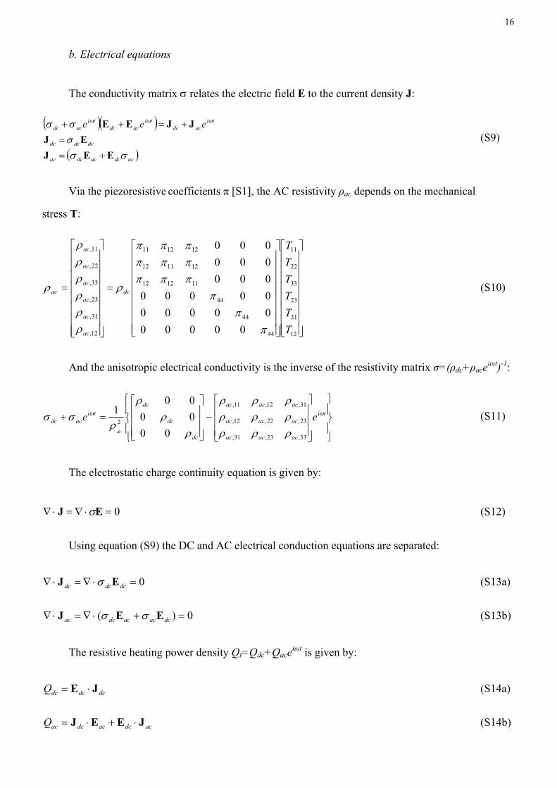
The conductivity matrix σ relates the electric field E to the current density J:
( )( )
( )acdcacdcac
dcdcdc
tiacdc
tiacdc
tiacdc eee
σσσσσ ωωω
EEJEJ
JJEE
+==
+=++ (S9)
Via the piezoresistive coefficients π [S1], the AC resistivity ρac depends on the mechanical
stress Τ:
⎥⎥⎥⎥⎥⎥⎥⎥
⎦
⎤
⎢⎢⎢⎢⎢⎢⎢⎢
⎣
⎡
⎥⎥⎥⎥⎥⎥⎥⎥
⎦
⎤
⎢⎢⎢⎢⎢⎢⎢⎢
⎣
⎡
=
⎥⎥⎥⎥⎥⎥⎥⎥
⎦
⎤
⎢⎢⎢⎢⎢⎢⎢⎢
⎣
⎡
=
12
31
23
33
22
11
44
44
44
111212
121112
121211
12,
31,
23,
33,
22,
11,
000000000000000000000000
TTTTTT
dc
ac
ac
ac
ac
ac
ac
ac
ππ
ππππππππππ
ρ
ρρρρρρ
ρ (S10)
And the anisotropic electrical conductivity is the inverse of the resistivity matrix σ=(ρdc+ρaceiωt)-1:
⎪⎭
⎪⎬
⎫
⎪⎩
⎪⎨
⎧
⎥⎥⎥
⎦
⎤
⎢⎢⎢
⎣
⎡−
⎥⎥⎥
⎦
⎤
⎢⎢⎢
⎣
⎡=+ ti
acacac
acacac
acacac
dc
dc
dcti
acdc eedc
ωω
ρρρρρρρρρ
ρρ
ρ
ρσσ
33,23,31,
23,22,12,
31,12,11,
2
000000
1 (S11)
The electrostatic charge continuity equation is given by:
0=⋅∇=⋅∇ EJ σ (S12)
Using equation (S9) the DC and AC electrical conduction equations are separated:
0=⋅∇=⋅∇ dcdcdc EJ σ (S13a)
0)( =+⋅∇=⋅∇ dcacacdcac EEJ σσ (S13b)
The resistive heating power density Qt=Qdc+Qaceiωt is given by:
dcdcdcQ JE ⋅= (S14a)
acdcacdcacQ JEEJ ⋅+⋅= (S14b)

17
c. Thermal equations
The equations governing the DC and AC thermal conduction are:
0)( =+∇⋅∇ dcdch QTk (S15a)
tiracpd
tirac
pdti
acti
rach eTciteT
ceQeTk ωω
ωω ωρρ ,,
, )( =∂
∂=+∇⋅∇ (S15b)
Here kh is the thermal conductivity, cp the specific heat capacity and ρd the mass density.
Convection is neglected since the device is operated in vacuum.
d. Mechanical equations
The mechanical partial differential equations consist of the equation of motion, the stress-strain
relation and the strain-displacement relation including thermal expansion:
racvecracs
racd
T
t
,,
2,
2
α
ρ
−∇==
∂∂
=⋅∇
uSScT
uT
(S16)
S is the strain vector field, T is the stress vector field and c is the stiffness tensor, ∇s is the
symmetric-gradient operator representing the strain-displacement relation, c is the cubic anisotropic
elasticity matrix of silicon and αvec is the thermal expansion vector for a cubic material:
⎥⎥⎥⎥⎥⎥⎥⎥
⎦
⎤
⎢⎢⎢⎢⎢⎢⎢⎢
⎣
⎡
=
⎥⎥⎥⎥⎥⎥⎥⎥
⎦
⎤
⎢⎢⎢⎢⎢⎢⎢⎢
⎣
⎡
=
000
000000000000000000000000
44
44
44
111212
121112
121211
t
t
t
vec
cc
cccccccccc
ααα
αc (S17)

18
e. Boundary conditions
The mechanical boundary conditions fix the structure (uac,r=0 m) at the anchors. The thermal
boundary conditions impose Tdc=0 K and Tac,r=0 K at the anchors and thermal insulation on all other
boundaries for both the AC and DC domain. The DC electrical boundary conditions impose Vdc=IdcRdc
at one anchor and Vdc=0 V at the other anchor. Because the device is connected to a current source the
AC electrical boundary conditions impose that the AC current density normal to the boundaries is zero
(n⋅Jac=0 A/m2).
f. FEM simulation
To solve the model, the partial differential equations discussed above have been incorporated in a
coupled model in Comsol Multiphysics 3.4 [S2]. The material parameters were taken from literature and
are shown in table S1. The geometry was taken from the mask design and the dimensions of the
nanobeam were measured more accurately using a scanning electron microscope. The measured
sacrificial layer underetch distance of 7 µm is included in the geometry of the anchors. To increase the
simulation speed and accuracy, the device was simulated in 2-dimensions by using the plane-strain
approximation. First the DC electrical equation (S13a) is solved. This gives Edc and Jdc which are
needed in equations (S13b) and (S14b). Then the coupled AC mechanical-thermal-electrical eigenvalue
equations (S13b),(S15b) and (S16) are solved, using the additional equations (S10), (S11), (S14b) and
(S17). This yields the eigenvectors of the lowest bending mode: uac,r(r), vac,r(r) and Tac,r(r). The solution
also gives the complex angular eigenfrequency ωres from which the effective Q-factor in the absence of
mechanical damping Qeff0 of the eigenmode can be calculated [S3] using the equation:
βωω Im
ReIm21 2
0dc
res
res
eff
IQ
−== (S18)
Because the device is an active component, the damping can be negative and therefore Qeff0 can be
negative. Since no mechanical damping was introduced, Qeff0 is purely a measure of the efficiency of the
feedback. Equation (S18) shows that Im β can be determined directly from the complex eigenfrequency
of the FEM simulation and the value of the DC current Idc. The DC thermal equation (S15a) can be
solved separately once the DC electrical equation (S13a) has been solved. The resulting DC thermal
distribution Tdc and the displacement mode-shape uac,r are shown in figure S2.

19
Supplementary Discussion 4: Extraction of equivalent parameters.
a. Equations to extract the parameters.
To quantitatively compare the value of Im β from the FEM model with the value from the
equivalent circuit shown in figure S1, the circuit parameter values are extracted from the FEM model.
This is done by choosing three reference positions rx, rT and rv in the FEM geometry and imposing the
condition that the variables in the equivalent circuit in figure S1 should equal the corresponding
variables in the FEM solution at these points: x(t)=uac,rx(rx)eiωt, Tac(t)=Tac,r(rT)eiωt and vac(t)=vac,r(rv)eiωt,
where uac,rx is the x-component of the displacement vector uac,r. The reference position rx is the centre-
of-mass of the rectangular mass, rT is the centre of the nanobeam and rv is the position of the anchor
boundary that is connected to the current source Idc. Using these variables, the piezoresistive constant
was determined from the FEM solution using:
xVvK
vdc
acpr )(r= (S19)
To determine the thermal parameters, first the total AC resistive heating power pac is determined
by integrating the AC heating power density Qac from equation (S14b) over the whole volume Volume of
the resonator:
∫=Volume
olumeacac dVQp (S20)
Although the integral is taken over the whole volume of the device, the AC resistive power Qac is
concentrated in the nanobeam as can be seen in figure S3. This AC heating power generates thermal
waves which are approximate solutions of the 1D heat equation cpρd∂ T/∂ t=kh∂ 2T/∂ y2. The 1D solution
T(y,t)= Tac,r(rT)e-2πy/λh ei(ωt-2πy/λh) consists of waves which emanate from the center of the nanobeam rT and
propagate along the y-axis with a thermal wavelength λh=(4πkh/[cpρdfres])1/2=26 µm and exponentially
decay in amplitude. The thermal wavelength and exponential decay correspond well to the thermal FEM
simulations of Tac,r in the oscillator as shown in figures S4 and S5.
To determine the effective thermal expansion coefficient α a separate mechanical FEM simulation
is performed, where the displacement xte as a result of the thermal expansion force of the AC

20
temperature distribution Tac,r is determined. From this simulation the effective thermal expansion
coefficient α is determined as:
acte Tx /=α (S21)
Using the values of pac, xte and α, the real thermal constants Rt and Ct can now be determined
from:
tt
acte RCi
px/1+
=ω
α (S22)
The values of the effective spring constant k and mass m are determined from fres=|ωres |/2π and the
integral over the strain energy using the method described in reference [S3].
b. Experimental determination of Kpr
Before determining the parameter values from the FEM simulation using the equations (S19-S22),
the effective piezoresistive gauge factor Kpr=rac/(Rdcx) is approximated [S4] from the transconductance
gm curves in figure 2a. The displacement amplitude at resonance when the device is externally excited
by an electrostatic force Fel.st. is approximately given by |xpeak|=Qint|Fel.st|/k. The effective spring constant
k was estimated with a finite element method to be k=256 N/m. For small displacements, the AC
electrostatic force in the parallel plate approximation is given by Fel.st.=(ε0vact,acVact,dcΑact)/gact2. The area
and gap of the actuation electrode are respectively Aact=60.0×1.5 µm2 and gact=200 nm, and ε0 is the
vacuum permittivity. When the output is AC-grounded, the AC piezoresistive current is given by
iac,pr=-Idcrac/Rdc and the transconductance is defined as gm=iac,pr/vact,ac. From the fits in figure 2a, the peak
transconductance gm,peak and the intrinsic Q-factor Qint were determined. It is found that
|gm,peak|/Qint=5.0×10-9 S, for Idc=0.1 mA and Vact,dc=-1.0 V. In combination with the equations and
constants above, this allows the effective piezoresistive gauge factor to be estimated:
Kpr=(gm,peak/Qint)×(kgact2/(ε0IdcVact,dcΑact))=-6.4×105 m-1, where the negative sign of Kpr was determined
using the phase of gm,peak.

21
c. Parameter values
The simulated parameter values as obtained from the FEM simulations using equations (S18-S22)
are summarized in table S2 next to the measured values. The simulated resonance frequency fres is
slightly higher than the measured value. This can partly be attributed to the use of the 2D plane-strain
approximation. A simulation in the plane-stress approximation resulted in fres=1.278 MHz, closer to the
measured value. The simulated DC resistance is found from Rdc=Vdc(rv)/Idc. It is lower than the
measured value because not the full electrical geometry was simulated. A consequence of this is that the
value of Kpr is different because it depends on Rdc, via Kprx=rac/Rdc. It is therefore better to compare the
product KprRdc. If the simulated parameters from table S2 are substituted into equation (S1) a value of
Im β=αRdcKprIm(1/[(1/Rt+iωresCt)])=58 A-2 is found, which is identical to the complex eigenvalue
obtained using equation (S18) thus supporting the validity of equation (S1).

22
II. Supplementary Figures
Figure S1 Equivalent small-signal circuit model of the oscillator. In this supplementary
information, this model is discussed in more detail. Moreover, finite element simulations are
presented to verify the model and to extract the model parameters. This figure is identical to
figure 3b in the main paper.

23
Figure S2 Mechanical bending mode-shape uac,r at maximal displacement (x=-2 µm) and the
current induced DC temperature change Tdc (K) of the oscillator, which is indicated by the
color-scale for Idc=1.2 mA. Because the actual amplitude of the oscillator is estimated to be
only 43 nm (see legend of figure 2), the mechanical amplitude and the corresponding AC
heating power and AC temperature in figures S3 and S4 are exaggerated by a factor 47.

24
Figure S3 AC resistive heating power density Qac (W/m3) for x=-2 µm and Idc=1.2 mA.
Essentially all AC power is generated in the nanobeam.

25
Figure S4 The AC temperature |Tac,r|(K) for an amplitude x0=2 µm and Idc=1.2 mA. The
temperature decreases exponentially with distance from the nanobeam.

26
Figure S5 Phase of the thermal waves plotted as sin(arctan(Im(Tac,r)/Re(Tac,r))). The
wavelength of the thermal waves is close to λh=26 µm as predicted by the 1D heat equation
(see Supplementary Discussion 4a).

27
III. Supplementary Tables
Table S1 FEM material parameters at room temperature.
Parameter Value Reference
c11 (GPa) 166 [S5]
c12 (GPa) 64 [S5]
c44 (GPa) 80 [S5]
ρd (kg/m3) 2329
ρdc(Ω⋅m) 10-4
αt (K-1) 2.6×10⁻⁶ [S7]
π11 (Pa-1) -102.2×10⁻¹¹ [S1]
π12 (Pa-1) 53.4×10⁻¹¹ [S1]
π44 (Pa-1) -13.6×10⁻¹¹ [S1]
cp (J/(kg⋅K)) 702
kh (W/(m⋅K)) 113 [S6]

28
Table S2 Oscillator parameters.
FEM Simulation Measured
fres (MHz) 1.335 1.258
Im β (A-2) 58 50
Rdc (Ω) 583 824
Kpr (m-1) -8.35×10⁵ -6.4×10⁵
KprRdc (MΩ/m) -487 -527
α (m/K) 43.1×10⁻¹²
Rt (K/W) 6.74×10³
Ct (J/K) 9.29×10⁻¹²
k (N/m) 256
M (kg) 3.64×10⁻¹²

29
IV. Supplementary References
[S1] Smith, C. S., Piezoresistance effect in germanium and silicon. Phys. Rev., 94, 42-49, (1954).
[S2] Comsol Multiphysics, http://www.comsol.com.
[S3] Steeneken, P.G. et al., Parameter extraction and support-loss in MEMS resonators. Proc. Comsol
conf., 725-730 (2007).
[S4] van Beek, J.T.M., Steeneken, P.G. and Giesbers, B., A 10 MHz Piezoresistive MEMS resonator
with high-Q. Proc. Int. Freq. Contr. Symp., 475-480 (2006).
[S5] Wortman, J.J. and Evans, R. A., Young’s modulus, shear modulus, and Poisson’s ratio in silicon
and germanium, J. Appl. Phys., 36, 153–156, (1965).
[S6] Asheghi, M., Kurabayashi, K., Kasnavi, R., and Goodson, K. E., Thermal conduction in doped
single-crystal silicon films. J. Appl. Phys., 91, 5079–5088, (2002).
[S7] Okada, Y. and Tokumaru, Y., Precise determination of lattice parameter and thermal expansion
coefficient of silicon between 300 and 1500 K. J. Appl. Phys., 56, 314, (1984).