Embed Size (px)
Citation preview
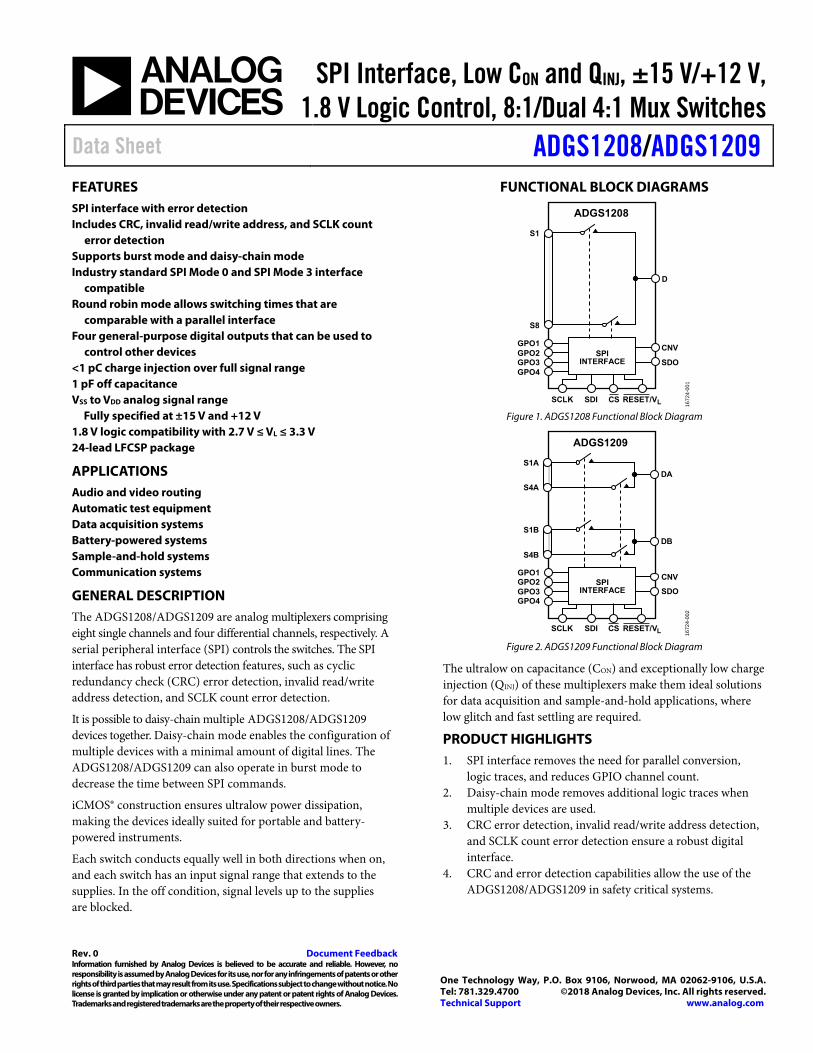
SPI Interface, Low CON and QINJ, ±15 V/+12 V, 1.8 V Logic Control, 8:1/Dual 4:1 Mux Switches
Data Sheet ADGS1208/ADGS1209
Rev. 0 Document Feedback Information furnished by Analog Devices is believed to be accurate and reliable. However, no responsibility is assumed by Analog Devices for its use, nor for any infringements of patents or other rights of third parties that may result from its use. Specifications subject to change without notice. No license is granted by implication or otherwise under any patent or patent rights of Analog Devices. Trademarks and registered trademarks are the property of their respective owners.
One Technology Way, P.O. Box 9106, Norwood, MA 02062-9106, U.S.A.Tel: 781.329.4700 ©2018 Analog Devices, Inc. All rights reserved. Technical Support www.analog.com
FEATURES SPI interface with error detection Includes CRC, invalid read/write address, and SCLK count
error detection Supports burst mode and daisy-chain mode Industry standard SPI Mode 0 and SPI Mode 3 interface
compatible Round robin mode allows switching times that are
comparable with a parallel interface Four general-purpose digital outputs that can be used to
control other devices <1 pC charge injection over full signal range 1 pF off capacitance VSS to VDD analog signal range
Fully specified at ±15 V and +12 V 1.8 V logic compatibility with 2.7 V ≤ VL ≤ 3.3 V 24-lead LFCSP package
APPLICATIONS Audio and video routing Automatic test equipment Data acquisition systems Battery-powered systems Sample-and-hold systems Communication systems
GENERAL DESCRIPTION The ADGS1208/ADGS1209 are analog multiplexers comprising eight single channels and four differential channels, respectively. A serial peripheral interface (SPI) controls the switches. The SPI interface has robust error detection features, such as cyclic redundancy check (CRC) error detection, invalid read/write address detection, and SCLK count error detection.
It is possible to daisy-chain multiple ADGS1208/ADGS1209 devices together. Daisy-chain mode enables the configuration of multiple devices with a minimal amount of digital lines. The ADGS1208/ADGS1209 can also operate in burst mode to decrease the time between SPI commands.
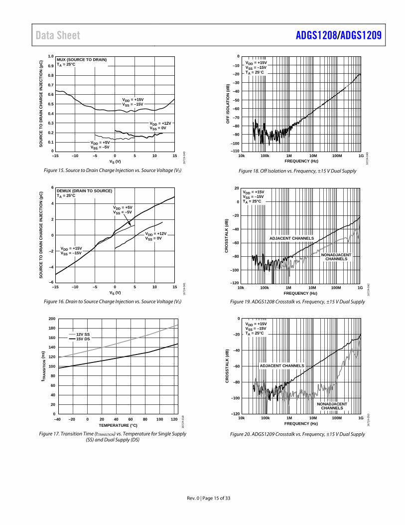
iCMOS® construction ensures ultralow power dissipation, making the devices ideally suited for portable and battery-powered instruments.
Each switch conducts equally well in both directions when on, and each switch has an input signal range that extends to the supplies. In the off condition, signal levels up to the supplies are blocked.
FUNCTIONAL BLOCK DIAGRAMS
ADGS1208
S1
S8
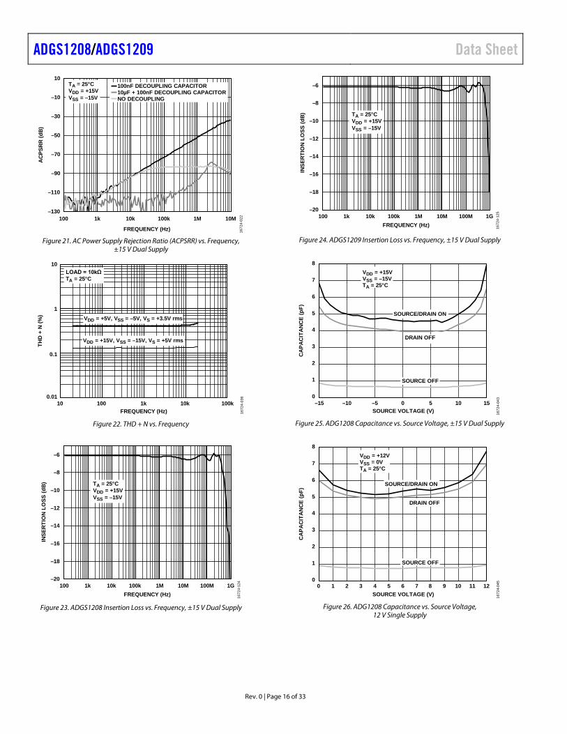
GPO1 CNV
SDOGPO2GPO3GPO4
D
SPIINTERFACE
SCLK SDI CS RESET/VL 1672
4-00
1
Figure 1. ADGS1208 Functional Block Diagram
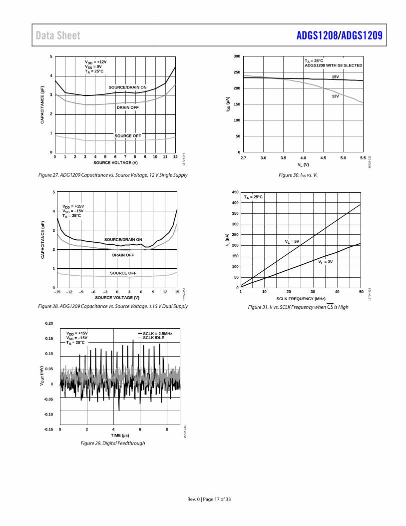
GPO1 CNV
SDOGPO2GPO3GPO4
SPIINTERFACE
SCLK SDI CS RESET/VL 1672
4-00
2
ADGS1209
S1A
S4B
DA
DB
S4A
S1B
Figure 2. ADGS1209 Functional Block Diagram
The ultralow on capacitance (CON) and exceptionally low charge injection (QINJ) of these multiplexers make them ideal solutions for data acquisition and sample-and-hold applications, where low glitch and fast settling are required.
PRODUCT HIGHLIGHTS 1. SPI interface removes the need for parallel conversion,
logic traces, and reduces GPIO channel count. 2. Daisy-chain mode removes additional logic traces when
multiple devices are used. 3. CRC error detection, invalid read/write address detection,
and SCLK count error detection ensure a robust digital interface.
4. CRC and error detection capabilities allow the use of the ADGS1208/ADGS1209 in safety critical systems.
ADGS1208/ADGS1209 Data Sheet
Rev. 0 | Page 2 of 33
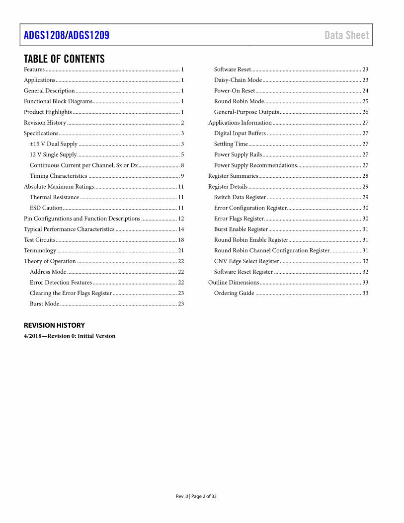
TABLE OF CONTENTS Features .............................................................................................. 1 Applications ....................................................................................... 1 General Description ......................................................................... 1 Functional Block Diagrams ............................................................. 1 Product Highlights ........................................................................... 1 Revision History ............................................................................... 2 Specifications ..................................................................................... 3
±15 V Dual Supply ....................................................................... 3 12 V Single Supply ........................................................................ 5 Continuous Current per Channel, Sx or Dx ............................. 8 Timing Characteristics ................................................................ 9
Absolute Maximum Ratings .......................................................... 11 Thermal Resistance .................................................................... 11 ESD Caution ................................................................................ 11
Pin Configurations and Function Descriptions ......................... 12 Typical Performance Characteristics ........................................... 14 Test Circuits ..................................................................................... 18 Terminology .................................................................................... 21 Theory of Operation ...................................................................... 22
Address Mode ............................................................................. 22 Error Detection Features ........................................................... 22 Clearing the Error Flags Register ............................................. 23 Burst Mode .................................................................................. 23
Software Reset ............................................................................. 23 Daisy-Chain Mode ..................................................................... 23 Power-On Reset .......................................................................... 24 Round Robin Mode.................................................................... 25 General-Purpose Outputs ......................................................... 26
Applications Information .............................................................. 27 Digital Input Buffers .................................................................. 27 Settling Time ............................................................................... 27 Power Supply Rails ..................................................................... 27 Power Supply Recommendations ............................................. 27
Register Summaries ........................................................................ 28 Register Details ............................................................................... 29
Switch Data Register .................................................................. 29 Error Configuration Register .................................................... 30 Error Flags Register .................................................................... 30 Burst Enable Register ................................................................. 31 Round Robin Enable Register ................................................... 31 Round Robin Channel Configuration Register...................... 31 CNV Edge Select Register ......................................................... 32 Software Reset Register ............................................................. 32
Outline Dimensions ....................................................................... 33 Ordering Guide .......................................................................... 33
REVISION HISTORY 4/2018—Revision 0: Initial Version
Data Sheet ADGS1208/ADGS1209
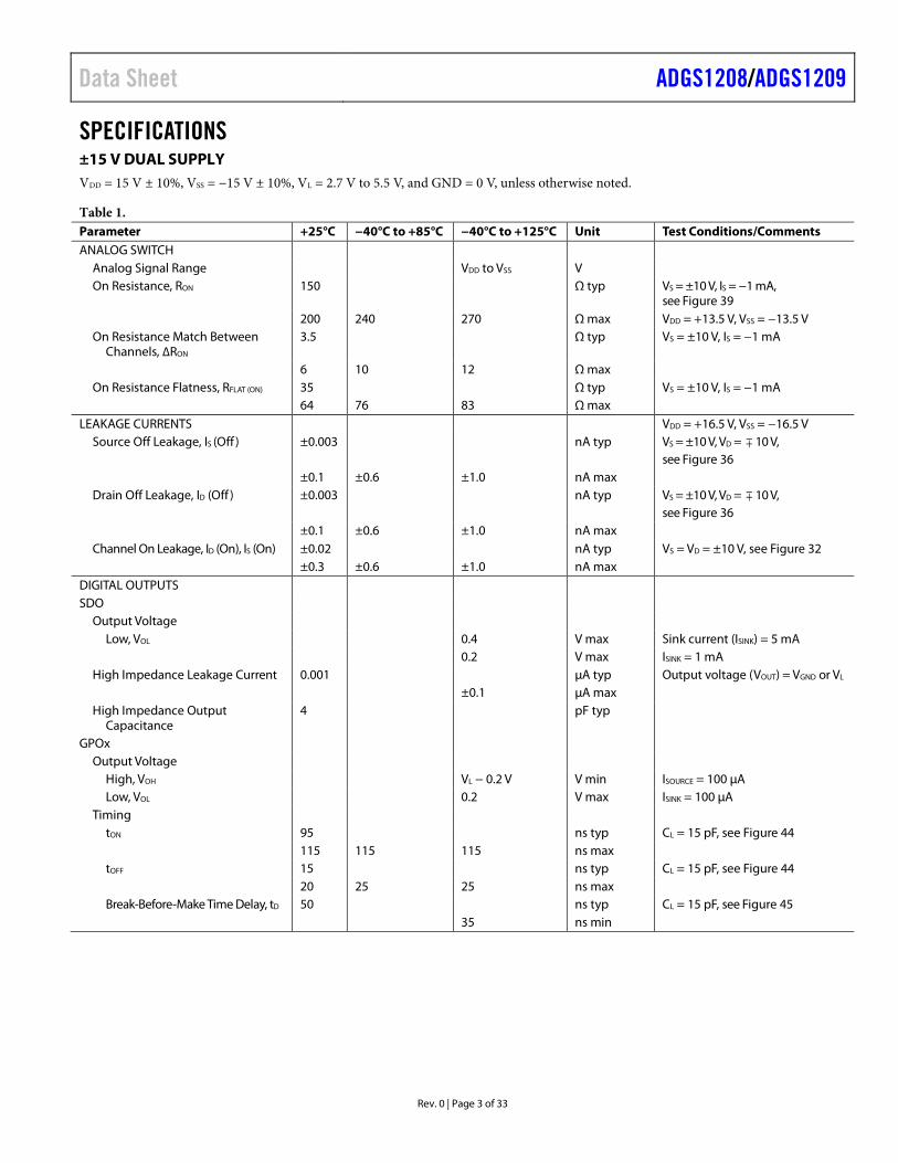
Rev. 0 | Page 3 of 33
SPECIFICATIONS ±15 V DUAL SUPPLY VDD = 15 V ± 10%, VSS = −15 V ± 10%, VL = 2.7 V to 5.5 V, and GND = 0 V, unless otherwise noted.
Table 1. Parameter +25°C −40°C to +85°C −40°C to +125°C Unit Test Conditions/Comments ANALOG SWITCH
Analog Signal Range VDD to VSS V On Resistance, RON 150 Ω typ VS = ±10 V, IS = −1 mA,
see Figure 39 200 240 270 Ω max VDD = +13.5 V, VSS = −13.5 V On Resistance Match Between
Channels, ∆RON 3.5 Ω typ VS = ±10 V, IS = −1 mA
6 10 12 Ω max On Resistance Flatness, RFLAT (ON) 35 Ω typ VS = ±10 V, IS = −1 mA
64 76 83 Ω max LEAKAGE CURRENTS VDD = +16.5 V, VSS = −16.5 V
Source Off Leakage, IS (Off ) ±0.003 nA typ VS = ±10 V, VD = 10 V, see Figure 36
±0.1 ±0.6 ±1.0 nA max Drain Off Leakage, ID (Off ) ±0.003 nA typ VS = ±10 V, VD = 10 V,
see Figure 36 ±0.1 ±0.6 ±1.0 nA max Channel On Leakage, ID (On), IS (On) ±0.02 nA typ VS = VD = ±10 V, see Figure 32
±0.3 ±0.6 ±1.0 nA max DIGITAL OUTPUTS SDO
Output Voltage Low, VOL 0.4 V max Sink current (ISINK) = 5 mA 0.2 V max ISINK = 1 mA
High Impedance Leakage Current 0.001 µA typ Output voltage (VOUT) = VGND or VL ±0.1 µA max High Impedance Output
Capacitance 4 pF typ
GPOx Output Voltage
High, VOH VL − 0.2 V V min ISOURCE = 100 µA Low, VOL 0.2 V max ISINK = 100 µA
Timing tON 95 ns typ CL = 15 pF, see Figure 44 115 115 115 ns max tOFF 15 ns typ CL = 15 pF, see Figure 44 20 25 25 ns max Break-Before-Make Time Delay, tD 50 ns typ CL = 15 pF, see Figure 45
35 ns min
ADGS1208/ADGS1209 Data Sheet
Rev. 0 | Page 4 of 33
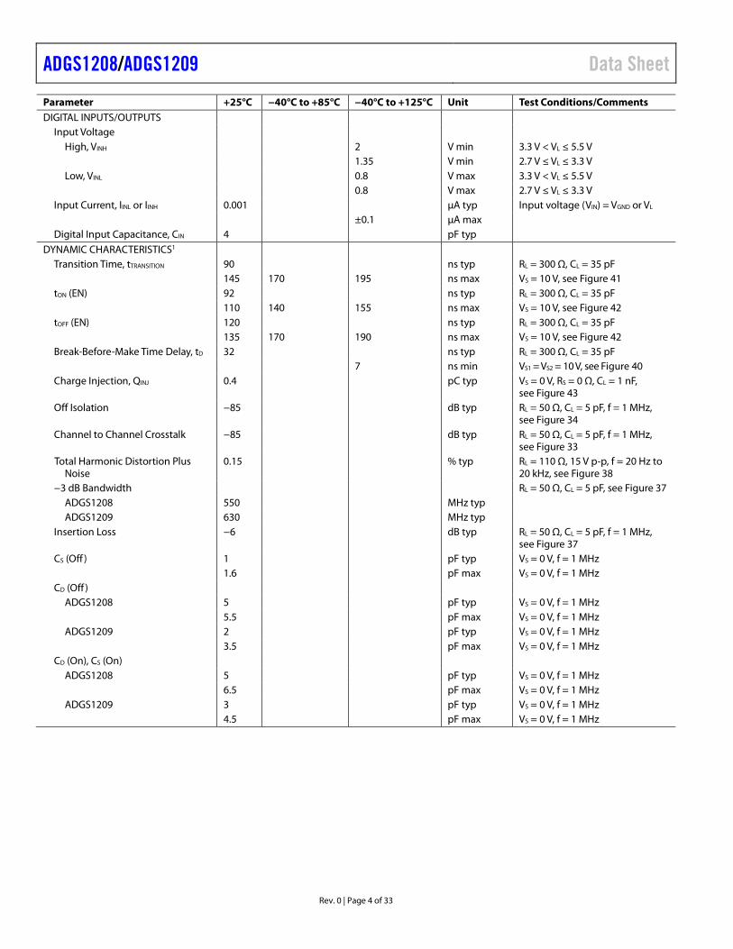
Parameter +25°C −40°C to +85°C −40°C to +125°C Unit Test Conditions/Comments DIGITAL INPUTS/OUTPUTS
Input Voltage High, VINH 2 V min 3.3 V < VL ≤ 5.5 V 1.35 V min 2.7 V ≤ VL ≤ 3.3 V Low, VINL 0.8 V max 3.3 V < VL ≤ 5.5 V 0.8 V max 2.7 V ≤ VL ≤ 3.3 V
Input Current, IINL or IINH 0.001 µA typ Input voltage (VIN) = VGND or VL ±0.1 µA max Digital Input Capacitance, CIN 4 pF typ
DYNAMIC CHARACTERISTICS1 Transition Time, tTRANSITION 90 ns typ RL = 300 Ω, CL = 35 pF 145 170 195 ns max VS = 10 V, see Figure 41 tON (EN) 92 ns typ RL = 300 Ω, CL = 35 pF 110 140 155 ns max VS = 10 V, see Figure 42 tOFF (EN) 120 ns typ RL = 300 Ω, CL = 35 pF 135 170 190 ns max VS = 10 V, see Figure 42 Break-Before-Make Time Delay, tD 32 ns typ RL = 300 Ω, CL = 35 pF 7 ns min VS1 = VS2 = 10 V, see Figure 40 Charge Injection, QINJ 0.4 pC typ VS = 0 V, RS = 0 Ω, CL = 1 nF,
see Figure 43 Off Isolation −85 dB typ RL = 50 Ω, CL = 5 pF, f = 1 MHz,
see Figure 34 Channel to Channel Crosstalk −85 dB typ RL = 50 Ω, CL = 5 pF, f = 1 MHz,
see Figure 33 Total Harmonic Distortion Plus
Noise 0.15 % typ RL = 110 Ω, 15 V p-p, f = 20 Hz to
20 kHz, see Figure 38 −3 dB Bandwidth RL = 50 Ω, CL = 5 pF, see Figure 37
ADGS1208 550 MHz typ ADGS1209 630 MHz typ
Insertion Loss −6 dB typ RL = 50 Ω, CL = 5 pF, f = 1 MHz, see Figure 37
CS (Off ) 1 pF typ VS = 0 V, f = 1 MHz 1.6 pF max VS = 0 V, f = 1 MHz CD (Off )
ADGS1208 5 pF typ VS = 0 V, f = 1 MHz 5.5 pF max VS = 0 V, f = 1 MHz ADGS1209 2 pF typ VS = 0 V, f = 1 MHz 3.5 pF max VS = 0 V, f = 1 MHz
CD (On), CS (On) ADGS1208 5 pF typ VS = 0 V, f = 1 MHz 6.5 pF max VS = 0 V, f = 1 MHz ADGS1209 3 pF typ VS = 0 V, f = 1 MHz 4.5 pF max VS = 0 V, f = 1 MHz
Data Sheet ADGS1208/ADGS1209
Rev. 0 | Page 5 of 33
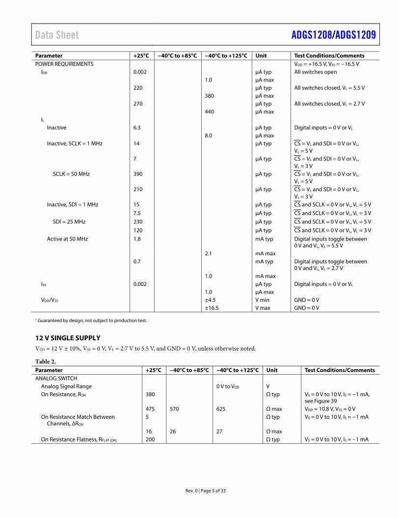
Parameter +25°C −40°C to +85°C −40°C to +125°C Unit Test Conditions/Comments POWER REQUIREMENTS VDD = +16.5 V, VSS = −16.5 V
IDD 0.002 μA typ All switches open 1.0 μA max 220 μA typ All switches closed, VL = 5.5 V 380 μA max 270 μA typ All switches closed, VL = 2.7 V 440 μA max IL
Inactive 6.3 μA typ Digital inputs = 0 V or VL 8.0 μA max Inactive, SCLK = 1 MHz 14 μA typ CS E = VL and SDI = 0 V or VL,
VL = 5 V 7 μA typ CS E = VL and SDI = 0 V or VL,
VL = 3 V SCLK = 50 MHz 390 μA typ CS E = VL and SDI = 0 V or VL,
VL = 5 V 210 μA typ CS E = VL and SDI = 0 V or VL,
VL = 3 V Inactive, SDI = 1 MHz 15 μA typ CS E and SCLK = 0 V or VL, VL = 5 V
7.5 μA typ CS E and SCLK = 0 V or VL, VL = 3 V
SDI = 25 MHz 230 μA typ CS E and SCLK = 0 V or VL, VL = 5 V
120 μA typ CS E and SCLK = 0 V or VL, VL = 3 V
Active at 50 MHz 1.8 mA typ Digital inputs toggle between 0 V and VL, VL = 5.5 V
2.1 mA max 0.7 mA typ Digital inputs toggle between
0 V and VL, VL = 2.7 V 1.0 mA max
ISS 0.002 μA typ Digital inputs = 0 V or VL 1.0 μA max VDD/VSS ±4.5 V min GND = 0 V ±16.5 V max GND = 0 V
1 Guaranteed by design; not subject to production test.
12 V SINGLE SUPPLY VDD = 12 V ± 10%, VSS = 0 V, VL = 2.7 V to 5.5 V, and GND = 0 V, unless otherwise noted.
Table 2. Parameter +25°C −40°C to +85°C −40°C to +125°C Unit Test Conditions/Comments ANALOG SWITCH
Analog Signal Range 0 V to VDD V On Resistance, RON 380 Ω typ VS = 0 V to 10 V, IS = −1 mA,
see Figure 39 475 570 625 Ω max VDD = 10.8 V, VSS = 0 V On Resistance Match Between
Channels, ∆RON 5 Ω typ VS = 0 V to 10 V, IS = −1 mA
16 26 27 Ω max On Resistance Flatness, RFLAT (ON) 200 Ω typ VS = 0 V to 10 V, IS = −1 mA
ADGS1208/ADGS1209 Data Sheet
Rev. 0 | Page 6 of 33
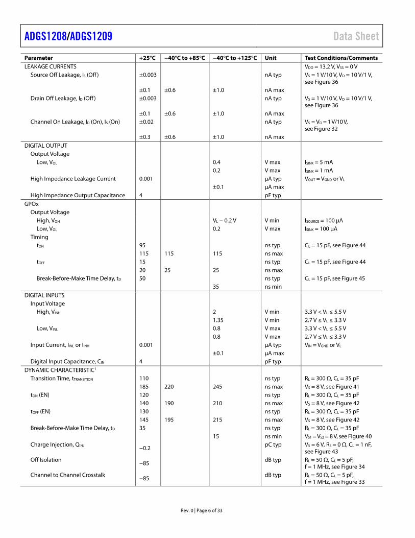
Parameter +25°C −40°C to +85°C −40°C to +125°C Unit Test Conditions/Comments LEAKAGE CURRENTS VDD = 13.2 V, VSS = 0 V
Source Off Leakage, IS (Off ) ±0.003 nA typ VS = 1 V/10 V, VD = 10 V/1 V, see Figure 36
±0.1 ±0.6 ±1.0 nA max Drain Off Leakage, ID (Off ) ±0.003 nA typ VS = 1 V/10 V, VD = 10 V/1 V,
see Figure 36 ±0.1 ±0.6 ±1.0 nA max Channel On Leakage, ID (On), IS (On) ±0.02 nA typ VS = VD = 1 V/10 V,
see Figure 32 ±0.3 ±0.6 ±1.0 nA max DIGITAL OUTPUT
Output Voltage Low, VOL 0.4 V max ISINK = 5 mA 0.2 V max ISINK = 1 mA
High Impedance Leakage Current 0.001 µA typ VOUT = VGND or VL ±0.1 µA max High Impedance Output Capacitance 4 pF typ
GPOx Output Voltage
High, VOH VL − 0.2 V V min ISOURCE = 100 µA Low, VOL 0.2 V max ISINK = 100 µA
Timing tON 95 ns typ CL = 15 pF, see Figure 44 115 115 115 ns max tOFF 15 ns typ CL = 15 pF, see Figure 44 20 25 25 ns max Break-Before-Make Time Delay, tD 50 ns typ CL = 15 pF, see Figure 45
35 ns min DIGITAL INPUTS
Input Voltage High, VINH 2 V min 3.3 V < VL ≤ 5.5 V 1.35 V min 2.7 V ≤ VL ≤ 3.3 V Low, VINL 0.8 V max 3.3 V < VL ≤ 5.5 V 0.8 V max 2.7 V ≤ VL ≤ 3.3 V
Input Current, IINL or IINH 0.001 µA typ VIN = VGND or VL ±0.1 µA max Digital Input Capacitance, CIN 4 pF typ
DYNAMIC CHARACTERISTIC1 Transition Time, tTRANSITION 110 ns typ RL = 300 Ω, CL = 35 pF 185 220 245 ns max VS = 8 V, see Figure 41 tON (EN) 120 ns typ RL = 300 Ω, CL = 35 pF 140 190 210 ns max VS = 8 V, see Figure 42 tOFF (EN) 130 ns typ RL = 300 Ω, CL = 35 pF 145 195 215 ns max VS = 8 V, see Figure 42 Break-Before-Make Time Delay, tD 35 ns typ RL = 300 Ω, CL = 35 pF 15 ns min VS1 = VS2 = 8 V, see Figure 40 Charge Injection, QINJ −0.2
pC typ VS = 6 V, RS = 0 Ω, CL = 1 nF, see Figure 43
Off Isolation −85 dB typ RL = 50 Ω, CL = 5 pF, f = 1 MHz, see Figure 34
Channel to Channel Crosstalk −85 dB typ RL = 50 Ω, CL = 5 pF, f = 1 MHz, see Figure 33
Data Sheet ADGS1208/ADGS1209
Rev. 0 | Page 7 of 33
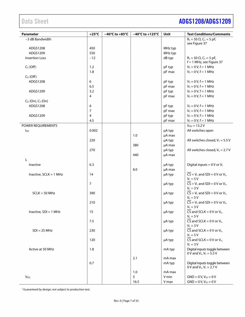
Parameter +25°C −40°C to +85°C −40°C to +125°C Unit Test Conditions/Comments −3 dB Bandwidth RL = 50 Ω, CL = 5 pF,
see Figure 37 ADGS1208 450 MHz typ ADGS1209 550 MHz typ
Insertion Loss −12 dB typ RL = 50 Ω, CL = 5 pF, f = 1 MHz, see Figure 37
CS (Off ) 1.2 pF typ VS = 0 V, f = 1 MHz 1.8 pF max VS = 0 V, f = 1 MHz CD (Off )
ADGS1208 6 pF typ VS = 0 V, f = 1 MHz 6.5 pF max VS = 0 V, f = 1 MHz ADGS1209 3.2 pF typ VS = 0 V, f = 1 MHz 4 pF max VS = 0 V, f = 1 MHz
CD (On), CS (On) ADGS1208 6 pF typ VS = 0 V, f = 1 MHz 7 pF max VS = 0 V, f = 1 MHz ADGS1209 4 pF typ VS = 0 V, f = 1 MHz 4.5 pF max VS = 0 V, f = 1 MHz
POWER REQUIREMENTS VDD = 13.2 V IDD 0.002 µA typ All switches open 1.0 µA max 220 µA typ All switches closed, VL = 5.5 V 380 µA max 270 µA typ All switches closed, VL = 2.7 V 440 µA max IL
Inactive 6.3 µA typ Digital inputs = 0 V or VL 8.0 µA max Inactive, SCLK = 1 MHz 14 µA typ CS = VL and SDI = 0 V or VL,
VL = 5 V 7 µA typ CS = VL and SDI = 0 V or VL,
VL = 3 V SCLK = 50 MHz 390 µA typ CS = VL and SDI = 0 V or VL,
VL = 5 V 210 µA typ CS = VL and SDI = 0 V or VL,
VL = 3 V Inactive, SDI = 1 MHz 15 µA typ CS and SCLK = 0 V or VL,
VL = 5 V 7.5 µA typ CS and SCLK = 0 V or VL,
VL = 3 V SDI = 25 MHz 230 µA typ CS and SCLK = 0 V or VL,
VL = 5 V 120 µA typ CS and SCLK = 0 V or VL,
VL = 3 V Active at 50 MHz 1.8 mA typ Digital inputs toggle between
0 V and VL, VL = 5.5 V 2.1 mA max 0.7 mA typ Digital inputs toggle between
0 V and VL, VL = 2.7 V 1.0 mA max
VDD 5 V min GND = 0 V, VSS = 0 V 16.5 V max GND = 0 V, VSS = 0 V
1 Guaranteed by design; not subject to production test.
ADGS1208/ADGS1209 Data Sheet
Rev. 0 | Page 8 of 33
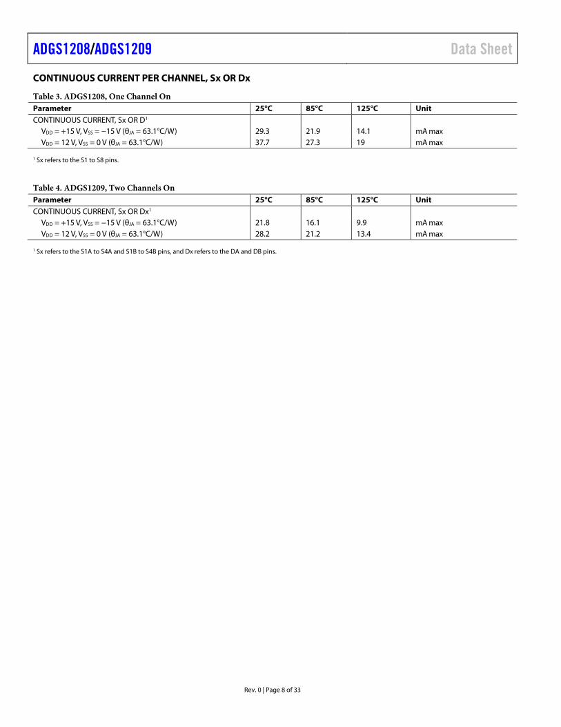
CONTINUOUS CURRENT PER CHANNEL, Sx OR Dx
Table 3. ADGS1208, One Channel On Parameter 25°C 85°C 125°C Unit CONTINUOUS CURRENT, Sx OR D1
VDD = +15 V, VSS = −15 V (θJA = 63.1°C/W) 29.3 21.9 14.1 mA max VDD = 12 V, VSS = 0 V (θJA = 63.1°C/W) 37.7 27.3 19 mA max
1 Sx refers to the S1 to S8 pins.
Table 4. ADGS1209, Two Channels On Parameter 25°C 85°C 125°C Unit CONTINUOUS CURRENT, Sx OR Dx1
VDD = +15 V, VSS = −15 V (θJA = 63.1°C/W) 21.8 16.1 9.9 mA max VDD = 12 V, VSS = 0 V (θJA = 63.1°C/W) 28.2 21.2 13.4 mA max
1 Sx refers to the S1A to S4A and S1B to S4B pins, and Dx refers to the DA and DB pins.
Data Sheet ADGS1208/ADGS1209
Rev. 0 | Page 9 of 33
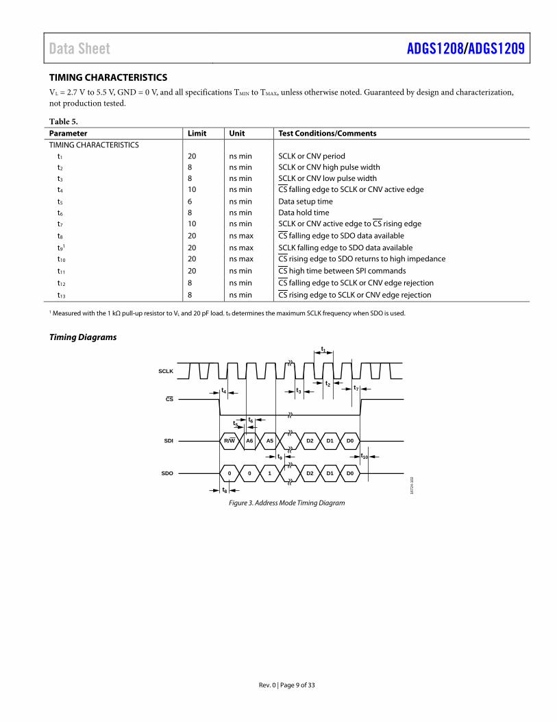
TIMING CHARACTERISTICS VL = 2.7 V to 5.5 V, GND = 0 V, and all specifications TMIN to TMAX, unless otherwise noted. Guaranteed by design and characterization, not production tested.
Table 5. Parameter Limit Unit Test Conditions/Comments TIMING CHARACTERISTICS
t1 20 ns min SCLK or CNV period t2 8 ns min SCLK or CNV high pulse width t3 8 ns min SCLK or CNV low pulse width t4 10 ns min CS falling edge to SCLK or CNV active edge
t5 6 ns min Data setup time t6 8 ns min Data hold time t7 10 ns min SCLK or CNV active edge to CS rising edge
t8 20 ns max CS falling edge to SDO data available
t91 20 ns max SCLK falling edge to SDO data available
t10 20 ns max CS rising edge to SDO returns to high impedance
t11 20 ns min CS high time between SPI commands
t12 8 ns min CS falling edge to SCLK or CNV edge rejection
t13 8 ns min CS rising edge to SCLK or CNV edge rejection 1 Measured with the 1 kΩ pull-up resistor to VL and 20 pF load. t9 determines the maximum SCLK frequency when SDO is used.
Timing Diagrams t1
t2t3t4
t5
t8
t9 t10
t6
t7
R/W
CS
SCLK
SDI
SDO
A6 A5 D2 D1 D0
0 0 1 D2 D1 D0
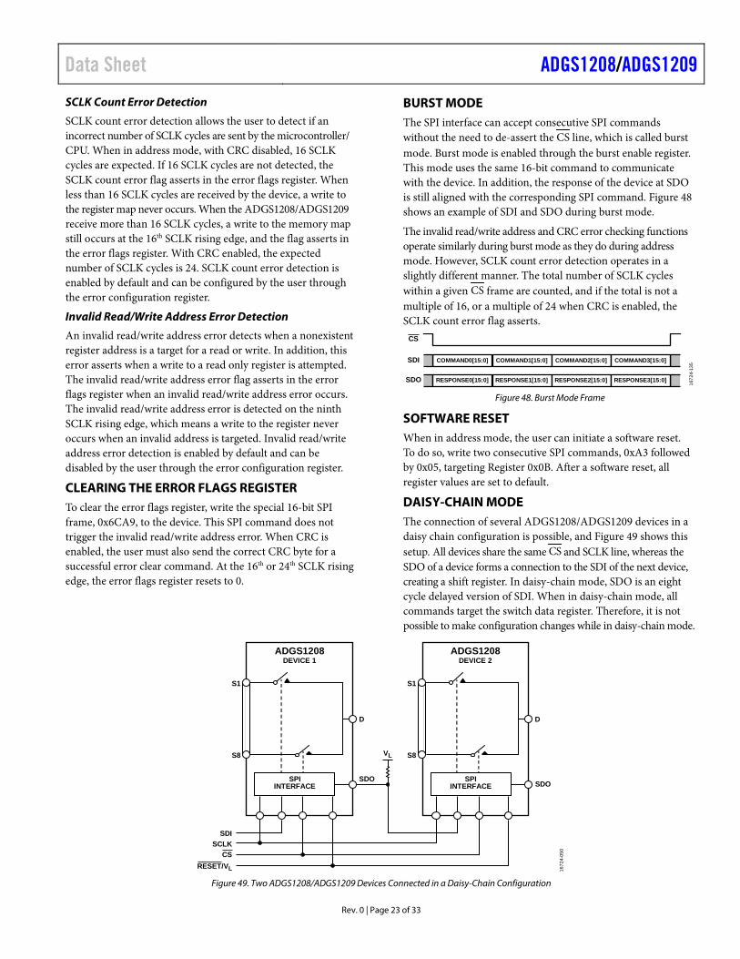
1672
4-10
2
Figure 3. Address Mode Timing Diagram
ADGS1208/ADGS1209 Data Sheet
Rev. 0 | Page 10 of 33
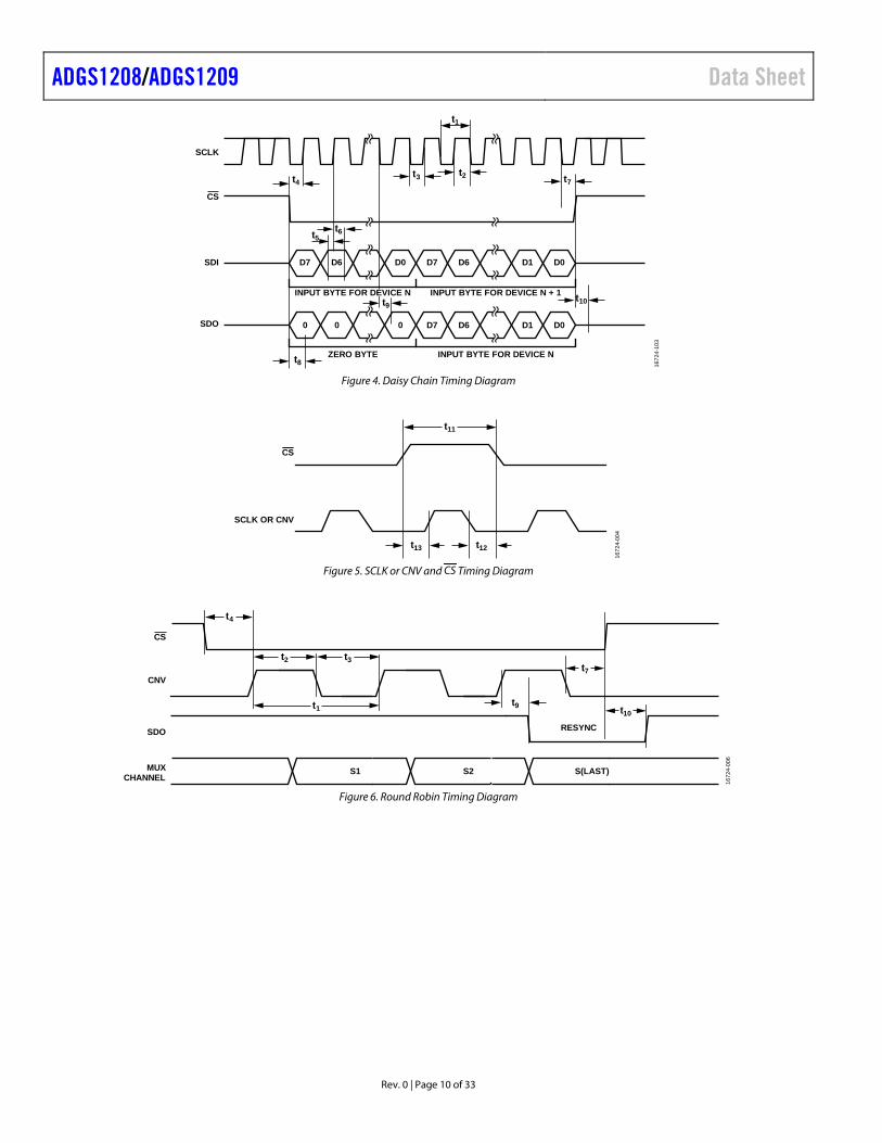
t1
t2t3t4
t5
t8
t9t10
t6
t7
CS
SCLK
SDI
SDO
INPUT BYTE FOR DEVICE N + 1
ZERO BYTE INPUT BYTE FOR DEVICE N
D7 D6 D0 D7 D6 D1 D0
0 0 0 D7 D6 D1 D0
1672
4-10
3
INPUT BYTE FOR DEVICE N
Figure 4. Daisy Chain Timing Diagram
SCLK OR CNV
CS
t11
t12t13
1672
4-00
4
Figure 5. SCLK or CNV and CS Timing Diagram
CNV
MUXCHANNEL
S1 S2 S(LAST)
SDO RESYNC
CS
t3t2
t1
t4
t9
t7
t10
1672
4-00
6
Figure 6. Round Robin Timing Diagram
Data Sheet ADGS1208/ADGS1209
Rev. 0 | Page 11 of 33
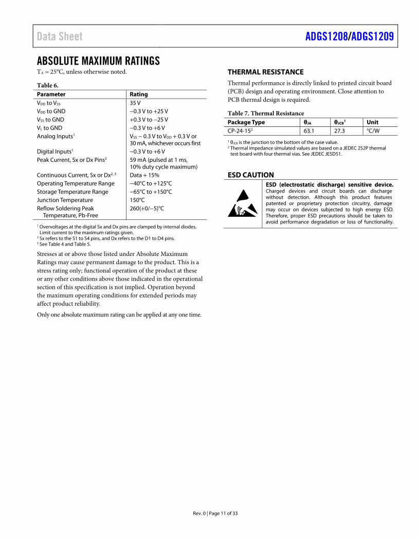
ABSOLUTE MAXIMUM RATINGS TA = 25°C, unless otherwise noted.
Table 6. Parameter Rating VDD to VSS 35 V VDD to GND −0.3 V to +25 V VSS to GND +0.3 V to −25 V VL to GND −0.3 V to +6 V Analog Inputs1 VSS − 0.3 V to VDD + 0.3 V or
30 mA, whichever occurs first Digital Inputs1 −0.3 V to +6 V Peak Current, Sx or Dx Pins2 59 mA (pulsed at 1 ms,
10% duty cycle maximum) Continuous Current, Sx or Dx2, 3 Data + 15% Operating Temperature Range −40°C to +125°C Storage Temperature Range −65°C to +150°C Junction Temperature 150°C Reflow Soldering Peak
Temperature, Pb-Free 260(+0/−5)°C
1 Overvoltages at the digital Sx and Dx pins are clamped by internal diodes. Limit current to the maximum ratings given.
2 Sx refers to the S1 to S4 pins, and Dx refers to the D1 to D4 pins. 3 See Table 4 and Table 5.
Stresses at or above those listed under Absolute Maximum Ratings may cause permanent damage to the product. This is a stress rating only; functional operation of the product at these or any other conditions above those indicated in the operational section of this specification is not implied. Operation beyond the maximum operating conditions for extended periods may affect product reliability.
Only one absolute maximum rating can be applied at any one time.
THERMAL RESISTANCE Thermal performance is directly linked to printed circuit board (PCB) design and operating environment. Close attention to PCB thermal design is required.
Table 7. Thermal Resistance Package Type θJA θJCB
1 Unit CP-24-152 63.1 27.3 °C/W
1 θJCB is the junction to the bottom of the case value. 2 Thermal impedance simulated values are based on a JEDEC 2S2P thermal
test board with four thermal vias. See JEDEC JESD51.
ESD CAUTION
ADGS1208/ADGS1209 Data Sheet
Rev. 0 | Page 12 of 33
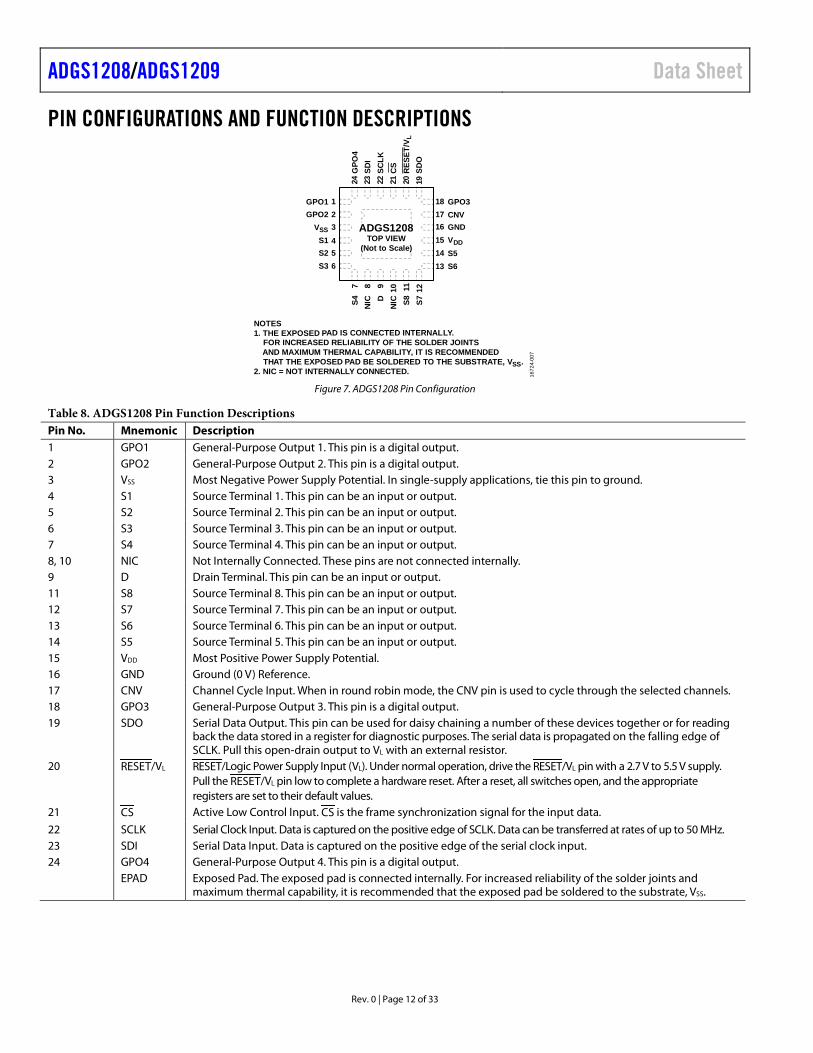
PIN CONFIGURATIONS AND FUNCTION DESCRIPTIONS
1672
4-00
7
21
3456
181716151413S3
S2S1
VSS
GPO2GPO1
NOTES1. THE EXPOSED PAD IS CONNECTED INTERNALLY. FOR INCREASED RELIABILITY OF THE SOLDER JOINTS
AND MAXIMUM THERMAL CAPABILITY, IT IS RECOMMENDED THAT THE EXPOSED PAD BE SOLDERED TO THE SUBSTRATE, VSS.2. NIC = NOT INTERNALLY CONNECTED.
S6S5VDD
GNDCNVGPO3
8 9 10 117N
IC DN
IC S812
S7S4
20 1921R
ESET
/VL
SDO
CS
22SC
LK23
SDI
24G
PO4
ADGS1208TOP VIEW
(Not to Scale)
Figure 7. ADGS1208 Pin Configuration
Table 8. ADGS1208 Pin Function Descriptions Pin No. Mnemonic Description 1 GPO1 General-Purpose Output 1. This pin is a digital output. 2 GPO2 General-Purpose Output 2. This pin is a digital output. 3 VSS Most Negative Power Supply Potential. In single-supply applications, tie this pin to ground. 4 S1 Source Terminal 1. This pin can be an input or output. 5 S2 Source Terminal 2. This pin can be an input or output. 6 S3 Source Terminal 3. This pin can be an input or output. 7 S4 Source Terminal 4. This pin can be an input or output. 8, 10 NIC Not Internally Connected. These pins are not connected internally. 9 D Drain Terminal. This pin can be an input or output. 11 S8 Source Terminal 8. This pin can be an input or output. 12 S7 Source Terminal 7. This pin can be an input or output. 13 S6 Source Terminal 6. This pin can be an input or output. 14 S5 Source Terminal 5. This pin can be an input or output. 15 VDD Most Positive Power Supply Potential. 16 GND Ground (0 V) Reference. 17 CNV Channel Cycle Input. When in round robin mode, the CNV pin is used to cycle through the selected channels. 18 GPO3 General-Purpose Output 3. This pin is a digital output. 19 SDO Serial Data Output. This pin can be used for daisy chaining a number of these devices together or for reading
back the data stored in a register for diagnostic purposes. The serial data is propagated on the falling edge of SCLK. Pull this open-drain output to VL with an external resistor.
20 RESET/VL RESET/Logic Power Supply Input (VL). Under normal operation, drive the RESET/VL pin with a 2.7 V to 5.5 V supply. Pull the RESET/VL pin low to complete a hardware reset. After a reset, all switches open, and the appropriate registers are set to their default values.
21 CS Active Low Control Input. CS is the frame synchronization signal for the input data.
22 SCLK Serial Clock Input. Data is captured on the positive edge of SCLK. Data can be transferred at rates of up to 50 MHz. 23 SDI Serial Data Input. Data is captured on the positive edge of the serial clock input. 24 GPO4 General-Purpose Output 4. This pin is a digital output. EPAD Exposed Pad. The exposed pad is connected internally. For increased reliability of the solder joints and
maximum thermal capability, it is recommended that the exposed pad be soldered to the substrate, VSS.
Data Sheet ADGS1208/ADGS1209
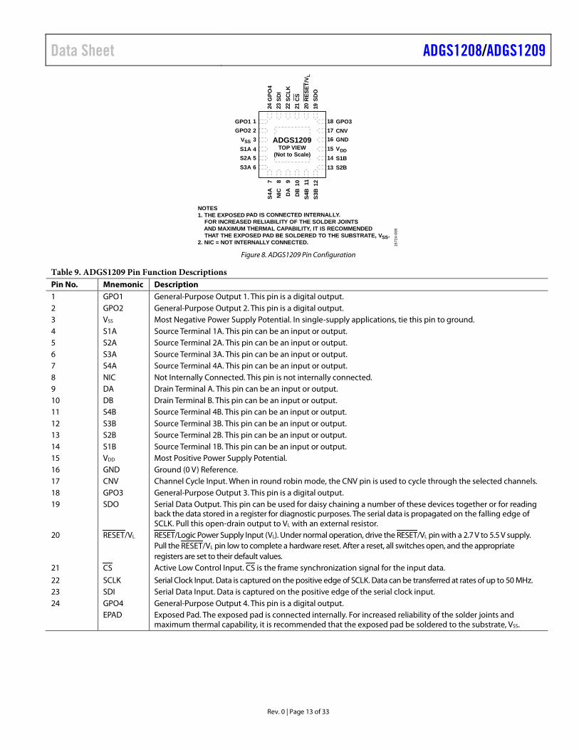
Rev. 0 | Page 13 of 33
1672
4-00
8
21
3456
181716151413S3A
S2AS1AVSS
GPO2GPO1
NOTES1. THE EXPOSED PAD IS CONNECTED INTERNALLY. FOR INCREASED RELIABILITY OF THE SOLDER JOINTS
AND MAXIMUM THERMAL CAPABILITY, IT IS RECOMMENDED THAT THE EXPOSED PAD BE SOLDERED TO THE SUBSTRATE, VSS.2. NIC = NOT INTERNALLY CONNECTED.
S2BS1BVDD
GNDCNVGPO3
8 9 10 117N
IC DA
DB
S4B
12S3
B
S4A
20 1921R
ESET
/VL
SDO
CS
22SC
LK23
SDI
24G
PO4
ADGS1209TOP VIEW
(Not to Scale)
Figure 8. ADGS1209 Pin Configuration
Table 9. ADGS1209 Pin Function Descriptions Pin No. Mnemonic Description 1 GPO1 General-Purpose Output 1. This pin is a digital output. 2 GPO2 General-Purpose Output 2. This pin is a digital output. 3 VSS Most Negative Power Supply Potential. In single-supply applications, tie this pin to ground. 4 S1A Source Terminal 1A. This pin can be an input or output. 5 S2A Source Terminal 2A. This pin can be an input or output. 6 S3A Source Terminal 3A. This pin can be an input or output. 7 S4A Source Terminal 4A. This pin can be an input or output. 8 NIC Not Internally Connected. This pin is not internally connected. 9 DA Drain Terminal A. This pin can be an input or output. 10 DB Drain Terminal B. This pin can be an input or output. 11 S4B Source Terminal 4B. This pin can be an input or output. 12 S3B Source Terminal 3B. This pin can be an input or output. 13 S2B Source Terminal 2B. This pin can be an input or output. 14 S1B Source Terminal 1B. This pin can be an input or output. 15 VDD Most Positive Power Supply Potential. 16 GND Ground (0 V) Reference. 17 CNV Channel Cycle Input. When in round robin mode, the CNV pin is used to cycle through the selected channels. 18 GPO3 General-Purpose Output 3. This pin is a digital output. 19 SDO Serial Data Output. This pin can be used for daisy chaining a number of these devices together or for reading
back the data stored in a register for diagnostic purposes. The serial data is propagated on the falling edge of SCLK. Pull this open-drain output to VL with an external resistor.
20 RESET/VL RESET/Logic Power Supply Input (VL). Under normal operation, drive the RESET/VL pin with a 2.7 V to 5.5 V supply. Pull the RESET/VL pin low to complete a hardware reset. After a reset, all switches open, and the appropriate registers are set to their default values.
21 CS Active Low Control Input. CS is the frame synchronization signal for the input data.
22 SCLK Serial Clock Input. Data is captured on the positive edge of SCLK. Data can be transferred at rates of up to 50 MHz. 23 SDI Serial Data Input. Data is captured on the positive edge of the serial clock input. 24 GPO4 General-Purpose Output 4. This pin is a digital output. EPAD Exposed Pad. The exposed pad is connected internally. For increased reliability of the solder joints and
maximum thermal capability, it is recommended that the exposed pad be soldered to the substrate, VSS.
ADGS1208/ADGS1209 Data Sheet
Rev. 0 | Page 14 of 33
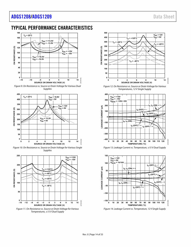
TYPICAL PERFORMANCE CHARACTERISTICS
SOURCE OR DRAIN VOLTAGE (V)
ON
RE
SIS
TA
NC
E (Ω
)
180
60
0–15 –10 –5 100 5 15
140
100
160
120
80
40
20
TA = 25°C
1672
4-03
1
VDD = +15VVSS = –15V
VDD = +13.5VVSS = –13.5V
VDD = +16.5VVSS = –16.5V
Figure 9. On Resistance vs. Source or Drain Voltage for Various Dual Supplies
SOURCE OR DRAIN VOLTAGE (V)
ON
RE
SIS
TA
NC
E (Ω
)
450
250
300
00 2 4 6 128 10 14
400
350
150
200
100
50
TA = 25°C
VDD = 12VVSS = 0V
VDD = 13.2VVSS = 0V
VDD = 10.8VVSS = 0V
1672
4-03
2
Figure 10. On Resistance vs. Source or Drain Voltage for Various Single Supplies
SOURCE OR DRAIN VOLTAGE (V)
ON
RE
SIS
TA
NC
E (Ω
)
250
0
150
200
100
50
1672
4-03
3
–15 –12 –9 –6 –3 0 3 6 9 12 15
TA = +25°C
TA = +85°C
TA = +125°C
TA = –40°C
VDD = +15VVSS = –15V
Figure 11. On Resistance vs. Source or Drain Voltage for Various Temperatures, ±15 V Dual Supply
SOURCE OR DRAIN VOLTAGE (V)
ON
RE
SIS
TA
NC
E (Ω
)
500
00 2 4 106 8 12
200
300
100
400
450
150
250
350
50
1672
4-03
4
TA = +125°C
TA = +85°C
VDD = 12VVSS = 0V
TA = +25°C
TA = –40°C
Figure 12. On Resistance vs. Source or Drain Voltage for Various Temperatures, 12 V Single Supply
400
–4000 10 20 30 40 50 60 70 80 90 100 110 120
TEMPERATURE (°C)
LE
AK
AG
E C
UR
RE
NT
(p
A)
300
200
100
0
–100
–200
–300
IS (OFF) + –
ID (OFF) + –
ID, IS (ON) + +
IS (OFF) – +
ID, IS (ON) – –
ID (OFF) – +
VDD = +15VVSS = –15VVBIAS = +10V/–10V
1672
4-05
7
Figure 13. Leakage Current vs. Temperature, ±15 V Dual Supply
150
–1500 10 20 30 40 50 60 70 80 90 100 110 120
TEMPERATURE (°C)
LE
AK
AG
E C
UR
RE
NT
(p
A)
100
50
0
–50
–100
IS (OFF) + –
ID (OFF) + –
IS (OFF) – +
ID (OFF) – +
ID, IS (ON) + +
ID, IS (ON) – –
VDD = 12VVSS = 0VVBIAS = 1V/10V
1672
4-05
8
Figure 14. Leakage Current vs. Temperature, 12 V Single Supply
Data Sheet ADGS1208/ADGS1209
Rev. 0 | Page 15 of 33
VS (V)
SOU
RC
E TO
DR
AIN
CH
AR
GE
INJE
CTI
ON
(pC
)
1.0
0–15 15
1672
4-04
0
0.9
0.8
0.7
0.6
0.5
0.4
0.3
0.2
0.1
–10 –5 0 5 10
MUX (SOURCE TO DRAIN)TA = 25°C
VDD = +15VVSS = –15V
VDD = +5VVSS = –5V
VDD = +12VVSS = 0V
Figure 15. Source to Drain Charge Injection vs. Source Voltage (VS)
VS (V)
SOU
RC
E TO
DR
AIN
CH
AR
GE
INJE
CTI
ON
(pC
)
6
–6–15 15
1672
4-04
1
–10 –5 0 5 10
DEMUX (DRAIN TO SOURCE)TA = 25°C
4
2
0
–2
–4
VDD = +15VVSS = –15V
VDD = +5VVSS = –5V
VDD = +12VVSS = 0V
Figure 16. Drain to Source Charge Injection vs. Source Voltage (VS)
0
20
40
60
80
100
120
140
160
180
200
–40 –20 0 20 40 60 80 100 120
t TR
AN
SITI
ON
(ns)
TEMPERATURE (°C)
15V DS12V SS
1672
4-01
8
Figure 17. Transition Time (tTRANSITION) vs. Temperature for Single Supply
(SS) and Dual Supply (DS)
1672
4-04
9
FREQUENCY (Hz)
OFF
ISO
LATI
ON
(dB
)
0
–10
–20
–30
–40
–50
–60
–70
–80
–90
–100
–11010k 100k 1M 10M 100M 1G
VDD = +15VVSS = –15VTA = 25°C
Figure 18. Off Isolation vs. Frequency, ±15 V Dual Supply
FREQUENCY (Hz)
CR
OSS
TALK
(dB
)
20
–12010k 1G
1672
4-04
2
100k 1M 10M 100M
0
–20
–40
–60
–80
–100
VDD = +15VVSS = –15VTA = 25°C
ADJACENT CHANNELS
NONADJACENTCHANNELS
Figure 19. ADGS1208 Crosstalk vs. Frequency, ±15 V Dual Supply
0
–12010k 1G
FREQUENCY (Hz)
CR
OSS
TALK
(dB
)
–20
–40
–60
–80
–100
100k 1M 10M 100M
ADJACENT CHANNELS
NONADJACENTCHANNELS
1672
4-05
3
VDD = +15VVSS = –15VTA = 25°C
Figure 20. ADGS1209 Crosstalk vs. Frequency, ±15 V Dual Supply
ADGS1208/ADGS1209 Data Sheet
Rev. 0 | Page 16 of 33
–130
–110
–90
–70
–50
–30
–10
10
100 1k 10k 100k 1M 10M
AC
PSR
R (d
B)
FREQUENCY (Hz)
100nF DECOUPLING CAPACITOR10µF + 100nF DECOUPLING CAPACITORNO DECOUPLING
TA = 25°CVDD = +15VVSS = –15V
1672
4-02
2
Figure 21. AC Power Supply Rejection Ratio (ACPSRR) vs. Frequency,
±15 V Dual Supply
FREQUENCY (Hz)
THD
+ N
(%)
10
1
0.1
0.0110 100 1k 10k 100k
LOAD = 10kΩTA = 25°C
VDD = +5V, VSS = –5V, VS = +3.5V rms
VDD = +15V, VSS = –15V, VS = +5V rms
1672
4-03
6
Figure 22. THD + N vs. Frequency
–20
–18
–16
–14
–12
–10
–8
–6
100 1k 10k 100k 1M 10M 100M 1G
INSE
RTI
ON
LO
SS (d
B)
FREQUENCY (Hz) 1672
4-12
4
TA = 25°CVDD = +15VVSS = –15V
Figure 23. ADGS1208 Insertion Loss vs. Frequency, ±15 V Dual Supply
–20
–18
–16
–14
–12
–10
–8
–6
100 1k 10k 100k 1M 10M 100M 1G
INSE
RTI
ON
LO
SS (d
B)
FREQUENCY (Hz) 1672
4-12
5
TA = 25°CVDD = +15VVSS = –15V
Figure 24. ADGS1209 Insertion Loss vs. Frequency, ±15 V Dual Supply
SOURCE VOLTAGE (V)
CA
PAC
ITA
NC
E (p
F)
0–15 15–10 –5 0 5 10
8
5
4
2
1
7
6
3
1672
4-04
3
VDD = +15VVSS = –15VTA = 25°C
SOURCE/DRAIN ON
DRAIN OFF
SOURCE OFF
Figure 25. ADG1208 Capacitance vs. Source Voltage, ±15 V Dual Supply
SOURCE VOLTAGE (V)
CA
PAC
ITA
NC
E (p
F)
0
8
5
4
2
1
7
6
3
1672
4-04
5
0 1 2 3 4 5 6 7 8 9 10 11 12
VDD = +12VVSS = 0VTA = 25°C
SOURCE/DRAIN ON
DRAIN OFF
SOURCE OFF
Figure 26. ADG1208 Capacitance vs. Source Voltage,
12 V Single Supply
Data Sheet ADGS1208/ADGS1209
Rev. 0 | Page 17 of 33
0 1 2 3 4 5 6 7 8 9 10 11 12SOURCE VOLTAGE (V)
CA
PAC
ITA
NC
E (p
F)
0
5
4
2
1
3
1672
4-04
7
VDD = +12VVSS = 0VTA = 25°C
SOURCE/DRAIN ON
DRAIN OFF
SOURCE OFF
Figure 27. ADG1209 Capacitance vs. Source Voltage, 12 V Single Supply
0–15 15
SOURCE VOLTAGE (V)
CA
PAC
ITA
NC
E (p
F)
–12 –9 –6 –3 0 3 6 9 12
SOURCE OFF
DRAIN OFF
SOURCE/DRAIN ON
5
4
3
2
1
1672
4-05
6
VDD = +15VVSS = –15VTA = 25°C
Figure 28. ADG1209 Capacitance vs. Source Voltage, ±15 V Dual Supply
-0.15
-0.10
-0.05
0
0.05
0.10
0.15
0.20
0 2 4 6 8
V OU
T (m
V)
TIME (µs)
SCLK = 2.5MHzSCLK IDLE
1672
4-13
1
Figure 29. Digital Feedthrough
0
50
100
150
200
250
300
I DD
(µA
)
2.7 3.0 3.5 4.0 4.5 5.0 5.5VL (V)
12V
15V
1672
4-23
2
TA = 25°CADGS1208 WITH S8 SLECTED
Figure 30. IDD vs. VL
0
50
100
150
200
250
300
350
400
450
1 10 20 30 40 50
I L (µ
A)
SCLK FREQUENCY (MHz)
TA = 25°C
1672
4-12
6
VL = 3V
VL = 5V
Figure 31. IL vs. SCLK Frequency when CS is High
ADGS1208/ADGS1209 Data Sheet
Rev. 0 | Page 18 of 33
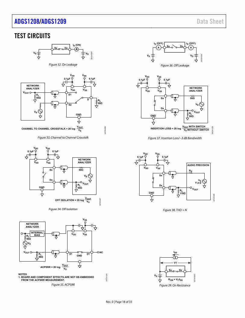
TEST CIRCUITS
VD
Sx Dx
VS
D (ON)
1672
4-02
4
Figure 32. On Leakage
CHANNEL TO CHANNEL CROSSTALK = 20 logVOUT
GND
S1
D
S2
VOUT
NETWORKANALYZER
RL50Ω
RL50Ω
VS
VS
VDD VSS
0.1µF
VDD
0.1µF
VSS
1672
4-02
6
Figure 33. Channel to Channel Crosstalk
OFF ISOLATION = 20 logVOUT
GND
Sx
Dx
VOUT
NETWORKANALYZER
RL50Ω
50Ω
VS
VS
VDD VSS
0.1µF
VDD
0.1µF
VSS
1672
4-02
7
Figure 34. Off Isolation
ACPSRR = 20 log
GNDD1S1
VOUT
VOUT
NETWORKANALYZER
RL50Ω
RL50Ω
VDD VSS
VSS
VS
NC
INTERNALBIAS
VS
NOTES1. BOARD AND COMPONENT EFFECTS ARE NOT DE-EMBEDDED FROM THE ACPSRR MEASUREMENT. 16
724-
141
Figure 35. ACPSRR
Sx Dx
VS
A A
VD
IS (OFF) ID (OFF)
1672
4-02
8
Figure 36. Off Leakage
INSERTION LOSS = 20 logVOUT WITH SWITCH
GND
Sx
Dx
VOUT
NETWORKANALYZER
RL50Ω
50Ω
VS
VS WITHOUT SWITCH
VDD VSS
0.1µF
VDD
0.1µF
VSS
1672
4-13
0
Figure 37. Insertion Loss/−3 dB Bandwidth
GND
Sx
Dx
VOUT
AUDIO PRECISION
RL110Ω
RS
VSV p-p
VDD VSS
0.1µF
VDD
0.1µF
VSS
1672
4-02
9
Figure 38. THD + N
Sx Dx
S
V1
IDS
RON = V1/IDS
1672
4-02
5
Figure 39. On Resistance
Data Sheet ADGS1208/ADGS1209
Rev. 0 | Page 19 of 33
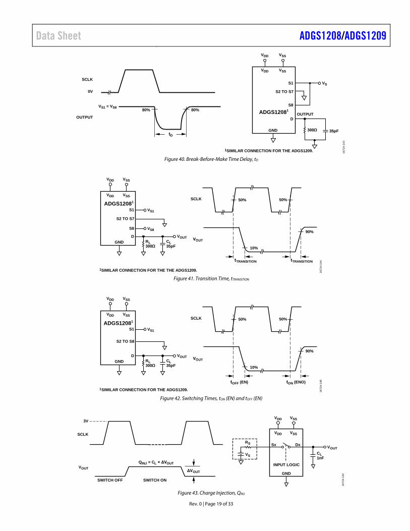
OUTPUTADGS12081
300ΩGND
S1
S2 TO S7
S8
D
35pF
VDD VSS
VDD VSS
VS
1SIMILAR CONNECTION FOR THE ADGS1209. 1672
4-14
3
0V
OUTPUT
80% 80%
tD
SCLK
VS1 = VS8
Figure 40. Break-Before-Make Time Delay, tD
VDD VSS
VDD VSS
GND RL300Ω
CL35pF
D VOUT
S8 VS8
S1ADGS12081
S2 TO S7
1SIMILAR CONNECTION FOR THE THE ADGS1209.
VS1
1672
4-14
4
50%
tTRANSITION tTRANSITION
10%
90%
50%SCLK
Figure 41. Transition Time, tTRANSITION
VDD VSS
VDD VSS
GND RL300Ω
CL35pF
D VOUT
S1
S2 TO S8
VS1
1672
4-14
550%
10%
90%
50%SCLKADGS12081
1SIMILAR CONNECTION FOR THE ADGS1209.
tOFF (EN) tON (ENO)
Figure 42. Switching Times, tON (EN) and tOFF (EN)
VDD VSS
VDD VSS
GND
INPUT LOGIC
CL1nF
Sx Dx VOUT
RS
VS
SCLK
3V
VOUT ΔVOUT
QINJ = CL × ΔVOUT
SWITCH OFF SWITCH ON
1672
4-13
2
Figure 43. Charge Injection, QINJ
ADGS1208/ADGS1209 Data Sheet
Rev. 0 | Page 20 of 33
VDD VSS
VDD VSS
GND
CL15pF
S1 VGPO
50%
tOFF (GPO) tON (GPO)
10%
90%
50%SCLK
1672
4-14
6
ADGS12081
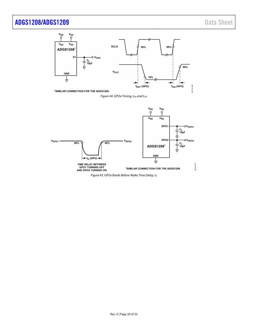
1SIMILAR CONNECTION FOR THE ADGS1209. Figure 44. GPOx Timing, tON and tOFF
ADGS12081
GND
GPO1
GPO2
VDD VSS
VDD VSS
1SIMILAR CONNECTION FOR THE ADGS1209.
1672
4-14
7
80%
TIME DELAY BETWEENGPO1 TURNING OFF
AND GPO2 TURNING ON
80%
tD (GPO)
VGPO1 VGPO2
CL15pF
VGPO1
CL15pF
VGPO2
Figure 45. GPOx Break-Before-Make Time Delay, tD
Data Sheet ADGS1208/ADGS1209
Rev. 0 | Page 21 of 33
TERMINOLOGY IDD IDD is the positive supply current.
ISS ISS is the negative supply current.
VD, VS VD and VS are the analog voltage on Terminal Dx and Terminal Sx, respectively.
RON RON is the ohmic resistance between Terminal Dx and Terminal Sx.
∆RON ∆RON is the difference between the RON of any two channels.
RFLAT (ON)
RFLAT (ON) is flatness that is the difference between maximum and minimum on resistance values measured over the specified analog signal range.
IS (Off) IS (Off) is the source leakage current with the switch off.
ID (Off) ID (Off) is the drain leakage current with the switch off.
IS (On), ID (On) IS (On) and ID (On) are the channel leakage currents with the switch on.
VINL VINL is the maximum input voltage for Logic 0.
VINH VINH is the minimum input voltage for Logic 1.
IINL, IINH IINL and IINH are the low and high input currents of the digital inputs, respectively.
CS (Off) CS (Off) is the off switch source capacitance, which is measured with reference to ground.
CD (Off) CD (Off) is the off switch drain capacitance, which is measured with reference to ground.
CS (On), CD (On) CS (On) and CD (On) are the on switch capacitances, which are measured with reference the ground.
CIN CIN is the digital input capacitance.
tON tON is the delay between applying the digital control input and the output switching on.
tOFF tOFF is the delay between applying the digital control input and the output switching off.
Off Isolation Off isolation is a measure of unwanted signal coupling through an off switch.
Charge Injection Charge injection is a measure of the glitch impulse transferred from the digital input to the analog output during switching.
Crosstalk Crosstalk is a measure of unwanted signal that is coupled through from one channel to another as a result of parasitic capacitance.
−3 dB Bandwidth Bandwidth is the frequency at which the output is attenuated by 3 dB.
On Response On response is the frequency response of the on switch.
Insertion Loss Insertion loss is the loss due to the on resistance of the switch.
Total Harmonic Distortion + Noise (THD + N) THD + N is the ratio of the harmonic amplitude plus noise of the signal to the fundamental.
AC Power Supply Rejection Ratio (ACPSRR) ACPSRR is the ratio of the amplitude of signal on the output to the amplitude of the modulation. ACPSRR is a measure of the ability of the devices to avoid coupling noise and spurious signals that appear on the supply voltage pin to the output of the switch. The dc voltage on the device is modulated by a sine wave of 0.62 V p-p.
ADGS1208/ADGS1209 Data Sheet
Rev. 0 | Page 22 of 33
THEORY OF OPERATION The ADGS1208/ADGS1209 are a set of serially controlled analog multiplexers comprising eight single channels and four differential channels, respectively, with error detection features. SPI Mode 0 and SPI Mode 3 can be used with the devices, and they operate with SCLK frequencies up to 50 MHz. The default mode for the ADGS1208/ADGS1209 is address mode, in which the registers of the device are accessed by a 16-bit SPI command bounded by CS. The SPI command becomes 24-bit if the user enables CRC error detection. Other error detection features include SCLK count error and invalid read/write error. If any of these SPI interface errors occur, they are detectable by reading the error flags register. The ADGS1208/ADGS1209 can also operate in two other modes, namely burst mode and daisy-chain mode.
The interface pins of the ADGS1208/ADGS1209 are CS, SCLK, SDI, and SDO. Hold CS low when using the SPI interface. Data is captured on SDI on the rising edge of SCLK, and data is propagated out on SDO on the falling edge of SCLK. SDO has an open-drain output; thus, connect a pull-up to this output. When not pulled low by the ADGS1208/ADGS1209, SDO is in a high impedance state.
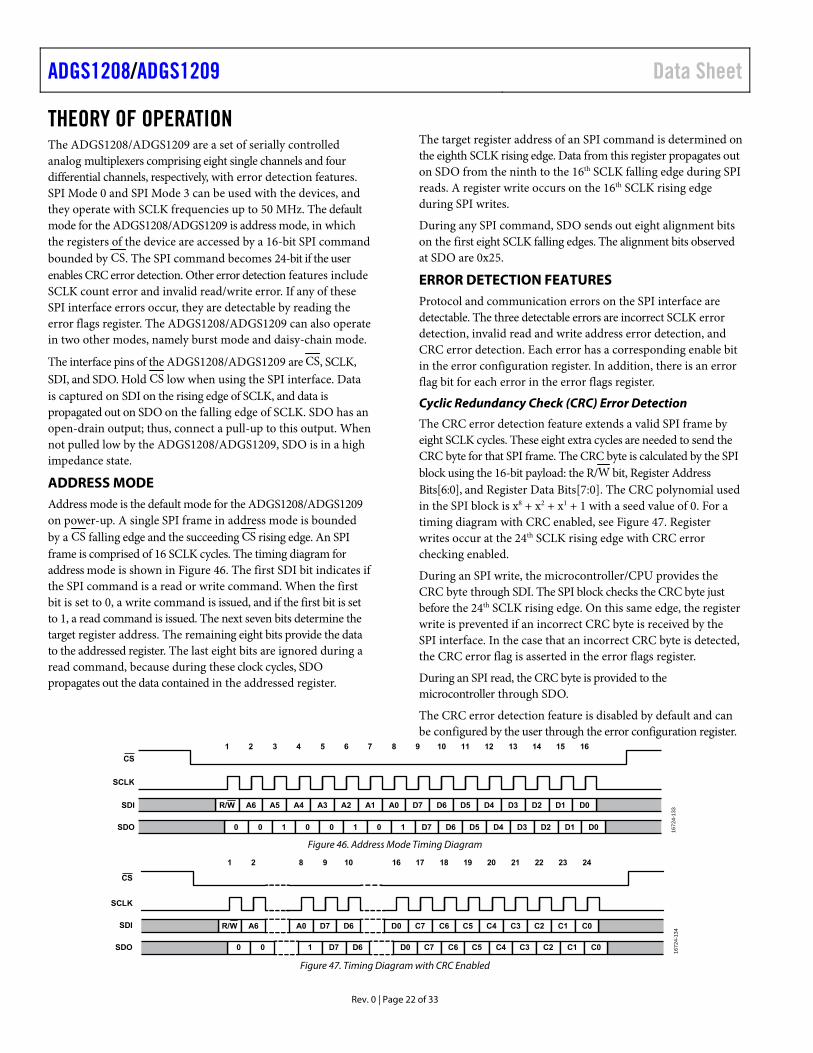
ADDRESS MODE Address mode is the default mode for the ADGS1208/ADGS1209 on power-up. A single SPI frame in address mode is bounded by a CS falling edge and the succeeding CS rising edge. An SPI frame is comprised of 16 SCLK cycles. The timing diagram for address mode is shown in Figure 46. The first SDI bit indicates if the SPI command is a read or write command. When the first bit is set to 0, a write command is issued, and if the first bit is set to 1, a read command is issued. The next seven bits determine the target register address. The remaining eight bits provide the data to the addressed register. The last eight bits are ignored during a read command, because during these clock cycles, SDO propagates out the data contained in the addressed register.
The target register address of an SPI command is determined on the eighth SCLK rising edge. Data from this register propagates out on SDO from the ninth to the 16th SCLK falling edge during SPI reads. A register write occurs on the 16th SCLK rising edge during SPI writes.
During any SPI command, SDO sends out eight alignment bits on the first eight SCLK falling edges. The alignment bits observed at SDO are 0x25.
ERROR DETECTION FEATURES Protocol and communication errors on the SPI interface are detectable. The three detectable errors are incorrect SCLK error detection, invalid read and write address error detection, and CRC error detection. Each error has a corresponding enable bit in the error configuration register. In addition, there is an error flag bit for each error in the error flags register.
Cyclic Redundancy Check (CRC) Error Detection
The CRC error detection feature extends a valid SPI frame by eight SCLK cycles. These eight extra cycles are needed to send the CRC byte for that SPI frame. The CRC byte is calculated by the SPI block using the 16-bit payload: the R/W bit, Register Address Bits[6:0], and Register Data Bits[7:0]. The CRC polynomial used in the SPI block is x8 + x2 + x1 + 1 with a seed value of 0. For a timing diagram with CRC enabled, see Figure 47. Register writes occur at the 24th SCLK rising edge with CRC error checking enabled.
During an SPI write, the microcontroller/CPU provides the CRC byte through SDI. The SPI block checks the CRC byte just before the 24th SCLK rising edge. On this same edge, the register write is prevented if an incorrect CRC byte is received by the SPI interface. In the case that an incorrect CRC byte is detected, the CRC error flag is asserted in the error flags register.
During an SPI read, the CRC byte is provided to the microcontroller through SDO.
The CRC error detection feature is disabled by default and can be configured by the user through the error configuration register.
0 0 1 0 0 1 0 1 D7 D6 D5 D4 D3 D2 D1 D0SDO
R/W A6 A5 A4 A3 A2 A1 A0 D7 D6 D5 D4 D3 D2 D1 D0
1 2 3 4 5 6 7 8 9 10 11 12 13 14 15 16
SDI
SCLK
CS
1672
4-13
3
Figure 46. Address Mode Timing Diagram
0 0 1 D7 D6 D0 C7 C6 C5 C4 C3 C2 C1 C0SDO
R/W A6 A0 D7 D6 D0 C7 C6 C5 C4 C3 C2 C1 C0
1 2 8 9 10 16 17 18 19 20 21 22 23 24
SDI
SCLK
CS
1672
4-13
4
Figure 47. Timing Diagram with CRC Enabled
Data Sheet ADGS1208/ADGS1209
Rev. 0 | Page 23 of 33
SCLK Count Error Detection
SCLK count error detection allows the user to detect if an incorrect number of SCLK cycles are sent by the microcontroller/ CPU. When in address mode, with CRC disabled, 16 SCLK cycles are expected. If 16 SCLK cycles are not detected, the SCLK count error flag asserts in the error flags register. When less than 16 SCLK cycles are received by the device, a write to the register map never occurs. When the ADGS1208/ADGS1209 receive more than 16 SCLK cycles, a write to the memory map still occurs at the 16th SCLK rising edge, and the flag asserts in the error flags register. With CRC enabled, the expected number of SCLK cycles is 24. SCLK count error detection is enabled by default and can be configured by the user through the error configuration register.
Invalid Read/Write Address Error Detection
An invalid read/write address error detects when a nonexistent register address is a target for a read or write. In addition, this error asserts when a write to a read only register is attempted. The invalid read/write address error flag asserts in the error flags register when an invalid read/write address error occurs. The invalid read/write address error is detected on the ninth SCLK rising edge, which means a write to the register never occurs when an invalid address is targeted. Invalid read/write address error detection is enabled by default and can be disabled by the user through the error configuration register.
CLEARING THE ERROR FLAGS REGISTER To clear the error flags register, write the special 16-bit SPI frame, 0x6CA9, to the device. This SPI command does not trigger the invalid read/write address error. When CRC is enabled, the user must also send the correct CRC byte for a successful error clear command. At the 16th or 24th SCLK rising edge, the error flags register resets to 0.
BURST MODE The SPI interface can accept consecutive SPI commands without the need to de-assert the CS line, which is called burst mode. Burst mode is enabled through the burst enable register. This mode uses the same 16-bit command to communicate with the device. In addition, the response of the device at SDO is still aligned with the corresponding SPI command. Figure 48 shows an example of SDI and SDO during burst mode.
The invalid read/write address and CRC error checking functions operate similarly during burst mode as they do during address mode. However, SCLK count error detection operates in a slightly different manner. The total number of SCLK cycles within a given CS frame are counted, and if the total is not a multiple of 16, or a multiple of 24 when CRC is enabled, the SCLK count error flag asserts.
SDO
COMMAND0[15:0]
RESPONSE0[15:0]
COMMAND1[15:0]
RESPONSE1[15:0]
COMMAND2[15:0]
RESPONSE2[15:0]
COMMAND3[15:0]
RESPONSE3[15:0]
SDI
CS
1672
4-13
5
Figure 48. Burst Mode Frame
SOFTWARE RESET When in address mode, the user can initiate a software reset. To do so, write two consecutive SPI commands, 0xA3 followed by 0x05, targeting Register 0x0B. After a software reset, all register values are set to default.
DAISY-CHAIN MODE The connection of several ADGS1208/ADGS1209 devices in a daisy chain configuration is possible, and Figure 49 shows this setup. All devices share the same CS and SCLK line, whereas the SDO of a device forms a connection to the SDI of the next device, creating a shift register. In daisy-chain mode, SDO is an eight cycle delayed version of SDI. When in daisy-chain mode, all commands target the switch data register. Therefore, it is not possible to make configuration changes while in daisy-chain mode.
S8
SDISCLK
CSRESET/VL
S1
SDO
VL
D
ADGS1208DEVICE 1
SDO
ADGS1208DEVICE 2
SPIINTERFACE
SPIINTERFACE
1672
4-05
0
S8
S1
D
Figure 49. Two ADGS1208/ADGS1209 Devices Connected in a Daisy-Chain Configuration
ADGS1208/ADGS1209 Data Sheet
Rev. 0 | Page 24 of 33
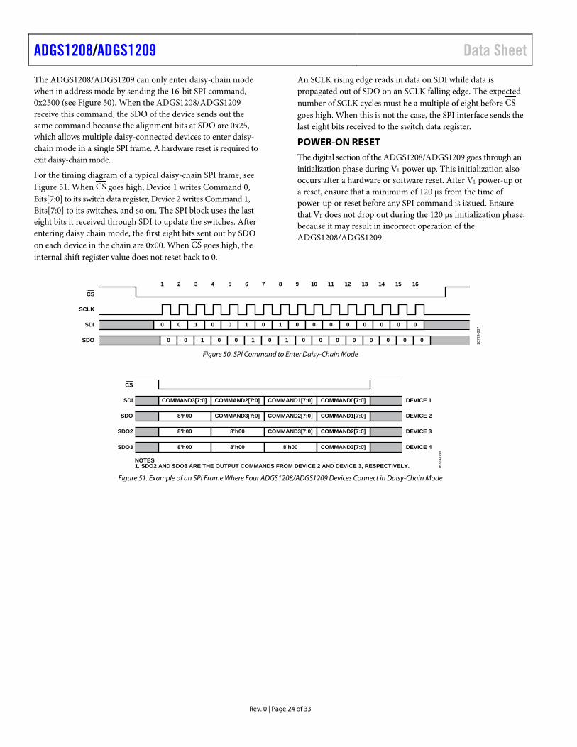
The ADGS1208/ADGS1209 can only enter daisy-chain mode when in address mode by sending the 16-bit SPI command, 0x2500 (see Figure 50). When the ADGS1208/ADGS1209 receive this command, the SDO of the device sends out the same command because the alignment bits at SDO are 0x25, which allows multiple daisy-connected devices to enter daisy-chain mode in a single SPI frame. A hardware reset is required to exit daisy-chain mode.
For the timing diagram of a typical daisy-chain SPI frame, see Figure 51. When CS goes high, Device 1 writes Command 0, Bits[7:0] to its switch data register, Device 2 writes Command 1, Bits[7:0] to its switches, and so on. The SPI block uses the last eight bits it received through SDI to update the switches. After entering daisy chain mode, the first eight bits sent out by SDO on each device in the chain are 0x00. When CS goes high, the internal shift register value does not reset back to 0.
An SCLK rising edge reads in data on SDI while data is propagated out of SDO on an SCLK falling edge. The expected number of SCLK cycles must be a multiple of eight before CS goes high. When this is not the case, the SPI interface sends the last eight bits received to the switch data register.
POWER-ON RESET The digital section of the ADGS1208/ADGS1209 goes through an initialization phase during VL power up. This initialization also occurs after a hardware or software reset. After VL power-up or a reset, ensure that a minimum of 120 µs from the time of power-up or reset before any SPI command is issued. Ensure that VL does not drop out during the 120 µs initialization phase, because it may result in incorrect operation of the ADGS1208/ADGS1209.
0 0 1 0 0 1 0 1 0 0 0 0 0 0 0 0SDO
0 0 1 0 0 1 0 1 0 0 0 0 0 0 0 0
1 2 3 4 5 6 7 8 9 10 11 12 13 14 15 16
SDI
SCLK
CS
1672
4-03
7
Figure 50. SPI Command to Enter Daisy-Chain Mode
SDO
COMMAND3[7:0]
8’h00
COMMAND2[7:0]
COMMAND3[7:0]
COMMAND1[7:0]
COMMAND2[7:0]
COMMAND0[7:0]
COMMAND1[7:0]
SDI
SDO3
8’h00
8’h00
8’h00
8’h00
COMMAND3[7:0]
8’h00
COMMAND2[7:0]
COMMAND3[7:0]
SDO2
DEVICE 2
DEVICE 1
DEVICE 4
DEVICE 3
CS
NOTES1. SDO2 AND SDO3 ARE THE OUTPUT COMMANDS FROM DEVICE 2 AND DEVICE 3, RESPECTIVELY. 16
724-
038
Figure 51. Example of an SPI Frame Where Four ADGS1208/ADGS1209 Devices Connect in Daisy-Chain Mode
Data Sheet ADGS1208/ADGS1209
Rev. 0 | Page 25 of 33
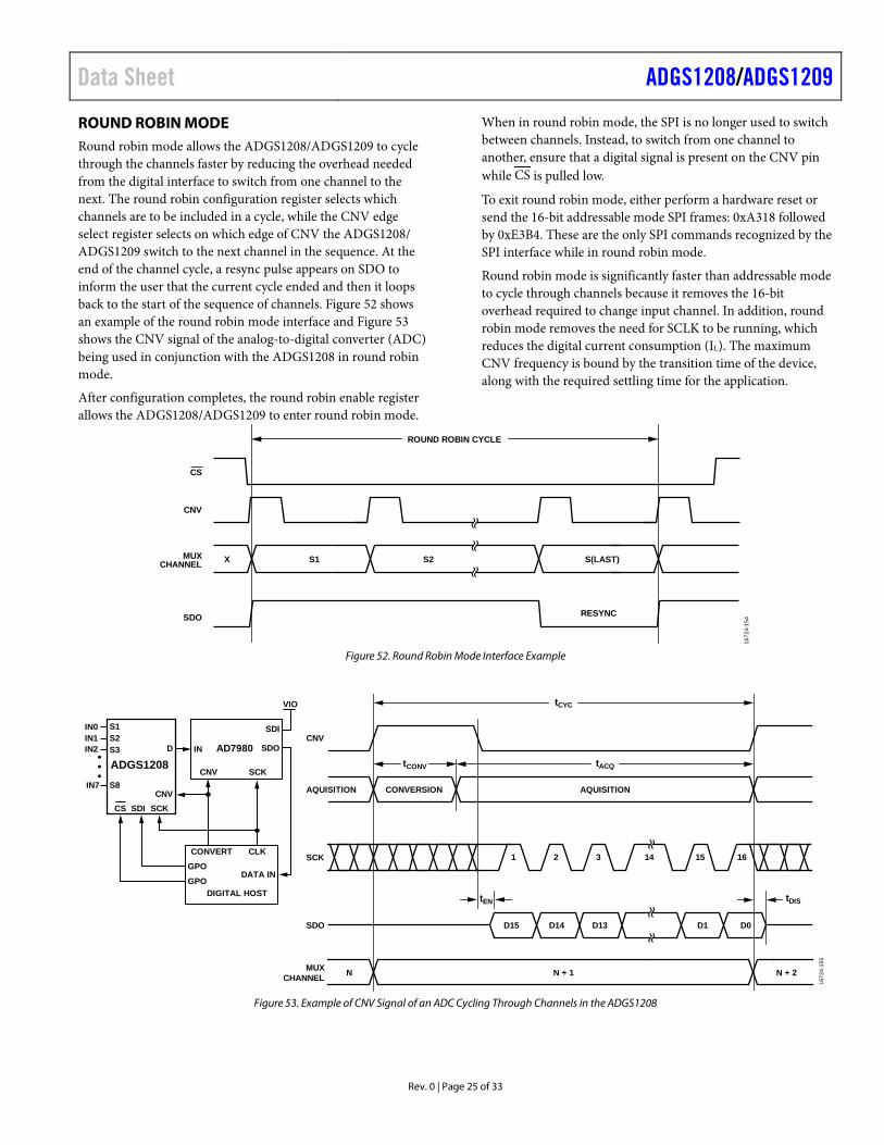
ROUND ROBIN MODE Round robin mode allows the ADGS1208/ADGS1209 to cycle through the channels faster by reducing the overhead needed from the digital interface to switch from one channel to the next. The round robin configuration register selects which channels are to be included in a cycle, while the CNV edge select register selects on which edge of CNV the ADGS1208/ ADGS1209 switch to the next channel in the sequence. At the end of the channel cycle, a resync pulse appears on SDO to inform the user that the current cycle ended and then it loops back to the start of the sequence of channels. Figure 52 shows an example of the round robin mode interface and Figure 53 shows the CNV signal of the analog-to-digital converter (ADC) being used in conjunction with the ADGS1208 in round robin mode.
After configuration completes, the round robin enable register allows the ADGS1208/ADGS1209 to enter round robin mode.
When in round robin mode, the SPI is no longer used to switch between channels. Instead, to switch from one channel to another, ensure that a digital signal is present on the CNV pin while CS is pulled low.
To exit round robin mode, either perform a hardware reset or send the 16-bit addressable mode SPI frames: 0xA318 followed by 0xE3B4. These are the only SPI commands recognized by the SPI interface while in round robin mode.
Round robin mode is significantly faster than addressable mode to cycle through channels because it removes the 16-bit overhead required to change input channel. In addition, round robin mode removes the need for SCLK to be running, which reduces the digital current consumption (IL). The maximum CNV frequency is bound by the transition time of the device, along with the required settling time for the application.
CNV
MUXCHANNEL X S1 S2 S(LAST)
ROUND ROBIN CYCLE
SDO RESYNC
CS
1672
4-15
4
Figure 52. Round Robin Mode Interface Example
1672
4-15
5
CNV
AQUISITION AQUISITION
tACQ
tCYC
tCONV
tDIStEN
CONVERSION
SCK
SDO
MUXCHANNEL
D15 D14
N + 2N + 1N
D13 D1 D0
1 2 3 14 15 16
AD7980 SDO
SDI
SDI
DATA IN
DIGITAL HOST
CLK
VIO
CNV SCK
CONVERT
IN0IN1IN2
IN7
ADGS1208
SCKCS
GPO
GPO
CNV
D IN
S1S2
S8
S3
Figure 53. Example of CNV Signal of an ADC Cycling Through Channels in the ADGS1208
ADGS1208/ADGS1209 Data Sheet
Rev. 0 | Page 26 of 33
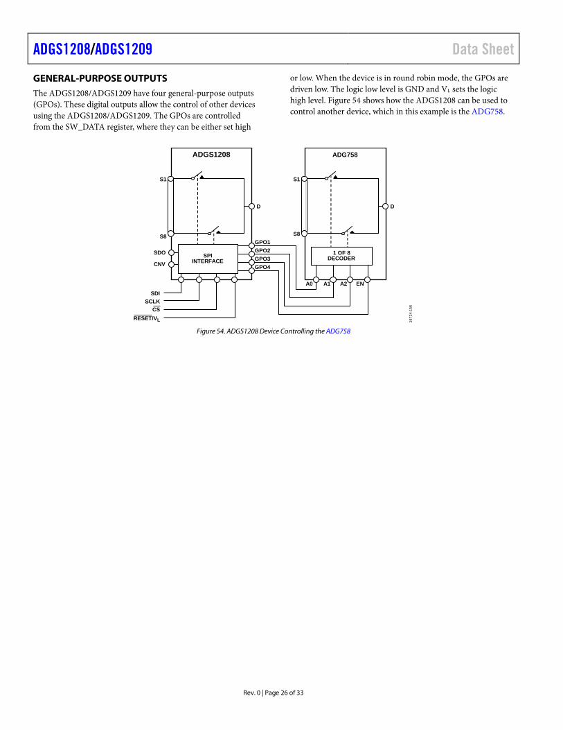
GENERAL-PURPOSE OUTPUTS The ADGS1208/ADGS1209 have four general-purpose outputs (GPOs). These digital outputs allow the control of other devices using the ADGS1208/ADGS1209. The GPOs are controlled from the SW_DATA register, where they can be either set high
or low. When the device is in round robin mode, the GPOs are driven low. The logic low level is GND and VL sets the logic high level. Figure 54 shows how the ADGS1208 can be used to control another device, which in this example is the ADG758.
S8
SDISCLK
CSRESET/VL
S1
GPO1
A0 A1 A2 EN
D
ADGS1208
SDO
CNV
ADG758
GPO2GPO3GPO4
1 OF 8DECODER
1672
4-15
6
S8
S1
D
SPIINTERFACE
Figure 54. ADGS1208 Device Controlling the ADG758
Data Sheet ADGS1208/ADGS1209
Rev. 0 | Page 27 of 33
APPLICATIONS INFORMATION DIGITAL INPUT BUFFERS There are input buffers present on the digital input pins (CS, SCLK, and SDI). These buffers are active at all times; as result, there is current draw from the VL supply if SCLK or SDI are toggling, regardless of whether CS is active. For typical values of this current draw, refer to the Specifications section and Figure 31.
SETTLING TIME Disturbances are apparent on the source/drain when switching between channels, as is typical with complementary metal-oxide semiconductor (CMOS) switches and multiplexers. A sufficient wait time is necessary for these disturbances to settle before taking a measurement to ensure an accurate reading. The settling time for a data acquisition system is dependent on the load on the output of the multiplexer.
POWER SUPPLY RAILS To guarantee correct operation of the ADGS1208/ADGS1209, 0.1 µF decoupling capacitors are required.
The ADGS1208/ADGS1209 can operate with bipolar supplies between ±4.5 V and ±16.5 V. The supplies on VDD and VSS do not need to be symmetrical. However, the VDD to VSS range must not exceed 33 V. The ADGS1208/ADGS1209 can also operate with single supplies between 5 V and 20 V with VSS connected to GND.
The voltage range that can be supplied to VL is from 2.7 V to 5.5 V.
The device is fully specified at ±15 V and +12 V analog supply voltage ranges.
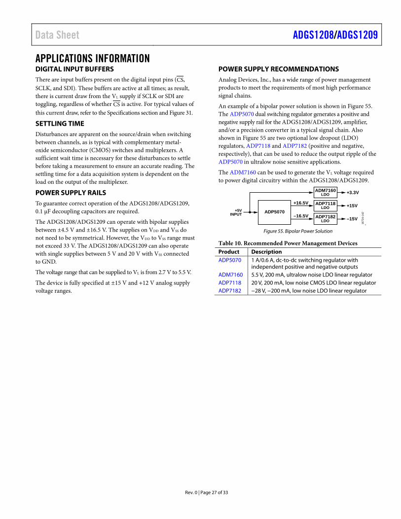
POWER SUPPLY RECOMMENDATIONS Analog Devices, Inc., has a wide range of power management products to meet the requirements of most high performance signal chains.
An example of a bipolar power solution is shown in Figure 55. The ADP5070 dual switching regulator generates a positive and negative supply rail for the ADGS1208/ADGS1209, amplifier, and/or a precision converter in a typical signal chain. Also shown in Figure 55 are two optional low dropout (LDO) regulators, ADP7118 and ADP7182 (positive and negative, respectively), that can be used to reduce the output ripple of the ADP5070 in ultralow noise sensitive applications.
The ADM7160 can be used to generate the VL voltage required to power digital circuitry within the ADGS1208/ADGS1209.
1672
4-14
2
ADM7160LDO +3.3V
ADP7118LDO +15V
ADP7182LDO –15V
+16.5V
–16.5VADP5070+5V
INPUT
.
Figure 55. Bipolar Power Solution
Table 10. Recommended Power Management Devices Product Description ADP5070 1 A/0.6 A, dc-to-dc switching regulator with
independent positive and negative outputs ADM7160 5.5 V, 200 mA, ultralow noise LDO linear regulator ADP7118 20 V, 200 mA, low noise CMOS LDO linear regulator ADP7182 −28 V, −200 mA, low noise LDO linear regulator
ADGS1208/ADGS1209 Data Sheet
Rev. 0 | Page 28 of 33
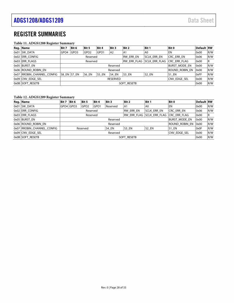
REGISTER SUMMARIES Table 11. ADGS1208 Register Summary Reg. Name Bit 7 Bit 6 Bit 5 Bit 4 Bit 3 Bit 2 Bit 1 Bit 0 Default RW
0x01 SW_DATA GPO4 GPO3 GPO2 GPO1 A2 A1 A0 EN 0x00 R/W
0x02 ERR_CONFIG Reserved RW_ERR_EN SCLK_ERR_EN CRC_ERR_EN 0x06 R/W
0x03 ERR_FLAGS Reserved RW_ERR_FLAG SCLK_ERR_FLAG CRC_ERR_FLAG 0x00 R
0x05 BURST_EN Reserved BURST_MODE_EN 0x00 R/W
0x06 ROUND_ROBIN_EN Reserved ROUND_ROBIN_EN 0x00 R/W
0x07 RROBIN_CHANNEL_CONFIG S8_EN S7_EN S6_EN S5_EN S4_EN S3_EN S2_EN S1_EN 0xFF R/W
0x09 CNV_EDGE_SEL RESERVED CNV_EDGE_SEL 0x00 R/W
0x0B SOFT_RESETB SOFT_RESETB 0x00 R/W
Table 12. ADGS1209 Register Summary Reg. Name Bit 7 Bit 6 Bit 5 Bit 4 Bit 3 Bit 2 Bit 1 Bit 0 Default RW
0x01 SW_DATA GPO4 GPO3 GPO2 GPO1 Reserved A1 A0 EN 0x00 R/W
0x02 ERR_CONFIG Reserved RW_ERR_EN SCLK_ERR_EN CRC_ERR_EN 0x06 R/W
0x03 ERR_FLAGS Reserved RW_ERR_FLAG SCLK_ERR_FLAG CRC_ERR_FLAG 0x00 R
0x05 BURST_EN Reserved BURST_MODE_EN 0x00 R/W
0x06 ROUND_ROBIN_EN Reserved ROUND_ROBIN_EN 0x00 R/W
0x07 RROBIN_CHANNEL_CONFIG Reserved S4_EN S3_EN S2_EN S1_EN 0x0F R/W
0x09 CNV_EDGE_SEL Reserved CNV_EDGE_SEL 0x00 R/W
0x0B SOFT_RESETB SOFT_RESETB 0x00 R/W
Data Sheet ADGS1208/ADGS1209
Rev. 0 | Page 29 of 33
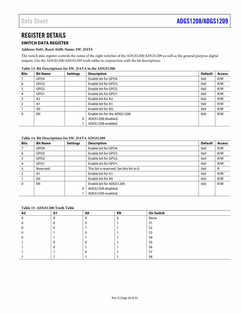
REGISTER DETAILS SWITCH DATA REGISTER Address: 0x01, Reset: 0x00, Name: SW_DATA
The switch data register controls the status of the eight switches of the ADGS1208/ADGS1209 as well as the general-purpose digital outputs. Use the ADGS1208/ADGS1209 truth tables in conjunction with the bit descriptions.
Table 13. Bit Descriptions for SW_DATA in the ADGS1208 Bits Bit Name Settings Description Default Access 7 GPO4 Enable bit for GPO4. 0x0 R/W 6 GPO3 Enable bit for GPO3. 0x0 R/W 5 GPO2 Enable bit for GPO2. 0x0 R/W 4 GPO1 Enable bit for GPO1. 0x0 R/W 3 A2 Enable bit for A2. 0x0 R/W 2 A1 Enable bit for A1. 0x0 R/W 1 A0 Enable bit for A0. 0x0 R/W 0 EN Enable bit for the ADGS1208. 0x0 R/W 0 ADGS1208 disabled. 1 ADGS1208 enabled.
Table 14. Bit Descriptions for SW_DATA ADGS1209 Bits Bit Name Settings Description Default Access 7 GPO4 Enable bit for GPO4. 0x0 R/W
6 GPO3 Enable bit for GPO3. 0x0 R/W
5 GPO2 Enable bit for GPO2. 0x0 R/W
4 GPO1 Enable bit for GPO1. 0x0 R/W
3 Reserved This bit is reserved. Set this bit to 0. 0x0 R 2 A1 Enable bit for A1. 0x0 R/W 1 A0 Enable bit for A0. 0x0 R/W 0 EN Enable bit for ADGS1209. 0x0 R/W 0 ADGS1209 disabled. 1 ADGS1209 enabled.
Table 15. ADGS1208 Truth Table A2 A1 A0 EN On Switch X X X 0 None 0 0 0 1 S1 0 0 1 1 S2 0 1 0 1 S3 0 1 1 1 S4 1 0 0 1 S5 1 0 1 1 S6 1 1 0 1 S7 1 1 1 1 S8
ADGS1208/ADGS1209 Data Sheet
Rev. 0 | Page 30 of 33
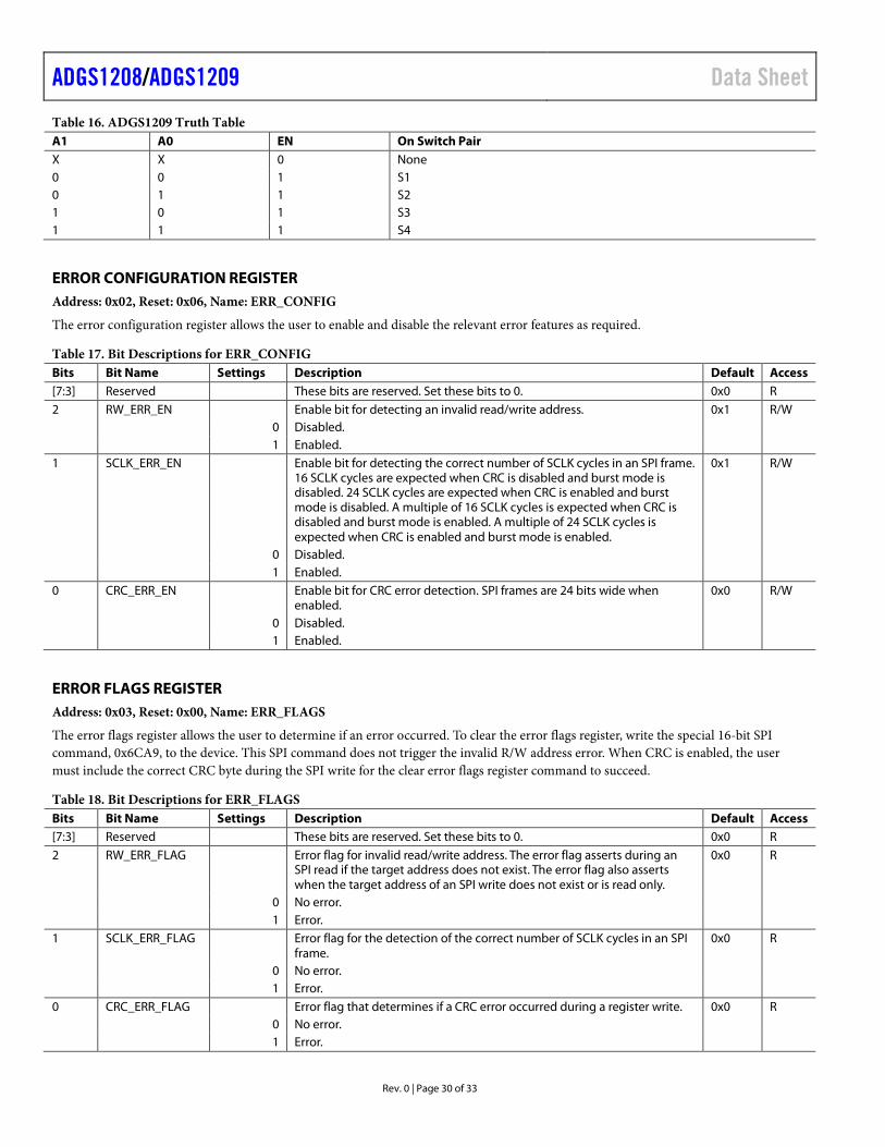
Table 16. ADGS1209 Truth Table A1 A0 EN On Switch Pair X X 0 None 0 0 1 S1 0 1 1 S2 1 0 1 S3 1 1 1 S4
ERROR CONFIGURATION REGISTER Address: 0x02, Reset: 0x06, Name: ERR_CONFIG
The error configuration register allows the user to enable and disable the relevant error features as required.
Table 17. Bit Descriptions for ERR_CONFIG Bits Bit Name Settings Description Default Access [7:3] Reserved These bits are reserved. Set these bits to 0. 0x0 R 2 RW_ERR_EN Enable bit for detecting an invalid read/write address. 0x1 R/W 0 Disabled. 1 Enabled. 1 SCLK_ERR_EN Enable bit for detecting the correct number of SCLK cycles in an SPI frame.
16 SCLK cycles are expected when CRC is disabled and burst mode is disabled. 24 SCLK cycles are expected when CRC is enabled and burst mode is disabled. A multiple of 16 SCLK cycles is expected when CRC is disabled and burst mode is enabled. A multiple of 24 SCLK cycles is expected when CRC is enabled and burst mode is enabled.
0x1 R/W
0 Disabled. 1 Enabled. 0 CRC_ERR_EN Enable bit for CRC error detection. SPI frames are 24 bits wide when
enabled. 0x0 R/W
0 Disabled. 1 Enabled.
ERROR FLAGS REGISTER Address: 0x03, Reset: 0x00, Name: ERR_FLAGS
The error flags register allows the user to determine if an error occurred. To clear the error flags register, write the special 16-bit SPI command, 0x6CA9, to the device. This SPI command does not trigger the invalid R/W address error. When CRC is enabled, the user must include the correct CRC byte during the SPI write for the clear error flags register command to succeed.
Table 18. Bit Descriptions for ERR_FLAGS Bits Bit Name Settings Description Default Access [7:3] Reserved These bits are reserved. Set these bits to 0. 0x0 R 2 RW_ERR_FLAG Error flag for invalid read/write address. The error flag asserts during an
SPI read if the target address does not exist. The error flag also asserts when the target address of an SPI write does not exist or is read only.
0x0 R
0 No error. 1 Error. 1 SCLK_ERR_FLAG Error flag for the detection of the correct number of SCLK cycles in an SPI
frame. 0x0 R
0 No error. 1 Error. 0 CRC_ERR_FLAG Error flag that determines if a CRC error occurred during a register write. 0x0 R 0 No error. 1 Error.
Data Sheet ADGS1208/ADGS1209
Rev. 0 | Page 31 of 33
BURST ENABLE REGISTER Address: 0x05, Reset: 0x00, Name: BURST_EN
The burst enable register allows the user to enable or disable burst mode. When enabled, the user can send multiple consecutive SPI commands without deasserting CS.
Table 19. Bit Descriptions for BURST_EN Bits Bit Name Settings Description Default Access [7:1] Reserved These bits are reserved. Set these bits to 0. 0x0 R 0 BURST_MODE_EN Burst mode enable bit. 0x0 R/W 0 Disabled. 1 Enabled.
ROUND ROBIN ENABLE REGISTER Address: 0x06, Reset: 0x00, Name: ROUND_ROBIN_EN
The round robin register allows the user to enable or disable round robin mode. When enabled, the user can cycle through the channels enabled in the round robin configuration register by presenting the relevant edge on the CNV pin.
Table 20. Bit Descriptions for ROUND_ROBIN_EN Bits Bit Name Settings Description Default Access [7:1] Reserved These bits are reserved. Set these bits to 0. 0x0 R 0 ROUND_ROBIN_EN Round robin mode enable bit. 0x0 R/W 0 Disabled. 1 Enabled.
ROUND ROBIN CHANNEL CONFIGURATION REGISTER Address: 0x07, Reset: 0xFF (ADGS1208), 0x0F (ADGS1209), Name: RROBIN_CHANNEL_CONFIG
The round robin channel configuration register controls which channels are included a cycle during round robin mode. During round robin mode, the channels are cycled through in ascending order.
Table 21. Bit Descriptions for RROBIN_CHANNEL_CONFIG (ADGS1208) Bits Bit Name Settings Description Default Access 7 S8_EN Enable bit for S8. 0x1 R/W 0 S8 disabled during round robin mode. 1 S8 enabled during round robin mode. 6 S7_EN Enable bit for S7. 0x1 R/W 0 S7 disabled during round robin mode. 1 S7 enabled during round robin mode. 5 S6_EN Enable bit for S6. 0x1 R/W 0 S6 disabled during round robin mode. 1 S6 enabled during round robin mode. 4 S5_EN Enable bit for S5. 0x1 R/W 0 S5 disabled during round robin mode. 1 S5 enabled during round robin mode. 3 S4_EN Enable bit for S4. 0x1 R/W 0 S4 disabled during round robin mode. 1 S4 enabled during round robin mode. 2 S3_EN Enable bit for S3. 0x1 R/W 0 S3 disabled during round robin mode. 1 S3 enabled during round robin mode.
ADGS1208/ADGS1209 Data Sheet
Rev. 0 | Page 32 of 33
Bits Bit Name Settings Description Default Access 1 S2_EN Enable bit for S2. 0x1 R/W 0 S2 disabled during round robin mode. 1 S2 enabled during round robin mode. 0 S1_EN Enable bit for S1. 0x1 R/W 0 S1 disabled during round robin mode. 1 S1 enabled during round robin mode.
Table 22. Bit Descriptions for RROBIN_CHANNEL_CONFIG (ADGS1209) Bits Bit Name Settings Description Default Access [7:4] Reserved These bits are reserved. Set these bits to 0. 0x0 R 3 S4_EN Enable bit for S4. 0x1 R/W 0 S4 disabled during round robin mode. 1 S4 enabled during round robin mode. 2 S3_EN Enable bit for S3. 0x1 R/W 0 S3 disabled during round robin mode. 1 S3 enabled during round robin mode. 1 S2_EN Enable bit for S2. 0x1 R/W 0 S2 disabled during round robin mode. 1 S2 enabled during round robin mode. 0 S1_EN Enable bit for S1. 0x1 R/W 0 S1 disabled during round robin mode. 1 S1 enabled during round robin mode.
CNV EDGE SELECT REGISTER Address: 0x09, Reset: 0x00, Name: CNV_EDGE_SEL
The CNV edge select register allows the user to select the active edge of the CNV pin when the device is in round robin mode.
Table 23. Bit Descriptions for CNV_EDGE_SEL Bits Bit Name Settings Description Default Access [7:1] Reserved These bits are reserved. Set these bits to 0. 0x0 R 0 CNV_EDGE_SEL CNV active edge select bit. 0x0 R/W 0 Falling edge of CNV is the active edge. 1 Rising edge of CNV is the active edge.
SOFTWARE RESET REGISTER Address: 0x0B, Reset: 0x00, Name: SOFT_RESETB
Use the software reset register to perform a software reset. Consecutively, write 0xA3 followed by 0x05 to this register, and the registers of the device reset to their default state.
Table 24. Bit Descriptions for SOFT_RESETB Bits Bit Name Settings Description Default Access [7:0] SOFT_RESETB To perform a software reset, consecutively write 0xA3 followed by 0x05 to
this register. 0x0 R
Data Sheet ADGS1208/ADGS1209
Rev. 0 | Page 33 of 33
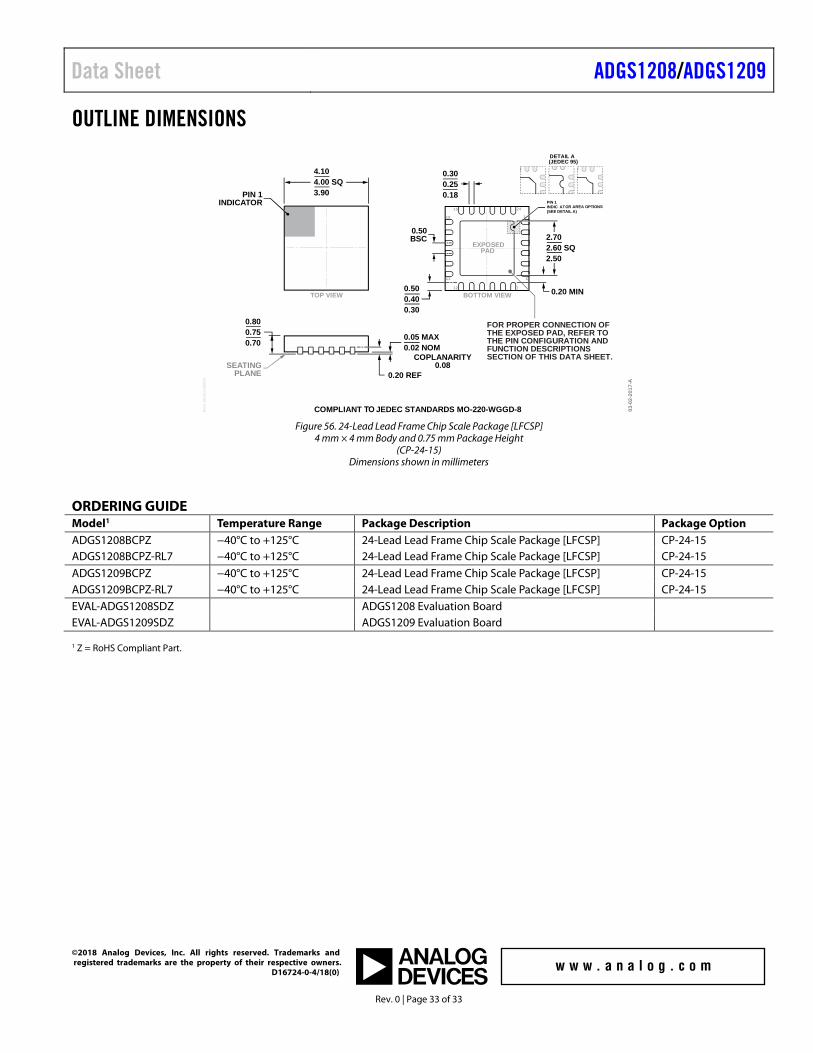
OUTLINE DIMENSIONS
0.800.750.70
PKG
-004
273/
5069
0.50BSC
0.500.400.30
COMPLIANT TO JEDEC STANDARDS MO-220-WGGD-8
BOTTOM VIEWTOP VIEW
4.104.00 SQ3.90
0.05 MAX0.02 NOM
0.20 REF
COPLANARITY0.08
PIN 1INDICATOR
1
24
712
13
18
19
6
03-0
2-20
17-A
0.300.250.18
0.20 MIN
2.702.60 SQ2.50
EXPOSEDPAD
SEATINGPLANE
PIN 1INDIC ATOR AREA OPTIONS(SEE DETAIL A)
DETAIL A(JEDEC 95)
FOR PROPER CONNECTION OFTHE EXPOSED PAD, REFER TOTHE PIN CONFIGURATION ANDFUNCTION DESCRIPTIONSSECTION OF THIS DATA SHEET.
Figure 56. 24-Lead Lead Frame Chip Scale Package [LFCSP]
4 mm × 4 mm Body and 0.75 mm Package Height (CP-24-15)
Dimensions shown in millimeters
ORDERING GUIDE Model1 Temperature Range Package Description Package Option ADGS1208BCPZ −40°C to +125°C 24-Lead Lead Frame Chip Scale Package [LFCSP] CP-24-15 ADGS1208BCPZ-RL7 −40°C to +125°C 24-Lead Lead Frame Chip Scale Package [LFCSP] CP-24-15 ADGS1209BCPZ −40°C to +125°C 24-Lead Lead Frame Chip Scale Package [LFCSP] CP-24-15 ADGS1209BCPZ-RL7 −40°C to +125°C 24-Lead Lead Frame Chip Scale Package [LFCSP] CP-24-15 EVAL-ADGS1208SDZ ADGS1208 Evaluation Board EVAL-ADGS1209SDZ ADGS1209 Evaluation Board 1 Z = RoHS Compliant Part.
©2018 Analog Devices, Inc. All rights reserved. Trademarks and registered trademarks are the property of their respective owners. D16724-0-4/18(0)