Embed Size (px)
Citation preview
LETTERSPUBLISHED ONLINE: 11 JULY 2016 | DOI: 10.1038/NMAT4685
Spectroscopic evidence for a type II Weylsemimetallic state in MoTe2
Lunan Huang1, Timothy M. McCormick2, Masayuki Ochi3, Zhiying Zhao4, Michi-To Suzuki5,Ryotaro Arita5,6, YunWu1, Daixiang Mou1, Huibo Cao7, Jiaqiang Yan8,9, Nandini Trivedi2
and Adam Kaminski1*In a type I Dirac or Weyl semimetal, the low-energy statesare squeezed to a single point in momentum space when thechemical potential µ is tuned precisely to the Dirac/Weylpoint1–6. Recently, a type II Weyl semimetal was predicted toexist, where the Weyl states connect hole and electron bands,separated by an indirect gap7–10. This leads to unusual energystates, where hole and electron pockets touch at the Weylpoint. Here we present the discovery of a type II topologicalWeyl semimetal state in pure MoTe2, where two sets of Weylpoints (W±
2 ,W±
3 ) exist at the touching points of electron andhole pockets and are located at dierent binding energiesabove EF. Using angle-resolved photoemission spectroscopy,modelling, density functional theory and calculations of Berrycurvature, we identify the Weyl points and demonstrate thatthey are connected by dierent sets of Fermi arcs for each ofthe two surface terminations. We also find new surface ‘trackstates’ that form closed loops and are unique to type II Weylsemimetals. This material provides an exciting, new platformto study the properties of Weyl fermions.
It is surprising and yet exhilarating that non-interactingor quadratic Hamiltonians can continue to provide so muchrichness from graphene, to topological insulators and topologicalsuperconductors. This list was recently expanded by the discoveryof topological Weyl semimetals (TWSs), the relatively robust three-dimensional analogues of graphene. With all three Pauli matricesinvolved in the Hamiltonian, perturbations only shift the positionof the node in momentum space but do not open a gap.
While the massless solution to the Dirac equation11 was firstproposed by Hermann Weyl in 1929, there are no known examplesof Weyl fermions in particle physics. Quantummaterials’ analogueshave been proposed in various classes of topological Dirac12–14 andWeyl semimetals where a pair of Dirac nodes can be separatedinto two Weyl points (WPs) by breaking either inversion or time-reversal invariance. The topological nature of a TWS is reflected inthe Berry fluxes of opposite chirality circulating around theWPs andthe presence of a Fermi arc formed between the projections of thetwo WPs on a surface at which the bulk is truncated.
Recently, two types of TWS have been identified: type I TWSscan be understood as the limiting point of a semiconductor witha direct bandgap that closes linearly at a set of isolated points.As a consequence, there is zero density of states if the chemical
potential is tuned to the energy of the WPs. Type I TWSs have beenpredicted and observed in the TaAs family (TaAs, NbAs and TaP)1–6,and also predicted to occur in pyrochlore iridates15 and carbonallotropes16. Type II TWSs, on the other hand, can be understoodas the limiting point of an indirect gap semiconductor that evolvesinto a compensated semimetal with electron and hole pockets thattouch at a set of isolated points with a finite density of states at thechemical potential17. The two WPs connected by a Fermi arc neednot occur at the same energy. MoTe2, WTe2 and SrSi2 are predictedto be such a type II TWS7–10. The calculations based on preciselydetermined lattice parameters point to the presence of a quadrupletof WPs and the presence of line nodes18. The line nodes are veryinteresting topological objects that form closed contours of one-dimensional Fermi surfaces in the momentum space19,20 that are yetto be observed experimentally. Strong spin–orbit coupling can, inprinciple, break them in to arcs, the presence of which was recentlyreported in extreme high magnetoresistive PtSn4 (ref. 21). Thereare some signatures of a type II TWS state in the mixed compoundMo0.45W0.55Te2 (ref. 22). Here we present the first evidence for sucha state in the stoichiometric, low-scattering material MoTe2.
One of the most exciting properties of a TWS is the existenceof gapless Fermi arcs on the surface. A Fermi surface, defined asthe locus of gapless excitations, is typically a closed contour thatseparates filled states from empty states at zero temperature. Inview of that, a chopped up Fermi surface with the two pieces onopposite surfaces is a novel state of matter. Surface-sensitive probessuch as angle-resolved photoemission spectroscopy have a decidedadvantage in investigating the structure of arcs, connectivity ofelectron and hole pockets and locations of WPs, which is the topicof our paper.
To set the stage for interpretation of the experimental results, weinvestigate a two-band latticemodel that breaks inversion symmetrybut is invariant under time-reversal symmetry. The main lessonslearnt by examining this model are shown in Fig. 1 and summarizedhere. First, the minimum number of four Weyl nodes in this type IITWS occur at E = 0 at the touching point of electron and holepockets in contrast with a type I TWS that has a zero density ofstates at E = 0. The touching of electron and hole bands in ourmodel is similar to the touching of the electron and hole bandsin the experimental data shown in Fig. 2a,b. Second, for a slabgeometry, constant-energy cuts at E=0 show Fermi arcs on surface
1Ames Laboratory, US DOE and Department of Physics and Astronomy, Iowa State University, Ames, Iowa 50011, USA. 2Department of Physics and Centerfor Emergent Materials, The Ohio State University, Columbus, Ohio 43210, USA. 3Department of Physics, Osaka University, Toyonaka, Osaka 560-0043,Japan. 4Department of Physics and Astronomy, University of Tennessee, Knoxville, Tennessee 37996, USA. 5RIKEN Center for Emergent Matter Science(CEMS), Wako, Saitama 351-0198, Japan. 6JST ERATO Isobe Degenerate π-Integration Project, Advanced Institute for Materials Research (AIMR), TohokuUniversity, Sendai, Miyagi 980-8577, Japan. 7Quantum Condensed Matter Division, Oak Ridge National Laboratory, Oak Ridge, Tennessee 37831, USA.8Materials Science and Technology Division, Oak Ridge National Laboratory, Oak Ridge, Tennessee 37831, USA. 9Department of Materials Science andEngineering, University of Tennessee, Knoxville, Tennessee 37996, USA. *e-mail: [email protected]
NATUREMATERIALS | ADVANCE ONLINE PUBLICATION | www.nature.com/naturematerials 1
© 2016 Macmillan Publishers Limited. All rights reserved
LETTERS NATUREMATERIALS DOI: 10.1038/NMAT4685
1 2 3
−4
−2
2
4
1 2 3−2 −1 −3 −2 −1 −3 −2 −11 2
−3
−2
2
3
−2
−5
0E/t
5
= −0.1tµ = 0.1tµ
−20
0
2
2
kx
kx kzkx
kz
kz kz
−2
−5
0E/t
5
−20
0
2
2
kx
kz
kz−1 1
−4
−2
2
4
d
eb c 11 22
Cut 1
Cut 2
a
E/t
E/t
−3 −2 2 3
3
2
1
−3 3
−1−1
−2
−3
1
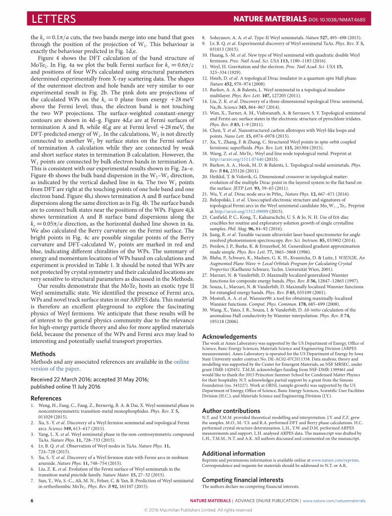
Figure 1 | A simple model of the type II Weyl semimetal described by a two-band model given by equation (2) that exhibits fourWeyl nodes. a, Electronicband structure for µ=±0.1t indicated by the blue translucent plane. b,c, The topological surface states and Fermi arcs on surface A (in red) and B (in blue)are calculated for a slab geometry confined along the y-direction. The bulk bands are shown in black. When µ=0 exactly, the electron and hole pocketstouch and the arcs terminate on the node (green dot) itself. For Fermi energy below (above) the nodal energy, arcs of surface states connect the Fermi hole(electron) pockets surrounding a node rather than terminating on a node. d,e, Energy dispersion along kz at fixed kx as shown by the cuts in b,c. Cut 1 alongkx=π/2 shows the bulk electron and hole bands touching at the node and the merging of surface states into the bulk away from the Weyl node. Cut 2along kx=0.63π shows a gap between the bulk bands and a surface state that disperses with opposite velocities at the projections of the two WPs. TheWPs are located at (kx,kz)= (±π/2,±π/2) indicated by pink arrows pointing to green dots.
termination A and B that connect WPs of opposite chirality. Inaddition there arewhat we term ‘track states’ that exist on the surfaceand pass through theWPs but, unlike Fermi arcs, form closed loops.For E < 0, the projections of the WPs are within the hole pocket,and at the surface the arc states connect the two hole pockets andthe track states loop around the electron pockets. The opposite istrue for E>0. Third, the energy dispersion clearly shows a surfacestate dispersing separately from the bulk bands and merging withthe bulk bands close to the WP in Fig. 1d. This is corroborated bythe experimental data around the Weyl nodes in Fig. 2i and Fig. 3owhere the arc merges with the bulk states.
We consider the following Hamiltonian for a two-band latticemodel that breaks inversion symmetry and is invariant under time-reversal:
HInv=∑k
c†kα(H(k))αβ ckβ (1)
where c(†)kα annihilates (creates) an electron atmomentum k in orbitalα and
H(k)=γ (cos(2kx)−cos(k0))(cos(kz)−cos(k0))σ0
− (m(1−cos2(kz)−cos(ky))+2tx(cos(kx)−cos(k0)))σ1
−2t sin(ky)σ2−2t cos(kz)σ3 (2)
Here σi is the ith Pauli matrix for i= 1, 2, 3 and σ0 is the 2× 2identity matrix. This model has four Weyl nodes located at E=0
and k = (±k0, 0,±π/2). The term in H(k) proportional to σ0produces a uniform shift in both energy bands. Such a momentum-dependent shift will result in a non-vanishing density of states fromelectron and hole pockets that touch at the Weyl node and a tiltof the Weyl nodes characteristic of a type II TWS. Henceforth, weset the parameters m= 2t , tx = t/2, k0= π/2, and γ = 2.4t . Thebulk band structure for this parameter choice can be seen in Fig. 1a,which shows hole and electron pockets touching at the Weyl nodesas well as pockets disconnected from the nodes. Similar Fermiologyis also present in the MoTe2 system and we can gain insight into thisand other relatedmaterials by taking advantage of the latticemodel’ssimplicity and tunability.
We examine the structure of the surface-state configuration byconsidering themodel in equation (1) in a slab geometry finite in they-direction with L layers but infinite in the x- and z-directions. Welabel the states as ‘surface termination B’ (‘surface termination A’) ifthey are exponentially localized at 〈y〉= 1 (〈y〉=L). Figure 1 alsoshows the surface states at µ=±0.1t overlaid on the bulk bandstructure.We show constant-energy cuts through the band structureof the slab geometry in Fig. 1b,c for µ=±0.1t . When µ< 0, theprojections of the Weyl nodes (shown by green dots) are enclosedby hole pockets. Each of these hole pockets is connected to anotherpocket containing a node of opposite chirality by one Fermi arc onsurface A (B) shown as a thick light red (blue) line. Whenµ>0, theprojections of the Weyl nodes are enclosed by electron pockets thatare similarly connected by Fermi arcs on the surfaces. At preciselyµ=0, because all of the nodes lie at E=0, all Fermi arcs terminateon the nodes themselves as in a type I TWS.
2
© 2016 Macmillan Publishers Limited. All rights reserved
NATUREMATERIALS | ADVANCE ONLINE PUBLICATION | www.nature.com/naturematerials
NATUREMATERIALS DOI: 10.1038/NMAT4685 LETTERS
−0.4
−0.2
0.0
0.2
0.4k y
(π/a
)k y
(π/a
)k y
(π/a
)
kx (π/b)
kx (π/b) kx (π/b)
k y (π
/a)
ky (π/a) ky (π/a)
a
W2 exp
W3 exp
W2 calc
FS, 6.7 eV
bFS + 10 meV
−0.4
−0.2
0.0
0.2
0.4
−0.4 −0.2 0.0 0.2
cHole band (HB) 1Weyl pointsHB 2EB 1
Fermi arcs
EB 2Arc W2−W3Arc W2−W2
−100
−80
−60
−40
−20
0
20
40 kx = 0.32(π/b)g
−100
−80
−60
−40
−20
0
20
40
E − E f
(meV
)E
− E f
(meV
)E
− E f
(meV
)E
− E f
(meV
)
kx = 0.36(π/b)f
W3 exp
−100
−80
−60
−40
−20
0
20
40 kx = 0.28(π/b)h
−0.2 0.0 0.2−100
−80
−60
−40
−20
0
20
40 kx = 0.24(π/b)i
k
j
l
mW2 exp
0.4
0.2
0.0
−0.2−0.4 −0.2 0.0
FS + 30 meVd e
−0.4 −0.2 0.0
FS − 30 meV
kx = 0.36(π/b)
kx = 0.32(π/b)
kx = 0.28(π/b)
−0.2 0.0 0.2
kx = 0.24(π/b)
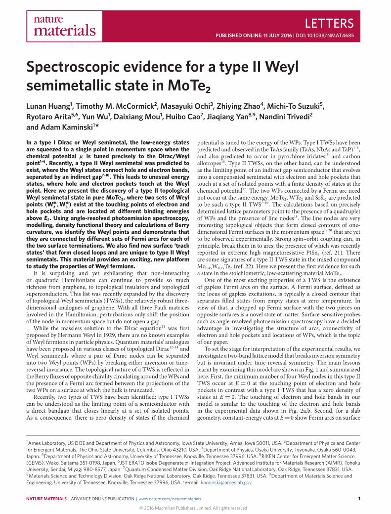
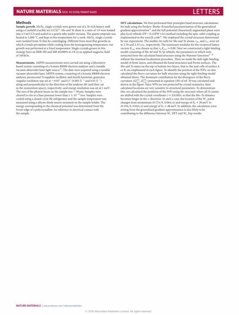
Figure 2 | Experimental Fermi surface and band structure of MoTe2. a, Constant-energy intensity plot measured at EF using 6.7 eV photons for a samplewith termination A. The calculated (DFT) positions of WPs W2 are marked as pink dots, while experimentally determined locations of W2 and W3 pointsare marked as red dots. The chiralities of WPs are marked with ‘+’ and ‘−’ and their locations (kx,ky ,E) are summarized in Table 1. b, Same plot as in abut taken at 10 meV above EF. c, A sketch of constant-energy contours of electron and hole bands showing the locations of WPs and Fermi arcs.d, Constant-energy contour measured at 30 meV above EF using 5.9 eV photons for a sample with termination B. Positions of calculated and measuredWPs are marked as above. e, Same surface termination and photon energy as in d but at 30 meV below EF. f–i, Experimental band dispersion along cuts atkx=0.24, 0.28, 0.32 and 0.36 π/b. White dashed lines mark locations of the electron bands and red dashed lines mark the locations of the hole bands.j–m, Calculated band dispersion for a sample with termination A along kx=0.24, 0.28, 0.32 and 0.36 π/b. Bands plotted with darker lines have moresurface weights. Dashed black lines in a–d connect the Γ point to symmetry points and to corners of the Brillouin zone.
The slab configuration energy dispersion for fixed kx is shown inFig. 1d,e. These cuts are shown as green dashed lines labelled cut 1and cut 2 respectively. We can see that at the Weyl nodes, the redsurface bands in Fig. 1d disappear into the bulk. As we move pastthe WPs in Fig. 1e, we see that these two red bands combine into asingle continuous band.
MoTe2 crystallizes in an orthorhombic lattice. Of the threedifferent polymorphs, only the Td phase (space group Pmn21,No. 31) lacks inversion symmetry and can therefore host the Weylstate7. Details of crystal growth and angle-resolved photoemissionspectroscopy (ARPES)measurements are discussed in theMethods.
The Fermi surface of MoTe2 also has two 2-fold symmetryaxes, along Γ –X and Γ –Y directions. The lattice constants area=6.33Å, b=3.469Å.
We identify electron and hole bands in the spectroscopic datashown in Figs 2 and 3. The hole bands at the centre of the Brillouinzone have a ‘butterfly’ shape. The electron pockets shaped like ovalsare located on each side of the butterfly. There are also two banana-like hole pockets partially overlapping the oval electron pockets. Theconfiguration of these pockets can be seen at the Fermi energy inFig. 2a and 10meV above the Fermi energy in Fig. 2b and theirelectron or hole character is easily identified because hole (electron)
NATUREMATERIALS | ADVANCE ONLINE PUBLICATION | www.nature.com/naturematerials
© 2016 Macmillan Publishers Limited. All rights reserved
3
LETTERS NATUREMATERIALS DOI: 10.1038/NMAT4685
−0.1
0.0
−0.6
−0.5
−0.4
−0.3
−0.2
−0.1
0.06.7 eV, FS, bottom
W2 exp
W3 exp
W2 calc
b
0.250.10−0.1
0.0
0.250.10 0.250.100.250.10
−0.4 −0.2 0.0 0.2 0.4
−0.4
−0.3
−0.2
−0.1
0.0
0.1
0.25.9 eV, FS, bottom
W2 exp
W3 exp
W2 calc
c
−0.1
0.0
ky = 0(π/a) ky = 0.05(π/a) ky = 0.1(π/a) ky = 0.2(π/a)
MoTe
−0.6
−0.5
−0.4
−0.3
−0.2
−0.1
0.06.7 eV, FS, top
W2 calc
Cut e f g h
W2 exp
W2 exp
a
W2 calc
−0.1
0.0
0.1
Band 1
Band 2
Band 3
0.250.10−0.1
0.0
0.1
0.250.10
Band 1Band 2
Band 3
0.250.10
W2 calc
0.250.10
d
e f g h
i j k l
m n o p
q r s t
u v w x
“B”
“A”
“B”
“A”
k x (π
/b)
k x (π
/b)
k x (π
/b)
kx (π/b) kx (π/b) kx (π/b) kx (π/b)
kx (π/b) kx (π/b) kx (π/b) kx (π/b)
ky (π/a)
W2 exp
W2 exp
W2 exp
E − E f
(eV
)E
− E f
(eV
)E
− E f
(eV
)E
− E f
(eV
)E
− E f
(eV
)
a
c
b
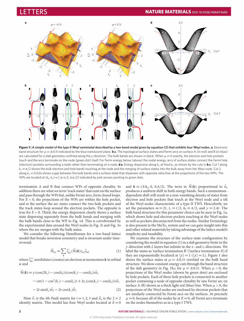
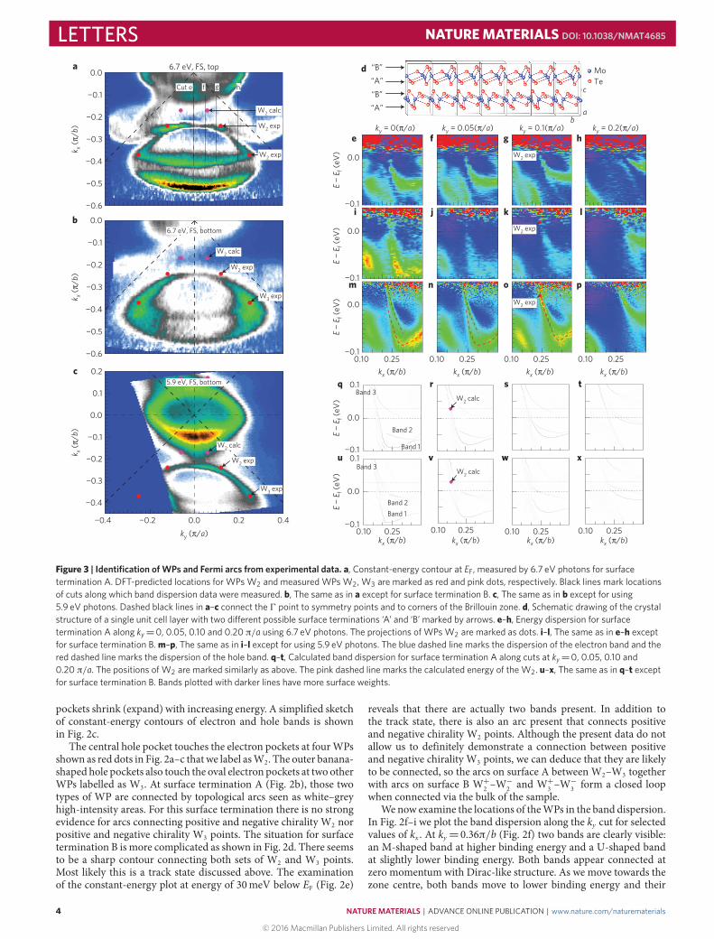
Figure 3 | Identification of WPs and Fermi arcs from experimental data. a, Constant-energy contour at EF, measured by 6.7 eV photons for surfacetermination A. DFT-predicted locations for WPs W2 and measured WPs W2, W3 are marked as red and pink dots, respectively. Black lines mark locationsof cuts along which band dispersion data were measured. b, The same as in a except for surface termination B. c, The same as in b except for using5.9 eV photons. Dashed black lines in a–c connect the 0 point to symmetry points and to corners of the Brillouin zone. d, Schematic drawing of the crystalstructure of a single unit cell layer with two dierent possible surface terminations ‘A’ and ‘B’ marked by arrows. e–h, Energy dispersion for surfacetermination A along ky=0, 0.05, 0.10 and 0.20 π/a using 6.7 eV photons. The projections of WPs W2 are marked as dots. i–l, The same as in e–h exceptfor surface termination B. m–p, The same as in i–l except for using 5.9 eV photons. The blue dashed line marks the dispersion of the electron band and thered dashed line marks the dispersion of the hole band. q–t, Calculated band dispersion for surface termination A along cuts at ky=0, 0.05, 0.10 and0.20 π/a. The positions of W2 are marked similarly as above. The pink dashed line marks the calculated energy of the W2. u–x, The same as in q–t exceptfor surface termination B. Bands plotted with darker lines have more surface weights.
pockets shrink (expand) with increasing energy. A simplified sketchof constant-energy contours of electron and hole bands is shownin Fig. 2c.
The central hole pocket touches the electron pockets at fourWPsshown as red dots in Fig. 2a–c that we label asW2. The outer banana-shaped hole pockets also touch the oval electron pockets at two otherWPs labelled as W3. At surface termination A (Fig. 2b), those twotypes of WP are connected by topological arcs seen as white–greyhigh-intensity areas. For this surface termination there is no strongevidence for arcs connecting positive and negative chirality W2 norpositive and negative chirality W3 points. The situation for surfacetermination B is more complicated as shown in Fig. 2d. There seemsto be a sharp contour connecting both sets of W2 and W3 points.Most likely this is a track state discussed above. The examinationof the constant-energy plot at energy of 30meV below EF (Fig. 2e)
reveals that there are actually two bands present. In addition tothe track state, there is also an arc present that connects positiveand negative chirality W2 points. Although the present data do notallow us to definitely demonstrate a connection between positiveand negative chirality W3 points, we can deduce that they are likelyto be connected, so the arcs on surface A between W2–W3 togetherwith arcs on surface B W+2 –W
−
2 and W+3 –W−
3 form a closed loopwhen connected via the bulk of the sample.
We now examine the locations of theWPs in the band dispersion.In Fig. 2f–i we plot the band dispersion along the ky cut for selectedvalues of kx . At ky=0.36π/b (Fig. 2f) two bands are clearly visible:an M-shaped band at higher binding energy and a U-shaped bandat slightly lower binding energy. Both bands appear connected atzero momentum with Dirac-like structure. As we move towards thezone centre, both bands move to lower binding energy and their
4
© 2016 Macmillan Publishers Limited. All rights reserved
NATUREMATERIALS | ADVANCE ONLINE PUBLICATION | www.nature.com/naturematerials
NATUREMATERIALS DOI: 10.1038/NMAT4685 LETTERSTable 1 |The locations (kx,ky,E) of theWPs fromDFT(calculatedusing experimental crystal structure parameters) and ARPES.
kx (π/b) ky (π/a) E (meV)
W2 DFT ±0.17 ±0.06 28W2 Exp ±0.24 ±0.12 20W3 Exp ±0.37 ±0.25 30
energy separation decreases. In Fig. 2h, the tips of the M-shapedband (red dotted line) touch the EF and form parts of the butterflyhole pockets. As these tipsmove aboveEF, theymergewith thewingsof the U-shaped electron band (white dotted line) forming twoWPsapproximately 20meV above EF marked by black dots. At each sideof the symmetry line, they form two tilted cones characteristic of atype II Weyl node. The MoTe2 samples cleave between two adjacentTe layers (see Fig. 3d). The crystal structure of the Td phase, whichhosts the Weyl state, breaks the inversion symmetry and there aretwo MoTe2 layers per unit cell. This gives rise to two chemicallysimilar, but structurally different cleaving planes ‘A’ and ‘B’, as shownin Fig. 3d. The electronic structure of each termination is expected tobe slightly different due to the different length of the Mo–Te bonds.The data along the kx direction are shown in Fig. 3e–p along withresults of calculations (Fig. 3q–x) for the two surface terminations.
The surface termination A is characterized by lower binding energyof the electron pocket in Fig. 3e–h, when compared with thedata from surface termination B shown in Fig. 3i–p. The data inFig. 3m–p best illustrate the formation of theW2 points. In Fig. 3m,the hole band is marked with a red dashed line, while the electronband is marked with a blue dashed line. As we move away from thesymmetry line, the separation between those bands becomes smallerand they merge at a point located∼20meV above EF marked by ared dot in panel Fig. 3o. For higher values of ky momentum theyseparate again as seen in panel Fig. 3p. The density functional theory(DFT) calculation also demonstrates the energy difference of theband locations for the two terminations and formation of the W2WP that agrees with experiment on a qualitative level. The details ofthe DFT calculations are provided in the Methods.
The momentum location of the experimentally determinedWPsis different fromDFTpredictions (marked as pink dots in 2a,b)mostlikely due to high sensitivity of the band calculation to structuralparameters. Table 1 summarizes the positions of WPs determinedfrom experiment and DFT. Despite the discrepancy between thepredicted locations of the Weyl nodes from DFT and where theyare located experimentally, in each case they are at the touchingpoints of the electron and hole bands. In the ky= 0 cuts shown inFig. 3e,l,m,q,u, band 1 is connected to bulk states below the Fermilevel, while band 3dips down and goes into bulk just before it reachesthe WP. As we increase ky , band 1 and band 3merge together. In
0.6
0.5
0.4
0.3
0.2
0.1
Termination A, FSd
0.6
0.5
0.4
0.3
0.2
0.1−0.4 −0.2 0.0 0.2 0.4
Termination B, FSe
A, FS + 28 meVf
−0.4 −0.2 0.0 0.2 0.4
B, FS + 28 meVg
A, ky = 0.05(π/a)
j
0.60.50.40.30.20.10.0
B, ky = 0.05(π/a)
W2 energy level = 28 meVW2 calc projection
k
−0.20
−0.15
−0.10
−0.05
0.00
0.05
0.10
−0.3 −0.2 −0.1 0.0 0.1 0.2 0.3
Bulk band dispersion at W2−W2b
−0.2
−0.1
0.0
0.1
A, W2−W2 cut
h
−0.2
−0.1
0.0
0.1
−0.1 0.0 0.1
B, W2−W2 cut
i
c Berry curvature
ky (π/a)
ky (π/a) ky (π/a) ky (π/a) ky (π/a)
ky (π/a)
−0.4
−0.2
0.0
0.2
0.4
−0.4 −0.2 0.0 0.2 0.4
Bulk Fermi surface
W2 calc (0.17, 0.06)
a
k y (π
/a)
kx (π/b)
k x (π
/b)
k x (π
/b)
0
0.2
0.4
0.6
−0.4 −0.2 0 0.2 0.40
500
1,000
1,500
k x (π
/b)
E − E f
(eV
)
E − E f
(eV
)
E − E f
(eV
)
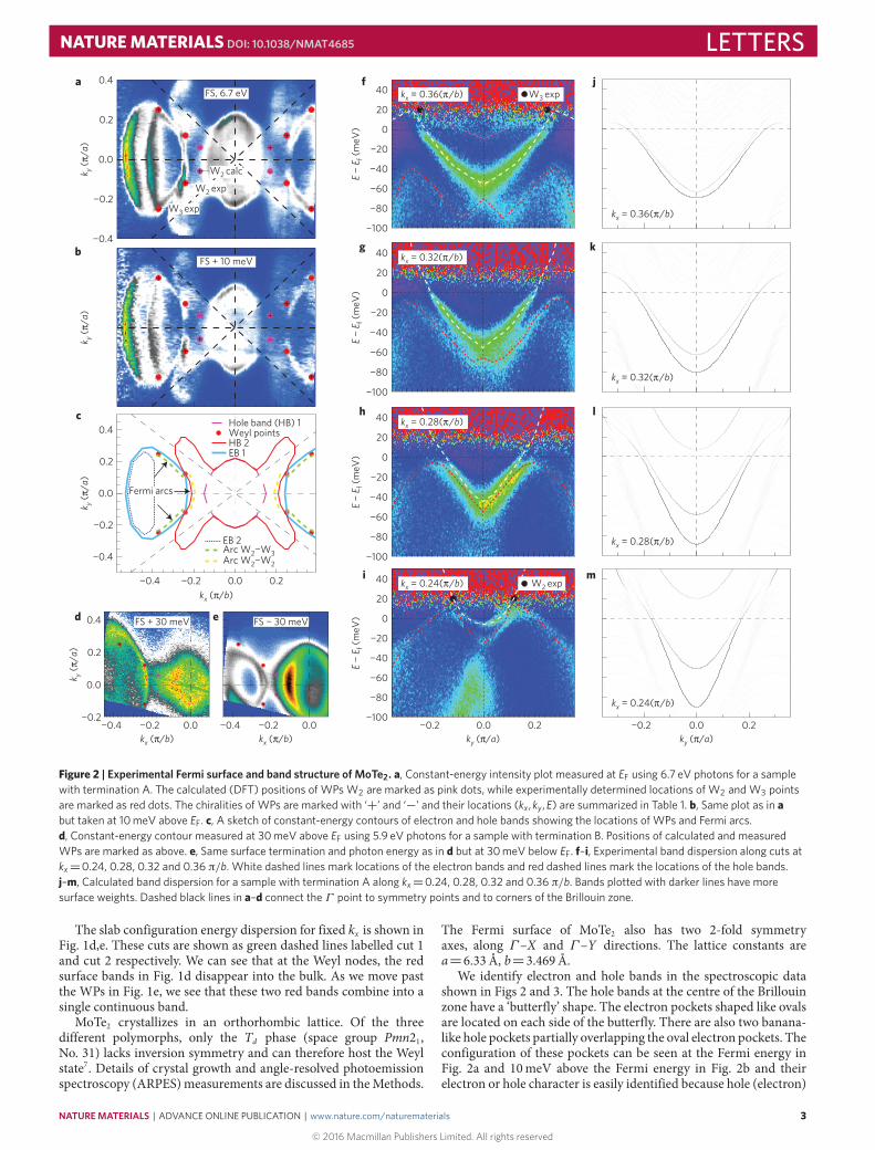
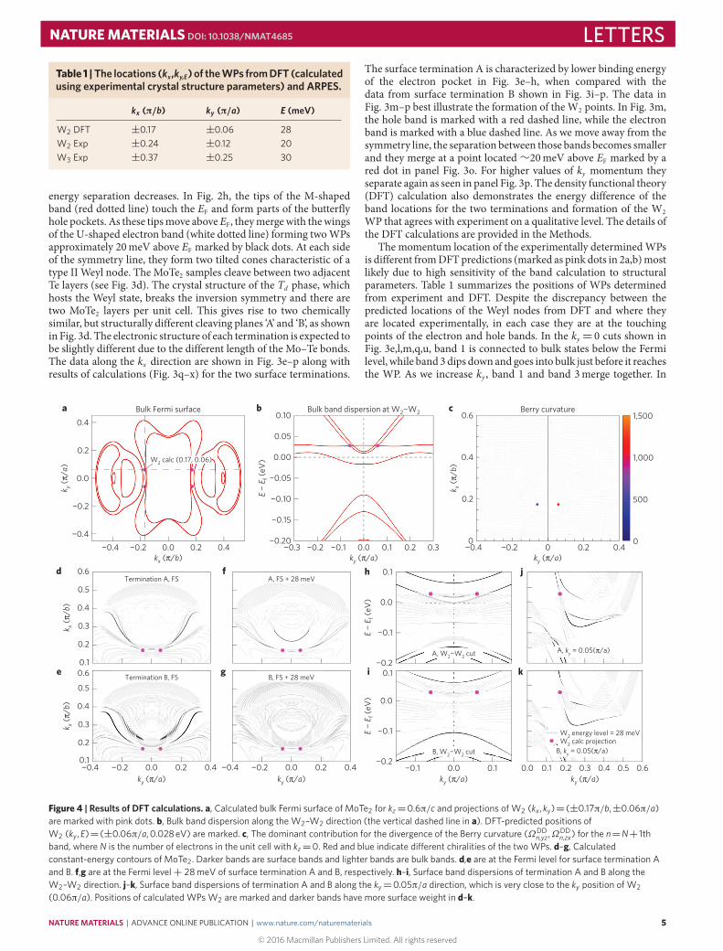
Figure 4 | Results of DFT calculations. a, Calculated bulk Fermi surface of MoTe2 for kz=0.6π/c and projections of W2 (kx,ky)= (±0.17π/b,±0.06π/a)are marked with pink dots. b, Bulk band dispersion along the W2–W2 direction (the vertical dashed line in a). DFT-predicted positions ofW2 (ky ,E)= (±0.06π/a, 0.028 eV) are marked. c, The dominant contribution for the divergence of the Berry curvature (ΩDD
n,yz,ΩDDn,zx) for the n=N+ 1th
band, where N is the number of electrons in the unit cell with kz=0. Red and blue indicate dierent chiralities of the two WPs. d–g, Calculatedconstant-energy contours of MoTe2. Darker bands are surface bands and lighter bands are bulk bands. d,e are at the Fermi level for surface termination Aand B. f,g are at the Fermi level+ 28 meV of surface termination A and B, respectively. h–i, Surface band dispersions of termination A and B along theW2–W2 direction. j–k, Surface band dispersions of termination A and B along the ky=0.05π/a direction, which is very close to the ky position of W2(0.06π/a). Positions of calculated WPs W2 are marked and darker bands have more surface weight in d–k.
NATUREMATERIALS | ADVANCE ONLINE PUBLICATION | www.nature.com/naturematerials
© 2016 Macmillan Publishers Limited. All rights reserved
5
LETTERS NATUREMATERIALS DOI: 10.1038/NMAT4685
the ky=0.1π/a cuts, the two bands merge into one band that goesthrough the position of the projection of W2. This behaviour isexactly the behaviour predicted in Fig. 1d,e.
Figure 4 shows the DFT calculation of the band structure ofMoTe2. In Fig. 4a we plot the bulk Fermi surface for kz = 0.6π/cand positions of four WPs calculated using structural parametersdetermined experimentally from X-ray scattering data. The shapesof the outermost electron and hole bands are very similar to ourexperimental result in Fig. 2b. The pink dots are projections ofthe calculated WPs on the kz = 0 plane from energy +28meVabove the Fermi level; thus, the electron band is not touchingthe two WP projections. The surface-weighted constant-energycontours are shown in 4d–g. Figure 4d,e are at Fermi surfaces oftermination A and B, while 4f,g are at Fermi level +28meV, theDFT-predicted energy of W2. In the calculations, W2 is not directlyconnected to another W2 by surface states on the Fermi surfaceof termination A calculation while they are connected by weakand short surface states in termination B calculation. However, theW2 points are connected by bulk electron bands in termination A.This is consistent with our experimental results shown in Fig. 2a–e.Figure 4b shows the bulk band dispersion in the W2–W2 direction,as indicated by the vertical dashed line in 4a. The two W2 pointsfrom DFT are right at the touching points of one hole band and oneelectron band. Figure 4h,i shows termination A and B surface banddispersions along the same direction as in Fig. 4b. The surface bandsare to connect bulk states near the positions of the WPs. Figure 4j,kshows termination A and B surface band dispersions along theky= 0.05π/a direction, as the horizontal dashed line shown in 4a.We also calculated the Berry curvature on the Fermi surface. Thebright points in Fig. 4c are possible singular points of the Berrycurvature and DFT-calculated W2 points are marked in red andblue, indicating different chiralities of the WPs. The summary ofenergy and momentum locations of WPs based on calculations andexperiment is provided in Table 1. It should be noted that WPs arenot protected by crystal symmetry and their calculated locations arevery sensitive to structural parameters as discussed in the Methods.
Our results demonstrate that the MoTe2 hosts an exotic type IIWeyl semimetallic state. We identified the presence of Fermi arcs,WPs and novel track surface states in our ARPES data. Thismaterialis therefore an excellent playground to explore the fascinatingphysics of Weyl fermions. We anticipate that these results will beof interest to the general physics community due to the relevancefor high-energy particle theory and also for more applied materialsfield, because the presence of the WPs and Fermi arcs may lead tointeresting and potentially useful transport properties.
MethodsMethods and any associated references are available in the onlineversion of the paper.
Received 22 March 2016; accepted 31 May 2016;published online 11 July 2016
References1. Weng, H., Fang, C., Fang, Z., Bernevig, B. A. & Dai, X. Weyl semimetal phase in
noncentrosymmetric transition-metal monophosphides. Phys. Rev. X 5,011029 (2015).
2. Xu, S.-Y. et al . Discovery of a Weyl fermion semimetal and topological Fermiarcs. Science 349, 613–617 (2015).
3. Yang, L. X. et al . Weyl semimetal phase in the non-centrosymmetric compoundTaAs. Nature Phys. 11, 728–733 (2015).
4. Lv, B. Q. et al . Observation of Weyl nodes in TaAs. Nature Phys. 11,724–728 (2015).
5. Xu, S.-Y. et al . Discovery of a Weyl fermion state with Fermi arcs in niobiumarsenide. Nature Phys. 11, 748–754 (2015).
6. Liu, Z. K. et al . Evolution of the Fermi surface of Weyl semimetals in thetransition metal pnictide family. Nature Mater. 15, 27–32 (2015).
7. Sun, Y., Wu, S.-C., Ali, M. N., Felser, C. & Yan, B. Prediction of Weyl semimetalin orthorhombic MoTe2. Phys. Rev. B 92, 161107 (2015).
8. Soluyanov, A. A. et al . Type-II Weyl semimetals. Nature 527, 495–498 (2015).9. Lv, B. Q. et al . Experimental discovery of Weyl semimetal TaAs. Phys. Rev. X 5,
031013 (2015).10. Huang, S.-M. et al . New type of Weyl semimetal with quadratic double Weyl
fermions. Proc. Natl Acad. Sci. USA 113, 1180–1185 (2016).11. Weyl, H. Gravitation and the electron. Proc. Natl Acad. Sci. USA 15,
323–334 (1929).12. Hsieh, D. et al . A topological Dirac insulator in a quantum spin Hall phase.
Nature 452, 970–974 (2008).13. Burkov, A. A. & Balents, L. Weyl semimetal in a topological insulator
multilayer. Phys. Rev. Lett. 107, 127205 (2011).14. Liu, Z. K. et al . Discovery of a three-dimensional topological Dirac semimetal,
Na3Bi. Science 343, 864–867 (2014).15. Wan, X., Turner, A. M., Vishwanath, A. & Savrasov, S. Y. Topological semimetal
and Fermi-arc surface states in the electronic structure of pyrochlore iridates.Phys. Rev. B 83, 1–9 (2011).
16. Chen, Y. et al . Nanostructured carbon allotropes with Weyl-like loops andpoints. Nano Lett. 15, 6974–6978 (2015).
17. Xu, Y., Zhang, F. & Zhang, C. Structured Weyl points in spin-orbit coupledfermionic superfluids. Phys. Rev. Lett. 115, 265304 (2015).
18. Wang, Z. et al . MoTe2: Weyl and line node topological metal. Preprint athttp://arxiv.org/1511.07440 (2015).
19. Burkov, A. A., Hook, M. D. & Balents, L. Topological nodal semimetals. Phys.Rev. B 84, 235126 (2011).
20. Heikkil, T. & Volovik, G. Dimensional crossover in topological matter:evolution of the multiple Dirac point in the layered system to the flat band onthe surface. JETP Lett. 93, 59–65 (2011).
21. Wu, Y. et al . Dirac node arcs in PtSn4. Nature Phys. 12, 667–671 (2016).22. Belopolski, I. et al . Unoccupied electronic structure and signatures of
topological Fermi arcs in the Weyl semimetal candidate MoxW1−xTe2. Preprintat http://arxiv.org/1512.09099 (2015).
23. Canfield, P. C., Kong, T., Kaluarachchi, U. S. & Jo, N. H. Use of frit-disccrucibles for routine and exploratory solution growth of single crystallinesamples. Phil. Mag. 96, 84–92 (2016).
24. Jiang, R. et al . Tunable vacuum ultraviolet laser based spectrometer for angleresolved photoemission spectroscopy. Rev. Sci. Instrum. 85, 033902 (2014).
25. Perdew, J. P., Burke, K. & Ernzerhof, M. Generalized gradient approximationmade simple. Phys. Rev. Lett. 77, 3865–3868 (1996).
26. Blaha, P., Schwarz, K., Madsen, G. K. H., Kvasnicka, D. & Luitz, J.WIEN2K, AnAugmented Plane Wave+ Local Orbitals Program for Calculating CrystalProperties (Karlheinz Schwarz, Techn. Universität Wien, 2001).
27. Marzari, N. & Vanderbilt, D. Maximally localized generalized Wannierfunctions for composite energy bands. Phys. Rev. B 56, 12847–12865 (1997).
28. Souza, I., Marzari, N. & Vanderbilt, D. Maximally localized Wannier functionsfor entangled energy bands. Phys. Rev. B 65, 035109 (2001).
29. Mostofi, A. A. et al . Wannier90: a tool for obtaining maximally-localizedWannier functions. Comput. Phys. Commun. 178, 685–699 (2008).
30. Wang, X., Yates, J. R., Souza, I. & Vanderbilt, D. Ab initio calculation of theanomalous Hall conductivity by Wannier interpolation. Phys. Rev. B 74,195118 (2006).
AcknowledgementsThe work at Ames Laboratory was supported by the US Department of Energy, Office ofScience, Basic Energy Sciences, Materials Science and Engineering Division (ARPESmeasurements). Ames Laboratory is operated for the US Department of Energy by IowaState University under contract No. DE-AC02-07CH11358. Data analysis, theory andmodelling was supported by the Center for Emergent Materials, an NSF MRSEC, undergrant DMR-1420451. T.M.M. acknowledges funding from NSF-DMR-1309461 andwould like to thank the 2015 Princeton Summer School for Condensed Matter Physicsfor their hospitality. N.T. acknowledges partial support by a grant from the SimonsFoundation (no. 343227). Work at ORNL (sample growth) was supported by the USDepartment of Energy, Office of Science, Basic Energy Sciences, Scientific User FacilitiesDivision (H.C.), and Materials Science and Engineering Division (J.Y.).
Author contributionsN.T. and T.M.M. provided theoretical modelling and interpretation. J.Y. and Z.Z. grewthe samples. M.O., M.-T.S. and R.A. performed DFT and Berry phase calculations. H.C.performed crystal structure determination. L.H., Y.W. and D.M. performed ARPESmeasurements and support. L.H. analysed ARPES data. The manuscript was drafted byL.H., T.M.M., N.T. and A.K. All authors discussed and commented on the manuscript.
Additional informationReprints and permissions information is available online at www.nature.com/reprints.Correspondence and requests for materials should be addressed to N.T. or A.K.
Competing financial interestsThe authors declare no competing financial interests.
6
© 2016 Macmillan Publishers Limited. All rights reserved
NATUREMATERIALS | ADVANCE ONLINE PUBLICATION | www.nature.com/naturematerials
NATUREMATERIALS DOI: 10.1038/NMAT4685 LETTERSMethodsSample growth.MoTe2 single crystals were grown out of a Te-rich binary meltusing a Canfield crucible set (CCS)23. Mo and Te shots in a ratio of 1:9 were loadedinto a 5ml CCS and sealed in a quartz tube under vacuum. The quartz ampoule washeated to 1,000 C and kept at this temperature for a week. MoTe2 single crystalswere isolated from Te flux by centrifuging. Different from most flux growths inwhich crystals precipitate while cooling from the homogenizing temperature, ourgrowth was performed at a fixed temperature. Single crystals grown in thisstrategy have an RRR 500 and MR 40,000% at 2K in an applied magnetic fieldof 100 kOe.
Measurements. ARPES measurements were carried out using a laboratory-based system consisting of a Scienta R8000 electron analyser and a tunablevacuum ultraviolet laser light source24. The data were acquired using a tunablevacuum ultraviolet laser ARPES system, consisting of a Scienta R8000 electronanalyser, picosecond Ti:sapphire oscillator and fourth harmonic generator.Angular resolution was set at∼0.05 and 0.5 (0.005Å−1 and 0.05Å−1)along and perpendicular to the direction of the analyser slit (and thus cutin the momentum space), respectively; and energy resolution was set at 1meV.The size of the photon beam on the sample was∼30 µm. Samples werecleaved in situ at a base pressure lower than 1×10⁻¹⁰ torr. Samples werecooled using a closed-cycle He refrigerator and the sample temperature wasmeasured using a silicon-diode sensor mounted on the sample holder. Theenergy corresponding to the chemical potential was determined from theFermi edge of a polycrystalline Au reference in electrical contact withthe sample.
DFT calculations.We first performed first-principles band structure calculationsfor bulk using the Perdew–Burke–Ernzerhof parametrization of the generalizedgradient approximation25 and the full-potential (linearized) augmented plane waveplus local orbitals (FP−(L)APW+lo) method including the spin–orbit coupling asimplemented in the wien2k code26. We employed the crystal structure determinedby our experiment. The muffin-tin radii for Mo and Te atoms, rMo and rTe, were setto 2.50 and 2.33 a.u., respectively. The maximum modulus for the reciprocal latticevectors Kmax was chosen so that rTeKmax=8.00. Next we constructed a tight-bindingmodel consisting of Mo 4d and Te 5p orbitals, the parameters in which wereextracted from the calculated band structure using the Wannier functions27–29without the maximal localization procedure. Then we made the slab tight-bindingmodel of finite layers, and obtained the band structures and Fermi surfaces. TheMo and Te states on the top or bottom two layers, that is, the unit cells of surface Aor B, are emphasized in each figure. To identify the position of the WPs, we alsocalculated the Berry curvature for bulk structure using the tight-binding modelobtained above. The dominant contribution for the divergence of the Berrycurvature (ΩDD
n,yz ,ΩDDn,zx) presented in equation (30) of ref. 30 was calculated and
shown in the figure. Since WPs are not protected by crystal symmetry, theircalculated locations are very sensitive to structural parameters. To demonstratethis, we calculated the positions of the WPs using the structure where all Te atomsare shifted with the crystal coordinate z=±0.005c so that the Mo–Te distancebecomes longer in the z-direction. In such a case, the location of the W2 pointchanges from momentum (0.17π/b, 0.06π/a) and energy of EF+28meV to(0.19π/b, 0.04π/a) and energy of EF+48meV. In addition, the calculation errorarising from the generalized gradient approximation is also likely to becontributing to the difference between W2 DFT and W2 Exp results.
NATUREMATERIALS | www.nature.com/naturematerials
© 2016 Macmillan Publishers Limited. All rights reserved


![Electronic and transport properties of kinked graphene · outstanding electronic transport properties of graphene [1]. However, it is crucial to modify the semimetallic electronic](https://img.pdfslide.us/doc/110x75/5fd887529019ff628275f4c6/electronic-and-transport-properties-of-kinked-graphene-outstanding-electronic-transport.jpg)