Embed Size (px)
Citation preview

SPE-11-8-061/G | page 1 of 21
PA.25a
Specification
Part No. PA.25a
Product Name AnamHexa-Band Cellular SMD AntennaGSM / CDMA / DCS / PCS / WCDMA /UMTS /HSDPA / GPRS / EDGE 800 MHz to 2200 MHz
Feature High Efficiency Multi-Band SMD Antenna35*5*6mmRoHS Compliant
Anam

SPE-11-8-061/G | page 2 of 21
This ceramic multiband cellular antenna uses high grade ceramics which have been developed in Taoglas through years of expertise in delivering the right materials for high performance antennas.
Taoglas designers, through constant research and development have been able to “fit” 6 bands in a small area, while also achieving high efficiency. The PA.25 is a unique SMT solution which is delivered on
tape and reel. For very detailed integration information additional to this specification please download our comprehensive PA.25 integration application note from our website.
1. Highest efficiency in small size 35*5*6mm. A comparative metal, FR4, FPC, whip, rod, helix antenna would have much more reduced efficiency in this configuration for the same size due to their different dielectric constants.
2. More resistant to detuning compared to other antenna integrations. If tuning is required it can be tuned for the device environment. There is no need for new tooling, thereby saving money if customisation is required.
3. Highly reliable and robust– its predecessor the PA.22 antenna is used by the world’s leading auto makers in extremely challenging environments. The antenna meets all temperature and mechanical specs required (vibration, drop tests etc)
4. Rectangular shape - Easy to integrate. Other antenna designs come in irregular shapes and sizes making them hard to integrate.
5. SMD (On-Board) antenna saves on labor, cable and connector costs, leads to higher integration yield rates, and reduces losses in transmission.
6. It can be mounted directly on edge of device main-board.
7. Transmission losses are kept to absolute minimum resulting in much improved over the air (OTA) device performance compared to similar efficiency cable and connector antenna solutions
8. Reductions in probability of radiated spurious emissions compared to other antenna technologies are observed when using the PA.25 and strictly following this application note layout
9. Achieves moderate to high gain in both vertical and horizontal polarization planes.
This feature is very useful in certain wireless communications where the antenna orientation is not fixed and the reflections or multipath signals may be present from any plane. In those cases the important parameter to be considered is the total field strength, which is the vector sum of the signal from the horizontal and vertical polarization planes at any instant in time.
1. Introduction
1.1 Key Advantages

SPE-11-8-061/G | page 3 of 21
2. Electrical Characteristics
3. Key Antenna Performance Indicators
Parameter Specification
Working Frequency 824~960MHz to 1700~2170MHzDimensions 35*5*6mm
VSWR 3:1 max (depends on the special environment)
Polarization Linear
Impedance 50 Ω
Operating Temperature -40°C~+105°CTermination Ag (Environmentally Friendly Pb Free)
* Ground Plane Size 40*97mm* Actual Electrical value will depend on customer ground plane size.
Measured in Satimo Starlab system
Hexa-band Antenna PA.25a peak gain parameter Summary
Band GSM (MHz) 3G DCS (MHz) PCS (MHz) WCDMA (MHz)824 890 880 960 1700 1710 1880 1850 1990 2110 2170
Peak Gain (dBi) 1.49 0.92 1.76 1.35 2.40 2.53 2.38 2.30 2.46 2.69 4.62
Efficiency (%) 60.6 65.4 69.3 64.6 51.0 54.7 63.1 61.6 51.5 56.2 65.8
*Efficiency & Gain (Ground Plane Length: 97 mm)

SPE-11-8-061/G | page 4 of 21
3.1 Reference efficiency data with different ground plane length
3.2 S11 - Return Loss
Tr1 S11 Log Mag 3.000dB/ Ref 0.000dB [F1]
3.000
0.000
-3.000
-6.000
-9.000
-12.00
-15.00
-18.00
-21.00
-24.00
-27.00
11
4
>1 824.00000 MHz -6.3905 dB>2 960.00000 MHz -12.714 dB>3 1.7100000 GHz -10.787 dB>4 2.1700000 GHz -13.510 dB
3
2

SPE-11-8-061/G | page 5 of 21
3.3 S11 – Smith Chart
Tr1 S11 Smith (R+j X) Scale 1.000U [F1]
1 824.00000 MHz 32.824 Ω -41.861 Ω 4.6141 pF2 960.00000 MHz 51.214 Ω 29.208 Ω 4.8422 nH3 1.7100000 GHz 31.210 Ω 8.0208 Ω 746.52 pH
>4 2.1700000 GHz 36.866 Ω -11.950 Ω 6.1373 pF
3
2
4
1

SPE-11-8-061/G | page 6 of 21
3.4 VSWR
Tr1 S11 SWR 1.000/ Ref 1.000
11.00
10.00
9.000
8.000
7.000
6.000
5.000
4.000
3.000
2.000
1.000
1
5
4
236
7
8 9
1
>1 824.00000 MHz 3.26462 890.00000 MHz 2.03093 880.00000 MHz 2.02124 960.00000 MHz 2.50395 1.7100000 GHz 2.03756 1.8800000 GHz 1.66157 1.9900000 GHz 1.93668 2.1100000 GHz 1.54989 2.1700000 GHz 1.5954

SPE-11-8-061/G | page 7 of 21
3.5 Radiation Patterns

SPE-11-8-061/G | page 8 of 21
3.5 Radiation Patterns

SPE-11-8-061/G | page 9 of 21
3.5 Radiation Patterns

SPE-11-8-061/G | page 10 of 21
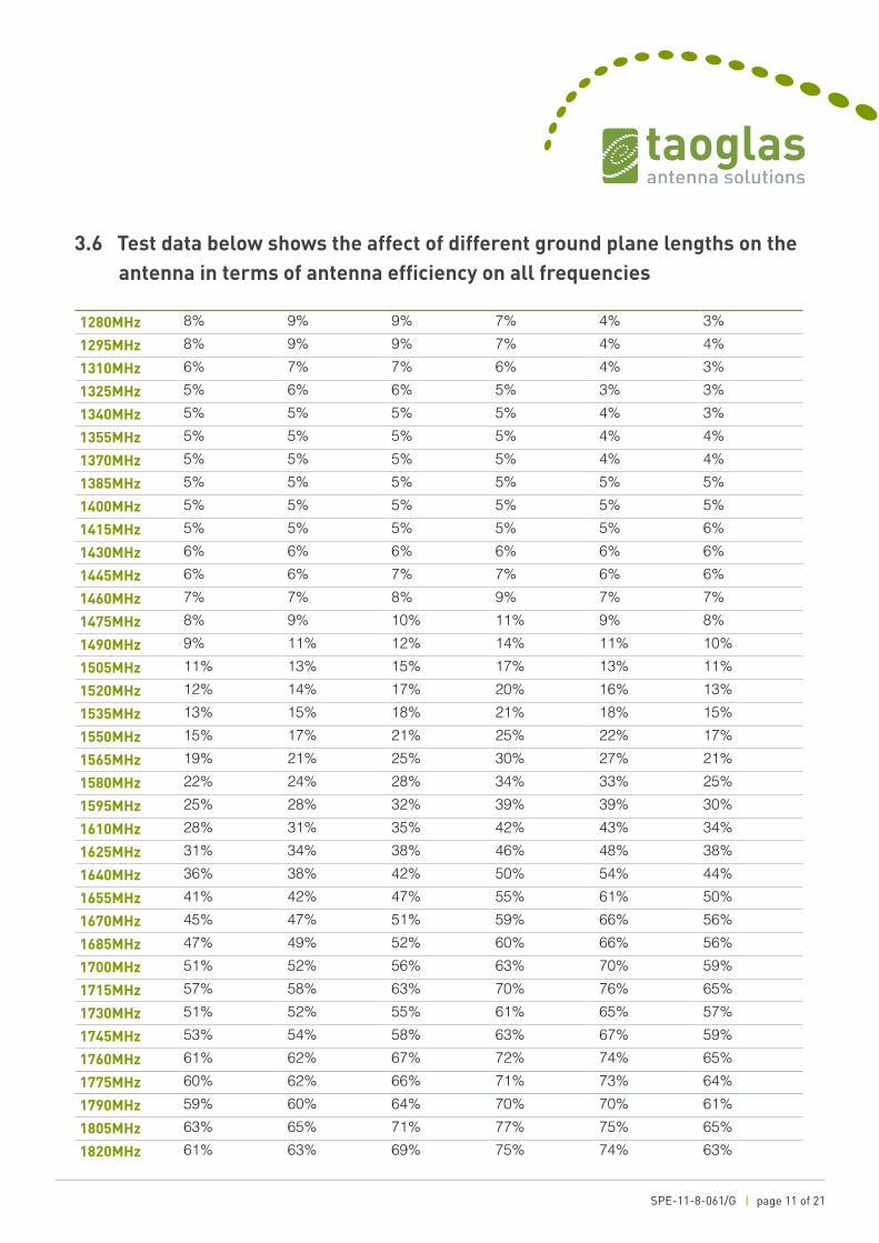
3.6 Test data below shows the affect of different ground plane lengths on the antenna in terms of antenna efficiency on all frequencies
9.5cm 8.5cm 7.5cm 6.5cm 5.5cm 4.5cm
800MHz 51% 33% 24% 18% 11% 10%815MHz 57% 38% 27% 20% 12% 10%830MHz 63% 44% 33% 24% 14% 13%845MHz 70% 51% 39% 29% 17% 15%860MHz 70% 53% 42% 32% 20% 17%875MHz 71% 57% 45% 35% 22% 19%890MHz 65% 53% 42% 33% 20% 17%905MHz 65% 53% 43% 33% 19% 16%920MHz 66% 55% 46% 36% 22% 19%935MHz 68% 57% 48% 38% 23% 20%950MHz 60% 50% 42% 34% 22% 19%965MHz 67% 55% 46% 38% 24% 21%980MHz 65% 54% 45% 37% 23% 20%995MHz 63% 51% 43% 34% 22% 19%1010MHz 64% 52% 43% 35% 22% 20%1025MHz 65% 52% 42% 34% 22% 20%1040MHz 57% 45% 37% 29% 18% 16%1055MHz 58% 45% 36% 28% 18% 16%1070MHz 59% 46% 37% 29% 18% 16%1085MHz 54% 43% 34% 26% 16% 14%1100MHz 52% 41% 32% 24% 14% 13%1115MHz 49% 39% 30% 22% 13% 11%1130MHz 43% 35% 27% 20% 11% 10%1145MHz 38% 32% 24% 18% 10% 8%1160MHz 32% 28% 22% 16% 9% 7%1175MHz 28% 25% 20% 14% 8% 7%1190MHz 26% 24% 19% 14% 7% 6%1205MHz 21% 21% 17% 12% 7% 6%1220MHz 14% 15% 12% 9% 5% 4%1235MHz 13% 14% 12% 9% 5% 4%1250MHz 11% 12% 11% 8% 4% 4%1265MHz 10% 11% 10% 8% 4% 4%
SPE-11-8-061/G | page 11 of 21
3.6 Test data below shows the affect of different ground plane lengths on the antenna in terms of antenna efficiency on all frequencies
1280MHz 8% 9% 9% 7% 4% 3%1295MHz 8% 9% 9% 7% 4% 4%1310MHz 6% 7% 7% 6% 4% 3%1325MHz 5% 6% 6% 5% 3% 3%1340MHz 5% 5% 5% 5% 4% 3%1355MHz 5% 5% 5% 5% 4% 4%1370MHz 5% 5% 5% 5% 4% 4%1385MHz 5% 5% 5% 5% 5% 5%1400MHz 5% 5% 5% 5% 5% 5%1415MHz 5% 5% 5% 5% 5% 6%1430MHz 6% 6% 6% 6% 6% 6%1445MHz 6% 6% 7% 7% 6% 6%1460MHz 7% 7% 8% 9% 7% 7%1475MHz 8% 9% 10% 11% 9% 8%1490MHz 9% 11% 12% 14% 11% 10%1505MHz 11% 13% 15% 17% 13% 11%1520MHz 12% 14% 17% 20% 16% 13%1535MHz 13% 15% 18% 21% 18% 15%1550MHz 15% 17% 21% 25% 22% 17%1565MHz 19% 21% 25% 30% 27% 21%1580MHz 22% 24% 28% 34% 33% 25%1595MHz 25% 28% 32% 39% 39% 30%1610MHz 28% 31% 35% 42% 43% 34%1625MHz 31% 34% 38% 46% 48% 38%1640MHz 36% 38% 42% 50% 54% 44%1655MHz 41% 42% 47% 55% 61% 50%1670MHz 45% 47% 51% 59% 66% 56%1685MHz 47% 49% 52% 60% 66% 56%1700MHz 51% 52% 56% 63% 70% 59%1715MHz 57% 58% 63% 70% 76% 65%1730MHz 51% 52% 55% 61% 65% 57%1745MHz 53% 54% 58% 63% 67% 59%1760MHz 61% 62% 67% 72% 74% 65%1775MHz 60% 62% 66% 71% 73% 64%1790MHz 59% 60% 64% 70% 70% 61%1805MHz 63% 65% 71% 77% 75% 65%1820MHz 61% 63% 69% 75% 74% 63%

SPE-11-8-061/G | page 12 of 21
1835MHz 61% 63% 68% 75% 73% 62%1850MHz 62% 65% 70% 77% 75% 64%1865MHz 63% 66% 72% 80% 77% 64%1880MHz 63% 66% 73% 81% 78% 65%1895MHz 62% 65% 72% 80% 78% 65%1910MHz 60% 62% 68% 77% 75% 62%1925MHz 58% 60% 66% 75% 74% 60%1940MHz 56% 58% 64% 72% 73% 59%1955MHz 54% 55% 61% 69% 71% 58%1970MHz 53% 53% 58% 67% 70% 57%1985MHz 52% 51% 56% 64% 69% 56%2000MHz 51% 50% 54% 62% 68% 55%2015MHz 49% 47% 51% 58% 64% 53%2030MHz 50% 48% 51% 59% 66% 54%2045MHz 48% 45% 47% 54% 62% 52%2060MHz 49% 45% 47% 53% 62% 53%2075MHz 53% 48% 49% 56% 67% 57%2090MHz 54% 48% 49% 56% 66% 58%2105MHz 56% 49% 49% 56% 67% 59%2120MHz 58% 50% 50% 56% 68% 61%2135MHz 58% 51% 50% 55% 66% 61%2150MHz 62% 54% 52% 57% 69% 64%2165MHz 66% 57% 55% 59% 72% 68%2180MHz 65% 56% 53% 56% 68% 66%2195MHz 67% 59% 55% 58% 68% 68%2210MHz 67% 60% 56% 57% 66% 66%2225MHz 66% 60% 56% 57% 63% 64%2240MHz 63% 59% 55% 55% 60% 61%2255MHz 62% 59% 56% 55% 58% 59%2270MHz 63% 61% 58% 57% 57% 58%2285MHz 58% 58% 56% 54% 52% 52%2300MHz 58% 59% 58% 57% 51% 52%
3.6 Test data below shows the affect of different ground plane lengths on the antenna in terms of antenna efficiency on all frequencies

SPE-11-8-061/G | page 13 of 21
4. Drawings
4.1 Layout for the antenna mounting
The size of the ground plane for the complete evaluation board is 97x40 mm. The size of the entire board including the antenna area free of ground plane is 107x40 mm. The area occupied by the antenna is 40x13 mm.

SPE-11-8-061/G | page 14 of 21
4.2 Footprint of antenna

SPE-11-8-061/G | page 15 of 21
4.3 Solder Mask and Solder Areas
To avoid movements of the antenna in the SMD process, we highly recommend to follow the next solder mask and solder pad areas.
The size of the inductor is 0402. The layout has the area to allocate the inductor with a solder land of 0.6x0.5 m for each pad.

SPE-11-8-061/G | page 16 of 21
4.4 Antenna Dimensions
This drawing and its inherent design concepts are property of Taoglas. Not tobe copied or given to third parties without the written consent of Taoglas.
TW Design Centre
Note:1. Week Batch Code Example: 2010 Week 1=01.102.Silver3.Copper4.Ground Clearance Area5. Logo & Text Ink Printing : Black Ground
Feed Line50 Ohm CPW
Footprint0.8t PCB
A ALL Initial Design Jason 2011/6/30
XX-YY
PA-25
Bottom
XX-YY
YearWeek
Top
PA-25
XX-YYPA-25XX-YYPA-25
Ground Clearance Area

SPE-11-8-061/G | page 17 of 21
5. Test Board Dimensions - PAD.25
The test Board is designed for evaluation purposes with a SMA(F) Connector
The size of the ground plane for the complete evaluation board is 97 x 40 mm. The size of the entire board including the antenna area free of ground plane is 110 x 40 mm. The area occupied by the antenna is 13 x 40 mm.

SPE-11-8-061/G | page 18 of 21
5.1 EVB Drawing
Name Material Finish QTY
1 PA.25.A EVB PCB FR4 0.8t Black 12 SMA(F) ST PCB Brass Gold Plated 13 PA.25A Antenna Ceramics White 14 6.8nH Inductor (0402) Ceramics N/A 1

SPE-11-8-061/G | page 19 of 21
6. Transmission Line and Matching Component
A matching component of a 2nH inductor in parallel with PA.25 is required for the PA.25 to have the optimal performance in the evaluation board, located outside of the ground plane in the space specified in the above drawings.
The matching component in a device we recommend starting with a 2.2 nH for short
ground planes (45-75 mm) and 6.8 nH for larger ground planes (80-100 mm). The inductor is strictly required in the antenna integration (this lumped element is considered as part of the antenna).
Is not possible to determine if further improvement in matching is necessary for a PCB in specific, but we recommend
incorporating in the design extra spaces for a “pi” network in between the GSM module and the edge of the ground plane. The starting point will be putting a 0 ohm resistor in series in the “pi” network (S1) and the required 6.8 nH or 2 nH outside of the ground plane (L1). With these spaces we have 3 options for matching topologies as in the next figures:
“pi” matching network
“L” and “Inverted-L” matching network
Further optimization could be done as part of a matching circuit to determine if more components are necessary in the “pi” network, but cannot be determined before, until we test the board with the antenna on it.
Module
Com
pone
nt
Com
pone
nt
Com
pone
nt
S3 S2 L1
Antenna
S1
Component
Ground Plane Limit
Typical config Typical config Component types
Inductor
Capacitor
S3
S1 S1
S2

SPE-11-8-061/G | page 20 of 21
7. Recommended Reflow Temperature Profile
The PA.25 can be assembled following either Sn-Pb or Pb-Free assembly processes. The recommended soldering temperatures are as follows:
Temperature profile – (green area) for the assembly process in reflow ovens
Phase Profile Features Sn-Pb AssemblyPb-Free Assembly (SnAgCu)
Ramp-Up Avg Ramp-Up Rate (Tsmax to Tp) 3°C/second (max) 3°C/second (max)
PreheatTemperature Min (Tsmin)Temperature Max (Tsmax)Time (tsmin to tsmax)
100°C 150°C 60-120 seconds
150°C 200°C 60-120 seconds
Reflow Temperature (TL) Total Time Above TL b(tL)
183°C 60-150 seconds
217°C 60-150 seconds
Peak Temperature (Tp) Time (tp)
235°C 10-30 seconds
260°C 20-40 seconds
Ramp-Down Rate 6°C/second (max) 6°C/second (max)
Time from 25°C to peak Temperature 6 minutes max 8 minutes max
Tem
pera
ture
Time
t 25°C to Peak
Tsmin
Tsmax
Ramp-up
Ramp-down
Critical Zone TL to Tp
ts Preheat
25°
Tp
TL
tp

SPE-11-8-061/G | page 21 of 21
8. Packaging
Taoglas makes no warranties based on the accuracy or completeness of the contents of this document and reserves the right to make changes to specifications and
product descriptions at any time without notice. Taoglas reserves all rights to this document and the information contained herein.
Reproduction, use or disclosure to third parties without express permission is strictly prohibited. Copyright © Taoglas Ltd.
1. Blister tape to IEC 286-3 ’ polyester
2. Pieces/tape: 450