Embed Size (px)
Citation preview

Avnet Embedded. Support Around The Board™
www.avnet-embedded.eu
SpEcificATion
if you require a touch panel solution.For information ontouch sensors, sensor driving and touch panel bonding solutions, scan the QR code or click the URLwww.avnet-embedded.eu/products/displays/.html
LM270WF5
Date: October 2012

Product Specification
LM270WF5 Liquid Crystal Display
Ver 1.0 Oct. 17. 2012 1 / 34
SPECIFICATION FOR
APPROVAL
( ● ) Preliminary Specification ( ) Final Specification
27” Full HD TFT LCD Title
MODEL
BUYER SUPPLIER LG Display Co., Ltd.
*MODEL LM270WF5
SUFFIX SLM1
*When you obtain standard approval,
please use the above model name without suffix
General
APPROVED BY SIGNATURE DATE
/
/
/
Please return 1 copy for your confirmation with
your signature and comments.
W. G. KWEON / G.Manager
MNT Products Engineering Dept. LG Display Co., Ltd.
APPROVED BY SIGNATURE
DATE
REVIEWED BY
PREPARED BY
C. Y. SUNG / Engineer
T. H. SHIN / Manager [P]
Y.S. CHUNG / Manager [M]
H.S. KIM / Manager [C]
Y. G. KANG / Manager [O]

Product Specification
LM270WF5 Liquid Crystal Display
Ver 1.0 Oct. 17. 2012 2 / 34
Contents
No ITEM Page
COVER 1
CONTENTS 2
RECORD OF REVISIONS 3
1 GENERAL DESCRIPTION 4
2 ABSOLUTE MAXIMUM RATINGS 5
3 ELECTRICAL SPECIFICATIONS 6
1) ELECTRICAL CHARACTERISTICS 6
2) INTERFACE CONNECTIONS 9
3) SIGNAL TIMING SPECIFICATIONS 14
4) SIGNAL TIMING WAVEFORMS 15
5) COLOR INPUT DATA REFERNECE 16
6) POWER SEQUENCE 17
7) POWER DIP CONDITION 18
4 OPTICAL SPECIFICATIONS 19
5 MECHANICAL CHARACTERISTICS 27
6 RELIABILITY 30
7 INTERNATIONAL STANDARDS 31
1) SAFETY 31
2) EMC 31
3) Environment 31
8 PACKING 32
1) DESIGNATION OF LOT MARK 32
2) PACKING FORM 32
9 PRECAUTIONS 33
1) MOUNTING PRECAUTIONS 33
2) OPERATING PRECAUTIONS 33
3) ELECTROSTATIC DISCHARGE CONTROL 34
4) PRECAUTIONS FOR STRONG LIGHT EXPOSURE 34
5) STROAGE 34
6) HANDLING PRECAUTIONS FOR PROTECTION FILM 34

Product Specification
LM270WF5 Liquid Crystal Display
Ver 1.0 Oct. 17. 2012 3 / 34
RECORD OF REVISIONS
Revision No Revision Date Page Description
0.0 June. 14. 2012. - First Draft(Preliminary)
0.1 July. 6. 2012 29 Update cover-bottom drawing.
0.2 July. 12. 2012 4 General features ( add Panel type)
29 Add Reverse panel words
33 Add 9-2 operating precautions (11).
0.3 July. 19. 2012 6 Update electrical charictoristics
0.4 July. 24. 2012 4 Update block diagram (reverse type)
6 Update electrical charicteristics
0.5 Aug. 27. 2012. 4,27 Update weight information
4 Update power consumption
6 Update power supply input current / consumption
19 Update Color Coordinates values
28 Update drawing information.
29 Update drawing information.
0.6 Sep. 3. 2012. 6 Change Permissive Power Input Ripple spec (max 200mV 400mV)
24 Update Gray scale step && value (17 step)
0.7 Sep. 11. 2012 29 Update drawing information.
0.8 Sep. 21. 2012 8 Update LED Bar electrical characteristics
0.9 Oct.15.2012 19 Update optical information
1.0 Oct. 17. 2012. 6 Update electrical characteristics ( input current, Power consumption)
Product Specification
LM270WF5 Liquid Crystal Display
Ver 1.0 Oct. 17. 2012 4 / 34
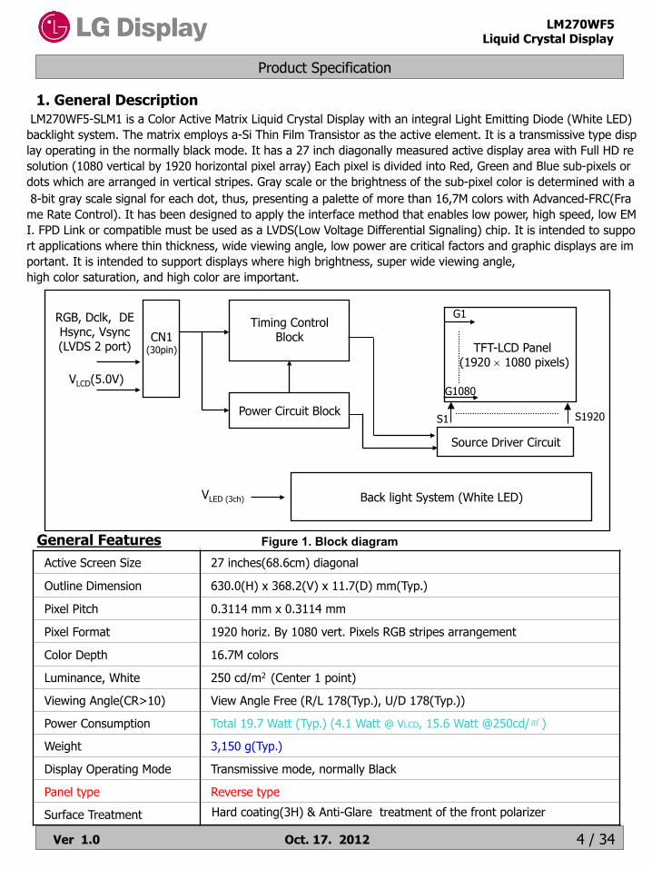
1. General Description
TFT-LCD Panel (1920 1080 pixels)
Source Driver Circuit
Timing Control
Block
Power Circuit Block
CN1 (30pin)
RGB, Dclk, DE Hsync, Vsync (LVDS 2 port)
VLCD(5.0V) G1080
G1
S1920 S1
Back light System (White LED)
Figure 1. Block diagram
VLED (3ch)
LM270WF5-SLM1 is a Color Active Matrix Liquid Crystal Display with an integral Light Emitting Diode (White LED) backlight system. The matrix employs a-Si Thin Film Transistor as the active element. It is a transmissive type display operating in the normally black mode. It has a 27 inch diagonally measured active display area with Full HD resolution (1080 vertical by 1920 horizontal pixel array) Each pixel is divided into Red, Green and Blue sub-pixels or dots which are arranged in vertical stripes. Gray scale or the brightness of the sub-pixel color is determined with a 8-bit gray scale signal for each dot, thus, presenting a palette of more than 16,7M colors with Advanced-FRC(Frame Rate Control). It has been designed to apply the interface method that enables low power, high speed, low EMI. FPD Link or compatible must be used as a LVDS(Low Voltage Differential Signaling) chip. It is intended to support applications where thin thickness, wide viewing angle, low power are critical factors and graphic displays are important. It is intended to support displays where high brightness, super wide viewing angle, high color saturation, and high color are important.
General Features Active Screen Size 27 inches(68.6cm) diagonal
Outline Dimension 630.0(H) x 368.2(V) x 11.7(D) mm(Typ.)
Pixel Pitch 0.3114 mm x 0.3114 mm
Pixel Format 1920 horiz. By 1080 vert. Pixels RGB stripes arrangement
Color Depth 16.7M colors
Luminance, White 250 cd/m2 (Center 1 point)
Viewing Angle(CR>10) View Angle Free (R/L 178(Typ.), U/D 178(Typ.))
Power Consumption Total 19.7 Watt (Typ.) (4.1 Watt @ VLCD, 15.6 Watt @250cd/㎡)
Weight 3,150 g(Typ.)
Display Operating Mode Transmissive mode, normally Black
Panel type Reverse type
Surface Treatment Hard coating(3H) & Anti-Glare treatment of the front polarizer

Product Specification
LM270WF5 Liquid Crystal Display
Ver 1.0 Oct. 17. 2012 5 / 34
90%
10 20 30 40 50 60 70 80 0 -20
0 10
20
30
40
50
Dry Bulb Temperature [℃]
Wet Bulb Temperature [℃]
Storage
Operation
Hum
idity
[(%
)RH
]
10%
40%
60%
60
2. Absolute maximum ratings
The following are maximum values which, if exceeded, may cause faulty operation or damage to the unit.
Note : 1. Temperature and relative humidity range are shown in the figure below. Wet bulb temperature should be 39 °C Max, and no condensation of water. 2. Maximum Storage Humidity is up to 40℃, 70% RH only for 4 corner light leakage Mura. 3. Storage condition is guaranteed under packing condition 4. LCM Surface Temperature should be Min. 0℃ and Max. 65℃ under the VLCD=5.0V, fV=60Hz, 25℃ ambient Temp. no humidity control and LED string current is typical value.
Table 1. Absolute maximum ratings
Parameter Symbol Values
Units Notes Min Max
Power Supply Input Voltage VLCD -0.3 +5.5 Vdc At 25℃
Operating Temperature TOP 0 50 °C
1,2,,3 Storage Temperature TST -20 60 °C
Operating Ambient Humidity HOP 10 90 %RH
Storage Humidity HST 10 90 %RH
LCM Surface Temperature (Operation) Tsurface 0 65 ℃ 1, 4
FIG. 2 Temperature and relative humidity

Product Specification
LM270WF5 Liquid Crystal Display
Ver 1.0 Oct. 17. 2012 6 / 34
3. Electrical Specifications
3-1. Electrical Characteristics
Table 2-1. ELECTRICAL CHARACTERISTICS
Note : 1. Permissive power ripple should be measured under VLCD =5.0V, 25°C, fV(frame frequency)=MAX condition and At that time, we recommend the bandwidth configuration of oscilloscope is to be under 20Mhz. See the next page. 2. The specified current and power consumption are under the VLCD=5.0V, 25± 2°C,fV=60Hz condition whereas Typical Power Pattern [Mosaic] shown in the [ Figure 3 ] is displayed. 3. The current is specified at the maximum current pattern. 4. Maximum Condition of Inrush current : The duration of rush current is about 5ms and rising time of power Input is 500us ± 20%.(min.).
It requires two power inputs. One is employed to power the LCD electronics and to drive the TFT array and liquid crystal. The second input power for the LED/Backlight, is typically generated by a LED Driver. The LED Driver is an external unit to the LCDs.
Parameter Symbol Values
Unit Notes Min Typ Max
MODULE :
Power Supply Input Voltage VLCD 4.5 5 5.5 Vdc
Permissive Power Input Ripple VdRF 400 mVp-p 1
Power Supply Input Current ILCD - 820 1025 mA 2
- 1178 1473 mA 3
Power Consumption Pc TYP - 4.1 5.1 Watt 2
Pc MAX - 5.9 7.4 Watt 3
Rush current IRUSH - 3 A 4

Product Specification
LM270WF5 Liquid Crystal Display
Ver 1.0 Oct. 17. 2012 7 / 34
White pattern Black pattern
• Permissive Power input ripple (VLCD =5.0V, 25°C, fv (frame frequency)=MAX condition)
• Power consumption (VLCD =5V, 25°C, fV (frame frequency=60Hz condition)
Typical power Pattern Maximum power Pattern
FIG.3 Mosaic pattern & Green Pattern for power consumption measurement
Product Specification
LM270WF5 Liquid Crystal Display
Ver 1.0 Oct. 17. 2012 8 / 34
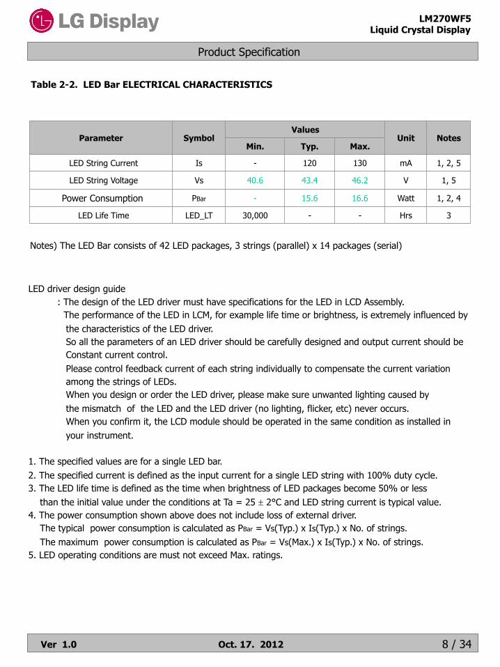
Table 2-2. LED Bar ELECTRICAL CHARACTERISTICS
Parameter Symbol Values
Unit Notes Min. Typ. Max.
LED String Current Is - 120 130 mA 1, 2, 5
LED String Voltage Vs 40.6 43.4 46.2 V 1, 5
Power Consumption PBar - 15.6 16.6 Watt 1, 2, 4
LED Life Time LED_LT 30,000 - - Hrs 3
LED driver design guide : The design of the LED driver must have specifications for the LED in LCD Assembly.
The performance of the LED in LCM, for example life time or brightness, is extremely influenced by the characteristics of the LED driver. So all the parameters of an LED driver should be carefully designed and output current should be Constant current control. Please control feedback current of each string individually to compensate the current variation among the strings of LEDs. When you design or order the LED driver, please make sure unwanted lighting caused by the mismatch of the LED and the LED driver (no lighting, flicker, etc) never occurs. When you confirm it, the LCD module should be operated in the same condition as installed in your instrument. 1. The specified values are for a single LED bar. 2. The specified current is defined as the input current for a single LED string with 100% duty cycle. 3. The LED life time is defined as the time when brightness of LED packages become 50% or less than the initial value under the conditions at Ta = 25 ± 2°C and LED string current is typical value. 4. The power consumption shown above does not include loss of external driver. The typical power consumption is calculated as PBar = Vs(Typ.) x Is(Typ.) x No. of strings. The maximum power consumption is calculated as PBar = Vs(Max.) x Is(Typ.) x No. of strings. 5. LED operating conditions are must not exceed Max. ratings.
Notes) The LED Bar consists of 42 LED packages, 3 strings (parallel) x 14 packages (serial)

Product Specification
LM270WF5 Liquid Crystal Display
Ver 1.0 Oct. 17. 2012
3-2. Interface Connections
Table 3. MODULE CONNECTOR(CN1) PIN CONFIGURATION
3-2-1. LCD Module
Note: 1. All GND(ground) pins should be connected together and to Vss which should also be connected to the LCD’s metal frame. 2. All VLCD (power input) pins should be connected together. 3. Input Level of LVDS signal is based on the IEA 664 Standard. 4. ITLC is Interlace mode selection pin. (L : Normal Mode, H : Interlace mode) If you don’t use this pin, it should be connected to GND.
#1 #30 #1
Rear view of LCM
#30
No Symbol Description No Symbol Symbol
1 FR0M Minus signal of odd channel 0 (LVDS) 16 SR1P Plus signal of even channel 1 (LVDS)
2 FR0P Plus signal of odd channel 0 (LVDS) 17 GND Ground
3 FR1M Minus signal of odd channel 1 (LVDS) 18 SR2M Minus signal of even channel 2 (LVDS)
4 FR1P Plus signal of odd channel 1 (LVDS) 19 SR2P Plus signal of even channel 2 (LVDS)
5 FR2M Minus signal of odd channel 2 (LVDS) 20 SCLKINM Minus signal of even clock channel (LVDS)
6 FR2P Plus signal of odd channel 2 (LVDS) 21 SCLKINP Plus signal of even clock channel (LVDS)
7 GND Ground 22 SR3M Minus signal of even channel 3 (LVDS)
8 FCLKINM Minus signal of odd clock channel (LVDS) 23 SR3P Plus signal of even channel 3 (LVDS)
9 FCLKINP Plus signal of odd clock channel (LVDS) 24 GND Ground
10 FR3M Minus signal of odd channel 3 (LVDS) 25 NC No Connection (I2C Serial interface for LCM)
11 FR3P Plus signal of odd channel 3 (LVDS) 26 NC No Connection.(I2C Serial interface for LCM)
12 SR0M Minus signal of even channel 0 (LVDS) 27 ITLC Interlace mode selection
13 SR0P Plus signal of even channel 0 (LVDS) 28 VLCD Power Supply +5.0V
14 GND Ground 29 VLCD Power Supply +5.0V
15 SR1M Minus signal of even channel 1 (LVDS) 30 VLCD Power Supply +5.0V
- LCD Connector(CN1) : IS100-L30O-C23 (UJU) , GT103-30S-HF15 (LSM) - Mating Connector : FI-X30C2L (Manufactured by JAE) or Equivalent
IS100-L30O-C23
FIG.4 Connector diagram

Product Specification
LM270WF5 Liquid Crystal Display
Ver 1.0 Oct. 17. 2012 10 / 34
Table 4. REQUIRED SIGNAL ASSIGNMENT FOR Flat Link (TI:SN75LVDS83) Transmitter
Pin # Require Signal Pin Name Pin # Require Signal Pin Name
1 Power Supply for TTL Input VCC 29 Ground pin for TTL GND
2 TTL Input (R7) D5 30 TTL Input (DE) D26
3 TTL Input (R5) D6 31 TTL Level clock Input TX CLKIN
4 TTL Input (G0) D7 32 Power Down Input PWR DWN
5 Ground pin for TTL GND 33 Ground pin for PLL PLL GND
6 TTL Input (G1) D8 34 Power Supply for PLL PLL VCC
7 TTL Input (G2) D9 35 Ground pin for PLL PLL GND
8 TTL Input (G6) D10 36 Ground pin for LVDS LVDS GND
9 Power Supply for TTL Input VCC 37 Positive LVDS differential data output 3 TxOUT3+
10 TTL Input (G7) D11 38 Negative LVDS differential data output 3 TxOUT3-
11 TTL Input (G3) D12 39 Positive LVDS differential clock output TX CLKOUT+
12 TTL Input (G4) D13 40 Negative LVDS differential clock output TX CLKOUT-
13 Ground pin for TTL GND 41 Positive LVDS differential data output 2 TX OUT2+
14 TTL Input (G5) D14 42 Negative LVDS differential data output 2 TX OUT2-
15 TTL Input (B0) D15 43 Ground pin for LVDS LVDS GND
16 TTL Input (B6) D16 44 Power Supply for LVDS LVDS VCC
17 Power Supply for TTL Input VCC 45 Positive LVDS differential data output 1 TX OUT1+
46 Negative LVDS differential data output 1 TX OUT1- 18 TTL Input (B7) D17
47 Positive LVDS differential data output 0 TX OUT0+
48 Negative LVDS differential data output 0 TX OUT0-
19 TTL Input (B1) D18
20 TTL Input (B2) D19
49 Ground pin for LVDS LVDS GND 21 Ground pin for TTL Input GND
22 TTL Input (B3) D20
23 TTL Input (B4) D21
50 TTL Input (R6) D27
51 TTL Input (R0) D0
24 TTL Input (B5) D22
25 TTL Input (RSVD) D23
52 TTL Input (R1) D1
53 Ground pin for TTL GND
26 Power Supply for TTL Input VCC 54 TTL Input (R2) D2
55 TTL Input (R3) D3 27 TTL Input (HSYNC) D24
56 TTL Input (R4) D4 28 TTL Input (VSYNC) D25
Notes : 1. Refer to LVDS Transmitter Data Sheet for detail descriptions. 2. 7 means MSB and 0 means LSB at R,G,B pixel data

Product Specification
LM270WF5 Liquid Crystal Display
Ver 1.0 Oct. 17. 2012 11 / 34
LVDS Input characteristics
Description Symbol Min Max Unit Notes
LVDS Clock to Data Skew Margin
tSKEW - 300 + 300 ps 95MHz > Fclk ≥ 85MHz
tSKEW - 400 + 400 ps 85MHz > Fclk ≥ 65MHz
tSKEW - 600 + 600 ps 65MHz > Fclk ≥ 30MHz
LVDS Clock to Clock Skew Margin (Even to Odd)
tSKEW_EO - 1/7 + 1/7 Tclk -
1. DC Specification
2. AC Specification
LVDS +
LVDS -
0V
VCM# |VID| = |(LVDS+) – (LVDS-)|# VCM = {(LVDS+) + (LVDS-)}/2
|VID|
VIN_MAX VIN_MIN
LVDS Data
t SKEW
LVDS Clock
T clk
t SKEW ( F clk = 1 / T clk ) 1 ) 95 MHz > Fclk ≥ 85 MHz : - 300 ~ + 300 2 ) 85 MHz > Fclk ≥ 65 MHz : - 400 ~ + 400 3 ) 65 MHz > Fclk ≥ 30 MHz : - 600 ~ + 600
Description Symbol Min Max Unit Notes
LVDS Differential Voltage |VID| 200 600 mV -
LVDS Common mode Voltage VCM 1.0 1.5 V -
LVDS Input Voltage Range VIN 0.7 1.8 V -
Change in common mode Voltage ΔVCM - 250 mV -

Product Specification
LM270WF5 Liquid Crystal Display
Ver 1.0 Oct. 17. 2012 12 / 34
LVDS Even Data
LVDS Odd Clock
LVDS Even Clock
tSKEW_EO
Tclk
Tclk
< Clock skew margin between channel >
OG0 OR5 OR4 OR3 OR2 OR1 OR0
OB1 OB0 OG5 OG4 OG3 OG2 OG1
DE VSYNC HSYNC OB5 OB4 OB3 OB2
X OB7 OB6 OG7 OG6 OR7 OR6
Current(Nth) CyclePrevious(N-1)th Cycle Next(N+1)th Cycle
RCLK +
RXinO0 +/-
Tclk * 4/7 Tclk * 3/7
Tclk
Tclk * 1/7 MSB R7
R6
R5
R4
R3
R2
R1
R0LSBEG0 ER5 ER4 ER3 ER2 ER1 ER0
EB1 EB0 EG5 EG4 EG3 EG2 EG1
DE VSYNC HSYNC EB5 EB4 EB3 EB2
X EB7 EB6 EG7 EG6 ER7 ER6
* ODD = 1st Pixel EVEN = 2nd Pixel
RXinO1 +/-
RXinO2 +/-
RXinO3 +/-
RXinE0 +/-
RXinE1 +/-
RXinE2 +/-
RXinE3 +/-
OR3 OR2 OR1 OR0
OG4 OG3 OG2 OG1
OB5 OB4 OB3 OB2
OG7 OG6 OR7 OR6
ER3 ER2 ER1 ER0
EG4 EG3 EG2 EG1
EB5 EB4 EB3 EB2
EG7 EG6 ER7 ER6
OG0 OR5 OR4
OB1 OB0 OG5
DE VSYNC HSYNC
X OB7 OB6
EG0 ER5 ER4
EB1 EB0 EG5
DE VSYNC HSYNC
X EB7 EB6
< LVDS Data Format >
3. Data Format 1) LVDS 2 Port

Product Specification
LM270WF5 Liquid Crystal Display
Ver 1.0 Oct. 17. 2012 13 / 34
3-2-2. LED Interface
Table 5. LED connector pin configuration
Pin Symbol Description Notes
1 FB1 Channel1 Current Feedback
2 NC No connection
3 VLED LED Power Supply
4 VLED LED Power Supply
5 FB2 Channel2 Current Feedback
6 FB3 Channel3 Current Feedback
FIG. 5 Backlight connector view
Rear view of LCM
#1
#6
The LED interface connector is a model SM06B-SHJH(HF), wire-locking type manufactured by JST. The mating connector is a SHJP-06V-S(HF) or SHJP-06V-A-K(HF) and Equivalent. The pin configuration for the connector is shown in the table below..

Product Specification
LM270WF5 Liquid Crystal Display
Ver 1.0 Oct. 17. 2012 14 / 32
3-4 Signal timing specifications
Table 7. Timing table
This is the signal timing required at the input of the User connector. All of the interface signal timing should be satisfied with the following specifications for it’s proper operation.
Note: Hsync period and Hsync width-active should be even number times of tCLK. If the value is odd number times of tCLK, display control signal can be asynchronous. In order to operate this LCM a Hsync, Vsyn, and DE(data enable) signals should be used.
1. The performance of the electro-optical characteristics may be influenced by variance of the vertical refresh rates. 2. Vsync and Hsync should be keep the above specification. 3. Hsync Period, Hsync Width, and Horizontal Back Porch should be any times of of character number(4). 4. The polarity of Hsync, Vsync is not restricted. 5. The Max frequency of 1920X1080 resolution is 82.5Mhz
ITEM Symbol Min Typ Max Unit Note
DCLK Period tCLK 11.43 13.89 17.6 ns
Frequency - 57 72 87.5 MHz 5
Hsync
Period tHP 1024 1088 1120 tCLK
Horizontal Valid tHV 960 960 960 tCLK
Horizontal Blank tHB 64 128 160
Frequency fH 64 66 83 KHz
Width tWH 16 32 48 tCLK
Horizontal Back Porch tHBP 32 48 64
Horizontal Front Porch tHFP 16 48 48
Vsync
Period tVP 1090 1100 1160 tHP
Vertical Valid tVV 1080 1080 1080 tHP
Vertical Blank tVB 10 20 80 tHP
Frequency fV 48 60 75 Hz
Width tWV 2 4 16 tHP
Vertical Back Porch tVBP 5 8 32
Vertical Front Porch tVFP 3 8 32

Product Specification
LM270WF5 Liquid Crystal Display
Ver 1.0 Oct. 17. 2012 15 / 34
3-4. Signal Timing Waveforms
DE(Data Enable)
tVV
tVP
DE
DE(Data Enable)
tHP
tHV
DE
1. DCLK , DE, DATA waveforms
2. Horizontal waveform
3. Vertical waveform
tHP
tCLK
Invalid data
Valid data
Invalid data
Invalid data
Invalid data
Pixel 0,0 Pixel 2,0
Pixel 1,0 Pixel 3,0
DE(Data Enable)
Valid data
DCLK
First data
Second data

Product Specification
LM270WF5 Liquid Crystal Display
Ver 1.0 Oct. 17. 2012 16 / 34
3-5. Color Input Data Reference
Table 7. COLOR DATA REFERENCE
The Brightness of each primary color(red,green,blue) is based on the 8-bit gray scale data input for the color; the higher the binary input, the brighter the color. The table below provides a reference for color versus data input.
Color
Input Color Data
RED MSB LSB
GREEN MSB LSB
BLUE MSB LSB
R7 R6 R5 R4 R3 R2 R1 R0 G7 G6 G5 G4 G3 G2 G1 G0 B7 B6 B5 B4 B3 B2 B1 B0
Basic Color
Black 0 0 0 0 0 0 0 0 0 0 0 0 0 0 0 0 0 0 0 0 0 0 0 0
Red (255) 1 1 1 1 1 1 1 1 0 0 0 0 0 0 0 0 0 0 0 0 0 0 0 0
Green (255) 0 0 0 0 0 0 0 0 1 1 1 1 1 1 1 1 0 0 0 0 0 0 0 0
Blue (255) 0 0 0 0 0 0 0 0 0 0 0 0 0 0 0 0 1 1 1 1 1 1 1 1
Cyan 0 0 0 0 0 0 0 0 1 1 1 1 1 1 1 1 1 1 1 1 1 1 1 1
Magenta 1 1 1 1 1 1 1 1 0 0 0 0 0 0 0 0 1 1 1 1 1 1 1 1
Yellow 1 1 1 1 1 1 1 1 1 1 1 1 1 1 1 1 0 0 0 0 0 0 0 0
White 1 1 1 1 1 1 1 1 1 1 1 1 1 1 1 1 1 1 1 1 1 1 1 1
RED
RED (000) Dark 0 0 0 0 0 0 0 0 0 0 0 0 0 0 0 0 0 0 0 0 0 0 0 0
RED (001) 0 0 0 0 0 0 0 1 0 0 0 0 0 0 0 0 0 0 0 0 0 0 0 0
... ... ... ...
RED (254) 1 1 1 1 1 1 1 0 0 0 0 0 0 0 0 0 0 0 0 0 0 0 0 0
RED (255) 1 1 1 1 1 1 1 1 0 0 0 0 0 0 0 0 0 0 0 0 0 0 0 0
GREEN
GREEN (000) Dark 0 0 0 0 0 0 0 0 0 0 0 0 0 0 0 0 0 0 0 0 0 0 0 0
GREEN (001) 0 0 0 0 0 0 0 0 0 0 0 0 0 0 0 1 0 0 0 0 0 0 0 0
... ... ... ...
GREEN (254) 0 0 0 0 0 0 0 0 1 1 1 1 1 1 1 0 0 0 0 0 0 0 0 0
GREEN (255) 0 0 0 0 0 0 0 0 1 1 1 1 1 1 1 1 0 0 0 0 0 0 0 0
BLUE
BLUE (000) Dark 0 0 0 0 0 0 0 0 0 0 0 0 0 0 0 0 0 0 0 0 0 0 0 0
BLUE (001) 0 0 0 0 0 0 0 0 0 0 0 0 0 0 0 0 0 0 0 0 0 0 0 1
... ... ... ...
BLUE (254) 0 0 0 0 0 0 0 0 0 0 0 0 0 0 0 0 1 1 1 1 1 1 1 0
BLUE (255) 0 0 0 0 0 0 0 0 0 0 0 0 0 0 0 0 1 1 1 1 1 1 1 1

Product Specification
LM270WF5 Liquid Crystal Display
Ver 1.0 Oct. 17. 2012 17 / 34
Notes : 1. Please VLCD power on only after connecting interface cable to LCD. 2. Please avoid floating state of interface signal at invalid period. 3. When the interface signal is invalid, be sure to pull down the power supply for LCD VLCD to 0V. 4. LED power must be turn on after power supply for LCD an interface signal are valid.
Parameter Values
Units Min Typ Max
T1 0.5 - 10 ms
T2 0.01 - 50 ms
T3 500 - - ms
T4 200 - - ms
T5 0.01 - 50 ms
T7 1000 - ms
Table 8. POWER SEQUENCE
10%
90% 90%
10%
T1 T2 T5 T7
T3 T4
Valid data
LED on
0V
OFF OFF
Power supply for LCD Vcc
Interface signal VI
Power Supply for LED
3-5. Power sequence

Product Specification
LM270WF5 Liquid Crystal Display
Ver 1.0 Oct. 17. 2012 18 / 34
3-7. VLCD Power Dip Condition
1) Dip condition
3.5V ≤VLCD< 4.5V , td≤20ms 2) VLCD< 3.5V VLCD-dip conditions should also follow the Power On/Off conditions for supply voltage.
4.5V
3.5V
VLCD
td
FIG.6 Power dip condition
GND(ground)

Product Specification
LM270WF5 Liquid Crystal Display
Ver 1.0 Oct. 17. 2012 19 / 34
Optical characteristics are determined after the unit has been ‘ON’ for approximately 30 minutes in a dark environment at 25±2°C. The values specified are at an approximate distance 50cm from the LCD surface at a viewing angle of and equal to 0 ° and aperture 1 degree. FIG. 1 presents additional information concerning the measurement equipment and method.
4. Optical Specifications
50cm
Optical Stage(x,y) LCD Module PR 880 or RD 80S
or PR650
Table 9. OPTICAL CHARACTERISTICS
FIG.7 Optical Characteristic Measurement Equipment and Method
Parameter Symbol Values
Units Notes Min Typ Max
Contrast Ratio CR 600 1000 - 1 Surface Luminance, white LWH 200 250 - cd/m2 2 Luminance Variation WHITE 75 - - % 3
Response Time Gray To Gray TGTG_AVR - 14 25 ms 4 Gray-to-Gray (BW)
G to G BW - 8 - ms Reference
10
Color Coordinates [CIE1931] (By PR650)
RED Rx
Typ -0.03
0.653
Typ +0.03
Ry 0.337 GREEN Gx 0.320
Gy 0.612 BLUE Bx 0.150
By 0.068 WHITE Wx 0.313
Wy 0.329 Color Shift (Avg. Δu’v’ < 0.02)
Horizontal CST_H - 140 - Degree 5
Vertical CST_V - 100 - Viewing Angle (CR>10)
General Horizontal H 170 178 -
Degree 6 Vertical V 170 178 -
Color gamut (CG, CIE1931) - 72 - % Luminance uniformity – Angular dependence (TCO 5.1)
LR - - 1.73 11
Color uniformity Angular dependence( TCO 5.1)
0.025 12
Gray Scale - 2.2 9
(Ta=25 °C, VLCD=5V, fV=60Hz Dclk=144MHz, IBL=120 mA)
4-1. 2D Optical specifications

Product Specification
LM270WF5 Liquid Crystal Display
Ver 1.0 Oct. 17. 2012 20 / 34
Notes 1. Contrast Ratio(CR) is defined mathematically as : (By PR880)
It is measured at center point(Location P1) 2. Surface luminance(LWH)is luminance value at Center 1 point(P1) across the LCD surface 50cm fro
m the surface with all pixels displaying white. For more information see FIG.8 (By PR880) 3. The variation in surface luminance , WHITE is defined as : (By PR880) Where L1 to L9 are the luminance with all pixels displaying white at 9 locations.
For more information see FIG.8 4. Gray to gray response time is the time required for the display to transition from gray to gray. For
additional information see Table 10. (By RD80S) 5. Color shift is the angle at which the average color difference for all Macbeth is lower than 0.02. For more information see FIG.9 (By EZ Contrast) - Color difference (Δu’v’) u’1, v’1 : u’v’ value at viewing angle direction u’2, v’2 : u’v’ value at front (θ=0) i : Macbeth chart number (Define 23 page) - Pattern size : 25% Box size - Viewing angle direction of color shift : Horizontal, Vertical 6. Viewing angle is the angle at which the contrast ratio is greater than 10. The angles are determined for the horizontal or x axis and the vertical or y axis with respect to the z axis which is normal to the LCD surface. For more information see FIG.10 (By PR880) 7. GSR is the rate of gamma shift at up, down, left and right 60 degree viewing angle compare with
center gamma. For more information see FIG.11 and FIG.12 (By EZ Contrast) - GSR ( Gamma ) is defined as : . 8. WPT (White Point Tracking) is the variation of color temperature between G255 and G63. (By PR650)
3122
4'
++−=
yx
xu
3122
9'
++−=
yx
yv 2
212
21 )''()''('' vvuuvu −+−=Δ
pixelsblack all with Luminance Surface
pixels whiteall with Luminance SurfaceRatioContrast =
100)L .... ,L ,(L Maximum)L .. ,L,Minimum(L
P9P2P1
P9P2P1 ×…
=WHITEδ
24
)''()''(
24
1∑=
Δ=Δ i
ivuvuAvg
100Degree) (0 Value GammaCenter
Degree) 60Light Reft, Down, (Up, Value Gamma angle View1 ×⎟⎟
⎠
⎞⎜⎜⎝
⎛−=GSR

Product Specification
LM270WF5 Liquid Crystal Display
Ver 1.0 Oct. 17. 2012 21 / 34
Table. 10 GTG Gray Table
Measuring point for surface luminance & measuring point for luminance variation.
H
H/2
V
V/2
●
P1
P4 P2
P9 P7
●
●
● ●
●P3
●P8
P6 ●
P5 ●
H/10
V/10
Gray to Gray Rising Time
G255 G191 G127 G63 G0
Falling Time G255
G191
G127
G63
G0
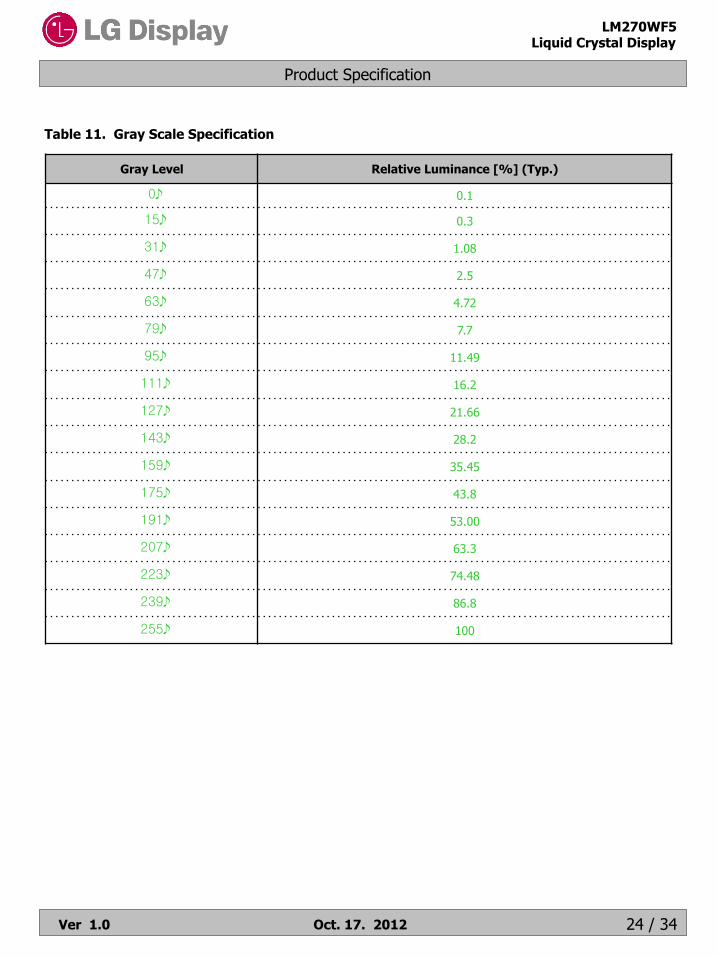
Notes 9. Gamma Value is approximately 2.2. For more information see Table 11.
The Gray to Gray response time is defined as the following figure and shall be measured by switching the input signal for “Gray To Gray “. - Gray step : 5 Step - TGTG_AVR is the total average time at rising time and falling time for “Gray To Gray “. - if system use ODC ( Over Driving Circuit) function, Gray to Gary response time may be 5ms~8ms GtG * it depends on Overshoot rate.
FIG.8 Measure Point for Luminance
Notes 10. Response time is the time required for the display to transit from any gray to white (Rise Time, TrR) and from any gray to black (Decay time, TrD). G to GBW Spec stands for average value of all measured points. (By RD80S)

Product Specification
LM270WF5 Liquid Crystal Display
Ver 1.0 Oct. 17. 2012 22 / 34
25% Box size
Dark skin (i=1) Light skin Blue sky Foliage Blue flower Bluish green
R 98 206 85 77 129 114
G 56 142 112 102 118 199
B 45 123 161 46 185 178
Orange Purplish blue Moderate red Purple Yellow green Orange yellow
R 219 56 211 76 160 230
G 104 69 67 39 193 162
B 24 174 87 86 58 29
Blue Green Red Yellow Magenta Cyan
R 26 72 197 241 207 35
G 32 148 27 212 62 126
B 145 65 37 36 151 172
White Neutral 8 Neutral 6.5 Neutral 5 Neutral 3.5 Black
R 240 206 155 110 63 22
G 240 206 155 110 63 22
B 240 206 155 110 63 22
Average RGB values in Bruce RGB for Macbeth Chart
Color shift is defined as the following test pattern and color.
FIG.9 Color Shift Test Pattern
White Gray(N)
Tr Tf 100 90
10
0
Optical Response
N = 0(Black)~255(White) Gray(N) Black
G to G(BW) Response time is defined as the following figure and shall be measured by switching the input signal for “Gray(N)” and “Black or White”.

Product Specification
LM270WF5 Liquid Crystal Display
Ver 1.0 Oct. 17. 2012 23 / 34
Dimension of viewing angle range.
Normal
Y E
φ
θ
φ = 0°, Right
φ = 180°, Left
φ = 270°, Down
φ = 90°, Up
br LaVL += )log()log()log( aVrLL b +=−
Here the Parameter α and γ relate the signal level V to the luminance L. The GAMMA we calculate from the log-log representation (FIG.11)
FIG.11 Sample Luminance vs. gray scale (using a 256 bit gray scale)
FIG.12 Sample Log-log plot of luminance vs. gray scale
FIG.10 Viewing angle
Product Specification
LM270WF5 Liquid Crystal Display
Ver 1.0 Oct. 17. 2012 24 / 34
Table 11. Gray Scale Specification
Gray Level Relative Luminance [%] (Typ.)
0 0.1
15 0.3
31 1.08
47 2.5
63 4.72
79 7.7
95 11.49
111 16.2
127 21.66
143 28.2
159 35.45
175 43.8
191 53.00
207 63.3
223 74.48
239 86.8
255 100

Product Specification
LM270WF5 Liquid Crystal Display
Ver 1.0 Oct. 17. 2012 25 / 34
Notes 11 : Luminance Uniformity - angular – dependence (LR& TB)
TCO 5.0 Luminance uniformity – angular dependence, is the capacity of the VDU to present the same Luminance level independently of the viewing direction. The angular-dependent luminance uniformity is calculated as the ratio of maximum luminance to minimum luminance in the specified measurement areas. - Test pattern : Full white 4˚× 4˚square size, back ground shall be set to 80% image loading, RGB 204, 204, 204 - Test luminance : ≥200cd/㎡ - Test point : 5-point - Test distance : D * 1.5 - Test method : LR = ((Lmax.+30deg. / Lmin. +30deg.) + (Lmax. -30deg. / Lmin. -30deg.)) / 2 TB = ((Lmax.+15deg. / Lmin. +15deg.)
< Luminance uniformity - angular dependence measuring point >
FIG. 13 Luminance Uniformity angular dependence
H
V
H/10
V/2
H/2
V/10
V/10
H/10
D

Product Specification
LM270WF5 Liquid Crystal Display
Ver 1.0 Oct. 17. 2012 26 / 34
Note 12 :. Colour uniformity Angular dependence (LR)
TCO 5.0 Color uniformity – angular dependence, is the capacity of the VDU to present the same Colour level independently of the viewing direction. The angular-dependent colour uniformity is calculated as the largest difference in △u'v' value - Test pattern : Full white 4˚× 4˚square size, back ground shall be set to 80% image loading, RGB 204, 204, 204 - Test luminance : ≥200cd/㎡ - Test point : 3-point - Test distance : D * 1.5 - Test method 1. The screen shall then be rotated ±30 degrees around a vertical axis through the screen centre-point and the chromaticity co-ordinates at positions PL, PR, (u'PL/ ± 30º, v'PL/ ± 30º and u' PR/ ± 30º, v'PR/ ± 30º respectively) shall be recorded. 2. △u’v’ shall be calculated for each measured position using the formula a. △u’v’+30º =((u'PL/ + 30º - u' PR/ + 30º)2+(v'PL/ + 30º - v'PR/ +30º )2)^1/2
b. △u’v-30º =((u'PL/ - 30º - u' PR/ - 30º)2+(v'PL/ - 30º - v'PR/ -30º )2)^1/2 3. The largest difference in △ u'v' value shall be reported
< Colour uniformity - angular dependence measuring point >
FIG. 14 Colour uniformity Angular dependence
H
V
H/10
V/2
H/2
H/10
D PL PC PR

Product Specification
LM270WF5 Liquid Crystal Display
Ver 1.0 Oct. 17. 2012 27 / 34
5. Mechanical Characteristics
The contents provide general mechanical characteristics. In addition the figures in the next page are detailed mechanical drawing of the LCD.
Notes : Please refer to a mechanic drawing in terms of tolerance at the next page.
Outline Dimension
Horizontal 630mm
Vertical 368.2mm
Depth 11.7mm
Bezel Area Horizontal 602mm
Vertical 340.4mm
Active Display Area Horizontal 597.888mm
Vertical 336.312mm
Weight Typ : 3,150, Max : 3,310
Surface Treatment Hard coating(3H) Anti-Glare treatment of the front polarizer

Product Specification
LM270WF5 Liquid Crystal Display
Ver 1.0 Oct. 17. 2012
<FRONT VIEW>

Product Specification
LM270WF5 Liquid Crystal Display
Ver 1.0 Oct. 17. 2012
* Reverse Panel <REAR VIEW>

Product Specification
LM270WF5 Liquid Crystal Display
Ver 1.0 Oct. 17. 2012 30 / 34
6. Reliability
Environment test condition
No Test Item Condition
1 High temperature storage test Ta= 60°C 240h
2 Low temperature storage test Ta= -20°C 240h
3 High temperature operation test Ta= 50°C 50%RH 240h
4 Low temperature operation test Ta= 0°C 240h
5 Vibration test (non-operating)
Wave form : random Vibration level : 1.00G RMS Bandwidth : 10-300Hz Duration : X, Y, Z, 10 min One time each direction
6 Shock test (non-operating)
Shock level : 100G Waveform : half sine wave, 2ms Direction : ±X, ±Y, ±Z One time each direction
7 Humidity condition Operation Ta= 40 °C ,90%RH
8 Altitude operating storage / shipment
0 - 16,400 feet(5,000m) 0 - 40,000 feet(12,192m)
9 Maximum Storage Humidity for 4 corner light leakage Mura. Max 70%RH , Ta=40℃

Product Specification
LM270WF5 Liquid Crystal Display
Ver 1.0 Oct. 17. 2012 31 / 34
7. International Standards
7-2. EMC
7-3. Environment
a) ANSI C63.4 “American National Standard for Methods of Measurement of Radio-Noise Emissions from Low-Voltage Electrical and Electronic Equipment in the Range of 9 kHz to 40 GHz.” American National Standards Institute (ANSI), 2003.
b) CISPR 22 “Information technology equipment – Radio disturbance characteristics – Limit and methods of measurement." International Special Committee on Radio Interference (CISPR), 2005.
c) CISPR 13 “Sound and television broadcast receivers and associated equipment – Radio disturbance characteristics – Limits and method of measurement." International Special Committee on Radio Interference (CISPR), 2006.
a) RoHS, Directive 2002/95/EC of the European Parliament and of the council of 27 January 2003
7-1. Safety
Class 1M LED Product IEC60825-1 : 2001
Embedded LED Power (Class1M)
Notes 1. Laser (LED Backlight) Information
2. Caution : LED inside. Class 1M laser (LEDs) radiation when open. Do not open while operating.
c) EN 60950-1, European Committee for Electrotechnical Standardization (CENELEC). Information Technology Equipment - Safety - Part 1 : General Requirements.
a) UL 60950-1, Underwriters Laboratories Inc. Information Technology Equipment - Safety - Part 1 : General Requirements. b) CAN/CSA C22.2 No.60950-1-07, Canadian Standards Association. Information Technology Equipment - Safety - Part 1 : General Requirements.
d) IEC 60950-1, The International Electrotechnical Commission (IEC). Information Technology Equipment - Safety - Part 1 : General Requirements. (Including report of IEC60825-1:2001 clause 8 and clause 9)
Product Specification
LM270WF5 Liquid Crystal Display
Ver 1.0 Oct. 17. 2012 32 / 34
8-2. Packing Form
a) Package quantity in one box : 10-LCMs ( 1 Module is packed in 1 AL Bag ) b) Box Size : 700(L) X 355(W) X 430(H)
8. Packing
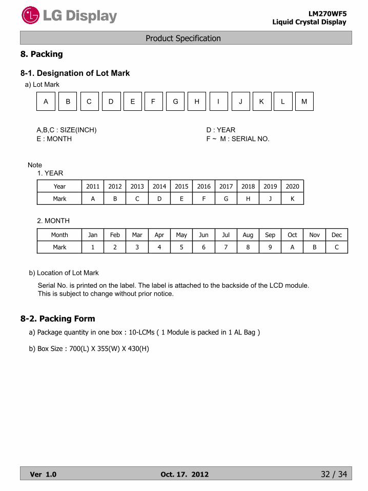
8-1. Designation of Lot Mark a) Lot Mark
A B C D E F G H I J K L M
A,B,C : SIZE(INCH) D : YEAR E : MONTH F ~ M : SERIAL NO.
Note 1. YEAR
2. MONTH
Mark
Year
K
2020
F
2016
G
2017
H
2018
J
2019
D
2014
E
2015
C B A
2013 2012 2011
B
Nov
Mark
Month
A
Oct
6
Jun
7
Jul
8
Aug
9
Sep
4
Apr
5
May
C 3 2 1
Dec Mar Feb Jan
b) Location of Lot Mark
Serial No. is printed on the label. The label is attached to the backside of the LCD module. This is subject to change without prior notice.

Product Specification
LM270WF5 Liquid Crystal Display
Ver 1.0 Oct. 17. 2012 33 / 34
9. PRECAUTIONS
Please pay attention to the followings when you use this TFT LCD module.
9-1. MOUNTING PRECAUTIONS
(1) You must mount a module using holes arranged in four corners or four sides. (2) You should consider the mounting structure so that uneven force (ex. Twisted stress) is not applied to the module. And the case on which a module is mounted should have sufficient strength so that external
force is not transmitted directly to the module. (3) Please attach the surface transparent protective plate to the surface in order to protect the polarizer. Transparent protective plate should have sufficient strength in order to the resist external force. (4) You should adopt radiation structure to satisfy the temperature specification. (5) Acetic acid type and chlorine type materials for the cover case are not desirable because the former generates corrosive gas of attacking the polarizer at high temperature and the latter causes circuit break
by electro-chemical reaction. (6) Do not touch, push or rub the exposed polarizers with glass, tweezers or anything harder than HB pencil lead. And please do not rub with dust clothes with chemical treatment. Do not touch the surface of polarizer for bare hand or greasy cloth.(Some cosmetics are detrimental to the polarizer.) (7) When the surface becomes dusty, please wipe gently with absorbent cotton or other soft materials like
chamois soaks with petroleum benzene. Normal-hexane is recommended for cleaning the adhesives used to attach front / rear polarizers. Do not use acetone, toluene and alcohol because they cause chemical damage to the polarizer.
(8) Wipe off saliva or water drops as soon as possible. Their long time contact with polarizer causes deformations and color fading.
(9) Do not open the case because inside circuits do not have sufficient strength. (10) As The IPS panel is sensitive & slim, please recommend the metal frame of the system supports the panel by the double side-mount. 9-2. OPERATING PRECAUTIONS (1) The spike noise causes the mis-operation of circuits. It should be lower than following voltage :
V=±200mV(Over and under shoot voltage) (2) Response time depends on the temperature.(In lower temperature, it becomes longer.) (3) Brightness depends on the temperature. (In lower temperature, it becomes lower.) And in lower temperature, response time(required time that brightness is stable after turned on) becomes longer. (4) Be careful for condensation at sudden temperature change. Condensation makes damage to polarizer or
electrical contacted parts. And after fading condensation, smear or spot will occur. (5) When fixed patterns are displayed for a long time, remnant image is likely to occur. (6) Module has high frequency circuits. Sufficient suppression to the electromagnetic interference shall be
done by system manufacturers. Grounding and shielding methods may be important to minimized the interference. (7) Please do not give any mechanical and/or acoustical impact to LCM. Otherwise, LCM can’t be operated its full characteristics perfectly. (8) A screw which is fastened up the steels should be a machine screw. (if not, it causes metallic foreign material and deal LCM a fatal blow) (9) Please do not set LCD on its edge. (10) When LCMs are used for public display defects such as Yogore, image sticking can not guarantee. (11) When this reverse model is used as a forward-type model(PCB on top side), LGD can not guarantee any defects of LCM. (12) LCMs cannot support “Interlaced Scan Method”

Product Specification
LM270WF5 Liquid Crystal Display
Ver 1.0 Oct. 17. 2012 34 / 34
Since a module is composed of electronic circuits, it is not strong to electrostatic discharge. Make certain that treatment persons are connected to ground through wrist band etc. And don’t touch interface pin directly.
9-3. ELECTROSTATIC DISCHARGE CONTROL
Strong light exposure causes degradation of polarizer and color filter.
9-4. PRECAUTIONS FOR STRONG LIGHT EXPOSURE
When storing modules as spares for a long time, the following precautions are necessary. (1) Store them in a dark place. Do not expose the module to sunlight or fluorescent light. Keep the temperature between 5°C and 35°C at normal humidity. (2) The polarizer surface should not come in contact with any other object. It is recommended that they be stored in the container in which they were shipped.
9-5. STORAGE
9-6. HANDLING PRECAUTIONS FOR PROTECTION FILM
(1) The protection film is attached to the bezel with a small masking tape. When the protection film is peeled off, static electricity is generated between the film and polarizer. This should be peeled off slowly and carefully by people who are electrically grounded and with well ion- blown equipment or in such a condition, etc. (2) When the module with protection film attached is stored for a long time, sometimes there remains a very small amount of glue still on the bezel after the protection film is peeled off. (3) You can remove the glue easily. When the glue remains on the bezel surface or its vestige is recognized, please wipe them off with absorbent cotton waste or other soft material like chamois soaked with normal- hexane.

AvnET EmBEddEd officES
dEnmArkAvnet EmbeddedAvnet Nortec A/SEllekær 92730 HerlevPhone: +45 3678 6250Fax: +45 3678 [email protected]
finlAndAvnet EmbeddedAvnet Nortec OyPihatörmä 1 B02240 EspooPhone: +358 20 749 9 260Fax: +358 20 749 9 [email protected]
frAncEAvnet EmbeddedAvnet EMG France SAParc Club du Moulin à Vent, Bât 1033, rue du Dr Georges Lévy 69693 Vénissieux CedexPhone: +33 4 78 77 13 92Fax: +33 4 78 77 13 [email protected]
Avnet EmbeddedAvnet EMG France SA14 avenue Carnot 91349 Massy Cedex Phone: +33 1 64 47 29 29Fax: +33 1 64 47 99 [email protected]
Avnet EmbeddedAvnet EMG France SALes Peupliers II35 avenue des Peupliers35510 Cesson-SévignéPhone: + 33 2 99 77 37 02Fax: + 33 2 99 77 37 [email protected]
GErmAnY (AUSTriA, cZEcH rEpUBlic, HUnGArY, polAnd, SWiTZErlAnd)Avnet EmbeddedAvnet EMG GmbHGruber Straße 60c85586 PoingPhone: +49 8121 775 500 Fax: +49 8121 775 [email protected]
Avnet EmbeddedAvnet EMG GmbHLötscher Weg 6641334 NettetalPhone: +49 8121 775 500Fax: +49 8121 775 [email protected]
iTAlY (porTUGAl, SpAin)Avnet EmbeddedAvnet EMG Italy SRLVia Manzoni, 4420095 Cusano MilaninoPhone: +39 02 660 92 1Fax: +39 02 660 92 [email protected]
nETHErlAndS (BElGiUm, lUXEmBoUrG)Avnet EmbeddedAvnet B.V.Takkebijsters 24817 BL BredaPhone: +31 76 5722400Fax: +31 76 [email protected]
SWEdEn (norWAY)Avnet EmbeddedAvnet Nortec ABEsplanaden 3 D172 67 SundbybergPhone: +46 8 564 725 50Fax: +46 8 760 01 [email protected]
UniTEd kinGdom (irElAnd)Avnet Embedded5a Waltham ParkWhite WalthamMaidenheadBerkshire, SL6 3TNPhone: +44 1628 518900Fax: +44 1628 [email protected]
www.avnet-embedded.eu
02/2013
All trademarks and logos are the property of their respective owners. No guarentee as to the accuracy, completeness or reliability of any information. Subject to modifications and amendments.