Embed Size (px)
Citation preview
Enclustra GmbH
Räffelstrasse 28 – CH-8045 Zürich – Switzerland
Phone +41 43 343 39 43 – www.enclustra.com
1
Application Examples
Avnet Silica & Enclustra Seminar “Getting started with Xilinx Zynq SoC”
Fribourg, April 26, 2017

Enclustra GmbH
Räffelstrasse 28 – CH-8045 Zürich – Switzerland
Phone +41 43 343 39 43 – www.enclustra.com
2
Application Examples
Avnet Silica & Enclustra Seminar “Getting started with Xilinx Zynq SoC”
Fribourg, April 26, 2017
Enclustra GmbH
Räffelstrasse 28 – CH-8045 Zürich – Switzerland
Phone +41 43 343 39 43 – www.enclustra.com
3
Application Examples
Avnet Silica & Enclustra Seminar “Getting started with Xilinx Zynq SoC”
Fribourg, April 26, 2017
Introduction
The next few slides give a brief overview of what will be discussed in this presentation
and they contain some general points that apply to both examples covered.
The presentation does not only highlight the implementation of the projects
discussed but it points out as well what know-how is required to successfully realize
an offloading engine using FPGA fabric within an SoC.

Enclustra GmbH
Räffelstrasse 28 – CH-8045 Zürich – Switzerland
Phone +41 43 343 39 43 – www.enclustra.com
4
Application Examples
Avnet Silica & Enclustra Seminar “Getting started with Xilinx Zynq SoC”
Fribourg, April 26, 2017
Projects Discussed
Two very different projects are discussed in this presentation.
The first project is a statistical image processing engine whose only purpose is to
accelerate an algorithm already implemented in software. Since the customer is
doing statistical image processing regularly, the engine has to be designed in a
reusable way. The algorithms to speed up were known when the project started, so
the operations to implement were specified exactly and Enclustra was only
responsible for converting the operations into a form that can be implemented in
SoC fabric easily (fixed-point-quantization, approximations, etc.).
The second project is a Bluetooth transceiver. It allows receiving and transmitting
packets. All link-layer operations (data encoding, header generation, etc.) and
physical-layer operations (modulation, demodulation, filtering, etc.) are executed
within the offloading engine. The algorithms were developed by Enclustra since the
customer has a lot of knowledge in protocol handling but less knowledge in digital
signal processing. Because the requirements are very project specific, the transceiver
is not optimized for reusage.
There is one point both example projects have in common: They are both fixed-point
math intensive.

Enclustra GmbH
Räffelstrasse 28 – CH-8045 Zürich – Switzerland
Phone +41 43 343 39 43 – www.enclustra.com
5
Application Examples
Avnet Silica & Enclustra Seminar “Getting started with Xilinx Zynq SoC”
Fribourg, April 26, 2017
Enclustra Fixed-Point Math Development Flow
To understand the examples discussed in this presentation, a basic knowledge about the
development flow used for both projects is required. Therefore this flow is described briefly.
Almost every engineer made the experience that written language (or even worse: spoken
language) is prone to misunderstandings. Moreover language does not enforce the
specification of all corner cases, which leads to unclear requirements. Nevertheless, written
language is used for most specifications. This introduces significant risk for both sides, the
customer (delay) and Enclustra as service company (rework effort).
In some cases, customers are already aware of these problems and provide a MATLAB,
Simulink or C implementation of the algorithm to be implemented in an FPGA or SoC. Even
though this solves the problem of misunderstandings regarding the specification, the
algorithms provided are often using double precision floating point numbers which are not
implementable efficiently in FPGA fabric. As a result the algorithm must be changed to work
with fixed-point operations and other implementation-optimized concepts such as taylor
approximations for functions. This conversion leads to slight changes in the behavior and
therefore again to the risk that the algorithm does not perform as expected and rework is
required.
To reduce the risk described above, Enclustra always implements a fixed-point model of the
algorithm in such a way that it can be implemented bit-true in the FPGA fabric. The customer
can then analyze the performance of the algorithm and identify changes required to meet all
requirements before the implementation is started. After approval by the customer, the bit-
true model of the algorithm is used as specification for the implementation.
This approach significantly reduces risk for both sides and improves work efficiency since a
100% clear an implementable specification in a programming language (usually MATLAB)
exists when the implementation of the offloading engine is started.
Enclustra GmbH
Räffelstrasse 28 – CH-8045 Zürich – Switzerland
Phone +41 43 343 39 43 – www.enclustra.com
6
Application Examples
Avnet Silica & Enclustra Seminar “Getting started with Xilinx Zynq SoC”
Fribourg, April 26, 2017
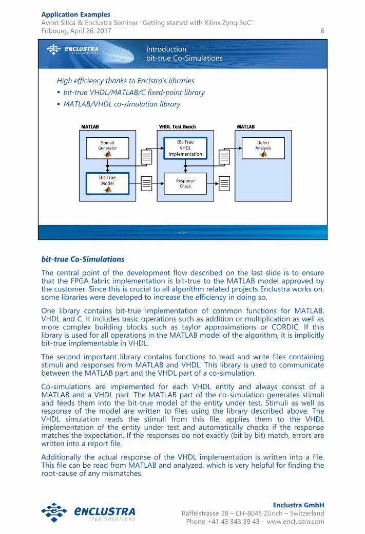
bit-true Co-Simulations
The central point of the development flow described on the last slide is to ensure that the FPGA fabric implementation is bit-true to the MATLAB model approved by the customer. Since this is crucial to all algorithm related projects Enclustra works on, some libraries were developed to increase the efficiency in doing so.
One library contains bit-true implementation of common functions for MATLAB, VHDL and C. It includes basic operations such as addition or multiplication as well as more complex building blocks such as taylor approximations or CORDIC. If this library is used for all operations in the MATLAB model of the algorithm, it is implicitly bit-true implementable in VHDL.
The second important library contains functions to read and write files containing stimuli and responses from MATLAB and VHDL. This library is used to communicate between the MATLAB part and the VHDL part of a co-simulation.
Co-simulations are implemented for each VHDL entity and always consist of a MATLAB and a VHDL part. The MATLAB part of the co-simulation generates stimuli and feeds them into the bit-true model of the entity under test. Stimuli as well as response of the model are written to files using the library described above. The VHDL simulation reads the stimuli from this file, applies them to the VHDL implementation of the entity under test and automatically checks if the response matches the expectation. If the responses do not exactly (bit by bit) match, errors are written into a report file.
Additionally the actual response of the VHDL implementation is written into a file. This file can be read from MATLAB and analyzed, which is very helpful for finding the root-cause of any mismatches.

Enclustra GmbH
Räffelstrasse 28 – CH-8045 Zürich – Switzerland
Phone +41 43 343 39 43 – www.enclustra.com
7
Application Examples
Avnet Silica & Enclustra Seminar “Getting started with Xilinx Zynq SoC”
Fribourg, April 26, 2017
Statistical Image Processing Engine
The next few slides describe the implementation of a statistical image processing
acceleration engine. The goal is not to exactly describe the engine discussed but to
pick out some interesting points.
Enclustra GmbH
Räffelstrasse 28 – CH-8045 Zürich – Switzerland
Phone +41 43 343 39 43 – www.enclustra.com
8
Application Examples
Avnet Silica & Enclustra Seminar “Getting started with Xilinx Zynq SoC”
Fribourg, April 26, 2017
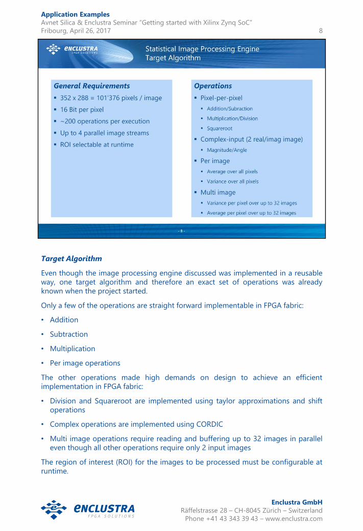
Target Algorithm
Even though the image processing engine discussed was implemented in a reusable
way, one target algorithm and therefore an exact set of operations was already
known when the project started.
Only a few of the operations are straight forward implementable in FPGA fabric:
• Addition
• Subtraction
• Multiplication
• Per image operations
The other operations made high demands on design to achieve an efficient
implementation in FPGA fabric:
• Division and Squareroot are implemented using taylor approximations and shift
operations
• Complex operations are implemented using CORDIC
• Multi image operations require reading and buffering up to 32 images in parallel
even though all other operations require only 2 input images
The region of interest (ROI) for the images to be processed must be configurable at
runtime.
Enclustra GmbH
Räffelstrasse 28 – CH-8045 Zürich – Switzerland
Phone +41 43 343 39 43 – www.enclustra.com
9
Application Examples
Avnet Silica & Enclustra Seminar “Getting started with Xilinx Zynq SoC”
Fribourg, April 26, 2017
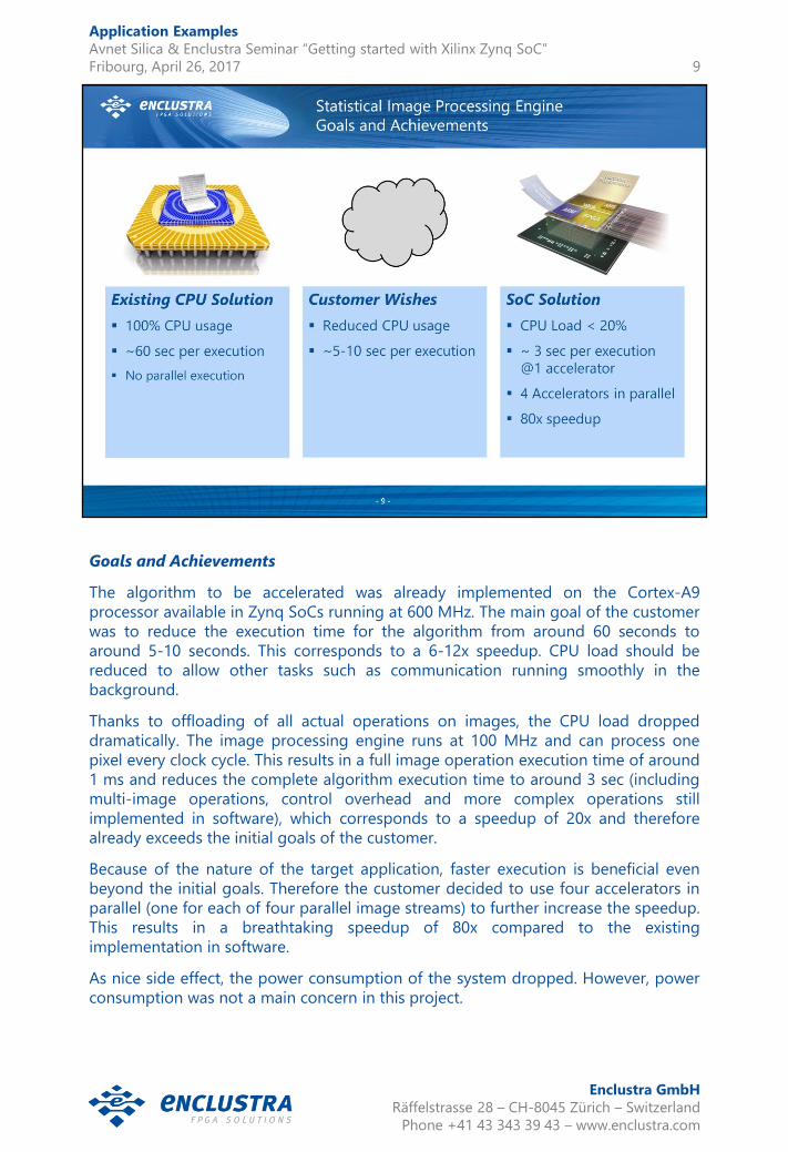
Goals and Achievements
The algorithm to be accelerated was already implemented on the Cortex-A9
processor available in Zynq SoCs running at 600 MHz. The main goal of the customer
was to reduce the execution time for the algorithm from around 60 seconds to
around 5-10 seconds. This corresponds to a 6-12x speedup. CPU load should be
reduced to allow other tasks such as communication running smoothly in the
background.
Thanks to offloading of all actual operations on images, the CPU load dropped
dramatically. The image processing engine runs at 100 MHz and can process one
pixel every clock cycle. This results in a full image operation execution time of around
1 ms and reduces the complete algorithm execution time to around 3 sec (including
multi-image operations, control overhead and more complex operations still
implemented in software), which corresponds to a speedup of 20x and therefore
already exceeds the initial goals of the customer.
Because of the nature of the target application, faster execution is beneficial even
beyond the initial goals. Therefore the customer decided to use four accelerators in
parallel (one for each of four parallel image streams) to further increase the speedup.
This results in a breathtaking speedup of 80x compared to the existing
implementation in software.
As nice side effect, the power consumption of the system dropped. However, power
consumption was not a main concern in this project.
Enclustra GmbH
Räffelstrasse 28 – CH-8045 Zürich – Switzerland
Phone +41 43 343 39 43 – www.enclustra.com
10
Application Examples
Avnet Silica & Enclustra Seminar “Getting started with Xilinx Zynq SoC”
Fribourg, April 26, 2017
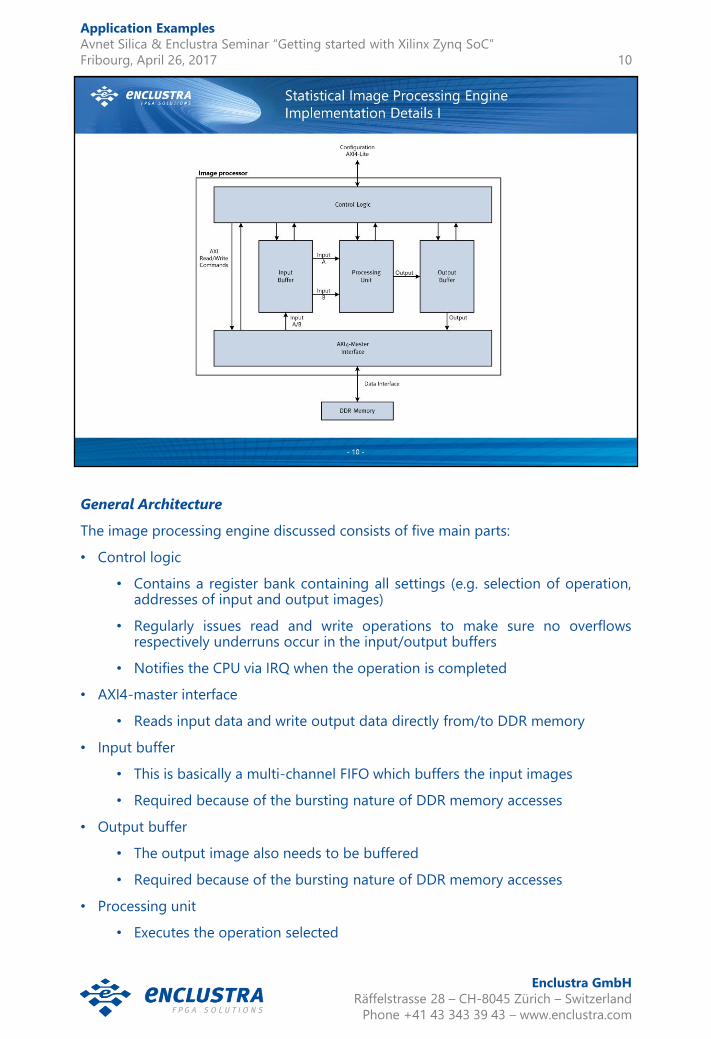
General Architecture
The image processing engine discussed consists of five main parts:
• Control logic
• Contains a register bank containing all settings (e.g. selection of operation, addresses of input and output images)
• Regularly issues read and write operations to make sure no overflows respectively underruns occur in the input/output buffers
• Notifies the CPU via IRQ when the operation is completed
• AXI4-master interface
• Reads input data and write output data directly from/to DDR memory
• Input buffer
• This is basically a multi-channel FIFO which buffers the input images
• Required because of the bursting nature of DDR memory accesses
• Output buffer
• The output image also needs to be buffered
• Required because of the bursting nature of DDR memory accesses
• Processing unit
• Executes the operation selected
Enclustra GmbH
Räffelstrasse 28 – CH-8045 Zürich – Switzerland
Phone +41 43 343 39 43 – www.enclustra.com
11
Application Examples
Avnet Silica & Enclustra Seminar “Getting started with Xilinx Zynq SoC”
Fribourg, April 26, 2017
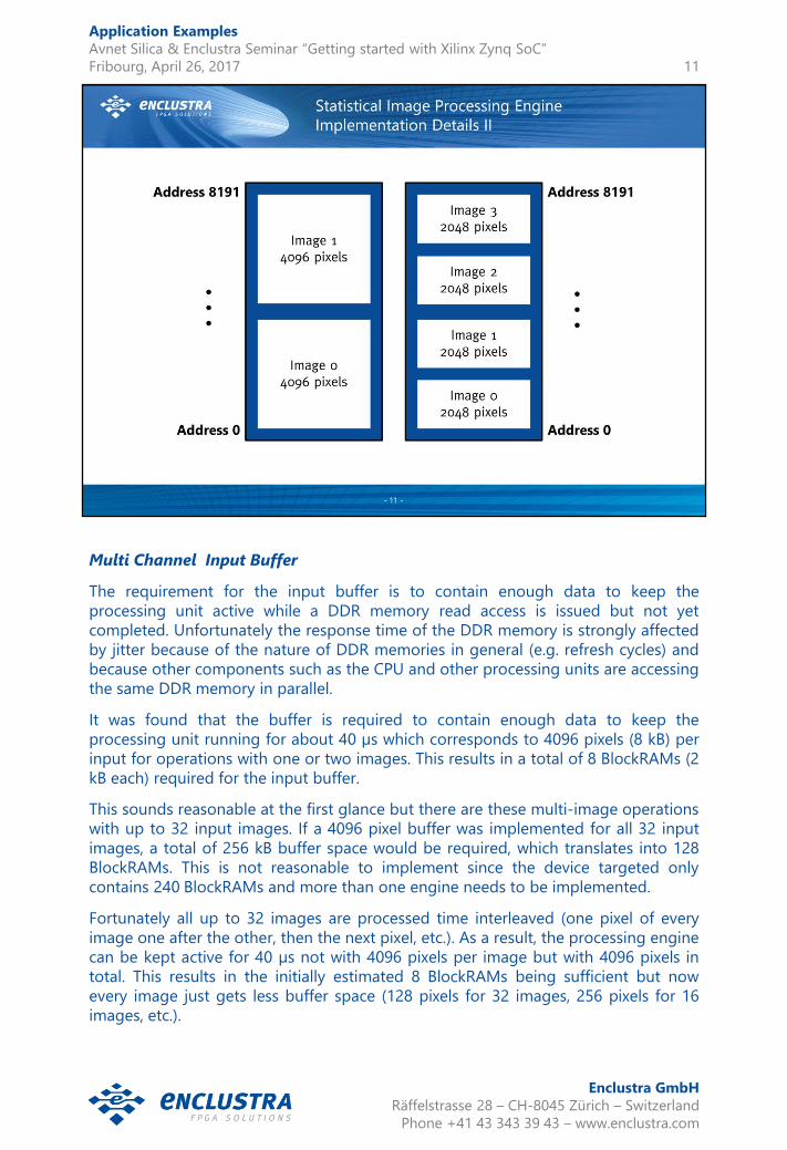
Multi Channel Input Buffer
The requirement for the input buffer is to contain enough data to keep the
processing unit active while a DDR memory read access is issued but not yet
completed. Unfortunately the response time of the DDR memory is strongly affected
by jitter because of the nature of DDR memories in general (e.g. refresh cycles) and
because other components such as the CPU and other processing units are accessing
the same DDR memory in parallel.
It was found that the buffer is required to contain enough data to keep the
processing unit running for about 40 µs which corresponds to 4096 pixels (8 kB) per
input for operations with one or two images. This results in a total of 8 BlockRAMs (2
kB each) required for the input buffer.
This sounds reasonable at the first glance but there are these multi-image operations
with up to 32 input images. If a 4096 pixel buffer was implemented for all 32 input
images, a total of 256 kB buffer space would be required, which translates into 128
BlockRAMs. This is not reasonable to implement since the device targeted only
contains 240 BlockRAMs and more than one engine needs to be implemented.
Fortunately all up to 32 images are processed time interleaved (one pixel of every
image one after the other, then the next pixel, etc.). As a result, the processing engine
can be kept active for 40 µs not with 4096 pixels per image but with 4096 pixels in
total. This results in the initially estimated 8 BlockRAMs being sufficient but now
every image just gets less buffer space (128 pixels for 32 images, 256 pixels for 16
images, etc.).
Enclustra GmbH
Räffelstrasse 28 – CH-8045 Zürich – Switzerland
Phone +41 43 343 39 43 – www.enclustra.com
12
Application Examples
Avnet Silica & Enclustra Seminar “Getting started with Xilinx Zynq SoC”
Fribourg, April 26, 2017
Division Implementation
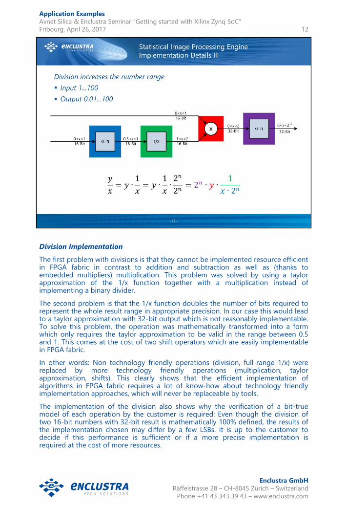
The first problem with divisions is that they cannot be implemented resource efficient in FPGA fabric in contrast to addition and subtraction as well as (thanks to embedded multipliers) multiplication. This problem was solved by using a taylor approximation of the 1/x function together with a multiplication instead of implementing a binary divider.
The second problem is that the 1/x function doubles the number of bits required to represent the whole result range in appropriate precision. In our case this would lead to a taylor approximation with 32-bit output which is not reasonably implementable. To solve this problem, the operation was mathematically transformed into a form which only requires the taylor approximation to be valid in the range between 0.5 and 1. This comes at the cost of two shift operators which are easily implementable in FPGA fabric.
In other words: Non technology friendly operations (division, full-range 1/x) were replaced by more technology friendly operations (multiplication, taylor approximation, shifts). This clearly shows that the efficient implementation of algorithms in FPGA fabric requires a lot of know-how about technology friendly implementation approaches, which will never be replaceable by tools.
The implementation of the division also shows why the verification of a bit-true model of each operation by the customer is required: Even though the division of two 16-bit numbers with 32-bit result is mathematically 100% defined, the results of the implementation chosen may differ by a few LSBs. It is up to the customer to decide if this performance is sufficient or if a more precise implementation is required at the cost of more resources.
Enclustra GmbH
Räffelstrasse 28 – CH-8045 Zürich – Switzerland
Phone +41 43 343 39 43 – www.enclustra.com
13
Application Examples
Avnet Silica & Enclustra Seminar “Getting started with Xilinx Zynq SoC”
Fribourg, April 26, 2017
Bluetooth Transceiver Engine
The next few slides describe the implementation of a Bluetooth transceiver engine.
Again the goal is not to explain each and every detail but to select some interesting
points and discuss them.
Enclustra GmbH
Räffelstrasse 28 – CH-8045 Zürich – Switzerland
Phone +41 43 343 39 43 – www.enclustra.com
14
Application Examples
Avnet Silica & Enclustra Seminar “Getting started with Xilinx Zynq SoC”
Fribourg, April 26, 2017
Requirements
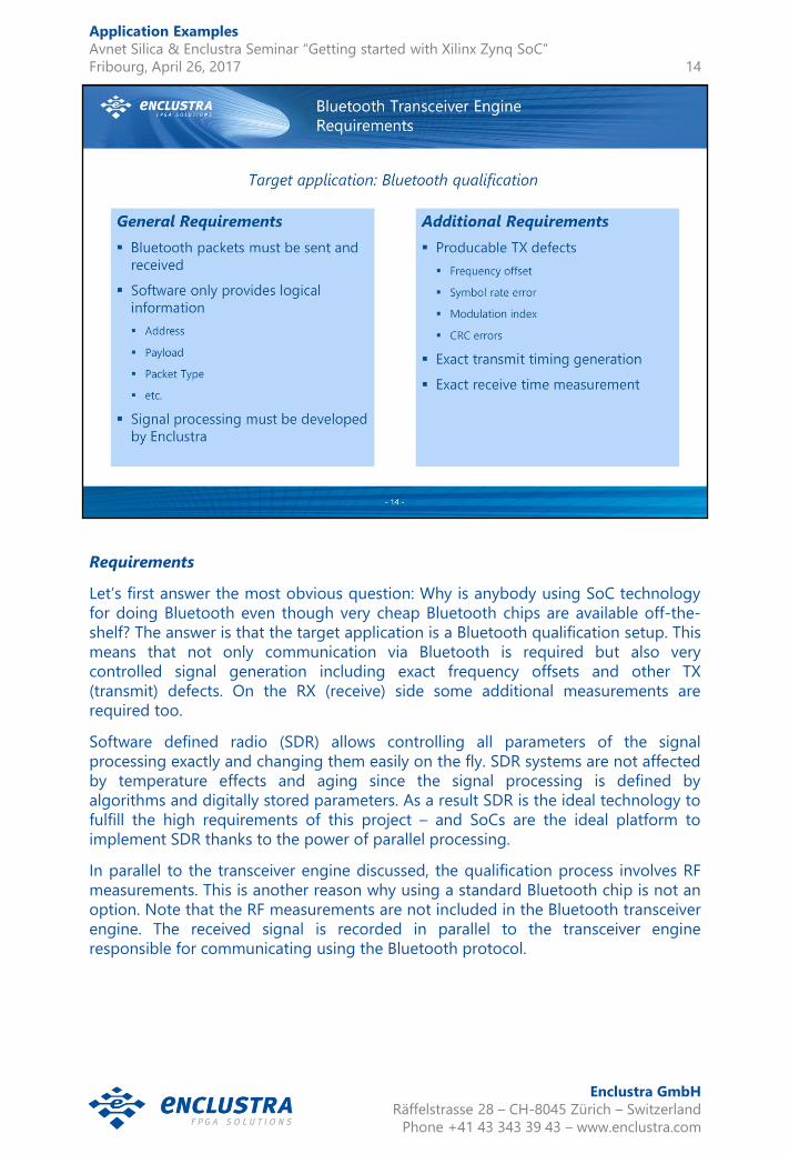
Let’s first answer the most obvious question: Why is anybody using SoC technology
for doing Bluetooth even though very cheap Bluetooth chips are available off-the-
shelf? The answer is that the target application is a Bluetooth qualification setup. This
means that not only communication via Bluetooth is required but also very
controlled signal generation including exact frequency offsets and other TX
(transmit) defects. On the RX (receive) side some additional measurements are
required too.
Software defined radio (SDR) allows controlling all parameters of the signal
processing exactly and changing them easily on the fly. SDR systems are not affected
by temperature effects and aging since the signal processing is defined by
algorithms and digitally stored parameters. As a result SDR is the ideal technology to
fulfill the high requirements of this project – and SoCs are the ideal platform to
implement SDR thanks to the power of parallel processing.
In parallel to the transceiver engine discussed, the qualification process involves RF
measurements. This is another reason why using a standard Bluetooth chip is not an
option. Note that the RF measurements are not included in the Bluetooth transceiver
engine. The received signal is recorded in parallel to the transceiver engine
responsible for communicating using the Bluetooth protocol.
Enclustra GmbH
Räffelstrasse 28 – CH-8045 Zürich – Switzerland
Phone +41 43 343 39 43 – www.enclustra.com
15
Application Examples
Avnet Silica & Enclustra Seminar “Getting started with Xilinx Zynq SoC”
Fribourg, April 26, 2017
Bluetooth Protocol Basics
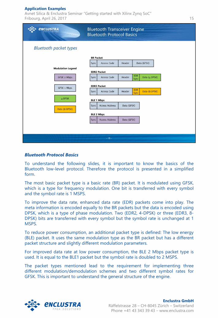
To understand the following slides, it is important to know the basics of the
Bluetooth low-level protocol. Therefore the protocol is presented in a simplified
form.
The most basic packet type is a basic rate (BR) packet. It is modulated using GFSK,
which is a type for frequency modulation. One bit is transferred with every symbol
and the symbol rate is 1 MSPS.
To improve the data rate, enhanced data rate (EDR) packets come into play. The
meta information is encoded equally to the BR packets but the data is encoded using
DPSK, which is a type of phase modulation. Two (EDR2, 4-DPSK) or three (EDR3, 8-
DPSK) bits are transferred with every symbol but the symbol rate is unchanged at 1
MSPS.
To reduce power consumption, an additional packet type is defined: The low energy
(BLE) packet. It uses the same modulation type as the BR packet but has a different
packet structure and slightly different modulation parameters.
For improved data rate at low power consumption, the BLE 2 Mbps packet type is
used. It is equal to the BLE1 packet but the symbol rate is doubled to 2 MSPS.
The packet types mentioned lead to the requirement for implementing three
different modulation/demodulation schemes and two different symbol rates for
GFSK. This is important to understand the general structure of the engine.
Enclustra GmbH
Räffelstrasse 28 – CH-8045 Zürich – Switzerland
Phone +41 43 343 39 43 – www.enclustra.com
16
Application Examples
Avnet Silica & Enclustra Seminar “Getting started with Xilinx Zynq SoC”
Fribourg, April 26, 2017
General Architecture
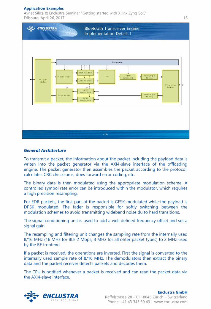
To transmit a packet, the information about the packet including the payload data is
writen into the packet generator via the AXI4-slave interface of the offloading
engine. The packet generator then assembles the packet according to the protocol,
calculates CRC checksums, does forward error coding, etc.
The binary data is then modulated using the appropriate modulation scheme. A
controlled symbol rate error can be introduced within the modulator, which requires
a high precision resampling.
For EDR packets, the first part of the packet is GFSK modulated while the payload is
DPSK modulated. The fader is responsible for softly switching between the
modulation schemes to avoid transmitting wideband noise du to hard transitions.
The signal conditioning unit is used to add a well defined frequency offset and set a
signal gain.
The resampling and filtering unit changes the sampling rate from the internally used
8/16 MHz (16 MHz for BLE 2 Mbps, 8 MHz for all ohter packet types) to 2 MHz used
by the RF frontend.
If a packet is received, the operations are inverted. First the signal is converted to the
internally used sample rate of 8/16 MHz. The demodulators then extract the binary
data and the packet receiver detects packets and decodes them.
The CPU is notified whenever a packet is received and can read the packet data via
the AXI4-slave interface.

Enclustra GmbH
Räffelstrasse 28 – CH-8045 Zürich – Switzerland
Phone +41 43 343 39 43 – www.enclustra.com
17
Application Examples
Avnet Silica & Enclustra Seminar “Getting started with Xilinx Zynq SoC”
Fribourg, April 26, 2017
Loopback Testing in Simulations and on Hardware
To achieve a good test coverage and find all issues before delivering the offloading
engine, a thorough testing concept was implemented additionally to the normal
regression testing concept in use at Enclustra (self-checking regression tests).
In simulations the whole processing chain was simulated in a loopback configuration
(blue) for only a hand full of packets due to long simulation runtimes.
Additionally several loopback paths are implemented and can be activated on
hardware. This allows testing many thousands of packets within a short time. Thanks
to multiple loopback paths (red), any problems can be roughly located very quickly
which saves a lot of debugging time. Before delivering the Bluetooth transceiver
engine to the cusomer, loopback tests for over a million packets were run including
the RF frontend and the antenna.
Thanks to the consideration of loopback tests early in the concept phase, care was
taken to design the system symmetrically (e.g. same sample rates and number
formats on RX and TX side) to ease the implementation of loopback tests. This
greatly reduced the testing effort.

Enclustra GmbH
Räffelstrasse 28 – CH-8045 Zürich – Switzerland
Phone +41 43 343 39 43 – www.enclustra.com
18
Application Examples
Avnet Silica & Enclustra Seminar “Getting started with Xilinx Zynq SoC”
Fribourg, April 26, 2017
Efficient FIR Filter Implementation using FPGA Fabric
FIR filters are one of the most cited examples for the parallel processing power of
SoCs and FPGAs. They fit the strengths of FPGA fabric very well because of its
multiply-accumulate power provided by DSP-slices.
For one given filter within the receive path of the Bluetooth transceiver engine, a 64-
tap FIR filter with a sample rate of 16 MSPS is required. In this case a fully parallel
implementation of the FIR filter is not efficient, since it would require much resources
(64 DSP slices) but run at a clock speed way below what FPGA fabric is capable of
(16 MHz). A fully serial implementation using only one DSP slice is not possible either
since this would require a clock speed of over 1 GHz which is far beyond the
possibilities of FPGA fabric.
The implementation chosen contains 8 DSP slices doing multiply accumulate
operations. It therefore requires 8 clock cycles to execute all 64 multiplications. An
additional DSP slice is used to sum up the results of all 8 clock cycles. This partially
parallel architecture allows using a small number of DSP slices (8 pieces) at a
reasonable clock speed (128 MHz) to achieve the performance required.
Considering that even the smallest Xilinx SoC device contains 80 DSP slices, this
example shows that with 10% of the DSP resources of the smallest SoC device, a filter
performance of over 1 GMAC/s is easily achievable and that this is not just a
theoretical number but proven in a real-world project.

Enclustra GmbH
Räffelstrasse 28 – CH-8045 Zürich – Switzerland
Phone +41 43 343 39 43 – www.enclustra.com
19
Application Examples
Avnet Silica & Enclustra Seminar “Getting started with Xilinx Zynq SoC”
Fribourg, April 26, 2017
Modeling Signal Processing Paths – The tv-Concept
In the project discussed, Enclustra created bit-true models of all signal processing
components and the customer could verify the performance of the algorithm
developed before implementation started.
Unfortunately many signal processing elements such as filters introduce delay and/or
change the sample rate. It is therefore difficult to track a given signal accross the
whole processing chain and compare the same parts of the signal (in terms of «the
signal related to the same symbols») at various stages of the processing.
To improve this situation, the tv-concept was used. This means a signal always
consists of a value vector (v) and a time vector (t). The time vector is changed along
with the processing. A processing delay leads to a shift on the time axis, a up- or
down-sampling leads to a interpolation or decimation of the time vector. Using this
concept, data can always be ploted related to the time vector and is aligned correctly
for analysis.
The tv-concept may seem like a purely MATLAB specific issue but it is important in
general for the development of signal processing offloading engines since it makes
models created by the «offloading engine designer» easily understandable to the
«application engineer» approving them. The communication between these two
parties is crucial for efficiency and success, exactly as communication is in gerneral
for engineering projects multiple parties work on.
Enclustra GmbH
Räffelstrasse 28 – CH-8045 Zürich – Switzerland
Phone +41 43 343 39 43 – www.enclustra.com
20
Application Examples
Avnet Silica & Enclustra Seminar “Getting started with Xilinx Zynq SoC”
Fribourg, April 26, 2017
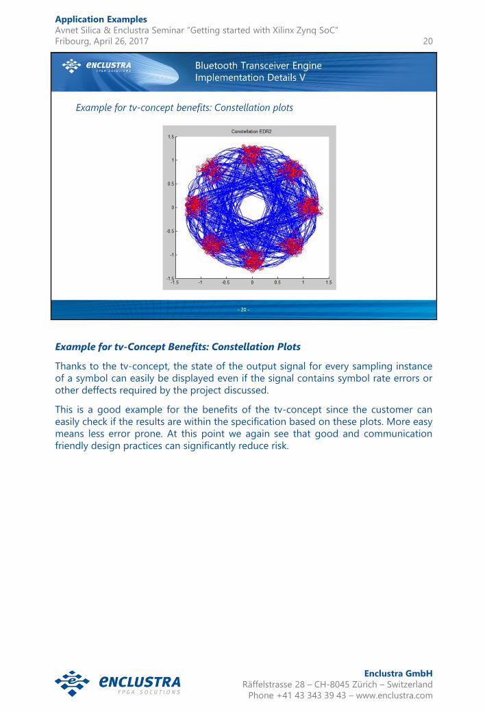
Example for tv-Concept Benefits: Constellation Plots
Thanks to the tv-concept, the state of the output signal for every sampling instance
of a symbol can easily be displayed even if the signal contains symbol rate errors or
other deffects required by the project discussed.
This is a good example for the benefits of the tv-concept since the customer can
easily check if the results are within the specification based on these plots. More easy
means less error prone. At this point we again see that good and communication
friendly design practices can significantly reduce risk.

Enclustra GmbH
Räffelstrasse 28 – CH-8045 Zürich – Switzerland
Phone +41 43 343 39 43 – www.enclustra.com
21
Application Examples
Avnet Silica & Enclustra Seminar “Getting started with Xilinx Zynq SoC”
Fribourg, April 26, 2017
Project Achievements
Thanks to the design methodology used and a thorough testing concept, there was
no need to touch the algorithm after the implementation. There were also no
significant bugs recovered after delivery. As a result of these points, the project was
delivered on schedule and without any additional effort required.
The computing power of the offloading engine is quite high with 4.5 GMAC/sec and
the CPU is available to 100% for the protocol handling and qualification flow control.

Enclustra GmbH
Räffelstrasse 28 – CH-8045 Zürich – Switzerland
Phone +41 43 343 39 43 – www.enclustra.com
22
Application Examples
Avnet Silica & Enclustra Seminar “Getting started with Xilinx Zynq SoC”
Fribourg, April 26, 2017
Enclustra GmbH
Räffelstrasse 28 – CH-8045 Zürich – Switzerland
Phone +41 43 343 39 43 – www.enclustra.com
23
Application Examples
Avnet Silica & Enclustra Seminar “Getting started with Xilinx Zynq SoC”
Fribourg, April 26, 2017
SoC Benefits
The two examples discussed illustrate the power of SoCs. Propperly designed
offloading engines can boost the system performance and at the same time reduce
the CPU load. In the statistical image processing example this led to significantly
reduced runtimes. The realization of the Bluetooht transceiver example would not
even have been possible with a CPU approach since performance requirements could
not be fullfilled.
The statistical image processing engine is a very good example for a reusable
offloading engine. The customer paid for development once but can benefit from
the results in multiple product generations.
In the case of the Bluetooth transceiver, the abstraction level of the software written
by the customer could be raised significantly. The customer does neither need to
take care of the signal processing nor of the low-level protocol encoding and
decoding. All these things are fully implemented by Enclustra in the offloading
engine.
One common point of both projects discussed is that they show that successful
outsourcing of the offloading engine development is possible.

Enclustra GmbH
Räffelstrasse 28 – CH-8045 Zürich – Switzerland
Phone +41 43 343 39 43 – www.enclustra.com
24
Application Examples
Avnet Silica & Enclustra Seminar “Getting started with Xilinx Zynq SoC”
Fribourg, April 26, 2017
No Gain wihtout Brain
An FPGA is not a CPU and it is not programmable the same way as a CPU.
Programming an FPGA means designing a chip and requires a significantly different
skillset and experience.
A good example for this is the fact that algorithms often need to be converted into a
form that is efficiently implementable in FPGA fabric. To do so, deep techology
specific know-how is required. As a result the decision to either strongly invest in
building up this know-how or to outsource it must be taken. Anything between these
two ways likely results in suboptimal results.
There are many EDA tools such as SDx from Xilinx, which help speeding up the
implementation process and significantly increase productivity. Important to
understand is the point, that these tools really only help with the implementation
and do not replace the technology specific know-how required to find an efficient
way to implement a given task in FPGA fabric.
High-level design entry tools for FPGA fabric are comparable to compilers in the
software world. They certainly can help you raising the abstraction level and getting
forward faster but most of the performance and memory footprint of any application
are given by architectural decisions. No compiler or programming language will ever
choose a good software architecture. It just implements the architecture chosen by
the engineer in an efficient way.
Enclustra GmbH
Räffelstrasse 28 – CH-8045 Zürich – Switzerland
Phone +41 43 343 39 43 – www.enclustra.com
25
Application Examples
Avnet Silica & Enclustra Seminar “Getting started with Xilinx Zynq SoC”
Fribourg, April 26, 2017
Communication Matters
During the development of the offloading engines discussed in this presentation, no
significant communication problems occured. This did not just happen but required a
lot of attention and the availability of the tools required (e.g. bit-true libraries) and
experience from earlier projects.
The problem of communication between different engieering disciplines is often
underestimated. Efficient communication requires each engineer to have a basic
knoweldge in the area the others are working in.
With SoCs, the requirement for communication has significantly increased since tasks
can be moved from fabric to the CPU and vice versa virtually seamlessly. To benefit
from this, each side needs to be able to estimate the feasibilty of solving a problem
in the other part of the SoC. As a result of this, the ideal SoC engineer should have
experience in software and FPGA development.
SoCs also increase the requirement for thorough testing. Even though each
engineering discipline (software, FPGA) is good at debugging the things it created,
much time is lost if the part created by the other discipline does not work. The only
way to avoid delays caused by this problem is to implement thorough testing
concepts on both sides before integrating the whole system.
The importance of communication is not affected by the general project setup. It
applies if software and offloading engine are developed by different companies (as
in the examples) as well as if they are developed by different teams of the same
company or even by different engineers in one team.

Enclustra GmbH
Räffelstrasse 28 – CH-8045 Zürich – Switzerland
Phone +41 43 343 39 43 – www.enclustra.com
26
Application Examples
Avnet Silica & Enclustra Seminar “Getting started with Xilinx Zynq SoC”
Fribourg, April 26, 2017

Enclustra GmbH
Räffelstrasse 28 – CH-8045 Zürich – Switzerland
Phone +41 43 343 39 43 – www.enclustra.com
27
Application Examples
Avnet Silica & Enclustra Seminar “Getting started with Xilinx Zynq SoC”
Fribourg, April 26, 2017