Embed Size (px)
Citation preview
March 2014 DocID025946 Rev 1 1/109
AN4446Application note
SPC574K72xx safety manual
IntroductionThis document is the SPC574K72xx safety manual. It provides the conditions of use for the SPC574K72xx in ISO 26262 ASIL D applications.
www.st.com
Contents AN4446
2/109 DocID025946 Rev 1
Contents
1 Preface . . . . . . . . . . . . . . . . . . . . . . . . . . . . . . . . . . . . . . . . . . . . . . . . . . . . 7
2 General Information . . . . . . . . . . . . . . . . . . . . . . . . . . . . . . . . . . . . . . . . . 9
2.1 Mission Profile . . . . . . . . . . . . . . . . . . . . . . . . . . . . . . . . . . . . . . . . . . . . . . 9
2.2 Functional safety – ISO 26262 compliance . . . . . . . . . . . . . . . . . . . . . . . . 9
2.3 Safety goals . . . . . . . . . . . . . . . . . . . . . . . . . . . . . . . . . . . . . . . . . . . . . . . 10
2.3.1 Safe state . . . . . . . . . . . . . . . . . . . . . . . . . . . . . . . . . . . . . . . . . . . . . . . . 10
2.4 Correct operation . . . . . . . . . . . . . . . . . . . . . . . . . . . . . . . . . . . . . . . . . . . .11
2.5 Failure indication signaling . . . . . . . . . . . . . . . . . . . . . . . . . . . . . . . . . . . . .11
2.6 Failure indication time . . . . . . . . . . . . . . . . . . . . . . . . . . . . . . . . . . . . . . . .11
2.6.1 Minimum failure indication time . . . . . . . . . . . . . . . . . . . . . . . . . . . . . . . 12
2.7 Failure handling . . . . . . . . . . . . . . . . . . . . . . . . . . . . . . . . . . . . . . . . . . . . 12
3 Functional safety requirements for application software . . . . . . . . . . 14
3.1 Disabled modes of operation . . . . . . . . . . . . . . . . . . . . . . . . . . . . . . . . . . 14
3.1.1 Debug mode . . . . . . . . . . . . . . . . . . . . . . . . . . . . . . . . . . . . . . . . . . . . . 14
3.1.2 Test mode . . . . . . . . . . . . . . . . . . . . . . . . . . . . . . . . . . . . . . . . . . . . . . . 14
3.2 Initial checks and configurations . . . . . . . . . . . . . . . . . . . . . . . . . . . . . . . 15
3.2.1 I/O pin/ball configuration . . . . . . . . . . . . . . . . . . . . . . . . . . . . . . . . . . . . 15
3.2.2 MCU configuration . . . . . . . . . . . . . . . . . . . . . . . . . . . . . . . . . . . . . . . . . 16
3.2.3 Mode Entry (MC_ME) . . . . . . . . . . . . . . . . . . . . . . . . . . . . . . . . . . . . . . 17
3.2.4 Start-up configuration check . . . . . . . . . . . . . . . . . . . . . . . . . . . . . . . . . 18
3.2.5 Dual core lockstep mode . . . . . . . . . . . . . . . . . . . . . . . . . . . . . . . . . . . . 18
3.2.6 FCCU fault reaction configuration . . . . . . . . . . . . . . . . . . . . . . . . . . . . . 19
3.2.7 Reset Generation Module (MC_RGM) . . . . . . . . . . . . . . . . . . . . . . . . . 20
3.2.8 Self-test completion . . . . . . . . . . . . . . . . . . . . . . . . . . . . . . . . . . . . . . . . 22
3.2.9 MEMU initial checks . . . . . . . . . . . . . . . . . . . . . . . . . . . . . . . . . . . . . . . 24
3.2.10 Flash memory configuration and tests . . . . . . . . . . . . . . . . . . . . . . . . . . 24
3.2.11 Voltage monitor configuration . . . . . . . . . . . . . . . . . . . . . . . . . . . . . . . . 25
3.2.12 Temperature monitoring configuration . . . . . . . . . . . . . . . . . . . . . . . . . . 27
3.2.13 Clock monitoring configuration . . . . . . . . . . . . . . . . . . . . . . . . . . . . . . . 27
3.2.14 System clock availability . . . . . . . . . . . . . . . . . . . . . . . . . . . . . . . . . . . . 28
3.2.15 Clock Generation Module (MC_CGM) . . . . . . . . . . . . . . . . . . . . . . . . . . 28
DocID025946 Rev 1 3/109
AN4446 Contents
4
3.2.16 FMPLL generated clocking . . . . . . . . . . . . . . . . . . . . . . . . . . . . . . . . . . 29
3.2.17 XBAR configuration . . . . . . . . . . . . . . . . . . . . . . . . . . . . . . . . . . . . . . . . 29
3.2.18 Platform flash memory controller . . . . . . . . . . . . . . . . . . . . . . . . . . . . . . 30
3.2.19 Wake-Up Unit (WKPU) / External NMI . . . . . . . . . . . . . . . . . . . . . . . . . . 30
3.2.20 Cache . . . . . . . . . . . . . . . . . . . . . . . . . . . . . . . . . . . . . . . . . . . . . . . . . . 30
3.2.21 Software Watchdog Timer (SWT) . . . . . . . . . . . . . . . . . . . . . . . . . . . . . 31
3.2.22 Analog to Digital Converters . . . . . . . . . . . . . . . . . . . . . . . . . . . . . . . . . 31
3.2.23 Temperature sensor (TSENS) . . . . . . . . . . . . . . . . . . . . . . . . . . . . . . . . 33
3.3 Runtime checks . . . . . . . . . . . . . . . . . . . . . . . . . . . . . . . . . . . . . . . . . . . . 33
3.3.1 General requirements . . . . . . . . . . . . . . . . . . . . . . . . . . . . . . . . . . . . . . 33
3.3.2 CRC of configuration registers . . . . . . . . . . . . . . . . . . . . . . . . . . . . . . . . 34
3.3.3 XBAR usage . . . . . . . . . . . . . . . . . . . . . . . . . . . . . . . . . . . . . . . . . . . . . 34
3.3.4 System Memory Protection Unit (SMPU) . . . . . . . . . . . . . . . . . . . . . . . 35
3.3.5 Platform flash memory controller . . . . . . . . . . . . . . . . . . . . . . . . . . . . . . 35
3.3.6 Flash memory . . . . . . . . . . . . . . . . . . . . . . . . . . . . . . . . . . . . . . . . . . . . 36
3.3.7 PRAMC configuration . . . . . . . . . . . . . . . . . . . . . . . . . . . . . . . . . . . . . . 38
3.3.8 RAM . . . . . . . . . . . . . . . . . . . . . . . . . . . . . . . . . . . . . . . . . . . . . . . . . . . . 38
3.3.9 ECC Bypass using core registers and Indirect Memory Access (IMA) . 40
3.3.10 Decorated Storage Memory Controller (DSMC) . . . . . . . . . . . . . . . . . . 41
3.3.11 Interrupt management . . . . . . . . . . . . . . . . . . . . . . . . . . . . . . . . . . . . . . 41
3.3.12 eDMA usage . . . . . . . . . . . . . . . . . . . . . . . . . . . . . . . . . . . . . . . . . . . . . 42
3.3.13 Reset Generation Module (MC_RGM) . . . . . . . . . . . . . . . . . . . . . . . . . 42
3.3.14 Detection of unwanted resets . . . . . . . . . . . . . . . . . . . . . . . . . . . . . . . . 42
3.3.15 Periodic Interrupt Timer (PIT) . . . . . . . . . . . . . . . . . . . . . . . . . . . . . . . . 61
3.3.16 System Timer Module (STM) usage . . . . . . . . . . . . . . . . . . . . . . . . . . . 61
3.3.17 I/O and Peripheral Bridge . . . . . . . . . . . . . . . . . . . . . . . . . . . . . . . . . . . 61
3.3.18 System Integration Unit Lite (SIUL2) . . . . . . . . . . . . . . . . . . . . . . . . . . . 63
3.3.19 GTM Wrapper . . . . . . . . . . . . . . . . . . . . . . . . . . . . . . . . . . . . . . . . . . . . 64
3.3.20 External Bus Interface (EBI) . . . . . . . . . . . . . . . . . . . . . . . . . . . . . . . . . 64
3.3.21 Reading analog inputs . . . . . . . . . . . . . . . . . . . . . . . . . . . . . . . . . . . . . . 64
3.3.22 Software Watchdog Timer (SWT) usage . . . . . . . . . . . . . . . . . . . . . . . . 64
3.3.23 Communication peripherals . . . . . . . . . . . . . . . . . . . . . . . . . . . . . . . . . . 65
3.3.24 Temperature sensor (TSENS) . . . . . . . . . . . . . . . . . . . . . . . . . . . . . . . . 65
3.3.25 Analog to Digital Converters . . . . . . . . . . . . . . . . . . . . . . . . . . . . . . . . . 66
3.3.26 Mode Entry (MC_ME) . . . . . . . . . . . . . . . . . . . . . . . . . . . . . . . . . . . . . . 67
3.3.27 Semaphores (SEMA42) . . . . . . . . . . . . . . . . . . . . . . . . . . . . . . . . . . . . . 68
3.4 Operational interference protection . . . . . . . . . . . . . . . . . . . . . . . . . . . . . 68
Contents AN4446
4/109 DocID025946 Rev 1
3.4.1 Core Memory Protection Unit (CMPU) . . . . . . . . . . . . . . . . . . . . . . . . . 68
3.4.2 System Memory Protection Unit (SMPU) . . . . . . . . . . . . . . . . . . . . . . . 69
3.4.3 AIPS protection mechanism . . . . . . . . . . . . . . . . . . . . . . . . . . . . . . . . . 69
3.4.4 Register protection (REG_PROT) . . . . . . . . . . . . . . . . . . . . . . . . . . . . . 69
3.4.5 Peripheral Core (Core_2) . . . . . . . . . . . . . . . . . . . . . . . . . . . . . . . . . . . 70
4 Functions of external devices for ASIL D applications . . . . . . . . . . . . 71
4.1 External reset output . . . . . . . . . . . . . . . . . . . . . . . . . . . . . . . . . . . . . . . . 71
4.2 High impedance outputs . . . . . . . . . . . . . . . . . . . . . . . . . . . . . . . . . . . . . . 71
4.3 External Watchdog (EXWD) . . . . . . . . . . . . . . . . . . . . . . . . . . . . . . . . . . . 71
4.4 Power supply . . . . . . . . . . . . . . . . . . . . . . . . . . . . . . . . . . . . . . . . . . . . . . 72
4.5 Error Out Monitor (ERRM) . . . . . . . . . . . . . . . . . . . . . . . . . . . . . . . . . . . . 73
4.5.1 Both FCCU pins connected to external device . . . . . . . . . . . . . . . . . . . 73
4.5.2 Single FCCU pin connected to external device . . . . . . . . . . . . . . . . . . . 74
5 Address decoding coverage . . . . . . . . . . . . . . . . . . . . . . . . . . . . . . . . . 75
5.1 Overview . . . . . . . . . . . . . . . . . . . . . . . . . . . . . . . . . . . . . . . . . . . . . . . . . 75
5.2 Test implementation . . . . . . . . . . . . . . . . . . . . . . . . . . . . . . . . . . . . . . . . . 75
5.3 How to obtain the list of locations to be read . . . . . . . . . . . . . . . . . . . . . . 81
5.3.1 Memories including block address decoding . . . . . . . . . . . . . . . . . . . . . 89
5.4 Test result . . . . . . . . . . . . . . . . . . . . . . . . . . . . . . . . . . . . . . . . . . . . . . . . . 93
5.4.1 Multiple single bit error in the same word-line . . . . . . . . . . . . . . . . . . . . 94
6 Testing All-X in RAM . . . . . . . . . . . . . . . . . . . . . . . . . . . . . . . . . . . . . . . . 95
6.1 Candidate address for testing All-X issue . . . . . . . . . . . . . . . . . . . . . . . . 95
6.2 ECC checkbit/syndrome coding scheme . . . . . . . . . . . . . . . . . . . . . . . . 100
Appendix A Further information . . . . . . . . . . . . . . . . . . . . . . . . . . . . . . . . . . . . . 106
A.1 Conventions and terminology . . . . . . . . . . . . . . . . . . . . . . . . . . . . . . . . . 106
A.2 Acronyms and abbreviations . . . . . . . . . . . . . . . . . . . . . . . . . . . . . . . . . . 106
Document revision history. . . . . . . . . . . . . . . . . . . . . . . . . . . . . . . . . . . . . . . . . . . 108
DocID025946 Rev 1 5/109
AN4446 List of tables
5
List of tables
Table 1. Temperature Profile for Packaged Device . . . . . . . . . . . . . . . . . . . . . . . . . . . . . . . . . . . . . . 9Table 2. Effects of reset . . . . . . . . . . . . . . . . . . . . . . . . . . . . . . . . . . . . . . . . . . . . . . . . . . . . . . . . . . 44Table 3. SPC574K72xx required external monitors . . . . . . . . . . . . . . . . . . . . . . . . . . . . . . . . . . . . . 72Table 4. FCCU EOUT pin behavior . . . . . . . . . . . . . . . . . . . . . . . . . . . . . . . . . . . . . . . . . . . . . . . . . 73Table 5. List of RAMs for self-test. . . . . . . . . . . . . . . . . . . . . . . . . . . . . . . . . . . . . . . . . . . . . . . . . . . 76Table 6. Example of back-to-back read to implement the test . . . . . . . . . . . . . . . . . . . . . . . . . . . . . 81Table 7. Victim address and its complementary . . . . . . . . . . . . . . . . . . . . . . . . . . . . . . . . . . . . . . . . 82Table 8. All combinations of DecA are considered . . . . . . . . . . . . . . . . . . . . . . . . . . . . . . . . . . . . . . 82Table 9. All combinations of DecB are considered . . . . . . . . . . . . . . . . . . . . . . . . . . . . . . . . . . . . . . 83Table 10. All combinations of DecC and DecD are considered . . . . . . . . . . . . . . . . . . . . . . . . . . . . . 84Table 11. All cells should be read; to decrease the testing time the algorithm is optimized. . . . . . . . 85Table 12. First step to reduce the number of cells to be read . . . . . . . . . . . . . . . . . . . . . . . . . . . . . . 86Table 13. In grey the locations to be read by the self-test . . . . . . . . . . . . . . . . . . . . . . . . . . . . . . . . . 87Table 14. First 4 cells to be read . . . . . . . . . . . . . . . . . . . . . . . . . . . . . . . . . . . . . . . . . . . . . . . . . . . . 88Table 15. Final list of locations which shall be read including the order . . . . . . . . . . . . . . . . . . . . . . . 89Table 16. List of locations to be read on block 0b001 . . . . . . . . . . . . . . . . . . . . . . . . . . . . . . . . . . . . 90Table 17. Reads related to the complementary block . . . . . . . . . . . . . . . . . . . . . . . . . . . . . . . . . . . . 91Table 18. Reading on same word-line, but different blocks . . . . . . . . . . . . . . . . . . . . . . . . . . . . . . . . 92Table 19. Final list of locations which shall be read including the order in case of memory with block
decoding . . . . . . . . . . . . . . . . . . . . . . . . . . . . . . . . . . . . . . . . . . . . . . . . . . . . . . . . . . . . . . . 93Table 20. Additional cells shall be read in case of multiple single bit in the same word-line . . . . . . . 94Table 21. E2E ECC basic H-matrix definition . . . . . . . . . . . . . . . . . . . . . . . . . . . . . . . . . . . . . . . . . . 101Table 22. List of conventions and terminology . . . . . . . . . . . . . . . . . . . . . . . . . . . . . . . . . . . . . . . . . 106Table 23. Acronyms and abbreviations . . . . . . . . . . . . . . . . . . . . . . . . . . . . . . . . . . . . . . . . . . . . . . 106Table 24. Document revision history . . . . . . . . . . . . . . . . . . . . . . . . . . . . . . . . . . . . . . . . . . . . . . . . 108
List of figures AN4446
6/109 DocID025946 Rev 1
List of figures
Figure 1. Example of QFP176 pin/pad adjacency . . . . . . . . . . . . . . . . . . . . . . . . . . . . . . . . . . . . . . . 16Figure 2. Block scheme of the SAR ADCs, including the supervisor ADC . . . . . . . . . . . . . . . . . . . . 32Figure 3. SPC574K72xx peripheral allocation . . . . . . . . . . . . . . . . . . . . . . . . . . . . . . . . . . . . . . . . . . 62Figure 4. Bit grouping of the victim address considering the SRAM . . . . . . . . . . . . . . . . . . . . . . . . . 81Figure 5. Bit grouping of the victim address considering the D-Mem. . . . . . . . . . . . . . . . . . . . . . . . . 89Figure 6. C Language encodeECC function description . . . . . . . . . . . . . . . . . . . . . . . . . . . . . . . . . 102
DocID025946 Rev 1 7/109
AN4446 Preface
108
1 Preface
Assumption: This document provides guidelines for the proper use of the SPC574K72xx Microcontroller Unit (MCU) in ASIL D applications. It will help guide the user with the steps necessary to integrate the SPC574K72xx into their application.
Assumption: The SPC574K72xx will be used as a component within a safety related application. To allow an analysis of the MCU's capability to reach the required safety level, assumptions have been made (following the concept of SEooC described in the ISO26262). These assumptions are on the scope of the MCU (for example, including external components interacting with the MCU) and on its usage by application software. The FMEDA provided with the SPC574K72xx was conducted under inclusion of these assumptions.
Assumption: A typical safety function operates by reading input from the SPC574K72xx's I/O facilities (including network connections), processing this input possibly using, generating, and storing results valid for several calculation cycles, and sending output to other system components (for example, actuators or other MCUs) again using the SPC574K72xx's I/O facilities.
This document considers:
• The system assembly that contains the SPC574K72xx MCU
• The “Safety Element out of Context” section in the “Road vehicles - Functional safety - Part 10: Guideline [ISO/DIS 26262-10]” standard
• Certain assumptions about the assembly's functional safety needs based on that standard and determines whether a measure is an assumption or not based on these factors.
What this means for designers using the SPC574K72xx is that if they don’t fulfill a specific Safety Manual (SM) assumption they have to show that their alternative solution is similarly efficient concerning the safety requirement in question (for example, provides the same coverage, avoids Common Cause Failure (CCF) as effectively, and so on), show that the particular issue is irrelevant for their application (for example, the module is not used), or estimate how much the failure rate increases and the failure metrics (SPFM/LFM) decrease due to the deviation. Otherwise, the FMEDA provided with the SPC574K72xx is not valid.
This document also contains guidelines on how to configure and operate the SPC574K72xx for ASIL D applications. These guidelines are preceded by one of the following bold text statements:
• Implementation hint
• Recommendation
Note: Further information about safety configuration and operation can be found in the SPC574K72xx Reference Manual’s “Functional Safety” chapter.
These guidelines are considered to be useful approaches for the specific topics under discussion, but are not mandatory. The user will need to use discretion in deciding whether these measures are appropriate for their applications.
This document is only valid under the assumption that:
• Assumption:he SPC574K72xx is used in automotive applications for use cases requiring a fail-silent or a fail-indicate MCU.
• The environmental conditions given in the SPC574K72xx Data Sheet are maintained.
Preface AN4446
8/109 DocID025946 Rev 1
As for all devices, device errata must be taken into account during system design and implementation. For a safety-related device such as the SPC574K72xx, this also concerns safety-related activities such as system safety concept development. The FMEDA and Safety Concept are valid if the listed assumptions in the text are covered.
Assumption: All relevant hardware safety mechanisms are enabled and configured correctly when using any of the information in this document.
General failure rate, or even an FMEDA (Failure Modes, Effects & Diagnostic Analysis) report, is available upon request when covered by a STMicroelectronics NDA (contact your STMicroelectronics representative).
DocID025946 Rev 1 9/109
AN4446 General Information
108
2 General Information
2.1 Mission ProfileLifetime for a SPC574K72xx is 20 years which is equivalent to 20000 hours of active operation for the MCU. The assumed mission profile is:
• Lifetime: 20 years
• Total operating hours: 20000 hours
• Assumption: Trip time (driving cycle): 12 hours
– This is the maximum time of operation of the SPC574K72xx without a start-up reset.
• Assumption: Fault-Tolerant Time Interval (FTTI, also known as Process Safety Time, PST) = 10 ms
– FTTI is the time the controlled system will not transition to a hazardous state, despite the SPC574K72xx failing.
Note: This is a conservative estimate since the actual number depends on MCU application (See Section 2.6: Failure indication time, for exact calculation instructions).
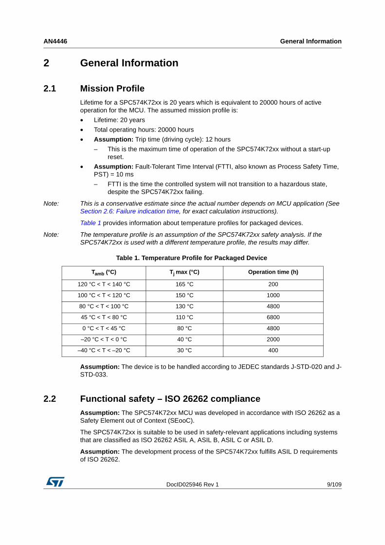
Table 1 provides information about temperature profiles for packaged devices.
Note: The temperature profile is an assumption of the SPC574K72xx safety analysis. If the SPC574K72xx is used with a different temperature profile, the results may differ.
Assumption: The device is to be handled according to JEDEC standards J-STD-020 and J-STD-033.
2.2 Functional safety – ISO 26262 complianceAssumption: The SPC574K72xx MCU was developed in accordance with ISO 26262 as a Safety Element out of Context (SEooC).
The SPC574K72xx is suitable to be used in safety-relevant applications including systems that are classified as ISO 26262 ASIL A, ASIL B, ASIL C or ASIL D.
Assumption: The development process of the SPC574K72xx fulfills ASIL D requirements of ISO 26262.
Table 1. Temperature Profile for Packaged Device
Tamb (°C) Tj max (°C) Operation time (h)
120 °C < T < 140 °C 165 °C 200
100 °C < T < 120 °C 150 °C 1000
80 °C < T < 100 °C 130 °C 4800
45 °C < T < 80 °C 110 °C 6800
0 °C < T < 45 °C 80 °C 4800
–20 °C < T < 0 °C 40 °C 2000
–40 °C < T < –20 °C 30 °C 400
General Information AN4446
10/109 DocID025946 Rev 1
2.3 Safety goalsThe safety goals of the MCU are defined as follows:
• The primary safety goal is that the SPC574K72xx does not leave its safe states for intervals equal or longer than the FTTI (10 ms) unless configured by the application software to do so.
• The secondary safety goal is that the SPC574K72xx, or the software running on the SPC574K72xx, shall be able to detect the permanent unavailability of any safety mechanism that is necessary to achieve the primary safety goal, and this shall be done at least once per driving cycle (12 hrs.).
The ASIL for the first goal is D, for the second it is B.
2.3.1 Safe state
A Safe state of the system is named Safe statesystem whereas the Safe state of the MPC5746M is named Safe stateMCU. A Safe statesystem of a system is an operating mode without an unreasonable probability of occurrence of physical injury or damage to the health of persons.
Assumption: The safety goals are achieved by transitioning or holding the SPC574K72xx in the following Safe stateMCU:
• Assumption: Completely unpowered
• Assumption: In reset
• Assumption: Operating correctly (See Section 2.4: Correct operation)
• Assumption: Explicitly indicating an internal error
If the SPC574K72xx continuously switches between a standard operating state and the reset state, without any device shutdown, the MCU is not considered to be in a Safe stateMCU (See Section 3.2.7: Reset Generation Module (MC_RGM) for details).
Assumption: The application shall identify and signal such switching as a failure condition.
If the SPC574K72xx signals an internal failure via its error out signals (FI[0], FI[1]), the surrounding subsystem should no longer use the SPC574K72xx outputs for safety functions since these signals are no longer considered reliable. This means that if an error is indicated, the system must be able to remain in a Safe statesystem without any additional actions by the MCU. Depending on its configuration, the system may disable or reset the MCU as a reaction to the error signal.
Assumption: It is assumed that the system reacts safely to the SPC574K72xx being in or entering all safe states shown in Section 2.3.1: Safe state.
DocID025946 Rev 1 11/109
AN4446 General Information
108
2.4 Correct operationAssumption: Correct operation of the SPC574K72xx is defined as:
• Assumption: Vital system modules (ViMos) and other supporting modules (SuMos) are operating according to specification.
• Assumption: Peripheral modules (PeMos) are operating according to specification.
• Assumption: Non-safety modules (NoSaMos) are not interfering with the operation of other modules.
• Other support modules (SuMo) are safety-relevant and in principle potential members of the ViMos category, and cannot lead to a violation of the safety goal on their own. Typically, these will only have multiple point faults, but not single point faults.
Note: See “Module classification” table in the SPC574K72xx Reference Manual’s “Functional Safety” chapter for specific module safety classification.
2.5 Failure indication signalingThe Fault Collection and Control Unit (FCCU) offers a hardware channel to collect errors and to bring the device to a Safe stateMCU when a failure is present in the device. The FCCU provides two error output pins (FI[0] and FI[1], on PB[11] and PC[2], respectively) as a failure indication to the external world.
Different protocols for the error output pins are supported:
• Dual rail protocol
• Time switching protocol
• Bi-stable protocol
If bi-stable protocol is selected, it is possible to use only one of the two error output pins on the SPC574K72xx. Since the pin multiplexing that is utilized for each of the error output signals works differently, FI[0] should be the signal used in this configuration.
After start-up reset, the error output signal FI[0] is in high impedance while FI[1] is functionally a GPIO input with a weak pullup. An error status flag can be read to verify if the FCCU is in an error state. The flag can be written by software to either 1 to indicate fault or 0 to indicate operational state. The error output pins transition to the operational state only on software request.
A functional reset has no influence on FI[0] but sets FI[1] to high impedance with a pullup. To avoid changing FI[1] during functional reset when time switching or bi-stable protocol is used, it is recommended to write 0 to FCCU_CFG[PS].
Refer to Section 4.5: Error Out Monitor (ERRM) for details on specific requirements for connecting FI[0] and FI[1] to an external device.
2.6 Failure indication timeFailure indication time is the time it takes from the occurrence of a failure to when the indication of that failure is visible by driving the error out pins or by assertion of reset.
The failure indication time of the SPC574K72xx is finite. It must be taken into account when determining application safety strategies since failure indication time plus reaction time on this indication by the system must be less than the FTTI.
General Information AN4446
12/109 DocID025946 Rev 1
Failure indication time has three components, two of which are influenced by certain configuration choices: Failure indication time = recognition time + internal processing time + indication time.
Each component of failure indication time is briefly described as follows:
• Recognition time is the maximum of the recognition time of all involved safety mechanisms. The two mechanisms with the longest times are:
– Recognition time related to the FMPLL loss of clock: This time depends on the FMPLL configuration. This time is approximately 20 µs.
– Diagnostic cycle time of software self-tests. This time depends closely on the software implemented.
• Internal processing time lasts a maximum 10 IRCOSC clock cycles (nominal frequency of IRCOSC is 16 MHz).
• Indication time is the time to notify an observer about the failure. This time depends on the indication protocol in the FCCU:
– Dual Rail protocol and time switching protocol –
FCCU configured as “fast switching mode”: indication delay is maximum 64 µs. As soon as the FCCU receives a fault signal, it reports the failure to the outside world via an output pin (if properly configured).
FCCU configured as “slow switching mode”: an indication delay could occur. The maximum delay is equal to the period of the error out signal, which toggles at a frequency of 61 Hz.
– Bi-stable protocol: indication delay is maximum 64 µs. As soon as the FCCU receives a fault signal, the FCCU reports the failure via an output pin (if properly configured).
If the configured reaction to a fault is an interrupt, an additional delay (interrupt latency) can occur until the interrupt handler is able to start executing (for example, higher priority IRQs, XBAR contention, register saving, and so on).
Assumption: The overall failure indication time shall be less than the FTTI of the application (assumed FTTI shown in Section 2.1: Mission Profile).
2.6.1 Minimum failure indication time
When a failure event occurs, one or both error output signals (Fn) are set to show an error condition for a minimum time (T_min), even if software attempts to reset the state of the error out signals. The external failure indication stays in failure mode for a configurable minimum time as shown in Equation 1. For bi-stable protocol the time DELTA_T is configurable by software up to a maximum of 10 ms by configuring FCCU_DELTA_T[DELTA_T].
Equation 1 T_min = 250 μs + FCCU_DELTA_T[DELTA_T] μs
In case another failure event happens within T_min after the first failure event, the timer measuring T_min is restarted.
2.7 Failure handlingThe FCCU is responsible for reacting to internal failures. A different reaction can be configured for each failure source.
DocID025946 Rev 1 13/109
AN4446 General Information
108
Failure sources include:
• All failure indication signals from the modules within the MCU
• Control logic and signals monitored by the FCCU itself
• Software-initiated failure indications
• External failure input (via FI[0] pin)
The different failure sources, as represented by the FCCU failure inputs, are shown in “FCCU failure inputs” table in the “Functional Safety” chapter of the SPC574K72xx Reference Manual.
Available failure reactions include:
• Maskable interrupt
• Non-maskable interrupt
• Reset
• Change the state of the failure indication pin(s)
• No reaction
Additionally, the transmission capabilities of the communication controllers can be disabled when the FCCU transitions to the error state (see “Disabling of communication controllers” in the “Functional Safety” chapter of the SPC574K72xx Reference Manual).
Software can read the failure source that caused a fault from the FCCU_RF_S[0:3] registers and can do so either before or after a functional reset. Software can also reset the failure by resetting the respective status bit, but the external failure indication will stay in failure mode for a configurable amount of time (see Equation 1). When the source of the failure is determined, software can decide the next step to be taken to handle the error. The software then may decide to do nothing, cause resets of certain modules, reset the whole MCU or change the value of the error out pins (see “FCCU failure inputs” table in the SPC574K72xx Reference Manual’s “Functional Safety” chapter for error source channel numbers).
Error handling can be split into two categories:
• Handling of errors during runtime
• Handling of errors during boot-time (for example, LBIST, MBIST)
Assumption: Runtime errors shall be handled in a time shorter than the FTTI.
Assumption: Boot-time failure handling shall be handled before the safety function starts execution. Typically, the reaction is to not let the safety function start and give a failure indication to the user.
Functional safety requirements for application software AN4446
14/109 DocID025946 Rev 1
3 Functional safety requirements for application software
This section gives an overview of the necessary or recommended measures when using the individual components of SPC574K72xx. If a module in SPC574K72xx is used without following the required actions, there is a risk that the safety certificate for the entire MCU, or other modules if the failure interferes with their operation, may be invalidated.
It is possible to ignore the required measures if equivalent measures to manage the same failures are alternatively included.
Modules not explicitly covered by this document do not require any safety specific software measures.
To assist continuous product improvement, it is recommended to report field failures which occur despite following these measures to STMicroelectronics in accordance with ISO 26262-7 Chapter 6.4.2.1.
3.1 Disabled modes of operationThe system and application software must ensure that the functions described in this section are not activated while running safety-relevant operations.
3.1.1 Debug mode
The debugging facilities of the SPC574K72xx are a potential source of failure when activated during the operation of safety-relevant applications. They can halt the cores, cause breakpoint hits, write to core registers and the address space, and activate boundary scan. The MCU must therefore not enter debug mode to avoid interference with the normal operation of the application software.
The state of the JCOMP pin determines whether the system is being debugged or whether the system operates in normal operating mode. When the JCOMP pin is logic low, the JTAGC TAP controller is kept in reset for normal operating mode. When it is logic high, the JTAGC TAP controller is enabled to enter debug mode. The system must ensure that it does not attempt to enable debug mode by externally asserting the JCOMP pin during boot up. Otherwise, a fault condition signal will be sent to the FCCU.
Assumption: Debugging will be disabled in the field while the device is being used for safety-relevant functions.
Assumption: For normal operation software needs to configure the Software Watchdog Timer (SWT), clock generation, and FCCU to continue execution in debug mode (to not ‘freeze’ operation when in debug mode) (for example, SWT_CR[FRZ] = 0).
3.1.2 Test mode
Several mechanisms of the SPC574K72xx can be circumvented in test mode, undermining the safety concept. Test mode is used for comprehensive factory testing and should not be used in normal operating mode.
The TEST pin is for testing purposes only and should be tied to GND in normal operating mode. The system must ensure the TEST pin is not asserted during boot to enable test
DocID025946 Rev 1 15/109
AN4446 Functional safety requirements for application software
108
mode. The activation of test mode is supervised by the FCCU and will signal a fault condition when test mode is entered.
Assumption: Test mode will be disabled in the field while the device is being used for safety-relevant functions.
To avoid unwanted activation of the testing circuitry the Design For Testability (DFTn) FCCU error inputs must be enabled even if they are not needed by the application. The FCCU channels for DFT[1:4] are 46 to 49, respectively. These error inputs are enabled by setting the appropriate bits in the following registers:
• FCCU_RF_CFG
• FCCU_RFS_CFG
• FCCU_RF_TOE
• FCCU_RF_E
• FCCU_IRQ_ALARM_EN
• FCCU_NMI_EN
• FCCU_EOUT_SIG_EN
3.2 Initial checks and configurationsAfter start-up, the application software must ensure the conditions described in this section are satisfied before safety-relevant functions are enabled. Additional configuration is needed to ensure freedom from interference between cores and between concurrent software (see Section 3.4: Operational interference protection).
3.2.1 I/O pin/ball configuration
Assumption: The user shall avoid configurations that place redundant signals on neighboring pads or pins.
Hether two functions on two package pins/balls are adjacent to each other, refer to the mechanical drawings of the packages (see the SPC574K72xx Data Sheet) together with the pin/spheres (balls) number information of the packages as seen in the SPC574K72xx Reference Manuals “System Integration Unit Lite2 (SIUL2)” section and the table “Signal descriptions and output / input multiplexing assignment table”.
The internal die pad sequence can be derived from the package pin sequence of the 176 LQFP-EP pin package shown in the SPC574K72xx Data Sheet.
Functional safety requirements for application software AN4446
16/109 DocID025946 Rev 1
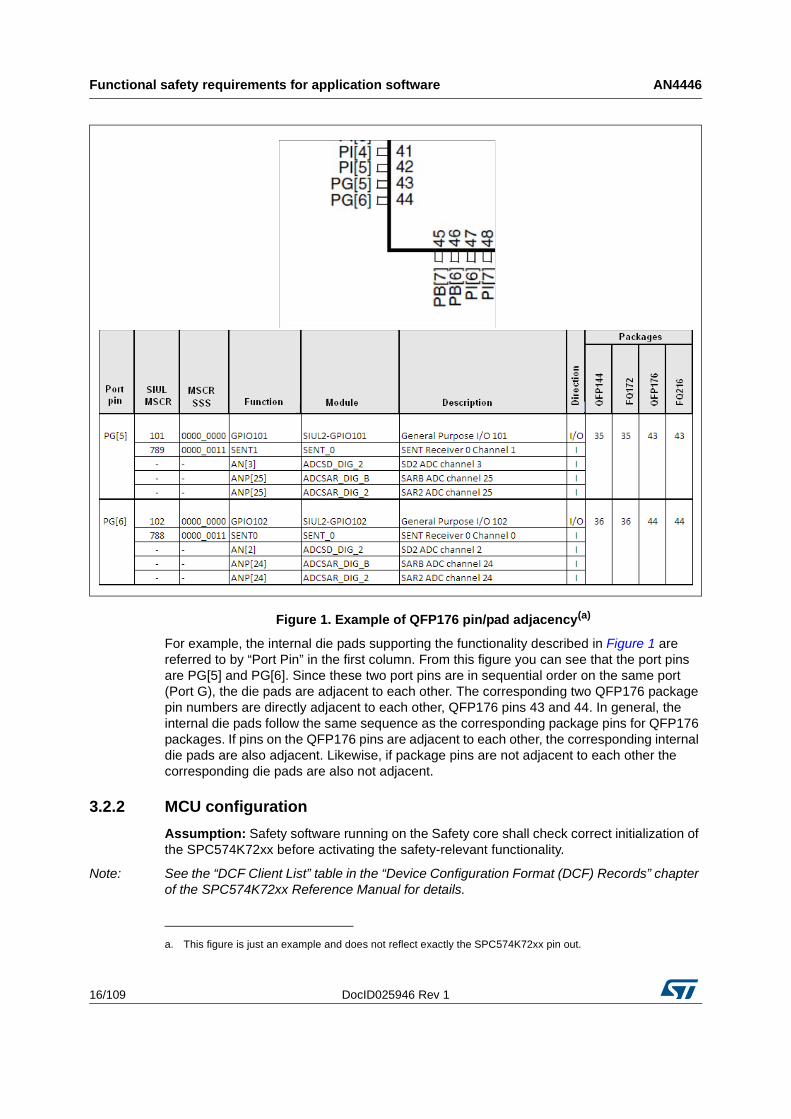
Figure 1. Example of QFP176 pin/pad adjacency(a)
For example, the internal die pads supporting the functionality described in Figure 1 are referred to by “Port Pin” in the first column. From this figure you can see that the port pins are PG[5] and PG[6]. Since these two port pins are in sequential order on the same port (Port G), the die pads are adjacent to each other. The corresponding two QFP176 package pin numbers are directly adjacent to each other, QFP176 pins 43 and 44. In general, the internal die pads follow the same sequence as the corresponding package pins for QFP176 packages. If pins on the QFP176 pins are adjacent to each other, the corresponding internal die pads are also adjacent. Likewise, if package pins are not adjacent to each other the corresponding die pads are also not adjacent.
3.2.2 MCU configuration
Assumption: Safety software running on the Safety core shall check correct initialization of the SPC574K72xx before activating the safety-relevant functionality.
Note: See the “DCF Client List” table in the “Device Configuration Format (DCF) Records” chapter of the SPC574K72xx Reference Manual for details.
a. This figure is just an example and does not reflect exactly the SPC574K72xx pin out.
DocID025946 Rev 1 17/109
AN4446 Functional safety requirements for application software
108
Note: See the “The IOP executes code to apply device setting” section in the “Reset and Boot” chapter of the SPC574K72xx Reference Manual for details on the IOP phase of the boot
Assumption: FMEDA assumes that the device is properly configured by the DCF records in the TEST sector of the flash memory to enable the Hardware Security Module (HSM) I/O Processor (Core 2) handshaking during the boot phase.
Note: See the “Reset sequence flow based on initial device condition” section of the “Reset and boot” chapter of the SPC574K72xx Reference Manual for details.
The MCU memory configuration and the JTAG Part ID number can be read in the SSCM_MEMCONFIG register (JTAG Part ID = SSCM_MEMCONFIG[JPIN]).
This information is normally used for debugging purposes, and is not necessary for the safety function.
Assumption: Application software does not use the JTAG Part ID, nor does it affect safety critical operations.
With the System Status and Configuration Module (SSCM) it is possible to configure different MCU behaviors (for example, determine primary boot vector, abort disable/enable).
Assumption: SSCM shall be configured to trigger an exception in case of any access to a peripheral slot not used on the device (SSCM_ERROR register).
Assumption: Once after the boot application shall perform an intended access to an unimplemented memory space and check for the expected abort to occur.
The FCCU can be configured to trigger a NMI to the Safety core if a fault is detected. In the case of a functional reset, this NMI is masked by hardware and is unmasked during BAF execution. The NMI service routine is executed as soon as the safety core is activated.
In the worst case, this flow can cause an unwanted functional reset loop. For example, assume a situation which can not be recovered by software, and the NMI service routine can only trigger a functional reset. After the reset, the BAF unmasks the NMI which triggers the Safety core. Which cause the NMI to execute again.
Assumption: Pending FCCU faults shall be cleared before enabling the Safety core after a functional reset.
From an application standpoint this means:
1. Do not activate the Safety core automatically during or after the BAF.
2. Initialize the FCCU (may be preceded by a software reset of the FCCU).
3. Activate the Safety core.
3.2.3 Mode Entry (MC_ME)
To overcome faults in the wakeup and interrupt inputs to the MC_ME, the following is assumed if the application uses Low Power mode (LP):
• Assumption: The duration in LP mode is monitored. If the system does not wake up within a specified time frame, the system will be reset by the monitor (for example, SWT can provide the time monitoring).
• Assumption: Software will perform a test of entry and exit to and from LP mode at startup.
Functional safety requirements for application software AN4446
18/109 DocID025946 Rev 1
An incorrect clock source as the system clock could be selected due to faults, resulting in multiple faults. In order to improve detection of such faults, and the effect by the clock monitors:
• Assumption: It is assumed that the nominal frequency of different clock sources that are available as the system clock have different frequencies.
The mode configuration registers of MC_ME take effect only when the mode transition request is initiated. Thus, instead of the configuration registers the global status register should be CRCed (if configuration register CRCing is done) as that represents the current state.
Assumption: Application software shall check the target mode configuration immediately before issuing a mode transition request.
Assumption: In order to check that a mode transition has been correctly executed, after initiating a mode transition request, software shall verify the mode transition status within the expected completion delay. Also, the new configuration is compared with the intended configuration. This does not apply if the target mode transition is to LP mode.
Note: The MC_ME implements a register to request a mode transition and registers that report the status of the transition (for example, ME_GS, ME_IMTS, ME_DMTS registers).
The monitoring and types of reactions can be enabled in the FCCU for the following fault inputs(b):
• Compensation disable (FCCU ch 53)
• SAFE mode (FCCU ch 54)
3.2.4 Start-up configuration check
During boot, start-up software is not executed on the safety core.
Assumption: Safety software running on the safety core shall check correct initialization of the SPC574K72xx before activating the safety-relevant functionality. This check shall not be executed on the core executing the start-up software.
3.2.5 Dual core lockstep mode
The SPC574K72xx device operates in delayed lockstep mode (LSM) to allow the highest safety level to be reached. The checker core will receive all inputs delayed by two clock cycles. Outputs of the checker core will be compared with outputs of the master core. Any differences will be flagged as an error which will be processed by the FCCU.
For safety operation the appropriate configuration in the flash memory must not be programmed to disable LSM. If the LSM is disabled, the checker core and the Redundancy Checker Control Units (RCCUs) are disabled. This triggers a fault indication to the FCCU. The checker core will not work independently from the master core. No dynamic switching is possible between LSM on and LSM off (any change to the respective bit in Flash will only take effect after the next reset).
Before starting safety-relevant operations, the application software shall check that lockstep mode is enabled (confirm MC_ME_CS[S_CORE1] = 1 (checker) and
b. See the “Module classification” table in the SPC574K72xx Reference Manual’s “Functional Safety” chapter for specific module safety classification.
DocID025946 Rev 1 19/109
AN4446 Functional safety requirements for application software
108
MC_ME_CS[S_CORE2] = 1 (master), confirm that no failure is signalled on alarm #51, for example) and configure the FCCU to react to lockstep disablement.
Assumption: Before starting safety-relevant operations, the application software shall check that lockstep mode is enabled (for example, confirm MC_ME_CS[S_CORE1] = 1 (core_0, master) and MC_ME_CS[S_CORE2] = 1 (core_0s, checker), and no failure is signalled on FCCU fault 51 (Lockstep mode)), then configure the FCCU to react to lockstep disablement.
3.2.6 FCCU fault reaction configuration
The Fault Collection and Control Unit (FCCU) collects faults and manages the reaction to these faults. A mechanism is usually provided to allow software to check the integrity of the different error paths. Most reactions are disabled at boot time so software configuration is required. Refer to Section 2.7: Failure handling for the valid FCCU fault reactions.
Assumption: Application software shall check the FCCU configuration once after programming.
The FCCU is checked by the FCCU Output Supervision Unit (FOSU) which provides a secondary path for the failure indication and reports to the Reset Generation Module (MC_RGM). The FOSU only causes a reset if the FCCU fails to react to an enabled incoming enabled fault within a fixed time interval (1000 IRCOSC cycles). The FOSU does not require software configuration. While the FCCU is in its CONFIG state, the FOSU does not monitor the FCCU for faults or the resulting reaction.
Assumption: Application software shall check and clear any pending faults when it moves the FCCU out of the CONFIG state.
Assumption: Before starting safety-relevant operations, software must configure the fault reactions to each fault that is safety-relevant for the application.
Note: Implementation hint: Software must program the FCCU configuration registers (for example, FCCU_RFS_CFGn, FCCU_NMI_ENn, FCCU_EOUT_SIG_ENn) to configure the fault reaction of each fault. These registers are writable only if the FCCU is in the CONFIG state.
Assumption: The integrity of the entire error reaction path shall be verified at least once after the boot.
Note: Different approaches to verify the functionality of the error reaction paths can be used. Some error reaction paths are checked during LBIST and don’t require the development of additional software, whereas others require application software.
Note: The table “FCCU failure inputs” from in the “Functional Safety” chapter of the SPC574K72xx Reference Manual shows the suggested approach for each FCCU failure input.
The FCCU will come out of reset with most of the failure inputs disabled. Failures which occur during boot will, for the most part, not be acknowledged by the FCCU as a failure. To check whether such errors have occurred, SW can read the FCCU failure status registers for any latched error and act on the status of those bits accordingly (FCCU_RF_S[0:3]).
Note: The SPC574K72xx Reference Manual’s “FCCU failure inputs” table in the “Functional Safety” chapter lists failure sources, associated FCCU channels and how they can be tested.
The error indication on pins, FI[0] and FI[1], are controlled by the SIUL2 and FCCU. The field SIUL2_MSCR[SMC] can be configured to have the output buffer disabled when the
Functional safety requirements for application software AN4446
20/109 DocID025946 Rev 1
SPC574K72xx enters Safe mode (for example, for FI[0], SIUL2_MSCR27[SMC] = 0, and for FI[1], SIUL2_MSCR34[SMC] = 0). The FCCU_CFG register is used to configure other FI[n] options like signal polarity, switching mode, software control, and so on.
Assumption: It is assumed that whenever error indication is enabled on FI[n], the SMC bit in associated MSCR register are always programmed to 1 with register access protection enabled.
The FCCU together with the INTC, can lead to cyclic reset. For example consider the following situation:
1. Error indication arrives at FCCU
2. FCCU triggers IRQ
3. SW analyzes fault and causes a reset
4. MCU comes out of reset and hands over to SW
5. SW configures INTC
6. SW gets the same IRQ again (because FCCU still holds the IRQ line), analyzes fault and causes a reset ad infinitum (or rather till the reset escalator engages and causes a destructive reset).
To avoid this situation the following assumption is considered.
Assumption: It is assumed that FCCU pending fault status should be cleared before the INTC is configured.
Since the NMI is edge triggered, even if it is kept active during a functional reset until the fault status is cleared, it will not interrupt the safety core and the described cyclic reset can't be seen.
Assumption: If the clock driving the FCCU (IRCOSC) fails, software must find other ways to signal an error other than using the FCCU control of the error output pin(s) (FI[n]).
Note: There are different methodologies that could be used to satisfy this assumption. For example, issuing a reset, or switching FI[n] pin control to a GPIO and using it to drive an error signal instead of using FI[n].
Assumption: If the FCCU uses NMI as a failure reaction, the safety core will not be enabled after a reset during the first mode transition of the MC_ME module but earliest at the second transition which will initiated earliest several IRCOSC cycles after the first.
Unwanted activation of LBIST/MBIST causes a violation of the safety goal.
Assumption: Software shall always enable FCCU reactions to error events indicating unexpected STCU2 activations.
3.2.7 Reset Generation Module (MC_RGM)
The MC_RGM is the central point for resetting the MCU. One of its tasks is to prevent reset cycling caused by reset escalation. It also can transition to SAFE mode. The SAFE mode has not been considered a Safe stateMCU during safety analysis.
Permanent cycling through otherwise safe states or permanent cycling between a safe state and an unsafe state is considered a violation of the safety goal. Specifically, this scenario relates to a continuous Reset – Start, Operation – Reset or Reset – Self-test – Reset sequence. Allowing such cycles would be problematic as it would allow an unlimited number of attempts of the test that is causing the cycle which could possibly endanger its ability to detect device failures.
DocID025946 Rev 1 21/109
AN4446 Functional safety requirements for application software
108
To detect a loop of continuous functional resets, the SPC574K72xx supports functional reset escalation which can be used to generate a destructive reset if the number of functional resets reaches the programmed value. Once the functional reset escalation is enabled, the Reset Generation Module (MC_RGM) increments a counter for each functional reset that occurs. When the number of functional resets reaches the programmed value in the MC_RGM_FRET, the MC_RGM initiates a destructive reset. The counter can be cleared by software, destructive reset or start-up reset.
A similar mechanism to detect a loop of continuous destructive resets is implemented in the MC_RGM. When the destructive reset counter reaches the programmed value, the MCU will be held in reset until the next power-on reset. The destructive reset counter can be cleared by software or by a power-on reset.
Assumption: Safety software will reset the functional and destructive reset counters every time it has finished checking its environment (for example, before making the Fn pin active). The MC_RGM_FRET (functional reset counter) and MC_RGM_DRET (destructive reset counter) registers allow the user to select the number of functional and destructive resets that can occur before action is taken (see “Reset Generation Module (MC_RGM)” in the SPC574K72xx Reference Manual for details).
Assumption: Software shall enable functional reset escalation for the condition when multiple functional resets occur consecutively.
Note: Functional reset escalation is enabled by writing a non-zero value to the MC_RGM_FRET register (see the SPC574K72xx Reference Manual’s ‘Reset Generation Module (MC_RGM)).
Reset escalation is a hardware mechanism that provides protection against a loop of continuous resets. The time between these loops can be so short that the application software doesn’t have time to take any action to manage them. Longer reset cycles must be managed by application software.
Assumption: Before clearing the reset counters of the escalation mechanism, the safety software shall ensure that longer reset cycles can be detected by the software.
Note: There are various methods to implement this requirement. For example, safety software, before clearing the reset counters, reads (and saves) the FCCU error status indication (if any faults were found) and compares the status with previous saved versions. If too many resets due to faults are observed, software can react by triggering a destructive reset.
For some events, the MC_RGM can be configured to react not with a functional reset, but with a transition to the SAFE mode (see the description of the MC_RGM_FEAR in the SPC574K72xx Reference Manual). In such a case, one watchdog shall be kept enabled. If this watchdog times out, the FCCU shall move the MCU into one of its safe states.
Assumption: If the MC_RGM is configured to react with a transition into SAFE mode, at least one watchdog timer shall remain enabled. The FCCU shall be configured to react to a timeout of this watchdog with a long functional reset or driving the error out signals to a fault condition.
Assumption: Software will read the reset status after boot ensuring that the reset cause is indicated. Then software will clear the register, and read back the value verifying that it is actually cleared.
Assumption: Resets during normal operation will be executed only as a reaction to an error, not as a functional measure. This avoids undetected faults due to interrupts that are not being generated.
Functional safety requirements for application software AN4446
22/109 DocID025946 Rev 1
3.2.8 Self-test completion
To ensure absence of latent faults, the self-test executes both a Logic Built-In Self-Test (LBIST) and a Memory Built-In Self-Test (MBIST) during boot while the device is still under reset (offline). The boot time BIST includes the scan-based LBIST to test the digital logic and the MBIST to test all RAMs and ROMs(c).
Note: The overall control of LBISTs and MBISTs is provided by the Self-Test Control Unit (STCU2). The STCU2 will execute automatically after a power-on reset(d) (POR), external reset and destructive reset, and will also execute when initiated by software (online self-test). The SPC574K72xx logic is grouped into ten LBIST partitions used for both production testing and self-test.
Note: The SPC574K72xx Reference Manual’s “Self-Test Control Unit (STCU2)” chapter and “Use cases and limitations” section discusses details on how to correctly execute offline and online self-tests.
Note: The section “Online Logical BIST (LBIST)” of the SPC574K72xx Reference Manual’s “Functional safety chapter” shows tables of the module groupings of each LBIST partition.
Assumption: If there is an LBIST failure, or MBIST detects uncorrectable failures, the STCU2 will cause a destructive reset, causing execution of the self-test again. This is to ensure that a self-test, which fails only due to a transient error, will not block device usage. If several self-tests fail in a row, the desctructive reset escalation will activate and hold the MCU in reset.
On the other hand, if MBIST detects correctable failures, software must decide whether to continue or halt execution. In fact, the MBIST may detect and report two (or more) Single Bit Errors (SBEs) occurring in multiple test passes instead of one Multiple Bit Error (MBE).
Assumption: Software will determine if two or more errors reported by the MBIST as SBEs combine to create an uncorrectable error by examining the entries in the System RAM Memory Management Unit (MEMU) instance. If several entries exist for the same address with different bit numbers, this data word actually has an MBE instead of the several SBEs discovered by the MBIST.
Assumption: After start up (and more in general, always after the execution of MBISTs), software will cross check MBIST status in the STCU2 (pass or fail) with the content of MEMU MBIST buffer (same as system RAM) to detect failures affecting the reporting of MBIST errors. This can be due to faults affecting the reporting path for MEMU or STCU2 logic. (notice that STCU2 is not part of any LBIST partition and only a pass/fail flag is available).
Assumption: After start-up and before the safety application starts, application software shall confirm that all LBISTs and MBISTs finished successfully, MISRs contain the expected values, and no critical failure is flagged. The critical failures may include LBIST failures, MBIST MBEs, MBIST SBEs exceeding the maximum tolerated number (<= 8 due to MEMU buffer size) and self-test failures.
Note: See the “Off-Line Self-Test Sequence” section in the SPC574K72xx Reference Manual for details about test sequencing and completion validation.
c. This does not include flash memory.
d. The customer must enable the self-test in the shadow sector of the flash memory since the factory default configuration will be to not run the self-test).
DocID025946 Rev 1 23/109
AN4446 Functional safety requirements for application software
108
The STCU2, as well as LBIST and MBIST controllers, are themselves subject to failures, which may prevent self-tests from executing correctly (for example, no self-test execution, or execution of the wrong algorithm). For latent faults affecting LBIST execution, checking the MISR register upon LBIST completion is considered sufficient. For MBIST only a pass/fail flag is provided (besides the collection of detected MBIST errors in the MEMU).
The following must be followed to improve the detection of latent faults, particularly those affecting correct MBIST execution:
• Recommendation: LBIST should be scheduled before MBIST since LBISTs also cover the logic running memory self-tests and the MEMU BIST error collection logic/buffers; this will help to detect latent faults responsible for the wrong or incomplete execution of memory self tests or wrong reporting of their results.
• Recommendation: The STCU2 CRC feature should be enabled to check that the signals exchanged between the STCU2 and MBIST/LBIST controllers are correct (for example, STCU2 commands and LBIST/MBIST responses).
Note: The expected signature depends on the sequence of tests. Customers can determine the expected signature by running the desired sequence of tests and reading the resulting CRC upon test completion. One signature must be computed for each test sequence (for example, one for the start-up test sequence and one for each on-line test performed).
As far as the STCU2 error reaction path is concerned, the following are given:
• Assumption: SW will check the integrity of the STCU2 Unrecoverable Fault/Recoverable Fault (UF/RF) error lines that signal the FCCU and the MC_RGM (UF only) via the fake error injection register interface provided by STCU2. Before running the test, FCCU and MC_RGM shall be configured in order not to cause undesired reaction.
• Recommendation: During the execution of the safety function, and when no on-line self-test is requested, software should disable the FCCU and MC_RGM reactions to STCU2 UF/RF error indications to avoid false trip to the safe state or interference in case of unexpected error indications.
The STCU2 provides a key-based mechanism to prevent unauthorized write accesses to its register interface. The integrity of such protection mechanism can be checked by running the following test:
• Assumption: SW shall perform a write access to one of the STCU2 registers without providing the requested key pair and check for the generation of the expected transfer error.
The STCU2 allows execution of logic and memory BIST also during runtime upon a SW request. If the I/O (including FI[n]) pins need a defined state during on-line LBIST, the following is recommended:
• Reset SIUL prior to on-line LBIST (SIUL_RST in MC_RGM).
• Set pins to a desired state (if the reset-state does not meet requirements).
The following Assumptions have to be satisfied when the on-line BIST feature is used:
• SW shall verify that STCU2 configuration is correct before triggering the execution of on-line BISTs.
• STCU2 status has to be checked after the execution of on-line LBIST/MBIST to verify that all scheduled tests have been executed and completed successfully.
• Software shall supervise the execution time of on-line self tests using the SWT or any other available timer. The internal STCU2 WDT might suffer from CCFs causing either
Functional safety requirements for application software AN4446
24/109 DocID025946 Rev 1
no, or slower, test execution. This may mean that no WDT timeout occurs (as internal WDT and STCU2 core logic share the same clock).
Note: During start-up, no safety function is executed and the start up time is supervised by the external WDT. The internal prescaler feeding both the STCU2 WDT and core logic can be checked by running an on-line test and checking its execution time.
• On completion of the on-line LBIST software shall check whether reset was correctly applied to the partition(s) under test. This can be done by checking one or more registers (at least 2 recommended) for their expected reset value. Testing is not necessary if a global system reset is applied at the end of the test.
• On exiting from a functional reset, software will check the status of the STCU2 to verify there are no running BISTs nor any hardware aborted tests.
Note: BISTs still running after a functional reset are the result of incorrectly handled hardware abort requests by the STCU2 that occurred while on-line BISTs were executing.
• If STCU2 interrupt capabilities are used to notify end of test session execution, application will handle the case of missing interrupt(s) (for example, by supervising test execution time or periodically polling STCU2 status (checking STCU2_RUNSW[RUNSW], or STCU2_INT_FLG[MBIFLG] (for MBIST) and STCU2_INT_FLG[LBIFLG] (for LBIST)).
3.2.9 MEMU initial checks
MBISTs report detected faults to the same MEMU reporting block used for System RAM ECC failures. Errors are in general distinguished between single-bit and multi-bit. However, it is not guaranteed that single-bit errors found in different steps on the same address are reported as multi-bit errors
Recommendation: The application software can write known error addresses into the MEMU reporting table to prevent reporting of those errors to the FCCU in case the addresses are accessed again.
3.2.10 Flash memory configuration and tests
SPC574K72xx provides 2,5 MB of programmable non-volatile (NVM) flash memory with ECC which can be used for instruction and/or data storage.
Assumption: To detect failures where a wrong or multiple selection targets a different block while programming, application SW shall configure flash memory blocks as read only when not the target of a write operation.
Note: See the “Program” subsection under “Modify mode” section in the “Embedded Flash Memory” chapter of the SPC574K72xx Reference Manual for details.
The flash memory array integrity self check detects possible latent faults affecting the flash memory array, including potential data retention issues, or the logic involved in read operations (for example, sense amplifiers, column mux’s, address decoder, voltage/timing references). It calculates a MISR signature over the array content and thus validates the content of the array as well as the decoder logic. The calculated MISR value is dependent on the array content and must be validated by software.
The array integrity MISR value is calculated after ECC detection and correction. Flash memory ECC logic corrects for SBEs that occur during an array integrity check (AI) if a single bit error array integrity check gives a positive result.
DocID025946 Rev 1 25/109
AN4446 Functional safety requirements for application software
108
Single bit correction reporting still occurs in the FLASH_MCR[SBC] bit and the FLASH_ADR during AI if FLASH_UT0[SBCE] = 1.
The AI breakpoint feature allows to break the Array Integrity Check execution if an error event is a single bit correction. Array Integrity Check can be resumed by the application after verifying the source of the error and clearing the respective status bit (for example, MCR[SBC] or MCR[EER]).
Assumption: The application software shall run the flash memory AI at start-up to detect possible latent faults.
Note: See the “Array Integrity Self Check” section in the SPC574K72xx Reference Manual for details.
In the event of a user detected single-bit correction through user reads or an array integrity check, a margin read may be done to check for a possible second bit failing within the selected margin levels.
Margin reads are completed at voltages that differ than the normal read voltage and life expectancy of the flash memory bitcells are impacted by the execution of margin reads. Doing margin reads repetitively results in deterioration of the flash memory array, and shorten expected life when compared to normal read levels.
Assumption: A margin read test should be executed after a new single-bit error correction has occurred in flash memory. The margin read test does not need immediate execution, but it needs to be run within the next few trip cycles. Multiple single-bit errors can be the first indications of a data retention problem that could have the potential of causing multi-bit errors. The MEMU can be used to store the address of the location reporting the error event.
Note: Implementation hint: Refer to the SPC574K72xx Reference Manual’s Margin Read” subsection in “User Test Mode” section of the “Embedded Flash Memory (c55fmc)” chapter for details.
3.2.11 Voltage monitor configuration
To assist in maintaining functional safety, the Power Management Controller (PMC) monitors various supply voltages of the SPC574K72xx device. The “POR and voltage monitors description” table in the “Power management” chapter of the SPC574K72xx Reference Manual shows a detailed list of the LVDs and HVDs embedded in the SPC574K72xx.
Apart from the self-test, the use of the PMC for ASIL D applications is transparent to the user because the operation of the PMC is automatic (see SM_FMEDA_037 below,).
The PMC LBISTs automatically execute during start-up, but the LVDs and HVDs are disabled until after the testing has completed.
PMC failures primarily report to the MC_RGM. Since safety-relevant voltages have the potential to disable the failure indication mechanisms of the SPC574K72xx (the FCCU and its error out signals), their error indication directly causes a transition into a Safe stateMCU by reset. Additionally, LVDs and HVDs also report errors to the FCCU, but under the recommended configuration (MCU reset by MC_RGM enabled) this is irrelevant.
Assumption: Software shall not disable the direct transition into a safe state due to an overvoltage or undervoltage indication.
The customer can, at their own risk, disable the direct triggering of resets by the MC_RGM and rely on the FCCU reactions to overvoltage and undervoltage, even when FCCU is
Functional safety requirements for application software AN4446
26/109 DocID025946 Rev 1
configured for IRQs as the reaction. In general, the FCCU reaction (clocked by the IRCOSC) will take more time than the MC_RGM reaction (asynchronous). So, if the FCCU is to trigger an IRQ reaction, there is an increased probability that a fast voltage drop could cause a brownout condition on the device before a reaction occurs. If IRQs are selected as the FCCU reaction, there will be no guarantee that Diagnostic Coverage of overvoltage or undervoltage will be properly detected, and the safety analysis (FMEDA) of the MCU, will not be valid with respect to this failure mode.
To check the LVDs and HVDs for latent faults, which could impact their ability to correctly trigger when an undervoltage or overvoltage situation occurs, it is assumed there will be two software self-tests that will be executed by during startup.
To check the LVDs and HVDs for latent fault which could influence their correct triggering in under-/overvoltage situations, the 2 tests are assumed to be executed by software during startup.
Assumption: Reference voltages, and input voltages of LVDs/HVDs, shall be acquired using the ADC. The conversion values shall be compared with the expected ADC values. The application software shall initiate the hardware assisted self-test to detect LVD/HVD failures after start-up.
Note: This is to check that the voltage supervised by the LVD/HVD is actually the correct one and not influenced by opens or shorts in such a way that it never could cross the LVD/HVD threshold. The LVDs/HVDs are monitored by ‘SARADC_B input channels’ 96 to 101, 104, and 112 to 118, except 115 (see the SPC574K72xx Reference Manual’s “Analog-to-Digital Converters (ADC) Configuration” chapter and the “SARADC_B analog test channel assignment” table for details).
Assumption: Software shall initiate a self-test of LVD/HVD comparator.
Note: This is to check that a LVD/HVD will trigger at approximately correct value (see the SPC574K72xx Reference Manual’s “Power Management Controller digital interface (PMC_dig)” chapter section “Voltage Detect User Mode Test Register (VD_UTST)”).
Assumption: Software shall initiate a self-test of the LVD/HVD comparator.
To run the LVD/HVD self-test, application software shall execute the following steps:
1. Mask LVD/HVD by clearing the Reset Event Enable Register (PMC_REE_TD, PMC_REE_VDn registers) of the PMC (see chapter “Power Management Controller digital interface (PMC_dig)” in the SPC574K72xx Reference Manual’s).
2. Write the PMC_VD_UTST register to start testing.
3. Verify test results by polling the Event Pending Registers (PMC_EPR_VDn or PMC_EPR_TD) flag:
a) If the flag(s) are set, LVD (or HVD) test passed as expected.
b) If the flag is not set, self-test failed.
Note: Software may configure a timeout period to be sure the flag(s) asserts within a specified time (this time shall be greater than 20 μs).
DocID025946 Rev 1 27/109
AN4446 Functional safety requirements for application software
108
1. Clear PMC_VD_UTST.
2. Enter a loop that checks the LVD (or HVD) flag in the Event Pending Register (PMC_EPR_TD or PMC_EPR_VDn), and clears the flag (writing 1 to the flag to clear).
a) If the flag is not clear, repeat the loop.
b) Once the flag clears, exit the loop.
3. Enable the LVD (or HVD) by setting the appropriate field in the Reset Event Enable Register (PMC_REE_TD or PMC_REE_VDn).
These steps shall be repeated for each LVD (or HVD) to be tested (see section “Voltage Detect User Mode Test Register (VD_UTST)” in the SPC574K72xx Reference Manual’s “Power Management Controller digital interface (PMC_dig)” chapter).
3.2.12 Temperature monitoring configuration
The SPC574K72xx supports a temperature sensor to detect over-temperature conditions. The temperature sensor can be configured to signal over-temperature faults digitally to the FCCU. It can also provide an analog measurement of the temperature using SARB input channel 120.
To set a proper threshold the customer must consider the maximum operating junction temperature (see the SPC574K72xx Data Sheet for the temperature sensor accuracy and maximum junction temperatures).
Assumption: Application software shall configure the FCCU to react to over-temperature faults indicated by the temperature sensor.
3.2.13 Clock monitoring configuration
Clocks are supervised by the Clock Monitoring Units (CMUs). The CMUs are driven by the 16 MHz internal reference clock oscillator (IRCOSC) to ensure independence from the monitored clocks. The CMUs flag errors associated with conditions due to clocks being out of programmable bounds, and loss of reference clock. If a supervised clock leaves the specified range for the device, an error signal is sent to the FCCU. SPC574K72xx includes the CMUs as shown in the “Clocking” chapter of the SPC574K72xx Reference Manual. It is the responsibility of the software to verify that the IRCOSC and XOSC are valid before starting the CMUs.
Assumption: The CMU frequency thresholds shall be configured for high and low limits which are used to compare with the MCU operating frequency.
Assumption: The potential exactness (or the required inexactness) of the CMU thresholds shall be taken into account for both the IRCOSC and clock, or clocks, being monitored.
Note: Implementation hint: For example, for the upper threshold customer should target CLKnominal_freq + CLKacc% and convert it into the number of IRC cycles in the worst case (slowest possible IRCOSC), for example IRC_freq = IRCnominal_freq – IRCacc%. The opposite applies to the lower threshold.
Assumption: For ASIL D applications, the use of the CMUs is mandatory. If the related modules are used by the application safety function, the user shall verify that the CMUs are not disabled and their faults are managed by the FCCU. The FCCU’s default configuration does not manage the CMU faults, so it shall be configured accordingly.
Assumption: Application software shall check the configuration of the CMU once after programming.
Functional safety requirements for application software AN4446
28/109 DocID025946 Rev 1
Assumption: Once after the boot the application shall measure the CLKMT0_RMN frequency (IRCOSC) with CLKMN0_RMT (XOSC) as reference clock exploiting the CMU frequency measurement feature. To detect failure of the IRCOSC, the application software shall utilize the CMU’s frequency meter to read the IRCOSC frequency and compare it against the expected value of 16 MHz(e)
Assumption: After start-up, the CMU reaction path shall be tested by modifying the CMU threshold.
Assumption: To detect delays in clock mode switching and lost clock switching, the software shall ensure the CMU is reprogrammed with the new expected clock frequency minimum and maximum values within the FTTI.
Note: The frequency range of the CMU must be increased before switching clock modes. The requirement is to program the CMU with the correct minimum and maximum values for the new frequency soon after the switch.
Recommendation: The application may run the IOSC_A001_SW (on page 28) once per FTTI to verify proper IRCOSC operation.
3.2.14 System clock availability
At start-up, the CMUs are not initialized and the IRCOSC is the default system clock. Stuck-at faults on the external oscillator (XOSC) are not detected by the CMUs at start-up since the monitoring units are not initialized and the SPC574K72xx is still running on the IRCOSC.
Assumption: The software shall verify that the clocks are valid by checking the state of the following:
1. MC_ME_GS[S_XOSC] = 1, verifies valid XOSC
2. MC_ME_GS[S_IRC] = 1, verifies valid IRCOSC
3. The quality of the IRCOSC frequency is determined by clock metering and measuring the IRCOSC against the XOSC (see the SPC574K72xx Reference Manual’s “Clock Monitoring Unit (CMU)” chapter for details)
4. Based on measurement from 3, software shall update the user trim bits of the internal oscillator (IRCOSC_CTL[USER_TRIM]).
5. Enable CMUs since we have valid XOSC and IRCOSC
6. MC_ME_GS[S_PLL0] = 1 and MC_ME_GS[S_PLL1] = 1, verifies valid PLL0 and PLL1 outputs
Assumption: Software shall check that the system clock is available, and sourced by the FMPLL (PLL1), before running any safety element function or setting the FCCU into the operational state.
3.2.15 Clock Generation Module (MC_CGM)
The CMUs are the main mechanism used to check the integrity of MCU clocks, but other indirect measures like delayed lockstep, fault tolerant communication protocols and replicated usage of peripherals may also be used. The following assumptions are necessary to cover the clock failures that escape these safety mechanisms which can potentially lead to the failure of specific modules.
e. Nominal frequency of the IRCOSC is 16 MHz, but a post trim accuracy of ±6% over voltage and temperature must be taken into account.
DocID025946 Rev 1 29/109
AN4446 Functional safety requirements for application software
108
Assumption: The sample time for the SARADC will be at least one clock cycle longer than the minimum time required. This avoids clock glitches on the SAR clock from affecting sampling.
Assumption: Detecting failures of either CLKOUT0 or CLKOUT1 is the sole responsibility of user application software.
Assumption: To detect PSI5 reception failures due to a clock glitch, PSI5 will use the three bit CRC included in the protocol.
3.2.16 FMPLL generated clocking
SPC574K72xx provides dual frequency modulated PLLs (FMPLL) for separate system and peripheral clocks. Each FMPLL provides a glitch-free and fast clock to the SPC574K72xx and provides a loss of lock signal that is routed to the FCCU.
To reduce the impact of glitches stemming from the XOSC, the FMPLL should be used as the system clock.
Assumption: Application software shall ensure that the system is using the FMPLL (PLL1) clock as the system clock before running any safety functions, or before the FCCU indicates a system that is functioning correctly (for example, on FI[n]).
Assumption: Application shall configure the FCCU to react to both FMPLL loss of locks.
Both FlexRay and CAN feature modes in which they are directly clocked from the XOSC. For applications targeting ASIL D, using these clocking modes increases the risk of a communication failures.
Assumption: Application software will not use FlexRay or CAN modules directly clocked by the XOSC, or the used fault-tolerant communication layer will be capable of handling failures induced by clock glitches (for example, timing errors, sampling errors and complete failure of logic due to setup/hold time violations).
3.2.17 XBAR configuration
The multi-port XBAR switch allows for concurrent transactions from any master (cores, DMA, FlexRay) to any slave (memories, peripheral bridge). The XBAR module includes a set of configuration registers for arbitration parameters, including priority, parking and arbitration algorithm. Faults in the configuration registers affect slave arbitration so software countermeasures must detect these faults.
Assumption: Masters of the XBAR which are not ViMos or SuMos shall have a lower arbitration priority on the XBAR than safety-relevant masters.
Assumption: In cases where it is not possible to set the XBAR arbitration appropriately, a failure probability shall be estimated for such cases. An example case is when FlexRay, which is a PeMo, needs highest priority.
Assumption: To prevent spurious XBAR accesses by the HSM to stall or delay the safety function, the XBAR will be configured assigning low priority to the HSM.
XBAR data and address lines are covered by E2E ECC. Some failures, particularly those affecting muxing logic, might introduce multi-bit errors on data and addresses. Though ECC coverage is limited on a single transaction the probability of detecting the fault is higher when multiple transactions are affected.
Functional safety requirements for application software AN4446
30/109 DocID025946 Rev 1
3.2.18 Platform flash memory controller
PFLASH controller configuration controls aspects related to flash memory remapping. It can remap logical flash accesses to on-chip calibration RAM, extended off-chip calibration RAM or on-chip system RAM.
Assumption: To avoid incorrect remapping due to non-initialized remap descriptors, unused PFLASH remap descriptors shall be initialized to an unused logical address.
Note: Remapped PFLASH regions are initialized by configuring PFLASHC_PFCRDE and PFLASHC_PFCRDn registers.
If flash memory remapping is used during safety-relevant application execution, safe calibration needs to be enabled via PFCRCR[SAFE_CAL]. After reset, calibration overlay regions are considered to be safety-relevant (PFCRCR[SAFE_CAL] = 0, see section “e2eECC and Calibration Accesses” of chapter “e2eECC and Calibration Accesses” in the SPC574K72xx Reference Manual for details).
Assumption: The ASC Modeling Unit (AMU), and its dedicated flash memory port, is not used for safety critical tasks. If it is, it must be supervised by application level measures.
3.2.19 Wake-Up Unit (WKPU) / External NMI
Assumption: NMI will only be used for error notifications or other uses where all dangerous failures are latent failures.
Assumption: Application shall check the WKPU configuration and its functionality at once after the boot.
Note: The configuration can be verified by reading the configuration registers and comparing them with the expected values.
Note: Functionality can be tested by triggering the external NMI and check for the expected reaction. Reset request to the MC_RGM can be reconfigured to generate a SAFE mode or interrupt request.
3.2.20 Cache
Assumption: ECC/EDC protection of caches is assumed to be enabled (setting of the Data Cache Error Checking Enable field in the L1 Cache Control and Status Register 0, L1CSR0[DCECE] = 1). It is also assumed that ECC/EDC errors are handled by correction and invalidation.
Handling ECC/EDC errors by a machine check is also possible if the machine check handler initiates appropriate SW countermeasures (to achieve the former, L1CSR0[DCEA] = 01b). The handling of the errors is assumed to occur as soon as the caches are enabled (see "Core e200z420Dn3 description" and "Core e200z225Bn3 Description chapters in the SPC574K72xx Reference Manual) .
DocID025946 Rev 1 31/109
AN4446 Functional safety requirements for application software
108
3.2.21 Software Watchdog Timer (SWT)
Assumption: These requirements apply to the SWT for ASIL D applications:
• The SWT shall be enabled and configuration registers have to be protected against undesired accesses using one or more hardware mechanism implemented (for example, SMPU, REG_PROT).
• The SWT time window settings shall be set to a value less than the FTTI. Detection latency shall be smaller than the FTTI.
• Before the safety function is executed, the software shall verify that the SWT is enabled by reading the SWT control register (SWT_CR).
3.2.22 Analog to Digital Converters
SPC574K72xx includes both SD and SAR ADCs. One of the SAR ADCs is considered the supervisor, or monitor, ADC (for example, SAR ADCB). The others ADCs have normal functionality.
The basic idea to verify the integrity of the functional ADCs is to implement software redundancy. This redundancy is supported by hardware allowing acquisition of analog inputs using independent ADC modules(f).
Figure 2 shows the block scheme of connection of the SAR ADCs, including the supervisor. Through a second level of multiplexing, all analog inputs connected to the functional ADCs (both SD and SAR), are connected to the supervisor ADC.
f. Simultaneous sampling of two ADCs on the same analog input is not allowed (see the SPC574K72xx Reference Manual for details).
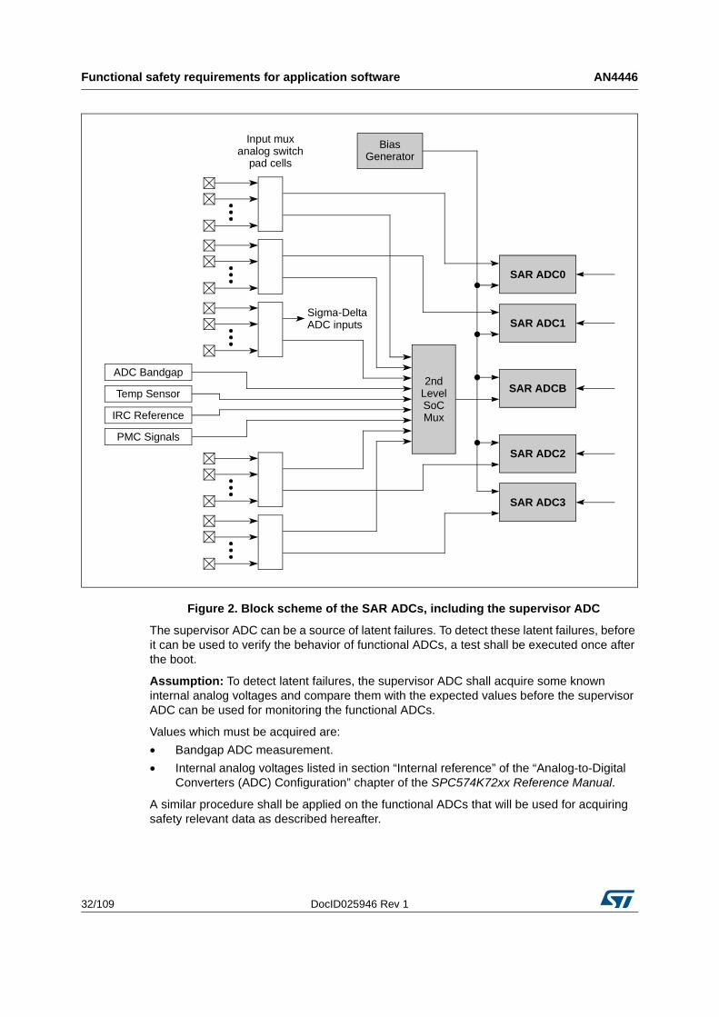
Functional safety requirements for application software AN4446
32/109 DocID025946 Rev 1
Figure 2. Block scheme of the SAR ADCs, including the supervisor ADC
The supervisor ADC can be a source of latent failures. To detect these latent failures, before it can be used to verify the behavior of functional ADCs, a test shall be executed once after the boot.
Assumption: To detect latent failures, the supervisor ADC shall acquire some known internal analog voltages and compare them with the expected values before the supervisor ADC can be used for monitoring the functional ADCs.
Values which must be acquired are:
• Bandgap ADC measurement.
• Internal analog voltages listed in section “Internal reference” of the “Analog-to-Digital Converters (ADC) Configuration” chapter of the SPC574K72xx Reference Manual.
A similar procedure shall be applied on the functional ADCs that will be used for acquiring safety relevant data as described hereafter.
Input muxanalog switch
pad cells
ADC Bandgap
Temp Sensor
IRC Reference
PMC Signals
Sigma-DeltaADC inputs
2ndLevelSoCMux
SAR ADCB
SAR ADC3
SAR ADC2
SAR ADC1
SAR ADC0
BiasGenerator
DocID025946 Rev 1 33/109
AN4446 Functional safety requirements for application software
108
Assumption: Before the safety application starts, functional ADCs shall run a conversion cycle of known signals together with the supervisor ADC. The acquired values shall be compared by software.
Note: During the self-test conversion cycle, the configuration of both functional and monitor (supervisor) ADCs shall be the same. After the self-test and during normal acquisitions, the configurations may be modified.
3.2.23 Temperature sensor (TSENS)
The SPC574K72xx includes a temperature sensor that monitors device temperature. The temperature sensor has an analog output and three digital outputs. The digital outputs signal the MC_RGM and FCCU of under temperature and overtemperature events.
Assumption: Before the safety application starts, software shall configure the digital output of the temperature sensor to trigger an event if the temperature is outside of the permitted range.
Note: FEE_TD and RES_TD registers of the PMC_dig module are used to enable the reporting of under temperature and overtemperature conditions.
3.3 Runtime checksDuring the execution of the safety function, application software is assumed to perform a set of tasks to support the detection of random hardware failures and transition the device to a Safe stateMCU in case of a failure. This section collects the assumptions software has to fulfill during runtime.
3.3.1 General requirements
The safety concept does not protect against spurious subtle timing changes (for example, due to the XBAR not parking on the safety relevant master due to other accesses). Thus, such subtle timing must not be relied on.
Assumption: During the development of safety-relevant software, counting clock cycles will not be used (for example, relying on the execution time of core assembler instructions to measure time).
Assumption: If independent data paths to or from any ViMos classified module exists, software shall use them redundantly to read or write safety related data.
An independent data path exists to access the two PBRIDGEs and application software should use the peripheral set redundantly. In this case, failures in one of the data paths will be detected by application level checks (for example, by comparing data provided by two redundantly used peripherals when each is attached to a different PBRIDGE).
Note: The “Periphery allocation” figure in the SPC574K72xx Reference Manual shows the peripheral split between the two peripheral bridges (PBRIDGEA, PBRIDGEB). Section 3.3.17: I/O and Peripheral Bridge gives additional detail about using safety relevant I/Os.
Assumption: A safety mechanism will be implemented at application level to detect critical timing failures leading to violation of application timeouts.
Note: Implementation Hint: The SWT module can be used to satisfy the above requirement.
Functional safety requirements for application software AN4446
34/109 DocID025946 Rev 1
Machine check exceptions of the safety core are directly forwarded to the FCCU’s “Safety Core Exception” input.
Recommendation: Due to the more comprehensive information available in the exception handler it is recommended to handle machine check exceptions in the exception handler and not use the FCCU mechanism.
Assumption: Other exceptions, which are not directly forwarded to the FCCU (for example, Data Storage, Alignment), must be handled by the core itself. This assumption shall be considered only for exception considered safety relevant by the application.
Note: See "Core e200z420Dn3 description" and "Core e200z225Bn3 description" chapters in the SPC574K72xx Reference Manual and the “Exceptions” sections of each chapter for details on core exceptions.
3.3.2 CRC of configuration registers
The CRC unit offloads the core in computing a CRC checksum. There are three sets of CRC registers to allow concurrent CRC computations in the SPC574K72xx device. The CRC unit should be used to detect accidental modifications of data in configuration registers by calculating its CRC signature and comparing it against a pre-calculated CRC.
Note: Some configuration registers, as those for clock and MCU mode configuration, are copied to the corresponding internal registers only when an event (for example, mode change) is triggered. The values of those configuration registers themselves have no effect. Additional measures are needed, along with CRCing, to ensure correct operation of the MCU.
Assumption: A periodic scan of the safety relevant configuration registers, which are not covered by other safety mechanisms, shall be executed once per FTTI to ensure that the configuration has not changed due to a bit flip. A list of safety relevant registers is provided in the SPC574K72xx Reference Manual’s “Functional Safety” chapter and the “Register safety classifications” table.
Note: Implementation hint: The CRC checksum of the configuration registers of the modules involved with the safety function should be calculated offline.
Note: At run time, the same CRC value must be calculated by the CRC module within the FTTI. To avoid overloading a core, the DMA module can be used to support the data transfer from the registers under check to the CRC module.
Note: The result of the runtime computation is then compared to the offline one.
CMU registers are sources of latent failures which cannot lead directly to the violation of the safety goal. The assumption below shall be considered.
Assumption: To reduce number of possible CCFs, the configuration registers of the CMU_1, used to monitor the clock source of the safety core, shall be included into the periodic register CRCing scheme.
Assumption: The two CRC units are not specifically designed to be used redundantly (for example, to check each other). In fact, there is no dependency constraint imposed on the design.
3.3.3 XBAR usage
The application software must check the XBAR configuration once after programming but it must also detect failures of the XBAR when safety-relevant functions are running.
DocID025946 Rev 1 35/109
AN4446 Functional safety requirements for application software
108
Assumption: Application software shall check the configuration of XBAR every FTTI to detect failures affecting the register interface.
Assumption: Within the FTTI, application software will detect failures of the XBAR configuration affecting system performance.
The detection of failures of the XBAR configuration can be achieved as a combination of periodic read-back of the configuration registers and control flow monitoring using the SWT. The SWT is needed to cover those failure conditions leading to a complete lock-out of XBAR masters. The need for periodic configuration read-back depends on how stringent the control flow monitoring is implemented.
XBAR data and address lines are covered by E2E ECC. Some failures, particularly those affecting muxing logic, might introduce multi-bit errors on data and addresses. Though ECC coverage is limited on a single transaction the probability of detecting the fault is higher when multiple transactions are affected.
Assumption: Safety analysis assumes that at least two transactions are affected (for example, at least two accesses are made by or to the safety relevant XBAR master(s) or slave(s) within each FTTI).
3.3.4 System Memory Protection Unit (SMPU)
The SMPU provides memory protection at the XBAR. A failure in the SMPU can change the behavior of the SMPU (for example, enabling or disabling the protection), resulting in unauthorized access to the protected data, or leading to unexpected access violations and data storage exceptions.
The protection against such failures is given by the read-back of the configuration registers, together with the exception handler and the SWT if the exception handler cannot execute. SWT and exception handlers are assumed to cover cases when accesses to system resources are unexpectedly prevented to authorized masters. On the other hand, SMPU failures resulting in missing memory protection are considered critical only if coupled with other failures causing the undesired access to protected data (notice that systematic failures, besides random HW failures, can lead to this scenario).
Assumption: Application SW checks the configuration of the SMPU every FTTI. In particular, it has to check the cacheability attribute of each region descriptor as transactions erroneously marked as cacheable may cause shared data to be cached, potentially leading to stale data in the cache.
Safety analyses are performed under the following assumptions:
• Assumption: FMEDA assumes that 90% of region descriptors are usually used during the execution of safety tasks.
• Assumption: SMPU is enabled approximately 99% of the time during the execution of safety tasks.
3.3.5 Platform flash memory controller
The PFLASH controller configuration controls aspects of read wait states, port arbitration, prefetching policy, master access and flash memory remapping.
Some of these failures only cause performance reductions, so they can be covered by the SWT.
Functional safety requirements for application software AN4446
36/109 DocID025946 Rev 1
Assumption: Safety analysis assumes that at least four reads through the PFLASH controller are executed within the FTTI.
Other configuration failures, such as master access and safe remapping, only cause MultiPoint Failures (MPF), so one time readback is sufficient.
Assumption: After configuring the PFLASH controller, the application shall read back the PFLASH controller registers and compare them with the expected values every FTTI.
3.3.6 Flash memory
Overlay operations
Overlay SRAM is included in the SPC574K72xx family of devices as part of a comprehensive set of calibration and debug features. It is recommended that overlay SRAM be used only for these tasks and not for wide scale general functionality in production since the safety mechanisms have only limited CCF protection.
Assumption: Overlay RAM is used to remap data only. No instruction fetch remapping occurs during normal operation, but this can be done during debug mode.
Writes to incorrect addresses are covered by reading back the data that was written. Reads from an incorrect source have different effects according to the selected source versus the targeted one:
• Overlay RAM, instead of flash memory, read errors can be detected by E2E ECC as the overlay read data buffer contains data fetched from a different address (with its specific addr/data ECC).
• Prefetch buffers, instead of overlay RAM, read errors can be detected by E2E ECC as the word has been prefetched from a different address.
• Flash memory, instead of overlay RAM, read errors are not detected by E2E ECC as the access is done with the correct (logical) address but can be detected by writing and reading back a few patterns from the overlay RAM.
Assumption: Software shall run write and read-back patterns from overlay RAM to check integrity of overlay read/write/selection path, and this test shall be executed every FTTI.
When overlay, or flash memory, regions are programmed, data in the mini-cache can be stale (a missed hit during write operations could lead to erroneously valid prefetched data). Reading back the data after each programming operation ensures that prefetched data are invalidated.
Assumption: After write operations to overlay RAM, or flash, software shall read back the data that was written and compare it with the expected data to check the integrity of the programmed data.
Note: These countermeasures apply only if the overlay RAM is used by the safety function.
When software reads data that was programmed in the flash memory, or written to overlay RAM (to verify contents), the mini-cache will be automatically refreshed.
Assumption: Overlay RAM is used only for a fraction of the time on a small number of devices (assumed 5%, averaged considering all MCUs).
Flash memory program and erase
Flash memory program/erase operations are stopped in the event of a fault event (for example, no flash sector selected, or elevated current draw).
DocID025946 Rev 1 37/109
AN4446 Functional safety requirements for application software
108
Assumption: For program operations, only the address specified by an interlock write determines the partition being written. An interlock sequence is used to prevent accidental programming of flash memory.
Assumption: A software safety mechanism shall be implemented to ensure the correct termination of any program/write operation of the flash memory.
Even when flash memory signals the correct termination of programming operations, there is still the chance that flash memory content is incorrect due to failures of the flash memory write path and programming logic.
Assumption: To ensure that the content of a write operation to flash memory is correct, software shall read back the data that was written and compare it with the expected data. This checks the integrity of the programmed data. This test should execute after every program or erase operation.
Note: In addition, this test prevents the return of stale data from the PFLASH controller mini-cache.
Flash memory multibit error
Nonvolatile flash memory is protected with a SBE correction/double-bit error detection (SEC/DED) ECC scheme.
Multibit errors can be caused by failures affecting common pieces of the flash memory (for example, sensing amplifier, read logic). These type of failures lead to random data reads (for example, white noise on read word). Reading random data is detected as SBE and corrected by the ECC logic(g). A software mechanism is needed to distinguish between a real SBE and a MBE.
This test consists of executing multiple reads to be run if a SBE event occurs (for example, 4 reads is sufficient). If the multiple reads trigger additional correctable/noncorrectable errors, the flash memory contains permanent multibit errors.
Assumption: If an ECC correction occurs, the application shall force the read of a number of patterns sufficient to trigger other ECC error corrections/detections revealing the actual nature of the fault (in fact, permanent flash memory control failures typically affects multiple read operations).
Note: The piece of the flash memory which can cause multibit errors are shared by the Read-While-Write (RWW) partitions of each flash memory. The multiple read shall be executed out of the affected RWW flash partition (list of flash memory RWW partitions are shown in the “Memory Map” chapter’s “Flash memory and overlay RAM map” table of the SPC574K72xx Reference Manual’s).
Note: Reading 4 patterns is sufficient to reach a DC of about 99% of coverage.
EEPROM emulation
The SPC574K72xx provides four blocks (4 × 16 KB) of the flash memory for EEPROM emulation. ECC events detected on accesses to the EEPROM flash memory blocks are not reported to the MEMU. SBEs are corrected, but not signaled to the MEMU. MBEs are replaced by a fixed word (for example, an illegal instruction) and are also not forwarded to the MEMU.
g. With a DC of about 70%.
Functional safety requirements for application software AN4446
38/109 DocID025946 Rev 1
Assumption: Software using EEPROM for storage of information will use its own information redundancy (for example, CRCs) to detect incorrect data returned from the EEPROM emulation.
3.3.7 PRAMC configuration
PRAMC provides a certain level of configurability on accessing the RAM. Faults in the PRAMC configuration registers may change PRAMC port priority and, most important, read wait states. Changes in port priorities, or more wait states, can have an impact on the overall performance, which is typically covered by using the SWT. However, fewer wait states can lead to multi-bit errors that are detected by E2E ECC with only low to medium effectiveness.
Assumption: Application software shall check the configuration of the PRAMC every FTTI.
The periodic check of PRAMC configuration can be avoided if the following assumption is satisfied:
• Assumption: Application software performs at least two accesses to the SRAM within the FTTI, or a simple test could be performed (for example, a test based on write and read-back performed every FTTI).
3.3.8 RAM
RAM is protected from failures by ECC logic with various implementations discussed in the following sections. To increase the coverage against MBE certain SW measures have been assumed.
Error Correcting Code (ECC)
Some failure modes of the RAM, for example failures affecting common part of the RAM structure, cause data to be read from all location as All-0 or All-1(h).
In such a case if a data is read out of the RAM, an event should be detected by the ECC which perceives All-X code-word as invalid code. But in the SPC574K72xx there are some RAMs whose address is included in the ECC checksum calculation to increase the diagnostic coverage in case of addressing failures.
List of memories where ECC bits are computed including address contribution can be found in the Reference Manual (please see the SPC574K72xx Reference Manual’s “ECC RAM implementation” table in the “Functional Safety” chapter).
Due to this hardware architecture there are address locations out of which reading All-X word is valid and no ECC event is triggered(i). Approximately there is one of these addresses out of 256 ones.
Assumption: There is no special handling of All-X words for ECC that includes addresses in the ECC code-bit calculation. They can be valid, correctable or uncorrectable words depending on the address.
h. All-0 and All-1 will be referenced generically as All-X.
i. For the sake of simplicity, let us call “All-X addresses” the ones which perceive All-X as valid and “Normal addresses” the remaining ones.
DocID025946 Rev 1 39/109
AN4446 Functional safety requirements for application software
108
Consider a permanent All-X failure mode:
• If there is a transaction to a “normal address”, this failure mode is detected by the ECC which perceives the All-X code-word as invalid (either single bit error or correction is triggered).
• If there is a transaction to an “All-X address”, this failures mode is not detected by the ECC or other means (All-X code-word is valid for “All-X address”).
The permanent All-X failure mode is not detected by the ECC if an application reads only All-X addresses of the RAM. This is a pure theoretical case because a real application doesn't read only such All-X addresses, but reads different parts of the RAM including (and mainly) normal addresses.
Within the FTTI, application software shall read in each RAM block two addresses that are known to cause an uncorrectable error in case the memory globally shows an All-0 or an All-1 state.
Note: Real application continuously reads several RAM locations (both normal and All-X addresses) in different RAM blocks. Some of these transactions are directed to addresses which trigger uncorrectable error in case of All-X events.
Note: As result in most of cases the assumption above is satisfied by the application accessing RAM during the normal code execution without any additional overhead in terms of both coding and timing.
The program in Section 6: Testing All-X in RAM, calculates the list of addresses, which trigger uncorrectable errors if an All-0 (or an All-1) failure occurs, by a linear search from a start address. These locations shall be used to verify the presence of a global All-0 (or All-1) error.
The user can verify that the application software reads, once per FTTI, at least one location to detect a global All-0 errors and one location to detect for All-1. In that case additional readings of previous assumption are not necessary.
Assumption: SW shall ensure that data in Standby RAM is additionally protected (for example, with an application-level checksum) against effects occurring during standby, especially the aggregation of several Single Bit Upsets (SBUs) and the possibility of power failures.
Repair logic
Memory repair faults can cause a partial shift of the word. This failure mode can affect one word or an entire column depending on the type of failure in the repaired column (single bit in array or column periphery). If a read operation is performed first, this will result in a MBE (white noise model). In the event a write operation to a specific address was executed first after this error resulted, any subsequent read of that same address will be either correct or result in a SBE.
Assumption: To guarantee coverage for MBEs it is assumed at least four reads on different addresses per RAM block and FTTI will occur. This provides sufficient Diagnostic Coverage for column repair with ECC.
Error reporting
The MEMU collects and reports error events associated with ECC logic used on system RAM, peripheral RAM and flash memory. The MEMU stores the addresses where ECC errors occurred. The MEMU also reports whether the error is correctable vs. uncorrectable. Uncorrectable errors will cause a report to the FCCU.
Functional safety requirements for application software AN4446
40/109 DocID025946 Rev 1
Correctable errors include:
• Single-bit error in the data part that is detected via ECC for a system RAM, peripheral RAM or flash memory
• Single-bit error in the data part that is detected via MBIST on any RAM
Uncorrectable errors include:
• Multi-bit error that is detected via ECC for a system RAM, peripheral RAM or flash memory
• Multi-bit error that is detected via MBIST on any SRAM
• Addressing errors and unused data bit errors detected by ECC logic
Failures in RAM logic (for example, decoding, control, and so on) might lead to MBEs (white noise model). Faults can have two kinds of effects:
• Always result in a random data pattern when the content of the faulty address is read (for example, no word lines selection, clocking failure)
• Cause MBEs only on transactions targeting a subset of RAM addresses (for example, multiple word lines selection)
In both cases above, ECC logic can lead to a wrong correction. It is necessary to implement a software test to detect permanent MBE sources leading to erroneous ECC corrections, so the overall coverage (ECC + software test) is the same as that provided by a 64 / 8 EDC scheme (for example (1 - 1 / 256 × 100.0%) = 99.6%).
Assumption: In the first case (on page 40) a software test shall be implemented to detect permanent MBE sources. It will fetch the error address of corrected errors from the MEMU and assess the nature of the fault by writing and reading back a few patterns (for example, two's-complemented patterns) to the faulty location. The software test shall be executed within the FTTI after a new ECC error correction in RAM is reported.
Assumption: For the second case (on page 40) a software test shall be implemented to detect permanent MBE sources caused by multiple address selections. It will fetch the error address of corrected errors from the MEMU and assess the nature of the fault by writing and reading back a (small) set of patterns to multiple locations depending on the faulty address.
Note: This test is described in Section 5.5, TEST4: multiple addresses (bridging) using fixed set of addresses.
Assumption: These software tests will be executed within the FTTI after a new ECC error correction in RAM is reported.
Assumption: During operation, if the MEMU contains two entries for the same address of an address which is part of a memory for which ECC syndromes are reported, SW will check whether one of the two syndromes is FFh. If so, this entry should be deleted. This entry came from another ECC unit which does not report syndromes. As long as the entry with the correct syndrome is stored in the MEMU, entries for the same address without syndrome will not be stored.
3.3.9 ECC Bypass using core registers and Indirect Memory Access (IMA)
During test, or development, the need for direct access to all RAM bits that is not filtered through the ECC logic may arise. Memory locations can be accessed directly either via processor core access or the IMA module (see the SPC574K72xx Reference Manual’s “Indirect Memory Access (IMA)” chapter).
DocID025946 Rev 1 41/109
AN4446 Functional safety requirements for application software
108
This mechanism provides access to all bits in the RAM arrays, therefore allows reading and manipulating of ECC check bits. In general, the core mechanism needs to be used for core accessible RAM, whereas the IMA module is responsible for granting direct access to other RAMs (typical peripheral).
Accesses via the IMA module are not controlled by the MPU, but the MPU controls access to this module. Direct accesses using the core mechanism are normally controlled by the MPU.
Assumption: Software shall ensure that no other RAM access occurs to a certain array while the IMA module is used to access the contained RAM cells directly.
Assumption: Software shall check that ECC bypassing mechanisms are executed only when the ECC manipulation is really expected and not due to some software control flow problem.
3.3.10 Decorated Storage Memory Controller (DSMC)
DSMC gives the hardware support to have atomic read-modify-write memory operations in the SPC574K72xx microcontroller. These capabilities are called decorated storage.
FMEDA assumes some limitations on the usage of the DSMC.
Assumption: The use of decorated storage transaction is limited to the Safety core (Main Core_0 and Checker Core_0) local memory. The usage of decorated storage transaction on other memories is forbidden.
Note: DSMC connected to the Safety core is part of the delayed lockstep redundancy and any fault will be detected by RCCU.
Note: It is currently under investigation whether the prohibition of DSMC use on other memories relates only to safety software or to all software.
3.3.11 Interrupt management
No specific hardware protection is provided against spurious or missing interrupt requests (for example, caused by EMI on the interrupt lines or bit flips in the interrupt registers of the peripherals). The Interrupt Controller (INTC) can drop, delay or create interrupts.
To detect these unwanted events different software measure need to be considered:
• Assumption: Periodically check for effects of lost interrupts (for example, buffer overflow or underflow).
• Assumption: Periodically check that interrupt flags in peripherals are cleared.
– This works specifically well if done outside an IRQ routine or with very low IRQ priority. If a flag for an interrupt (with higher priority) is set, this is an error. No IRQs shall be blocked while this test is executed.
• Assumption: The ISR will check that the triggering module actually shows a requested interrupt (for example, reading the interrupt request or status register in the peripheral).
• Assumption: The ISR shall check that it was called with the correct priority.
• Assumption: Interrupts where a short latency is safety-relevant are assigned to two (or more) cores and one of those cores checks (for example, using a shared variable) that the other core actually executes the ISR within the expected latency after the IRQ occured.
• Assumption: The ISR checks that it is executed on the expected core using the relevant core register.
Functional safety requirements for application software AN4446
42/109 DocID025946 Rev 1
Note: The application software can determine the core that is presently running software by reading the Processor ID Register (PIR) (see e200z4xx Core Reference Manual for details).
• Assumption: Unused interrupt vectors shall point, or jump, to an address which is illegal to execute, contains an illegal instruction, or in some other way causes detection of their execution.
Note: Example implementations of this software and further information on it can be found in a future white paper.
3.3.12 eDMA usage
The DMA provides the capability to perform data transfers with minimal intervention from the core. It supports programmable source and destination addresses and transfer size.
Since DMA is NoSaMo, no safety measure has been implemented in HW. It is the task of the application software to provide any necessary safety measures due to safety-relevant usage of the eDMA.
3.3.13 Reset Generation Module (MC_RGM)
MC_RGM can trigger interrupts or request a transition to SAFE mode, if the MC_RGM is configured to do so.
Assumption: To detect spurious interrupts or transition requests to SAFE mode, the interrupt handler, for IRQs coming from the MC_RGM, will check that the shown source is one which was configured to cause such a request from the MC_RGM (for example, compare the MC_RGM_FES register to the expected MC_RGM_FERD and MC_RGM_FEAR register contents).
Note: If the MC_RGM triggers a transition request to SAFE mode, no interrupt is triggered by the MC_RGM. An interrupt will be triggered by the MC_ME.
3.3.14 Detection of unwanted resets
MC_RGM allows triggering individual resets for MCU modules (for example, using the Peripheral Reset Registers (RGM_PRST[n]). This can be prohibited by using the access control mechanisms of the SPC574K72xx such as the MPU or PAC. In case those are not used, and also to detect spurious resets caused by SEE, the following describes how such spurious resets can be detected.
Assumption: To detect unwanted reset of these modules, software and hardware counter measures can be applied. Table 2 summarizes these counter measures.
This is a brief description of each of the column headings in Table 2:
• Reset Signal – The internal signal that resets one or more of the receiving modules.
• Receiving Module – This module is reset by the specified reset signal in the “Reset Signal” column.
• Software Control – The register (or registers) which can reset the specified “Receiving Module” by the specified “Reset Signal”. If no register is listed, the specified “Reset Signal” cannot be controlled by the register interface.
• Reset effect and Detectability – The effect of the unwanted reset of the specified “Receiving Module” and shows some mechanisms that can detect the module where
DocID025946 Rev 1 43/109
AN4446 Functional safety requirements for application software
108
the event occurred. If multiple mechanisms are listed, the software can choose the mechanism that better fits its need (unless explicitly specified).
• Specific software action needed – Additional software mechanism, with respect to the application software, required to detect an unwanted reset of the specified “Receiving Module” (for example, polling coming from configuration registers).
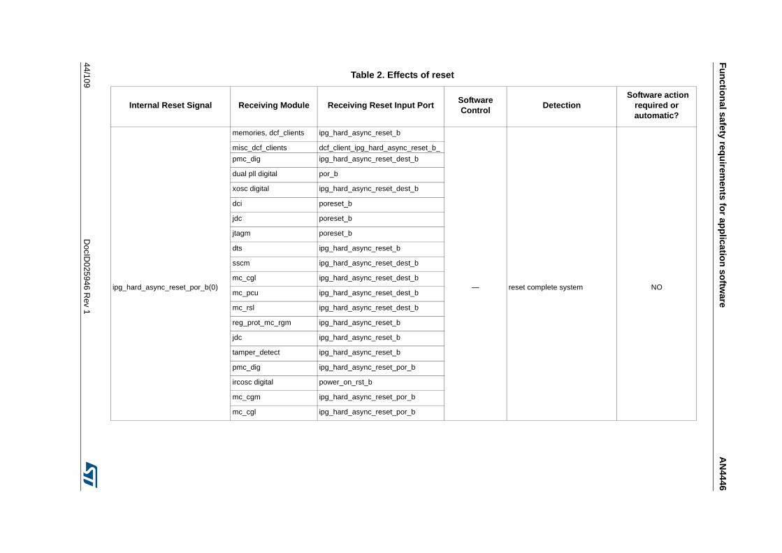
Fu
nctio
nal safety req
uirem
ents fo
r app
lication
softw
areA
N4446
44/109D
ocID025946 R
ev 1
Table 2. Effects of reset
Internal Reset Signal Receiving Module Receiving Reset Input PortSoftware Control
Detection Software action
required or automatic?
ipg_hard_async_reset_por_b(0)
memories, dcf_clients ipg_hard_async_reset_b
— reset complete system NO
misc_dcf_clients dcf_client_ipg_hard_async_reset_b_
pmc_dig ipg_hard_async_reset_dest_b
dual pll digital por_b
xosc digital ipg_hard_async_reset_dest_b
dci poreset_b
jdc poreset_b
jtagm poreset_b
dts ipg_hard_async_reset_b
sscm ipg_hard_async_reset_dest_b
mc_cgl ipg_hard_async_reset_dest_b
mc_pcu ipg_hard_async_reset_dest_b
mc_rsl ipg_hard_async_reset_dest_b
reg_prot_mc_rgm ipg_hard_async_reset_b
jdc ipg_hard_async_reset_b
tamper_detect ipg_hard_async_reset_b
pmc_dig ipg_hard_async_reset_por_b
ircosc digital power_on_rst_b
mc_cgm ipg_hard_async_reset_por_b
mc_cgl ipg_hard_async_reset_por_b
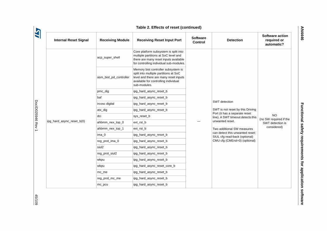
AN
4446F
un
ction
al safety requ
iremen
ts for ap
plicatio
n so
ftware
DocID
025946 Rev 1
45/109
ipg_hard_async_reset_b(0)
acp_super_shell
Core platform subsystem is split into multiple partitions at SoC level and there are many reset inputs available for controlling individual sub-modules.
—
SWT detection SWT is not reset by this Driving Port (it has a separate reset line). A SWT timeout detects this unwanted reset. Two additional SW measures can detect this unwanted reset: SIUL cfg read-back (optional) CMU cfg (CMErst=0) (optional)
NO(no SW required if the
SWT detection is considered)
asm_bist_pd_controller
Memory bist controller subsystem is split into multiple partitions at SoC level and there are many reset inputs available for controlling individual sub-modules.
pmc_dig ipg_hard_async_reset_b
baf ipg_hard_async_reset_b
ircosc digital ipg_hard_async_reset_b
atx_dig ipg_hard_async_reset_b
dci sys_reset_b
ahbmm_nex_top_0 ext_rst_b
ahbmm_nex_top_1 ext_rst_b
ima_0 ipg_hard_async_reset_b
reg_prot_ima_0 ipg_hard_async_reset_b
siul2 ipg_hard_async_reset_b
reg_prot_siul2 ipg_hard_async_reset_b
wkpu ipg_hard_async_reset_b
wkpu ipg_hard_async_reset_core_b
mc_me ipg_hard_async_reset_b
reg_prot_mc_me ipg_hard_async_reset_b
mc_pcu ipg_hard_async_reset_b
Table 2. Effects of reset (continued)
Internal Reset Signal Receiving Module Receiving Reset Input PortSoftware Control
Detection Software action
required or automatic?
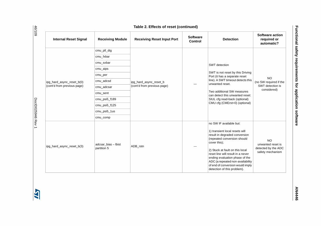
Fu
nctio
nal safety req
uirem
ents fo
r app
lication
softw
areA
N4446
46/109D
ocID025946 R
ev 1
ipg_hard_async_reset_b(0)(cont’d from previous page)
cmu_pll_dig
ipg_hard_async_reset_b(cont’d from previous page)
—
SWT detection SWT is not reset by this Driving Port (it has a separate reset line). A SWT timeout detects this unwanted reset. Two additional SW measures can detect this unwanted reset: SIUL cfg read-back (optional) CMU cfg (CMErst=0) (optional)
NO(no SW required if the
SWT detection is considered)
cmu_fxbar
cmu_sxbar
cmu_aips
cmu_per
cmu_adcsd
cmu_adcsar
cmu_sent
cmu_psi5_f189
cmu_psi5_f125
cmu_psi5_1us
cmu_comp
ipg_hard_async_reset_b(3)adcsar_bias – lbist partition 5
ADB_rstn —
no SW IF available but: 1) transient local resets will result in degraded conversion (repeated conversion should cover this); 2) Stuck at fault on this local reset line will result in a never ending evaluation phase of the ADC (a repeated non-availability of end of conversion would imply detection of this problem).
NOunwanted reset is
detected by the ADC safety mechanism
Table 2. Effects of reset (continued)
Internal Reset Signal Receiving Module Receiving Reset Input PortSoftware Control
Detection Software action
required or automatic?
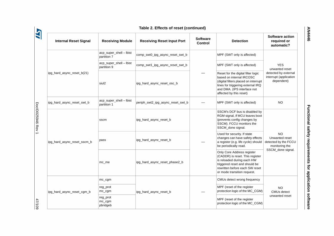
AN
4446F
un
ction
al safety requ
iremen
ts for ap
plicatio
n so
ftware
DocID
025946 Rev 1
47/109
ipg_hard_async_reset_b(21)
acp_super_shell – lbist partition 7
comp_swt0_ipg_async_reset_swt_b
—
MPF (SWT only is affected)
YESunwanted reset
detected by external interrupt (application
dependent)
acp_super_shell – lbist partition 9
comp_swt1_ipg_async_reset_swt_b MPF (SWT only is affected)
siul2 ipg_hard_async_reset_osc_b
Reset for the digital filter logic based on internal IRCOSC (digital filters placed on interrupt lines for triggering external IRQ and DMA. (IPS interface not affected by this reset)
ipg_hard_async_reset_swt_bacp_super_shell – lbist partition 1
periph_swt2_ipg_async_reset_swt_b — MPF (SWT only is affected) NO
ipg_hard_async_reset_sscm_b
sscm ipg_hard_async_reset_b
—
SSCM's DCF bus is disabled by RGM signal, if MCU leaves boot (prevents config changes by SSCM). FCCU monitors the SSCM_done signal.
NOUnwanted reset
detected by the FCCU monitoring the
SSCM_done signal.
pass ipg_hard_async_reset_b
Used for security. If state changes can have safety effects a register (e.g. life cycle) should be periodically read.
mc_me ipg_hard_async_reset_phase2_b
Only Core Address register (CADDR) is reset. This register is reloaded during each HW triggered reset and should be rewritten before each SW reset or mode transition request.
ipg_hard_async_reset_cgm_b
mc_cgm
ipg_hard_async_reset_b —
CMUs detect wrong frequency
NOCMUs detect
unwanted reset
reg_prot mc_cgm
MPF (reset of the register protection logic of the MC_CGM)
reg_prot mc_cgm pbridgeb
MPF (reset of the register protection logic of the MC_CGM)
Table 2. Effects of reset (continued)
Internal Reset Signal Receiving Module Receiving Reset Input PortSoftware Control
Detection Software action
required or automatic?
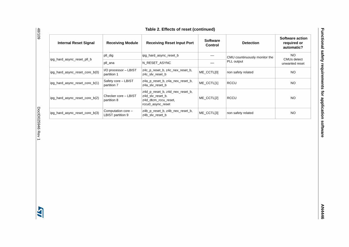
Fu
nctio
nal safety req
uirem
ents fo
r app
lication
softw
areA
N4446
48/109D
ocID025946 R
ev 1
ipg_hard_async_reset_pll_bpll_dig ipg_hard_async_reset_b — CMU countinuously monitor the
PLL output
NOCMUs detect
unwanted resetpll_ana N_RESET_ASYNC —
ipg_hard_async_reset_core_b(0)I/O processor – LBIST partition 1
z4c_p_reset_b, z4c_nex_reset_b, z4c_slv_reset_b
ME_CCTL[0] non safety related NO
ipg_hard_async_reset_core_b(1)Safety core – LBIST partition 7
z4a_p_reset_b, z4a_nex_reset_b, z4a_slv_reset_b
ME_CCTL[1] RCCU NO
ipg_hard_async_reset_core_b(2)Checker core – LBIST partition 8
z4d_p_reset_b, z4d_nex_reset_b, z4d_slv_reset_b. z4d_dtcm_rccu_reset, rccu0_async_reset
ME_CCTL[2] RCCU NO
ipg_hard_async_reset_core_b(3)Computation core – LBIST partition 9
z4b_p_reset_b, z4b_nex_reset_b, z4b_slv_reset_b
ME_CCTL[3] non safety related NO
Table 2. Effects of reset (continued)
Internal Reset Signal Receiving Module Receiving Reset Input PortSoftware Control
Detection Software action
required or automatic?
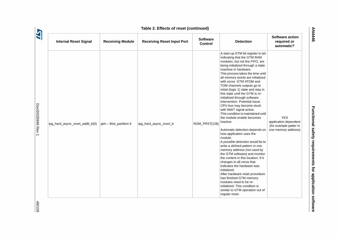
AN
4446F
un
ction
al safety requ
iremen
ts for ap
plicatio
n so
ftware
DocID
025946 Rev 1
49/109
ipg_hard_async_reset_addtl_b(0) gtm – lbist_partition 6 ipg_hard_async_reset_b RGM_PRST[128]
A start-up GTM bit register is set indicating that the GTM RAM modules, but not the FIFO, are being initialized through a state machine in hardware. This process takes the time until all memory words are initialized with zeros. GTM ATOM and TOM channels outputs go to initial (logic 1) state and stay in this state until the GTM is re-initialized through software intervention. Potential issue: CPU bus may become stuck with WAIT signal active. This condition is maintained until the module enable becomes inactive.
Automatic detection depends on how application uses the module. A possible detection would be to write a defined pattern in one memory address (not used by the GTM software) and monitor the content in this location. If it changes to all zeros that indicates the hardware was initialized. After hardware reset procedure has finished GTM memory modules need to be re-initialized. This condition is similar to GTM operation out of regular reset.
YESapplication dependent (for example patter in one memory address)
Table 2. Effects of reset (continued)
Internal Reset Signal Receiving Module Receiving Reset Input PortSoftware Control
Detection Software action
required or automatic?
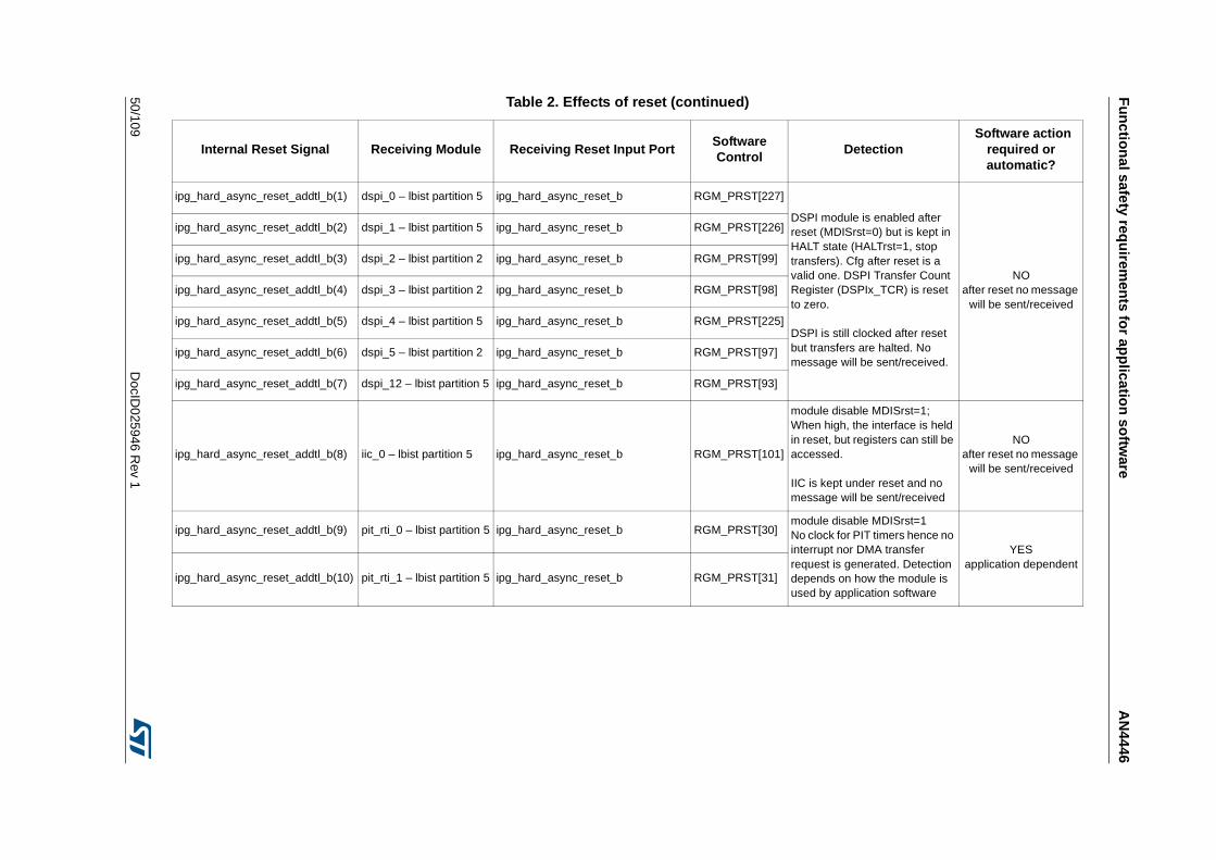
Fu
nctio
nal safety req
uirem
ents fo
r app
lication
softw
areA
N4446
50/109D
ocID025946 R
ev 1
ipg_hard_async_reset_addtl_b(1) dspi_0 – lbist partition 5 ipg_hard_async_reset_b RGM_PRST[227]
DSPI module is enabled after reset (MDISrst=0) but is kept in HALT state (HALTrst=1, stop transfers). Cfg after reset is a valid one. DSPI Transfer Count Register (DSPIx_TCR) is reset to zero. DSPI is still clocked after reset but transfers are halted. No message will be sent/received.
NOafter reset no message
will be sent/received
ipg_hard_async_reset_addtl_b(2) dspi_1 – lbist partition 5 ipg_hard_async_reset_b RGM_PRST[226]
ipg_hard_async_reset_addtl_b(3) dspi_2 – lbist partition 2 ipg_hard_async_reset_b RGM_PRST[99]
ipg_hard_async_reset_addtl_b(4) dspi_3 – lbist partition 2 ipg_hard_async_reset_b RGM_PRST[98]
ipg_hard_async_reset_addtl_b(5) dspi_4 – lbist partition 5 ipg_hard_async_reset_b RGM_PRST[225]
ipg_hard_async_reset_addtl_b(6) dspi_5 – lbist partition 2 ipg_hard_async_reset_b RGM_PRST[97]
ipg_hard_async_reset_addtl_b(7) dspi_12 – lbist partition 5 ipg_hard_async_reset_b RGM_PRST[93]
ipg_hard_async_reset_addtl_b(8) iic_0 – lbist partition 5 ipg_hard_async_reset_b RGM_PRST[101]
module disable MDISrst=1; When high, the interface is held in reset, but registers can still be accessed. IIC is kept under reset and no message will be sent/received
NOafter reset no message
will be sent/received
ipg_hard_async_reset_addtl_b(9) pit_rti_0 – lbist partition 5 ipg_hard_async_reset_b RGM_PRST[30]module disable MDISrst=1 No clock for PIT timers hence no interrupt nor DMA transfer request is generated. Detection depends on how the module is used by application software
YESapplication dependent
ipg_hard_async_reset_addtl_b(10) pit_rti_1 – lbist partition 5 ipg_hard_async_reset_b RGM_PRST[31]
Table 2. Effects of reset (continued)
Internal Reset Signal Receiving Module Receiving Reset Input PortSoftware Control
Detection Software action
required or automatic?
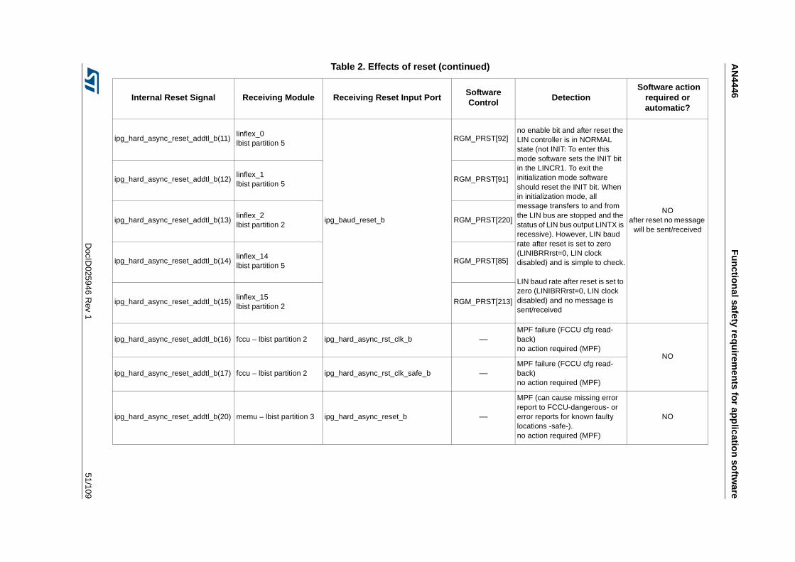
AN
4446F
un
ction
al safety requ
iremen
ts for ap
plicatio
n so
ftware
DocID
025946 Rev 1
51/109
ipg_hard_async_reset_addtl_b(11)linflex_0 lbist partition 5
ipg_baud_reset_b
RGM_PRST[92]no enable bit and after reset the LIN controller is in NORMAL state (not INIT: To enter this mode software sets the INIT bit in the LINCR1. To exit the initialization mode software should reset the INIT bit. When in initialization mode, all message transfers to and from the LIN bus are stopped and the status of LIN bus output LINTX is recessive). However, LIN baud rate after reset is set to zero (LINIBRRrst=0, LIN clock disabled) and is simple to check.
LIN baud rate after reset is set to zero (LINIBRRrst=0, LIN clock disabled) and no message is sent/received
NOafter reset no message
will be sent/received
ipg_hard_async_reset_addtl_b(12)linflex_1 lbist partition 5
RGM_PRST[91]
ipg_hard_async_reset_addtl_b(13)linflex_2 lbist partition 2
RGM_PRST[220]
ipg_hard_async_reset_addtl_b(14)linflex_14 lbist partition 5
RGM_PRST[85]
ipg_hard_async_reset_addtl_b(15)linflex_15 lbist partition 2
RGM_PRST[213]
ipg_hard_async_reset_addtl_b(16) fccu – lbist partition 2 ipg_hard_async_rst_clk_b —MPF failure (FCCU cfg read-back) no action required (MPF)
NO
ipg_hard_async_reset_addtl_b(17) fccu – lbist partition 2 ipg_hard_async_rst_clk_safe_b —MPF failure (FCCU cfg read-back) no action required (MPF)
ipg_hard_async_reset_addtl_b(20) memu – lbist partition 3 ipg_hard_async_reset_b —
MPF (can cause missing error report to FCCU-dangerous- or error reports for known faulty locations -safe-).no action required (MPF)
NO
Table 2. Effects of reset (continued)
Internal Reset Signal Receiving Module Receiving Reset Input PortSoftware Control
Detection Software action
required or automatic?
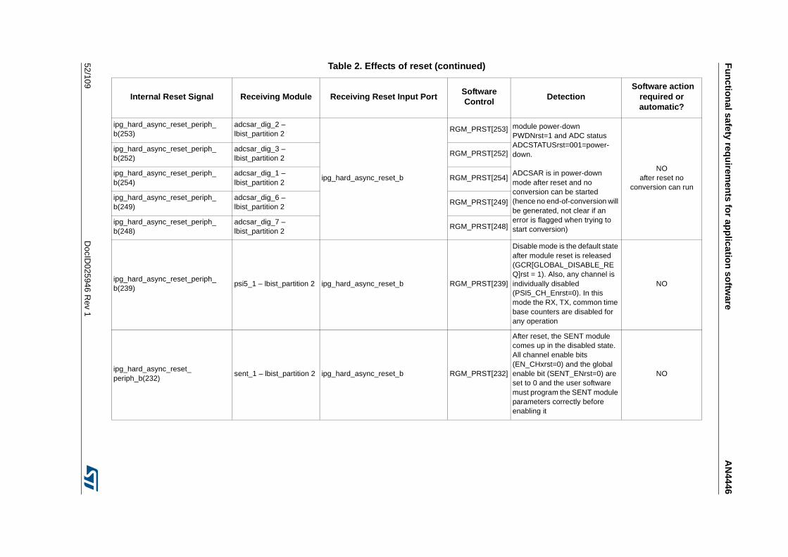
Fu
nctio
nal safety req
uirem
ents fo
r app
lication
softw
areA
N4446
52/109D
ocID025946 R
ev 1
ipg_hard_async_reset_periph_ b(253)
adcsar_dig_2 – lbist_partition 2
ipg_hard_async_reset_b
RGM_PRST[253] module power-down PWDNrst=1 and ADC status ADCSTATUSrst=001=power-down.
ADCSAR is in power-down mode after reset and no conversion can be started (hence no end-of-conversion will be generated, not clear if an error is flagged when trying to start conversion)
NOafter reset no
conversion can run
ipg_hard_async_reset_periph_ b(252)
adcsar_dig_3 – lbist_partition 2
RGM_PRST[252]
ipg_hard_async_reset_periph_ b(254)
adcsar_dig_1 – lbist_partition 2
RGM_PRST[254]
ipg_hard_async_reset_periph_ b(249)
adcsar_dig_6 – lbist_partition 2
RGM_PRST[249]
ipg_hard_async_reset_periph_ b(248)
adcsar_dig_7 – lbist_partition 2
RGM_PRST[248]
ipg_hard_async_reset_periph_ b(239)
psi5_1 – lbist_partition 2 ipg_hard_async_reset_b RGM_PRST[239]
Disable mode is the default state after module reset is released (GCR[GLOBAL_DISABLE_REQ]rst = 1). Also, any channel is individually disabled (PSI5_CH_Enrst=0). In this mode the RX, TX, common time base counters are disabled for any operation
NO
ipg_hard_async_reset_ periph_b(232)
sent_1 – lbist_partition 2 ipg_hard_async_reset_b RGM_PRST[232]
After reset, the SENT module comes up in the disabled state. All channel enable bits (EN_CHxrst=0) and the global enable bit (SENT_ENrst=0) are set to 0 and the user software must program the SENT module parameters correctly before enabling it
NO
Table 2. Effects of reset (continued)
Internal Reset Signal Receiving Module Receiving Reset Input PortSoftware Control
Detection Software action
required or automatic?
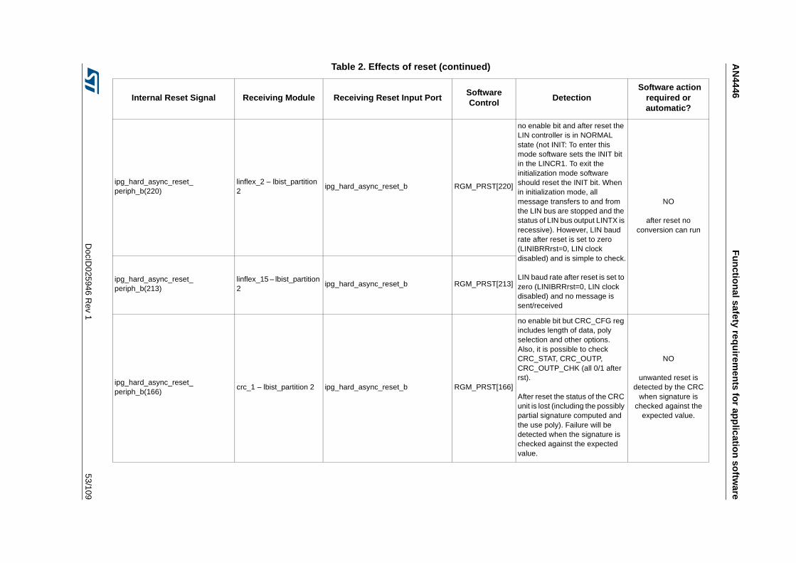
AN
4446F
un
ction
al safety requ
iremen
ts for ap
plicatio
n so
ftware
DocID
025946 Rev 1
53/109
ipg_hard_async_reset_ periph_b(220)
linflex_2 – lbist_partition 2
ipg_hard_async_reset_b RGM_PRST[220]
no enable bit and after reset the LIN controller is in NORMAL state (not INIT: To enter this mode software sets the INIT bit in the LINCR1. To exit the initialization mode software should reset the INIT bit. When in initialization mode, all message transfers to and from the LIN bus are stopped and the status of LIN bus output LINTX is recessive). However, LIN baud rate after reset is set to zero (LINIBRRrst=0, LIN clock disabled) and is simple to check.
LIN baud rate after reset is set to zero (LINIBRRrst=0, LIN clock disabled) and no message is sent/received
NO
after reset no conversion can run
ipg_hard_async_reset_ periph_b(213)
linflex_15 – lbist_partition 2
ipg_hard_async_reset_b RGM_PRST[213]
ipg_hard_async_reset_ periph_b(166)
crc_1 – lbist_partition 2 ipg_hard_async_reset_b RGM_PRST[166]
no enable bit but CRC_CFG reg includes length of data, poly selection and other options. Also, it is possible to check CRC_STAT, CRC_OUTP, CRC_OUTP_CHK (all 0/1 after rst).
After reset the status of the CRC unit is lost (including the possibly partial signature computed and the use poly). Failure will be detected when the signature is checked against the expected value.
NO
unwanted reset is detected by the CRC
when signature is checked against the
expected value.
Table 2. Effects of reset (continued)
Internal Reset Signal Receiving Module Receiving Reset Input PortSoftware Control
Detection Software action
required or automatic?
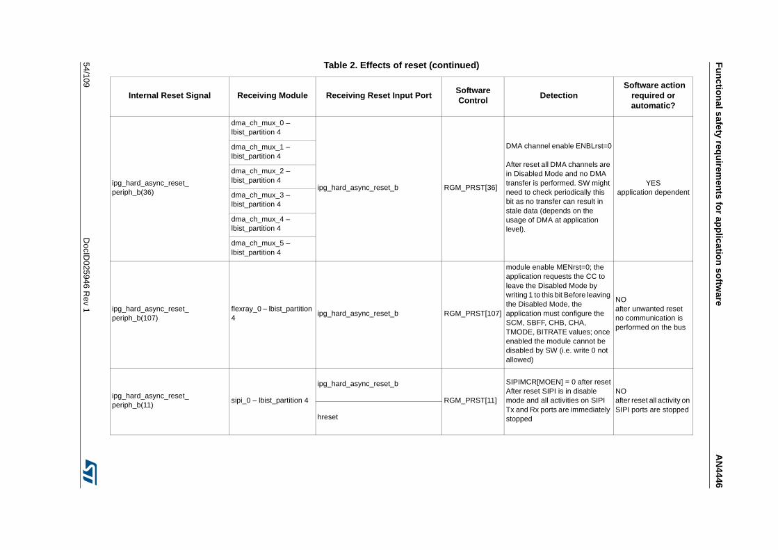
Fu
nctio
nal safety req
uirem
ents fo
r app
lication
softw
areA
N4446
54/109D
ocID025946 R
ev 1
ipg_hard_async_reset_ periph_b(36)
dma_ch_mux_0 – lbist_partition 4
ipg_hard_async_reset_b RGM_PRST[36]
DMA channel enable ENBLrst=0
After reset all DMA channels are in Disabled Mode and no DMA transfer is performed. SW might need to check periodically this bit as no transfer can result in stale data (depends on the usage of DMA at application level).
YESapplication dependent
dma_ch_mux_1 – lbist_partition 4
dma_ch_mux_2 – lbist_partition 4
dma_ch_mux_3 – lbist_partition 4
dma_ch_mux_4 – lbist_partition 4
dma_ch_mux_5 – lbist_partition 4
ipg_hard_async_reset_ periph_b(107)
flexray_0 – lbist_partition 4
ipg_hard_async_reset_b RGM_PRST[107]
module enable MENrst=0; the application requests the CC to leave the Disabled Mode by writing 1 to this bit Before leaving the Disabled Mode, the application must configure the SCM, SBFF, CHB, CHA, TMODE, BITRATE values; once enabled the module cannot be disabled by SW (i.e. write 0 not allowed)
NOafter unwanted reset no communication is performed on the bus
ipg_hard_async_reset_ periph_b(11)
sipi_0 – lbist_partition 4
ipg_hard_async_reset_b
RGM_PRST[11]
SIPIMCR[MOEN] = 0 after resetAfter reset SIPI is in disable mode and all activities on SIPI Tx and Rx ports are immediately stopped
NOafter reset all activity on SIPI ports are stopped
hreset
Table 2. Effects of reset (continued)
Internal Reset Signal Receiving Module Receiving Reset Input PortSoftware Control
Detection Software action
required or automatic?
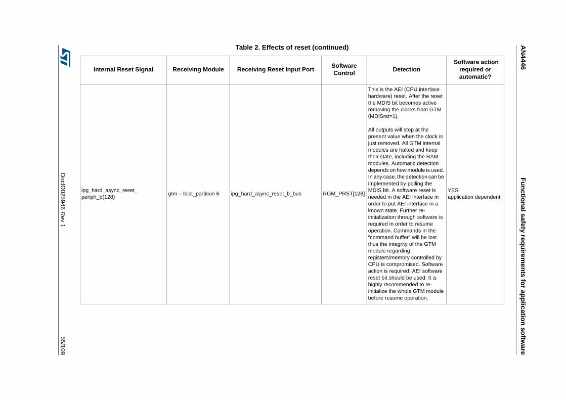
AN
4446F
un
ction
al safety requ
iremen
ts for ap
plicatio
n so
ftware
DocID
025946 Rev 1
55/109
ipg_hard_async_reset_ periph_b(128)
gtm – lbist_partition 6 ipg_hard_async_reset_b_bus RGM_PRST[128]
This is the AEI (CPU interface hardware) reset. After the reset the MDIS bit becomes active removing the clocks from GTM (MDISrst=1).
All outputs will stop at the present value when the clock is just removed. All GTM internal modules are halted and keep their state, including the RAM modules. Automatic detection depends on how module is used. In any case, the detection can be implemented by polling the MDIS bit. A software reset is needed in the AEI interface in order to put AEI interface in a known state. Further re-initialization through software is required in order to resume operation. Commands in the “command buffer” will be lost thus the integrity of the GTM module regarding registers/memory controlled by CPU is compromised. Software action is required: AEI software reset bit should be used. It is highly recommended to re-initialize the whole GTM module before resume operation.
YESapplication dependent
Table 2. Effects of reset (continued)
Internal Reset Signal Receiving Module Receiving Reset Input PortSoftware Control
Detection Software action
required or automatic?
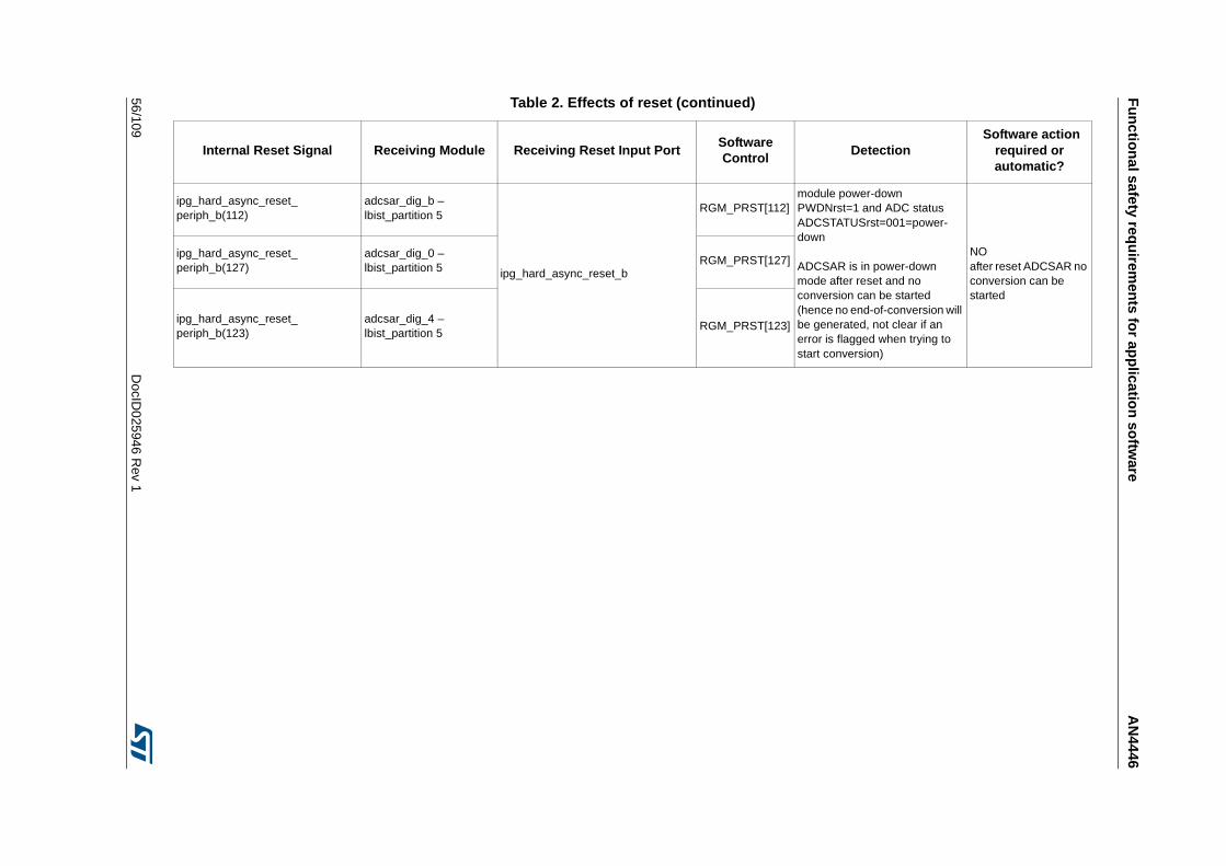
Fu
nctio
nal safety req
uirem
ents fo
r app
lication
softw
areA
N4446
56/109D
ocID025946 R
ev 1
ipg_hard_async_reset_ periph_b(112)
adcsar_dig_b – lbist_partition 5
ipg_hard_async_reset_b
RGM_PRST[112]module power-down PWDNrst=1 and ADC status ADCSTATUSrst=001=power-down
ADCSAR is in power-down mode after reset and no conversion can be started (hence no end-of-conversion will be generated, not clear if an error is flagged when trying to start conversion)
NOafter reset ADCSAR no conversion can be started
ipg_hard_async_reset_ periph_b(127)
adcsar_dig_0 – lbist_partition 5
RGM_PRST[127]
ipg_hard_async_reset_ periph_b(123)
adcsar_dig_4 – lbist_partition 5
RGM_PRST[123]
Table 2. Effects of reset (continued)
Internal Reset Signal Receiving Module Receiving Reset Input PortSoftware Control
Detection Software action
required or automatic?
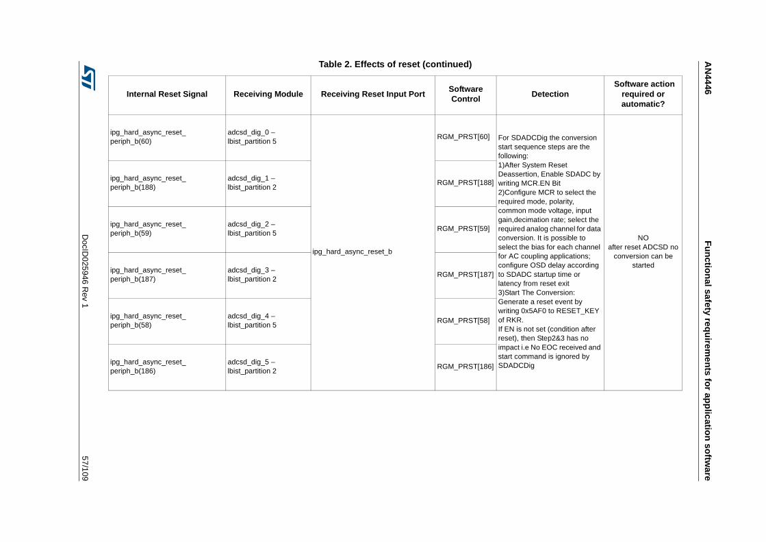
AN
4446F
un
ction
al safety requ
iremen
ts for ap
plicatio
n so
ftware
DocID
025946 Rev 1
57/109
ipg_hard_async_reset_ periph_b(60)
adcsd_dig_0 – lbist_partition 5
ipg_hard_async_reset_b
RGM_PRST[60] For SDADCDig the conversion start sequence steps are the following:1)After System Reset Deassertion, Enable SDADC by writing MCR.EN Bit2)Configure MCR to select the required mode, polarity, common mode voltage, input gain,decimation rate; select the required analog channel for data conversion. It is possible to select the bias for each channel for AC coupling applications; configure OSD delay according to SDADC startup time or latency from reset exit3)Start The Conversion: Generate a reset event by writing 0x5AF0 to RESET_KEY of RKR.If EN is not set (condition after reset), then Step2&3 has no impact i.e No EOC received and start command is ignored by SDADCDig
NOafter reset ADCSD no
conversion can be started
ipg_hard_async_reset_ periph_b(188)
adcsd_dig_1 – lbist_partition 2
RGM_PRST[188]
ipg_hard_async_reset_ periph_b(59)
adcsd_dig_2 – lbist_partition 5
RGM_PRST[59]
ipg_hard_async_reset_ periph_b(187)
adcsd_dig_3 – lbist_partition 2
RGM_PRST[187]
ipg_hard_async_reset_ periph_b(58)
adcsd_dig_4 – lbist_partition 5
RGM_PRST[58]
ipg_hard_async_reset_ periph_b(186)
adcsd_dig_5 – lbist_partition 2
RGM_PRST[186]
Table 2. Effects of reset (continued)
Internal Reset Signal Receiving Module Receiving Reset Input PortSoftware Control
Detection Software action
required or automatic?
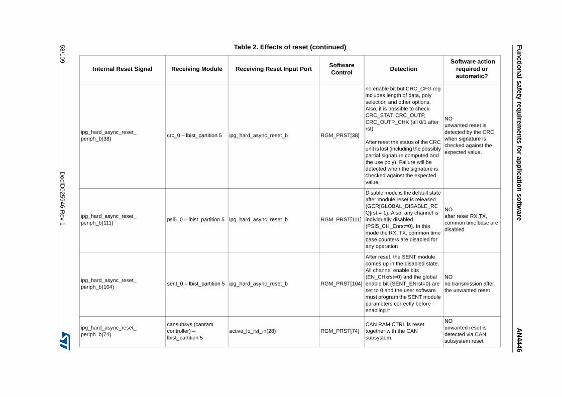
Fu
nctio
nal safety req
uirem
ents fo
r app
lication
softw
areA
N4446
58/109D
ocID025946 R
ev 1
ipg_hard_async_reset_ periph_b(38)
crc_0 – lbist_partition 5 ipg_hard_async_reset_b RGM_PRST[38]
no enable bit but CRC_CFG reg includes length of data, poly selection and other options. Also, it is possible to check CRC_STAT, CRC_OUTP, CRC_OUTP_CHK (all 0/1 after rst)
After reset the status of the CRC unit is lost (including the possibly partial signature computed and the use poly). Failure will be detected when the signature is checked against the expected value.
NOunwanted reset is detected by the CRC when signature is checked against the expected value.
ipg_hard_async_reset_ periph_b(111)
psi5_0 – lbist_partition 5 ipg_hard_async_reset_b RGM_PRST[111]
Disable mode is the default state after module reset is released (GCR[GLOBAL_DISABLE_REQ]rst = 1). Also, any channel is individually disabled (PSI5_CH_Enrst=0). In this mode the RX, TX, common time base counters are disabled for any operation
NOafter reset RX,TX, common time base are disabled
ipg_hard_async_reset_ periph_b(104)
sent_0 – lbist_partition 5 ipg_hard_async_reset_b RGM_PRST[104]
After reset, the SENT module comes up in the disabled state. All channel enable bits (EN_CHxrst=0) and the global enable bit (SENT_ENrst=0) are set to 0 and the user software must program the SENT module parameters correctly before enabling it
NOno transmission after the unwanted reset
ipg_hard_async_reset_ periph_b(74)
cansubsys (canram controller) – lbist_partition 5
active_lo_rst_in(28) RGM_PRST[74]CAN RAM CTRL is reset together with the CAN subsystem.
NOunwanted reset is detected via CAN subsystem reset
Table 2. Effects of reset (continued)
Internal Reset Signal Receiving Module Receiving Reset Input PortSoftware Control
Detection Software action
required or automatic?
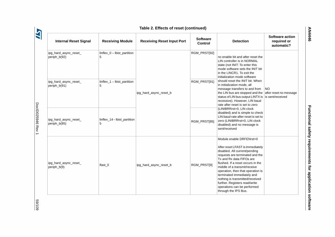
AN
4446F
un
ction
al safety requ
iremen
ts for ap
plicatio
n so
ftware
DocID
025946 Rev 1
59/109
ipg_hard_async_reset_ periph_b(92)
linflex_0 – lbist_partition 5
ipg_hard_async_reset_b
RGM_PRST[92]no enable bit and after reset the LIN controller is in NORMAL state (not INIT: To enter this mode software sets the INIT bit in the LINCR1. To exit the initialization mode software should reset the INIT bit. When in initialization mode, all message transfers to and from the LIN bus are stopped and the status of LIN bus output LINTX is recessive). However, LIN baud rate after reset is set to zero (LINIBRRrst=0, LIN clock disabled) and is simple to checkLIN baud rate after reset is set to zero (LINIBRRrst=0, LIN clock disabled) and no message is sent/received
NOafter reset no message is sent/received
ipg_hard_async_reset_ periph_b(91)
linflex_1 – lbist_partition 5
RGM_PRST[91]
ipg_hard_async_reset_ periph_b(85)
linflex_14 – lbist_partition 5
RGM_PRST[85]
ipg_hard_async_reset_ periph_b(9)
lfast_0 ipg_hard_async_reset_b RGM_PRST[9]
Module enable DRFENrst=0
After reset LFAST is immediately disabled. All current/pending requests are terminated and the Tx and Rx data FIFOs are flushed. If a reset occurs in the middle of a transmit/receive operation, then that operation is terminated immediately and nothing is transmitted/received further. Registers read/write operations can be performed through the IPS Bus.
Table 2. Effects of reset (continued)
Internal Reset Signal Receiving Module Receiving Reset Input PortSoftware Control
Detection Software action
required or automatic?
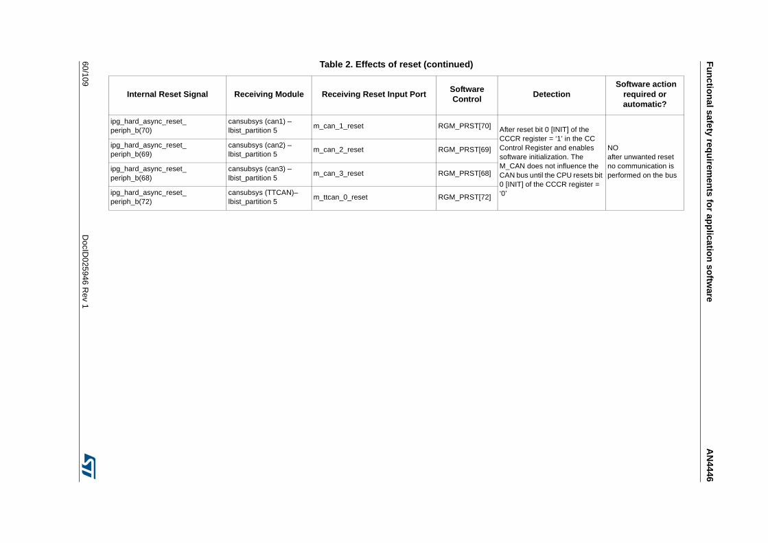
Fu
nctio
nal safety req
uirem
ents fo
r app
lication
softw
areA
N4446
60/109D
ocID025946 R
ev 1
ipg_hard_async_reset_ periph_b(70)
cansubsys (can1) – lbist_partition 5
m_can_1_reset RGM_PRST[70] After reset bit 0 [INIT] of the CCCR register = ‘1’ in the CC Control Register and enables software initialization. The M_CAN does not influence the CAN bus until the CPU resets bit 0 [INIT] of the CCCR register = ‘0’
NOafter unwanted reset no communication is performed on the bus
ipg_hard_async_reset_ periph_b(69)
cansubsys (can2) – lbist_partition 5
m_can_2_reset RGM_PRST[69]
ipg_hard_async_reset_ periph_b(68)
cansubsys (can3) – lbist_partition 5
m_can_3_reset RGM_PRST[68]
ipg_hard_async_reset_ periph_b(72)
cansubsys (TTCAN)– lbist_partition 5
m_ttcan_0_reset RGM_PRST[72]
Table 2. Effects of reset (continued)
Internal Reset Signal Receiving Module Receiving Reset Input PortSoftware Control
Detection Software action
required or automatic?
DocID025946 Rev 1 61/109
AN4446 Functional safety requirements for application software
108
3.3.15 Periodic Interrupt Timer (PIT)
If a failure in the PIT can cause the violation of a safety goal, some software mechanisms are needed to guarantee the integrity of the PIT module.
Assumption: PIT operations (for example, the number of periodic triggers) are checked and compared against the expected values every FTTI.
To implement this test, the number of interrupts generated by the PIT within a given time period shall be compared with the expected number of interrupts. To avoid CCF, the reference for the time period shall be independent from the PIT (for example, SWT).
If not covered by other means, software shall read back the PIT configuration and compare it with the expected configuration (for example, check for enabled channels and compared values, and so on.).
In all cases, when timing/latency of PIT interrupts is important, software shall check that the PIT interrupts are generated within the expected time.
3.3.16 System Timer Module (STM) usage
Assumption: Since a failure in the System Timer Module (STM) can cause a violation of the safety goal, one of the two assumptions below shall be satisfied.
Assumption: At every STM interrupt, the IRQ handler shall compare the elapsed time since the previous interrupt versus a free running counter to check whether the interrupt time is consistent with the STM setting, or
Assumption: The STM IRQ handler shall be under SWT protection.
A second timer may be used to measure STM interrupts and compare with the STM measured time.
3.3.17 I/O and Peripheral Bridge
Assumption: The integrity of safety relevant periphery will be mainly ensured by application-level measures (for example, connecting one sensor to different I/O modules, sensor validation by sensor fusion, and so on) which are enabled on the hardware level by a replication of all potentially safety-relevant I/O with appropriate freedom of interference but no hardware checkers. This replication starts at the I/O bridges (including them).
Safety relevant peripherals are assumed to be used redundantly in some way. Different approaches can be used, for example by getting replicated input, (for example, connect one sensor to two DSPIs or even connect two sensors measuring the same quantity to two ADCs) or by cross-checking some I/O operations with different operations (for example, using sensor values of different quantities to check for validity).
Recommendation: The usage of different data coding (for example, inversion) is recommended for redundant communication over safety relevant peripherals (for example, DSPI or LINFlex).
Assumption: Different data coding or message transfer timing is used for redundant communication over DSPI_4 and DSPI_5.
Users can choose the approach that better fits their needs.
To allow a safety application to make redundant use of all I/O peripherals, the peripherals have two instances and each instance is connected to a different peripheral bridge
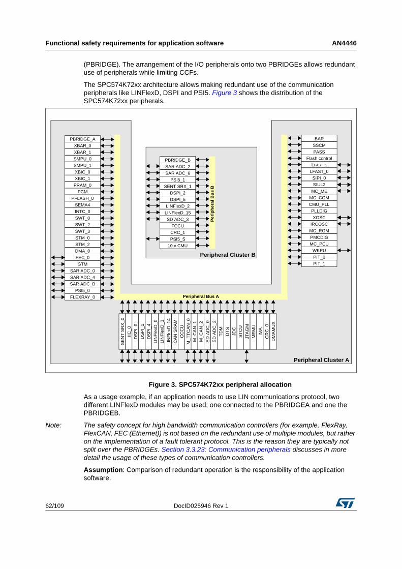
Functional safety requirements for application software AN4446
62/109 DocID025946 Rev 1
(PBRIDGE). The arrangement of the I/O peripherals onto two PBRIDGEs allows redundant use of peripherals while limiting CCFs.
The SPC574K72xx architecture allows making redundant use of the communication peripherals like LINFlexD, DSPI and PSI5. Figure 3 shows the distribution of the SPC574K72xx peripherals.
Figure 3. SPC574K72xx peripheral allocation
As a usage example, if an application needs to use LIN communications protocol, two different LINFlexD modules may be used; one connected to the PBRIDGEA and one the PBRIDGEB.
Note: The safety concept for high bandwidth communication controllers (for example, FlexRay, FlexCAN, FEC (Ethernet)) is not based on the redundant use of multiple modules, but rather on the implementation of a fault tolerant protocol. This is the reason they are typically not split over the PBRIDGEs. Section 3.3.23: Communication peripherals discusses in more detail the usage of these types of communication controllers.
Assumption: Comparison of redundant operation is the responsibility of the application software.
XBAR_1
SMPU_0
SMPU_1
XBIC_0
XBIC_1
PRAM_0
PFLASH_0
SEMA4
INTC_0
SWT_0
SWT_2
SWT_3
STM_0
STM_2
DMA_0
FEC_0
GTM
SAR ADC_0
SAR ADC_4
SAR ADC_B
PSI5_0
FLEXRAY_0
BAR
SSCM
PASS
LFAST_1
LFAST_0
SIPI_0
SIUL2
MC_ME
MC_CGM
CMU_PLL
PLLDIG
XOSC
IRCOSC
MC_RGM
PMCDIG
MC_PCU
WKPU
PIT_0
SE
NT
SR
X_0
IIC_0
DS
PI_
0
DS
PI_
1
DS
PI_
4
LIN
Fle
xD_0
LIN
Fle
xD_1
LIN
Fle
xD_1
4
CA
N S
RA
M
CC
CU
M_T
TC
AN
_0
M_C
AN
_2
SD
AD
C_0
SD
AD
C_2
TD
M
DT
S
JDC
ST
CU
JTA
GM
ME
MU
IMA
CR
C_0
DM
AM
UX
Peripheral Cluster A
Peripheral Bus A
PBRIDGE_B
SAR ADC_2
SAR ADC_6
PSI5_1
SENT SRX_1
DSPI_2
DSPI_5
LINFlexD_2
LINFlexD_15
SD ADC_3
FCCU
CRC_1
PSI5_S
Per
iph
eral
Bu
s B
Peripheral Cluster B
M_C
AN
_1
PBRIDGE_A
XBAR_0
PIT_1
Flash control
PCM
10 x CMU
DocID025946 Rev 1 63/109
AN4446 Functional safety requirements for application software
108
Note: Additional details can be found in the “I/O peripherals” section in the “Functional Safety” chapter of the SPC574K72xx Reference Manual.
There are modules, particularly on-platform peripherals as INTC and eDMA, with a single peripheral interface. For these modules, the integrity of accesses to their register interface is not guaranteed by the PBRIDGE replication, and the following assumptions are required to cover failures affecting the value of data read from or written to their register interface.
Assumption: Software periodically checks the contents of configuration registers, and more than 10 registers of modules attached to PBRIDGEn are part of the countermeasure described in Section 3.3.2: CRC of configuration registers.
Assumption: To ensure safe usage of modules which do not exist redundantly and are connected to only one PBRIDGE, one of the following shall be true for each user-visible (via the PBRIDGEn) register:
• The register is not relevant for the safety goal of the application.
• The register has a constant value (typically a configuration register) which is periodically checked for correct value (for example, by CRCing).
• Wrong values written into the register are detected by other safety measures.
Furthermore, for reading such registers the following is obviously true (due to the single nature of the data source):
• Values read from such registers are not guaranteed to be free of SPFs
Note: The FMEDA assumes that the above condition holds for at least 99% of the respective registers, but it is recommended to ensure it for 100% to reduce documentation complexities.
Assumption: Software shall read back the values written to registers of non-redundant peripherals.
Note: Not necessary for configuration registers which are under CONF_REG_CRC_SCAN (as described in SM_FMEDA_063 (on page 63))as that serves as a read-back on its own.
Assumption: When software reads a safety-relevant value from a peripheral, that value is read twice in a row, then the two read values are compared. This helps detect transient errors in the PBRIDGE for non-redundant peripherals.
3.3.18 System Integration Unit Lite (SIUL2)
Since the SIUL2 PBRIDGE interface is unique, its failure, and particularly of its register protection module, may impact redundant I/O functionalities leading to CCF.
Assumption:When the SIUL2 is used for the implementation of safety related I/O functionality, application level redundancy is such that it covers at least 60% of failures introduced by the REG_PROT module that can result in blocked writes (lost updates) to non-locked registers (mostly GPO data registers). An additional software test shall run to detect such a failure mode.
Note: A read-back after each write to the SIUL registers is sufficient to cover this failure mode.
Assumption: To detect wrong or multiple addressing failures, the startup read-back of SIUL configuration registers shall be executed after all SIUL2 registers have been written.
Assumption: If the SIUL2 is used to perform a redundant digital input or output (read two GPIs or write two GPOs), the application will execute a periodic CRC of configuration
Functional safety requirements for application software AN4446
64/109 DocID025946 Rev 1
registers that will be used to detect decoder hard faults that lead to CCF on data reads or writes.
3.3.19 GTM Wrapper
Assumption: To detect if the GTM stops running due to a fault, application software shall periodically verify the GTM is running by reading the GTM status register (GTMDI_DS).
Assumption: Application software shall check the configuration of the GTM Wrapper once per FTTI (for example, reading back the GTM configuration registers and compare them against the expected values).
Assumption: Safety analysis assumes that failures in data registers (other than configuration failures), as well as in the GTM logic, are covered by application measures.
3.3.20 External Bus Interface (EBI)
Assumption: Neither EBI nor LFAST are used in safety related applications. If used, it is the responsibility of the application software to recognize and detect failures caused by internal FIFO overflow or underflow (incorrect write or read operations), which may lead to wrong command, data or message loss.
Assumption: IRQs from the LFAST module should be disabled on the safety core to prevent faulty LFAST communication from interfering with the execution of a safety related task. If not disabled, other measures shall be implemented to detect possible IRQ flooding.
3.3.21 Reading analog inputs
Acquisition of safety related analog inputs can be performed using two independent ADCs modules redundantly.
The dual read analog input uses two analog input channels provided by two separate ADC modules to acquire a replicated analog input signal. Both ADC units acquire and digitize the two copies of a redundant analog signal connected to the inputs. In this configuration (if applied to all possible analog inputs), only half of the analog inputs are available to the applications.
Assumption: Software will read back the SIUL2 configuration once after programming to assess the correct configuration and connectivity of the two analog inputs.
Assumption: Software will compare the value sampled by the two ADCs and decide on their consistency (comparison has to take into account conversion differences and tolerances).
3.3.22 Software Watchdog Timer (SWT) usage
The objective of the Software Watchdog Timer (SWT) is to detect a defective program sequence when individual elements of a program are processed in the wrong sequence or period of time. Once the SWT is enabled, it requires periodic and timely execution of the watchdog servicing procedure. The service procedure must be performed within the configured time window, before the service timeout expires.
It is in general to be expected that software uses the software watchdog timer (SWT) to detect lost clocks or significantly slow clocks. Using the SWT to detect clock issues is a secondary measure since there are primary means for checking the clock integrity (for example, CMU).
DocID025946 Rev 1 65/109
AN4446 Functional safety requirements for application software
108
SPC574K72xx provides the hardware support (SWT) to implement both control flow and temporal monitoring methods. If Windowed mode and Keyed Service mode (two pseudorandom key values used to service the watchdog) are enabled, it is possible to reach a high effective temporal flow monitoring.
Assumption: It is the responsibility of the application software to insert the control-flow checkpoints with the required granularity according to application needs.
SWT can be configured to stop, or continue, running when the MCU is in STOP mode by configuring SWT_CR[STP]. If this SWT feature doesn't work as expected due to a fault, the safety function could be impaired (for example, SWT could trigger an unwanted reset while the device is in STOP mode).
Assumption: Current FMEDA assumes that STOP mode is not used in normal operations.
3.3.23 Communication peripherals
Assumption: Communication over the following interfaces shall be protected by a fault-tolerant communication protocol (implemented by the operating system or the application):
• FlexRay
• FlexCAN
• Ethernet
– Typically such a layer would contain an E2E CRC, a sequence counter, a sender ID and (if transmission loss needs to be prevented) an acknowledgement mechanism.
Assumption: If safety relevant, FlexRay and FlexCAN shall not be clocked directly by the XOSC.
Note: Directly using the XOSC as the source can expose the FlexRay or FlexCAN engines to glitches that would otherwise be filtered by the PLL.
Note: Customers can use the XOSC provided they implement safety mechanisms to detect the effects of glitches. These mechanisms can be part of the fault tolerant protocol.
An appropriate safety software protocol should be utilized for any communication peripheral employed to meet ASIL D application requirements
FlexRay, FlexCAN and Ethernet don’t have special safety mechanisms other than what is included into them by their protocol specs. The application software or operating system needs to provide the safety measures on top of the IP modules to meet safety requirements.
3.3.24 Temperature sensor (TSENS)
The SPC574K72xx includes an on-board temperature sensor that monitors device temperature and delivers one analog output signal and three digital output signals.
The analog output signal is internally connected to an ADC input to acquire a value which is proportional to the temperature. Starting from this value, software can measure the current device temperature.
The three digital outputs are used to signal to the device conditions of undertemperature and overtemperature.
In case of an undertemperature or overtemperature event two detection paths are implemented, one via the digital output and one via the analog output. The analog path
Functional safety requirements for application software AN4446
66/109 DocID025946 Rev 1
requires some software steps (for example, acquiring the value and applying a formula to obtain the temperature).
Assumption: Software shall read the analog output of the temperature sensor via the ADC and check for temperature violations at least once per FTTI.
Note: If only the analog output indicates undertemperature or overtemperature (but no digital indication), a TSENS failure might be indicated.
3.3.25 Analog to Digital Converters
The basic idea to verify the integrity of the functional ADCs is to implement software redundancy. This redundancy is supported by the hardware which allows acquiring analog inputs using independent ADC modules(j).
To decrease the probability of common cause of failure supervisor ADC and functional one don't share the same analog multiplexer.
Assumption: Analog inputs, which are safety relevant, shall be acquired redundantly by the functional and supervisor ADCs. The acquired values shall be compared by software.(k)
Note: Other types of redundancy can be implemented at application level. For example, information can be acquired redundantly by the MCU using analog data, i.e. via ADC, and digital data, i.e. via a communication protocol. Choosing the best strategy depends on the application.
This assumption is the main measure to be implemented. Some additional measures have been considered during the safety analysis to guarantee the integrity of all modules involved with the analog acquisition.
The SD ADC is expected to convert fast signals. The redundant acquisitions may not be effective if the frequency of the input analog signal is too high compared to conversion time and the time between the 2 redundant acquisitions. In such a case other mechanisms can be implemented, for example plausibility checks.
Assumption: In case analog input signal is expected to have certain dynamic/transient characteristics which make the redundant acquisition ineffective, the acquired data shall analyzed for such characteristics to verify the plausibility of the conversion.
Note: This measure mainly applies on the SDADC which is supposed to convert fast signals. User is expected to implement such a mechanism whether the redundant acquisition is not effective, for example due to the dynamic of the input signal.
An example of this mechanism is to verify if the FFT of the input signal is compatible with the expected one.
Assumption: Software periodically checks the contents of configuration registers of ADCs to ensure that the configuration has not accidentally changed.
Note: This counter-measure is part of the one described in Section 3.3.2, CRC of configuration registers.
j. Simultaneous sampling of two ADCs on the same analog input is not allowed (see the SPC574K72xx Reference Manual for details).
k. Functional and supervisor ADCs share the same bias; a specific software mechanism to detect failures affecting the bias is presented (for example, SELFTEST_SARB_FTTI).
DocID025946 Rev 1 67/109
AN4446 Functional safety requirements for application software
108
ADCs embed an analog watchdog mechanism to trigger automatically DMA/interrupt request in case the converted value is outside configurable thresholds. The integrity of this hardware mechanism and the proper generation of DMA and interrupt from ADC can be verified by software.
Assumption: Once every FTTI, The ADC shall trigger a DMA/interrupt request by manipulating the thresholds of the analog watchdog with respect to a reference conversion.
Note: This safety mechanism doesn't cover the analog watchdog only, but it verifies the integrity of the interrupt and DMA generation by the ADC module. This procedure is required to run even if the analog watchdog is not used by the safety application.
Assumption: Every trigger (either hardware or software), which starts a conversion sequence, also initiates a timer or watchdog to monitor the conversion sequence duration.
Note: In case conversion time exceeds the expected value, this timer or watchdog shall abort the corresponding ADC conversion.
In case of scan mode, the conversion time is monitored for duration deviation more than the conversion time of a single channel.
Assumption: At the end of the conversion of all enabled channels (or after a CONV_TIME_MON time-out), software shall check the status of the conversion to detect any missed or spurious request. The status of the last conversion shall be cleared before starting a new one.
Note: In case of SAR ADC some registers which give information about the status of the conversion are showed below:
VALID and OVERW flags of the CDR registers
EOC/ECH flags
ECAWORRx (or ICAWOOR) and WTISR to verify any violation triggered by the analog watchdog.
Note: In case of SDADC the register showing status information is the SFR.
Note: Please check section on the SDADC of the reference manual to have all details.
Assumption: In case the DMA is used to transfer the converted data from ADC modules to the memory, at the end of the conversion of all enabled channel VALID and OVERW flags of the CDR register and EOC status flags are verified against programmed configuration of DMA to detect any missing or spurious request.
Functional and supervisor ADCs share the same reference bias. Since a failure affecting the bias can cause the violation of the safety goal, its integrity shall be verified at least per FTTI. This check can be done via software by acquiring some known analog values via the supervisor ADC.
Assumption: At least once per FTTI, the supervisor ADC shall acquire some known internal analog voltage signals and compare them with the expected values before being used to monitor the functional ADCs.
Note: The implementation of this software mechanism is the same than the SELFTEST_SARB one. The only difference is the execution frequency.
3.3.26 Mode Entry (MC_ME)
The SPC574K72xx can be configured in different functional modes. Each mode has its own unique configuration (for example, enabled peripherals and clock).
Functional safety requirements for application software AN4446
68/109 DocID025946 Rev 1
The mode configurations and the transition between different modes is controlled by the MC_ME. The correct execution of a mode transition shall be verified by application software.
Assumption: After the mode transition request, application software shall verify the status of the transition within the expected completion delay. Also, the new configuration is compared with the intended configuration. Completion delay is always monitored while the status check is performed, unless the target mode is low-power.
Assumption: Mode transition process duration, from transition request to transition complete, shall be monitored.
3.3.27 Semaphores (SEMA42)
Semaphores embedded in the SPC574K72xx is robust hardware support for implementing a simple mechanism to achieve “lock/unlock” operation of shared resources.
Assumption: To verify the integrity of the semaphores logic, application software before locking (or unlocking) a gate, shall check that the value of the gate is the expected one.
Note: Checking the gate state after the locking (or unlocking) request verifies if the gate has been properly locked (or unlocked).
Checking before unlocking the gate helps detect if other masters erroneously received the lock before it was released by the current master.
Checking before locking helps detect if the gate is already erroneously assigned to the requesting master.
3.4 Operational interference protectionAs a multi-master system, the SPC574K72xx provides safety mechanisms to prevent non-safety masters from interfering with the operation of the safety core, as well as mechanisms to handle the concurrent operation of software tasks with different or lower ASIL.
3.4.1 Core Memory Protection Unit (CMPU)
The Core Memory Protection Unit (CMPU) ensures inter-task interference protection by providing the capability of protecting regions of memory from access by software tasks with different privilege levels. The CMPU features a 24-entry region descriptor table that defines memory regions and their associated access rights. Only accesses with the sufficient rights are allowed to complete.
Using pre-defined region descriptors that define memory spaces and their associated access rights, the CMPU concurrently monitors Core initiated memory accesses and evaluates the appropriateness of each transfer.
Assumption: The application software shall configure the CMPU (at least of the Safety core) to define the location, size, access permissions and memory attributes for each memory region that needs to be protected.
Recommendation: For ASIL D applications, the CMPU should be used to ensure that only authorized software tasks can configure modules and can access only their allocated resources according to their access rights.
DocID025946 Rev 1 69/109
AN4446 Functional safety requirements for application software
108
3.4.2 System Memory Protection Unit (SMPU)
The System MPU (SMPU) provides memory protection at the crossbar (XBAR). The SMPU splits the physical memory into 16 different regions. Each XBAR master (Core, DMA, FlexRay, SIPI) can be assigned different access rights to each region.
Assumption: The SMPU will be used to prevent non-safety masters (all except the Safety core) from accessing restricted memory regions unless those regions are similarly protected by mechanisms shown in Section 3.4.3: AIPS protection mechanism or Section 3.4.4: Register protection (REG_PROT).
Assumption: The SMPU shall only be programmed by the Safety core. This software shall prevent write accesses to the SMPU’s registers from all other masters.
Note: See “System Memory Protection Unit (SMPU)” chapter in the SPC574K72xx Reference Manual for details.
3.4.3 AIPS protection mechanism
The peripheral bridges (PBRIDGEn) translate accesses on the switched AMBA bus (XBAR) to point-to-point accesses to the majority of peripherals on the SPC574K72xx. The peripherals connected to the PBRIDGEs are PBRIDGE slaves.
The PBRIDGEs implement an additional protection mechanism to support the requirement that non-safety relevant masters and safety relevant masters do not interfere with one another. The protection mechanism allows for protection of each slave from master accesses (for example, read/write or supervisor/user access).
Assumption: The application software will configure the PBRIDGEs to define the access permissions for each slave module that requires access protection, unless protected by the mechanisms in sections Section 3.4.2: System Memory Protection Unit (SMPU) or Section 3.4.4: Register protection (REG_PROT).
PBRIDGEn should be configured to prevent any write access to the entire MC_RGM address space for all masters except the safety core.
Assumption: Safety software shall program the Peripheral Access Control in the PBRIDGEn so no write access to the MC_RGM_PRST[n] (individual module reset programming model) is allowed to access other cores.
3.4.4 Register protection (REG_PROT)
Accidental writes to configuration registers can affect the execution of the MCU’s safety function and disable the safety mechanism due to their change. Register protection offers a mechanism to protect defined memory mapped address locations in a module against writes. The address locations that can be protected are module specific.
Register protection includes these distinctive features:
• Register protection restricts write accesses for the module under protection to supervisor mode only. This access restriction is in addition to any access restrictions imposed by the protected module.
• A register cannot be written once Soft Lock Protection is set. Soft Lock Protection can be cleared by software or system reset.
• A register cannot be written once Hard Lock Protection is set. Hard Lock Protection can only be cleared by system reset.
Functional safety requirements for application software AN4446
70/109 DocID025946 Rev 1
Recommendation: It is recommended that only hardware related software (OS, drivers) run in supervisor mode.
Assumption: For ASIL D applications, all configuration registers, and registers that aren’t modified during application execution, shall be protected with a Hard Lock Protection. Configuration registers, and registers which have limited writes every trip time, shall be protected with soft-lock protection.
Assumption: Configuration registers are to be locked 90% of the time, either by Soft Lock or Hard Lock Protection, to prevent unwanted modifications.
Note: Implementation hint: Most of the off-platform peripherals have their own REG_PROT. Each peripheral that can be protected through the REG_PROT has a Set Soft Lock bit in the Register Protection space. This bit should be asserted to enable the protection of the related peripheral.
Note: Each peripheral register that can be protected through register protection has a Set Soft Lock bit reserved in the Register Protection address space. This bit should be asserted to enable the protection of the related peripheral registers. Moreover, the Hard Lock Bit (REG_PROT_GCR[HLB] = 1) should be set for best write protection.
Assumption: The REG_PROT configuration registers shall be read and compared against the expected values at least once after being programmed.
3.4.5 Peripheral Core (Core_2)
Peripheral (Core_2) core is considered Non-safety modules (NoSaMo). If it executesany safety task, counter measures must be used in application software.
Some hardware resources are shared between Core_2 and the Safety core (master and checker cores).
Assumption: No more than 20% of the entire address space contains writable safety-relevant modules or data.
Assumption: To avoid excessive accesses to shared resources the NoSaMo core (Core2) has lower XBAR priority than the safety core (Master core and Checker core).
Assumption: The local memories of the NoSaMo core must not be used to store safety-relevant data, or only if software protection against spurious changes by the NoSaMo core exists.
Assumption: To avoid unwanted software interrupts triggered by the Peripheral core (Core_2) which is handled by the safety core, one of the following holds:
• Accidental access to the triggering registers of these interrupts is prevented (typically by SMPU and/or AIPS_PACR)
• There exists an additional indicator (in addition to the triggering register, for example, a variable in RAM) which can be used to execute an ISR_CHECK_TRIGGER_SET (on page 41) like functionality.
Alternatively, the safety core could be configured to ignore software triggered interrupts.
Assumption: Safety-relevant software will enable the INTC_MPROT lock bit.
DocID025946 Rev 1 71/109
AN4446 Functions of external devices for ASIL D applications
108
4 Functions of external devices for ASIL D applications
This section describes the external components needed to use with SPC574K72xx in a system for ASIL D applications. It is assumed that the system reacts safely to SPC574K72xx being in or entering all Safe stateMCU.
It should be noted that the failure rates of external services are not included in the FMEDA of SPC574K72xx and have to be included in the system FMEDA by the user himself.
4.1 External reset outputSPC574K72xx has pin named external reset output (ESR0). The signal on this pin can be used as input to one, or more, external devices. It is possible that an unwanted or spurious assertion of ESR0 may not be detected by the SPC574K72xx. This could cause the external device to get reset without any automatic detection by SPC574K72xx. Assumption is that countermeasures against this failure mode must be considered at system level.
Assumption: System level I/O safety measures have at least 99% DC against joint spurious reset of all external devices.
4.2 High impedance outputsSystem-level countermeasures have to be placed in order to bring the safety-critical outputs to their safe state (for example, by pull-up or pull-down resistors) when an output high-impedance is not considered safe. Normally this requirement will be fulfilled by ensuring the error out pin(s) are pulled to the failure state. Additionally, users may drive pins (for example, CAN Tx pins) to levels that prevent interference with other parts of the system that are assumed to be independent.
Assumption: If a high impedance state on an output pin is not safe, pull-up or pull-down resistors need to be added to outputs that are safety-critical depending on application requirements for the SPC574K72xx during unpowered or reset conditions.
4.3 External Watchdog (EXWD)An external device, acting as supervisor of the operations, must provide a watchdog to cover common-cause failures of SPC574K72xx for ASIL D applications.
Assumption: An external watchdog shall exist to detect failures completely disabling the SPC574K72xx, including its safety mechanisms.
The external watchdog will detect CCFs, such as failure of the power supply. If a failure is detected, the external watchdog should move the system to a Safe statesystem within the FTTI.
Assumption: The EXWD shall be triggered periodically, either by the software providing the safety function on the SPC574K72xx or by a toggling protocol on the error output pin(s).
Implementation of the watchdog communication between SPC574K72xx and the external device is up to the user (for example, communication via serial link, ethernet, via toggling pin, or via the FCCU error out signals).
Functions of external devices for ASIL D applications AN4446
72/109 DocID025946 Rev 1
Assumption: To avoid undetected reset cycling under rare circumstances the external watchdog will not be reset by the MCU reset output.
Note: There must be a signalling path from the safety software to the external system through which the software can confirm correct initialization. This is not automatically guaranteed by the FI[n] signals which communicate the status of the device independently from software. On the other hand, a different communications interface (such as a serial link) can be used to detect incorrect software initialization.
4.4 Power supplyAssumption: The device has been developed with the assumption that an external power supply of appropriate voltage shall be supplied (see the SPC574K72xx Data Sheet’s for operating voltage specifications). All internal and external supplies are considered safety critical and shall be monitored for deviations beyond predefined thresholds.
Assumption: External power supply shall be supervised for high and low voltage deviations as shown in Table 3. Required monitors for each power supply can be found in column “External monitor required”.
Note: Voltage monitors are provided on the SPC574K72xx to monitor the internal supplies of the device. See table “POR and voltage monitors description” in the “Power management” chapter of the SPC574K72xx Reference Manual for a list of monitored supplies.
Note: LVD/HVD are necessary to ensure logic functionality. External LVD can be removed if the failure can be detected by other means, but the external HVD is necessary to prevent physical damage.
Assumption: External supervision shall hold the SPC574K72xx in a Safe stateMCU and the system in its Safe statesystem if the external voltage is outside specifications. The MCU shall be protected against voltages over the maximum survivable level of the technology.
Recommendation: It is recommended to protect the MCU against voltage above the maximum survivable level of the technology (for example, using a Zener diode) to prevent destruction of the MCU.
Note: See the SPC574K72xx Data Sheet’s “Absolute maximum ratings” and “DC electrical specifications” sections for power supplies requirements.
The SPC574K72xx embeds two types of voltage supervisors, Low Voltage Detect (LVD) and High Voltage Detect (HVD) monitors. Safety relevant voltages are supervised for
Table 3. SPC574K72xx required external monitors
Name Description External Monitor Required
VDD_HV_ADR_D Voltage reference of ADC sigma/delta module LVD/HVD
VDD_HV_ADR_S Voltage reference of ADC SAR module LVD/HVD
VDD_HV_IO_MAIN High voltage Power supply for the I/O’s HVD
VDD_HV_ADV High voltage supply for the ADC modules HVD
VDD_HV_FLA Decoupling supply pin for Flash HVD
VDD_HV_IO_FLEX FlexRay/Ethernet 3.3 V I/O supply HVD
VDD_HV_IO_JTAG JTAG_I/O pin supply HVD
DocID025946 Rev 1 73/109
AN4446 Functions of external devices for ASIL D applications
108
voltages that are out of these ranges. Since safety relevant voltages have the potential to disable the failure indication mechanisms of the SPC574K72xx (such as FCCU, Pads, and so on) their error indication directly causes a transition into the Safe stateMCU (for example, reset assertion).
Some LVDs and HVDs are configurable and enabled by default. Application should not disable safety relevant LVDs or HVDs. See the “POR and voltage monitors description” table in the “Power management” chapter of the SPC574K72xx Reference Manual for the list of configurable LVDs and HVDs.
4.5 Error Out Monitor (ERRM)The FCCU has two external pins: FI[0] and FI[1]. An external device must be connected to the FCCU via FI[0] and optionally FI[1] to continually monitor the error output pins of the FCCU.
Assumption: The overall system needs to include measures to monitor the error output pin(s) of the SPC574K72xx and move the system into a Safe statesystem when an error is indicated.
Assumption: If the SPC574K72xx is signalling a failure via its error output pin(s), other output pins can not be relied on.
4.5.1 Both FCCU pins connected to external device
Depending on user selection, there are two different ways to interface to the FCCU:
• Both FCCU pins connected to the external device
• Only a single FCCU pin connected to the external device
The user can choose between these two FCCU configurations, depending on which best fits the hardware and software system.
Assumption: If both error out pins are connected to the external device, the external device itself shall check both signals, taking into account the behavior of the two pins as defined in Table 4.
In this configuration the external device continuously monitors the output of the FCCU. Thus it can detect if the error out pins are not working properly. The advantage of the two pin configuration with respect to the single pin option is that it does not require any dedicated software.
Table 4. FCCU EOUT pin behavior(1)
2-pin protocol FI[1] FI[0] Definition of faulty state
Bi-stable 1 0 Two pins are out of phase and FI[0] is low
Time switching 1 0 Two pins are out of phase and FI[0] is low
Dual rail toggle_inv toggle_inv Tow pins are not out of phase
Dual rail 1 toggle_inv Two pins are not out of phase
1. See “EOUT interface” section in the “Fault Collection and Control Unit (FCCU)” chapter of the SPC574K72xx Reference Manual for details. If Error phase is accompanied by a functional reset, FI[1]/EOUT1 becomes high-z with weak pull-up, while FI[0]/EOUT0 behaves as described.
Functions of external devices for ASIL D applications AN4446
74/109 DocID025946 Rev 1
Note: Implementation hint: Monitoring the error output pins through a combinatorial logic (for example, XOR port) can generate some glitches. Oversampling these pins reduces the possibility that the glitches occur. A functional reset has no affect on FI[0], but it sets FI[1] to high-impedance with a pull-up. To avoid changing FI[1] during a functional reset when time-switching or bistable protocol is used, it is recommended to configure FCCU_CFG[PS] = 0.
4.5.2 Single FCCU pin connected to external device
In this configuration, only the FI[0] pin is connected to the external device. If a fault occurs, the FCCU communicates it to the external device through the FI[0] pin.
The functionality of FI[0] can be verified in two ways on a system level by testing that FI[0] can trigger the Safe statesystem. If only FI[0] needs to be tested (without the rest of the shutdown path), this can be accomplished with either of the following:
• FI[0] output, and FI[0] input (loop through the IO pad).
• FI[0] output connected externally to a normal GPIO.
The customer must choose which solution best fits their requirement.
Assumption: After boot, but before executing the safety function, the functionality of FI[0] pin shall be verified(l).
As access to FI[0] is shared between the FCCU and GPIO there is a failure mode where the multiplexing fails and FI[0] becomes controlled by GPIO. To make this detectable, the respective GPIO needs to be configured to drive FI[0] into the fail state.
Assumption: If an error indication protocol is selected which makes use of only one error out pin (for example, FI[0]), then SW configures any I/O MUXed to that pin to drive low before switching the pin to FCCU control (see the SPC574K72xx Reference Manual’s “Signal Description” chapter and the “I/O Signal Description table” for pin MUXing specifics).
The advantage of this configuration with respect to the configuration where two error indication signals are used, is that it can use an external device that does not compare the two signals.
Assumption: If the system is using the SPC574K72xx in a single error output pin mode, the application software shall configure the pins and pads neighboring the FI[0] to use a lower drive strength.
Using a lower drive strength on the pins near FI[0] will reduce the effects of simultaneously switching outputs on signal integrity. Software must configure the slew rate for the relevant pads in the Pad Configuration Register.
l. Since FCCU is a monitor, it is sufficient to verify the FI[0] signal only at start-up in order to avoid latent faults.
DocID025946 Rev 1 75/109
AN4446 Address decoding coverage
108
5 Address decoding coverage
5.1 Overview The MPC574xx/SPC57xxxx embeds a hardware mechanism called Single Bit Error Correction and Dual Bit Error Detection(m) to detect and, if possible, to correct failures impacting the RAM array. This hardware measure is based on a modified Hamming code algorithm.
Faults impacting the addressing logic, i.e. addressing faults, cause in general Multi Bit Errors (MBEs). The MPC574xx/SPC57xxxx does not embed a specific hardware mechanism to manage this type of faults, but these MBEs can be interpreted by the modified Hamming code algorithm as Single Bit Errors (SBEs).
The probability that an MBE results in an ECC hit is fairly high. In this case the ECC/EDC hardware “wrongly” interprets an MBE as SBE. This may cause a violation of the safety goal.
This chapter explains how, in case of ECC hit, a software test can differentiate between a SBE and a MBE due to a permanent fault in the addressing logic.
5.2 Test implementationBasic mechanism behind addressing fault detection is the ECC with address contribution embedded in the MPC574xx/SPC57xxxx devices.
Reading from locations affected by permanent addressing faults returns a random pattern. The diagnostic coverage (DC) of the ECC against addressing faults on a single access is about 70%.
To improve this DC, the idea is to perform multiple memory reads in order to trigger the failure mechanism multiple times, say K, and in multiple locations. In such a way the overall DC increases up to DC=1-(1-70%)K.
This formula is valid under the assumption that the K failures are somehow independent. It is thus fundamental:
understanding how to trigger K independent failures in case of addressing fault, and
minimizing the number of memory operations, say M, necessary to trigger the K failures.
The described algorithm is focused on the detection of failures affecting RAM address decoder considering both rows and columns of the array.
To achieve these objectives, user shall know the “hit address”(n) and details on how the memory is implemented.
m. These mechanisms are also known as ECC/EDC or SEC/DED
n. “Hit address” is the address where a single bit error correction occurs
Ad
dress d
ecod
ing
coverag
eA
N4446
76/109D
ocID025946 R
ev 1
Table 5. List of RAMs for self-test
Word Address Pre-decoding bits
Row SelectionColumn
Selection
Location MemoryShall be tested?
Mux # WordsBits per words
N bit address
Dec D Dec C Dec B Dec A Dec EBlock
Address
Core_0 (Safety Core) I-Mem yes 8 2048 72 13 A<12> A<11:9> A<8:6> A<5:3> A<2:0>
D-Mem0(1) yes 8 8192 40 13 A<12> A<11:9> A<8:6> A<5:3> A<2:0>
D-Mem11 yes 8 8192 40 13 A<12> A<11:9> A<8:6> A<5:3> A<2:0>
FlexRay DRAM not mandatoryapplication dependent
4 128 26 10 A<9:7> A<6:4> A<3:2> A<1:0>
LRAM not mandatoryapplication dependent
4 96 126 12 A<11> A<10:8> A<7:5> A<4:3> A<2:0>
GTM FIFO not mandatoryapplication dependent
8 1024 36 12 A<11:9> A<8:7> A<6:5> A<4:3> A<2:0>
(MCSi)-RAM0, i=0-2
not mandatoryapplication dependent
8 1024 39 12 A<11:9> A<8:7> A<6:5> A<4:3> A<2:0>
(MCSi)-RAM1, i=0-2
not mandatoryapplication dependent
8 512 39 12 A<11:9> A<8:7> A<6:5> A<4:3> A<2:0>
AN
4446A
dd
ress deco
din
g co
verage
DocID
025946 Rev 1
77/109
DPLL-1A not mandatoryapplication dependent
4 128 31 10 A<9:7> A<6:4> A<3:2> A<1:0>
DPLL-1B not mandatoryapplication dependent
4 384 31 10 A<9:7> A<6:4> A<3:2> A<1:0>
DPLL-2 not mandatoryapplication dependent
8 1024 31 12 A<11:9> A<8:7> A<6:5> A<4:3> A<2:0>
TTCAN TTCAN not mandatoryapplication dependent
8 3008 39 12 A<11:9> A<8:7> A<6:5> A<4:3> A<2:0>
NAR NAR(0,1,2,3) not mandatoryapplication dependent
4 64 128 12 A<11> A<10:8> A<7:5> A<4:3> A<2:0>
Platform DMA not mandatoryapplication dependent
4 128 26 10 A<9:7> A<6:4> A<3:2> A<1:0>
Platform Overlay yes 8 1024 72 13 A<12> A<11:9> A<8:6> A<5:3> A<2:0>
Table 5. List of RAMs for self-test (continued)
Word Address Pre-decoding bits
Row SelectionColumn
Selection
Location MemoryShall be tested?
Mux # WordsBits per words
N bit address
Dec D Dec C Dec B Dec A Dec EBlock
Address
Ad
dress d
ecod
ing
coverag
eA
N4446
78/109D
ocID025946 R
ev 1
Platform SRAM yes 8 8192 72 13 A<12> A<11:9> A<8:6> A<5:3> A<2:0>
Platform MPFLASH not mandatoryapplication dependent
8 1024 72 13 A<12> A<11:9> A<8:6> A<5:3> A<2:0>
Platform FEC/FICO not mandatoryapplication dependent
4 128 44 10 A<9:7> A<6:4> A<3:2> A<1:0>
Platform FEC/MIB not mandatoryapplication dependent
4 64 40 10 A<9:7> A<6:4> A<3:2> A<1:0>
1. Internal data memory of Core_0 (and Core_1) is implemented by 2 separated memory instantiations, i.e. D-Mem0 and D-Mem1. Such memories are connected in parallel. Considering a 64bit word, the first 32bit are located in D-Mem0 and the second 32bit in D-Mem1. Each memory has its own decoding logic. In case of single bit error correction, the self-test to detect failure in the addressing logic shall be executed only in the memory in which the error is detected, either D-Mem0 or D-Mem1.
Table 5. List of RAMs for self-test (continued)
Word Address Pre-decoding bits
Row SelectionColumn
Selection
Location MemoryShall be tested?
Mux # WordsBits per words
N bit address
Dec D Dec C Dec B Dec A Dec EBlock
Address

DocID025946 Rev 1 79/109
AN4446 Address decoding coverage
108
Table 5 reports multiple details about the design of each RAM impacted by the described software self-test. Details below must be used to implement the testing algorithm:
1. Muxing
2. Number of words for the whole array
3. Bits per words
4. Number of address bits
a) number of bits used as address by the RAM
5. Info ab out decoder addressing structure in terms of multiplexer
a) testing algorithm is based on several reading of different RAM locations; list of these locations depends on the decoding structure of the RAM.
During each access operation out of the memory, the word is selected via multiple decoders connected to the RAM cells. How to address bus is decoded to the memory array depends on the design parameters described in the table above.
The address bus is partitioned to:
1. row decoders (i.e. DecD, DecC, DecB and DecA)
a) these bits are used to select the row to be accessed
2. column decoders (i.e. DecA)
a) these bits are used to select the column to be accessed
3. block selection (i.e. block address)
a) these bits are used to select the block to be accessed in case the memory is internally partitioned in multiple blocks.
Let’s assume a permanent failure in the addressing logic which causes an MBE. This MBE may be “wrongly” interpreted as single bit error by the ECC/EDC hardware. The address of the reported single bit error is indicated as Ah(o).
To discriminate this permanent addressing fault from a single bit error, some back to back reads from Ah and their coupled addresses shall be executed.
Considering the hit address as starting point, the self-test requires reading a list of locations “correlated” in some way to hit address.
This list includes different locations whose address is obtained by changing one by one the bits of each decoding group (DecD, DecC and so on…).
All these memory locations shall be read following a specific order as described below.
Table 6 reports an example of list of addresses obtained starting from a specific hit address (also called victim).
o. Hitting address.
Address decoding coverage AN4446
80/109 DocID025946 Rev 1
This example assumes a single bit error reported at the hit address Ah of the SRAM. With reference to Table 5, the addressing logic of the system RAM consists of 13 bits which go through multiple decoders:
• Row selection
– DecD - A<12:10>
– DecC - A<9:8>
– DecB - A<7:6>
– DecA – A<5:4>
• Column selection
– DecE - A<3:0>
Having these parameters in mind the user, starting from the victim address, shall build a list of the locations which shall be read by the self-test.
For this example the list of locations to be read is shown on Table 6. All locations in grey shall be read. Some locations have an associated number; this number is the read order. Location #1 shall be read first, location #2 second, and so on. The order is not important for location without any number specified.
In such example the SRAM locations to be read are:
1. 0b100.01.00.11.110
2. 0b011.10.11.00.110
3. 0b011.10.11.00.001
4. and so on.
Next section describes how to compile such a list.

DocID025946 Rev 1 81/109
AN4446 Address decoding coverage
108
5.3 How to obtain the list of locations to be readThis section describes, with an example, the different steps to get the list of location to be read. The procedure starts when a single bit error correction at certain address, i.e. victim address, is reported.
Let assume the victim address is the address 0b011101100001 in the SRAM.
First step is to split the victim address in “bit grouping” depending on the decoding structure of the memory (see Table 5).
Figure 4 shows the bit grouping for the victim address of the example.
Figure 4. Bit grouping of the victim address considering the SRAM
Table 6. Example of back-to-back read to implement the test
DecE
DecD DecC DecB DecA 000 001 010 011 100 101 110 111 Description
000 10 11 00 DecD combination
001 10 11 00 DecD combination
010 10 11 00 DecD combination
011 10 01 00 DecB combination
011 10 10 00 DecB combination
011 00 11 00 DecC combination
011 01 11 00 DecC combination
011 10 11 00 6 4 10 14 16 12 2 7 Ah: victim address (red cell)
011 11 11 00 DecC combination
011 10 11 01 DecA combination
011 10 11 10 DecA combination
011 10 11 11 DecA combination
100 01 00 11 5 3 9 13 15 11 1 7 complementary address
100 10 11 00 DecD combination
101 10 11 00 DecD combination
110 10 11 00 DecD combination
111 10 11 00 DecD combination
DecD DecC DecB DecA DecE
011 10 11 00 001
row selection columnselection
Victim address Ah
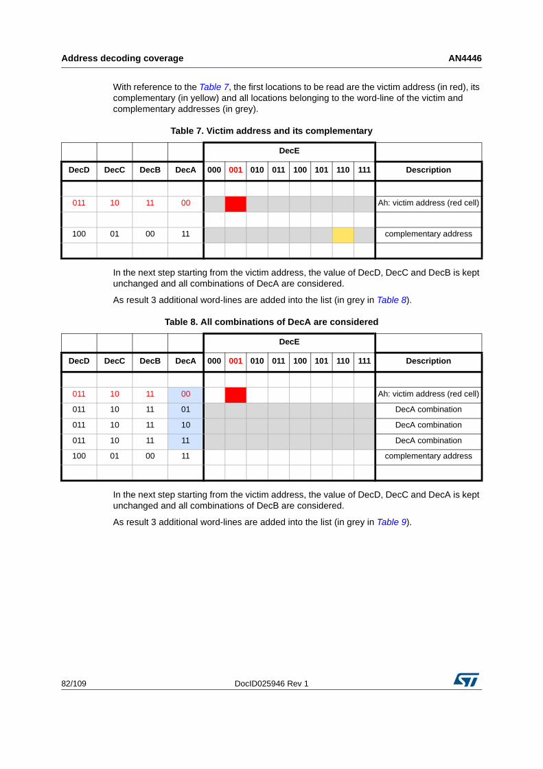
Address decoding coverage AN4446
82/109 DocID025946 Rev 1
With reference to the Table 7, the first locations to be read are the victim address (in red), its complementary (in yellow) and all locations belonging to the word-line of the victim and complementary addresses (in grey).
In the next step starting from the victim address, the value of DecD, DecC and DecB is kept unchanged and all combinations of DecA are considered.
As result 3 additional word-lines are added into the list (in grey in Table 8).
In the next step starting from the victim address, the value of DecD, DecC and DecA is kept unchanged and all combinations of DecB are considered.
As result 3 additional word-lines are added into the list (in grey in Table 9).
Table 7. Victim address and its complementary
DecE
DecD DecC DecB DecA 000 001 010 011 100 101 110 111 Description
011 10 11 00 Ah: victim address (red cell)
100 01 00 11 complementary address
Table 8. All combinations of DecA are considered
DecE
DecD DecC DecB DecA 000 001 010 011 100 101 110 111 Description
011 10 11 00 Ah: victim address (red cell)
011 10 11 01 DecA combination
011 10 11 10 DecA combination
011 10 11 11 DecA combination
100 01 00 11 complementary address
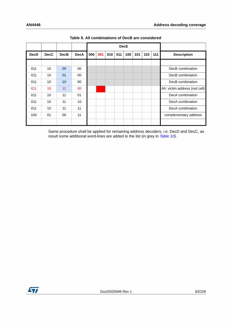
DocID025946 Rev 1 83/109
AN4446 Address decoding coverage
108
Same procedure shall be applied for remaining address decoders, i.e. DecD and DecC, as result some additional word-lines are added to the list (in grey in Table 10).
Table 9. All combinations of DecB are considered
DecE
DecD DecC DecB DecA 000 001 010 011 100 101 110 111 Description
011 10 00 00 DecB combination
011 10 01 00 DecB combination
011 10 10 00 DecB combination
011 10 11 00 Ah: victim address (red cell)
011 10 11 01 DecA combination
011 10 11 10 DecA combination
011 10 11 11 DecA combination
100 01 00 11 complementary address
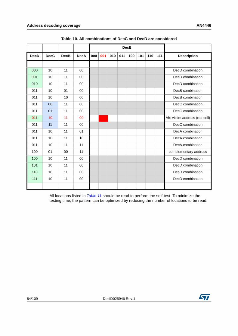
Address decoding coverage AN4446
84/109 DocID025946 Rev 1
All locations listed in Table 11 should be read to perform the self-test. To minimize the testing time, the pattern can be optimized by reducing the number of locations to be read.
Table 10. All combinations of DecC and DecD are considered
DecE
DecD DecC DecB DecA 000 001 010 011 100 101 110 111 Description
000 10 11 00 DecD combination
001 10 11 00 DecD combination
010 10 11 00 DecD combination
011 10 01 00 DecB combination
011 10 10 00 DecB combination
011 00 11 00 DecC combination
011 01 11 00 DecC combination
011 10 11 00 Ah: victim address (red cell)
011 11 11 00 DecC combination
011 10 11 01 DecA combination
011 10 11 10 DecA combination
011 10 11 11 DecA combination
100 01 00 11 complementary address
100 10 11 00 DecD combination
101 10 11 00 DecD combination
110 10 11 00 DecD combination
111 10 11 00 DecD combination
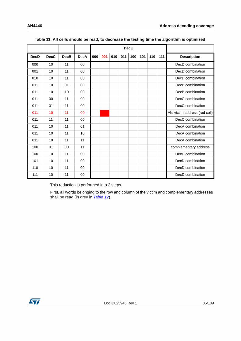
DocID025946 Rev 1 85/109
AN4446 Address decoding coverage
108
This reduction is performed into 2 steps.
First, all words belonging to the row and column of the victim and complementary addresses shall be read (in grey in Table 12).
Table 11. All cells should be read; to decrease the testing time the algorithm is optimized
DecE
DecD DecC DecB DecA 000 001 010 011 100 101 110 111 Description
000 10 11 00 DecD combination
001 10 11 00 DecD combination
010 10 11 00 DecD combination
011 10 01 00 DecB combination
011 10 10 00 DecB combination
011 00 11 00 DecC combination
011 01 11 00 DecC combination
011 10 11 00 Ah: victim address (red cell)
011 11 11 00 DecC combination
011 10 11 01 DecA combination
011 10 11 10 DecA combination
011 10 11 11 DecA combination
100 01 00 11 complementary address
100 10 11 00 DecD combination
101 10 11 00 DecD combination
110 10 11 00 DecD combination
111 10 11 00 DecD combination
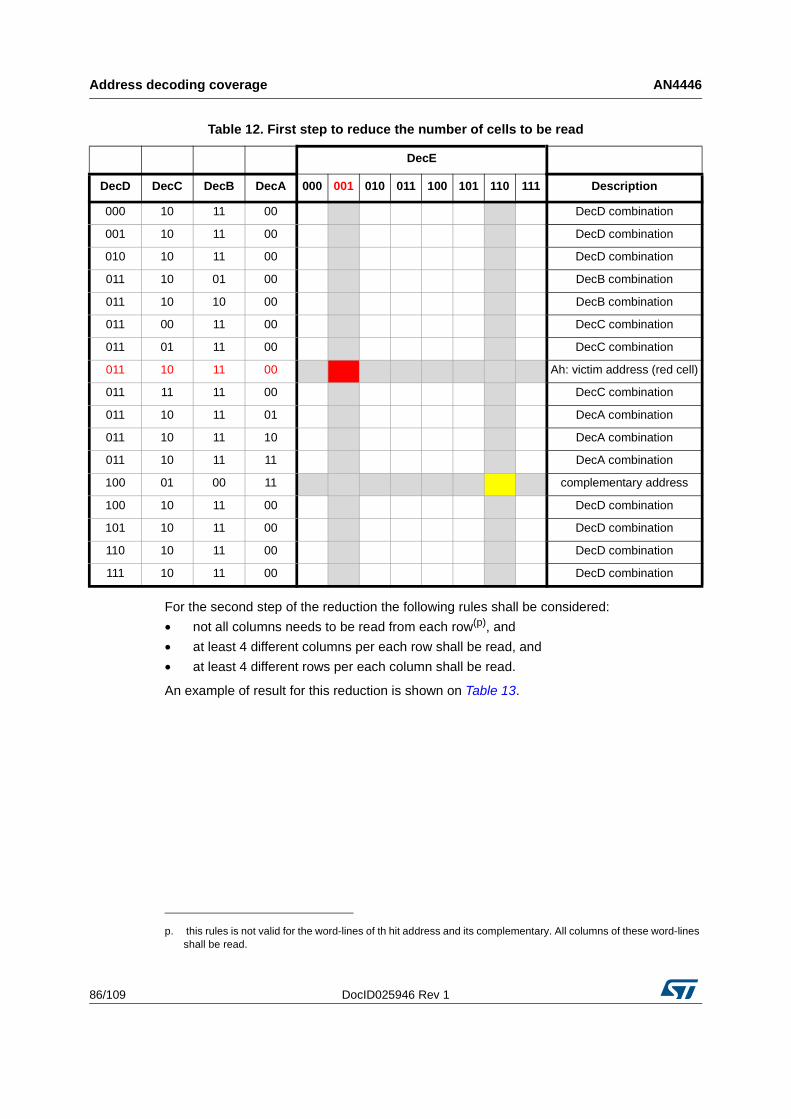
Address decoding coverage AN4446
86/109 DocID025946 Rev 1
For the second step of the reduction the following rules shall be considered:
• not all columns needs to be read from each row(p), and
• at least 4 different columns per each row shall be read, and
• at least 4 different rows per each column shall be read.
An example of result for this reduction is shown on Table 13.
Table 12. First step to reduce the number of cells to be read
DecE
DecD DecC DecB DecA 000 001 010 011 100 101 110 111 Description
000 10 11 00 DecD combination
001 10 11 00 DecD combination
010 10 11 00 DecD combination
011 10 01 00 DecB combination
011 10 10 00 DecB combination
011 00 11 00 DecC combination
011 01 11 00 DecC combination
011 10 11 00 Ah: victim address (red cell)
011 11 11 00 DecC combination
011 10 11 01 DecA combination
011 10 11 10 DecA combination
011 10 11 11 DecA combination
100 01 00 11 complementary address
100 10 11 00 DecD combination
101 10 11 00 DecD combination
110 10 11 00 DecD combination
111 10 11 00 DecD combination
p. this rules is not valid for the word-lines of th hit address and its complementary. All columns of these word-lines shall be read.
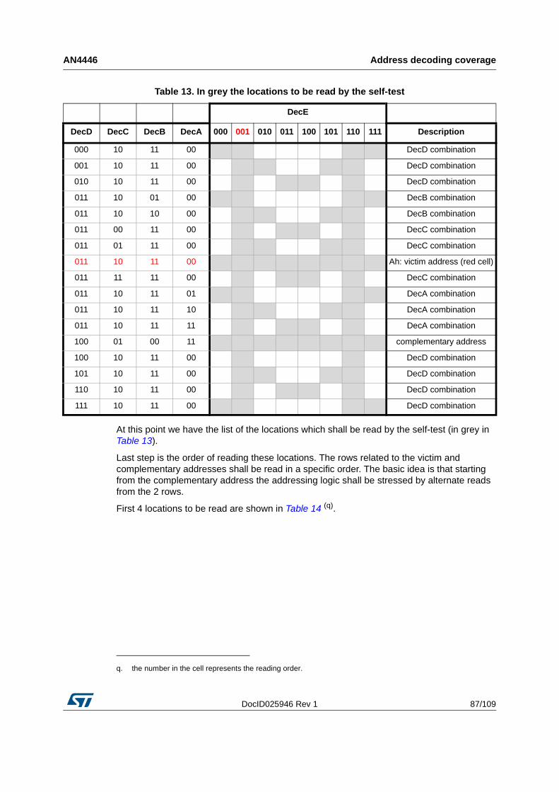
DocID025946 Rev 1 87/109
AN4446 Address decoding coverage
108
At this point we have the list of the locations which shall be read by the self-test (in grey in Table 13).
Last step is the order of reading these locations. The rows related to the victim and complementary addresses shall be read in a specific order. The basic idea is that starting from the complementary address the addressing logic shall be stressed by alternate reads from the 2 rows.
First 4 locations to be read are shown in Table 14 (q).
Table 13. In grey the locations to be read by the self-test
DecE
DecD DecC DecB DecA 000 001 010 011 100 101 110 111 Description
000 10 11 00 DecD combination
001 10 11 00 DecD combination
010 10 11 00 DecD combination
011 10 01 00 DecB combination
011 10 10 00 DecB combination
011 00 11 00 DecC combination
011 01 11 00 DecC combination
011 10 11 00 Ah: victim address (red cell)
011 11 11 00 DecC combination
011 10 11 01 DecA combination
011 10 11 10 DecA combination
011 10 11 11 DecA combination
100 01 00 11 complementary address
100 10 11 00 DecD combination
101 10 11 00 DecD combination
110 10 11 00 DecD combination
111 10 11 00 DecD combination
q. the number in the cell represents the reading order.
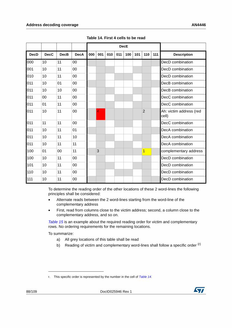
Address decoding coverage AN4446
88/109 DocID025946 Rev 1
To determine the reading order of the other locations of these 2 word-lines the following principles shall be considered:
• Alternate reads between the 2 word-lines starting from the word-line of the complementary address
• First, read from columns close to the victim address; second, a column close to the complementary address, and so on.
Table 15 is an example about the required reading order for victim and complementary rows. No ordering requirements for the remaining locations.
To summarize:
a) All grey locations of this table shall be read
b) Reading of victim and complementary word-lines shall follow a specific order (r)
Table 14. First 4 cells to be read
DecE
DecD DecC DecB DecA 000 001 010 011 100 101 110 111 Description
000 10 11 00 DecD combination
001 10 11 00 DecD combination
010 10 11 00 DecD combination
011 10 01 00 DecB combination
011 10 10 00 DecB combination
011 00 11 00 DecC combination
011 01 11 00 DecC combination
011 10 11 00 4 2 Ah: victim address (red cell)
011 11 11 00 DecC combination
011 10 11 01 DecA combination
011 10 11 10 DecA combination
011 10 11 11 DecA combination
100 01 00 11 3 1 complementary address
100 10 11 00 DecD combination
101 10 11 00 DecD combination
110 10 11 00 DecD combination
111 10 11 00 DecD combination
r. This specific order is represented by the number in the cell of Table 14.
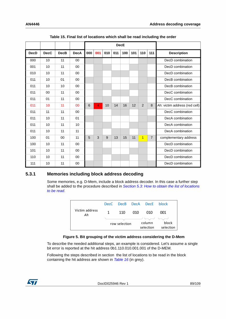
DocID025946 Rev 1 89/109
AN4446 Address decoding coverage
108
5.3.1 Memories including block address decoding
Some memories, e.g. D-Mem, include a block address decoder. In this case a further step shall be added to the procedure described in Section 5.3: How to obtain the list of locations to be read.
Figure 5. Bit grouping of the victim address considering the D-Mem
To describe the needed additional steps, an example is considered. Let’s assume a single bit error is reported at the hit address 0b1.110.010.001.001 of the D-MEM.
Following the steps described in section the list of locations to be read in the block containing the hit address are shown in Table 16 (in grey).
Table 15. Final list of locations which shall be read including the order
DecE
DecD DecC DecB DecA 000 001 010 011 100 101 110 111 Description
000 10 11 00 DecD combination
001 10 11 00 DecD combination
010 10 11 00 DecD combination
011 10 01 00 DecB combination
011 10 10 00 DecB combination
011 00 11 00 DecC combination
011 01 11 00 DecC combination
011 10 11 00 6 4 10 14 16 12 2 8 Ah: victim address (red cell)
011 11 11 00 DecC combination
011 10 11 01 DecA combination
011 10 11 10 DecA combination
011 10 11 11 DecA combination
100 01 00 11 5 3 9 13 15 11 1 7 complementary address
100 10 11 00 DecD combination
101 10 11 00 DecD combination
110 10 11 00 DecD combination
111 10 11 00 DecD combination
DecC DecB DecA DecE block
1 110 010 010 001
row selection blockselection
Victim address Ah
columnselection
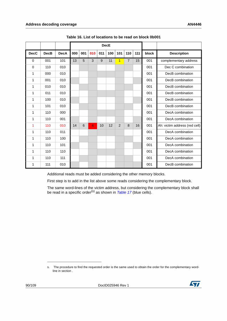
Address decoding coverage AN4446
90/109 DocID025946 Rev 1
Additional reads must be added considering the other memory blocks.
First step is to add in the list above some reads considering the complementary block.
The same word-lines of the victim address, but considering the complementary block shall be read in a specific order(s) as shown in Table 17 (blue cells).
Table 16. List of locations to be read on block 0b001
DecE
DecC DecB DecA 000 001 010 011 100 101 110 111 block Description
0 001 101 13 5 3 9 11 1 7 15 001 complementary address
0 110 010 001 Dec C combination
1 000 010 001 DecB combination
1 001 010 001 DecB combination
1 010 010 001 DecB combination
1 011 010 001 DecB combination
1 100 010 001 DecB combination
1 101 010 001 DecB combination
1 110 000 001 DecA combination
1 110 001 001 DecA combination
1 110 010 14 6 4 10 12 2 8 16 001 Ah: victim address (red cell)
1 110 011 001 DecA combination
1 110 100 001 DecA combination
1 110 101 001 DecA combination
1 110 110 001 DecA combination
1 110 111 001 DecA combination
1 111 010 001 DecB combination
s. The procedure to find the requested order is the same used to obtain the order for the complementary word-line in section .
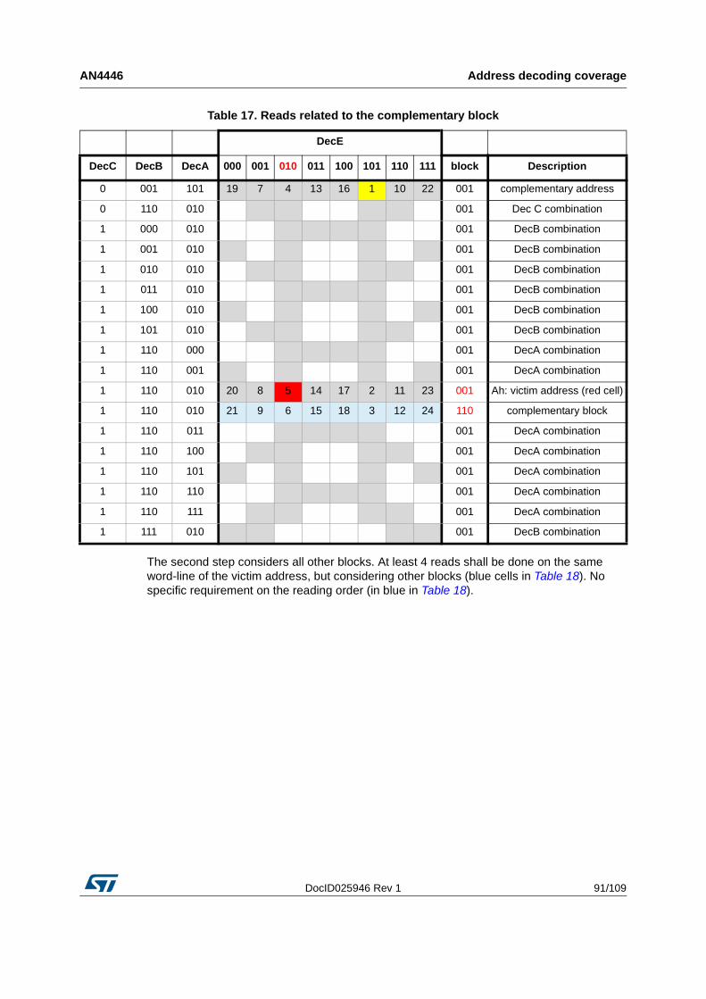
DocID025946 Rev 1 91/109
AN4446 Address decoding coverage
108
The second step considers all other blocks. At least 4 reads shall be done on the same word-line of the victim address, but considering other blocks (blue cells in Table 18). No specific requirement on the reading order (in blue in Table 18).
Table 17. Reads related to the complementary block
DecE
DecC DecB DecA 000 001 010 011 100 101 110 111 block Description
0 001 101 19 7 4 13 16 1 10 22 001 complementary address
0 110 010 001 Dec C combination
1 000 010 001 DecB combination
1 001 010 001 DecB combination
1 010 010 001 DecB combination
1 011 010 001 DecB combination
1 100 010 001 DecB combination
1 101 010 001 DecB combination
1 110 000 001 DecA combination
1 110 001 001 DecA combination
1 110 010 20 8 5 14 17 2 11 23 001 Ah: victim address (red cell)
1 110 010 21 9 6 15 18 3 12 24 110 complementary block
1 110 011 001 DecA combination
1 110 100 001 DecA combination
1 110 101 001 DecA combination
1 110 110 001 DecA combination
1 110 111 001 DecA combination
1 111 010 001 DecB combination
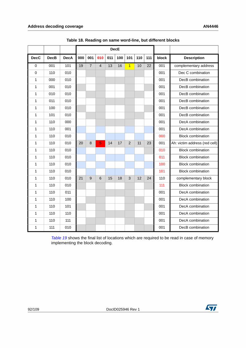
Address decoding coverage AN4446
92/109 DocID025946 Rev 1
Table 19 shows the final list of locations which are required to be read in case of memory implementing the block decoding.
Table 18. Reading on same word-line, but different blocks
DecE
DecC DecB DecA 000 001 010 011 100 101 110 111 block Description
0 001 101 19 7 4 13 16 1 10 22 001 complementary address
0 110 010 001 Dec C combination
1 000 010 001 DecB combination
1 001 010 001 DecB combination
1 010 010 001 DecB combination
1 011 010 001 DecB combination
1 100 010 001 DecB combination
1 101 010 001 DecB combination
1 110 000 001 DecA combination
1 110 001 001 DecA combination
1 110 010 000 Block combination
1 110 010 20 8 5 14 17 2 11 23 001 Ah: victim address (red cell)
1 110 010 010 Block combination
1 110 010 011 Block combination
1 110 010 100 Block combination
1 110 010 101 Block combination
1 110 010 21 9 6 15 18 3 12 24 110 complementary block
1 110 010 111 Block combination
1 110 011 001 DecA combination
1 110 100 001 DecA combination
1 110 101 001 DecA combination
1 110 110 001 DecA combination
1 110 111 001 DecA combination
1 111 010 001 DecB combination
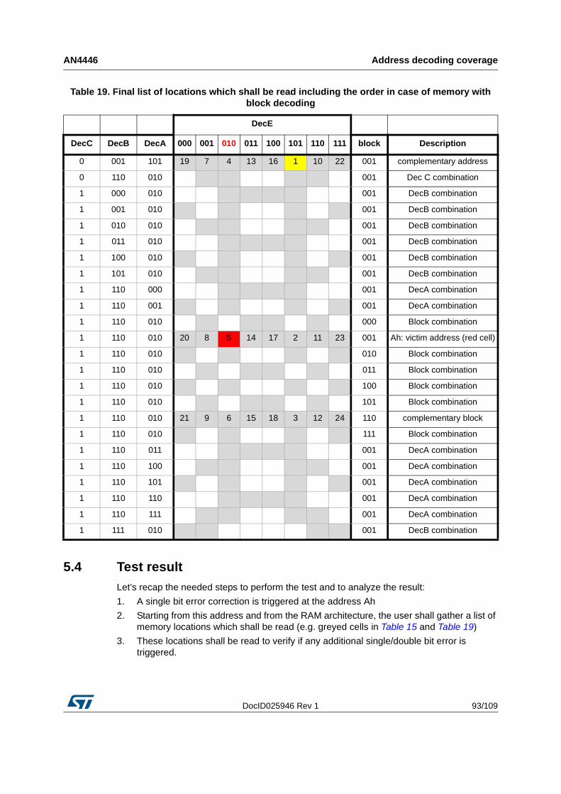
DocID025946 Rev 1 93/109
AN4446 Address decoding coverage
108
5.4 Test resultLet’s recap the needed steps to perform the test and to analyze the result:
1. A single bit error correction is triggered at the address Ah
2. Starting from this address and from the RAM architecture, the user shall gather a list of memory locations which shall be read (e.g. greyed cells in Table 15 and Table 19)
3. These locations shall be read to verify if any additional single/double bit error is triggered.
Table 19. Final list of locations which shall be read including the order in case of memory with block decoding
DecE
DecC DecB DecA 000 001 010 011 100 101 110 111 block Description
0 001 101 19 7 4 13 16 1 10 22 001 complementary address
0 110 010 001 Dec C combination
1 000 010 001 DecB combination
1 001 010 001 DecB combination
1 010 010 001 DecB combination
1 011 010 001 DecB combination
1 100 010 001 DecB combination
1 101 010 001 DecB combination
1 110 000 001 DecA combination
1 110 001 001 DecA combination
1 110 010 000 Block combination
1 110 010 20 8 5 14 17 2 11 23 001 Ah: victim address (red cell)
1 110 010 010 Block combination
1 110 010 011 Block combination
1 110 010 100 Block combination
1 110 010 101 Block combination
1 110 010 21 9 6 15 18 3 12 24 110 complementary block
1 110 010 111 Block combination
1 110 011 001 DecA combination
1 110 100 001 DecA combination
1 110 101 001 DecA combination
1 110 110 001 DecA combination
1 110 111 001 DecA combination
1 111 010 001 DecB combination
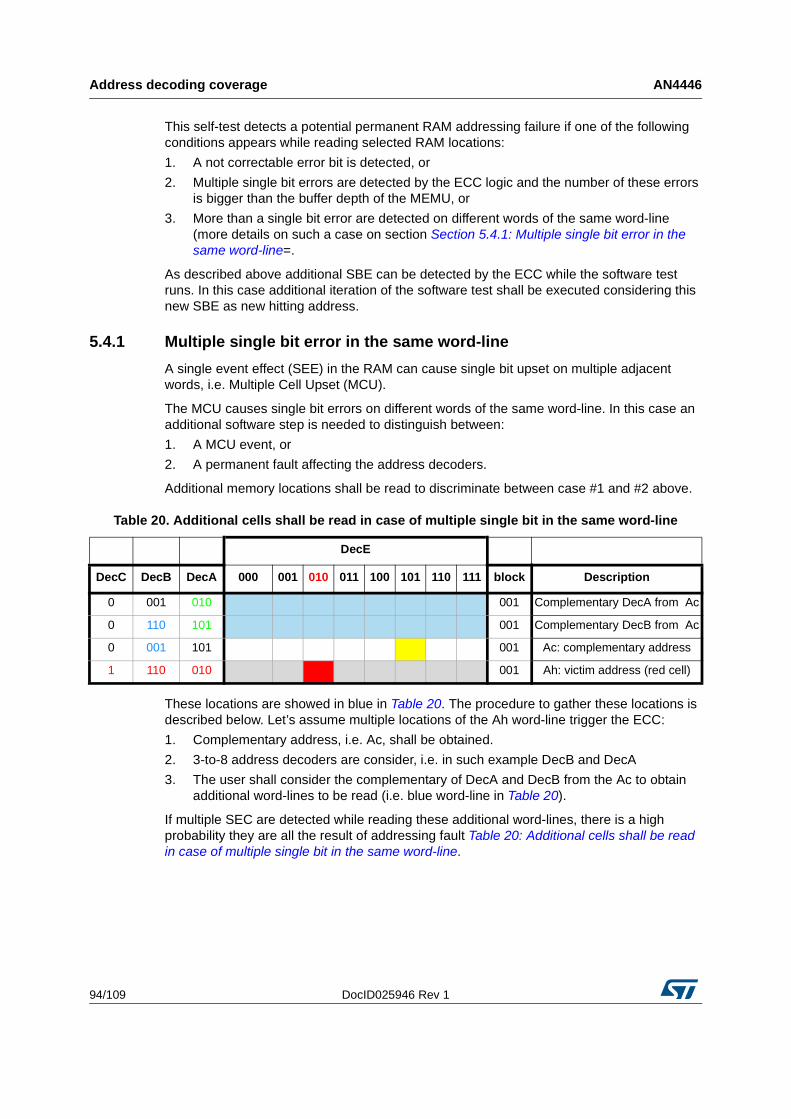
Address decoding coverage AN4446
94/109 DocID025946 Rev 1
This self-test detects a potential permanent RAM addressing failure if one of the following conditions appears while reading selected RAM locations:
1. A not correctable error bit is detected, or
2. Multiple single bit errors are detected by the ECC logic and the number of these errors is bigger than the buffer depth of the MEMU, or
3. More than a single bit error are detected on different words of the same word-line (more details on such a case on section Section 5.4.1: Multiple single bit error in the same word-line=.
As described above additional SBE can be detected by the ECC while the software test runs. In this case additional iteration of the software test shall be executed considering this new SBE as new hitting address.
5.4.1 Multiple single bit error in the same word-line
A single event effect (SEE) in the RAM can cause single bit upset on multiple adjacent words, i.e. Multiple Cell Upset (MCU).
The MCU causes single bit errors on different words of the same word-line. In this case an additional software step is needed to distinguish between:
1. A MCU event, or
2. A permanent fault affecting the address decoders.
Additional memory locations shall be read to discriminate between case #1 and #2 above.
These locations are showed in blue in Table 20. The procedure to gather these locations is described below. Let’s assume multiple locations of the Ah word-line trigger the ECC:
1. Complementary address, i.e. Ac, shall be obtained.
2. 3-to-8 address decoders are consider, i.e. in such example DecB and DecA
3. The user shall consider the complementary of DecA and DecB from the Ac to obtain additional word-lines to be read (i.e. blue word-line in Table 20).
If multiple SEC are detected while reading these additional word-lines, there is a high probability they are all the result of addressing fault Table 20: Additional cells shall be read in case of multiple single bit in the same word-line.
Table 20. Additional cells shall be read in case of multiple single bit in the same word-line
DecE
DecC DecB DecA 000 001 010 011 100 101 110 111 block Description
0 001 010 001 Complementary DecA from Ac
0 110 101 001 Complementary DecB from Ac
0 001 101 001 Ac: complementary address
1 110 010 001 Ah: victim address (red cell)
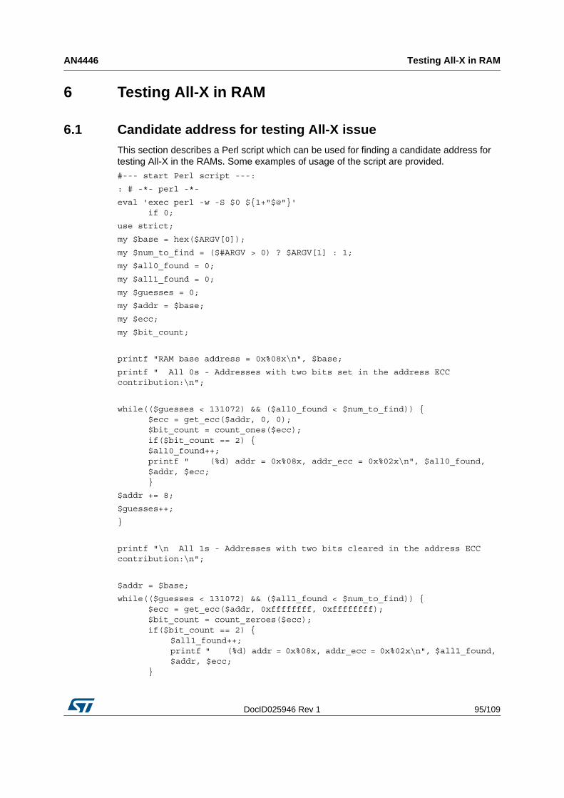
DocID025946 Rev 1 95/109
AN4446 Testing All-X in RAM
108
6 Testing All-X in RAM
6.1 Candidate address for testing All-X issueThis section describes a Perl script which can be used for finding a candidate address for testing All-X in the RAMs. Some examples of usage of the script are provided.
#--- start Perl script ---:
: # -*- perl -*-
eval 'exec perl -w -S $0 ${1+"$@"}'if 0;
use strict;
my $base = hex($ARGV[0]);
my $num_to_find = ($#ARGV > 0) ? $ARGV[1] : 1;
my $all0_found = 0;
my $all1_found = 0;
my $guesses = 0;
my $addr = $base;
my $ecc;
my $bit_count;
printf "RAM base address = 0x%08x\n", $base;
printf " All 0s - Addresses with two bits set in the address ECC contribution:\n";
while(($guesses < 131072) && ($all0_found < $num_to_find)) {$ecc = get_ecc($addr, 0, 0);$bit_count = count_ones($ecc);if($bit_count == 2) {$all0_found++;printf " (%d) addr = 0x%08x, addr_ecc = 0x%02x\n", $all0_found, $addr, $ecc;}
$addr += 8;
$guesses++;
}
printf "\n All 1s - Addresses with two bits cleared in the address ECC contribution:\n";
$addr = $base;
while(($guesses < 131072) && ($all1_found < $num_to_find)) {$ecc = get_ecc($addr, 0xffffffff, 0xffffffff);$bit_count = count_zeroes($ecc);if($bit_count == 2) {
$all1_found++;printf " (%d) addr = 0x%08x, addr_ecc = 0x%02x\n", $all1_found, $addr, $ecc;
}
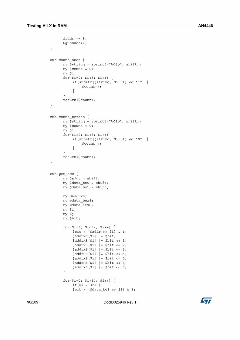
Testing All-X in RAM AN4446
96/109 DocID025946 Rev 1
$addr += 8;$guesses++;
}
sub count_ones {my $string = sprintf("%08b", shift);my $count = 0;my $i;for($i=0; $i<8; $i++) {
if(substr($string, $i, 1) eq "1") {$count++;
}}return($count);
}
sub count_zeroes {my $string = sprintf("%08b", shift);my $count = 0;my $i;for($i=0; $i<8; $i++) {
if(substr($string, $i, 1) eq "0") {$count++;
}}return($count);
}
sub get_ecc {my $addr = shift;my $data_be0 = shift;my $data_be1 = shift;
my @addrx8;my @data_bex8;my @data_lex8;my $i;my $j;my $bit;
for($i=3; $i<32; $i++) {$bit = ($addr >> $i) & 1;$addrx8[$i] = $bit;$addrx8[$i] |= $bit << 1;$addrx8[$i] |= $bit << 2;$addrx8[$i] |= $bit << 3;$addrx8[$i] |= $bit << 4;$addrx8[$i] |= $bit << 5;$addrx8[$i] |= $bit << 6;$addrx8[$i] |= $bit << 7;
}
for($i=0; $i<64; $i++) {if($i < 32) {$bit = ($data_be1 >> $i) & 1;
DocID025946 Rev 1 97/109
AN4446 Testing All-X in RAM
108
} else {$bit = ($data_be0 >> ($i-32)) & 1;
}
$data_bex8[$i] = $bit;$data_bex8[$i] |= $bit << 1;$data_bex8[$i] |= $bit << 2;$data_bex8[$i] |= $bit << 3;$data_bex8[$i] |= $bit << 4;$data_bex8[$i] |= $bit << 5;$data_bex8[$i] |= $bit << 6;$data_bex8[$i] |= $bit << 7;
}
for($i=0; $i<8; $i++) {for($j=0; $j<8; $j++) {
$data_lex8[$i*8+$j] = $data_bex8[(7-$i)*8+$j];}
}
my $addr_ecc= (0x1f & $addrx8[31])^ (0xf4 & $addrx8[30])^ (0x3b & $addrx8[29])^ (0xe3 & $addrx8[28])^ (0x5d & $addrx8[27])^ (0xda & $addrx8[26])^ (0x6e & $addrx8[25])^ (0xb5 & $addrx8[24])^ (0x8f & $addrx8[23])^ (0xd6 & $addrx8[22])^ (0x79 & $addrx8[21])^ (0xba & $addrx8[20])^ (0x9b & $addrx8[19])^ (0xe5 & $addrx8[18])^ (0x57 & $addrx8[17])^ (0xec & $addrx8[16])^ (0xc7 & $addrx8[15])^ (0xae & $addrx8[14])^ (0x67 & $addrx8[13])^ (0x9d & $addrx8[12])^ (0x5b & $addrx8[11])^ (0xe6 & $addrx8[10])^ (0x3e & $addrx8[9])^ (0xf1 & $addrx8[8])^ (0xdc & $addrx8[7])^ (0xe9 & $addrx8[6])^ (0x3d & $addrx8[5])^ (0xf2 & $addrx8[4])^ (0x2f & $addrx8[3]);
my $addr_ecc_tcm= (0x1f & $addrx8[31])^ (0xf4 & $addrx8[30])^ (0x3b & $addrx8[29])
Testing All-X in RAM AN4446
98/109 DocID025946 Rev 1
^ (0xe3 & $addrx8[28])^ (0x5d & $addrx8[27])^ (0xda & $addrx8[26])^ (0x6e & $addrx8[25])^ (0xb5 & $addrx8[24])^ (0x8f & $addrx8[23])^ (0xd6 & $addrx8[22])^ (0x79 & $addrx8[21])^ (0xba & $addrx8[20])^ (0x9b & $addrx8[19])^ (0xe5 & $addrx8[18])^ (0x57 & $addrx8[17])^ (0xec & $addrx8[16]);
my $ecc_tcm_fix= (0xc7 & $addrx8[15])^ (0xae & $addrx8[14])^ (0x67 & $addrx8[13])^ (0x9d & $addrx8[12])^ (0x5b & $addrx8[11])^ (0xe6 & $addrx8[10])^ (0x3e & $addrx8[9])^ (0xf1 & $addrx8[8])^ (0xdc & $addrx8[7])^ (0xe9 & $addrx8[6])^ (0x3d & $addrx8[5])^ (0xf2 & $addrx8[4])^ (0x2f & $addrx8[3]);
my $data_ecc= (0xb0 & $data_lex8[63])^ (0x23 & $data_lex8[62])^ (0x70 & $data_lex8[61])^ (0x62 & $data_lex8[60])^ (0x85 & $data_lex8[59])^ (0x13 & $data_lex8[58])^ (0x45 & $data_lex8[57])^ (0x52 & $data_lex8[56])
^ (0x2a & $data_lex8[55])^ (0x8a & $data_lex8[54])^ (0x0b & $data_lex8[53])^ (0x0e & $data_lex8[52])^ (0xf8 & $data_lex8[51])^ (0x25 & $data_lex8[50])^ (0xd9 & $data_lex8[49])^ (0xa1 & $data_lex8[48])
^ (0x54 & $data_lex8[47])^ (0xa7 & $data_lex8[46])^ (0xa8 & $data_lex8[45])^ (0x92 & $data_lex8[44])^ (0xc8 & $data_lex8[43])^ (0x07 & $data_lex8[42])^ (0x34 & $data_lex8[41])^ (0x32 & $data_lex8[40])
DocID025946 Rev 1 99/109
AN4446 Testing All-X in RAM
108
^ (0x68 & $data_lex8[39])^ (0x89 & $data_lex8[38])^ (0x98 & $data_lex8[37])^ (0x49 & $data_lex8[36])^ (0x61 & $data_lex8[35])^ (0x86 & $data_lex8[34])^ (0x91 & $data_lex8[33])^ (0x46 & $data_lex8[32])
^ (0x58 & $data_lex8[31])^ (0x4f & $data_lex8[30])^ (0x38 & $data_lex8[29])^ (0x75 & $data_lex8[28])^ (0xc4 & $data_lex8[27])^ (0x0d & $data_lex8[26])^ (0xa4 & $data_lex8[25])^ (0x37 & $data_lex8[24])
^ (0x64 & $data_lex8[23])^ (0x16 & $data_lex8[22])^ (0x94 & $data_lex8[21])^ (0x29 & $data_lex8[20])^ (0xea & $data_lex8[19])^ (0x26 & $data_lex8[18])^ (0x1a & $data_lex8[17])^ (0x19 & $data_lex8[16])
^ (0xd0 & $data_lex8[15])^ (0xc2 & $data_lex8[14])^ (0x2c & $data_lex8[13])^ (0x51 & $data_lex8[12])^ (0xe0 & $data_lex8[11])^ (0xa2 & $data_lex8[10])^ (0x1c & $data_lex8[9])^ (0x31 & $data_lex8[8])
^ (0x8c & $data_lex8[7])^ (0x4a & $data_lex8[6])^ (0x4c & $data_lex8[5])^ (0x15 & $data_lex8[4])^ (0x83 & $data_lex8[3])^ (0x9e & $data_lex8[2])^ (0x43 & $data_lex8[1])^ (0xc1 & $data_lex8[0]);
my $ecc = $data_ecc ^ $addr_ecc;my $ecc_tcm = $data_ecc ^ $addr_ecc ^ $addr_ecc_tcm ^ 0x55;my $ecc_flash = $data_ecc ^ 0xff;return($ecc);
}
##printf "addr = 0x%08x\n", $addr;
##printf "data_be = 0x%08x_%08x\n", $data_be0, $data_be1;
##printf "addr_ecc = 0x%02x\n", $addr_ecc;
Testing All-X in RAM AN4446
100/109 DocID025946 Rev 1
##printf "data_ecc = 0x%02x\n", $data_ecc;
##printf "ecc = 0x%02x\n", $ecc;
##printf "ecc_tcm = 0x%02x\n", $ecc_tcm;
##printf "ecc_tcm_fix = 0x%02x\n", $ecc_tcm_fix;
##printf "ecc_flash = 0x%02x\n", $ecc_flash;
#----- end per script -----
This script finds the first N addresses with 2 bits set and 2 bits cleared in the address ECC contribution. Usage is as follows:
• find_allx_addr address [number]
• address – starting address to start searching from
• number – number of addresses to find, default is 1
Example:
1. Find the first address of each type for system RAM:
– ./find_allx_addr 40000000h
RAM base address = 40000000h
All 0s - Addresses with two bits set in the address ECC contribution:
• addr = 40000010h, addr_ecc = 06h
All 1s - Addresses with two bits cleared in the address ECC contribution:
1. addr = 40000008h, addr_ecc = DBh
2. Find the first 5 addresses of each type for system RAM:
– ./find_allx_addr 40000000 5
RAM base address = 40000000h
All 0s - Addresses with two bits set in the address ECC contribution:
1. addr = 40000010h, addr_ecc = 06h
2. addr = 40000038h, addr_ecc = 14h
3. addr = 40000058h, addr_ecc = C0h
4. addr = 40000080h, addr_ecc = 28h
5. addr = 400000F8h, addr_ecc = 21h
All 1s - Addresses with two bits cleared in the address ECC contribution:
1. addr = 40000008h, addr_ecc = DBh
2. addr = 40000098h, addr_ecc = F5h
3. addr = 400000B0h, addr_ecc = E7h
4. addr = 400000C8h, addr_ecc = EEh
5. addr = 400000E0h, addr_ecc = FCh
6.2 ECC checkbit/syndrome coding schemeThe E2E ECC scheme implements a single-error correction, double-error detection (SECDED) code using the so-called Hsiao odd-weight column criteria. These codes are named for M.Y. Hsiao, an IBM researcher who published extensively in the early 1970s on
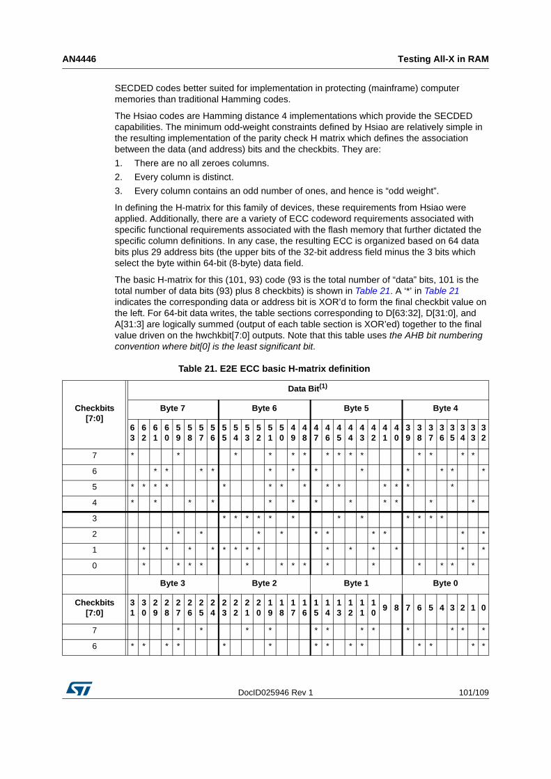
DocID025946 Rev 1 101/109
AN4446 Testing All-X in RAM
108
SECDED codes better suited for implementation in protecting (mainframe) computer memories than traditional Hamming codes.
The Hsiao codes are Hamming distance 4 implementations which provide the SECDED capabilities. The minimum odd-weight constraints defined by Hsiao are relatively simple in the resulting implementation of the parity check H matrix which defines the association between the data (and address) bits and the checkbits. They are:
1. There are no all zeroes columns.
2. Every column is distinct.
3. Every column contains an odd number of ones, and hence is “odd weight”.
In defining the H-matrix for this family of devices, these requirements from Hsiao were applied. Additionally, there are a variety of ECC codeword requirements associated with specific functional requirements associated with the flash memory that further dictated the specific column definitions. In any case, the resulting ECC is organized based on 64 data bits plus 29 address bits (the upper bits of the 32-bit address field minus the 3 bits which select the byte within 64-bit (8-byte) data field.
The basic H-matrix for this (101, 93) code (93 is the total number of “data” bits, 101 is the total number of data bits (93) plus 8 checkbits) is shown in Table 21. A ‘*’ in Table 21 indicates the corresponding data or address bit is XOR’d to form the final checkbit value on the left. For 64-bit data writes, the table sections corresponding to D[63:32], D[31:0], and A[31:3] are logically summed (output of each table section is XOR’ed) together to the final value driven on the hwchkbit[7:0] outputs. Note that this table uses the AHB bit numbering convention where bit[0] is the least significant bit.
Table 21. E2E ECC basic H-matrix definition
Checkbits[7:0]
Data Bit(1)
Byte 7 Byte 6 Byte 5 Byte 4
63
62
61
60
59
58
57
56
55
54
53
52
51
50
49
48
47
46
45
44
43
42
41
40
39
38
37
36
35
34
33
32
7 * * * * * * * * * * * * * *
6 * * * * * * * * * * * *
5 * * * * * * * * * * * * * *
4 * * * * * * * * * * * *
3 * * * * * * * * * * * *
2 * * * * * * * * * *
1 * * * * * * * * * * * * * *
0 * * * * * * * * * * * * * *
Byte 3 Byte 2 Byte 1 Byte 0
Checkbits[7:0]
31
30
29
28
27
26
25
24
23
22
21
20
19
18
17
16
15
14
13
12
11
10
9 8 7 6 5 4 3 2 1 0
7 * * * * * * * * * * * *
6 * * * * * * * * * * * * * *
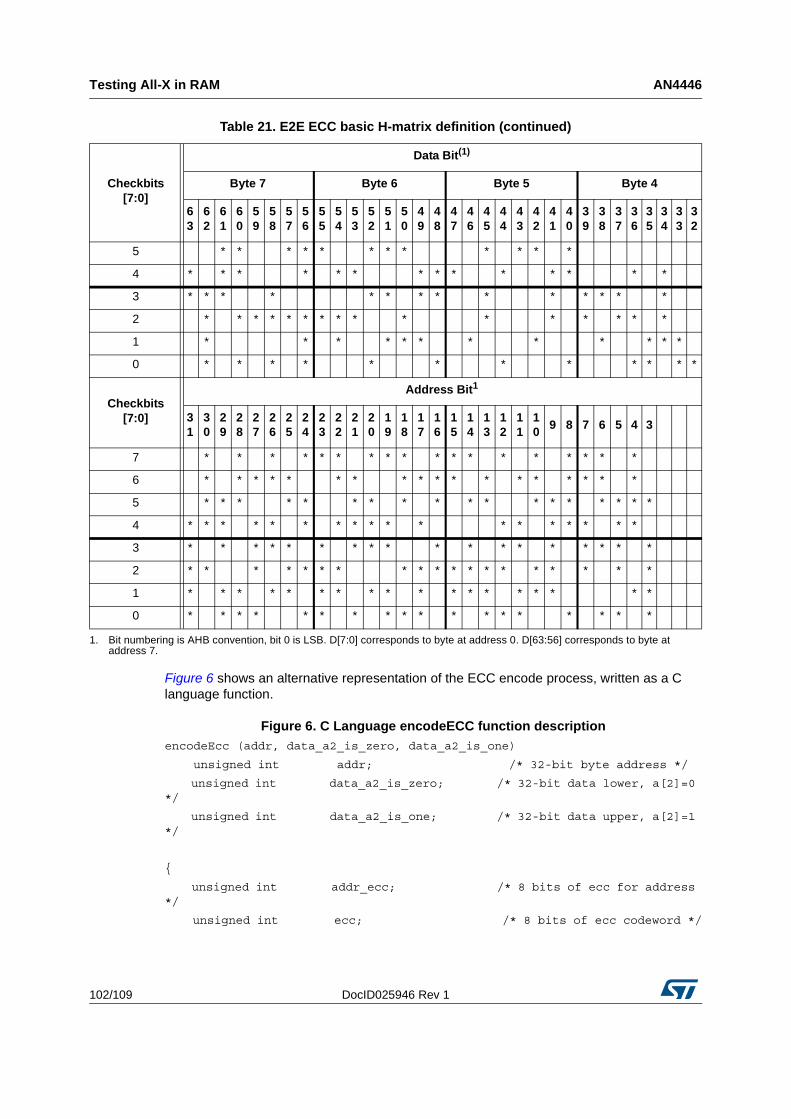
Testing All-X in RAM AN4446
102/109 DocID025946 Rev 1
Figure 6 shows an alternative representation of the ECC encode process, written as a C language function.
Figure 6. C Language encodeECC function descriptionencodeEcc (addr, data_a2_is_zero, data_a2_is_one)
unsigned int addr; /* 32-bit byte address */
unsigned int data_a2_is_zero; /* 32-bit data lower, a[2]=0 */
unsigned int data_a2_is_one; /* 32-bit data upper, a[2]=1 */
{
unsigned int addr_ecc; /* 8 bits of ecc for address */
unsigned int ecc; /* 8 bits of ecc codeword */
5 * * * * * * * * * * * *
4 * * * * * * * * * * * * * *
3 * * * * * * * * * * * * * *
2 * * * * * * * * * * * * * * * *
1 * * * * * * * * * * * *
0 * * * * * * * * * * * *
Checkbits[7:0]
Address Bit1
31
30
29
28
27
26
25
24
23
22
21
20
19
18
17
16
15
14
13
12
11
10
9 8 7 6 5 4 3
7 * * * * * * * * * * * * * * * * * *
6 * * * * * * * * * * * * * * * * * *
5 * * * * * * * * * * * * * * * * * *
4 * * * * * * * * * * * * * * * * * *
3 * * * * * * * * * * * * * * * * * *
2 * * * * * * * * * * * * * * * * * * *
1 * * * * * * * * * * * * * * * * * *
0 * * * * * * * * * * * * * * * * * *
1. Bit numbering is AHB convention, bit 0 is LSB. D[7:0] corresponds to byte at address 0. D[63:56] corresponds to byte at address 7.
Table 21. E2E ECC basic H-matrix definition (continued)
Checkbits[7:0]
Data Bit(1)
Byte 7 Byte 6 Byte 5 Byte 4
63
62
61
60
59
58
57
56
55
54
53
52
51
50
49
48
47
46
45
44
43
42
41
40
39
38
37
36
35
34
33
32
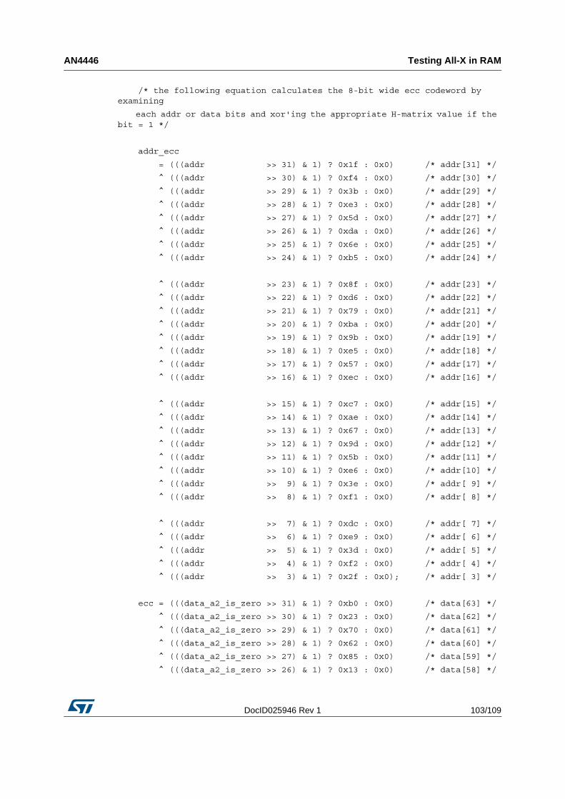
DocID025946 Rev 1 103/109
AN4446 Testing All-X in RAM
108
/* the following equation calculates the 8-bit wide ecc codeword by examining
each addr or data bits and xor'ing the appropriate H-matrix value if the bit = 1 */
addr_ecc
= (((addr >> 31) & 1) ? 0x1f : 0x0) /* addr[31] */
^ (((addr >> 30) & 1) ? 0xf4 : 0x0) /* addr[30] */
^ (((addr >> 29) & 1) ? 0x3b : 0x0) /* addr[29] */
^ (((addr >> 28) & 1) ? 0xe3 : 0x0) /* addr[28] */
^ (((addr >> 27) & 1) ? 0x5d : 0x0) /* addr[27] */
^ (((addr >> 26) & 1) ? 0xda : 0x0) /* addr[26] */
^ (((addr >> 25) & 1) ? 0x6e : 0x0) /* addr[25] */
^ (((addr >> 24) & 1) ? 0xb5 : 0x0) /* addr[24] */
^ (((addr >> 23) & 1) ? 0x8f : 0x0) /* addr[23] */
^ (((addr >> 22) & 1) ? 0xd6 : 0x0) /* addr[22] */
^ (((addr >> 21) & 1) ? 0x79 : 0x0) /* addr[21] */
^ (((addr >> 20) & 1) ? 0xba : 0x0) /* addr[20] */
^ (((addr >> 19) & 1) ? 0x9b : 0x0) /* addr[19] */
^ (((addr >> 18) & 1) ? 0xe5 : 0x0) /* addr[18] */
^ (((addr >> 17) & 1) ? 0x57 : 0x0) /* addr[17] */
^ (((addr >> 16) & 1) ? 0xec : 0x0) /* addr[16] */
^ (((addr >> 15) & 1) ? 0xc7 : 0x0) /* addr[15] */
^ (((addr >> 14) & 1) ? 0xae : 0x0) /* addr[14] */
^ (((addr >> 13) & 1) ? 0x67 : 0x0) /* addr[13] */
^ (((addr >> 12) & 1) ? 0x9d : 0x0) /* addr[12] */
^ (((addr >> 11) & 1) ? 0x5b : 0x0) /* addr[11] */
^ (((addr >> 10) & 1) ? 0xe6 : 0x0) /* addr[10] */
^ (((addr >> 9) & 1) ? 0x3e : 0x0) /* addr[ 9] */
^ (((addr >> 8) & 1) ? 0xf1 : 0x0) /* addr[ 8] */
^ (((addr >> 7) & 1) ? 0xdc : 0x0) /* addr[ 7] */
^ (((addr >> 6) & 1) ? 0xe9 : 0x0) /* addr[ 6] */
^ (((addr >> 5) & 1) ? 0x3d : 0x0) /* addr[ 5] */
^ (((addr >> 4) & 1) ? 0xf2 : 0x0) /* addr[ 4] */
^ (((addr >> 3) & 1) ? 0x2f : 0x0); /* addr[ 3] */
ecc = (((data_a2_is_zero >> 31) & 1) ? 0xb0 : 0x0) /* data[63] */
^ (((data_a2_is_zero >> 30) & 1) ? 0x23 : 0x0) /* data[62] */
^ (((data_a2_is_zero >> 29) & 1) ? 0x70 : 0x0) /* data[61] */
^ (((data_a2_is_zero >> 28) & 1) ? 0x62 : 0x0) /* data[60] */
^ (((data_a2_is_zero >> 27) & 1) ? 0x85 : 0x0) /* data[59] */
^ (((data_a2_is_zero >> 26) & 1) ? 0x13 : 0x0) /* data[58] */
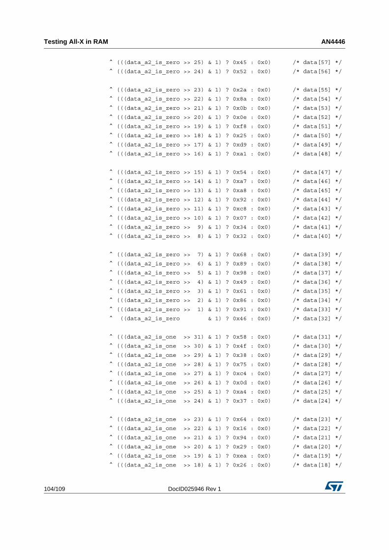
Testing All-X in RAM AN4446
104/109 DocID025946 Rev 1
^ (((data_a2_is_zero >> 25) & 1) ? 0x45 : 0x0) /* data[57] */
^ (((data_a2_is_zero >> 24) & 1) ? 0x52 : 0x0) /* data[56] */
^ (((data_a2_is_zero >> 23) & 1) ? 0x2a : 0x0) /* data[55] */
^ (((data_a2_is_zero >> 22) & 1) ? 0x8a : 0x0) /* data[54] */
^ (((data_a2_is_zero >> 21) & 1) ? 0x0b : 0x0) /* data[53] */
^ (((data_a2_is_zero >> 20) & 1) ? 0x0e : 0x0) /* data[52] */
^ (((data_a2_is_zero >> 19) & 1) ? 0xf8 : 0x0) /* data[51] */
^ (((data_a2_is_zero >> 18) & 1) ? 0x25 : 0x0) /* data[50] */
^ (((data_a2_is_zero >> 17) & 1) ? 0xd9 : 0x0) /* data[49] */
^ (((data_a2_is_zero >> 16) & 1) ? 0xa1 : 0x0) /* data[48] */
^ (((data_a2_is_zero >> 15) & 1) ? 0x54 : 0x0) /* data[47] */
^ (((data_a2_is_zero >> 14) & 1) ? 0xa7 : 0x0) /* data[46] */
^ (((data_a2_is_zero >> 13) & 1) ? 0xa8 : 0x0) /* data[45] */
^ (((data_a2_is_zero >> 12) & 1) ? 0x92 : 0x0) /* data[44] */
^ (((data_a2_is_zero >> 11) & 1) ? 0xc8 : 0x0) /* data[43] */
^ (((data_a2_is_zero >> 10) & 1) ? 0x07 : 0x0) /* data[42] */
^ (((data_a2_is_zero >> 9) & 1) ? 0x34 : 0x0) /* data[41] */
^ (((data_a2_is_zero >> 8) & 1) ? 0x32 : 0x0) /* data[40] */
^ (((data_a2_is_zero >> 7) & 1) ? 0x68 : 0x0) /* data[39] */
^ (((data_a2_is_zero >> 6) & 1) ? 0x89 : 0x0) /* data[38] */
^ (((data_a2_is_zero >> 5) & 1) ? 0x98 : 0x0) /* data[37] */
^ (((data_a2_is_zero >> 4) & 1) ? 0x49 : 0x0) /* data[36] */
^ (((data_a2_is_zero >> 3) & 1) ? 0x61 : 0x0) /* data[35] */
^ (((data_a2_is_zero >> 2) & 1) ? 0x86 : 0x0) /* data[34] */
^ (((data_a2_is_zero >> 1) & 1) ? 0x91 : 0x0) /* data[33] */
^ ((data_a2_is_zero & 1) ? 0x46 : 0x0) /* data[32] */
^ (((data_a2_is_one >> 31) & 1) ? 0x58 : 0x0) /* data[31] */
^ (((data_a2_is_one >> 30) & 1) ? 0x4f : 0x0) /* data[30] */
^ (((data_a2_is_one >> 29) & 1) ? 0x38 : 0x0) /* data[29] */
^ (((data_a2_is_one >> 28) & 1) ? 0x75 : 0x0) /* data[28] */
^ (((data_a2_is_one >> 27) & 1) ? 0xc4 : 0x0) /* data[27] */
^ (((data_a2_is_one >> 26) & 1) ? 0x0d : 0x0) /* data[26] */
^ (((data_a2_is_one >> 25) & 1) ? 0xa4 : 0x0) /* data[25] */
^ (((data_a2_is_one >> 24) & 1) ? 0x37 : 0x0) /* data[24] */
^ (((data_a2_is_one >> 23) & 1) ? 0x64 : 0x0) /* data[23] */
^ (((data_a2_is_one >> 22) & 1) ? 0x16 : 0x0) /* data[22] */
^ (((data_a2_is_one >> 21) & 1) ? 0x94 : 0x0) /* data[21] */
^ (((data_a2_is_one >> 20) & 1) ? 0x29 : 0x0) /* data[20] */
^ (((data_a2_is_one >> 19) & 1) ? 0xea : 0x0) /* data[19] */
^ (((data_a2_is_one >> 18) & 1) ? 0x26 : 0x0) /* data[18] */
DocID025946 Rev 1 105/109
AN4446 Testing All-X in RAM
108
^ (((data_a2_is_one >> 17) & 1) ? 0x1a : 0x0) /* data[17] */
^ (((data_a2_is_one >> 16) & 1) ? 0x19 : 0x0) /* data[16] */
^ (((data_a2_is_one >> 15) & 1) ? 0xd0 : 0x0) /* data[15] */
^ (((data_a2_is_one >> 14) & 1) ? 0xc2 : 0x0) /* data[14] */
^ (((data_a2_is_one >> 13) & 1) ? 0x2c : 0x0) /* data[13] */
^ (((data_a2_is_one >> 12) & 1) ? 0x51 : 0x0) /* data[12] */
^ (((data_a2_is_one >> 11) & 1) ? 0xe0 : 0x0) /* data[11] */
^ (((data_a2_is_one >> 10) & 1) ? 0xa2 : 0x0) /* data[10] */
^ (((data_a2_is_one >> 9) & 1) ? 0x1c : 0x0) /* data[ 9] */
^ (((data_a2_is_one >> 8) & 1) ? 0x31 : 0x0) /* data[ 8] */
^ (((data_a2_is_one >> 7) & 1) ? 0x8c : 0x0) /* data[ 7] */
^ (((data_a2_is_one >> 6) & 1) ? 0x4a : 0x0) /* data[ 6] */
^ (((data_a2_is_one >> 5) & 1) ? 0x4c : 0x0) /* data[ 5] */
^ (((data_a2_is_one >> 4) & 1) ? 0x15 : 0x0) /* data[ 4] */
^ (((data_a2_is_one >> 3) & 1) ? 0x83 : 0x0) /* data[ 3] */
^ (((data_a2_is_one >> 2) & 1) ? 0x9e : 0x0) /* data[ 2] */
^ (((data_a2_is_one >> 1) & 1) ? 0x43 : 0x0) /* data[ 1] */
^ ((data_a2_is_one & 1) ? 0xc1 : 0x0); /* data[ 0] */
ecc = ecc ^ addr_ecc; /* combine data and addr ecc values */
return(ecc);
}
On a memory read operation, the E2E ECC logic performs the same type of optional adjustment on the read checkbits.
As the ECC syndrome is calculated on a read operation by applying the H-matrix to the data plus the checkbits, an all zero syndrome indicates an error free operation. If the generated syndrome value is non-zero and matches one of the H-matrix values associated with the data or checkbits, it represents a single-bit error correction case and the specific bit is complemented to produce the correct data value. If the syndrome value matches one of the H-matrix values associated with the address bits, or is an even weight value, or represents an unused odd weight value, a non-correctable ECC event has been detected and the appropriate error termination response is initiated.
The preceding discussion has provided a generic overview of the end-to-end ECC strategy implemented in this family of automotive MCUs. The next sections discuss specific attributes associated with three different crossbar slave storage groups and their effect on the E2E ECC operation.
Further information AN4446
106/109 DocID025946 Rev 1
Appendix A Further information
A.1 Conventions and terminologyTable 22 shows the list of conventions for this document.
A.2 Acronyms and abbreviationsA short list of acronyms and abbreviations used in this document is shown in Table 23.
Table 22. List of conventions and terminology
Convention Description
error Discrepancy between a computed, observed, or measured value or condition and the true, specified or theoretically correct value or condition.
fault Abnormal condition that may cause a reduction in, or loss of, the capability of a functional unit to perform a required function.
failure The termination of the ability of a functional unit to perform a required function.
Table 23. Acronyms and abbreviations
Terms Meanings
ADC Analog to Digital Converter
BAF Boot Assist Flash
BAR Boot Assist ROM
CCF Common Cause Failure
CMU Clock Monitor Unit
CRC Cyclic Redundancy Check
CTU Cross-Triggering Unit
DC Diagnostic Coverage
ECC Error Correcting Code
DMA Direct Memory Access
ERRM Error Out Monitor function
EXWD External Watchdog function
FCCU Fault Collection and Control Unit
FMEDA Failure Modes, Effects & Diagnostic Analysis
FMPLL Frequency-Modulated Phase-Locked Loop
GPIO General Purpose Input/Output
LBIST Logic Built-In Self-test
MBIST Memory Built-In Self-test
MC_CGM Clock Generation Module
DocID025946 Rev 1 107/109
AN4446 Further information
108
MC_ME Mode Entry
MCU Microcontroller Unit
MPU Memory Protection Unit
NCF Non-Critical Fault
NMI Non-Maskable Interrupt
NVM Non-Volatile Memory
PMU Power Management Unit
PSM Power Supply and Monitor function
PST Process Safety Time
RCCU Redundancy Control Checking Unit
MC_RGM Reset Generation Module
SM Safety Manual
SIL Safety Integrity Level
SSCM System Status and Control Module
SWG Sine Wave Generator
SWT Software Watchdog Timer
Table 23. Acronyms and abbreviations (continued)
Terms Meanings
Document revision history AN4446
108/109 DocID025946 Rev 1
Document revision history
Table 24 summarizes revisions to this document.
Table 24. Document revision history
Date Revision Changes
04-Mar-2014 1 Initial release.
DocID025946 Rev 1 109/109
AN4446
109
Please Read Carefully:
Information in this document is provided solely in connection with ST products. STMicroelectronics NV and its subsidiaries (“ST”) reserve the right to make changes, corrections, modifications or improvements, to this document, and the products and services described herein at any time, without notice.
All ST products are sold pursuant to ST’s terms and conditions of sale.
Purchasers are solely responsible for the choice, selection and use of the ST products and services described herein, and ST assumes no liability whatsoever relating to the choice, selection or use of the ST products and services described herein.
No license, express or implied, by estoppel or otherwise, to any intellectual property rights is granted under this document. If any part of this document refers to any third party products or services it shall not be deemed a license grant by ST for the use of such third party products or services, or any intellectual property contained therein or considered as a warranty covering the use in any manner whatsoever of such third party products or services or any intellectual property contained therein.
UNLESS OTHERWISE SET FORTH IN ST’S TERMS AND CONDITIONS OF SALE ST DISCLAIMS ANY EXPRESS OR IMPLIED WARRANTY WITH RESPECT TO THE USE AND/OR SALE OF ST PRODUCTS INCLUDING WITHOUT LIMITATION IMPLIED WARRANTIES OF MERCHANTABILITY, FITNESS FOR A PARTICULAR PURPOSE (AND THEIR EQUIVALENTS UNDER THE LAWS OF ANY JURISDICTION), OR INFRINGEMENT OF ANY PATENT, COPYRIGHT OR OTHER INTELLECTUAL PROPERTY RIGHT.
ST PRODUCTS ARE NOT DESIGNED OR AUTHORIZED FOR USE IN: (A) SAFETY CRITICAL APPLICATIONS SUCH AS LIFE SUPPORTING, ACTIVE IMPLANTED DEVICES OR SYSTEMS WITH PRODUCT FUNCTIONAL SAFETY REQUIREMENTS; (B) AERONAUTIC APPLICATIONS; (C) AUTOMOTIVE APPLICATIONS OR ENVIRONMENTS, AND/OR (D) AEROSPACE APPLICATIONS OR ENVIRONMENTS. WHERE ST PRODUCTS ARE NOT DESIGNED FOR SUCH USE, THE PURCHASER SHALL USE PRODUCTS AT PURCHASER’S SOLE RISK, EVEN IF ST HAS BEEN INFORMED IN WRITING OF SUCH USAGE, UNLESS A PRODUCT IS EXPRESSLY DESIGNATED BY ST AS BEING INTENDED FOR “AUTOMOTIVE, AUTOMOTIVE SAFETY OR MEDICAL” INDUSTRY DOMAINS ACCORDING TO ST PRODUCT DESIGN SPECIFICATIONS. PRODUCTS FORMALLY ESCC, QML OR JAN QUALIFIED ARE DEEMED SUITABLE FOR USE IN AEROSPACE BY THE CORRESPONDING GOVERNMENTAL AGENCY.
Resale of ST products with provisions different from the statements and/or technical features set forth in this document shall immediately void any warranty granted by ST for the ST product or service described herein and shall not create or extend in any manner whatsoever, any liability of ST.
ST and the ST logo are trademarks or registered trademarks of ST in various countries.Information in this document supersedes and replaces all information previously supplied.
The ST logo is a registered trademark of STMicroelectronics. All other names are the property of their respective owners.
© 2014 STMicroelectronics - All rights reserved
STMicroelectronics group of companies
Australia - Belgium - Brazil - Canada - China - Czech Republic - Finland - France - Germany - Hong Kong - India - Israel - Italy - Japan - Malaysia - Malta - Morocco - Philippines - Singapore - Spain - Sweden - Switzerland - United Kingdom - United States of America
www.st.com


![International Law_100 Ways It Shapes Our Lives [ASIL Booklet]](https://img.pdfslide.us/doc/110x75/55cf8fea550346703ba13833/international-law100-ways-it-shapes-our-lives-asil-booklet.jpg)