Embed Size (px)
Citation preview
May 2015 DocID026771 Rev 2 1/117
1
SPC572L64x, SPC572L60xErrata sheet
SPC572L64F2, SPC572L64E3, SPC572L60F2, SPC572L60E3 device errata JTAG_ID = 0x0AF02041
Introduction
This errata sheet describes all the functional and electrical problems known in the revision 1.0 of the SPC572Lxx devices, identified with the JTAG_ID = 0x0AF02041.
All the topics covered in this document refer to SPC572Lxx reference manual (RM0340 rev 3) and SPC572Lxx datasheet rev 3 (see B.1: Reference document).
Device identification:
Package device marking mask identifier: AA
JTAG_ID = 0x0AF02041
MIDR register:
– MAJOR_MASK: 0
– MINOR_MASK: 0
This errata sheet applies to SPC572Lxx device in accordance with Table 1.
Table 1. Device summary
Part number Package
SPC572L64F2 eTQFP80
SPC572L64E3 eLQFP100
SPC572L60F2 eTQFP80
SPC572L60E3 eLQFP100
www.st.com
Contents SPC572L64x, SPC572L60x
2/117 DocID026771 Rev 2
Contents
1 Functional problems . . . . . . . . . . . . . . . . . . . . . . . . . . . . . . . . . . . . . . . . 13
1.1 ERR003521: DECFIL: Soft reset failures at the end of filtering . . . . . . . . 13
1.2 ERR003877: MC_ME: ME_IMTS[S_DMA] gets set instead of ME_IMTS[S_NMA] on a mode change request to non existing mode . . . 13
1.3 ERR003879: MC_ME: Wakeup from HALT0/STOP0 modes to RUNx may get stalled . . . . . . . . . . . . . . . . . . . . . . . . . . . . . . . . . . . . . . . . . . . . . . . . . 13
1.4 ERR003922: SSCM: Peripheral bus accesses to disabled DSPI, PIT or I2C modules causes device to hang if the SSCM EEROR [RAE] bit is 0 . . . . 14
1.5 ERR003970: NAR: Trace messages include a 6-bit Source Identification field instead of 4- bits . . . . . . . . . . . . . . . . . . . . . . . . . . . . . . . . . . . . . . . . 14
1.6 ERR004048: PAD_RING: Pin drive type (CMOS/OD/LVDS) ignores the ILS setting in MSCR. . . . . . . . . . . . . . . . . . . . . . . . . . . . . . . . . . . . . . . . . . . . 15
1.7 ERR004136: XOSC and IRCOSC: Bus access errors are generated in only half of non- implemented address space of XOSC and IRCOSC, and the other half of address space is mirrored . . . . . . . . . . . . . . . . . . . . . . . . . . 15
1.8 ERR004227: PMC: Temp Sensor User Adjust register size is 5 bits and should be 4 bits. . . . . . . . . . . . . . . . . . . . . . . . . . . . . . . . . . . . . . . . . . . . . 15
1.9 ERR004242: MC_CGM: System Clock Divider Configuration Update cannot be Aligned with Software Trigger . . . . . . . . . . . . . . . . . . . . . . . . . . . . . . . 16
1.10 ERR004248: MC_RGM: Illegal Register Access will not generate access error . . . . . . . . . . . . . . . . . . . . . . . . . . . . . . . . . . . . . . . . . . . . . . . . . . . . . 16
1.11 ERR004249: MC_RGM: 'Destructive' Reset Escalator not Implemented 17
1.12 ERR004250: MC_RGM: ESR0 Deassertion Cannot be Controlled by Software . . . . . . . . . . . . . . . . . . . . . . . . . . . . . . . . . . . . . . . . . . . . . . . . . . 17
1.13 ERR004568: MC_CGM: DE of the CGM_SC_DCn are writable to 0 . . . . 17
1.14 ERR004582: SIPI: Module must be in INIT mode to modify Channel Control Register . . . . . . . . . . . . . . . . . . . . . . . . . . . . . . . . . . . . . . . . . . . . . . . . . . 18
1.15 ERR004583: SIPI: Channel 2 priority is too high . . . . . . . . . . . . . . . . . . . 18
1.16 ERR004764: SSCM: Spurious reset protection missing . . . . . . . . . . . . . 18
1.17 ERR005084: MC_ME: Invalid mode interrupt not generated by MC_ME on illegal write to ME_CADDR0 register . . . . . . . . . . . . . . . . . . . . . . . . . . . . 19
1.18 ERR005085: MC_ME: Access error not generated on writes to read-only ME_CCTL0 register . . . . . . . . . . . . . . . . . . . . . . . . . . . . . . . . . . . . . . . . . 19
1.19 ERR005087: Flash: Short functional reset causes flash error . . . . . . . . . 19
DocID026771 Rev 2 3/117
SPC572L64x, SPC572L60x Contents
11
1.20 ERR005089: MC_ME: Unexpected ICONF_CU interrupt generated on correct mode transition . . . . . . . . . . . . . . . . . . . . . . . . . . . . . . . . . . . . . . . 20
1.21 ERR005116: JDC: Operation of the JTAG Input Data Register Ready bit MSR[JIN_RDY] requires JTAG Clock (TCK) to continue to run after exit from the Update-DR state. . . . . . . . . . . . . . . . . . . . . . . . . . . . . . . . . . . . . . . . . 20
1.22 ERR005118: JDC: MSR[JIN_RDY] and MSR[JIN_INT] will not be cleared if IPS access occurs while JTAG state machine is still in Update-DR state. 20
1.23 ERR005137: JDC: JDC MSR[JOUT_RDY] bit may be cleared even though data from JOUT_IPS has not been read. . . . . . . . . . . . . . . . . . . . . . . . . . 21
1.24 ERR005630: PMC: LVD/HVD EPR registers may not show the source of a destructive reset. . . . . . . . . . . . . . . . . . . . . . . . . . . . . . . . . . . . . . . . . . . . 21
1.25 ERR005639: SSCM: PAE/RAE may not block bus error generation . . . . 22
1.26 ERR005689: GTM: DPLL RAM Region 1 b+c initialization beyond implemented address range . . . . . . . . . . . . . . . . . . . . . . . . . . . . . . . . . . . 22
1.27 ERR005718: SIPI: Channel coding must be the same for the SIPI partner .
. . . . . . . . . . . . . . . . . . . . . . . . . . . . . . . . . . . . . . . . . . . . . . . . . . . . . . . . . 23
1.28 ERR005719: SIUL: MSCR936-967 are not protected through the register protection mechanism . . . . . . . . . . . . . . . . . . . . . . . . . . . . . . . . . . . . . . . 23
1.29 ERR005726: GTM: A CPU write to the BRIDGE_MODE register can result in blocking of the AEI configuration interface . . . . . . . . . . . . . . . . . . . . . . 24
1.30 ERR005749: SDADC: New conversion data is discarded if the overflow (DFORF) status bit is set . . . . . . . . . . . . . . . . . . . . . . . . . . . . . . . . . . . . . 24
1.31 ERR005860: DSPI: Timing does not match specification . . . . . . . . . . . . 25
1.32 ERR005906: GTM: TOM and ATOM inter module triggers delay . . . . . . 25
1.33 ERR005907: GTM: TIM ACB word is incorrect in the case of timeout detection . . . . . . . . . . . . . . . . . . . . . . . . . . . . . . . . . . . . . . . . . . . . . . . . . . 26
1.34 ERR005947: SARADC: ADC may miss a GTM trigger pulse if width of pulse is less than 1 AD Clk cycle . . . . . . . . . . . . . . . . . . . . . . . . . . . . . . . . . . . . 26
1.35 ERR005962: MC_ME: Incorrect setting of ME_IMTS[S_MRIG] bit on illegal mode requests . . . . . . . . . . . . . . . . . . . . . . . . . . . . . . . . . . . . . . . . . . . . . 27
1.36 ERR005978: MC_CGM: System clock dividers generate unaligned divided clocks when programmed back to back and when the first divider is configured for divide by 3 . . . . . . . . . . . . . . . . . . . . . . . . . . . . . . . . . . . . . 27
1.37 ERR005994: FLASH: Prefetch mini-cache enable fields are configurable and default to disabled . . . . . . . . . . . . . . . . . . . . . . . . . . . . . . . . . . . . . . . 28
1.38 ERR006026: DSPI: Incorrect SPI Frame Generated in Combined Serial Interface Configuration . . . . . . . . . . . . . . . . . . . . . . . . . . . . . . . . . . . . . . . 28
1.39 ERR006033: CCCU: software reset may trigger a second interrupt . . . . 29
Contents SPC572L64x, SPC572L60x
4/117 DocID026771 Rev 2
1.40 ERR006041: GTM: TOM and ATOM in center aligned PWM configuration, with CM0=0 or CM0=1 on a triggered channel does not output correct waveform . . . . . . . . . . . . . . . . . . . . . . . . . . . . . . . . . . . . . . . . . . . . . . . . . 29
1.41 ERR006042: SARADC: extra clock cycle when chaining conversion . . . 30
1.42 ERR006072: GTM: Wrong PSTC/PSSC value after initialization and restart of DPLL . . . . . . . . . . . . . . . . . . . . . . . . . . . . . . . . . . . . . . . . . . . . . . . . . . 30
1.43 ERR006073: GTM: MCS channel might not be disabled by the MCU core .
. . . . . . . . . . . . . . . . . . . . . . . . . . . . . . . . . . . . . . . . . . . . . . . . . . . . . . . . . 31
1.44 ERR006077: MC_CGM: Value of CGM_SC_SS[SWTRG] may be incorrect after power-on reset . . . . . . . . . . . . . . . . . . . . . . . . . . . . . . . . . . . . . . . . . 31
1.45 ERR006080: LINFlexD: HRF flag in LINSR (LIN Status Register) is not cleared by hardware . . . . . . . . . . . . . . . . . . . . . . . . . . . . . . . . . . . . . . . . . 32
1.46 ERR006082: LINFlexD: LINS bits in LIN Status Register(LINSR) are not usable in UART mode. . . . . . . . . . . . . . . . . . . . . . . . . . . . . . . . . . . . . . . . 32
1.47 ERR006084: PFLASH: SAFE_CAL feature allows calibration remap when Word 2 of a redundant pair is mismatched. . . . . . . . . . . . . . . . . . . . . . . . 32
1.48 ERR006087: MC_RGM: Reset event during mode transition causes chip to remain in reset . . . . . . . . . . . . . . . . . . . . . . . . . . . . . . . . . . . . . . . . . . . . . 32
1.49 ERR006088: MC_RGM: Requested peripheral reset not applied as expected . . . . . . . . . . . . . . . . . . . . . . . . . . . . . . . . . . . . . . . . . . . . . . . . . . 33
1.50 ERR006090: MC_CGM: CGM_SC_DIV_RC register does not exist . . . . 33
1.51 ERR006091: SDADC/SARADC: coupling current on ADC pin may be present when S/D are not enabled . . . . . . . . . . . . . . . . . . . . . . . . . . . . . . 34
1.52 ERR006099: SDADC: FIFO data corruption is possible in certain configurations of the FIFO threshold . . . . . . . . . . . . . . . . . . . . . . . . . . . . 34
1.53 ERR006349: LINFlexD: Possibility of incorrect break delimiter length in header by LIN master . . . . . . . . . . . . . . . . . . . . . . . . . . . . . . . . . . . . . . . . 35
1.54 ERR006350: LINFlexD: WLS feature cannot be used in buffered mode. 35
1.55 ERR006361: INTC: Interrupt Priority Inversion can occur on a write to INTC_CPRn[PRI] . . . . . . . . . . . . . . . . . . . . . . . . . . . . . . . . . . . . . . . . . . . 35
1.56 ERR006369: PAD_RING: Pull current does not meet updated specification
. . . . . . . . . . . . . . . . . . . . . . . . . . . . . . . . . . . . . . . . . . . . . . . . . . . . . . . . . 36
1.57 ERR006383: SIPI: 16 bit writes/reads may access incorrect addresses . 36
1.58 ERR006409: GTM: ATOM Force Update does not activate a comparison when in SOMC mode . . . . . . . . . . . . . . . . . . . . . . . . . . . . . . . . . . . . . . . . 37
1.59 ERR006410: GTM: Write to ATOM_CH_CTRL sets WRF if CCU0 compare match has already occurred, but CCU1 compare match is pending, in ATOM SOMC mode . . . . . . . . . . . . . . . . . . . . . . . . . . . . . . . . . . . . . . . . . . . . . . . 37
DocID026771 Rev 2 5/117
SPC572L64x, SPC572L60x Contents
11
1.60 ERR006411: GTM: Incorrect Input Signal Characteristics when the TIM channel is in TIEM, TPWM, TIPM, TPIM or TGPS mode, when ECNT is selected as the captured GPRi value. . . . . . . . . . . . . . . . . . . . . . . . . . . . 38
1.61 ERR006412: GTM: Incorrect Input Signal Characteristics when the TIM channel is in TBCM mode and ECNT is selected as the captured GPR0 value. . . . . . . . . . . . . . . . . . . . . . . . . . . . . . . . . . . . . . . . . . . . . . . . . . . . . 38
1.62 ERR006424: LINFlexD: During reception of data, the first packet received could get lost . . . . . . . . . . . . . . . . . . . . . . . . . . . . . . . . . . . . . . . . . . . . . . 39
1.63 ERR006427: LINFlexD: Communication failure when LIN timer is used in Output Compare mode . . . . . . . . . . . . . . . . . . . . . . . . . . . . . . . . . . . . . . . 39
1.64 ERR006428: LINFlexD: Data reception could terminate abruptly in LIN Slave mode when Time-out counter mode is enabled . . . . . . . . . . . . . . . 40
1.65 ERR006477: RGM: minimum PORST pulse is not guaranteed . . . . . . . . 40
1.66 ERR006528: PAD_RING: LVDS cannot be enabled for DSPI_4 by configuring SSS bit field . . . . . . . . . . . . . . . . . . . . . . . . . . . . . . . . . . . . . . 41
1.67 ERR006538: LINFlexD: Stop mode request may be ignored if requested before the end of a frame . . . . . . . . . . . . . . . . . . . . . . . . . . . . . . . . . . . . . 41
1.68 ERR006552: MC_RGM: Reset event during mode transition causes chip to remain in reset . . . . . . . . . . . . . . . . . . . . . . . . . . . . . . . . . . . . . . . . . . . . . 41
1.69 ERR006597: SRX: Pad input low level threshold (Vil) variation is not guaranteed to remain within +/-50mV on 1ms window . . . . . . . . . . . . . . 42
1.70 ERR006638: PASS: Incorrect Censor reset value . . . . . . . . . . . . . . . . . . 42
1.71 ERR006639: GTM: A compare match event does not clear WR_REQ when ATOM is in SOMC mode . . . . . . . . . . . . . . . . . . . . . . . . . . . . . . . . . . . . . 43
1.72 ERR006640: GTM: Valid edge after Timeout event ignored by TIM . . . . 43
1.73 ERR006642: GTM: THVAL not available immediately after inactive trigger in DPLL . . . . . . . . . . . . . . . . . . . . . . . . . . . . . . . . . . . . . . . . . . . . . . . . . . . . 44
1.74 ERR006643: GTM: Incorrect timestamp captured in CNTS when TIM operates in TPWM or TPIM modes if CMU_CLK is not equal to system clock . . . . . . . . . . . . . . . . . . . . . . . . . . . . . . . . . . . . . . . . . . . . . . . . . . . . . . . . . 44
1.75 ERR006644: GTM: Incorrect duty cycle in TOM PCM mode . . . . . . . . . . 44
1.76 ERR006645: GTM: Clearing of DPLL PCM1/2 bits after the Missing Pulse Correction Values calculations delayed . . . . . . . . . . . . . . . . . . . . . . . . . . 45
1.77 ERR006720: SIUL2: Logic state of LVDS input pads cannot be read via GPDI registers. . . . . . . . . . . . . . . . . . . . . . . . . . . . . . . . . . . . . . . . . . . . . . 45
1.78 ERR006792: JDC: The JDC JTAG input IPS data (JIN_IPS) register and JTAG data out (JOUT) register are only reset by JCOMP. . . . . . . . . . . . . 46
1.79 ERR006804: CJTAG: Performing a mode change from Standard Protocol to Advanced Protocol may reset the CJTAG. . . . . . . . . . . . . . . . . . . . . . . . . 46
Contents SPC572L64x, SPC572L60x
6/117 DocID026771 Rev 2
1.80 ERR006815: PASS: Debug access in "OEM Production" Life Cycle UNLOCKED if no DCF record is programmed. . . . . . . . . . . . . . . . . . . . . 47
1.81 ERR006816: PASS: Debug port may be enabled during functional reset 47
1.82 ERR006819: Flash: Flash read protection may be active in life cycle stage 'OEM production' . . . . . . . . . . . . . . . . . . . . . . . . . . . . . . . . . . . . . . . . . . . 47
1.83 ERR006836: DCF: DCF record for initial IVPR cannot be used . . . . . . . 48
1.84 ERR006839: RGM: Out of temperature range Destructive Reset enable / disable feature is available in RGM_DERD[D_TSR_DEST]. . . . . . . . . . . 48
1.85 ERR006847: INTC: PLL interrupts are implemented in IRQs 480, 482, 484-487 . . . . . . . . . . . . . . . . . . . . . . . . . . . . . . . . . . . . . . . . . . . . . . . . . . . . . . 49
1.86 ERR006860: PRAMC: PRCR1[P0_BO_DIS] and PRCR1[P1_B0_DIS] always read as zero . . . . . . . . . . . . . . . . . . . . . . . . . . . . . . . . . . . . . . . . . 49
1.87 ERR006902: RGM: short functional reset may cause multiple ESR0 pulses when Progressive Clock Switching is configured . . . . . . . . . . . . . . . . . . . 50
1.88 ERR006904: DSPI: Reads the RXFRx causes failures of subsequent DSPI register reads . . . . . . . . . . . . . . . . . . . . . . . . . . . . . . . . . . . . . . . . . . . . . . 50
1.89 ERR006905: DSPI: When Extended SPI Mode is used to transmit frames of size > 16 bits, outgoing frames can be corrupted. . . . . . . . . . . . . . . . . . . 51
1.90 ERR006906: SDADC: Invalid conversion data when output settling delay value is less than 23 . . . . . . . . . . . . . . . . . . . . . . . . . . . . . . . . . . . . . . . . . 51
1.91 ERR006915: LINFlexD: Erroneous receiver interrupt generation in UART FIFO mode . . . . . . . . . . . . . . . . . . . . . . . . . . . . . . . . . . . . . . . . . . . . . . . . 52
1.92 ERR006916: M_CAN: Rx FIFO overwrite mode, transmit pause and CAN FD 64-byte frames not supported . . . . . . . . . . . . . . . . . . . . . . . . . . . . . . . 52
1.93 ERR006928: PASS: PASS module debug is not controllable during reset of after reset . . . . . . . . . . . . . . . . . . . . . . . . . . . . . . . . . . . . . . . . . . . . . . . . . 53
1.94 ERR006967: eDMA: Possible misbehavior of a preempted channel when using continuous link mode . . . . . . . . . . . . . . . . . . . . . . . . . . . . . . . . . . . 54
1.95 ERR006990: CJTAG: possible incorrect TAP state machine advance during Check Packet . . . . . . . . . . . . . . . . . . . . . . . . . . . . . . . . . . . . . . . . . . . . . . 54
1.96 ERR007013: LINFlexD: Auto synchronization functionality does not work as intended . . . . . . . . . . . . . . . . . . . . . . . . . . . . . . . . . . . . . . . . . . . . . . . . . . 55
1.97 ERR007053: M_CAN: Accesses to disabled M_(TT)_CAN modules causes device to hang . . . . . . . . . . . . . . . . . . . . . . . . . . . . . . . . . . . . . . . . . . . . . 55
1.98 ERR007057: SIUL2: Incorrect MSCR reset value for pins PA[9:4], PB[11] and PC[2] . . . . . . . . . . . . . . . . . . . . . . . . . . . . . . . . . . . . . . . . . . . . . . . . . 56
1.99 ERR007061: SPU: Reserved location can be written . . . . . . . . . . . . . . . 56
1.100 ERR007067: IRCOSC: Reduced accuracy of the software trimming . . . . 56
DocID026771 Rev 2 7/117
SPC572L64x, SPC572L60x Contents
11
1.101 ERR007083: GTM: The DPLL's SORI, TORI, MTI, and MSI interrupts may not be asserted . . . . . . . . . . . . . . . . . . . . . . . . . . . . . . . . . . . . . . . . . . . . 57
1.102 ERR007084: GTM: An active edge input, that is rejected by the DPLL trigger plausibility check, does not assert a Missing Trigger Interrupt . . . . . . . . . 57
1.103 ERR007085: GTM: A TIM timeout occurs when the TDU is re-enabled . 58
1.104 ERR007086: GTM: TIM PWM and PIM modes may capture the wrong timestamp . . . . . . . . . . . . . . . . . . . . . . . . . . . . . . . . . . . . . . . . . . . . . . . . . 58
1.105 ERR007087: GTM: The DPLL's Address Pointer Extension value is added to the Address Pointer when the Address Pointer Status bit is 0 . . . . . . . 59
1.106 ERR007088: GTM: When ATOM is in SOMP mode the SR0/SR1 registers could be updated twice in one PWM period . . . . . . . . . . . . . . . . . . . . . . . 59
1.107 ERR007103: MC_CGM: Incorrect cause for the latest clock source switch may be reported by the CGM if a safe mode request arrives when the system clock is the IRC . . . . . . . . . . . . . . . . . . . . . . . . . . . . . . . . . . . . . . 60
1.108 ERR007108: SARADC: Spikes on external multiplexer signals . . . . . . . . 60
1.109 ERR007111: DMA: DMA does not work properly with M_CAN modules . 61
1.110 ERR007113: DMA: GTM accesses via DMA may fail . . . . . . . . . . . . . . . 61
1.111 ERR007115: DSPI: Mixing 16 and 32 bits frame size in XSPI Mode can cause incorrect data to be transmitted . . . . . . . . . . . . . . . . . . . . . . . . . . . 61
1.112 ERR007124: FLASH: unexpected behavior when resuming from an Array Integrity check or a Margin read suspend if both NAIBP and AISUS bits are set . . . . . . . . . . . . . . . . . . . . . . . . . . . . . . . . . . . . . . . . . . . . . . . . . . . . . . 62
1.113 ERR007125: FLASH: wrong signature if an Array Integrity check or Margin read is suspended too early . . . . . . . . . . . . . . . . . . . . . . . . . . . . . . . . . . . 63
1.114 ERR007130: FLASH: Incorrect termination of program sequence when the Program bit is cleared before the Enable High Voltage bit is set . . . . . . . 63
1.115 ERR007131: FLASH: Incorrect termination of erase sequence when Erase bit is cleared before Enable High Voltage bit is set . . . . . . . . . . . . . . . . . 64
1.116 ERR007138: SARADC: Missed conversion after ABORT of the last channel of an injected chain . . . . . . . . . . . . . . . . . . . . . . . . . . . . . . . . . . . . . . . . . 64
1.117 ERR007185: SDADC: Watchdog Crossover event missed if PBRIDGEx_CLK less than SD_CLK . . . . . . . . . . . . . . . . . . . . . . . . . . . . 65
1.118 ERR007190: GTM: Simultaneous Core and DPLL accesses to RAM Region 2 may lead to the DPLL reading erroneous data . . . . . . . . . . . . . . . . . . . 65
1.119 ERR007191: GTM: The DPLL's SORI and TORI interrupts are not asserted
. . . . . . . . . . . . . . . . . . . . . . . . . . . . . . . . . . . . . . . . . . . . . . . . . . . . . . . . . 66
1.120 ERR007194: MC_ME: IMTS bit 26 is S_MRIG . . . . . . . . . . . . . . . . . . . . 67
Contents SPC572L64x, SPC572L60x
8/117 DocID026771 Rev 2
1.121 ERR007202: SENT: Increased tolerance to noise for Nibble length measurement is not available . . . . . . . . . . . . . . . . . . . . . . . . . . . . . . . . . . 67
1.122 ERR007203: SENT: In debug mode SENT message data registers appear to lose contents . . . . . . . . . . . . . . . . . . . . . . . . . . . . . . . . . . . . . . . . . . . . 68
1.123 ERR007204: SENT: Number of Expected Edges Error status flag spuriously set when operating with Option 1 of the Successive Calibration Check method . . . . . . . . . . . . . . . . . . . . . . . . . . . . . . . . . . . . . . . . . . . . . . . . . . . 68
1.124 ERR007222: SARADC: Minimum value of precharge must be greater than or equal to 2 ADC clock cycles . . . . . . . . . . . . . . . . . . . . . . . . . . . . . . . . . 69
1.125 ERR007246: SARADC: First conversion after exit from stop mode may be corrupted . . . . . . . . . . . . . . . . . . . . . . . . . . . . . . . . . . . . . . . . . . . . . . . . . 69
1.126 ERR007259: e200zx: ICNT and branch history information may be incorrect following a nexus overflow . . . . . . . . . . . . . . . . . . . . . . . . . . . . . . . . . . . . 70
1.127 ERR007274: LINFlexD: Consecutive headers received by LIN Slave triggers the LIN FSM to an unexpected state . . . . . . . . . . . . . . . . . . . . . . . . . . . . 71
1.128 ERR007297: LINFlexD: Response timeout values is loaded in LINOCR[OC2] field instead of LINOCR[OC1] . . . . . . . . . . . . . . . . . . . . . 71
1.129 ERR007305: e200zx: JTAG reads of the Performance Monitor Counter registers are not reliable . . . . . . . . . . . . . . . . . . . . . . . . . . . . . . . . . . . . . . 72
1.130 ERR007348: SIUL2: PD[2] pin, medium and strong driver strength not available . . . . . . . . . . . . . . . . . . . . . . . . . . . . . . . . . . . . . . . . . . . . . . . . . . 72
1.131 ERR007349: OVLY RAM: Overlay SRAM may not be accessible after power on . . . . . . . . . . . . . . . . . . . . . . . . . . . . . . . . . . . . . . . . . . . . . . . . . . . . . . . 72
1.132 ERR007356: SDADC: The SDADC FIFO does not function correctly when FIFO overwrite option is used . . . . . . . . . . . . . . . . . . . . . . . . . . . . . . . . . 73
1.133 ERR007360: FEC: Minimum VDD is 3.15 V instead of 3.0 V . . . . . . . . . 73
1.134 ERR007362: SDADC: Additional DMA request generated after single read access . . . . . . . . . . . . . . . . . . . . . . . . . . . . . . . . . . . . . . . . . . . . . . . . . . . 74
1.135 ERR007404: SENT: Message overflow in SENT Receiver can lead to stall condition in the MCU . . . . . . . . . . . . . . . . . . . . . . . . . . . . . . . . . . . . . . . . 74
1.136 ERR007414: PBRIDGE: Incorrect transfer error when accessing reserved locations of the Peripheral Bridge . . . . . . . . . . . . . . . . . . . . . . . . . . . . . . 75
1.137 ERR007415: JTAG: PA[9] = JTAG TDO pad is not pull-up during reset . 76
1.138 ERR007417: SDADC: Gain error above specification after calibration . . 76
1.139 ERR007425: SENT: Unexpected NUM_EDGES_ERR error in certain conditions when message has a pause pulse . . . . . . . . . . . . . . . . . . . . . 76
1.140 ERR007433: JTAGM: Nexus error bit is cleared by successful RWA . . . 78
1.141 ERR007438: PMC: Temperature digital outputs not available . . . . . . . . . 79
DocID026771 Rev 2 9/117
SPC572L64x, SPC572L60x Contents
11
1.142 ERR007454: PMC: LVD10_C, LVD10_F, LVD10_IJ generate POR when set
. . . . . . . . . . . . . . . . . . . . . . . . . . . . . . . . . . . . . . . . . . . . . . . . . . . . . . . . . 79
1.143 ERR007488: PMC: The Reset Enable bits default values cannot be set in the DCF records . . . . . . . . . . . . . . . . . . . . . . . . . . . . . . . . . . . . . . . . . . . . 80
1.144 ERR007489: SDADC: Common Voltage Bias Selection bit behavior . . . 80
1.145 ERR007502: PBRIDGE: Incorrect transfer error information for accesses to FEC reserved locations . . . . . . . . . . . . . . . . . . . . . . . . . . . . . . . . . . . . . . 80
1.146 ERR007503: PMC: LVD400 on ADC supply (VDD_HV_ADV) must not be disabled . . . . . . . . . . . . . . . . . . . . . . . . . . . . . . . . . . . . . . . . . . . . . . . . . . 81
1.147 ERR007528: GTM: Action not always calculated immediately by DPLL . 81
1.148 ERR007529: GTM: TIM overflow bit is not set and the signal level bit has inverse value when sent to ARU in some cases . . . . . . . . . . . . . . . . . . . 82
1.149 ERR007530: GTM: New DPLL Position Minus Time data not received . . 83
1.150 ERR007531: GTM: DPLL Position Minus Time result is not sent to the ARU
. . . . . . . . . . . . . . . . . . . . . . . . . . . . . . . . . . . . . . . . . . . . . . . . . . . . . . . . . 83
1.151 ERR007538: M_(TT)CAN: Switch between CAN operating modes during transmission or reception may be ignored . . . . . . . . . . . . . . . . . . . . . . . . 84
1.152 ERR007587: SSCM: Multi-bit ECC error at RCHW locations will cause device to remain in reset as a security and safety precaution . . . . . . . . . 85
1.153 ERR007589: LINFlexD: Spurious timeout error when switching from UART to LIN mode or when resetting LINTCSR[MODE] bit in LIN mode . . . . . . 86
1.154 ERR007788: SIUL2: A transfer error is not generated for 8-bit accesses to non-existent MSCRs . . . . . . . . . . . . . . . . . . . . . . . . . . . . . . . . . . . . . . . . 86
1.155 ERR007791: SIUL2: Transfer error not generated if reserved addresses within the range of SIUL BASE + 0x100 to 0x23F are accessed . . . . . . . 87
1.156 ERR007824: DCI: Avoid asserting system reset when switching JTAG operating modes . . . . . . . . . . . . . . . . . . . . . . . . . . . . . . . . . . . . . . . . . . . . 87
1.157 ERR007846: GTM: Assertion of DPLL's LOCK1 flag may be delayed by one event . . . . . . . . . . . . . . . . . . . . . . . . . . . . . . . . . . . . . . . . . . . . . . . . . . . . 87
1.158 ERR007847: GTM: MCS's CAT status may be incorrect . . . . . . . . . . . . . 88
1.159 ERR007848: GTM: Bit 0 of TIM edge counter register may not indicate the actual signal level . . . . . . . . . . . . . . . . . . . . . . . . . . . . . . . . . . . . . . . . . . . 88
1.160 ERR007855: SENT: Integer division during calibration pulse measurement causes reduced robustness . . . . . . . . . . . . . . . . . . . . . . . . . . . . . . . . . . . 88
1.161 ERR007886: SENT: Jitter tolerance is limited to 1/8 of the utick time . . . 89
1.162 ERR007906: SARADC: The Data Overwritten flag bits in the SARADC may not be valid . . . . . . . . . . . . . . . . . . . . . . . . . . . . . . . . . . . . . . . . . . . . . . . . 89
1.163 ERR007934: FEC: MDC and MDIO timing requirements and configuration
Contents SPC572L64x, SPC572L60x
10/117 DocID026771 Rev 2
. . . . . . . . . . . . . . . . . . . . . . . . . . . . . . . . . . . . . . . . . . . . . . . . . . . . . . . . . 90
1.164 ERR007947: XOSC: Incorrect external oscillator status flag after CMU event clear . . . . . . . . . . . . . . . . . . . . . . . . . . . . . . . . . . . . . . . . . . . . . . . . . . . . . 90
1.165 ERR008039: SDADC: digital filter and FIFO not disabled when MCR[EN] is cleared . . . . . . . . . . . . . . . . . . . . . . . . . . . . . . . . . . . . . . . . . . . . . . . . . . . 90
1.166 ERR008054: PIT: DMA request stays asserted when initiated by PIT trigger, until PIT is reset . . . . . . . . . . . . . . . . . . . . . . . . . . . . . . . . . . . . . . . . . . . . 91
1.167 ERR008082: SENT: A message overflow can lead to a loss of frames combined with NUM_EDGES_ERR being set . . . . . . . . . . . . . . . . . . . . . 91
1.168 ERR008122: GTM: (A)TOM's CCU1 event interrupt is not generated when CM1=0 or 1 and RST_CCU0=1 . . . . . . . . . . . . . . . . . . . . . . . . . . . . . . . . 92
1.169 ERR008123: SPC572L64: Current injection causes leakage path across the DSPI and LFAST LVDS pins . . . . . . . . . . . . . . . . . . . . . . . . . . . . . . . . . . 93
1.170 ERR008130: PAD_RING: No TTL levels on JTAG pins . . . . . . . . . . . . . . 93
1.171 ERR008429: GTM: Unexpected TIM CNTS register reset in TPWM OSM mode . . . . . . . . . . . . . . . . . . . . . . . . . . . . . . . . . . . . . . . . . . . . . . . . . . . . 94
1.172 ERR008438: GTM: Wrong signal level when TIM mode is changed from TBCM to any other mode . . . . . . . . . . . . . . . . . . . . . . . . . . . . . . . . . . . . . 94
1.173 ERR008439: GTM: TOM and ATOM CM0, CM1 and CLK_SRC register updates may not be triggered . . . . . . . . . . . . . . . . . . . . . . . . . . . . . . . . . . 95
1.174 ERR008526: LINFlexD: LIN or UART state may be incorrectly indicated by LINSR[LINS] bitfield . . . . . . . . . . . . . . . . . . . . . . . . . . . . . . . . . . . . . . . . . 96
1.175 ERR008561: LINFlexD: Corruption of Tx data in LIN mode with DMA feature enabled . . . . . . . . . . . . . . . . . . . . . . . . . . . . . . . . . . . . . . . . . . . . . . . . . . 96
1.176 ERR008602: LINFlexD: Tx through DMA can be re-triggered after abort in LIN/UART modes or can prematurely end on the event of bit error with LINCR2[IOBE] bit being set in LIN mode . . . . . . . . . . . . . . . . . . . . . . . . . 97
1.177 ERR008631: SDADC: low threshold watchdog cannot be used with signed data . . . . . . . . . . . . . . . . . . . . . . . . . . . . . . . . . . . . . . . . . . . . . . . . . . . . . 97
1.178 ERR008688: GTM: Data lost in ATOM when CMU_CLKx is slower than ARU . . . . . . . . . . . . . . . . . . . . . . . . . . . . . . . . . . . . . . . . . . . . . . . . . . . . . 98
1.179 ERR008689: GTM: F2A stream data are not deleted after stream disabling
. . . . . . . . . . . . . . . . . . . . . . . . . . . . . . . . . . . . . . . . . . . . . . . . . . . . . . . . . 98
1.180 ERR008915: SARADC: wrong behavior when aborting the conversion of a chain . . . . . . . . . . . . . . . . . . . . . . . . . . . . . . . . . . . . . . . . . . . . . . . . . . . . . 99
1.181 ERR008919: SPC572L64: LC set to ST_Production . . . . . . . . . . . . . . . . 99
1.182 ERR008933: LINFlexD: Inconsistent sync field may cause an incorrect baud rate and Sync Field Error Flag may not be set . . . . . . . . . . . . . . . 100
DocID026771 Rev 2 11/117
SPC572L64x, SPC572L60x Contents
11
1.183 ERR008935: JTAGM: write accesses to registers must be 32-bit wide . 101
1.184 ERR008970: LINFlexD: Spurious bit error in extended frame mode may cause an incorrect Idle State . . . . . . . . . . . . . . . . . . . . . . . . . . . . . . . . . 101
1.185 ERR009048: PAD_RING: No Automotive input levels for PA[0] and PA[13]
. . . . . . . . . . . . . . . . . . . . . . . . . . . . . . . . . . . . . . . . . . . . . . . . . . . . . . . . 101
1.186 ERR009049: PAD_RING: Hysteresis cannot be disabled in CMOS mode configuration for PC[12] . . . . . . . . . . . . . . . . . . . . . . . . . . . . . . . . . . . . . 102
1.187 ERR009082: LINFlexD: Corruption of Received Rx data in UART mode 102
1.188 ERR009083: PBRIDGE: Incorrect transfer error information for accesses to PLLDIG reserved locations . . . . . . . . . . . . . . . . . . . . . . . . . . . . . . . . . . 103
1.189 ERR009086: PASS: JTAG password overrides Flash memory read protection . . . . . . . . . . . . . . . . . . . . . . . . . . . . . . . . . . . . . . . . . . . . . . . . 103
1.190 ERR009089: PBRIDGE: Incorrect transfer error information for accesses to MC_CGM and MC_RGM reserved locations . . . . . . . . . . . . . . . . . . . . . 104
1.191 ERR009215: PAD_RING: Higher output impedance on PC[12] when Ethernet I/O segment is configured for 3.3V supply . . . . . . . . . . . . . . . . 104
1.192 ERR009343: PAD_RING: Differential DSPI with SIN LVDS signal pairs is not supported . . . . . . . . . . . . . . . . . . . . . . . . . . . . . . . . . . . . . . . . . . . . . . . . 105
Appendix A Defect across silicon version . . . . . . . . . . . . . . . . . . . . . . . . . . . . . 106
Appendix B Further information . . . . . . . . . . . . . . . . . . . . . . . . . . . . . . . . . . . . . 114
B.1 Reference document . . . . . . . . . . . . . . . . . . . . . . . . . . . . . . . . . . . . . . . . .114
B.2 Acronyms . . . . . . . . . . . . . . . . . . . . . . . . . . . . . . . . . . . . . . . . . . . . . . . . .114
Revision history . . . . . . . . . . . . . . . . . . . . . . . . . . . . . . . . . . . . . . . . . . . . . . . . . . . 116
List of tables SPC572L64x, SPC572L60x
12/117 DocID026771 Rev 2
List of tables
Table 1. Device summary . . . . . . . . . . . . . . . . . . . . . . . . . . . . . . . . . . . . . . . . . . . . . . . . . . . . . . . . . . 1Table 2. Erratum behavior of NUM_EDGES_ERR. . . . . . . . . . . . . . . . . . . . . . . . . . . . . . . . . . . . . . 77Table 3. Expected behavior, clarification of NUM_EDGES_ERR cases . . . . . . . . . . . . . . . . . . . . . 78Table 4. Defect across silicon version . . . . . . . . . . . . . . . . . . . . . . . . . . . . . . . . . . . . . . . . . . . . . . 106Table 5. Acronyms . . . . . . . . . . . . . . . . . . . . . . . . . . . . . . . . . . . . . . . . . . . . . . . . . . . . . . . . . . . . . 114Table 6. Document revision history . . . . . . . . . . . . . . . . . . . . . . . . . . . . . . . . . . . . . . . . . . . . . . . . 116
DocID026771 Rev 2 13/117
SPC572L64x, SPC572L60x Functional problems
105
1 Functional problems
1.1 ERR003521: DECFIL: Soft reset failures at the end of filtering
Description:
If a software reset of a decimation filter is made exactly at the time it finishes filtering, several registers reset for one clock, but have their values updated by the filtering on the next clock, including (but not limited to) the integrator current value register DECFIL_CINTVAL and the tap registers DECFILTER_TAPn.
Workaround:
Before making the soft reset write (DECFIL_MCR bit SRES=1), perform the procedure below:
1. Disable filter inputs, writing DECFIL_MCR bit IDIS = 1.
2. Read the register DECFIL_MSR and repeat the read until the bit BSY is 0.
3. Repeat the loop of step 2; this is necessary to cover the case when a sample is left in the input buffer.
1.2 ERR003877: MC_ME: ME_IMTS[S_DMA] gets set instead of ME_IMTS[S_NMA] on a mode change request to non existing mode
Description:
If software attempts a mode change request to a non-existing mode, i.e. reserved configurations in the Mode Entry Mode Control register (ME_MCTL[TARGET_MODE]), the Mode Entry Invalid Mode Transition Status register's Disabled Mode Access status bit (ME_IMTS[S_DMA]) may be incorrectly set, instead of the Non-existing Mode Access status bit (ME_IMTS[S_NMA].
Workaround:
Software should either not select invalid modes or handle the setting of the disabled mode status and the non-existing mode status as the same condition.
1.3 ERR003879: MC_ME: Wakeup from HALT0/STOP0 modes to RUNx may get stalled
Description:
When a mode transition request from RUN[0:3] to HALT0/STOP0 modes is attempted which would result in a different system clock and different clock source configurations in the destination mode than are currently used, it is possible that the Mode Entry Module (MC_ME) will stop the clock sources while clock switching by the Clock Generation Module (MC_CGM) is in progress.
Functional problems SPC572L64x, SPC572L60x
14/117 DocID026771 Rev 2
Workaround:
This mode transition issue can be avoided by using the following workaround:
Step 1. Change the RUNx system clock to match the HALT0/STOP0 system clock. Software requests for a mode change from RUNx to RUNx with system clock configuration ME_RUNx_MC[SYSCLK] same as ME_<HALT0/STOP0>_MC[SYSCLK].
Step 2. Transition from RUNx to HALT0/STOP0
Software requests for a mode transition from RUNx to HALT0/STOP0 with target clock source configuration (ME_<HALT0/STOP0>_MC[PLL1ON, PLL0ON, XOSCON and IRCON]) for HALT/STOP0 modes keeping SYSCLK the same.
Step 3. After wake up, return to RUNx mode with the same system clock that was used in HALT0/STOP0 mode. Software requests a mode change from RUNx to RUNx with the original target clock source configuration and system clock in a single mode transition attempt.
1.4 ERR003922: SSCM: Peripheral bus accesses to disabled DSPI, PIT or I2C modules causes device to hang if the SSCM EEROR [RAE] bit is 0
Description:
If the Register Bus Abort Enable bit (SSCM ERROR[RAE]) in the System Status and Control Module Error register is set to 0, and any of the DSPI (Deserial Serial Peripheral Interface), PIT (Periodic Interrupt Timer) or I2C (Inter-Integrated Circuit) modules are disabled, any internal bus accesses to a disabled DSPI, PIT or I2C module will cause the MCU to hang.
Workaround:
Do not access the DSPI, PIT or I2C modules when the corresponding module is disabled and SSCM ERROR[RAE] = 0.
1.5 ERR003970: NAR: Trace messages include a 6-bit Source Identification field instead of 4- bits
Description:
The source field (SRC) of trace messages from the Nexus Aurora Router are 6-bits in length. All other clients implement a 4-bit SRC field. Per the IEEE-ISTO 5001 Standard (Nexus) the SRC field of all clients on a device should be the same length. The two most significant bits of the SRC are 0b00.
Workaround:
Tools should treat the SRC field as a 4-bit field for all Nexus clients. In addition, tools should ignore the extra 2-bits as an extra field with no meaning. In the case of the NAR Error Message (TCODE=8), these two bits are between the 4-bit SRC field and the 4-bit Error Type (ETYPE) field. For the NAR Watchpoint Message, these bits are between the 4-bit SRC and the 6-bit Watchpoint Hit (WPHIT) field.
DocID026771 Rev 2 15/117
SPC572L64x, SPC572L60x Functional problems
105
1.6 ERR004048: PAD_RING: Pin drive type (CMOS/OD/LVDS) ignores the ILS setting in MSCR.
Description:
The Input Level Select (ILS) and Output Drive Control (ODC) bit fields in the Multiplexed Signal Configuration Register (MSCR) are not used to select LVDS operation. Instead, the user must write to the Source Signal Select (SSS) bit field to enable LVDS operation on both the positive (P) and negative (N) ports of the LVDS function. Once the LVDS function is selected, the port input or output levels are forced to LVDS and all ILS and ODC settings are ignored.
When the LVDS Fast Asynchronous Serial Transmission (LFAST) signals are enabled, the output buffer can be disabled by writing to the pin control register in the LFAST module.
Workaround:
Set port input or output levels to LVDS by writing to the SSS. Do not expect the ILS or ODC setting to affect the LVDS input or output levels.
1.7 ERR004136: XOSC and IRCOSC: Bus access errors are generated in only half of non- implemented address space of XOSC and IRCOSC, and the other half of address space is mirrored
Description:
Bus access errors are generated in only half of the non-implemented address space of Oscillator External Interface (40MHz XOSC) and IRCOSC Digital Interface (16MHz Internal RC oscillator [IRC]). In both cases, the other half of the address space is a mirrored version of the 1st half. Thus reads/writes to the 2nd half of address space will actually read/write the registers of corresponding offset in the 1st half of address space.
Workaround:
Do not access unimplemented address space for XOSC and IRCOSC register areas OR write software that is not dependent on receiving an error when access to unimplemented XOSC and IRCOSC space occurs.
1.8 ERR004227: PMC: Temp Sensor User Adjust register size is 5 bits and should be 4 bits.
Description:
The Temperature Sensor Configuration Register Trim Adjust Under Trim CTL_TD[TRIM_ADJ_UNDER[ ]] and Over Trim CTL_TD[TRIM_ADJ_OVER[ ]] bit fields only support 4 bits.
Workaround:
Values written by the user to CTL_TD[TRIM_ADJ_UNDER[4:0]] and to CTL_TD[TRIM_ADJ_OVER[4:0]] must not be lower than -7 nor greater than +7. CTL_TD[TRIM_ADJ_UNDER[4]] and CTL_TD[TRIM_ADJ_OVER[4]] must both be programmed to 0.
Functional problems SPC572L64x, SPC572L60x
16/117 DocID026771 Rev 2
1.9 ERR004242: MC_CGM: System Clock Divider Configuration Update cannot be Aligned with Software Trigger
Description:
The Divider Update Type register (CGM_DIV_UPD_TYPE) and Divider Update Trigger register (CGM_DIV_UPD_TRIG) required for enabling the clock divider update alignment via a software trigger as well as the Divider Update Status register (CGM_DIV_UPD_STAT) are missing in the Clock Generation Module (MC_CGM). Accessing these registers results in an access error.
This also means that each system clock divider's configuration is always updated immediately when the corresponding System Clock Divider Configuration register (CGM_SC_DCn for divider n) in the MC_CGM is written. The result is that the dividers do not change their configurations together but rather one at a time.
Workaround:
Software should not access the CGM_DIV_UPD_TYPE, CGM_DIV_UPD_TRIG, and CGM_DIV_UPD_STAT register locations.
In addition, software must take extra care to ensure not only that the final system clock divider values are compatible but also that the intermediate values are compatible. In order to simplify this, it is recommended that only simple division factor relationships are used (e.g., powers of 2 if possible) and that the CGM_DC_DCn registers are written by software in the order of increasing resultant frequency.
For example, based on a 400 MHz system clock frequency:
1. Write CGM_DC_DC2 0x80070000 - AIPS clock frequency = 50 MHz
2. Write CGM_DC_DC1 0x80030000 - slow XBAR clock frequency = 100 MHz
3. Write CGM_DC_DC0 0x80010000 - fast XBAR clock frequency = 200 MHz
1.10 ERR004248: MC_RGM: Illegal Register Access will not generate access error
Description:
Any read or write access to unused registers or any write access to read-only registers in the Reset Generation Module (MC_RGM) module will not generate an access error.
Workaround:
Do not expect illegal access to unused or read-only registers of the MC_RGM to cause an exception.
DocID026771 Rev 2 17/117
SPC572L64x, SPC572L60x Functional problems
105
1.11 ERR004249: MC_RGM: 'Destructive' Reset Escalator not Implemented
Description:
Since the 'destructive' reset escalator is not implemented, access to the Destructive Reset Escalation Threshold register (RGM_DRET) in the Reset Generation module (MC_RGM) will cause an access error. In addition, one of the following may occur:
Reset cycling due to recurring 'functional' reset events that cannot be corrected by a 'destructive' reset
The chip exits reset in an unknown state after a start-up self test failure, potentially resulting in the chip hanging
Workaround:
To avoid an access error, do not access the RGM_DRET register.
There is no workaround for the reset cycling or start-up self-test failure.
1.12 ERR004250: MC_RGM: ESR0 Deassertion Cannot be Controlled by Software
Description:
The Reset Generation Module External Reset Output Extension control register (RGM_EROEC) is not implemented and will cause a bus access error if accessed. Therefore, software control of the external reset pin (ESR0) to deassert ESR0 is not possible.
Workaround:
Do not use the ESR0 deassertion control feature, and do not access the RGM_EROEC register.
1.13 ERR004568: MC_CGM: DE of the CGM_SC_DCn are writable to 0
Description:
The Divider Enable bits (DE) of the System Clock Divider Configuration registers (CGM_SC_DCn) are not read-only but, rather, writable. Therefore, writing a 0b0 to these bits will cause the corresponding system clock divider to be disabled and, subsequently, the corresponding divided system clock to be stopped. This will cause the cores and buses connected to these clocks to stop functioning.
Workaround:
Always write 0b1 to the DE bit when writing to any of the CGM_SC_DCn registers.
Functional problems SPC572L64x, SPC572L60x
18/117 DocID026771 Rev 2
1.14 ERR004582: SIPI: Module must be in INIT mode to modify Channel Control Register
Description:
Each of the four Serial Inter-processor Interface (SIPI) channels has a Channel Control Register (CCRn) for selecting read commands, write commands, or trigger commands and the size of the transfer. The current implementation requires the module to be in INIT mode (SIPIMCR[INIT] = 1) to program these registers.
Workaround:
Prior to changing the Channel Control Register values, check the channel busy status of all the four channels and then place the SIPI module into INIT mode.
1.15 ERR004583: SIPI: Channel 2 priority is too high
Description:
Channel 2 of the Serial Inter-processor Interface (SIPI) has the highest priority of all of the SIPI channels. Channel 0 and channel 1 should both have a higher priority than channel 2. Channel 2 supports streaming and it is possible that the streaming feature could consume most of the bandwidth of Inter-processor communication Interface (over the LVDS Fast Asynchronous Serial Transmission [LFAST] module). Since channel 2 implements the highest priority, it is possible that all other channels will be blocked.
Workaround:
Expect that Channel 2 of the SIPI has the highest priority and limit the use of the streaming mode to insure that the other channels receive bandwidth of the inter-processor interface.
1.16 ERR004764: SSCM: Spurious reset protection missing
Description:
Spurious reset protection for the System Status and Configuration Module (SSCM) is not implemented.
Spurious resets may corrupt the SSCM and could impede Flash operations or interfere with the device configuration.
Workaround:
Do not rely on the spurious reset protection and ensure a high enough safety level by other means.
DocID026771 Rev 2 19/117
SPC572L64x, SPC572L60x Functional problems
105
1.17 ERR005084: MC_ME: Invalid mode interrupt not generated by MC_ME on illegal write to ME_CADDR0 register
Description:
Write operations to the CORE0 Address register (ME_CADDR0) in the Mode Entry module (MC_ME) are not allowed while a mode transition is in progress as indicated by the S_MTRANS bit of the Global Status register (ME_GS). Normally, if such a write operation does occur while a mode transition is in progress, the MC_ME generates an Invalid Mode Configuration interrupt, and the I_ICONF_CC bit in the Interrupt Status register (MC_ME_IS) is set to 0b1. However, in the failure case, this bit is not set, and the interrupt is not generated.
Note: The ME_CADDR0[31] bit (usually used to trigger a core reset on the next mode change) is reserved and must always be 0b0 if written to. This means that the ME_CADDR0[ADDR] field is never used by the core. Therefore, this register has no effect on the chip behavior.
Workaround:
Since the ME_CADDR0 has no effect, software should not write to the this register.
1.18 ERR005085: MC_ME: Access error not generated on writes to read-only ME_CCTL0 register
Description:
An access error does not occur when software attempts to write to the CORE0 Control register (ME_CCTL0) in the Mode Entry module (MC_ME) even though this register is not writable.
Workaround:
Software should not attempt to write to the ME_CCTL0 register.
1.19 ERR005087: Flash: Short functional reset causes flash error
Description:
During a short 'functional' reset, the flash configuration in the Platform Flash Memory Controller (PFLASH) is reset while the flash memory array is not reset. If such a reset occurs while the flash is being read, the first read of the flash on reset exit may be corrupted and thus cause a machine check.
Workaround:
Configure all reset events to be long by setting all programmable bits in the 'Functional' Event Short Sequence register (RGM_FESS) of the Reset Generation Module (MC_RGM) to 0b0, and by configuring all faults to generate any reaction other than a “soft reaction” in the Fault Collection and Correction Unit (FCCU).
Functional problems SPC572L64x, SPC572L60x
20/117 DocID026771 Rev 2
1.20 ERR005089: MC_ME: Unexpected ICONF_CU interrupt generated on correct mode transition
Description:
The invalid mode configuration interrupt for clock usage, as indicated by the setting of the I_ICONF_CU bit of the Interrupt Status register (ME_IS) in the Mode Entry module (MC_ME), is generated during a mode transition if a clock source is configured to be turned off in the target mode when it is actually used by a peripheral that is on in the target mode. However, in some cases, this interrupt is also generated when no peripheral enabled in the target mode uses any clock source that is configured to be turned off in the target mode.
Workaround:
Set the M_ICONF_CU bit of the Interrupt Mask register (ME_IM) to 0b0. This completely disables the invalid mode configuration interrupt for clock usage generation.
1.21 ERR005116: JDC: Operation of the JTAG Input Data Register Ready bit MSR[JIN_RDY] requires JTAG Clock (TCK) to continue to run after exit from the Update-DR state.
Description:
The JTAG Input Data Register Ready (JIN_RDY) bit of the JDC Module Status Register (MSR) register is cleared upon peripheral bus (PBRIDGE) read of the register. However, the bit will not be cleared unless TCK is allowed to run at least two clock periods after exit from the Update-DR state (e.g. the state when the controller decodes and selects register) for the Data Register (DR) shift that was used to perform the write to the JIN register.
Workaround:
Allow TCK to continue to run at least two clocks after exit from the Update-DR state following DR scans.
1.22 ERR005118: JDC: MSR[JIN_RDY] and MSR[JIN_INT] will not be cleared if IPS access occurs while JTAG state machine is still in Update-DR state.
Description:
Following a JTAG write to the JTAG Input Data (JIN) register, the JTAG Input IPS (JIN_IPS) register is updated with the JIN contents and the JDC Module Status Register JIN Ready MSR[JIN_RDY] and JIN Interrupt MSR[JIN_INT] bits are set, indicating new data has been written to JIN_IPS. Since the system clock frequency is typically much faster than the JTAG clock frequency, the JTAG state machine may still be in the Update-DR state when the system receives the JIN_INT interrupt request. If the interrupt request is serviced before the JTAG state machine transitions out of the Update-DR state, the system read of the JIN_IPS register will not clear the MSR[JIN_RDY] bit, and the system write to the MSR[JIN_INT] bit will not clear the MSR[JIN_INT] bit.
The JTAG state machine must first transition out of the Update-DR state for the MSR[JIN_RDY] and MSR[JIN_INT] bits to update correctly in response to system reads and writes to the JDC MSR register.
DocID026771 Rev 2 21/117
SPC572L64x, SPC572L60x Functional problems
105
Workaround:
Delay service of JDC interrupt (including read of JIN_IPS register and write to MSR[JIN_INT] to clear the interrupt) for a number of clocks equal to four times the ratio of system clock frequency to JTAG TCK clock frequency after receiving the JDC interrupt request. This will allow the JTAG state machine to fully transition out of the Update-DR state.
1.23 ERR005137: JDC: JDC MSR[JOUT_RDY] bit may be cleared even though data from JOUT_IPS has not been read.
Description:
In normal operation of the JTAG Data Communication module (JDC), the Module Status Register JTAG Out ready (MSR[JOUT_RDY]) bit is set following a system write to the JTAG Output Data Register (JOUT_IPS), and cleared upon exit of the Update-DR state of a JTAG read of the JOUT register contents.
If the system write to the JOUT_IPS register occurs during a JTAG poll of the JOUT register, then the MSR[JOUT_RDY] will be cleared following exit of the Update-DR state, which is before the data has actually been read via the JTAG port. The system will have no way of determining of the MSR[JOUT_RDY] bit was cleared as a result of a successful read of the JOUT_IPS register value or due to the improper clear of the bit as described above.
Workaround:
Since the JOUT_RDY value cannot be reliably read when polling JOUT, consecutive JOUT_IPS values from software must be unique. This allows the tool to determine when new data is available even if JOUT_RDY is not asserted.
Software restrictions: Due to a case where the JOUT_RDY value may be cleared prior to being read by the tool, consecutive JOUT_IPS values must be unique.
Tool restrictions: If the JOUT_IPS field of the JOUT register changes value but the JOUT_RDY bit of the JOUT register is cleared, assume the system cleared JOUT_RDY prior to it being read via JOUT. In this case, respond to the new JOUT_IPS value as if JOUT_RDY had been asserted.
1.24 ERR005630: PMC: LVD/HVD EPR registers may not show the source of a destructive reset.
Description:
When a destructive reset is caused by a Low Voltage Detect (LVD) or High Voltage Detect (HVD), it is possible the corresponding Event Pending Register (EPR) flag indication bit will not get set at the same time.
Workaround:
If it is not necessary to determine the source of the LVD / HVD event, use a functional reset instead of a destructive reset.
If a destructive reset is necessary--and the software needs to determine which of the LVD/HVDs asserted, then the following solution is possible:
Functional problems SPC572L64x, SPC572L60x
22/117 DocID026771 Rev 2
Software disables all the LVD/HVD reset events via the Reset Event Enable (REE) bits. Software also turns on the Interrupt Enables for these bits. In the Interrupt Service Routine, the software would need to store the event in another location. This might be RAM (if it is not reset), in Flash, or in the Standby RAM (if not reset).
Software should then turn on the REE bits, this would cause the destructive reset to occur.
1.25 ERR005639: SSCM: PAE/RAE may not block bus error generation
Description:
The following configuration of the SSCM ERROR register are not functional:
SSCM.ERROR[PAE] = 0 and SSCM.ERROR[RAE] = 1
SSCM.ERROR[PAE] = 1 and SSCM.ERROR[RAE] = 0
If the System Status and Configuration Module (SSCM) is configured to enable any of the following function:
Register Bus Abort on accesses to unimplemented registers (SSCM_ERROR[RAE=0b1),
Peripheral Bus Abort on accesses to unused off-platform peripheral slot (SSCM.ERROR[PAE] = 1)
Then exceptions will also occur for the not enabled feature.
Workaround:
Configure the SSCM.ERROR register with one of the following configuration:
SSCM.ERROR[PAE] = 0 and SSCM.ERROR[RAE] = 0, if no exception is to be generated on peripheral erroneous accesses (default value after reset)
SSCM.ERROR[PAE] = 1 and SSCM.ERROR[RAE] = 1, when exception must be generated on peripheral erroneous accesses
1.26 ERR005689: GTM: DPLL RAM Region 1 b+c initialization beyond implemented address range
Description:
(GTM-IP-133)
The Generic Timer Module (GTM) Digital PLL (DPLL) RAM Regions 1b and 1c are 384 words with 24 bit width. During initialization of RAM, only 384 words need to be accessed from offset addresses at 0x000 to 0x17F. The initialization actually initializes a RAM area of 512 words. This means that when addresses over 0x17F are access and a memory protection units is enabled to check for illegal RAM accesses the DPLL RAM initialization would cause an illegal access error.
The device is configured to initialize the RAMs out of reset.
Workaround:
Ensure by either hardware or software that before initialization of DPLL RAM regions is started that any illegal RAM address accesses reporting is disabled.
DocID026771 Rev 2 23/117
SPC572L64x, SPC572L60x Functional problems
105
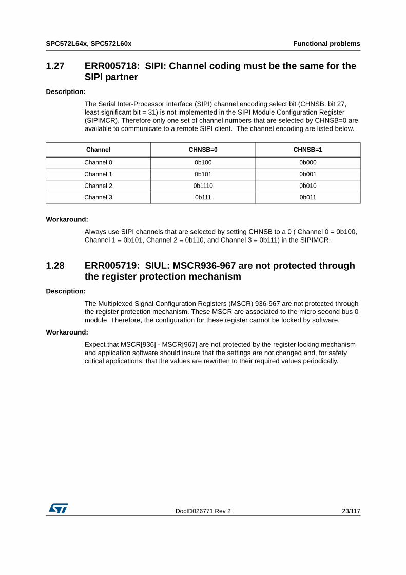
1.27 ERR005718: SIPI: Channel coding must be the same for the SIPI partner
Description:
The Serial Inter-Processor Interface (SIPI) channel encoding select bit (CHNSB, bit 27, least significant bit = 31) is not implemented in the SIPI Module Configuration Register (SIPIMCR). Therefore only one set of channel numbers that are selected by CHNSB=0 are available to communicate to a remote SIPI client. The channel encoding are listed below.
Workaround:
Always use SIPI channels that are selected by setting CHNSB to a 0 ( Channel 0 = 0b100, Channel 1 = 0b101, Channel 2 = 0b110, and Channel 3 = 0b111) in the SIPIMCR.
1.28 ERR005719: SIUL: MSCR936-967 are not protected through the register protection mechanism
Description:
The Multiplexed Signal Configuration Registers (MSCR) 936-967 are not protected through the register protection mechanism. These MSCR are associated to the micro second bus 0 module. Therefore, the configuration for these register cannot be locked by software.
Workaround:
Expect that MSCR[936] - MSCR[967] are not protected by the register locking mechanism and application software should insure that the settings are not changed and, for safety critical applications, that the values are rewritten to their required values periodically.
Channel CHNSB=0 CHNSB=1
Channel 0 0b100 0b000
Channel 1 0b101 0b001
Channel 2 0b1110 0b010
Channel 3 0b111 0b011
Functional problems SPC572L64x, SPC572L60x
24/117 DocID026771 Rev 2
1.29 ERR005726: GTM: A CPU write to the BRIDGE_MODE register can result in blocking of the AEI configuration interface
Description:
(GTM-IP-132)
If the Generic Timer Module (GTM) Automotive Electronics Interface (AEI) bridge operates in Mask Write Response mode (MSK_WR_RESP=1 in GTM_BRIDGE_MODE register), a requested change of the bridge mode (BRG_MODE) can result in the blocking of the GTM's bus interface because the GTM bus interface does not issue an AEI_READY signal when the write is completed.
Workaround:
Ensure that any write to the GTM_BRIDGE_MODE register bit BRG_MODE which changes the mode of the bridge (ASYNC/SYNC or vice versa) is accompanied by a Bridge Reset (BRG_RST =1 in GTM_BRIDGE_MODE register).
1.30 ERR005749: SDADC: New conversion data is discarded if the overflow (DFORF) status bit is set
Description:
The Sigma-Delta Analog-to-Digital Converter (SDADC) stops filling the Converted Data Register (CDR) and FIFO (if enabled) when the FIFO overrun bit in the Status Flag Register (SFR[DFORF]) becomes set.
The SFR[DFORF] bit becomes set when a FIFO or CDR overflow condition occurs, and once this happens the SDADC stops filling the CDR and FIFO, causing new converted data results to be discarded until the software clears the overflow bit. After clearing the overflow, normal operation resumes.
Workaround:
If the Global DMA/Interrupt gating feature is not being used then the problem can be avoided by either of two methods.
1. If DMA is being used then continuously transferring the CDR or FIFO data via DMA will prevent overflows.
2. If DMA is not used then use an interrupt service routine (ISR) to clear the overflow bit (SFR[DFORF]) and empty the FIFO/CDR
If the Global DMA/Interrupt gating feature is being used then use an interrupt service routine at the start of the DMA gating window to clear the DFORF bit and empty the FIFO and CDR. This will resume normal filling of the CDR. or FIFO which should then be serviced using DMA or ISR for the duration of the gating window.
DocID026771 Rev 2 25/117
SPC572L64x, SPC572L60x Functional problems
105
1.31 ERR005860: DSPI: Timing does not match specification
Description:
The Deserial Serial Peripheral Interface (DSPI) AC Specifications are not met by the device.
Workaround:
Do not use DSPI communication line at maximum baud rate.
1.32 ERR005906: GTM: TOM and ATOM inter module triggers delay
Description:
(GTM-IP-134)The trigger signal between the Generic Timer Module (GTM) Timer Output Module (TOM) or ARU Connected TOM (ATOM) submodules (e.g. signal TOM_TRIG_[i]) can be stored in a register at the module output to break long combinational paths. When this store register in place, it results in a delay of one system clock period of the trigger signal.Between module instances TOM[i] / ATOM[i] and TOM[i+1] / ATOM[i+1], when there is a store register in the trigger path, this trigger is only recognized by the channel of TOM[i+1] / ATOM[i+1] if the channel is running from a source identical to the system clock (i.e. the selected Clock Management Unit Fixed Frequency Clock (CMU_FXCLKx) or Clock Management Unit Clock (CMU_CLKx) period is the system clock (SYS_CLK) ÷ 1). If a lower frequency is chosen to clock the TOM[i+1] / ATOM[i+1] channel, the trigger is not recognized.
Workaround:
TOM Workaround 1:When there is a register in the trigger path between TOM[i] and TOM[i+1], the channel of TOM[i+1] that should be triggered has to use a clock of period identical to SYS_CLK period. The configuration of the TOM outputs differs between devices, in some cases each TOM has the save trigger register, in some devices every second TOM module has the register. Check the GTM specification for the configuration applicable to the device in use.TOM Workaround 2:On TOM[i+1] configure a redundant channel to trigger another channel of TOM[i+1] as it was configured on TOM[i] to trigger the other channel. Then start TOM[i] and TOM[i+1] synchronously by using the Time Base Unit (TBU) comparator of the TOM Global Control (TGCx) unit (TOM[i]_TGC[y]_ACT_TB register).ATOM Workaround 1:When there is a register in the trigger path between ATOM[i] and ATOM[i+1], the channel of ATOM[i+1] that should be triggered has to use a clock of period identical to SYS_CLK period. The configuration of the ATOM outputs differs between devices, in some cases each ATOM has the save trigger register, in some devices every second ATOM module has the register. Check the GTM specification for the configuration applicable to the device in use.ATOM Workaround 2:On ATOM[i+1] configure a redundant channel to trigger another channel of ATOM[i+1] as it was configured on ATOM[i] to trigger the other channel. Then start ATOM[i] and ATOM[i+1]
Functional problems SPC572L64x, SPC572L60x
26/117 DocID026771 Rev 2
synchronously by using the Time Base Unit (TBU) comparator of the ATOM Global Control (AGC) unit (ATOM[i]_AGC_ATC_TB register).
1.33 ERR005907: GTM: TIM ACB word is incorrect in the case of timeout detection
Description:
(GTM-IP-135)
When the timeout detection unit (TDU) of a Generic Timer Module (GTM) Timer Input Module (TIM) channel is enabled (TIM[i]_CH[n]_CTRL[TOCTRL] != '00') and the ARU routing for this channel is enabled (TIM[i]_CH[n]_CTRL[ARU_EN] = '1') the ARU Control Bits (ACB) presented to the Advanced Routing Unit (ARU) may indicate a timeout with an overflow of the General Purpose Registers (GPRz=0/1), ACB2=1 and ACB1=1 respectively, although no measurement cycle has finished (e.g. no signal change at the input port).
This situation occurs when two or more successive timeout events occur without any ARU read access from the TIM data's destination. The ARU connected data destination of the TIM channel will detect a valid measurement cycle after a timeout event although only a timeout event occurred.
Workaround:
To reliably detect that a measurement cycle finished after a timeout event, the GTM should additionally route the edge counter via the ARU. Whenever the ARU destination detects a transfer with ACB2=1 and ACB1=1 but the edge counter value did not change since the last ARU transfer, the received ARU word should be treated as normal timeout event (ACB2=1 and ACB1=0).
This workaround can be applied directly in the MCS if the MCS is used as data destination. If FIFO is used as data destination, the workaround has to be implemented by SW.
1.34 ERR005947: SARADC: ADC may miss a GTM trigger pulse if width of pulse is less than 1 AD Clk cycle
Description:
The Successive Approximation Register Analog to Digital Converter (SARADC) may miss a trigger (and no conversions will be started) from the Generic Timer Module (GTM) if the pulse width from the GTM Timer Output Module (TOM) or Advanced Routing Unit (ARU) Connected TOM (ATOM) is less than one ADC clock. The GTM Counter Compare Unit registers (CM0/CM1) set the pulse width.
Workaround:
The GTM registers Counter Compare Unit registers (CM0 and CM1) should be appropriately programmed such that pulse width of trigger pulses is always greater than one (1) ADC clock cycle.
DocID026771 Rev 2 27/117
SPC572L64x, SPC572L60x Functional problems
105
1.35 ERR005962: MC_ME: Incorrect setting of ME_IMTS[S_MRIG] bit on illegal mode requests
Description:
The S_MRIG bit of the Invalid Mode Transition Status register (ME_IMTS) in the Mode Entry module (MC_ME) is supposed to be set only when a mode change request is ignored while a SAFE mode transition is in progress. However, incorrectly, it is also set when a mode change request is made to a mode other than DRUN while the device is in SAFE mode and the transition to SAFE mode has completed. The correct behavior in this case would be that the S_MRI bit gets set. The mode change request itself is correctly ignored, and the device stays in SAFE mode.
Workaround:
Software should treat the setting of the ME_IMTS[S_MRIG] bit after a mode change request when already in SAFE mode the same as the ME_IMTS[S_MRI] bit being set. Whether the transition to SAFE mode has fully completed can be determined by comparing the MC_ME's Global Status register (ME_GS) content with that of its SAFE Mode Configuration register (ME_SAFE_MC).
1.36 ERR005978: MC_CGM: System clock dividers generate unaligned divided clocks when programmed back to back and when the first divider is configured for divide by 3
Description:
System clock dividers in the Clock Generation Module (MC_CGM) generate unaligned divided clocks when all the conditions below are met:
1. Dividers are configured back to back (without any delay in between)
2. The first divider to be programmed is in divide by 3 configuration
In such a scenario the divided system clocks are generated with unaligned active edges, which can lead to unpredictable behavior such as incorrect register and memory reads and writes.
Workaround:
Software should read the System Clock Divider Configuration registers (CGM_SC_DCn) after writing them. This ensures that back to back writes do not happen, and the condition required for the failure to occur is never met.
Functional problems SPC572L64x, SPC572L60x
28/117 DocID026771 Rev 2
1.37 ERR005994: FLASH: Prefetch mini-cache enable fields are configurable and default to disabled
Description:
The Flash prefetch mini-cache enable fields in the Platform Flash Configuration Registers (PFCR1[P0_BFEN] and PFCR2[P1_BFEN]) are configurable and default to disabled. Leaving the prefetch mini-cache enable field unchanged from their default states may result in lower lifetime performance when accessing the flash data and prevention of flash read disturb cannot be guaranteed. In the future, these bits will default to enabled and will not be changeable.
Workaround:
Set PFCR1[BFEN] and PFCR2[BFEN] during initialization, then do not modify this setting.
1.38 ERR006026: DSPI: Incorrect SPI Frame Generated in Combined Serial Interface Configuration
Description:
In the Combined Serial Interface (CSI) configuration of the Deserial Serial Peripheral Interface (DSPI) where data frames are periodically being sent (Deserial Serial Interface, DSI), a Serial Peripheral Interface (SPI) frame may be transmitted with incorrect framing.
The incorrect frame may occur in this configuration if the user application writes SPI data to the DSPI Push TX FIFO Register (DSPI_PUSHR) during the last two peripheral clock cycles of the Delay-after- Transfer (DT) phase. In this case, the SPI frame is corrupted.
Workaround:
Workaround 1: Perform SPI FIFO writes after halting the DSPI.
To prevent writing to the FIFO during the last two clock cycles of DT, perform the following steps every time a SPI frame is required to be transmitted:
Step 1: Halt the DSPI by setting the HALT control bit in the Module Configuration Register (DSPI_MCR[HALT]).
Step 2: Poll the Status Register's Transmit and Receive Status bit (DSPI_SR[TXRXS]) to ensure the DSPI has entered the HALT state and completed any in-progress transmission. Alternatively, if continuous polling is undesirable in the application, wait for a fixed time interval such as 35 baud clocks to ensure completion of any in-progress transmission and then check once for DSPI_SR[TXRXS].
Step 3: Perform the write to DSPI_PUSHR for the SPI frame.
Step 4: Clear bit DSPI_MCR[HALT] to bring the DSPI out of the HALT state and return to normal operation.
Workaround 2: Do not use the CSI configuration. Use the DSPI in either DSI-only mode or SPI-only mode.
Workaround 3: Use the DSPI's Transfer Complete Flag (TCF) interrupt to reduce worst-case wait time of Workaround 1.
Step 1: When a SPI frame is required to be sent, halt the DSPI as in Step 1 of Workaround 1 above.
DocID026771 Rev 2 29/117
SPC572L64x, SPC572L60x Functional problems
105
Step 2: Enable the TCF interrupt by setting the DSPI DMA/Interrupt Request Select and Enable Register's Transmission Complete Request Enable bit (DSPI_RSER[TCF_RE])Step 3: In the TCF interrupt service routine, clear the interrupt status (DSPI_SR[TCF]) and the interrupt request enable (DSPI_RSER[TCF_RE]). Confirm that DSPI is halted by checking DSPI_SR[TXRXS] and then write data to DSPI_PUSHR for the SPI frame. Finally, clear bit DSPI_MCR[HALT] to bring the DSPI out of the HALT state and return to normal operation.
1.39 ERR006033: CCCU: software reset may trigger a second interrupt
Description:
When a software reset is issued to the Clock Calibration on CAN Unit (CCCU) by setting to '1' the Software Reset bit of the Calibration Configuration register (CCFG[SWR]=1) while the CCCU is in Not_Calibrated state (field Calibration State (CALS) is '00' in the Calibration Status Register (CSTAT))
AND when at the same time the connected M_(TT)CAN signals successful reception of a CAN message by activating the message receive line, two pulses may be generated on the calibration state change line.
If an interrupt is enabled as reaction to a calibration state change, this may trigger a second interrupt for the same event.
Workaround:
Ignore Calibration State Changed output/interrupt in case of a software reset.
1.40 ERR006041: GTM: TOM and ATOM in center aligned PWM configuration, with CM0=0 or CM0=1 on a triggered channel does not output correct waveform
Description:
(GTM-IP-136)
When a Generic Timer Module (GTM) Timer Output Module (TOM) or Advanced Routing Unit Connected TOM (ATOM) channels counter, CN0, is reset by the trigger of a preceding channel (RST_CCU0=1 in the channel control register TOM[i]_CH[x]_CTRL / ATOM[i]_CH[x]_CTRL) and a 100% or 0% duty cycle Pulse Width Modulation (PWM) is requested by configuring CM0=0 (compare register 0) (0%) or CM1(compare register 1)>=CM0 (100% when CM0=1) no edge is generated.
In the configuration where CM0=0, no edge is generated because counter CN0 is not running after the reset event.
In the case when CM0=1 and CM1>=CM0, no edge is generated even though counter CN0 is running.
Functional problems SPC572L64x, SPC572L60x
30/117 DocID026771 Rev 2
Workaround:
Instead of using the configuration CM0=0 and CM1>0, use the configuration CM1=0 and CM0>CM1 and invert value of Signal Level (SL) bit to generate 0% / 100% PWM signals.
1.41 ERR006042: SARADC: extra clock cycle when chaining conversion
Description:
The Successive Approximation Register Analog to Digital Conversion (SARADC) requires one (1) additional Tck cycle to complete the conversion when chaining to the next channel. The actual formula becomes:
Tconv = Tprechg+Tsample+Teval + 1*Tck
= PRECHG*Tck+INPSAMP*Tck+25*Tck + 1*Tck
Within the reference manual, conversion time is specified as below:
Tconv = Tprechg+Tsample+Teval
= PRECHG*Tck+INPSAMP*Tck+25*Tck with following naming convention:
Tck: SAR ADC clock cycle
Tprechg: precharge period, as defined in CTRn[PRECHG]
Tsample: sampling period, as defined in CTRn[INPSAMP]
Teval: fixed period of 25 SARADC clock cycles (Tck)
Workaround:
Expect one additional clock cycle to be required in case of chained conversion.
1.42 ERR006072: GTM: Wrong PSTC/PSSC value after initialization and restart of DPLL
Description:
(GTM-IP-138)
Before the First Trigger is Detected (FTD = 0 in DPLL_STATUS register) after the Generic Timer Module (GTM) Digital Phase Lock Loop (DPLL) has been initialized, the value of the Actual Calculated Position Stamp in the TRIGGER Register (PSTC) should be set equal to the Measured Position Stamp of the Last TRIGGER Input Register (PSTM). The PSTC value is not initialized with PSTM value on 1st TRIGGER edge. Once the First Trigger is Detected (FTD = 1), the PSTC is not updated with PSTM value.
After each DPLL stop and restart sequence, the PSTC continues counting without any synchronization to the current position.
This also applies to the Actual Calculated Position Stamp of STATE (PSSC) and Measured Position Stamp at Last STATE Input Register (PSSM).
DocID026771 Rev 2 31/117
SPC572L64x, SPC572L60x Functional problems
105
Workaround:
Write the PSTC and PSSC registers with the contents of the PSTM and PSSM registers via CPU during the DPLL initialization.
1.43 ERR006073: GTM: MCS channel might not be disabled by the MCU core
Description:
(GTM-IP-137)
When a Generic Timer Module (GTM) Multi Channel Sequencer (MCS) channel is requested to be disabled by the MCU's core through the GTM wrapper by clearing the channel enable bit (MCS[i]_CH[n]_CTRL.B.EN = 0x0), it is possible that the disable request is not executed by the MCS channel.
Workaround:
The MCU core should repeat the clearing of the Enable Channel bit (EN) of the MCS Channel Control register (MCS[i]_CH[x]_CTRL) in a loop until EN is cleared.
Repeat clearing the EN bit of the register MCS[i]_CH[x]_CTRL in a loop until it is cleared. For example:
while (MCS[i]_CH[n]_CTRL.B.EN == 1)
{
MCS[i]_CH[n]_CTRL.B.EN = 0x0;
}
Note: This loop could take the whole duration of an Advanced Routing Unit (ARU) round trip time, if an ARU transfer is currently running, or the duration of a Wait Until Register Match (WURM) suspension time, if a WURM is currently suspending the channel.
1.44 ERR006077: MC_CGM: Value of CGM_SC_SS[SWTRG] may be incorrect after power-on reset
Description:
After power-on reset, the Switch Trigger cause (SWTRG) field of the System Clock Select Status register (CGM_SC_SS) in the Clock Generation Module (MC_CGM) may incorrectly contain the value 0b000 (“reserved”) instead of the expected value of 0b100 (“switch to 16 MHz internal RC oscillator (IRCOSC) due to SAFE mode request or reset succeeded”). The system clock is still correctly sourced by the IRCOSC as expected.
Workaround:
Software should interpret CGM_SC_SS[SWTRG] = 0b000 right after a power-on reset as "switch to 16 MHz internal RC oscillator due to SAFE mode request or reset succeeded”. In all other cases, it should be interpreted as “reserved”.
Functional problems SPC572L64x, SPC572L60x
32/117 DocID026771 Rev 2
1.45 ERR006080: LINFlexD: HRF flag in LINSR (LIN Status Register) is not cleared by hardware
Description:
The Header Received Flag (HRF) in Local Interconnect Network (LIN) Status Register (LINSR) is not cleared by Hardware after the complete frame is received. Due to this, an erroneous transmission of data might begin again.
Workaround:
HRF should be cleared by software only as soon as it is set.
1.46 ERR006082: LINFlexD: LINS bits in LIN Status Register(LINSR) are not usable in UART mode.
Description:
When the LINFlexD module is used in the Universal Asynchronous Receiver/Transmitter (UART) mode, the LIN state bits (LINS3:0]) in LIN Status Register (LINSR) always indicate the value zero. Therefore, these bits cannot be used to monitor the UART state.
Workaround:
LINS bits should be used only in LIN mode.
1.47 ERR006084: PFLASH: SAFE_CAL feature allows calibration remap when Word 2 of a redundant pair is mismatched.
Description:
When any of the 3 Calibration Remap Descriptor Words (CRDn.WORD0...2) of a redundant CRD pair are not equal, the Safe Calibration (SAFE_CAL) feature disables calibration remap. This feature works for CRDn.WORD0 and CRDn.WORD1 mismatches. However, a mismatch in CRDn.WORD2 incorrectly keeps calibration remap enabled.
Workaround:
Do not use Flash overlaying in a safety-relevant way in production series cars.
1.48 ERR006087: MC_RGM: Reset event during mode transition causes chip to remain in reset
Description:
If a reset due to any 'destructive' reset event, “functional” reset event, external Power On Reset pin (PORST) assertion, or External functional reset pin (ESR0) assertion occurs coincidental with a mode change request triggered via the Mode Control register (ME_CTL) in the Mode Entry module (MC_ME), the MCU enters reset but may not exit reset. The time window during which the reset event must occur for this to happen is one system clock period, so the likelihood is extremely small. However, if it does happen, the only way to recover the chip is through a power-on reset by powering down the chip and then powering it up again.
DocID026771 Rev 2 33/117
SPC572L64x, SPC572L60x Functional problems
105
The time window during which a reset event occurring can cause this problem exists only if
the system clock source is changed via the SYSCLK field in the target Mode Configuration register (ME_"target_mode"_MC) and, in the same mode change request, the new system clock source is being turned from off to on via the ME_"target_mode"_MC["clock_source"ON] bit.
Workaround:
Perform a power cycle of the MCU to recover from this event. If this is not possible in all cases, external circuitry should be installed that uses a General Purpose Output to hold off all external resets.
1.49 ERR006088: MC_RGM: Requested peripheral reset not applied as expected
Description:
If a peripheral is requested to be put into reset by writing a 0b1 to the appropriate bit of one of the Peripheral Reset registers (RGM_PRSTn) in the Reset Generation Module (MC_RGM), and then shortly thereafter requested to exit reset by writing a 0b0 to the same bit, it may occur that the peripheral in question does not actually get reset.
In addition, attempting to access any of the Peripheral Reset Status registers (RGM_PSTATn) in the MC_RGM, which are intended to allow software to see if a peripheral is currently in reset, results in an access error.
Workaround:
Software should wait long enough between the peripheral reset request and peripheral reset exit request to allow at least three peripheral clock cycles to occur in between. If a peripheral has multiple clocks, then the clock with the lowest frequency should be used as a gauge.
Software should also check whether the peripheral was actually reset by afterwards reading various registers and comparing them with their expected reset values.
Software should not try to access the RGM_PSTATn register locations.
1.50 ERR006090: MC_CGM: CGM_SC_DIV_RC register does not exist
Description:
The System Clock Divider Ratio Change register (CGM_SC_DIV_RC) in the Clock Generation Module (MC_CGM) does not exist. Accessing this register's location results in an access error.
Workaround:
Software should not try to access the CGM_SC_DIV_RC register location.
Functional problems SPC572L64x, SPC572L60x
34/117 DocID026771 Rev 2
1.51 ERR006091: SDADC/SARADC: coupling current on ADC pin may be present when S/D are not enabled
Description:
The analog pins associated with the Analog to Digital Delta/Sigma Converter (SDADC) are shared with the Successive Approximation Register Analog to Digital Converter (SARADC). When none of the SDADC modules are enabled, a current injection (greater than 1mA) on one of the pins may generate a extra leakage (100nA at 25c) on the other SDADC pins.
Workaround:
In case one of these shared pins is to be used as a SARADC channel, at least one SDADC module should be enabled.
A SDADC_x module is enabled by setting (writing '1') the enable field (EN) of its Module Configuration Register (MCR) (SDADC_x_MCR[EN)=1).
In addition, to avoid any influence on input pins assigned to the chosen SDADC_x module, the Analog Channel Selection field (ANCHSEL) should be set to 0b100 (SDADC_x_CSR[ANCHSEL]=4) in order to connect the internal negative reference as input of the converter.
1.52 ERR006099: SDADC: FIFO data corruption is possible in certain configurations of the FIFO threshold
Description:
The Sigma Delta Analog to Digital Converter (SDADC) does not support a First-In-First-Out (FIFO) flush option. This can result in the FIFO having older data if the FIFO control register (FCR) FIFO threshold [FTHLD] value is programmed for a number of datawords less than the maximum depth of the FIFO, as indicated by the read only bits FCR[FSIZE].
In this configuration, if DMA (Direct Memory Access) is enabled and a DMA request is generated on a FIFO full condition (the number of written datawords is equal to the FTHLD value), once the DMA transfer for FTHLD datawords is completed, the FIFO can still contain some unread datawords (FSIZE-FTHLD maximum). This unread data will be present even after the SDADC is disabled by clearing the SDADC module configuration register enable bit (MCR[EN]), or after a change of channel selection by writing the channel selection register (CSR) analog channel select bitfield [ANCHSEL] with a new channel for a new conversion.
This condition can result in a DMA transfer on the next DMA request of a mix of older data (corresponding to the previously selected channel) and new data (corresponding to the next channel selection).
Workaround:
Software should read and discard all the older data from the FIFO before starting any new conversion.
DocID026771 Rev 2 35/117
SPC572L64x, SPC572L60x Functional problems
105
1.53 ERR006349: LINFlexD: Possibility of incorrect break delimiter length in header by LIN master
Description:
When the Local Interconnect Network module (LINFlexD) is used in LIN mode, the length of the break field delimiter can be configured to either 1 or 2 bits using the Two Bit Delimiter bit (TBDE) of the LIN Control Register 2 (LINCR2).
Once LINCR2[TBDE] has been set (selecting 2 bits length), it is no longer possible to clear it (selecting 1 bit length).
This may result in LIN master always transmitting the header with two bits of delimiter in the break field.
Workaround:
To clear LINCR2[TBDE] field, a system reset has to be performed.
1.54 ERR006350: LINFlexD: WLS feature cannot be used in buffered mode.
Description:
The LINFlex module may not operate correctly if the Special Word Length (WLS) for enabling 12-bit data length is selected in the Universal Asynchronous Receiver/Transmitter (UART) Mode Control Register (UARTCR) and configured in the transmit buffered mode.
Workaround:
When WLS mode is required, always use the First In, First Out (FIFO_ mode of the UART LINFLEX module by setting the Transmit FIFO/Buffer mode bit of the UARTCR (UARTCR[TFBM]=1).
1.55 ERR006361: INTC: Interrupt Priority Inversion can occur on a write to INTC_CPRn[PRI]
Description:
When the External Interrupt Enable (EE) field of the core's Machine Status Register (MSR) is 0 (MSR[EE]=0) and a write occurs to the Priority (PRI) field of the Interrupt Controller's (INTC) Current Priority Register for Processor n (INTC_CPRn) the INTC uses the previous INTC_CPRn[PRI] value when re-evaluating the interrupt requests instead of the one just written. This means that a pending interrupt prior to the store of a higher priority value to the INTC_CPRn[PRI] could be serviced, known as a priority inversion.
Workaround:
Software workaround is to write to the INTC_CPRn[PRI] twice in a row.
Functional problems SPC572L64x, SPC572L60x
36/117 DocID026771 Rev 2
1.56 ERR006369: PAD_RING: Pull current does not meet updated specification
Description:
The weak pull current of the general purpose input/output port are below the value currently specified in the datasheet. The current in the datasheet is defined with respect to the threshold of the input buffer: input voltage (Vin) = Voltage input High (Vih) for pull-up, Vin = Voltage Input Low (Vil) for pull- down.
As implemented, the weak pull current is defined with respect to supply: Vin= 0.0V for weak pull-up, Vin=VDD_HV for weak pull-down. Weak pull current is thus defined as below:
The pull-up current is in the range 25uA-100uA for Vin = 0.0V with VDD_HV_IO supply in the range 4.0V < VDD_HV_IO< 5.9V.
The pull-down current is in the range 30uA-80uA for Vin = VDD_HV_IO with VDD_HV_IO supply in the range 4.0V < VDD_HV_IO< 5.9V
Workaround:
If need, application should implement external resistance to increase pull-up/pull-down current as required
1.57 ERR006383: SIPI: 16 bit writes/reads may access incorrect addresses
Description:
16-bit read and writes operations that are not on a 32-bit word boundary alignment will not operate correctly in the Serial Interprocessor Interface. 16-bit accesses to any address that matches 0x2, 0x6, 0xA or 0xE will access an incorrect address.Therefore writes will be to an incorrect address and reads will return data from the wrong address. 16-bits accesses to addresses matching 0x0, 0x4, 0x8, and 0xC will operate properly.
Workaround:
Only use 32- or 8-bit write/reads instead of 16-bit for all SIPI transactions.
DocID026771 Rev 2 37/117
SPC572L64x, SPC572L60x Functional problems
105
1.58 ERR006409: GTM: ATOM Force Update does not activate a comparison when in SOMC mode
Description:
(GTM-IP-139)
When the Generic Timer Module (GTM) ARU Connected Timer Output Unit (ATOM) is configured in Signal Output Mode Compare (SOMC) mode, with the Advanced Routing Unit (ARU) Enabled, and if no comparison is active (no valid data was received by ARU, ATOM[i]_CH[x]_STAT.B.DV = 0) a Force Update Request can cause the ATOM to remain in a state waiting for the update event to happen.
A Force Update is requested by first setting CPU Write Request field (WR_REQ) in ATOM[i]_CH[x]_CTRL, then updating the Shadow Counter Registers (ATOM[i]_CH[x]_SRx) and optionally the ATOM Mode Control Bits (ACB) in ATOM[i]_CH[x]_CTRL, and finally updating the Counter Registers (ATOM[i]_CH[x]_CMx) via a Forced Update (ATOM[i]_TGCx_FUPD_CTRnL = 0b11).
Under the above conditions:
The registers CMx are updated correctly but no new comparison is activated.
The ACBO bits are erroneously not cleared.
The ARU read request is canceled because of WR_REQ=1.
Workaround:
After the Forced Update, re-write the desired values to CM0 or CM1 to activate the comparison and to reset the ACBO bits.
1.59 ERR006410: GTM: Write to ATOM_CH_CTRL sets WRF if CCU0 compare match has already occurred, but CCU1 compare match is pending, in ATOM SOMC mode
Description:
(GTM-IP-140)
When the Generic Timer Module (GTM) ARU Connected Timer Output Unit (ATOM) is configured in Signal Output Mode Compare (SOMC) mode, with the Advanced Routing Unit (ARU) Enabled, the capture/compare strategy is 'Serve Last' (ATOM[i]_CH[x]_CTRL.B.ACB42 = 0b1xx), with Counter Compare Unit 0 (CCU0) matched but the CCU1 match is pending, a write access to the ATOM Channel Control register (ATOM[i]_CH[x]_CTRL) will set the “Write Request of CPU Failed for the Last Update” (WRF) field in the Channel Status Register (ATOM[i]_CH[x]_STAT) independently of the status of the CPU Write Request Bit for Late Compare field (WR_REQ) in ATOM[i]_CH[x]_CTRL.
Workaround:
If ATOM[i]_CH[x]_CTRL is written during an active 'Serve Last' comparison without the intention of setting WR_REQ, write to ATOM[i]_CH[x]_CTRL and then reset/clear WRF in ATOM[i]_CH[x]_STAT by writing a '1'.
Functional problems SPC572L64x, SPC572L60x
38/117 DocID026771 Rev 2
1.60 ERR006411: GTM: Incorrect Input Signal Characteristics when the TIM channel is in TIEM, TPWM, TIPM, TPIM or TGPS mode, when ECNT is selected as the captured GPRi value.
Description:
(GTM-IP-141)
When a Generic Timer Module (GTM) Timer Input Module (TIM) channel captures a valid rising edge event at TIM[i]_CH[x]_FOUT (post filtering) in TIM Input Event Mode (TIEM), TIM PWM Measurement Mode (TPWM), TIM Input Prescaler Mode (TIPM), TIM Pulse Integration Mode (TPIM) or TIM Gated Periodic Sampling Mode (TGPS), the captured values of the Edge Counter (TIM[i]_CH[x]_ECNT) to the General Purpose Registers (TIM[i]_CH[x]_GPRi) are incorrect. The captured value will be ECNT+2; bit 0 (signal level) will be 0 (Falling Edge). The correct operation would be to capture ECNT+1; bit 1 (signal level) would be 1 (Rising Edge).
This leads to an inconsistency between the ARU signal level bit, bit 0 of the ARU word which shows the captured ECNT value, and TIM[i]_CH[x]_GPRi which shows an inconsistency when comparing GPRi [bits 31:24] to ECNT [bits 7:0].
Workaround:
When using the TIMs captured data the correct data can be reconstructed by:
if ARU_SIGNAL_LEVEL ==1 and ARU_DATA[0] == 0 the ARU_DATA = ARU_DATA -1;
When reading TIM[i]_CH[x]_GPRi by the data can be corrected as long as there is no GPR overflow and no new edge by:
if TIM[i]_CH[x]_GPRi[24] == 1 and TIM[i]_CH[x]_GPRi[0] == 0 then TIM[i]_CH[x]_GPRi[23:0] = TIM[i]_CH[x]_GPRi[23:0] -1;
1.61 ERR006412: GTM: Incorrect Input Signal Characteristics when the TIM channel is in TBCM mode and ECNT is selected as the captured GPR0 value.
Description:
(GTM-IP-142)
When a Generic Timer Module (GTM) Timer Input Module (TIM) channel captures an input pattern match condition in TIM Bit Compression Mode (TBCM), the values captured by the General Purpose Register TIM[i]_CH0_GPR0 are incorrect under the condition EGPR0_SEL=1 with GPR0_SEL= 0 (use ECNT as input).
Starting at t=0 with counter value ECNT(t=0), the captured values of two consecutive edges can be ECNT(t=0)+2 followed by ECNT(t=0)+2 instead of ECNT(t=0)+1 followed by ECNT(t=0)+2. The captured ECNTs do not increment by 1 as expected, and reading TIM[i]_CH0_GPR0 shows an inconsistency when comparing ECNT [bits 31:24] to GPR0 [bits 7:0].
DocID026771 Rev 2 39/117
SPC572L64x, SPC572L60x Functional problems
105
Workaround:
Ignore the captured data via the Advanced Routing Unit (ARU) and construct the edge count value with an independent Multi Channel Sequencer (MCS) counter which increments on each ARU transfer, or when reading TIM[i]_CH0_GPR0 use only TIM[i]_CH0_GPR0[31:24] as EDGE counter; do not use TIM[i]_CH0_GPR0[23:0].
1.62 ERR006424: LINFlexD: During reception of data, the first packet received could get lost
Description:
During reception of data by the Local Interconnect Network (LIN) module (LINFlexD), the data buffer pointer may increment one clock cycle before the data is received. Thus, the buffer location where data is intended to be written gets skipped and received data is written at an incorrect location.
The issue has only a low probability of occurrence, but could occur in both LIN and Universal Asynchronous Receiver/Transmitter (UART) modes.
Workaround:
The data buffer must be reset prior to each packet reception and the LINFlexD should only receive one non-zero data packet at a time.
Completion of data reception is indicated by Data Reception Completed Flag in the LIN status register (LINSR[DRF] = 1), or UART status register (UARTSR[DRF] = 1), or by the Direct Memory Access signal (dma_ipd_complete_tx) signal being set in the LIN buffer, UART buffer, and UART FIFO modes respectively. After one of this bits is set, non-zero data read from the data buffer is the expected received data.
1.63 ERR006427: LINFlexD: Communication failure when LIN timer is used in Output Compare mode
Description:
In the Local Interconnect Network Module (LINFlexD), the LIN state machine can be reset to the IDLE state on a timeout event, setting the Idle on timeout bit (IOT) bit of the LIN Time-Out Control Status Register (LINTCSR).
If the Timeout counter mode is set as Output compare (LINTCSR[MODE]=1), even if the Idle on Timeout bit is set (LINTCSR[IOT]=1), the LIN state machine does not move to IDLE state on timeout event.
Thus, further incoming data would not be interpreted correctly leading to communication failure.
Workaround:
The LIN state machine can be reset to the IDLE state on timeout event only using "LIN mode" as the timeout counter mode (LINTCSR[MODE] =0).
Functional problems SPC572L64x, SPC572L60x
40/117 DocID026771 Rev 2
1.64 ERR006428: LINFlexD: Data reception could terminate abruptly in LIN Slave mode when Time-out counter mode is enabled
Description:
When the Local Interconnect Network module (LINFlexD) is used in LIN Slave mode, and in the LIN Time-Out Control Status Register (LINTCSR) the time-out counter mode is configured to LIN mode (LINTCSR[MODE]=0), the Output Compare value 2 in LIN Output Compare Register (LINOCR[OC2]) is loaded by hardware to monitor the response duration.
This loaded value may be incorrect and may lead to setting the Output Compare Flag in the LIN Error Status register (LINESR[OCF]) after which data reception is terminated by the LIN slave.
Workaround:
Use the LINFlexD in LIN Slave mode with time-out control disabled in the LIN Time-out Control Status register (LINTCSR[TOCE]=0).
1.65 ERR006477: RGM: minimum PORST pulse is not guaranteed
Description:
When a destructive reset is triggered internal to the device by the Reset Generation Module (RGM), the bidirectional Power On Reset signal (PORST) is asserted. The PORST reset pulse width driven by the device may be lower than the specified 5µs and could be as short as 0.5µs. This pulse may not be visible depending on external circuitry configuration.
Workaround:
Use the External functional reset with Schmitt trigger (ESR0) signal to externally monitor the internal reset status.
DocID026771 Rev 2 41/117
SPC572L64x, SPC572L60x Functional problems
105
1.66 ERR006528: PAD_RING: LVDS cannot be enabled for DSPI_4 by configuring SSS bit field
Description:
Deserial Serial Peripheral Interface module 4 (DSPI_4) Microsecond Bus Serial Data and Clock Low- Voltage Differential Signaling (LVDS) functionality cannot be enabled on the PD[0]/PD[1] and PD[2]/PD[3] pins respectively by configuring the SSS (Source Signal Select) field of the System Integration Unit Lite2 (SIUL2) Multiplexed Signal Configuration Register (MSCR) 48 to 51 (MSCR48, MSCR49, MSCR50 and MSCR51) to 0b0010. This configuration has no effect and the LVDS pads remain disabled and will be in high impedance.
Workaround:
To enable the LVDS functionality, the Output Edge Rate Control (OERC) bit field of the SIUL2_MSCR50 must be used instead. Normally this 2-bit field specifies the driver strength of the associated pin: 0b00 = weak, 0b01 = medium, 0b10 = strong, 0b11 = very strong. In this case, the most significant bit is used to configure the driver strength: 0b0 = weak, 0b1 = very strong, while the least significant bit is used to configure the pads to LVDS or single ended: 0b0 = single ended, 0b1 = LVDS. In addition, the SSS field of the SIUL2_MSCR50 must be set to 0b0000.
1.67 ERR006538: LINFlexD: Stop mode request may be ignored if requested before the end of a frame
Description:
The LINFlexD module fails to enter stop mode when the stop mode request is issued before the second data byte of an ongoing frame transfer.
User requests stop mode by setting the appropriate bit of the Peripheral Control Register of the Mode Entry Module (ME_PCTLx).
Workaround:
If a LIN transmission/reception is in progress, wait until it reaches the frame boundary (complete current frame transfer) before sending a request to enter in stop mode.
1.68 ERR006552: MC_RGM: Reset event during mode transition causes chip to remain in reset
Description:
If a reset due to any 'destructive' reset event, 'functional' reset event, external Power On Reset pin (PORST) assertion, or External functional reset pin (ESR0 or RESET, depending on the MCU) assertion occurs coincidental with a mode change request triggered via the Mode Control register (ME_CTL) in the Mode Entry module (MC_ME), the MCU enters reset but may not exit reset. The time window during which the reset event must occur for this to happen is one system clock period, so the likelihood is extremely small. However, if it does happen, the only way to recover the MCU is through a power-on reset by powering down the device and then powering it up again.
Functional problems SPC572L64x, SPC572L60x
42/117 DocID026771 Rev 2
Workaround:
Perform a power cycle of the MCU to recover from this event. If this is not possible in all cases, external circuitry should be installed that uses a General Purpose Output to hold off all external resets during mode changes.
1.69 ERR006597: SRX: Pad input low level threshold (Vil) variation is not guaranteed to remain within +/-50mV on 1ms window
Description:
The Single Edge Nibble Transmission (SENT) specification requires drift on the low threshold of its input buffer (Vil) to be less than 50mV during a 1ms window. However, noise, linked to activity on pads in the neighborhood of the SENT interface, can create a local voltage drop on the VSS_HV_IO_MAIN/VDD_HV_IO_MAIN leading to up to 200mV of Vil drift when the pins are configured in Automotive level configuration. The Input Level Select (ILS) bits in the Multiplexed Signal Configuration Register (MSCR) select the pin voltage levels. The SENT interface full functionality may not be guaranteed if supply segment associated with the SENT interface is using more of than 25% of the segment capability, as defined in the datasheet IO signal table addendum.
Workaround:
Ensure activity on the power supply segment is limited to 25% of the maximum if the SENT interface must be used.
1.70 ERR006638: PASS: Incorrect Censor reset value
Description:
In the Device Configuration Format (DCF) Records, the reset value for the censorship client has the lower 16-bit value configured to 0x55AA. For the Password and device security module (PASS), this value means the device is not censored out of reset while the default state of the device should be censored, but allowing access to the device via a debugger/flash programmer.
Workaround:
In order to have the device censored out of reset, add a DCF record setting the data for the censorship client to any 32-bit value different from 0xUUUU55AA (only the lower 16 bits are considered).
DocID026771 Rev 2 43/117
SPC572L64x, SPC572L60x Functional problems
105
1.71 ERR006639: GTM: A compare match event does not clear WR_REQ when ATOM is in SOMC mode
Description:
(GTM-IP-146)
If a Generic Timer Module (GTM) ARU Connected Timer Output Module (ATOM) channel is operating in Signal Output Mode Compare (SOMC) mode, with the Advanced Routing Unit (ARU) enabled and a late compare register update is requested by the CPU by setting WR_REQ (CPU Write request bit for late compare register update in ATOM[i]_CH[x]_CTRL), a late update of the Counter Compare Unit (CCU0/1) Compare registers (CM0/CM1) and/or the compare strategy (i.e. ARU Control Bits (ACB) bits altered) is successfully done, but after final compare match the WR_REQ bit is not reset. As a result no new ARU read request is set up after final compare match.
Workaround:
CPU should clear WR_REQ by software after the late update.
1.72 ERR006640: GTM: Valid edge after Timeout event ignored by TIM
Description:
(GTM-IP-150)
When a Generic Timer Module (GTM) Timer Input Module (TIM) timeout event triggers an Advanced Routing unit (ARU) write request with timeout information “timeout detected without valid edge” (ARU Control Bit 2 (ACB2)=1 and ACB1=0), and this request is acknowledged by the ARU at the same time as a new valid edge occurs, the valid edge is neither acknowledged by setting the bits ACB2=1 and ACB1=1 (timeout detected with subsequent valid edge detected) within the acknowledged transfer nor acknowledged by setting up a subsequent ARU write request for the new valid edge with ACB2=0 and ACB1=0 (valid edge detected).
Workaround:
The workaround for this issue requires an additional plausibility check within the Multi Channel Sequencer (MCS) or CPU via FIFO:
Step 1) store the received data (ARUDATA(47:0)) and ACB0 in temporary variables.
Step 2) if an ARU transfer with ACB2=1 and ACB1=0 is received also check whether the previously received ARUDATA(47:0) and ACB0 values are the same:
If they are not the same values then a timeout with subsequent valid edge has occurred, which means ACB1 must be corrected to 1.
Functional problems SPC572L64x, SPC572L60x
44/117 DocID026771 Rev 2
1.73 ERR006642: GTM: THVAL not available immediately after inactive trigger in DPLL
Description:
(GTM-IP-152)
The Generic Timer Module (GTM) Digital PLL (DPLL) Measured TRIGGER hold time value (THVAL) is calculated correctly for each INVALID trigger slope, but this value is only stored into the THVAL memory location in RAM Region 1a with every new ACTIVE edge of the trigger signal.
Workaround:
If the THVAL value is needed immediately with the inactive trigger edge it is necessary to calculate the THVAL value by using Timer Input Module Channels 0/1 (TIM_CH0/1) to obtain the active and inactive slopes in TIM input event mode (TIEM). With these timestamps the CPU is able to calculate the time span.
1.74 ERR006643: GTM: Incorrect timestamp captured in CNTS when TIM operates in TPWM or TPIM modes if CMU_CLK is not equal to system clock
Description:
(GTM-IP-153)
When a Generic Timer Module (GTM) Timer Input Module (TIM) channel operates in the following configuration, the Timebase Unit Channel 0 (TBU_TS0) value is not captured correctly in to the counter register CNTS:
PWM Measurement Mode (TPWM) or Pulse Integration Mode (TPIM) and
TBU_TS0 selected as the input to CNTS (CNTS_SEL = 1 in TIM[i]_CH[x]_CTRL) and
Selected clock (CMU_CLKn) of the TIM channel is not the same frequency as the system clock.
Workaround:
Configure the TIM channel to operate on a CMU_CLK (Divider =1) which is identical to the system clock when TBU_TS0 is to be captured in TPWM or TPIM modes.
1.75 ERR006644: GTM: Incorrect duty cycle in TOM PCM mode
Description:
(GTM-IP-154)
The Generic Timer Module (GTM) Timer Output Module (TOM) duty cycle output in Pulse Count Modulation (PCM) mode is always one count less than the configured value in the Compare Match 1 (CM1) register. For example, if the value 1 is written to CM1, a duty cycle of 0% will be generated and if a duty cycle of 100% was configured by writing the maximum value (0xFFFF) in to the CM1 register, the resultant waveform would be a signal with duty cycle less than 100%. A value of zero in the CM1 register results in 100 duty cycle.
DocID026771 Rev 2 45/117
SPC572L64x, SPC572L60x Functional problems
105
Workaround:
Configure the CM1 value for the targeted duty cycle in the CM1 register with target duty cycle + 1.
To get 0% duty cycle, CM1 = 1.
To get 100% duty cycle, CM1 = 0 and CM0 = 0xFFFF. (Setting CM0 = 0x1000 and CM1 = 0xFFFF will also result in a duty cycle of 100%)
1.76 ERR006645: GTM: Clearing of DPLL PCM1/2 bits after the Missing Pulse Correction Values calculations delayed
Description:
(GTM-IP-158)
The Generic Timer Module (GTM) Digital PLL (DPLL) Pulse Correction Mode bits (PCM1/2 in DPLL_CTRL_1) are expected to be cleared after the Missing Pulse Correction Values (MPVAL1/2) are used to calculate the number of sub_incs for the next increment and to calculate the add_in values by the DPLL State Machine, however the PCM1/2 bit is transferred with an active edge into the dedicated shadow registers, but cleared some time later. If the PCM1/2 bits are written by the CPU in between the point of time of the transfer to the shadow register and the point of time were the PCM1/2 bits are cleared, the bits are cleared and never used.
Workaround:
Do not allow the CPU to write to the PCM1/2 bits until at least 750 system clocks have passed since the previous Trigger Active Slope Detected (TASI) interrupt. This time could be derived by an GTM resource like an ARU connected TOM (ATOM) channel.
1.77 ERR006720: SIUL2: Logic state of LVDS input pads cannot be read via GPDI registers.
Description:
When two adjacent pads are configured as LVDS inputs, the associated System Integration Unit Lite (SIUL2) General Purpose Data Input (GPDI) registers for each pin are still connected to the CMOS input buffer. Therefore, the actual state of the LVDS input cannot be read since the LVDS logic levels don't align to TTL, CMOS, or Automotive input levels. After settling, these GPDI registers will always read zero when the associated pads are configured as LVDS inputs.
Workaround:
There is no work-around available to read the LVDS logic state for diagnostic purposes on this revision of the device. In future revisions, the GPDI register for the lowest numbered port of the LVDS pair will reflect the LVDS logic state of the pin when in LVDS input mode. The SIUL2 Multiplexed Signal Configuration Register Input Buffer Enable (MSCR[IBE]) bit for the associated port must be enabled to read the logic state, in addition to selecting LVDS inputs with the Input Level Selection (MSCR[ILS]) field.
Functional problems SPC572L64x, SPC572L60x
46/117 DocID026771 Rev 2
1.78 ERR006792: JDC: The JDC JTAG input IPS data (JIN_IPS) register and JTAG data out (JOUT) register are only reset by JCOMP.
Description:
The JTAG input IPS data (JIN_IPS) register is only reset when JCOMP is driven low. Device destructive reset does not reset JIN_IPS. As a result, assertion of PORST or other device destructive reset will not clear the JIN_IPS contents.
The JTAG data out (JOUT) register is only reset when JCOMP is driven low. Device destructive reset does not reset JOUT. As a result, assertion of PORST or other device destructive reset will not clear the JOUT contents. However, device destructive reset does reset the system clock domain registers containing the JOUT_IPS, JIN_RDY, and JOUT_RDY bits that are read via JOUT. It can take up to three TCK periods for the updated values of the JOUT_IPS, JIN_RDY, and JOUT_RDY bits to be captured into the JOUT register, so any read of JOUT should begin at least three TCK periods after assertion of the device destructive reset to guarantee a correct read of the reset values.
Workaround:
The JCOMP pin must be driven low to clear the contents of the JIN_IPS register.
Wait at least three TCK periods after assertion of device destructive reset to begin execution of the JOUT_READ instruction in order to read the JOUT contents correctly.
1.79 ERR006804: CJTAG: Performing a mode change from Standard Protocol to Advanced Protocol may reset the CJTAG.
Description:
In extremely rare conditions, when performing a mode change from Standard Protocol to Advanced Protocol on the IEEE 1149.7 (Compact JTAG interface), the CJTAG may reset itself. In this case, all internal CJTAG registers will be reset and the CJTAG will return to the Standard Protocol mode.
Workaround:
If the CJTAG resets itself while attempting to change modes from Standard Protocol to Advanced Protocol and Advanced Protocol cannot be enabled after several attempts, perform future accesses in Standard Protocol mode and do not use the Advanced Protocol feature.
DocID026771 Rev 2 47/117
SPC572L64x, SPC572L60x Functional problems
105
1.80 ERR006815: PASS: Debug access in "OEM Production" Life Cycle UNLOCKED if no DCF record is programmed.
Description:
If the Censer Device Configuration Format (DCF) record is not programmed into the User Test flash block (UTEST) then Debug access in "OEM Production" Life Cycle is UNLOCKED.
Workaround:
In this revision of the device, do not expect Debug access to be locked if no DCF record is programmed.
In future revisions of the device, a Censer DCF record is added in Flash, such that the device is Censored from Power On.
1.81 ERR006816: PASS: Debug port may be enabled during functional reset
Description:
Independent of the lifecycle setting, the debug port is enabled during a functional reset if the devices is uncensored. The device is uncensored if the Censorship Device Configuration Format (DCF) client is set to its reset value of 0x55AA.
Workaround:
To disable the debug port, censor the microcontroller by using a Censorship DCF record with a value other than 0x55AA.
1.82 ERR006819: Flash: Flash read protection may be active in life cycle stage 'OEM production'
Description:
Flash secure read protection may be active in life cycle stage 'OEM production' and needs to be unlocked to read the flash when a debugger is attached.
Workaround:
The Flash can be unlocked by updating the LOCK3_PGn[RL4:0] bits in the PASS module.
This may be done in the application code, through the debugger or by using Device Configuration Format (DCF) records to initialize the device with unlocked Flash during system boot.
Functional problems SPC572L64x, SPC572L60x
48/117 DocID026771 Rev 2
1.83 ERR006836: DCF: DCF record for initial IVPR cannot be used
Description:
The Device Configuration Format (DCF) record for setting the initial value on the Interrupt Vectors base address is not recognized.
The DCF records for the initial IVPR uses DCF Chip Select 7 (Miscellaneous Client) addresses 0x10, 0x14, and 0x18 to set the IVPR for the different cores.
Workaround:
Write software such that it does not rely on the initial IVPR value to be set by a DCF record.
1.84 ERR006839: RGM: Out of temperature range Destructive Reset enable / disable feature is available in RGM_DERD[D_TSR_DEST].
Description:
Both the Power Management controller (PMC) and the Reset Generation Module (RGM) implement out of temperature range Destructive Reset configurations. Using both the RGM and the PMC to configure out of temperature range Destructive Reset may cause conflicts and/or confusion.
In future revisions of the device, the RGM out of temperature range Destructive Reset enable will not be supported.
Workaround:
Do not use RGM's out of temperature range Destructive Reset enable in the Destructive Event Reset Disable Register RGM_DERD[D_TSR_DEST]. Use the Power Management Controller (PMC) for out of temperature event configuration.
Core DCF Address
Core 0 0x10
Core 1 0x14
Core 2 0x18
DocID026771 Rev 2 49/117
SPC572L64x, SPC572L60x Functional problems
105
1.85 ERR006847: INTC: PLL interrupts are implemented in IRQs 480, 482, 484-487
Description:
The Phase-Lock Loop (PLL) Interrupt Requests (IRQs) 480, 482, 484-487 are implemented in this version of the device.
In future revisions, the following interrupt sources assigned to PLL0 and PLL1 Status Registers are not supported: IRQ 480 PLL0SR Loss of lock flag (PLL0SR[LOLF]), IRQ 482 PLL1SR[LOLF], IRQ 484 PLL0SR External Power Down cycle Complete indication interrupt flag (PLL0SR[EXTPDF]), IRQ 485 PLL1SR[EXTPDF], IRQ 486 PLL0SR[CLKSW], and IRQ 487 PLL1SR[CLKSW].
The Fault Collection and Control Unit (FCCU) supports PLLnSR[LOLF] fault indication, therefore, a separate INTC supported IRQ is not necessary. The Mode Entry Module (MC_ME) ensures the proper on/off sequence of the PLLs, software doesn't need to get involved, and an interrupt for PLLnSR[EXTPDF] is not needed. The Clock Generation Module (MC_CGM) manages clock switching, the PLLnSR[CLKSW] interrupts are not necessary.
Workaround:
Do not enable interrupt sources at slots 480, 482, 484-487 since the functionality of these IRQs will be removed on a future version of this device.
1.86 ERR006860: PRAMC: PRCR1[P0_BO_DIS] and PRCR1[P1_B0_DIS] always read as zero
Description:
The Platform RAM Configuration Register Port p0 read burst optimization disable bit PRCR1[P0_BO_DIS] and Port p1 read burst optimization disable PRCR1[P1_B0_DIS] registers always read as zero. PRCR1[P0_BO_DIS] and PRCR1[P1_B0_DIS] are writable and control burst optimization behavior of the system RAM controller as defined, however these fields always return a zero when read.
Workaround:
Expect PRCR1[P0_BO_DIS] and PRCR1[P1_B0_DIS] to always read as zero, even when these fields are set.
Functional problems SPC572L64x, SPC572L60x
50/117 DocID026771 Rev 2
1.87 ERR006902: RGM: short functional reset may cause multiple ESR0 pulses when Progressive Clock Switching is configured
Description:
If Progressive Clock Switching (PCS) is enabled, the External System Reset 0 (ESR0) signal may assert multiple times during a short functional reset. Multiple assertions of ESR0 may occur under the following conditions:
1. PCS is configured and enabled.
2. Before entering reset, the system clock is configured to not use the internal RC oscillator (IRCOSC) and the system clock is programmed to a frequency higher than the IRCOSC.
3. Trigger the short functional reset with ESR0 as reset indicator. ESR0 itself is also configured as short reset.
The behavior is only seen on the external ESR0 pin of the MCU. The internal functional reset signal in the MCU does not see multiple assertions.
Workaround:
There are several ways that the multiple resets can be avoided:
Do not use the PCS mechanism
or
Do not use the short functional reset feature
or
If using the short functional reset, do not configure ESR0 as reset indicator
Alternatively, if conditions 1, 2 and 3 in the Errata Description are present, then ignore multiple external pin assertions of ESR0.
1.88 ERR006904: DSPI: Reads the RXFRx causes failures of subsequent DSPI register reads
Description:
When any Deserial Serial Peripheral Interface (DSPI) Receive FIFO register (RXFRx) is read, the subsequent reads from any other registers return incorrect values.
Workaround:
Do not read any of the Receive FIFO registers (RXFRx). Received data should always be read from the POP FIFO register (POPR).
DocID026771 Rev 2 51/117
SPC572L64x, SPC572L60x Functional problems
105
1.89 ERR006905: DSPI: When Extended SPI Mode is used to transmit frames of size > 16 bits, outgoing frames can be corrupted.
Description:
In the Deserial Serial Peripheral Interface (DSPI), when Extended SPI (XSPI) mode is used and frames with size greater than 16 bits are transmitted, it can lead to corruption of the Transmit First-In- First-Out (TXFIFO) read pointer, thus corrupting subsequent outgoing data transmissions with wrong data.
Note: Extended SPI mode allows the user to send up to 32-bit SPI frames. Command Cycling is also enabled which allows the user to send multiple Data Frames using a single Command Frame.
Workaround:
The workaround depends on the FIFO_DEPTH definition of the device. Most devices implement a depth of 4 (EVEN).
If the TX FIFO Depth is EVEN:
a) Always sending frames with size < 17 bits does not cause any issue.
b) To continuously send frames with size > 16 bits, initially send a dummy frame (with no chip select) having size < 17. Do not clear the FIFO by asserting MCR[CLR_TXF] after this. Now frames with size > 16 may be sent. Again, do not mix frames having size < 17 with these frames.
c) In order to switch between sending frames with size > 16 and those with size < 17, always perform a CLEAR FIFO operation (by setting MCR[CLR_TXF]) and then populate fresh data.
If the TX FIFO Depth is ODD:
a) Transmitting only frames with size < 17 bits causes no issues.
b) Transmitting only frames with size > 16 bits causes no issues.
c) Data transmissions must fall under category (a) or (b) and should not be mixed. In order to switch categories, perform a CLEAR FIFO operation (by setting Mode Control Register Clear FIFO (MCR[CLR_TXF])) and then populate fresh data.
1.90 ERR006906: SDADC: Invalid conversion data when output settling delay value is less than 23
Description:
In the Sigma Delta Analog to Digital Converter (SDADC), if the Output Settling Delay field of the Output Settling Delay register (OSDR[OSD]) is programmed to a value less than 23 then the initial converted data from SDADC block is "0000" instead of the correct conversion result.
Workaround:
Program the OSDR[OSR] value equal to or greater than 23.
Functional problems SPC572L64x, SPC572L60x
52/117 DocID026771 Rev 2
1.91 ERR006915: LINFlexD: Erroneous receiver interrupt generation in UART FIFO mode
Description:
In the Local Interconnect Network Interrupt Enable Register (LINIER), the Data Reception Interrupt enable bit (LINIER[DRIE]) and Data Transmission Interrupt enable bit (LINIER[DTIE]) are significant only in LIN mode and Universal Asynchronous Receiver/Transmitter (UART) buffer mode.
Enabling these bits in UART First-In-First-Out (FIFO) mode will lead to an erroneous receiver interrupt being generated when the Receiver FIFO empty flag (UARTSR[RFE]) or Tx FIFO full flag (UARTSR[TFF]) in the UART Mode Status register are set.
Workaround:
Do not enable LINIER[DRIE] and LINIER[DTIE] bits in UART FIFO mode as these bits have functional significance only in LIN mode or UART buffer mode.
1.92 ERR006916: M_CAN: Rx FIFO overwrite mode, transmit pause and CAN FD 64-byte frames not supported
Description:
The new features included in Controller Area Network (M_CAN) Revision 3, such as Receive First-In- First-Out (Rx FIFO) overwrite mode, transmit pause, and support of CAN Flexible Data Rate (FD) 64- byte frames are not available.
As a result:
a) When the Rx FIFO is full, no further messages are written to the corresponding Rx FIFO until at least one message has been read out and the Rx FIFO Get Index has been incremented,
b) Such cases are not supported where one ECU sends a burst of CAN messages that cause another node's CAN messages to be delayed because that nodes other messages have a lower CAN arbitration priority, and
c) CAN FD message length is limited to 8 bytes
Note: Setting the Rx FIFOn Configuration FIFOn Operation Mode bit (RXFnC[FnOM] = 1) enables RxFIFO overwrite mode. Setting the CAN Core (CC) Control Register Transmit Pause bit (CCCR[TXP] = 1) enables the transmit pause feature.
DocID026771 Rev 2 53/117
SPC572L64x, SPC572L60x Functional problems
105
Workaround:
Do not use Rx FIFO overwrite mode, transmit pause or CAN FD 64-byte frames. Do not write software accessing RXFnC[FnOM], CCCR[TXP], and registers supporting CAN FD 64-byte frames.
CAN FD extended frame size support is shown below. Do not use these registers in this revision of the device:
1.93 ERR006928: PASS: PASS module debug is not controllable during reset of after reset
Description:
In the PASS module, the DD bit won't have effect on debug control while in reset or after reset.
Workaround:
Update PASS Censorship in the DCF records to any value other than 0x55AA. This will disable the debug and once reset is released PASS will disable the debug.
Register/Bitfield Description Notes
RXESC Rx Buffer / FIFO Element Size Configuration
TXESC Tx Buffer Element Size Configuration
R1.DLC Rx Buffer and FIFO Element R1 Data Length Code (1)
1. Do not use CAN FD frame size of 12/16/20/24/32/48/64 data bytes as specified below:0-8= CAN + CAN FD: received frame has 0-8 data bytes 9-15= CAN: received frame has 8 data bytes9-15= CAN FD: received frame has 12/16/20/24/32/48/64 data bytes
Rn.DBm Rx Buffer and FIFO Element Rn (n = 3...17) Data Byte m (m = 8...63)
T1.DLC Tx Buffer Element T1 Data Length Code (1)
Tn.DBm Tx Buffer Element Tn (n = 3...17) Data Byte m (m = 8...63)
E1.DLC Tx Event FIFO Element E1 Data Length Code (1)
CCCR.CME CAN Core Control Register CAN Mode Enable
CCCR.CMR CAN Core Control Register CAN Mode Request
Functional problems SPC572L64x, SPC572L60x
54/117 DocID026771 Rev 2
1.94 ERR006967: eDMA: Possible misbehavior of a preempted channel when using continuous link mode
Description:
When using Direct Memory Access (DMA) continuous link mode Control Register Continuous Link Mode (DMA_CR[CLM]) = 1) with a high priority channel linking to itself, if the high priority channel preempts a lower priority channel on the cycle before its last read/write sequence, the counters for the preempted channel (the lower priority channel) are corrupted. When the preempted channel is restored, it continues to transfer data past its "done" point (that is the byte transfer counter wraps past zero and it transfers more data than indicated by the byte transfer count (NBYTES)) instead of performing a single read/write sequence and retiring.
The preempting channel (the higher priority channel) will execute as expected.
Workaround:
Disable continuous link mode (DMA_CR[CLM]=0) if a high priority channel is using minor loop channel linking to itself and preemption is enabled. The second activation of the preempting channel will experience the normal startup latency (one read/write sequence + startup) instead of the shortened latency (startup only) provided by continuous link mode.
1.95 ERR006990: CJTAG: possible incorrect TAP state machine advance during Check Packet
Description:
While processing a Check Packet, the IEEE 1149.7 module (CJTAG) internally gates the TCK clock to the CJTAG Test Access Port (TAP) controller in order to hold the TAP controller in the Run-Test- Idle state until the Check Packet completes. A glitch on the internally gated TCK could occur during the transition from the Preamble element to the first Body element of Check Packet processing that would cause the CJTAG TAP controller to change states instead of remaining held in Run-Test-Idle
If the CJTAG TAP controller changes states during the Check Packet due to the clock glitch, the CJTAG will lose synchronization with the external tool, preventing further communication.
Workaround:
To prevent the possible loss of JTAG synchronization, when processing a Check Packet, provide a logic 0 value on the TMS pin during the Preamble element to avoid a possible glitch on the internally gated TCK clock.
DocID026771 Rev 2 55/117
SPC572L64x, SPC572L60x Functional problems
105
1.96 ERR007013: LINFlexD: Auto synchronization functionality does not work as intended
Description:
When the Local Interconnect Network module (LINFlexD) is configured in LIN slave mode with the LIN Auto-synchronization Enable bit in LIN Control Register 1 (LINCR1[LASE]) set, once the auto- synchronization is complete during the header reception, the 'autosync_comp' bit of the LIN Status Register (LINSR[autosync_comp]) register is cleared in the subsequent clock cycle after being asserted. User software can not poll the autosync_comp bit to detect whether auto synchronization is complete.
Workaround:
During reception of header, check the completion of Auto-synchronization by reading a value of '6' in the LIN state bits of LINSR (LINSR[LINS]).
1.97 ERR007053: M_CAN: Accesses to disabled M_(TT)_CAN modules causes device to hang
Description:
If the Register Bus Abort Enable bit (SSCM_ERROR[RAE]) in the System Status and Control Module Error register is set to 0, and any of the CAN (Controller Area Network) or CAN RAM modules are disabled, any internal bus accesses to a disabled module will cause the MCU to hang.
Workaround:
Do not access the CAN or CAN RAM modules when the corresponding module is disabled and SSCM_ERROR[RAE] = 0.
Functional problems SPC572L64x, SPC572L60x
56/117 DocID026771 Rev 2
1.98 ERR007057: SIUL2: Incorrect MSCR reset value for pins PA[9:4], PB[11] and PC[2]
Description:
After reset, the following configurations are applied to the pads listed below:
PA[4]: general purpose input, weak pull-up enabled
PA[5]: input buffer and weak pull-down enabled, JTAG function selected (MSCR5[SSS]=5)
PA[6]: input buffer and weak pull-down enabled, JTAG function selected (MSCR6[SSS]=5)
PA[7]: input buffer and weak pull-up enabled, JTAG function selected (MSCR7[SSS]=5)
PA[8]: input buffer and weak pull-up enabled, JTAG function selected (MSCR8[SSS]=5)
PA[9]: output high impedance, JTAG function selected (MSCR9[SSS]=5)
PB[11]: output high impedance, FCCU function selected (MSCR27[SSS]=5)
PC[2]: input buffer and weak pull-up enabled, FCCU function selected (MSCR34[SSS]=5)
where MSCRx is the Multiplexed Signal Configuration Register x in the System Integration Unit Lite2 (SIUL2).
Workaround:
Take into account the reset configuration of the listed pads.
1.99 ERR007061: SPU: Reserved location can be written
Description:
Read accesses to reserved locations of the Sequence Processing Unit (SPU) do not return 0. Instead the last written value will be read.
Note: The SPU registers are accessible only via JTAG and are used by debugging tools to create triggers combining internal events of the device.
Workaround:
Do not access to reserved locations of the SPU.
Alternatively, always write 0 to the reserved locations.
1.100 ERR007067: IRCOSC: Reduced accuracy of the software trimming
Description:
The software trimming accuracy of the Internal RC Oscillator digital (IRCOSC) is within -1%/+1% range.
Workaround:
Take into account that the reduced accuracy of the IRCOSC software trimming.
DocID026771 Rev 2 57/117
SPC572L64x, SPC572L60x Functional problems
105
1.101 ERR007083: GTM: The DPLL's SORI, TORI, MTI, and MSI interrupts may not be asserted
Description:
(GTM-IP-161)
The Generic Timer Module (GTM) Digital PLL (DPLL) Missing Trigger(MTI), Missing State (MSI), Trigger Out Of Range (TORI) and State Out of Range (SORI) interrupts are not set (1) when the 3 following conditions are met:
The upper 24 bits of Timebase Timestamp Channel 0 (TBU_TS0) are used as the input (DPLL_STATUS[LOW_RES]=1)
The trigger/state input time stamps have an 8 times higher resolution than TBU_TS0 (DPLL_CTRL1[TS0_HRT/S] = 1)
The upper three bits of TBU_TS0 are not equal to "000".
The DPLL Lock Status bits for SUBINC1 and SUBINC2 (LOCK1/2) and the MTI/MSI flags in the DPLL_STATUS register are incorrect if the above case occurs.
Workaround:
Do not use the configuration DPLL_STATUS[LOW_RES]=1 with DPLL_CTRL1[TS0_HRT/S] = 1.
1.102 ERR007084: GTM: An active edge input, that is rejected by the DPLL trigger plausibility check, does not assert a Missing Trigger Interrupt
Description:
(GTM-IP-162)
The Generic Timer Module (GTM) Digital PLL (DPLL) Missing Trigger Interrupt (MTI) is not asserted during a gap in the trigger profile, stored in RAM region 2c, when an active input signal edge is rejected by the Plausibility Value of Trigger (PVT) check.
In this case, the DPLL's internal check for MTI is performed when the invalid active input occurs. The check for the first and valid active inputs is not done for this gap. As a result, when monitoring the DPLL synchronization using the MTI in a gap, the application may report a synchronization problem which is not real.
Workaround:
The activated PVT check is reported by the activation of the Plausibility Window Violation of TRIGGER (PWI) interrupt. This interrupt can be used to check if a gap condition in the profile has occurred. This information can be used to correct the incorrect synchronization information out of the DPLL.
Functional problems SPC572L64x, SPC572L60x
58/117 DocID026771 Rev 2
1.103 ERR007085: GTM: A TIM timeout occurs when the TDU is re-enabled
Description:
(GTM-IP-163)
The Generic Timer Module (GTM) Timer Input Module (TIM) Timeout Detection Unit (TDU) indicates a timeout event when it is re-enabled and the new TDU Timeout Value (TOV) is lower than the previous TOV.
After stopping the TDU, the Time Out Counter (TO_CNT) field will have an arbitrary value less than or equal to (<=) the timeout value. When TOV is reconfigured to a value less than or equal to (<=) TO_CNT, and the TDU re-enabled an incorrect timeout is signaled. This is because if at the same time as the TDU is enabled the selected clock has an active edge, TO_CNT is greater than or equal to (>=) TOV because TO_CNT is not reset to zero.
Workaround:
If the TDU needs to be changed to a TOV value which is less than the previous value either:
1. Postpone disabling the TDU until the TO_CNT is less than (<) the new TOV. Then disable the TDU, configure TOV, and re-enable TDU Unit.
2. Disable the TDU and then write TOV with the value 0xFF. Then enable the TDU unit and re- configure TOV to the desired value.
1.104 ERR007086: GTM: TIM PWM and PIM modes may capture the wrong timestamp
Description:
(GTM-IP-164)
When the Generic Timer Module (GTM) Timer Input Module (TIM) channel is configured with Counter Select (CNT_SEL) of the Channel Control Register (CTRL) set, and an input edge is detected by that channel before a rising edge on the clock, the Channel Counter Shadow Register (CNTS) will capture the value of Channel Count Register (CNT) instead of the timebase (TBU_TS0) in PWM measurement mode (TPWM) and pulse integration mode (TPIM).
Workaround:
To avoid incorrect timestamp captures in the TIM PWM and PIM mode, the follow steps must be taken:
1. Select a TIM clock source which is identical to SYS_CLK.
2. Use the input event mode (TIEM) to capture TBU_TS0 for rising and falling input edges.
3. In TPWM mode, use CNT register as input (CNTS_SEL=0) with CMU_CLK source selected. With TBU_TS0 selected as the input to General Purpose Register 0 (GPR0), and with CNT selected as the input to General Purpose Register 1 (GPR1), calculate the correct timestamp: GPR0 - GPR1 + CNTS.
DocID026771 Rev 2 59/117
SPC572L64x, SPC572L60x Functional problems
105
1.105 ERR007087: GTM: The DPLL's Address Pointer Extension value is added to the Address Pointer when the Address Pointer Status bit is 0
Description:
(GTM-IP-166)
If the Generic Timer Module (GTM) Digital PLL (DPLL) Address Pointer Extension field (APT_2b_EXT/APS_1c2_EXT) in the Address Pointer Trigger/State Synchronization Register (DPLL_APT_SYNC) is not zero during synchronization, it is added to the Address Pointer for Trigger/State (APT_2b/APS_1c2) in DPLL_APT/DPLL_APS registers regardless of the state of the status bits (APT_2b_STATUS/APS_1c2_STATUS) in DPLL_APT_SYNC.
Workaround:
If the pointers should remain unchanged after synchronization, APT_2b_EXT/APS_1c2_EXT must be set to zero before the synchronization is performed.
1.106 ERR007088: GTM: When ATOM is in SOMP mode the SR0/SR1 registers could be updated twice in one PWM period
Description:
(GTM-IP-167)
When the Generic Timer Module (GTM) Advanced Routing Unit (ARU) Connected Timer Output Module (ATOM) is in Signal Output Mode PWM (SOMP) mode with the ARU enabled, and the channel is configured to be updated by the preceding channel (ARU_EN=1 and RST_CCU0=1 in ATOM[i]_CH[x]_CTRL), an update of the channel's Shadow Registers (ATOM[i]_CH[x]_SR0/SR1) via ARU is requested when Counter 0 (ATOM[i]_CH[x]_CN0) reaches Compare 0 (ATOM[i]_CH[x]_CM0).
In this case, if CN0 reaches CM0, CN0 is not reset and continues counting until it is reset by the trigger of the preceding channel. As a result, the ATOM channel updates the SR0/SR1 registers after the update of CM0/CM1, which is not synchronous with the counter reset. Depending on the time between CM0 and the value of CN0 when it was reset by the trigger, the SR0/SR1 registers may be updated twice in one period.
Workaround:
If new data via ARU is provided by Multi Channel Sequencer (MCS) ensure, through software, that only one value per period of new data for SR0/SR1 register can be read. For example, this can be achieved by starting a 'master period' which triggers the reset of CN0 on a time base value and provides the start value and period to the MCS. The MCS can then calculate a minimum time it must wait before providing new ARU data.
If the above workaround is unsuitable (for example if new data via the ARU is provided by the FIFO) do not use SOMP mode with ARU_EN=1 and RST_CCU0=1.
Functional problems SPC572L64x, SPC572L60x
60/117 DocID026771 Rev 2
1.107 ERR007103: MC_CGM: Incorrect cause for the latest clock source switch may be reported by the CGM if a safe mode request arrives when the system clock is the IRC
Description:
If the current system clock source is the Internal RC oscillator (IRC) as reported in the Clock Generation Module System Clock Select Status Register System Clock Source Selection field (CGM_SC_SS.SELSTAT = 0b0000) and the Clock Generation Module System Clock Select Status Register Switch Trigger Cause shows the cause for the latest clock switch as MC_ME succeeded (CGM_SC_SS.SWTRG = 0b001) indicating that a successful Mode Entry mode change was the cause of the last clock change then the CGM_SC_SS.SWTRG will incorrectly continue to show the cause for the latest clock switch as MC_ME succeeded after a safe mode request is generated. If a subsequent safe mode request is generated CGM_SC_SS.SWTRG switches to report the correct status value of 0b100 (switch to system clock source 0 due to SAFE mode request or reset succeeded).
Workaround:
If the CGM_SC_SS.SELSTAT shows the system clock as IRC (0b0000), then software should check the Mode Entry Global Status register Current Mode field (ME_GS.CURRENT_MODE) and the Mode Entry Interrupt Status Register Safe mode Interrupt (ME_IS.I_SAFE) to establish the cause of the switch.
1.108 ERR007108: SARADC: Spikes on external multiplexer signals
Description:
When a Successive Approximation Analog to Digital Converter (SARADC) conversion is triggered in injected mode for an external multiplexer channel, with or without a normal conversion running in background, a spike of two ADC clock cycles duration appears on the 3-bit external multiplexer address decode select lines. This spike is generated in the first cycle of the evaluation phase after the sampling phase is over for the injected channel.
Workaround:
There are 3 possible workarounds.
a) Mask the external multiplexer address select lines by programming SIUL2 (System Integration Unit Lite 2) MSCR (I/O Pin Multiplexed Signal Configuration Registers) when not performing external channel conversions.
b) Do not perform injected mode conversion on external channels.
c) Do not used an external multiplexer to expand the number of ADC channels.
DocID026771 Rev 2 61/117
SPC572L64x, SPC572L60x Functional problems
105
1.109 ERR007111: DMA: DMA does not work properly with M_CAN modules
Description:
The Modular Controller Area Network (M_CAN) Direct Memory Access (DMA) acknowledge may assert prior to the actual data being read from the buffers. The DMA request is only required for Debug on CAN to read 3 debug messages in Receive buffers #61, #62, and #63. For more information, see the Debug on CAN support section in the M_CAN chapter of the Reference Manual. This early acknowledgment event causes the message buffers to be unlocked, and potentially overwritten by another incoming message to the same buffers.
Workaround:
Do not allow the transmitter to send adjacent messages after the 3rd in-order transmission to these buffers. Use the recommended Debug over CAN sequence.
1.110 ERR007113: DMA: GTM accesses via DMA may fail
Description:
The Generic Timer Module (GTM) Direct Memory Access (DMA) flags can be cleared prior to the completion of data read or data write. On DMA transfers where the GTM is the data source, the GTM will receive a transfer completion indication before the data is actually read from the GTM. This may lead to overwritten data, without any error indication. On DMA transfers where the GTM is the data destination, the GTM will receive a transfer completion indication before the data is actually written into the GTM. The GTM may use incorrect data.
The following GTM channels can be affected: Sensor Pattern Evaluation Module (SPE), Parameter Storage Module (PSM), Multi-Channel Sequencer (MCS), Timer Output Module (TOM), Timer Input Module (TIM), and Advanced Routing Unit (ARU) controlled TOM (ATOM). Additionally, the TIM channel's GPRz data overflow (GPROFL) bit in the TIM[i] Channel[x] IRQ Notification Register (TIM[i]_CH[x]_IRQ_NOTIFY) will not be set if a DMA overrun event occurs.
Workaround:
Use interrupts to control data flow to and from the GTM.
1.111 ERR007115: DSPI: Mixing 16 and 32 bits frame size in XSPI Mode can cause incorrect data to be transmitted
Description:
The Deserial Serial Peripheral Interface (DSPI) features an Extended SPI mode (XSPI) supporting frames of up to 32 bits.
When the XSPI Mode is enabled, transferring a mixture of frames having a size up to 16 bits and those having size above 16 bits can cause an incorrect data transmission to occur. This happens when the First In/First Out (FIFO) queue read pointers roll-over and a frame needs to be extracted from both the bottom of the FIFO and the top of the FIFO when the Frame Size is greater than 16 bits.
Functional problems SPC572L64x, SPC572L60x
62/117 DocID026771 Rev 2
Workaround:
Even number of Transmit FIFO Register (TXFR) registers:
Do not mix frames that have data sizes of less than 16 bits with those having a size more than 16 bits in XSPI Mode.
Odd number of TXFR registers:
Do not mix frames that have data sizes of less than 16 bits with those having a size more than 16 bits in XSPI Mode.
If the frame size is greater than 16, initially send a dummy frame (a frame with no chip select, but containing data) of less than or equal to 16 bits. Continue sending a dummy frame after each (number of TXFR Registers - 1) / 2 frames.
1.112 ERR007124: FLASH: unexpected behavior when resuming from an Array Integrity check or a Margin read suspend if both NAIBP and AISUS bits are set
Description:
An Array Integrity check or a Margin read can be suspended by setting the AISUS (Array Integrity Suspend) bit in the UT0 (User Test 0 Register), then resumed by clearing the same AISUS bit.
In addition, an Array Integrity check or a Margin read run may be configured to stop (break point) on ECC (Error Correction Code) event (single bit correction or double bit detection) by setting the AIBPE (Array Integrity Break Point Enable) bit in the UT0 register. In case of an ECC event, the NAIBP (Next Array Integrity Break Point) bit is set and the resume occurs when the NAIBP bit is cleared.
In the case that a suspend is requested in the same time frame as an ECC event is detected and the break point is enabled (AIBPE=1), the run stops with both NAIBP and AISUS bits set. Resuming from this situation may lead to unexpected behaviors.
Workaround:
In order to resume properly the suspend when both NAIBP and AISUS bits are set, use one of the following procedures:
1. Clear both AISUS and NAIBP at the same time (single write to UT0);
2. Clear AISUS first, then NAIBP (2 consecutive write to UT0).
Do not attempt to clear the NAIBP bit first.
DocID026771 Rev 2 63/117
SPC572L64x, SPC572L60x Functional problems
105
1.113 ERR007125: FLASH: wrong signature if an Array Integrity check or Margin read is suspended too early
Description:
If an Array Integrity check or a Margin Read is suspended by setting the AISUS (Array Integrity Suspend) bit in the UT0 (User Test 0 Register) earlier than 15 microseconds from the start, the final signature read in the UMISR[0...9] (User Multiple Input Signature Register 0...9) may be wrongly computed. There is no limitation between two suspend operations.
Workaround:
Ensure at least 15µs from the start of operation and the suspend.
As an alternative, the operation can be aborted by clearing the AIE (Array Integrity Enable) bit in the UT0 (User Test 0) register and restarted at a later stage.
1.114 ERR007130: FLASH: Incorrect termination of program sequence when the Program bit is cleared before the Enable High Voltage bit is set
Description:
In the Flash module, an incorrect address could be programmed after a canceled programming attempt, even if a program operation is properly started by executing the following steps in this order:
1. Set the Program bit (PGM) in the Module Configuration Register (MCR): MCR[PGM]=1
2. Issue an interlock write (flash module write that defines first address to be programmed with the programmed data)
3. Set the Enable High Voltage bit (EHV) in the MCR: MCR[EHV]=1
Once the interlock write occurs, the address is internally latched and is not cleared even if the MCR[PGM] is cleared in order to cancel the operation.
As a consequence the next program or erase operation will occur at the address of the canceled operation even if the 3 steps have been correctly followed.
In addition the Low/Mid Address Space Block Locking register (LOCK0), High/Data Address Space Block Locking register (LOCK1) and 256K Address Space Block Locking register (LOCK2) remain unwritable.
Workaround:
If a program operation must be terminated and the interlock write after setting MCR[PGM] has occurred, it is mandatory to set then clear MCR[EHV] resulting in a program abort sequence.
A program abort sequence can occur without limitations. MCR[EHV] clear will occur within 10µs from being set without unwanted data being programmed.
Functional problems SPC572L64x, SPC572L60x
64/117 DocID026771 Rev 2
1.115 ERR007131: FLASH: Incorrect termination of erase sequence when Erase bit is cleared before Enable High Voltage bit is set
Description:
In the Flash module, an incorrect address could be programmed after a canceled erase attempt, even if an erase operation is properly started by executing the following steps in this order:
1. Set the Erase bit (ERS) in the Module Configuration Register (MCR): MCR[ERS]=1
2. Issue an interlock write (flash module write that defines first address to be programmed with the programmed data)
3. Set the Enable High Voltage bit (EHV) in the MCR: MCR[EHV]=1
Once the interlock write occurs, the address is internally latched and is not cleared even if MCR[ERS] is cleared (before doing step 3) in order to cancel the operation.
As a consequence the next program or erase operation will occur at the address of the canceled operation even if the 3 steps have been correctly followed.
In addition the Low/Mid Address Space Block Locking register (LOCK0), High/Data Address Space Block Locking register (LOCK1) and 256K Address Space Block Locking register (LOCK2) remain unwritable.
Workaround:
If an erase sequence must be terminated and the interlock write after MCR[ERS] setting has occurred, it is mandatory to set then clear MCR[EHV] resulting in an erase abort sequence.
Erase abort sequence can occur without limitations. If MCR[EHV] is cleared within 10µs from being set, the actual erase process is not started.
1.116 ERR007138: SARADC: Missed conversion after ABORT of the last channel of an injected chain
Description:
In the Successive Approximation Register Analog-to-Digital Converter (SARADC), when a chain conversion is injected over a normal chain conversion and an abort conversion command is initiated by setting the abort conversion bit of the Main Configuration Register (SARADC.MCR[ABORT]), when the last channel of the injected chain is in the sampling phase then a conversion will be missed. The conversion of the next normal channel after the resume is skipped.
Expected behavior: the conversion of the last injected channel is aborted, and the normal chain is resumed.
Errata behavior: the conversion of the last injected channel is correctly aborted, but the conversion of the next normal channel is incorrectly aborted.
For example: If channels 0, 1, 2, 3, 4, and 5 are to be converted in Normal chain and channels 6, 7, 8, and 9 are injected when the channel 3 conversion was ongoing the following behavior occurs: nch0 --> nch1 --> nch2 --> nch3 (aborted by injected conversion chain) --> jch6 --> jch7 --> jch8 --> jch9 (MCR[ABORT] set at this time) --> nch3 (restarted after end of injected chain) (a) --> nch5
DocID026771 Rev 2 65/117
SPC572L64x, SPC572L60x Functional problems
105
Workaround:
Do not issue a conversion abort request when the conversion of the last channel of an injected chain is on going.
The user can read the Channel under measure address field (CHADDR) of the SARADC Main Status register (SARADC_MSR) to identify the channel under conversion.
1.117 ERR007185: SDADC: Watchdog Crossover event missed if PBRIDGEx_CLK less than SD_CLK
Description:
In the Sigma-Delta Analog-to-Digital Converter (SDADC), the watchdog monitor Lower and Higher threshold crossover events may get missed if the peripheral bridge clock (PBRDIGEx_CLK) is lower than the SDADC clock (SD_CLK). Therefore, the Watchdog Upper Threshold Cross Over Event (WTHH) and Watchdog Lower Threshold Cross Over Event (WTHL) bits of the Status Flag Register (SDADC.SFR) may not be set and the corresponding Direct Memory Access (DMA) or interrupts are not triggered.
Workaround:
When setting the different clocks in the Clock Generation Module (MC_CGM), ensure that PBRIDGEx_CLK is greater than SD_CLK.
1.118 ERR007190: GTM: Simultaneous Core and DPLL accesses to RAM Region 2 may lead to the DPLL reading erroneous data
Description:
(GTM-IP-168)
A core or DMA access to the Generic Timer Module (GTM) RAM Region 2 at the same time as a Digital PLL (DPLL) accesses that memory may result in the DPLL reading erroneous data. As a result, calculations of the DPLL may be wrong and this may lead to loss of synchronization.
For example, if the DPLL accesses RAM Region 2 to read a value from the profile (for calculation of TRIGGER) and at the same time the core or DMA has initiated a second read/write operation of RAM Region 2 via the Automotive Electronics Interface (AEI), it is possible that the output data of the core or DMA RAM read/write request is used as read data for the DPLL initiated read instead of the Number of Real and Virtual Events to be Considered for the Current or Last Increment (syn_t and syn_t_old) values.
a. The conversion of the normal channel 4 is missing.
Functional problems SPC572L64x, SPC572L60x
66/117 DocID026771 Rev 2
Workaround:
Option 1: Synchronize core and DMA accesses to phases where the DPLL is not accessing RAM Region 2.
Example 1: synchronize DPLL RAM2 accesses to the TRIGGER signal using the TRIGGER Active Slope Interrupt (TASI) and checking that the RAM2 access is finished before the next
active TRIGGER edge.
Example 2: use an Advanced Routing Unit (ARU) Connected Timer Output Module (ATOM) channel in Signal Output Mode PWM (SOMP) one shot mode to output a 200 SYS_CLK pulse when the DPLL calculation starts. Use a Timer Input Module (TIM) channel to generate an active edge interrupt based on the DPLL calculation synchronized ATOM output. With the ATOM's Counter Compare Unit 1 (CCU1) interrupt (200 SYS_CLKs later) the DPLL sub increment calculation should be complete. At start of the ATOM interrupt service routine check if any action calculation is ongoing in the DPLL by reading the Calculation of Actions In Progress (CAIP2) flag in the DPLL_STATUS register. If this flag is zero (0), RAM Region 2 access by the core and DMA are safe to do.
Option 2: allow core and DMA accesses in tooth profile phases where DPLL is not accessing RAM2. For example: use a Multi-channel Sequencer (MCS) to calculate and set flags that indicate the non critical phases the tooth profile when the DPLL does not access RAM2.
1.119 ERR007191: GTM: The DPLL's SORI and TORI interrupts are not asserted
Description:
(GTM-IP-169)
The Generic Timer Module (GTM) Digital PLL (DPLL) Trigger Out Of Range (TORI) and State Out of Range (SORI) interrupts are not set (1) when the following conditions are met:
The upper 24 bits of Timebase Timestamp Channel 0 (TBU_TS0) are used as the input (DPLL_STATUS[LOW_RES]=1)
The trigger/state input time stamps have an 8 times higher resolution than TBU_TS0, and the estimated time point value is multiplied by 8 (DPLL_CTRL1[TS0_HRT/S] = 0)
Workaround:
In this configuration use a Timer Output Module (TOM) or ARU Connected TOM (ATOM) to generate an interrupt on the time out of TRIGGER/STATE.
With every TRIGGER/STATE edge, adapt the (A)TOM period to the current speed and reset Counter 0 (CN0). If CN0 is not reset by the next TRIGGER/STATE event, (A)TOM raises an edge interrupt at the end of the period.
DocID026771 Rev 2 67/117
SPC572L64x, SPC572L60x Functional problems
105
1.120 ERR007194: MC_ME: IMTS bit 26 is S_MRIG
Description:
Bit 26 (Most significant bit = 0) of the Mode Entry Invalid Transition Status register (MC_ME_IMTS) is the Mode Request Ignored Status bit (S_MRIG). This bit is set whenever a new mode is requested while a transition to the SAFE mode is in progress and the mode entry change has been ignored.
This bit is also set when if a transition to HALT0/STOP0 mode is requested while a wake-up event is active. This bit is cleared by writing 1 to the bit.
Workaround:
Keep in mind that IMTS[S_MRIG] could be set on ignored mode entry transitions. Software may need to clear this bit and perform additional steps to handle the cause of the Mode Entry transition failure to complete a valid mode entry transition.
1.121 ERR007202: SENT: Increased tolerance to noise for Nibble length measurement is not available
Description:
The Single Edge Nibble Transmission (SENT) Receiver (SRX) supports the SAE J2716 (January 2010) standard that supports a maximum of 12.5% tolerance for the nibble length adjustment for noise and clock jitter. It does not support up to 50% that may be required for some applications.
Workaround:
Include extra noise filtering on the target board or use the per channel noise filter to increase tolerance to noise by programming the appropriate value in Input Filter Sample Count field of the Channel Configuration Register (CHn_CONFIG[FIL_CNT]). In addition, writing a 1 to the Nibble Length Variation Limit bit (GBL_CTRL[NIB_LEN_VAR_LIMIT]) of the SRX Global Control Register will not enable the optional 50% variation support.
Functional problems SPC572L64x, SPC572L60x
68/117 DocID026771 Rev 2
1.122 ERR007203: SENT: In debug mode SENT message data registers appear to lose contents
Description:
The message read registers [Channel ‘n' Fast Message Data Read Register (n = 0 to (CH-1)) (CHn_FMSG_DATA), Channel ‘n' Fast Message CRC Read Register (n = 0 to (CH-1)) (CHn_FMSG_CRC), Channel ‘n’ Fast Message Time Stamp Read Register (n = 0 to (CH-1)) (CHn_FMSG_TS), Channel ‘n’ Serial Message Read Register (Bit 3) (n = 0 to (CH-1)) (CHn_SMSG_BIT3), Channel ‘n’ Serial Message Read Register (Bit 2) (n = 0 to (CH-1)) (CHn_SMSG_BIT2), Channel ‘n’ Serial Message Time Stamp Read Register (n = 0 to (CH-1)) (CHn_SMSG_TS), DMA Fast Message Data Read Register (DMA_FMSG_DATA), DMA Fast Message CRC Read Register (DMA_FMSG_CRC), DMA Fast Message Time Stamp Read Register (DMA_FMSG_TS), DMA Slow Serial Message Bit3 Read Register (DMA_SMSG_BIT3), DMA Slow Serial Message Bit2 Read Register (DMA_SMSG_BIT2) and DMA Slow Serial Message Time Stamp Read Register (DMA_SMSG_TS)] will appear to lose their contents in the following conditions:
a) The very first message is being received but not yet completely received and the MCU enters debug or freeze mode, the current message reception will get discarded and message read registers (as mentioned above) will read zeros
b) Auto clear functionality is enabled (GBL_CTRL[FAST_CLR] = 1). In this case, when first message is read, it will get clear the message read registers (due to auto clear functionality being enabled). On reading again, the message read registers (as mentioned above) might read zeros.
Workaround:
If the MCU requests entry to debug or stop mode, the message being received currently by SENT Receiver is discarded and the MCU enters debug/stop mode immediately. This does not affect the messages received completely, prior to entering debug mode and these messages will still be present on the message buffer and registers until they are read out.
Thus allow one message to be received completely and do not enable "Auto Clear" (GBL_CTRL[FAST_CLR] = 0), to allow messages to be read in debug or stop mode.
1.123 ERR007204: SENT: Number of Expected Edges Error status flag spuriously set when operating with Option 1 of the Successive Calibration Check method
Description:
When configuring the Single Edge Nibble Transmission (SENT) Receiver (SRX) to receive message with the Option 1 of the successive calibration pulse check method (CHn_CONFIG[SUCC_CAL_CHK] = 1), the number of expected edges error (CHn_STATUS[NUM[EDGES_ERR]) gets randomly asserted. Option 2 is not affected as the number of expected edges are not checked in this mode.
The error occurs randomly when the channel input (on the MCU pin) goes from idle to toggling of the calibration pulse.
DocID026771 Rev 2 69/117
SPC572L64x, SPC572L60x Functional problems
105
Note: The Successive Calibration Pulse Check Method Option 1 and Option 2 are defined as follows:
Option 2: Low Latency Option per SAE specification
Option 1: Preferred but High Latency Option per SAE specification
Workaround:
To avoid getting the error, the sensor should be enabled first (by the MCU software) and when it starts sending messages, the SENT module should be enabled in the SENT Global Control register (by making GBL_CTRL[SENT_EN] = 1). The delay in start of the two can be controlled by counting a fixed delay in software between enabling the sensor and enabling the SENT module. The first message will not be received but subsequent messages will get received and there will be no false assertions of the number of expected edges error status bit (CHn_STATUS[NUM[EDGES_ERR]).
Alternatively, software can count the period from SENT enable (GBL_CTRL[SENT_EN] = 1) to the first expected calibration pulse. If the number of expected edges error status bit (CHn_STATUS[NUM[EDGES_ERR]) is asserted, software can simply clear it as there have no messages which have been completely received.
Alternatively, the software can clear this bit at the start and move ahead. When pause pulse is enabled, then NUM_EDGES will not assert spuriously for subsequent messages which do not have errors in them or cause overflows.
1.124 ERR007222: SARADC: Minimum value of precharge must be greater than or equal to 2 ADC clock cycles
Description:
The Successive Approximation Register Analog-to-Digital Converter (SARADC) requires a minimum valid value of the Precharging phase duration field (PRECHG) of the Conversion Timing Register (SARADC_x.CTRz[PRECHG]) must be 2, meaning the precharge phase duration is two (2) SARADC clock cycles. This is incorrectly defined as '1' in some revisions of the documentation.
Workaround:
Take into account the minimum value of 2 when configuring the precharge duration in the SARADC_x.CTRz[PRECHG].
1.125 ERR007246: SARADC: First conversion after exit from stop mode may be corrupted
Description:
In the Successive Approximation Analog to Digital Converter (SARADC), if a chain conversion is on going and a transition to stop mode request is done, the result of the first conversion after exit of the stop mode (in other words, the conversion that was interrupted when going into stop mode) will be corrupted in the following cases:
Case A: the peripheral bridge clock (PBRIDGEx_CLK) becomes lower than the SARADC clock (SAR_CLK)
Functional problems SPC572L64x, SPC572L60x
70/117 DocID026771 Rev 2
Note: This might be the case if the input of the PBRDIGEx_CLK divider is changed during the mode transitions (from the output of the PLL to the internal RC Oscillator for example)
Case B: the PBRIDGEx_CLK is resumed after the SAR_CLK, with a delay greater than 10 cycles of SAR_CLK
Workaround:
The following workarounds are possible:
1. Disable PBRIDGEx_CLK during stop mode and enable it only with a configuration such that it is greater than SAR_CLK.
OR
2. Verify that no analog conversion is ongoing before issuing a stop mode request by reading the ADC status field of the Main Status Register (SARADC_x.MSR[ADCSTATUS] = 0b000, also known as IDLE).
OR
3. Ignore the result of the first conversion after stop mode exit, considering it as corrupted.
1.126 ERR007259: e200zx: ICNT and branch history information may be incorrect following a nexus overflow
Description:
If an internal Nexus message queue over-flow occurs when the e200zx core is running in branch history mode (Branch Method bit [BTM] in the Development Control register 1 [DC1] is set [1]), the instruction Count (ICNT) and branch history (HIST) information in the first program trace message following the Program Correlation message caused by an over-flow of the internal trace buffers, will contain incorrect ICNT and HIST information.
This can also occur following an overflow of the internal Nexus message queues in the traditional branch mode (BTM in the DC1 is cleared [0]). Traditional branch mode Nexus messages do not include HIST information, since all branches generate a trace message.
Workaround:
There are two methods for dealing with this situation.
1. Avoid overflows of the Nexus internal FIFOs by reducing the amount of trace data being generated by limiting the range of the trace area by utilizing watchpoint enabled trace windows or by disabling unneeded trace information, or by utilizing the stall feature of the cores.
2. After receiving an overflow ERROR message in Branch History mode, the ICNT and HIST information from the first Program Trace Synchronization message and the next Program Trace message with a relative address should be discarded. The address information is correct, however, the ICNT and previous branch history are not correct. All subsequent messages will be correct.
In traditional branch mode, the ICNT information should be discarded from the Program Trace Sync message and the next direct branch message.
DocID026771 Rev 2 71/117
SPC572L64x, SPC572L60x Functional problems
105
1.127 ERR007274: LINFlexD: Consecutive headers received by LIN Slave triggers the LIN FSM to an unexpected state
Description:
As per the Local Interconnect Network (LIN) specification, the processing of one frame should be aborted by the detection of a new header sequence and the LIN Finite State Machine (FSM) should move to the protected identifier (PID) state. In the PID state, the LIN FSM waits for the detection of an eight bit frame identifier value. In LINFlexD, if the LIN Slave receives a new header instead of data response corresponding to a previous header received, it triggers a framing error during the new header's reception and returns to IDLE state.
Workaround:
The following three steps should be followed:
1. Configure slave to Set the MODE bit in the LIN Time-Out Control Status Register (LINTCSR[MODE]) to '0'.
2. Configure slave to Set Idle on Timeout in the LINTCSR[IOT] register to '1'. This causes the LIN Slave to go to an IDLE state before the next header arrives, which will be accepted without any framing error.
3. Configure master to wait for Frame maximum time (T Frame_Maximum as per LIN specifications) before sending the next header.
Note: THeader_Nominal = 34 * TBitTResponse_Nominal = 10 * (NData + 1) * TBitTHeader_Maximum = 1.4 * THeader_NominalTResponse_Maximum = 1.4 * TResponse_NominalTFrame_Maximum = THeader_Maximum + TResponse_Maximumwhere TBit is the nominal time required to transmit a bit and NData is number of bits sent.
1.128 ERR007297: LINFlexD: Response timeout values is loaded in LINOCR[OC2] field instead of LINOCR[OC1]
Description:
In the LINFlex module, the response timeout value calculated by hardware is loaded onto the OC2[7:0] (Output Compare 2) bits of LINOCR (LIN Output Compare Register) instead of being loaded into the OC1[7:0] (Output Compare 1) bits of the same register as stated in the documentation.
This applies when the Time-out counter mode is enabled by clearing the MODE (Time-out counter mode) bit in the LINTCSR (LIN Timeout Control Status Register).
Workaround:
Expect that OC2[7:0] (Output Compare 2) bits are loaded by hardware with the response timeout value when the MODE (Time-out counter mode) bit in LINTCSR is cleared.
Functional problems SPC572L64x, SPC572L60x
72/117 DocID026771 Rev 2
1.129 ERR007305: e200zx: JTAG reads of the Performance Monitor Counter registers are not reliable
Description:
Reads of the Performance Monitor Counter (PMC0, PMC1, PMC2, and PMC4) registers through the IEEE 1149.1 or IEEE 1149.7 (JTAG) interfaces may return occasional corrupted values.
Workaround:
To ensure proper performance monitor counter data at all times, software can be modified to periodically read the PMCx values and store them into memory. JTAG accesses could then be used to read the latest values from memory using Nexus Read/Write Access or the tool could enable Nexus data trace for the stored locations for the information to be transmitted through the Nexus Trace port.
1.130 ERR007348: SIUL2: PD[2] pin, medium and strong driver strength not available
Description:
The strength of PD[2] pin output driver, configured via the OERC (Output Edge Rate Control) 2-bit field of the MSCR50 (Multiplexed Signal Configuration Register 50), can only be set to weak (0b0) or to very strong (0b1). The OERC[0] (Output Edge Rate Control most significant bit) is used to control the driver strength, whereas OERC[1] (Output Edge Rate Control least significant bit) is used to enable the LVDS (Low Voltage Differential Signaling) functionality of the DSPI.
Workaround:
Do not attempt to use the medium or strong driver strength settings.
1.131 ERR007349: OVLY RAM: Overlay SRAM may not be accessible after power on
Description:
The overlay SRAM shall be initialized after each POR (Power-On Reset) in order to avoid issues due to the access to locations containing non-correctable ECC (Error Correction Code) errors. However neither the core nor any other XBAR (Crossbar Switch) master can perform the initialization and any access to unitialized location will result in a bus error.
Workaround:
The only way to initialize the overlay SRAM is by filling it with dummy trace data by using the NAR (Nexus Aurora Router).
The procedure consists of enabling the core instruction and/or data trace and configuring the NAR (Nexus Aurora Router) to route these trace data to the overlay SRAM. The procedure can be completed with the assistance of a debugger tool or completely in software by programming the JTAGM (JTAG Master) accordingly.
DocID026771 Rev 2 73/117
SPC572L64x, SPC572L60x Functional problems
105
1.132 ERR007356: SDADC: The SDADC FIFO does not function correctly when FIFO overwrite option is used
Description:
In the Sigma-Delta Analog-to-Digital Converter (SDADC), when the FIFO Over Write Enable bit (FOWEN) of the FIFO Control Register (FCR) is set (FCR[FOWEN]=1), the following flags of the Status Flag Register (SFR) may not reflect the correct status:
Data FIFO Full Flag (DFFF)
Data FIFO Empty Flag (DFEF)
When the number of entries received by the FIFO reaches 2x the FIFO size (field FSIZE of FIFO Control Register (FCR)):
SFR[DFFF] is cleared, incorrectly indicating the FIFO is not full
SFR[DFEF] is set, incorrectly indicating the FIFO is empty
The expected behavior is that:
SFR[DFFF] remains set until data is read out of the FIFO
SFR[DFEF] remains clear until all data is read out of the FIFO
Workaround:
Do not use the FIFO Overwrite option to overwrite FIFO contents. Software shall clear the FIFO overrun condition (if necessary) and flush the FIFO contents before expecting valid data in the FIFO.
1.133 ERR007360: FEC: Minimum VDD is 3.15 V instead of 3.0 V
Description:
The Fast EtherNet Controller (FEC) Reduced Media Independent Interface (RMII) may not operate correctly if the power supply for the Ethernet pins (VDD_HV_IO_FLEX) is less than 3.15 volts, the external load is greater than 15pF, or for junction temperatures over 150C (KGD). In addition, CMOS levels must be selected for the RMII pins instead of TTL in the System Integration Unit Lite (SIUL) Multiplexed Signal Configuration registers. For 150C applications and external pin loads of less than 15pF, there are no restrictions on voltage, but CMOS levels must be used. For 165C applications, the minimum supply voltage is 3.15 volts regardless of load.
Workaround:
For 150C applications, regulate VDD_HV_IO_FLEX supply to the FEC IOs to have a minimum voltage of 3.15 V (-5% of the nominal supply voltage) instead of 3.0 (-10%), or use an external load of less than 15pF. Additionally, the use of CMOS voltage levels will be required instead of TTL by setting the Input Level Selection to CMOS (0b11) instead of TTL (0b01) in each of the pins MCSRs, regardless of supply voltage, load, and temperature. For 165C applications, VDD_HV_IO_FLEX must be regulated to 3.15V minimum.
Functional problems SPC572L64x, SPC572L60x
74/117 DocID026771 Rev 2
1.134 ERR007362: SDADC: Additional DMA request generated after single read access
Description:
The Sigma-Delta Analog-to-Digital Converter (SDADC) issues an extra transfer request when the FIFO full Direct Memory Access (DMA) channel is configured to read only 1 data value from the SDADC.
Therefore, when the FIFO (First-In-First-Out) Threshold (FTHLD) field of the SDADC FIFO Control Register (FCR) is 0 (1 conversion) or when the FIFO Enable bit (FE) of FCR is 0 (FIFO is disabled), the extra read request will return invalid data.
The first DMA read access to the SDADC (correct read) returns good data, the second one (extra access, unwanted) returns the contents of the FIFO (undefined, old conversion results).
Workaround:
Workaround 1:
Configure the SDADC FIFO threshold to a number N greater than 0 and its FIFO full DMA channel to read at least 2 conversion results at a time.
Workaround 2:
If available (not in use within the application software), use the SDADC watchdog DMA channel, that is not generating extra requests, instead of the SDADC FIFO full channel. Use the following settings:
FIFO threshold set to 1
Watchdog high and low threshold set to 0
1.135 ERR007404: SENT: Message overflow in SENT Receiver can lead to stall condition in the MCU
Description:
Under certain conditions, the Single Edge Nibble Transmission (SENT) Receiver (SRX) stalls and the Fast Message Data Ready bit for the SENT channel (FMSG_RDY[F_RDYn]) will no longer get set to indicate that a fast message is available. Reads of any of the fast message registers by the MCU core will stall and not complete. The registers affected are:
Register Register Name
DMA_FMSG_DATA Direct Memory Access (DMA) Fast Message Data Read Register
DMA_FMSG_CRC DMA Fast Message Cyclic Redundancy Check Register
DMA_FMSG_TS DMA Fast Message Time-stamp Register
CHn_FMSG_DATA Channel Fast Message Data Read Register
CHn_FMSG_CRC Channel Cyclic Redundancy Check Register
CHn_FMSG_TS Channel Fast Message Time-stamp Register
DocID026771 Rev 2 75/117
SPC572L64x, SPC572L60x Functional problems
105
A stall may occur if an overflow status condition is detected in the SENT Receiver Channel Status register (CHn_STATUS[FMSG_OFLW] = 1).
The overflow occurs when two messages are allowed to queue in the internal buffers of the SENT Receiver.
Workaround:
Software should ensure that SENT message overflow does not occur.
If interrupts are used (when the Enable FDMA (FDMA_EN) bit of Fast Message DMA Control Register (SRX_FDMA_CTRL) is set to 0) to read the SENT messages, the interrupt for data reception should be enabled by setting Enable for Fast Message Ready Interrupt (FRDY_IE[n]) bit of Fast Message Ready Interrupt Control Register (SRX_FRDY_IE) for every channel n and the interrupt priority should be such that the software is able to read the message before the next message arrives.
When using eDMA access to access the SENT (when the Enable FDMA (FDMA_EN) bit of Fast Message DMA Control Register (SRX_FDMA_CTRL) is set to 1), the DMA request from SENT should be serviced before the next message arrives.
The minimum duration between the reception of two consecutive messages in one channel is 92 times the utick length (time).
If the stall occurs, a reset will be required to clear the stall condition. A Software Watchdog Timer (SWT) should be enabled to force a reset of the MCU if the device becomes stalled.
1.136 ERR007414: PBRIDGE: Incorrect transfer error when accessing reserved locations of the Peripheral Bridge
Description:
The following locations of the Peripheral Bridge (PBRIDGE) do not behave as expected:
Accesses to the offset 0x0110 from PBRIDGE start address, corresponding to the unimplemented Peripheral Access Control Register E (AIPS_PACRE), result in a transfer error instead of returning the value 0x0 for read and ignoring write operations;
Register space at offset 0x20--0x2C is marked as reserved but a transfer error will not be generated when accessed. Associated PACR registers 0x100+address is actually accessed;
Accesses to the reserved offset ranges 0x0040--0x0080, 0x0120--0x012C and 0x0134--0x013C do not generate transfer error.
Workaround:
Do not access to the offset 0x0110 from PBRIDGE start address, corresponding to the unimplemented Peripheral Access Control Register E (AIPS_PACRE). In addition no errors will be generated on accesses to the following reserved offset ranges:
0x20--0x2C;
0x0040--0x0080;
0x0120--0x012C;
0x0134--0x013C.
Functional problems SPC572L64x, SPC572L60x
76/117 DocID026771 Rev 2
1.137 ERR007415: JTAG: PA[9] = JTAG TDO pad is not pull-up during reset
Description:
The GPIO PA[9] which is also used as JTAG TDO is configured as high impedance during power-up and while JTAG is under reset.
Workaround:
Use an external pull-up on pin PA[9] in case a high level is required during power-up and reset.
1.138 ERR007417: SDADC: Gain error above specification after calibration
Description:
Even after calibration, the Sigma-Delta Analog-to-Digital Converter (SDADC) may have a gain error of up to 0.25% instead of 0.1%.
Workaround:
Expect up to 0.25% gain error after calibration.
1.139 ERR007425: SENT: Unexpected NUM_EDGES_ERR error in certain conditions when message has a pause pulse
Description:
When the Single Edge Nibble Transmission (SENT) Receiver (SRX) is configured to receive a pause pulse (Channel ‘n' Configuration Register - CHn_CONFIG[PAUSE_EN] = 1) the NUM_EDGES error can get asserted spuriously (Channel ‘n' Status Register - CHn_STATUS(NUM_EDGES_ERR] = 1) when there is any diagnostic error (other than number of expected edges error) or overflow in the incoming messages from the sensor.
Workaround:
Software can distinguish a spurious NUM_EDGES_ERR error from a real one by monitoring other error bits. The following tables will help distinguish between a false and real assertion of NUM_EDGES_ERR error and other errors. Software should handle the first error detected as per application needs and other bits can be evaluated based on these tables. The additional error may appear in the very next SENT frame. Table 2 contains information due to erratum behavior. Table 3 contains clarification of normal NUM_EDGES_ERR behavior.
DocID026771 Rev 2 77/117
SPC572L64x, SPC572L60x Functional problems
105
Table 2. Erratum behavior of NUM_EDGES_ERR
First Error Detected
Other error bits asserted
Cause for extra error bits getting asserted
Action
NIB_VAL_ERR NUM_EDGES_ERR asserted twice
Upon detection of the first error, the state machine goes into a state where it waits for a calibration pulse, the first NUM_EDGES_ERR error is for the current message as the state machine does not detect an end of message. The second error comes when both the Pause pulse and the Calibration pulse are seen as back to back calibration pulses and no edges in between.
Ignore both NUM_EDGES_ERR errors
FMSG_CRC_ERRNUM_EDGES_ERR asserted twice
Same as NIB_VAL_ERR.Ignore both NUM_EDGES_ERR errors
CAL_LEN_ERR NUM_EDGES_ERR asserted once
Since the calibration pulse is not detected as a valid calibration pulse, the internal edges counter does not detect the end of one message and start of bad message (which has CAL_LEN_ERR); hence the NUM_EDGES_ERR gets asserted.
Ignore NUM_EDGES_ERR error
FMSG_OFLW NUM_EDGES_ERR asserted once (random occurrence)
A message buffer overflow may lead the state machine to enter a state where it waits for a calibration pulse (behavior also seen in ERR007404). When in this state, the state machine can detect both a Pause pulse and a Calibration pulse as back to back calibration pulses and no edges in between. Then, the NUM_EDGES_ERR can get asserted. Since entry into this state is random, the error can be seen occasionally.
Ignore NUM_EDGES_ERR error
Functional problems SPC572L64x, SPC572L60x
78/117 DocID026771 Rev 2
1.140 ERR007433: JTAGM: Nexus error bit is cleared by successful RWA
Description:
The JTAG Master module status register includes a Nexus error status bit (JTAGM_SR[Nexus_err]) that indicates the status of the last Nexus Read/Write Access (RWA) command. Once this information is latched, it can only be cleared by performing a successful RWA transaction via the same core that caused the error. In addition, if a RWA transaction is performed by a different core, the error bit will not be cleared and it is not possible to determine if the access by the second core RWA was successful or generated another error.
In general, this bit should only be set when the Nexus RWA accesses non-existent or protected memory spaces.
Workaround:
If the status information is required from a specific core, the user software or tool should read the error bit (ERR) of the e200zx core's Nexus Read/Write Access Control/Status register. To avoid setting the error bit, do not perform illegal memory accesses.
Table 3. Expected behavior, clarification of NUM_EDGES_ERR cases
First Error Detected
Other error bits asserted
Cause for extra error bits getting asserted
Action
NUM_EDGES_ERR (when edges are less than expected)
NIB_VAL_ERR is asserted
When the actual number of edges in the message are less than expected, then a pause pulse gets detected as a nibble since the state machine expects nibbles when actually there is a pause pulse present. This generates NIB_VAL_ERR.
Ignore the NIB_VAL_ERR
NUM_EDGES_ERR (when edges are more than expected)
NIB_VAL_ERR and PP_DIAG_ERR are asserted
When the actual number of edges in a message are more than expected, then after receiving the programmed number of data nibbles, the state machine expects a pause pulse.
However, the pause pulse comes later and gets detected as a nibble and hence NIB_VAL_ERR is asserted. Since the message length is not correct, PP_DIAG_ERR is also asserted.
Ignore NIB_VAL_ERR and PP_DIAG_ERR
DocID026771 Rev 2 79/117
SPC572L64x, SPC572L60x Functional problems
105
1.141 ERR007438: PMC: Temperature digital outputs not available
Description:
The high temperature digital output 1 - 2 and the low temperature digital output signals are not available. The related registers in the PMC_dig (Power Management Controller digital interface):
EPR_TD (Event Pending Register)
REE_TD (Reset Event Enable Register)
RES_TD (Reset Event Select Register)
CTL_TD (Temperature Sensor Configuration Register)
shall be considered as reserved.
Workaround:
By using one of the 8 analog watchdog of the SARADC_B (Successive Approximation Register Analog-to-Digital Converter B) on the channel 120 (Temperature Sensor analog output), the same functionality can be achieved. Analog watchdog THRH (upper threshold) and THRL (lower threshold) shall be computed by using the formula described in the Temperature Sensor chapter in the Reference Manual.
1.142 ERR007454: PMC: LVD10_C, LVD10_F, LVD10_IJ generate POR when set
Description:
When any of the following Low Voltage Detector (LVD) events occur:
LVD assertion on the supply of the high voltage 2.90V CPU supply
LVD assertion on the supply of the high voltage 2.90V flash supply
LVD assertion on the supply of the high voltage 2.90V IO/JTAG supply
And when they are configured to generate a reset by setting respectively LVD10_C, LVD10_F, LVD10_IJ bits in the Reset Event Enable Register (REE_VD10), a PowerOn Reset (POR) is triggered. As a consequence the source of the reset cannot be identified since the Event Pending Register (EPR_VD10) and the Pending Gauge Status Register (GR_P) get reset too.
Workaround:
Do not expect the LVD10_C, LVD10_F, LVD10_IJ in the EPR_VD10 to be set following a LVD reset.
Functional problems SPC572L64x, SPC572L60x
80/117 DocID026771 Rev 2
1.143 ERR007488: PMC: The Reset Enable bits default values cannot be set in the DCF records
Description:
The Device Configuration Format (DCF) records that control the default values of the Power Management Controller (PMC) Reset Event Enable Registers (REE_VDn, n=3, 10, 14) cannot be programmed into the UTEST, therefore the intended values are not loaded from the flash during reset and they will retain the configuration where a reset is generated.
Since the flash load do not occur, software can always clear the bits in the REE_VDn register to mask the reset from being triggered (instead of the normal operation of the flash loaded enable bits being locked and unable to be cleared).
Workaround:
Do not expect the default values after reset of REE_VDn to be configurable by programming DCF in the UTEST.
1.144 ERR007489: SDADC: Common Voltage Bias Selection bit behavior
Description:
The Common Voltage Bias Selection bit (VCOMSEL) of the Module Control Register (MCR) shows an inverted behavior with respect to what is specified in the Reference Manual. The behavior is as follows:
1 Negative input terminal is biased with VREFN, ground reference for SDADC (Sigma-Delta Analog-to-Digital Converter);
0 Negative input terminal is biased with VREFP/2, voltage reference for SDADC /2 (half-scale bias).
Workaround:
Software shall take the VCOMSEL bit inversion into account.
1.145 ERR007502: PBRIDGE: Incorrect transfer error information for accesses to FEC reserved locations
Description:
When the Peripheral bus Abort Enable bit (PAE) and the Register bus Abort enable bit (RAE) of the System Status and Configuration Module (SSCM) Error Configuration register (SSCM_ERROR) are set, no transfer error is generated for accesses to reserved locations of the Fast Ethernet Controller (FEC) peripheral.
Workaround:
Do not rely on transfer error information for accesses to the reserved locations of the FEC.
DocID026771 Rev 2 81/117
SPC572L64x, SPC572L60x Functional problems
105
1.146 ERR007503: PMC: LVD400 on ADC supply (VDD_HV_ADV) must not be disabled
Description:
The LVD400_A (High voltage ADC supply, VDD_HV_ADV low voltage detector) can be temporarily disabled by clearing the LVD14_A reset enable (LVD14_A) bit of the Reset Event Enable Register (REE_VD14), or by programming the PMC_REE bits DCF (Device Configuration Format) record with the LVD14_A bit cleared.
In this version of the device, the LVD400_A (High voltage ADC supply, VDD_HV_ADV low voltage detector) threshold is used to put the SARADC module under reset below the 4V level. As a consequence, LVD400_A must not be disabled since the SARADC will not work when supply is below 4V and there will be no indication of the voltage crossing.
Workaround:
Do not disable the LVD400 on ADC supply and ensure that the VDD_HV_ADV is always above 4V.
If it is required to have the LVD400 on ADC supply off, then take in account that the SARADC will not work below 4V.
1.147 ERR007528: GTM: Action not always calculated immediately by DPLL
Description:
(GTM-IP-170)
If the Generic Timer Module (GTM) Digital PLL (DPLL) action calculation is interrupted by a new input event, the next TRIGGER/STATE input event action calculation (after the sub increment calculation is finished) starts at the previous internal action number. If new action data arrives during the sub increment calculation it is only used after the next input event. New Position Minus Time (PMT) data for an action with a higher action number is not recognized immediately.
Normally, the calculation of sub increments and PMT are not done in parallel because of resource sharing. When the DPLL is doing the action calculation it has exclusive access rights to RAM Region 1a which contains the PMT request values, so the DPLL cannot accept new PMT requests via the Advanced Routing Unit (ARU). Therefore requested actions are not calculated regularly with every tooth.
Functional problems SPC572L64x, SPC572L60x
82/117 DocID026771 Rev 2
Workaround:
The GTM should only request actions which are not "past" with every new tooth. The synchronization of the Multi Channel Sequencer (MCS) task to Timer Input Module (TIM) input event can be done by routing the TIM edge capture event value via ARU to MCS. If new PMT data arrives after the action number has reached the value zero, the action is calculated immediately starting with the highest action number again.
You can request the action calculation tooth by tooth until an action runs in to the past. Additional PMT requests can be placed earlier while the DPLL is performing sub increment calculations because RAM Region 1a is exclusively used for PMT requests via ARU.
Send PMT requests at least 3 teeth before the action has to be executed. This ensures that the MCS and ARU Connected Timer Output Module (ATOM) get action results from a calculation an input event cycle before.
1.148 ERR007529: GTM: TIM overflow bit is not set and the signal level bit has inverse value when sent to ARU in some cases
Description:
(GTM-IP-172)
When the Generic Timer Module (GTM) Timer Input Module (TIM) is in Timer Input Event Mode (TIEM, TIMn_CHx_CTRL[TIM_MODE] = 2), with Advanced Routing Unit (ARU) enabled (TIMn_CHx_CTRL[ARU_EN] = 1), and Input Signal Level high (ISL, TIMn_CHx_CTRL[ISL] = 1, the Overflow Bit (ACB1) might not be set and the signal level bit (ACB0) will be incorrect.
This error occurs when two input signals change in close proximity (faster than the ARU routing time), for example, an edge initiates an ARU transfer and one system clock before the ARU request is serviced the second input signal changes. Note that the Interrupt Request bit associated with the Overflow is set correctly.
Workaround:
Workaround 1:
Use the TIM channel input filter to remove signal changes smaller than the ARU routing time by configuring the filter parameters for rising and falling edges (TIMn_CHx_FLT_FE/TIMn_CHx_FLT_RE) with a delay which is greater than the ARU routing time.
Workaround 2:
Select the Edge Counter (TIMn_CHx_ECNT or TIMn_CHx_CNT) to be transferred in the ARU data to the Multi Channel Sequencer (MCS) and use the MCS to reconstruct the correct TIM data as follows:
Last_CNT = -1
For each ARU_DATA
If ARU_DATA(ACB1) ==0
If Last_CNT != -1
If Last_CNT+1 != ARU_DATA(CNT)
DocID026771 Rev 2 83/117
SPC572L64x, SPC572L60x Functional problems
105
Message(Hit on ERRATA: Detected overflow condition) ARU_DATA(ACB1) = 1
ARU_DATA(ACB0) = not ARU_DATA(ACB0)
else
Message(No signal level present yet, cannot apply workaround)
Last_CNT = ARU_DATA(CNT)
1.149 ERR007530: GTM: New DPLL Position Minus Time data not received
Description:
(GTM-IP-173)
When the Generic Timer Module (GTM) Digital PLL (DPLL) receives Position Minus Time (PMT) requests after a TRIGGER/STATE event, only that request can be considered. The DPLL blocks new PMT requests for about 200 ns. New PMT requests are only accepted after the calculation of the pending action calculations are performed. This calculation starts in the state machine, about 10 µs after the input event and completes depending on the number of actions (A) to be calculated A*3.7 µs later. After this time the PMT request is accepted, but it is not possible to adjust the action calculation with updated data. The "old" value is always calculated.
The PMT result is calculated based on older PMT input data because the pending data transfer with newer input data to the DPLL cannot be executed.
Workaround:
When the calculated action is transmitted to the Multi Channel Sequencer (MCS), check if there was an Advanced Routing Unit (ARU) transfer with new data for this action blocked by the ARU because the DPLL was not ready to receive new data within this time. If the ARU transfer was just completed, the corresponding action contains only the older PMT requirements. Ignore this action value and wait for the new value which appears about 3.7 µs after the PMT requirement update was transmitted.
1.150 ERR007531: GTM: DPLL Position Minus Time result is not sent to the ARU
Description:
(GTM-IP-174)
The Generic Timer Module (GTM) Digital PLL (DPLL) has a state where there is a delay between when the New Output Data Values Concerning To Action t bit (DPLL_ACT_STA[ACT_N(t)]) is reset and when the corresponding shadow bit (DPLL_ACT_STA_shadow[ACT_N(t)]) is set to "1", which starts the transfer of the output data via the Advance Routing Unit (ARU).
If during this delay a new input event occurs (DPLL_ACT_STA[ACT_N(t)]) and the internal state controller changes to process this new input event, DPLL_ACT_STA_shadow[ACT_N(t)] is not yet set, so there is no request to transmit the output data to the ARU. In this case, an action calculation is finished without transferring the data via the ARU. PMT calculations where the result is not "past" are not affected by this
Functional problems SPC572L64x, SPC572L60x
84/117 DocID026771 Rev 2
issue. The time frame in which a incoming input signal causes the issue is about 25 system clock cycles.
Workaround:
Use a Multi Channel Sequencer (MCS) channel to read the PMT data from DPLL via non blocking ARU reads using the NARD or NARDI instructions. The data that is read should be tested to check whether the requested action is 'out of time' by reading the Time Base Unit Time Stamp Channel 0 (TBU_TS0), or 'out of angle' by reading the Time Base Unit Time Stamp Channel 1 or 2 (TBU_TS1/2). If the TBU_TSx values are not within an acceptable window of the PMT value, the MCS can request the old value again, or if the requested event is in the past, request a new value.
Additionally, the Timer Input Module 0 (TIM0) interrupt can be routed to the MCS to check if an active edge occurred. Each action which delivers a PMT result should be checked only once by the MCS. If the PMT result is transferred directly from the DPLL to the ARU connected Timer Output Module (ATOM), the MCS should be prepared to send a default value to the ATOM which is not in the past to ensure that even if the DPLL fails to send the PMT result to the ATOM, the ATOM does not miss the event completely.
1.151 ERR007538: M_(TT)CAN: Switch between CAN operating modes during transmission or reception may be ignored
Description:
When the Flexible Data rate (FD) mode is enabled in the Modular CAN (M_CAN) or in the Time Triggered Modular CAN (M_TTCAN), in other words, the 2-bit wide CAN Mode Enable field (CME) of the CC Control Register (CCCR) is not set to 0b00, request for change of CAN operation mode may be ignored if a frame reception or transmission is in process.
The M_(TT)CAN supports three modes of operation:
A: CAN 2.0 mode
B: CAN FD mode
C: CAN FD mode with bit rate switching enabled
A change of operation mode is done by writing the Change Mode Request field (CMR) of the CC Control Register (CCCR).
The affected transitions are between {A and B} or {B and C} modes.
The request is acknowledged (CCCR[CMR] reverts to 0b00) but the M_(TT)CAN remains in its previous operation mode.
Workaround:
Verify the successful switch of operation mode by reading the CAN FD Bit Rate Switching (FDBS) and the CAN FD Operation (FDO) bits of the CCCR register. If the values do not match the intended operation mode, repeat the mode change request (write to CCCR[CMR]) and the check operation until the change succeeds.
DocID026771 Rev 2 85/117
SPC572L64x, SPC572L60x Functional problems
105
1.152 ERR007587: SSCM: Multi-bit ECC error at RCHW locations will cause device to remain in reset as a security and safety precaution
Description:
The System Status and Control Module (SSCM) checks life cycle, Device Configuration Format (DCF) records, and all possible Reset Configuration Half-Word (RCHW) boot header locations in the Flash memory, and if any contain a multi-bit Error Correction Code (ECC) error, then the device will remain in reset to prevent improper code from being executed. Once in this mode, it is not possible to exit reset to attempt to reprogram the flash. Applications must avoid ECC errors at these locations. Interrupting flash program or erase can result in ECC errors at the programmed location, or in the block being erased. DCF records may only be programmed one-time, and must be programmed successfully without error.
The RCHW locations that are searched and must not have ECC errors are:
All locations are checked, even if only one has a valid header.
Workaround:
When programming life cycle and DCF records, ensure that programming is not interrupted and can complete without error. When programming any of the locations in the RCHW list, ensure that programming is not interrupted and can complete without error. When erasing any block containing any of the locations in the RCHW list, ensure that the erase is not interrupted (especially by reset or loss of power).
Address
0x60_C000
0x61_C000
0x62_C000
0xFC_0000
0xFC_4000
0xFC_8000
0xFC_C000
0x100_0000
0x104_0000
0x108_0000
0x10C_0000
Functional problems SPC572L64x, SPC572L60x
86/117 DocID026771 Rev 2
1.153 ERR007589: LINFlexD: Spurious timeout error when switching from UART to LIN mode or when resetting LINTCSR[MODE] bit in LIN mode
Description:
If the LINFlexD module is enabled in Universal Asynchronous Receiver/Transmitter (UART) mode and the value of the MODE bit of the LIN Timeout Control Status register (LINTCSR) is 0 (default value after reset), any activity on the transmit or receive pins will cause an unwanted change in the value of the 8-bit field Output Compare Value 2 (OC2) of the LIN Output Compare register (LINOCR).If the LINFlexD module is enabled in LIN mode and the value of the MODE bit of the LIN Timeout Control Status register (LINTCSR) is changed from ‘1’ to ‘0’, then the old value of the Output Compare Value 1 (OC1) and Output Compare Value 2 (OC2) of the LIN Output Compare register (LINOCR) is retained.As a consequence, if the module is reconfigured from UART to Local Interconnect Network (LIN) mode, or LINTCSR MODE bit is changed from ‘1’ to ‘0’, an incorrect timeout exception is generated when the LIN communication starts.
Workaround:
If the LINFlexD module needs to be switched from UART mode to LIN mode, before writing UARTCR[UART] to 1, ensure that the LINTCSR[MODE] is first set to 1.If the LINFlexD module is in LIN mode and LINTCSR[MODE] needs to be switched from 1 to 0 in between frames, the LINOCR must be set to 0xFFFF by software.
1.154 ERR007788: SIUL2: A transfer error is not generated for 8-bit accesses to non-existent MSCRs
Description:
An 8-bit access attempt to non-existent MSCRs (Multiplexed Signal Configuration Registers) in the SIUL2 (System Integration Unit Light 2) address space does not generate a transfer error. 16-bit or 32-bit accesses to non-existent MSCRs will generate a transfer error.
Workaround:
Do not expect transfer errors on 8-bit accesses to non-existent MSCRs in the SIUL2 address space.
DocID026771 Rev 2 87/117
SPC572L64x, SPC572L60x Functional problems
105
1.155 ERR007791: SIUL2: Transfer error not generated if reserved addresses within the range of SIUL BASE + 0x100 to 0x23F are accessed
Description:
If any reserved register within the System Integration Unit Lite 2 (SIUL2) register range from SIUL2 BASE + 0x100 to 0x23F is accessed then no transfer error will occur.
Workaround:
Software should not be dependent on the indication of a transfer error occurring from an access within the SIUL2 register range from SIUL2 BASE + 0x100 to 0x23F.
1.156 ERR007824: DCI: Avoid asserting system reset when switching JTAG operating modes
Description:
Assertion of system reset during the transition of the debug pin operating mode, either from JTAG pin mode to the LVDS Fast Asynchronous Serial Transmission (LFAST) pin mode, or from LFAST pin mode to JTAG pin mode, could result in a loss of synchronization with the debugger or a reset of the debug system.
Workaround:
Tools should not assert system reset while the Debug and Calibration Interface (DCI) is switching the pin operating mode from JTAG to LFAST, or from LFAST to JTAG. If a system reset occurs due to any other conditions, the tool may lose communication with the microcontroller. If this occurs, the tool should reset the JTAG interface by toggling JCOMP (DEBUG_RXN) low (ground) while holding the TDO (DEBUG_RXP) pin either high or low. This forces the interface operation back to JTAG operating mode. This requires that the Enable Escape mode feature be enabled in the DCI Control Register (DCI_CR[EN_ESC_MODE] = 1).
1.157 ERR007846: GTM: Assertion of DPLL's LOCK1 flag may be delayed by one event
Description:
(GTM-IP-177)The assertion of the Generic Timer Module (GTM) Digital PLL (DPLL) Lock Status Concerning sub_inc1 (LOCK1) flag, in the DPLL_STATUS register, is delayed by one event if the tooth profile has no TRIGGER/STATE gaps.
Workaround:
If the assertion of LOCK1 is required immediately, do not use a profile with no gaps.
Functional problems SPC572L64x, SPC572L60x
88/117 DocID026771 Rev 2
1.158 ERR007847: GTM: MCS's CAT status may be incorrect
Description:
(GTM-IP-178)
The Generic Timer Module (GTM) Multi-channel Sequencer's (MCS) Advance Routing Unit (ARU) blocking read/write instructions, such as ARD, AWR, ARDI, and AWRI, describe the use of the Cancel ARU Transfer (CAT) status field to check whether the last ARU transfer was successful (CAT=0) or canceled (CAT=1). Because CAT can be written by software to cancel an ARU transfer at any time, CAT does not reliably reflect the last ARU transfer status.
Workaround:
Check data consistency of the ARU transfer by inspecting the transferred data (for example, check for the linear increment of the edge counter (ECNT) for data transfers from Timer Input Module (TIM) to the MCS) instead of relying on the CAT field.
1.159 ERR007848: GTM: Bit 0 of TIM edge counter register may not indicate the actual signal level
Description:
(GTM-IP-181)
When a Generic Timer Module (GTM) Timer Input Module (TIM) channel is enabled, bit 0 of the Edge Counter register (ECNT) may not reflect the current signal level of the filtered input TIM[i]_CH[x]_FOUT until the next input edge occurs. This issue occurs when the ECNT register is not read before re-enabling the channel.
This erratum does not affect TIM Bit Compression Mode (TBCM).
Workaround:
After disabling the TIM channel, ensure that the ECNT register is read at least once before the TIM channel is re-enabled. Alternatively. before re-enabling a TIM channel, issue a TIM channel reset and reconfigure the TIM channel control registers.
1.160 ERR007855: SENT: Integer division during calibration pulse measurement causes reduced robustness
Description:
The calculation of the compensated microticks during the calibration pulse requires a division by 56. This constant integer division introduces quantization error that accumulates over each microtick while receiving the Status, Data and Cyclic Redundancy Check (CRC) nibbles.
This accumulated error leads to a reduced jitter tolerance window. As a result, incorrect values of nibbles may get sampled. Compensated tick period can be read from Channel ‘n' Clock Control Register (SRX_CHn_CLK_CTRL), Compensated Prescaler value (CM_PRSC) field.
DocID026771 Rev 2 89/117
SPC572L64x, SPC572L60x Functional problems
105
Workaround:
The Nibble Length Variation Limit (NIB_LEN_VAR_LIMIT, bit 16 [Least Significant Bit is 31]) bit in the SENT Global Control (SRX_GBL_CTRL) register should be set to allow for additional tolerance to jitter and frequency variation in the received SENT signal.
In addition, use a nominal micro-tick duration greater than or equal to 8µs (with worst case u-tick duration of -25% which is greater than or equal to 6µs) if the High Frequency (protocol clock) is 80MHz.
For a 40 MHz protocol clock, the nominal u-tick duration must be greater than or equal to 13µs (with worst case u-tick duration of -25% which is greater than or equal to 10µs).
For a 100 MHz protocol clock, the nominal u-tick duration must be greater than or equal to 7µs (with worst case u-tick duration of -25% which is greater than or equal to 5µs).
The protocol clock frequency (40, 80, or 100 MHz) should be set per the device capabilities.
1.161 ERR007886: SENT: Jitter tolerance is limited to 1/8 of the utick time
Description:
The Single Edge Nibble Transmitter (SENT) Receiver does not properly round off incoming data to nearest nibble. The SAE J2716 (SENT) specification dated January 2010 (revision 3) jitter specification is not met which leads to an incorrect rounding of nibble measurement. As a result, the Channel n Fast Message Data Read Register (CHn_FMSG_DATA) or Channel n Fast Message Cyclic Redundancy Check register (CHn_FMSG_CRC) values may be incorrect for the Status, Data, and Cyclic Redundancy Check values or the Message is not received at all because of the CRC mismatch.
Workaround:
When the total accumulated jitter added by the SENT transmitter is less than or equal to 10% of the total utick duration, message reception at the SENT receiver would be correct. Use SENT transmitter devices that have total accumulated errors that results in 10% of the uTick period or less.
1.162 ERR007906: SARADC: The Data Overwritten flag bits in the SARADC may not be valid
Description:
In the Successive Approximation Analog to Digital converter (SARADC), if the overwrite unread converted data feature is enabled using the overwrite enable bit in the SARADC Main Configuration Register (SARADC_MCR[OWREN]) then the data overwritten flag bit in the SARADC Internal Channel data register (SARADC_ICDR[OVERW]), External Channel Data Register (SARADC_ECDR[OVERW]) and Test Data Registers (SARADC_TCDR[OVERW]) registers may incorrectly show as “1". Software monitoring these OVERW bits could confuse this as an actual overwrite condition occurring.
Workaround:
The SARADC_ICDR[OVERW], SARADC_ECDR[OVERW] or SARADC_TCDR[OVERW] flags should not be used by software to identify if an overwrite has occurred.
Functional problems SPC572L64x, SPC572L60x
90/117 DocID026771 Rev 2
1.163 ERR007934: FEC: MDC and MDIO timing requirements and configuration
Description:
The timing specifications for the Fast Ethernet Controller Management Data Clock Output (MDC) and Management Data IO (MDIO) should indicate that the MDC and MDIO pins must be configured for the same drive strength (strong or medium). In addition, specification M10 "MDC falling edge to MDIO output invalid (minimum propagation delay)" Minimum value should be -10ns.
Workaround:
Configure the FEC MDC and MDIO signals pin drive strength to the same strength (strong or medium) in the System Integration Unit Lite (SIUL2_MSCR_IO_*). Timing should be verified with specification M10 having a value of -10ns.
1.164 ERR007947: XOSC: Incorrect external oscillator status flag after CMU event clear
Description:
If an external oscillator (XOSC) is enabled and it becomes unstable (or the crystal fails), the Oscillator Lost Reference status flag in the Clock Monitor Unit Interrupt Status register (CMU0.CMU_ISR[OLRI]) will be set. In addition, the Crystal Oscillator Status flag in the Mode Entry module Global Status Register (MC_ME_GS.S_XOSC) will be cleared (1 = stable clock, 0 = no valid clock). However, if the CMU_ISR[OLRI] is cleared while the oscillator is still in a failing condition, the MC_ME_GS.S_XOSC will incorrectly be set, indicating a valid crystal oscillator.
Workaround:
Monitor the XOSC external oscillator status using the MC_ME_GS.S_XOSC before the CMU0.CMU_ISR.OLRI flag is set. After the CMU0.CMU_ISR.OLRI flag has been set, the MC_ME_GS.S_XOSC flag is valid only after a functional reset. Alternately, the response to the OLRI flag after loss of XOSC clock, can be set in the FCCU to cause a functional reset to clear the MC_ME_GS.S_XOSC flag.
1.165 ERR008039: SDADC: digital filter and FIFO not disabled when MCR[EN] is cleared
Description:
When the Enable bit (EN) of the Sigma-Delta Analog to Digital Converter (SDADC) Module Configuration Register (MCR) is cleared (MCR[EN]=0), the digital part of the SDADC continues operating and does not go to low power mode if the module is disabled while a valid conversion is already in process and the application software continues to initiate conversions. As a consequence, the digital block of the SDADC still produces new conversion results in the Channel Data Register (CDR) and dummy data are transferred to the result First-In, First-Out (FIFO) buffers. In addition, interrupt and/or Direct Memory Access (DMA) events are still generated.
DocID026771 Rev 2 91/117
SPC572L64x, SPC572L60x Functional problems
105
Note: The analog part does enter the power-down mode, reducing the consumption on the ADC high voltage supply domain (VDD_HV_ADV).
Workaround:
Do not initiate a conversion prior to enabling the SDADC (MCR[EN]=1). In addition, once the SDADC has been enabled (MCR[EN]=1), if the SDADC needs to be disabled (MCR[EN]=0), prior to clearing the EN bit, either turn off the clock to the SDADC module in the Clock Generation Module (CGM) or Select the External Modulator Mode (EMSEL) by setting the MCR[EMSEL] bit along with the clearing the MCR[EN].
1.166 ERR008054: PIT: DMA request stays asserted when initiated by PIT trigger, until PIT is reset
Description:
When a Periodic Interrupt Timer 0 (PIT0) channel trigger is used to initiate a Direct Memory Access (DMA) transfer, the DMA request does not negate at the end of the DMA transfer. The result is that if that DMA channel is re-enabled, a subsequent PIT-triggered DMA transfer will be initiated.
Workaround:
Either do not use the PIT0 to initiate DMA transfers, or write software such that anytime a PIT0 channel trigger is used to initiate a DMA transfer, the PIT0 module is then reset after that DMA transfer completes, prior to re-enabling the DMA channel that was used for that transfer. The PIT0 module should be reset by setting the PIT_RTC_0 reset bit in the Peripheral Reset Register 0 in the Reset Generation Module.
Other timer systems, such as the System Timer Module (STM), can be used instead of the PIT to trigger the DMA.
1.167 ERR008082: SENT: A message overflow can lead to a loss of frames combined with NUM_EDGES_ERR being set
Description:
In the case of a Single Edge Nibble Transfer (SENT) receiver (Rx) message overflow (CHn_STATUS[FMSG_OFLW] = 1) and if the following registers are continuously being read without clearing the FMSG_RDY[F_RDYn] bit, there is a possibility that one message will be lost.
Additionally, if the pause pulse feature is enabled, the module assert up to two NUM_EDGES_ERR in the status register (CHn_STATUS). In this case up to two frames can be lost.
Note: Some debuggers perform a continuous read of memory which can cause this issue to occur.
Register Register Name
CHn_FMSG_DATA Channel Fast Message Data Read Register
CHn_FMSG_CRC Channel Cyclic Redundancy Check Register
CHn_FMSG_TS Channel Fast Message Time-stamp Register
Functional problems SPC572L64x, SPC572L60x
92/117 DocID026771 Rev 2
Workaround:
1. Software should ensure that SENT message overflow does not occur.If interrupts are used (when the Enable FDMA (FDMA_EN) bit of Fast Message DMA Control Register (SRX_FDMA_CTRL) is set to 0) to read the SENT messages, the interrupt for data reception should be enabled by setting the Enable for Fast Message Ready Interrupt (FRDY_IE[n]) bit of Fast Message Ready Interrupt Control Register (SRX_FRDY_IE) for every channel n and the interrupt priority should be such that the software is able to read the message before the next message arrives.When using Direct Memory Accesses (eDMA) to access the SENT (when the Enable FDMA (FDMA_EN) bit of Fast Message DMA Control Register (SRX_FDMA_CTRL) is set to 1), the DMA request from the SENT module should be serviced before the next message arrives.The minimum duration between the reception of two consecutive messages in one channel is 92 times the utick length (time).
2. Ensure that the following registers are not read continuously either in the software code or as a result of a debugger being connected. The following registers should be read once per message and the FMSG_RDY[F_RDYn] bit should be cleared after the reads.
1.168 ERR008122: GTM: (A)TOM's CCU1 event interrupt is not generated when CM1=0 or 1 and RST_CCU0=1
Description:
(GTM-IP-202)If a Generic Timer Module (GTM) Timer Output Module (TOM) or Advanced Router Unit (ARU) connected TOM (ATOM) channel is configured with the reset source of the channel as the previous channels trigger (CHn_CTRL[RST_CCU0]=1) and the counter 0 (CN0) counts from 0 to MAX, the Counter Compare Unit 1 (CCU1) event interrupt is not generated if the Compare Register 1 (CM1) is 0 and Compare Register 0 (CM0) is greater than 0. If the Compare Register (CM1) is 1 and Compare Register 0 (CM0) is MAX+1 only one CCU1 interrupt will be generated.
Workaround:
To trigger channel x+1 which is the channel that triggers when channel x counter CN0 is reset use the configuration of CM0=MAX and CM1=1.
When the duty cycle configuration is CM1=0 and CM0>0 on channel x use the CCU0 interrupt of triggering channel x+1 instead of CCU1 interrupt.
When the duty cycle configuration is CM1=1 and CM0=MAX+1 on channel x use the CCU1 interrupt of triggering channel x+1 instead of CCU1 interrupt on channel x.
Register Register Name
CHn_FMSG_DATA Channel Fast Message Data Read Register
CHn_FMSG_CRC Channel Cyclic Redundancy Check Register
CHn_FMSG_TS Channel Fast Message Time-stamp Register
DocID026771 Rev 2 93/117
SPC572L64x, SPC572L60x Functional problems
105
1.169 ERR008123: SPC572L64: Current injection causes leakage path across the DSPI and LFAST LVDS pins
Description:
The General Purpose Input/Output (GPIO) digital pins (including all digital CMOS input or output functions of the pin) connected to the differential LVDS drivers of the Deserial/Serial Peripheral Interface (DSPI) and LVDS Fast Asynchronous Serial Transmit Interface (LFAST) do not meet the current injection specification given in the operating conditions of the device electrical specification. When the LVDS transmitter or receiver is disabled and current is positively or negatively injected into one pin of the GPIO pins connected to the differential pair, a leakage path across the internal termination resistor of the receiver or through the output driver occurs potentially corrupting data on the complementary GPIO pin of the differential pair. All LFAST and DSPI LVDS receive and transmit GPIO pairs on the SPC572L64 exhibit the current injection issue.
There is an additional leakage path for the LFAST pins through the loopback test path when current is negatively injected into a GPIO pin connected to an LFAST pair. In this case current will be injected into the same terminal of the GPIO pin connected through the loopback path (positive terminal to positive terminal, negative terminal to negative terminal). A set of pins id affected by the loopback path on the SPC572L64:
TXP/TXN = PA[8]/PD[6] and RXP/RXN = PD[7]/PF[13].
There is no leakage issue when the pins are operating in normal LVDS mode (both LVDS pairs of the LFAST interface configured as LVDS).
Workaround:
As long as the GPIO pad pins are operated between ground (VSS_HV_IO) and the Input/Output supply (VDD_HV_IO) then no leakage current between the differential pins occurs. If the GPIO pad is configured as an input buffer then the input voltage cannot be above the supply, below ground, and no current injection is allowed. If the GPIO pad is configured as an output care should be taken to prevent undershoot/overshoot/ringing during transient switching of capacitive loads. This can be done by carefully configuring the output drive strength to the capacitive load and ensuring board traces match the characteristic impedance of the output buffer to critically damp the rising and falling edges of the output signal.
1.170 ERR008130: PAD_RING: No TTL levels on JTAG pins
Description:
Only automotive input levels are implemented on the JTAG pins (PA[5], PA[6], PA[7], PA[8] and PA[9]) of this device.
Workaround:
In order to communicate with 3.3V debug tools, the JTAG pins power supply (VDD_HV_IO_JTAG) must be 3.3V +/-10%.
Functional problems SPC572L64x, SPC572L60x
94/117 DocID026771 Rev 2
1.171 ERR008429: GTM: Unexpected TIM CNTS register reset in TPWM OSM mode
Description:
(GTM-IP-205)When a Generic Timer Module (GTM) Timer Input Module (TIM) channel is configured for One Shot PWM Measurement Mode (TIM[i]_CH[x]_CTRL[TIM_MODE]=0, TIM[i]_CH[x]_CTRL[OSM]=1) an active edge will stop the measurement. If this active edge is followed by an inactive edge 1 GTM system clock later, the Counter Shadow register (TIM[i]_CH[x]_CNTS) is unexpectedly reset.
Workaround:
Configure the TIM channel to use a Clock Management Unit (CMU) clock source slower than the GTM system clock so that any subsequent active edge is captured at a time after 1 GTM system clock, and/or enable the channel filter with parameters set so that two consecutive edges will be filtered out.
1.172 ERR008438: GTM: Wrong signal level when TIM mode is changed from TBCM to any other mode
Description:
(GTM-IP-204)When a Generic Timer Module (GTM) Timer Input Module (TIM) channel is disabled (TIM[i]_CH[x]_CTRL[TIM_EN]=0) and in Bit Compression Mode (TBCM, TIM[i]_CH[x]_CTRL[TIM_MODE]=0x4) while the corresponding channel input is high, a mode change will not update the input signal level indication bit (Least Significant Bit of TIM[i]_CH[x]_GPR0[ECNT]).
Workaround:
If the input signal level information previously captured in TIM[i]_CH[x]_GPR0[ECNT] is sent to another submodule by the ARU, and is then used by the other submodule to make a decision on what action to take next, do not move from TBCM to any other TIM mode while the channel is disabled.In general it would be unusual to use one TIM channel for a TBCM function and then reuse the channel for another function, therefore this should not have any implications for most use cases.
DocID026771 Rev 2 95/117
SPC572L64x, SPC572L60x Functional problems
105
1.173 ERR008439: GTM: TOM and ATOM CM0, CM1 and CLK_SRC register updates may not be triggered
Description:
(GTM-IP-209)The trigger signal between the Generic Timer Module (GTM) Timer Output Module (TOM) or ARU Connected TOM (ATOM) submodules (e.g. signal TOM_TRIG_[i]) can be stored in a register at the module output to break long combinational paths. When this store register in place, it results in a delay of one system clock period of the trigger signal.Between module instances TOM[i] / ATOM[i] and TOM[i+1] / ATOM[i+1], when there is a store register in the the trigger path, this trigger is only recognized by the channel of TOM[i+1] / ATOM[i+1] if the channel is running from a source identical to the system clock (i.e. the selected Clock Management Unit Fixed Frequency Clock (CMU_FXCLKx) or Clock Management Unit Clock (CMU_CLKx) period is the system clock (SYS_CLK) ÷ 1). If another frequency is chosen to clock the TOM[i+1] / ATOM[i+1] channel, the trigger is not recognized by the Compare Registers (CM0/CM1) or the Clock Source (CLK_SRC) register.
Workaround:
TOM Workaround 1:When there is a register in the trigger path between TOM[i] and TOM[i+1], the channel of TOM[i+1] that should be triggered has to use a clock of period identical to SYS_CLK period. The configuration of the TOM outputs differs between devices, in some cases each TOM has the save trigger register, in some devices every second TOM module has the register. Check the GTM specification for the configuration applicable to the device in use.TOM Workaround 2:
On TOM[i+1] configure a redundant channel to trigger another channel of TOM[i+1] as it was configured on TOM[i] to trigger the other channel. Then start TOM[i] and TOM[i+1] synchronously by using the Time Base Unit (TBU) comparator of the TOM Global Control (TGCx) unit (TOM[i]_TGC[y]_ACT_TB register).ATOM Workaround 1:When there is a register in the trigger path between ATOM[i] and ATOM[i+1], the channel of ATOM[i+1] that should be triggered has to use a clock of period identical to SYS_CLK period. The configuration of the ATOM outputs differs between devices, in some cases each ATOM has the save trigger register, in some devices every second ATOM module has the register. Check the GTM specification for the configuration applicable to the device in use.ATOM Workaround 2:On ATOM[i+1] configure a redundant channel to trigger another channel of ATOM[i+1] as it was configured on ATOM[i] to trigger the other channel. Then start ATOM[i] and ATOM[i+1] synchronously by using the Time Base Unit (TBU) comparator of the ATOM Global Control (AGC) unit (ATOM[i]_AGC_ATC_TB register).
Functional problems SPC572L64x, SPC572L60x
96/117 DocID026771 Rev 2
1.174 ERR008526: LINFlexD: LIN or UART state may be incorrectly indicated by LINSR[LINS] bitfield
Description:
The Local Interconnect Network (LIN) or Universal Asynchronous Receiver/Transmitter (UART) state is shown in the read only LIN state bits in the LIN Status Register (LINSR[LINS]). Whenever the LinFLEXD (in either LIN or UART mode) updates these state bits, there is a possibility that the wrong LIN or UART state is indicated for one Peripheral Bridge Clock (PBRIDGEx_CLK) cycle. If software is asynchronously polling the LIN or UART state bits, the state read by the software may be incorrect.
Workaround:
The incorrect state in the LINSR[LINS] bit-field is auto-corrected in the next PBRIDGEx_CLK cycle. Therefore, any software polling the LINSR[LINS] bit-field should read the bit-field twice and confirm that the back to back reads are the same value before taking further action based on the state.
1.175 ERR008561: LINFlexD: Corruption of Tx data in LIN mode with DMA feature enabled
Description:
The LINFlexD module is driven by two different clocks. The transmit/reception logic is controlled by the module clock (LIN_CLK) and register accesses are controlled by the peripheral bus clock (PBRIDGEx_CLK). In LIN mode, the re-synchronization of the "Idle on bit error" between the two clocks may cause the Direct Memory Access (DMA) Finite State Machine inside the LINFlexD module to move to the idle state while a transmission is in process. This unwanted idle state transition could lead trigger a new DMA request, potentially overwriting the Buffer Identifier Register (BIDR) and the Buffer Data Registers (BDRL and BDRM).
Workaround:
Do not enable the "Idle on bit error" of LIN Control Register 2 (lLINCR2[IOBE] = 0). Instead of using the “Idle on bit error", use the bit error interrupt of LIN Interrupt Enable Register (LINIER[BEIE] = 1) to trigger an Interrupt service routine and force the LIN into idle mode through software if needed.
DocID026771 Rev 2 97/117
SPC572L64x, SPC572L60x Functional problems
105
1.176 ERR008602: LINFlexD: Tx through DMA can be re-triggered after abort in LIN/UART modes or can prematurely end on the event of bit error with LINCR2[IOBE] bit being set in LIN mode
Description:
The LINFlexD module is driven by two different clocks. The transmit/reception logic is controlled by the module clock (LIN_CLK) and register accesses are controlled by the peripheral bus clock (PBRIDGEx_CLK). Due to possible synchronization issue between the two clock domains, there is a possibility that DMA transmission get stuck due to DMA Finite State Machine doesn’t go into idle. This may occur in one of the following conditions:
If an abort request is triggered (LINCR2[ABRQ]=1) in LIN or UART modes
If idle on bit error feature is enabled (LINCR2[IOBE]=1) in LIN mode, and a bit error occurs.DMA state machine will not generate any transaction, waiting for data transmission flag LINSR[DTF] to be set which will never occur.
Workaround:
If DMA is used:
Bit error interrupt should be enabled through LINEIER[BEIE]. When an bit error interrupt is triggered, the interrupt service routine must either reset the DMA Tx channel enable (DMATXE) and the DMA Rx channel enable (DMARXE) registers
If an abort is requested (LINCR2[ABRQ]=1) in LIN/UART mode, either reset DMATXE/DMARXE of LINFlexD after writing LINCR2 [ABRQ]
1.177 ERR008631: SDADC: low threshold watchdog cannot be used with signed data
Description:
Each Sigma Delta Analog to Digital Converter (SDADC) provides a watchdog (WDG) to monitor the converted data range. This watchdog should trigger when a converted value is either higher than the value configured in the WDG Threshold Register Upper Threshold Value bit-field (SDADC_WTHHLR[THRH]), or lower than the value configured in the Lower Threshold Value bitfield (SDADC_WTHHLR[THRL]). Instead, the low WDG threshold acts as a high WDG threshold, triggering when a converted value is greater than the value configured in SDADC_WTHHLR[THRL].
Workaround:
There are two workarounds available:
1. Do not use the WDG function by clearing the SDADC Module Control Register Watchdog Enable Bit (SDADC_MCR[WDGEN]).
2. Configure the WDG low threshold SDADC_WTHHLR[THRL] to the value 0x7FFF. This guarantees that a low threshold trigger will not be generated. The WDG high threshold (SDADC_WTHHLR[THRH]) can be used without restriction.
Functional problems SPC572L64x, SPC572L60x
98/117 DocID026771 Rev 2
1.178 ERR008688: GTM: Data lost in ATOM when CMU_CLKx is slower than ARU
Description:
(GTM-IP-210)The Generic Timer Module (GTM) Advanced Routing Unit (connected Timer Output Module (ATOM) in Signal Output Mode Serial (SOMS) one-shot mode (ATOM[i]_CHn_CTRL[OSM=1]) starts to request new data from the Advanced Routing Unit (ARU) when the channel control (ATOM[i]_CHn_CTRL[ARU_EN]) is set to 1. When new data is delivered by the ARU and stored into the Shadow Registers (ATOM[i]_CHn_SR0 and ATOM[i]_CHn_SR1), the data is immediately transferred to the Compare Match Registers (ATOM[i]_CHn_CM0 and ATOM[i]_CHn_CM1) and the ATOM starts to shift with the next clock tick of the selected CMU_CLKx. In parallel, the ATOM immediately requests new data from the ARU. If the ARU delivers new data before the first bit of the previous data is shifted out, which means before the CMU_CLKx clock ticks, the data is stored into Shadow Registers but it is not marked as valid (ATOM[i]_CHn_STAT[DV] bit is not set) and therefore the data is ignored.
Workaround:
Software programming must ensure that the time between two consecutive data being delivered from ARU is greater than two periods of the selected CMU_CLKx clock. This can be accomplished by sourcing the data from the Multi-Channel Sequencer (MCS) instead of the First-In-First-Out (FIFO) buffer.Ensure that the CMU_CLKx is twice the speed of the ARU round trip time. The data loss cannot occur if the ARU round trip time is greater than two CMU_CLKx periods.
1.179 ERR008689: GTM: F2A stream data are not deleted after stream disabling
Description:
(GTM-IP-212)When the Generic Timer Module (GTM) First-In-First-Out to Advanced Routing Unit (FIFO-to-ARU, F2A) data stream is disabled in the F2A enable register (F2A[i]_ENABLE[STRn_EN] = 0b01), the existing valid data inside the stream is not deleted. After re-enabling this stream (F2A[i]_ENABLE[STRn_EN] = 0b10), the F2A delivers the old data, independent of the configured data transfer direction (F2A[i]_CHn_STR_CFG[DIR]).
Workaround:
Before re-enabling an F2A data stream, the old data must to be removed from the FIFO. This can be done after disabling the stream by performing the following steps.
1. Set the ARU Read Address Register (F2A[i]_CHn_ARU_RD_FIFO) to the reset value 0x1FE.
2. Configure the F2A stream direction into ARU to FIFO (F2A[i]_CHn_STR_CFG[DIR] = 0).
3. Enable the stream (F2A[i]_ENABLE[STRn_EN] = 0b10), so that the old data are transported into FIFO.
4. Finally, flush the FIFO channel (FIFO[i]_CHn_CTRL[FLUSH] = 1).
DocID026771 Rev 2 99/117
SPC572L64x, SPC572L60x Functional problems
105
1.180 ERR008915: SARADC: wrong behavior when aborting the conversion of a chain
Description:
A ongoing conversion of the Successive Approximation Analog to Digital Converter (SARADC) can be aborted by setting the Abort Conversion (ABORT) bit of the Main Configuration Register (MCR).During a conversion of chain, if the ABORT bit is set during last cycles of the conversion evaluation phase or first cycles of the sampling phase, the Internal Channel Data Register (ICDRn) of the next channel may be corrupted and the corresponding end of conversion interrupt pending bit (EOC_CHn) of the Internal Channel Interrupt Pending Register (ICIPR) might be wrongly set.For instance, assuming a normal chain conversion of two channels: channel x (CHx) and channel y (CHy), if the ABORT bit is set during the last cycle of the evaluation phase of CHx, then data of aborted conversion CHx may be written in the ICDR register corresponding to CHy and ICIPR[EOC_CH] bit corresponding to CHy might be wrongly set.
Workaround:
When abort of an SARADC conversion is required, the software must:
1. Poll the SARADC status (ADCSTATUS) bit field of the Main Status Register (MSR), until it is in sample phase (0b100);
2. Wait for SARADC to start the conversion phase (ADCSTATUS=0b110);
3. Issue an abort command by setting the MCR[ABORT] bit.
1.181 ERR008919: SPC572L64: LC set to ST_Production
Description:
In this silicon revision, the device Life Cycle (LC) is set to "ST_Production" (0b110) and not to "Customer Delivery" (0b011).LC can be read in the System Status Register (STATUS) of the System Status and Configuration Module (SSCM).
Workaround:
The user must first advance the Life Cycle to "Customer Delivery" before advancing to "OEM Production".
Functional problems SPC572L64x, SPC572L60x
100/117 DocID026771 Rev 2
1.182 ERR008933: LINFlexD: Inconsistent sync field may cause an incorrect baud rate and Sync Field Error Flag may not be set
Description:
When the LINFlexD module is configured as follows:
LIN (Local interconnect network) slave mode is enabled by clearing the Master Mode Enable (MME) bit in the LIN Control Register 1 (LINCR1)
Auto synchronization is enabled by setting the LIN Auto Synchronization Enable bit (LASE) in the LINCR1 register
Sync Field value is not equal to 0x55
the LINFlexD module may automatically synchronize to an incorrect baud rate without setting the Sync Field Error Flag (SFEF) in the LIN Error Status register (LINESR).
The auto synchronization is only required when the baud-rate in the slave node can not programmed directly in software and the slave node must synchronize to the master node baud rate.
Workaround:
There are 2 possible workarounds.Workaround 1: When the LIN Time-out counter is configured in LIN Mode by clearing the MODE bit of the LIN Time-Out Control Status register (LINTCSR) [in other words, LINTCSR[MODE]= 0x0]:
1. Set the LIN state Interrupt enable bit (LSIE) in the LIN Interrupt Enable register (LINIER) [LINIER[LSIE] = 0x1]
2. When the Data Reception Completed Flag (DRF) get set in the LIN Status Register (LINSR), read the LIN State field (LINS) in LINSR
3. If LINSR[LINS]= 0b0101, read the Counter Value field (CNT) of the LINTCSR register, otherwise repeat step 2
4. If LINTCSR[CNT] greater than 0xA, discard the frame.
When the LIN Time-out counter is configured in Output compare mode by setting the LINTCSR[MODE] bit:
1. Set the LSIE bit in the LINIER register
2. When the LINSR[DRF] bit get set in the LIN Status Register (LINSR), read the LINSR[LINS] field
3. If LINSR[LINS]= 0b0101, store LINTCSR[CNT] value in a variable (ValueA), otherwise repeat step 2
4. Clear LINSR[DRF] flag by writing LINSR[LINS] field with 0xF
5. Wait for LINSR[DRF] to get set again and read LINSR[LINS] field
6. If LINSR[LINS] = 0b0101, store LINTCSR[CNT] value in a variable (ValueB), else repeat step 4
7. If ValueB - ValueA is greater than 0xA, discard the frame
Workaround 2: Do not use the auto synchronization feature (by clearing LINCR1[LASE]=0) in LIN slave mode.
DocID026771 Rev 2 101/117
SPC572L64x, SPC572L60x Functional problems
105
1.183 ERR008935: JTAGM: write accesses to registers must be 32-bit wide
Description:
The JTAG Master module (JTAGM) supports only 32-bit write accesses to its registers.
A byte write access will be converted into a 32-bit write with the other bytes values at 0x0.
Workaround:
Perform only 32-bit write accesses on JTAGM registers. Do not use byte writes.
1.184 ERR008970: LINFlexD: Spurious bit error in extended frame mode may cause an incorrect Idle State
Description:
The LINFlexD module may set a spurious Bit Error Flag (BEF) in the LIN Error Status Register (LINESR), when the LINFlexD module is configured as follows:
Data Size greater than eight data bytes (extended frames) by configuring the Data Field Length (DFL) bitfield in the Buffer Identifier Register (BIDR) with a value greater than seven (eight data bytes)
Bit error is able to reset the LIN state machine by setting Idle on Bit Error (IOBE) bit in the LIN Control Register 2 (LINCR2)
As consequence, the state machine may go to the Idle State when the LINFlexD module tries the transmission of the next eight bytes, after the first ones have been successfully transmitted and Data Buffer Empty Flag (DBEF) was set in the LIN Status Register (LINSR).
Workaround:
Do not use the extended frame mode by configuring Data Field Length (DFL) bit-field with a value less than eight in the Buffer Identifier Register (BIDR) (BIDR[DFL] < 8)
1.185 ERR009048: PAD_RING: No Automotive input levels for PA[0] and PA[13]
Description:
Automotive input levels are not implemented for PA[0] and PA[13].Programming the ILS (Input Level Selection) bit field of the System Integration Unit Lite2 (SIUL2) Multiplexed Signal Configuration Registers (MSCR) to 0b00 will configure these pads to CMOS levels instead of Automotive levels.
Workaround:
Do not connect PA[0] and PA[13] to signals that require the Automotive input levels.
Functional problems SPC572L64x, SPC572L60x
102/117 DocID026771 Rev 2
1.186 ERR009049: PAD_RING: Hysteresis cannot be disabled in CMOS mode configuration for PC[12]
Description:
For PC[12], hysteresis cannot be disabled by clearing the HYS (Hysteresis) bit of the System Integration Unit Lite2 (SIUL2) Multiplexed Signal Configuration Registers (MSCR) when the ILS (Input Level Selection) of the MSCR is programmed to 0b11 (CMOS input levels).
Workaround:
Do not use PC[12] If the hysteresis is required to be disabled.
1.187 ERR009082: LINFlexD: Corruption of Received Rx data in UART mode
Description:
The LINFlexD module is driven by two different clocks. The transmit/reception logic is controlled by the module clock (LIN_CLK) and register accesses are controlled by the peripheral bus clock (PBRIDGEx_CLK).
In the Universal Asynchronous Receive/Transmit (UART) Mode, the resynchronization of the access of the Buffer Data (BDRL and BDRM) registers may reset the internal counter which generates the baud sampling signal to receive the incoming bits. This will occur only if LIN Integer Baud Rate (LINIBRR) register is greater than 1.
The data being received may not be correctly sampled:
Sampling point will be anticipated by maximum of 1 bit period
The final data may be shifted by one bit in the data BDRM register.
Workaround:
Two workarounds are possible:
1. Always use the PLL (Phase Locked Loop) output to drive LIN_CLK and PBRIDGE_CLK, limit LIN_CLK to 80MHz and set PBRIDGE_CLK to 40MHz. Sub frequencies derived from these (e.g. 40/20, 20/10, etc) are also safe.
2. Do not use the UART Mode.
DocID026771 Rev 2 103/117
SPC572L64x, SPC572L60x Functional problems
105
1.188 ERR009083: PBRIDGE: Incorrect transfer error information for accesses to PLLDIG reserved locations
Description:
When the Peripheral bus Abort Enable bit (PAE) and the Register bus Abort enable bit (RAE) of the System Status and Configuration Module (SSCM) Error Configuration register (SSCM_ERROR) are set, no transfer error is generated for accesses to reserved locations of the PLL Digital Interface (PLLDIG) peripheral.
Workaround:
Take into account that no transfer error will be generated for accesses to the reserved location of the PLLDIG memory space.In case such accesses must be detected, use the memory protection unit (MPU) to limit accesses.
1.189 ERR009086: PASS: JTAG password overrides Flash memory read protection
Description:
The Flash Memory Read Protection Truth Table specifies that, in the "OEM Production" / "IN Field" life cycles:
1. When device is uncensored, Flash sector are always readable;
2. When device is censored, the flash sectors can be read only if no debug session is running, or if the debug session is running but Lock3[RLx] is unlocked.
The debug session can optionally be protected through JTAG Password using PASS_LOCK_PGn[DBL] field. However it is important to notice that providing JTAG password will eventually uncensor the device, thus moving back to case 1, i.e. providing the JTAG password to override the censorship will allow access to flash sector independently from the RL[n] bit status.
Workaround:
In case flash sector read protection is required, two options are possible:
1. Do not protect debug through JTAG password and force PASS_LOCK_PGn[DBL] field to '0';
2. Do not provide JTAG password to third parties (actually preventing them from accessing to debug features).
Functional problems SPC572L64x, SPC572L60x
104/117 DocID026771 Rev 2
1.190 ERR009089: PBRIDGE: Incorrect transfer error information for accesses to MC_CGM and MC_RGM reserved locations
Description:
When the Peripheral bus Abort Enable bit (PAE) and the Register bus Abort enable bit (RAE) of the System Status and Configuration Module (SSCM) Error Configuration register (SSCM_ERROR) are set, no transfer error is generated for accesses to reserved locations of the Clock Generation Module (MC_CGM) and Reset Generation Module (MC_RGM) peripherals.
Workaround:
Do not rely on transfer error information for accesses to the reserved locations of the MC_CGM and MC_RGM.In case such accesses must be detected, use the memory protection unit (MPU) to limit accesses.
1.191 ERR009215: PAD_RING: Higher output impedance on PC[12] when Ethernet I/O segment is configured for 3.3V supply
Description:
Port PC[12] belongs to the Ethernet segment that supports 3.3V supply range. Its output buffer, however, may not guarantee full static and dynamic performances. When the 3.3V supply range is selected on the segment by clearing the VSIO_IF bit (VSIO_IF control—Ethernet I/O segment supply) in the Power Management digital interface (PMC_dig) Voltage Supply for I/O Segments register (VSIO), PC[12] will have higher output impedance than all other pads in the same segmant, with degradation up to ~40%.PC[12] provides, instead, full output buffer performance when 5.0V supply range is selected by setting the VSIO_IF bit. The input buffer is not affected and it is fully functional in both 3.3V and 5V range. None of the other pins of the Ethernet segment is affected and provide full specification in both 3.3V and 5V range.
Workaround:
Do not use PC[12] in 3.3V configuration in case full static and dynamic performances of output buffer are required. Please notice that 3.3V supply range support is mainly aimed to support Ethernet protocol where PC[12] pin is used as an input pin, thus not affected by this limitation.
DocID026771 Rev 2 105/117
SPC572L64x, SPC572L60x Functional problems
105
1.192 ERR009343: PAD_RING: Differential DSPI with SIN LVDS signal pairs is not supported
Description:
Ports PD[7] and PF[13] cannot be configured for DSPI4 (Deserial Serial Peripheral Interface instance 4) LVDS (Low Voltage Differential Signaling) SIN (Serial Data In). Programming the SSS (source Signal Select) bit field of the SIUL2 (System Integration Unit Lite 2) MSCR[55] (I/O Pin Multiplexed Signal Configuration Registers) and MSCR[93] to 0b0010, for PD[7] and PF[13] respectively, has no effect and this configuration should be considered as reserved. Please notice that TSB (Timed Serial Bus) does not require the LVDS SIN and the downstream LVDS pairs SOUT (Serial Data Out) and SCK (Serial Clock) are not affected.
Workaround:
Do not expect the differential DSPI with SIN LVDS signal pair to be working. Use DSPI4 in single ended instead.
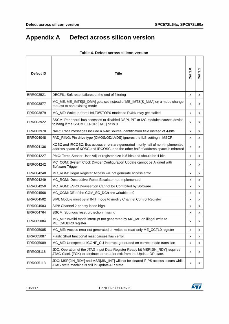
Defect across silicon version SPC572L64x, SPC572L60x
106/117 DocID026771 Rev 2
Appendix A Defect across silicon version
Table 4. Defect across silicon version
Defect ID Title
Cu
t 1
.0
Cu
t 1
.1
ERR003521 DECFIL: Soft reset failures at the end of filtering x x
ERR003877MC_ME: ME_IMTS[S_DMA] gets set instead of ME_IMTS[S_NMA] on a mode change request to non existing mode
x x
ERR003879 MC_ME: Wakeup from HALT0/STOP0 modes to RUNx may get stalled x x
ERR003922SSCM: Peripheral bus accesses to disabled DSPI, PIT or I2C modules causes device to hang if the SSCM EEROR [RAE] bit is 0
x x
ERR003970 NAR: Trace messages include a 6-bit Source Identification field instead of 4-bits x x
ERR004048 PAD_RING: Pin drive type (CMOS/OD/LVDS) ignores the ILS setting in MSCR. x x
ERR004136XOSC and IRCOSC: Bus access errors are generated in only half of non-implemented address space of XOSC and IRCOSC, and the other half of address space is mirrored
x x
ERR004227 PMC: Temp Sensor User Adjust register size is 5 bits and should be 4 bits. x x
ERR004242MC_CGM: System Clock Divider Configuration Update cannot be Aligned with Software Trigger
x x
ERR004248 MC_RGM: Illegal Register Access will not generate access error x x
ERR004249 MC_RGM: 'Destructive' Reset Escalator not Implemented x x
ERR004250 MC_RGM: ESR0 Deassertion Cannot be Controlled by Software x x
ERR004568 MC_CGM: DE of the CGM_SC_DCn are writable to 0 x x
ERR004582 SIPI: Module must be in INIT mode to modify Channel Control Register x x
ERR004583 SIPI: Channel 2 priority is too high x x
ERR004764 SSCM: Spurious reset protection missing x x
ERR005084MC_ME: Invalid mode interrupt not generated by MC_ME on illegal write to ME_CADDR0 register
x x
ERR005085 MC_ME: Access error not generated on writes to read-only ME_CCTL0 register x x
ERR005087 Flash: Short functional reset causes flash error x x
ERR005089 MC_ME: Unexpected ICONF_CU interrupt generated on correct mode transition x x
ERR005116JDC: Operation of the JTAG Input Data Register Ready bit MSR[JIN_RDY] requires JTAG Clock (TCK) to continue to run after exit from the Update-DR state.
x x
ERR005118JDC: MSR[JIN_RDY] and MSR[JIN_INT] will not be cleared if IPS access occurs while JTAG state machine is still in Update-DR state.
x x
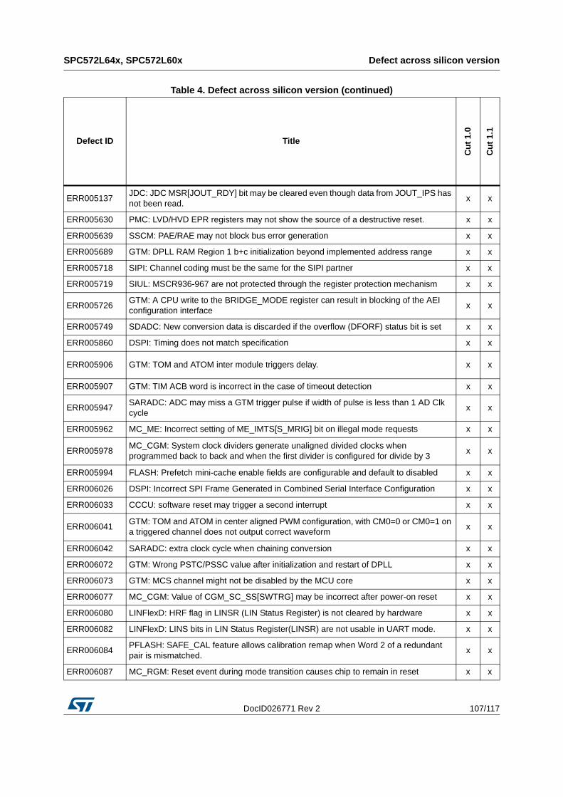
DocID026771 Rev 2 107/117
SPC572L64x, SPC572L60x Defect across silicon version
116
ERR005137JDC: JDC MSR[JOUT_RDY] bit may be cleared even though data from JOUT_IPS has not been read.
x x
ERR005630 PMC: LVD/HVD EPR registers may not show the source of a destructive reset. x x
ERR005639 SSCM: PAE/RAE may not block bus error generation x x
ERR005689 GTM: DPLL RAM Region 1 b+c initialization beyond implemented address range x x
ERR005718 SIPI: Channel coding must be the same for the SIPI partner x x
ERR005719 SIUL: MSCR936-967 are not protected through the register protection mechanism x x
ERR005726GTM: A CPU write to the BRIDGE_MODE register can result in blocking of the AEI configuration interface
x x
ERR005749 SDADC: New conversion data is discarded if the overflow (DFORF) status bit is set x x
ERR005860 DSPI: Timing does not match specification x x
ERR005906 GTM: TOM and ATOM inter module triggers delay. x x
ERR005907 GTM: TIM ACB word is incorrect in the case of timeout detection x x
ERR005947SARADC: ADC may miss a GTM trigger pulse if width of pulse is less than 1 AD Clk cycle
x x
ERR005962 MC_ME: Incorrect setting of ME_IMTS[S_MRIG] bit on illegal mode requests x x
ERR005978MC_CGM: System clock dividers generate unaligned divided clocks when programmed back to back and when the first divider is configured for divide by 3
x x
ERR005994 FLASH: Prefetch mini-cache enable fields are configurable and default to disabled x x
ERR006026 DSPI: Incorrect SPI Frame Generated in Combined Serial Interface Configuration x x
ERR006033 CCCU: software reset may trigger a second interrupt x x
ERR006041GTM: TOM and ATOM in center aligned PWM configuration, with CM0=0 or CM0=1 on a triggered channel does not output correct waveform
x x
ERR006042 SARADC: extra clock cycle when chaining conversion x x
ERR006072 GTM: Wrong PSTC/PSSC value after initialization and restart of DPLL x x
ERR006073 GTM: MCS channel might not be disabled by the MCU core x x
ERR006077 MC_CGM: Value of CGM_SC_SS[SWTRG] may be incorrect after power-on reset x x
ERR006080 LINFlexD: HRF flag in LINSR (LIN Status Register) is not cleared by hardware x x
ERR006082 LINFlexD: LINS bits in LIN Status Register(LINSR) are not usable in UART mode. x x
ERR006084PFLASH: SAFE_CAL feature allows calibration remap when Word 2 of a redundant pair is mismatched.
x x
ERR006087 MC_RGM: Reset event during mode transition causes chip to remain in reset x x
Table 4. Defect across silicon version (continued)
Defect ID Title
Cu
t 1
.0
Cu
t 1
.1
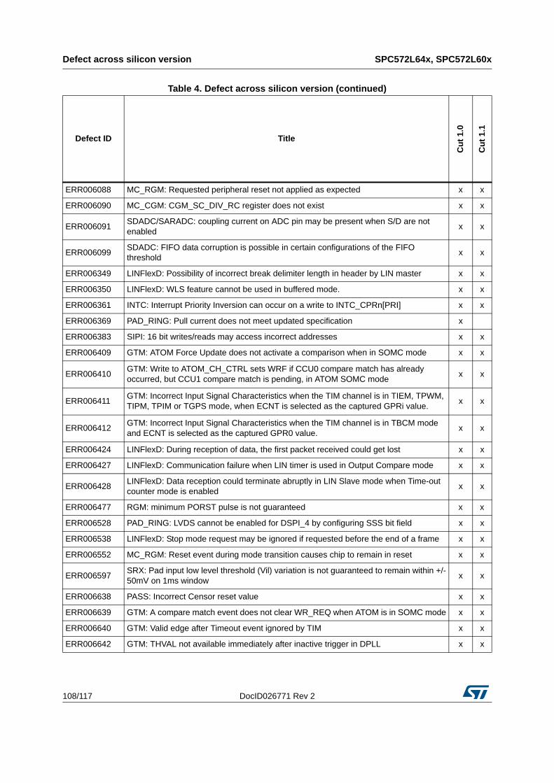
Defect across silicon version SPC572L64x, SPC572L60x
108/117 DocID026771 Rev 2
ERR006088 MC_RGM: Requested peripheral reset not applied as expected x x
ERR006090 MC_CGM: CGM_SC_DIV_RC register does not exist x x
ERR006091SDADC/SARADC: coupling current on ADC pin may be present when S/D are not enabled
x x
ERR006099SDADC: FIFO data corruption is possible in certain configurations of the FIFO threshold
x x
ERR006349 LINFlexD: Possibility of incorrect break delimiter length in header by LIN master x x
ERR006350 LINFlexD: WLS feature cannot be used in buffered mode. x x
ERR006361 INTC: Interrupt Priority Inversion can occur on a write to INTC_CPRn[PRI] x x
ERR006369 PAD_RING: Pull current does not meet updated specification x
ERR006383 SIPI: 16 bit writes/reads may access incorrect addresses x x
ERR006409 GTM: ATOM Force Update does not activate a comparison when in SOMC mode x x
ERR006410GTM: Write to ATOM_CH_CTRL sets WRF if CCU0 compare match has already occurred, but CCU1 compare match is pending, in ATOM SOMC mode
x x
ERR006411GTM: Incorrect Input Signal Characteristics when the TIM channel is in TIEM, TPWM, TIPM, TPIM or TGPS mode, when ECNT is selected as the captured GPRi value.
x x
ERR006412GTM: Incorrect Input Signal Characteristics when the TIM channel is in TBCM mode and ECNT is selected as the captured GPR0 value.
x x
ERR006424 LINFlexD: During reception of data, the first packet received could get lost x x
ERR006427 LINFlexD: Communication failure when LIN timer is used in Output Compare mode x x
ERR006428LINFlexD: Data reception could terminate abruptly in LIN Slave mode when Time-out counter mode is enabled
x x
ERR006477 RGM: minimum PORST pulse is not guaranteed x x
ERR006528 PAD_RING: LVDS cannot be enabled for DSPI_4 by configuring SSS bit field x x
ERR006538 LINFlexD: Stop mode request may be ignored if requested before the end of a frame x x
ERR006552 MC_RGM: Reset event during mode transition causes chip to remain in reset x x
ERR006597SRX: Pad input low level threshold (Vil) variation is not guaranteed to remain within +/-50mV on 1ms window
x x
ERR006638 PASS: Incorrect Censor reset value x x
ERR006639 GTM: A compare match event does not clear WR_REQ when ATOM is in SOMC mode x x
ERR006640 GTM: Valid edge after Timeout event ignored by TIM x x
ERR006642 GTM: THVAL not available immediately after inactive trigger in DPLL x x
Table 4. Defect across silicon version (continued)
Defect ID Title
Cu
t 1
.0
Cu
t 1
.1
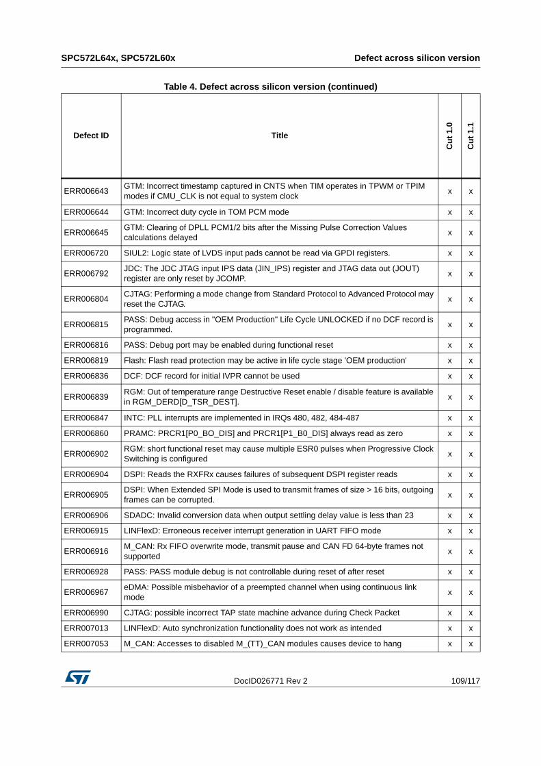
DocID026771 Rev 2 109/117
SPC572L64x, SPC572L60x Defect across silicon version
116
ERR006643GTM: Incorrect timestamp captured in CNTS when TIM operates in TPWM or TPIM modes if CMU_CLK is not equal to system clock
x x
ERR006644 GTM: Incorrect duty cycle in TOM PCM mode x x
ERR006645GTM: Clearing of DPLL PCM1/2 bits after the Missing Pulse Correction Values calculations delayed
x x
ERR006720 SIUL2: Logic state of LVDS input pads cannot be read via GPDI registers. x x
ERR006792JDC: The JDC JTAG input IPS data (JIN_IPS) register and JTAG data out (JOUT) register are only reset by JCOMP.
x x
ERR006804CJTAG: Performing a mode change from Standard Protocol to Advanced Protocol may reset the CJTAG.
x x
ERR006815PASS: Debug access in "OEM Production" Life Cycle UNLOCKED if no DCF record is programmed.
x x
ERR006816 PASS: Debug port may be enabled during functional reset x x
ERR006819 Flash: Flash read protection may be active in life cycle stage 'OEM production' x x
ERR006836 DCF: DCF record for initial IVPR cannot be used x x
ERR006839RGM: Out of temperature range Destructive Reset enable / disable feature is available in RGM_DERD[D_TSR_DEST].
x x
ERR006847 INTC: PLL interrupts are implemented in IRQs 480, 482, 484-487 x x
ERR006860 PRAMC: PRCR1[P0_BO_DIS] and PRCR1[P1_B0_DIS] always read as zero x x
ERR006902RGM: short functional reset may cause multiple ESR0 pulses when Progressive Clock Switching is configured
x x
ERR006904 DSPI: Reads the RXFRx causes failures of subsequent DSPI register reads x x
ERR006905DSPI: When Extended SPI Mode is used to transmit frames of size > 16 bits, outgoing frames can be corrupted.
x x
ERR006906 SDADC: Invalid conversion data when output settling delay value is less than 23 x x
ERR006915 LINFlexD: Erroneous receiver interrupt generation in UART FIFO mode x x
ERR006916M_CAN: Rx FIFO overwrite mode, transmit pause and CAN FD 64-byte frames not supported
x x
ERR006928 PASS: PASS module debug is not controllable during reset of after reset x x
ERR006967eDMA: Possible misbehavior of a preempted channel when using continuous link mode
x x
ERR006990 CJTAG: possible incorrect TAP state machine advance during Check Packet x x
ERR007013 LINFlexD: Auto synchronization functionality does not work as intended x x
ERR007053 M_CAN: Accesses to disabled M_(TT)_CAN modules causes device to hang x x
Table 4. Defect across silicon version (continued)
Defect ID Title
Cu
t 1
.0
Cu
t 1
.1
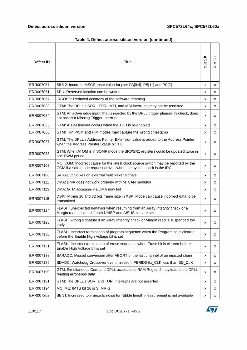
Defect across silicon version SPC572L64x, SPC572L60x
110/117 DocID026771 Rev 2
ERR007057 SIUL2: Incorrect MSCR reset value for pins PA[9:4], PB[11] and PC[2] x x
ERR007061 SPU: Reserved location can be written x x
ERR007067 IRCOSC: Reduced accuracy of the software trimming x x
ERR007083 GTM: The DPLL's SORI, TORI, MTI, and MSI interrupts may not be asserted x x
ERR007084GTM: An active edge input, that is rejected by the DPLL trigger plausibility check, does not assert a Missing Trigger Interrupt
x x
ERR007085 GTM: A TIM timeout occurs when the TDU is re-enabled x x
ERR007086 GTM: TIM PWM and PIM modes may capture the wrong timestamp x x
ERR007087GTM: The DPLL's Address Pointer Extension value is added to the Address Pointer when the Address Pointer Status bit is 0
x x
ERR007088GTM: When ATOM is in SOMP mode the SR0/SR1 registers could be updated twice in one PWM period
x x
ERR007103MC_CGM: Incorrect cause for the latest clock source switch may be reported by the CGM if a safe mode request arrives when the system clock is the IRC
x x
ERR007108 SARADC: Spikes on external multiplexer signals x x
ERR007111 DMA: DMA does not work properly with M_CAN modules x x
ERR007113 DMA: GTM accesses via DMA may fail x x
ERR007115DSPI: Mixing 16 and 32 bits frame size in XSPI Mode can cause incorrect data to be transmitted
x x
ERR007124FLASH: unexpected behavior when resuming from an Array Integrity check or a Margin read suspend if both NAIBP and AISUS bits are set
x x
ERR007125FLASH: wrong signature if an Array Integrity check or Margin read is suspended too early
x x
ERR007130FLASH: Incorrect termination of program sequence when the Program bit is cleared before the Enable High Voltage bit is set
x x
ERR007131FLASH: Incorrect termination of erase sequence when Erase bit is cleared before Enable High Voltage bit is set
x x
ERR007138 SARADC: Missed conversion after ABORT of the last channel of an injected chain x x
ERR007185 SDADC: Watchdog Crossover event missed if PBRIDGEx_CLK less than SD_CLK x x
ERR007190GTM: Simultaneous Core and DPLL accesses to RAM Region 2 may lead to the DPLL reading erroneous data
x x
ERR007191 GTM: The DPLL's SORI and TORI interrupts are not asserted x x
ERR007194 MC_ME: IMTS bit 26 is S_MRIG x x
ERR007202 SENT: Increased tolerance to noise for Nibble length measurement is not available x x
Table 4. Defect across silicon version (continued)
Defect ID Title
Cu
t 1
.0
Cu
t 1
.1
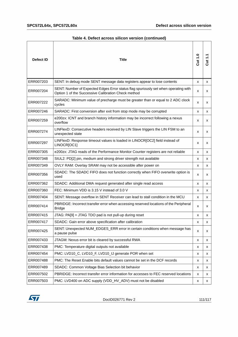
DocID026771 Rev 2 111/117
SPC572L64x, SPC572L60x Defect across silicon version
116
ERR007203 SENT: In debug mode SENT message data registers appear to lose contents x x
ERR007204SENT: Number of Expected Edges Error status flag spuriously set when operating with Option 1 of the Successive Calibration Check method
x x
ERR007222SARADC: Minimum value of precharge must be greater than or equal to 2 ADC clock cycles
x x
ERR007246 SARADC: First conversion after exit from stop mode may be corrupted x x
ERR007259e200zx: ICNT and branch history information may be incorrect following a nexus overflow
x x
ERR007274LINFlexD: Consecutive headers received by LIN Slave triggers the LIN FSM to an unexpected state
x x
ERR007297LINFlexD: Response timeout values is loaded in LINOCR[OC2] field instead of LINOCR[OC1]
x x
ERR007305 e200zx: JTAG reads of the Performance Monitor Counter registers are not reliable x x
ERR007348 SIUL2: PD[2] pin, medium and strong driver strength not available x x
ERR007349 OVLY RAM: Overlay SRAM may not be accessible after power on x x
ERR007356SDADC: The SDADC FIFO does not function correctly when FIFO overwrite option is used
x x
ERR007362 SDADC: Additional DMA request generated after single read access x x
ERR007360 FEC: Minimum VDD is 3.15 V instead of 3.0 V x x
ERR007404 SENT: Message overflow in SENT Receiver can lead to stall condition in the MCU x x
ERR007414PBRIDGE: Incorrect transfer error when accessing reserved locations of the Peripheral Bridge
x x
ERR007415 JTAG: PA[9] = JTAG TDO pad is not pull-up during reset x x
ERR007417 SDADC: Gain error above specification after calibration x x
ERR007425SENT: Unexpected NUM_EDGES_ERR error in certain conditions when message has a pause pulse
x x
ERR007433 JTAGM: Nexus error bit is cleared by successful RWA x x
ERR007438 PMC: Temperature digital outputs not available x x
ERR007454 PMC: LVD10_C, LVD10_F, LVD10_IJ generate POR when set x x
ERR007488 PMC: The Reset Enable bits default values cannot be set in the DCF records x x
ERR007489 SDADC: Common Voltage Bias Selection bit behavior x x
ERR007502 PBRIDGE: Incorrect transfer error information for accesses to FEC reserved locations x x
ERR007503 PMC: LVD400 on ADC supply (VDD_HV_ADV) must not be disabled x x
Table 4. Defect across silicon version (continued)
Defect ID Title
Cu
t 1
.0
Cu
t 1
.1
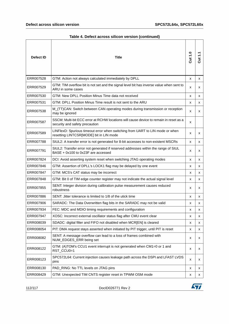
Defect across silicon version SPC572L64x, SPC572L60x
112/117 DocID026771 Rev 2
ERR007528 GTM: Action not always calculated immediately by DPLL x x
ERR007529GTM: TIM overflow bit is not set and the signal level bit has inverse value when sent to ARU in some cases
x x
ERR007530 GTM: New DPLL Position Minus Time data not received x x
ERR007531 GTM: DPLL Position Minus Time result is not sent to the ARU x x
ERR007538M_(TT)CAN: Switch between CAN operating modes during transmission or reception may be ignored
x x
ERR007587SSCM: Multi-bit ECC error at RCHW locations will cause device to remain in reset as a security and safety precaution
x
ERR007589LINFlexD: Spurious timeout error when switching from UART to LIN mode or when resetting LINTCSR[MODE] bit in LIN mode
x x
ERR007788 SIUL2: A transfer error is not generated for 8-bit accesses to non-existent MSCRs x x
ERR007791SIUL2: Transfer error not generated if reserved addresses within the range of SIUL BASE + 0x100 to 0x23F are accessed
x x
ERR007824 DCI: Avoid asserting system reset when switching JTAG operating modes x x
ERR007846 GTM: Assertion of DPLL's LOCK1 flag may be delayed by one event x x
ERR007847 GTM: MCS's CAT status may be incorrect x x
ERR007848 GTM: Bit 0 of TIM edge counter register may not indicate the actual signal level x x
ERR007855SENT: Integer division during calibration pulse measurement causes reduced robustness
x x
ERR007886 SENT: Jitter tolerance is limited to 1/8 of the utick time x x
ERR007906 SARADC: The Data Overwritten flag bits in the SARADC may not be valid x x
ERR007934 FEC: MDC and MDIO timing requirements and configuration x x
ERR007947 XOSC: Incorrect external oscillator status flag after CMU event clear x x
ERR008039 SDADC: digital filter and FIFO not disabled when MCR[EN] is cleared x x
ERR008054 PIT: DMA request stays asserted when initiated by PIT trigger, until PIT is reset x x
ERR008082SENT: A message overflow can lead to a loss of frames combined with NUM_EDGES_ERR being set
x x
ERR008122GTM: (A)TOM's CCU1 event interrupt is not generated when CM1=0 or 1 and RST_CCU0=1
x x
ERR008123SPC572L64: Current injection causes leakage path across the DSPI and LFAST LVDS pins
x x
ERR008130 PAD_RING: No TTL levels on JTAG pins x x
ERR008429 GTM: Unexpected TIM CNTS register reset in TPWM OSM mode x x
Table 4. Defect across silicon version (continued)
Defect ID Title
Cu
t 1
.0
Cu
t 1
.1
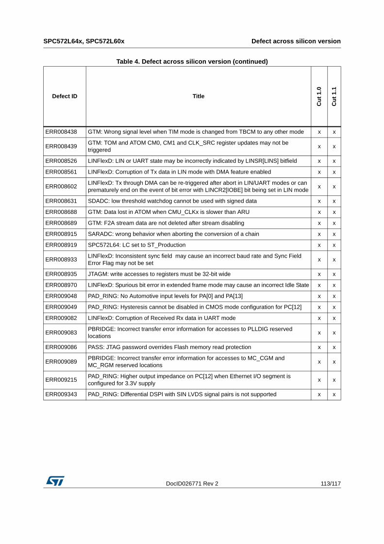
DocID026771 Rev 2 113/117
SPC572L64x, SPC572L60x Defect across silicon version
116
ERR008438 GTM: Wrong signal level when TIM mode is changed from TBCM to any other mode x x
ERR008439GTM: TOM and ATOM CM0, CM1 and CLK_SRC register updates may not be triggered
x x
ERR008526 LINFlexD: LIN or UART state may be incorrectly indicated by LINSR[LINS] bitfield x x
ERR008561 LINFlexD: Corruption of Tx data in LIN mode with DMA feature enabled x x
ERR008602LINFlexD: Tx through DMA can be re-triggered after abort in LIN/UART modes or can prematurely end on the event of bit error with LINCR2[IOBE] bit being set in LIN mode
x x
ERR008631 SDADC: low threshold watchdog cannot be used with signed data x x
ERR008688 GTM: Data lost in ATOM when CMU_CLKx is slower than ARU x x
ERR008689 GTM: F2A stream data are not deleted after stream disabling x x
ERR008915 SARADC: wrong behavior when aborting the conversion of a chain x x
ERR008919 SPC572L64: LC set to ST_Production x x
ERR008933LINFlexD: Inconsistent sync field may cause an incorrect baud rate and Sync Field Error Flag may not be set
x x
ERR008935 JTAGM: write accesses to registers must be 32-bit wide x x
ERR008970 LINFlexD: Spurious bit error in extended frame mode may cause an incorrect Idle State x x
ERR009048 PAD_RING: No Automotive input levels for PA[0] and PA[13] x x
ERR009049 PAD_RING: Hysteresis cannot be disabled in CMOS mode configuration for PC[12] x x
ERR009082 LINFlexD: Corruption of Received Rx data in UART mode x x
ERR009083PBRIDGE: Incorrect transfer error information for accesses to PLLDIG reserved locations
x x
ERR009086 PASS: JTAG password overrides Flash memory read protection x x
ERR009089PBRIDGE: Incorrect transfer error information for accesses to MC_CGM and MC_RGM reserved locations
x x
ERR009215PAD_RING: Higher output impedance on PC[12] when Ethernet I/O segment is configured for 3.3V supply
x x
ERR009343 PAD_RING: Differential DSPI with SIN LVDS signal pairs is not supported x x
Table 4. Defect across silicon version (continued)
Defect ID Title
Cu
t 1
.0
Cu
t 1
.1
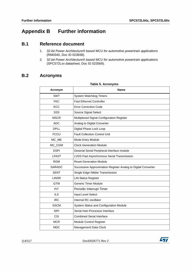
Further information SPC572L64x, SPC572L60x
114/117 DocID026771 Rev 2
Appendix B Further information
B.1 Reference document
1. 32-bit Power Architecture® based MCU for automotive powertrain applications (RM0340, Doc ID 023838).
2. 32-bit Power Architecture® based MCU for automotive powertrain applications (SPC572Lxx datasheet, Doc ID 023569).
B.2 Acronyms
Table 5. Acronyms
Acronym Name
SWT System Watchdog Timers
FEC Fast Ethernet Controller
ECC Error Correction Code
SSS Source Signal Select
MSCR Multiplexed Signal Configuration Register
ADC Analog to Digital Converter
DPLL Digital Phase Lock Loop
FCCU Fault Collection Control Unit
MC_ME Mode Entry Module
MC_CGM Clock Generation Module
DSPI Deserial Serial Peripheral Interface module
LFAST LVDS Fast Asynchronous Serial Transmission
RGM Reset Generation Module
SARADC Successive Approximation Register Analog to Digital Converter
SENT Single Edge Nibble Transmission
LINSR LIN Status Register
GTM Generic Timer Module
PIT Periodic Interrupt Timer
ILS Input Level Select
IRC Internal RC oscillator
SSCM System Status and Configuration Module
SIPI Serial Inter-Processor Interface
CSI Combined Serial Interface
MCR Module Control Register
MDC Management Data Clock
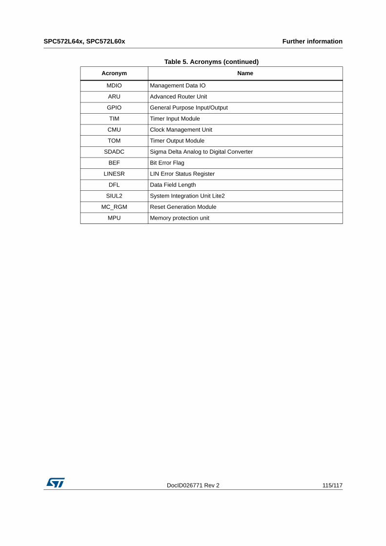
DocID026771 Rev 2 115/117
SPC572L64x, SPC572L60x Further information
116
MDIO Management Data IO
ARU Advanced Router Unit
GPIO General Purpose Input/Output
TIM Timer Input Module
CMU Clock Management Unit
TOM Timer Output Module
SDADC Sigma Delta Analog to Digital Converter
BEF Bit Error Flag
LINESR LIN Error Status Register
DFL Data Field Length
SIUL2 System Integration Unit Lite2
MC_RGM Reset Generation Module
MPU Memory protection unit
Table 5. Acronyms (continued)
Acronym Name
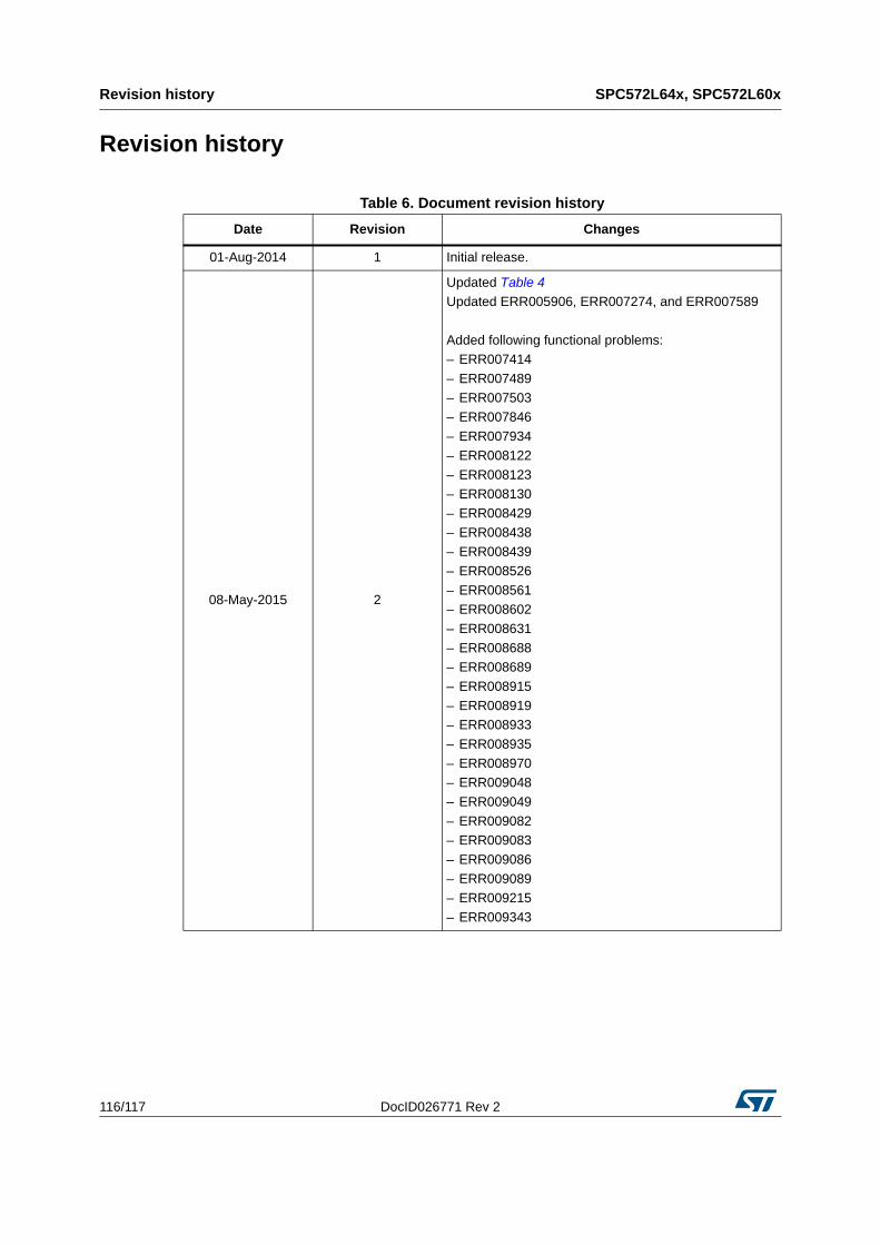
Revision history SPC572L64x, SPC572L60x
116/117 DocID026771 Rev 2
Revision history
Table 6. Document revision history
Date Revision Changes
01-Aug-2014 1 Initial release.
08-May-2015 2
Updated Table 4
Updated ERR005906, ERR007274, and ERR007589
Added following functional problems:
– ERR007414
– ERR007489
– ERR007503
– ERR007846
– ERR007934
– ERR008122
– ERR008123
– ERR008130
– ERR008429
– ERR008438
– ERR008439
– ERR008526
– ERR008561
– ERR008602
– ERR008631
– ERR008688
– ERR008689
– ERR008915
– ERR008919
– ERR008933
– ERR008935
– ERR008970
– ERR009048
– ERR009049
– ERR009082
– ERR009083
– ERR009086
– ERR009089
– ERR009215
– ERR009343
DocID026771 Rev 2 117/117
SPC572L64x, SPC572L60x
117
IMPORTANT NOTICE – PLEASE READ CAREFULLY
STMicroelectronics NV and its subsidiaries (“ST”) reserve the right to make changes, corrections, enhancements, modifications, and improvements to ST products and/or to this document at any time without notice. Purchasers should obtain the latest relevant information on ST products before placing orders. ST products are sold pursuant to ST’s terms and conditions of sale in place at the time of order acknowledgement.
Purchasers are solely responsible for the choice, selection, and use of ST products and ST assumes no liability for application assistance or the design of Purchasers’ products.
No license, express or implied, to any intellectual property right is granted by ST herein.
Resale of ST products with provisions different from the information set forth herein shall void any warranty granted by ST for such product.
ST and the ST logo are trademarks of ST. All other product or service names are the property of their respective owners.
Information in this document supersedes and replaces information previously supplied in any prior versions of this document.
© 2015 STMicroelectronics – All rights reserved