Embed Size (px)
Citation preview

September 2013 Doc ID 18380 Rev 4 1/29
SPC560P40/SPC560P34Errata sheet
SPC560P40/SPC560P34 device errataJTAG_ID = 0x1AE2_2041
IntroductionThis errata sheet describes all the functional and electrical problems of the SPC560P40/SPC560P34 devices, identified with the JTAG_ID = 0x1AE2_2041.
All the topics covered in this document refer to RM0046 rev 2 and SPC560P34L1, SPC560P34L3, SPC560P40L1, SPC560P40L3 datasheet rev 3 (see Appendix B: Further information).
Device identification for cut 1.1:
■ JTAG_ID = 0x1AE2_2041
■ MIDR1 register:– MAJOR_MASK[3:0]: 4’b0000– MINOR_MASK[3:0]: 4’b0001
Package device marking mask identifier: AB
Die mask ID: FP40X1
This errata sheet applies to SPC560P40/SPC560P34 devices in accordance with Table 1.
Table 1. Device summary
Part number Package
SPC560P34L1 LQFP64
SPC560P34L3 LQFP100
SPC560P40L1 LQFP64
SPC560P40L3 LQFP100
www.st.com

SPC560P40/SPC560P34 Contents
Doc ID 18380 Rev 4 2/29
Contents
1 Functional problems . . . . . . . . . . . . . . . . . . . . . . . . . . . . . . . . . . . . . . . . . 6
1.1 ERR000575: DSPI: Changing CTARs between frames in continuous PCS mode causes error . . . . . . . . . . . . . . . . . . . . . . . . . . . . . . . . . . . . . . . . . . . 6
1.2 ERR001082: DSPI: set up enough ASC time when MTFE = 1 and CPHA = 1 . . . . . . . . . . . . . . . . . . . . . . . . . . . . . . . . . . . . . . . . . . . . . . . . . . . . . . . . . . 6
1.3 ERR001103: DSPI: PCS continuous selection format limitation . . . . . . . . 6
1.4 ERR002360: FlexCAN: Global masks misalignment . . . . . . . . . . . . . . . . . 7
1.5 ERR002656: FlexCAN: Abort request blocks the CODE field . . . . . . . . . . 8
1.6 ERR002685: FlexCAN: Module disable mode functionality not described correctly . . . . . . . . . . . . . . . . . . . . . . . . . . . . . . . . . . . . . . . . . . . . . . . . . . . 8
1.7 ERR002883: FMPLL: FMPLL_CR[UNLOCK_ONCE] wrongly set . . . . . . . 9
1.8 ERR002894: ADC: Minimum sampling time for ADC at 32 MHz . . . . . . . . 9
1.9 ERR002897: ADC: Offset cancellation not required . . . . . . . . . . . . . . . . . 9
1.10 ERR002958: MC_RGM: Clearing a flag at RGM_DES or RGM_FES register may be prevented by a reset . . . . . . . . . . . . . . . . . . . . . . . . . . . . . . . . . . . 9
1.11 ERR002963: CMU XOSC Monitoring cannot be guaranteed when RCDIV > 0 and FOSC is less than 1.5 * Frc/2RCDIV . . . . . . . . . . . . . . . . . 10
1.12 ERR002971: ADC ABORT bit (single conversion) . . . . . . . . . . . . . . . . . . 10
1.13 ERR002972: ADC: Last conversion in chain not aborted . . . . . . . . . . . . 10
1.14 ERR002973: ADC ABORT CHAIN bit . . . . . . . . . . . . . . . . . . . . . . . . . . . 10
1.15 ERR002981: FMPLL: Do not poll flag FMPLL_CR[PLL_FAIL] . . . . . . . . . .11
1.16 ERR002997: ADC: Injected conversion not executed during scan mode. .11
1.17 ERR002999: MC_CGM and MC_PCU: A data storage exception is not generated on an access to MC_CGM or MC_PCU when the respective peripheral is disabled at MC_ME. . . . . . . . . . . . . . . . . . . . . . . . . . . . . . . .11
1.18 ERR003010: ADC: conversion chain failing after ABORT chain . . . . . . . .11
1.19 ERR003021: LINFlex: Unexpected LIN timeout in slave mode . . . . . . . . 12
1.20 ERR003028: LINFlex: BDRL/BDRM cannot be accessed as byte or half-word . . . . . . . . . . . . . . . . . . . . . . . . . . . . . . . . . . . . . . . . . . . . . . . . . . 12
1.21 ERR003060: MC_RGM: SAFE mode exit may be possible even though condition causing the SAFE mode request has not been cleared . . . . . . 12
1.22 ERR003069: ADC: ADC_DMAE[DCLR] set to 1 clears the DMA request incorrectly . . . . . . . . . . . . . . . . . . . . . . . . . . . . . . . . . . . . . . . . . . . . . . . . . 13
SPC560P40/SPC560P34 Contents
Doc ID 18380 Rev 4 3/29
1.23 ERR003110: Debugging functionality could be lost when unsecuring a secured device. . . . . . . . . . . . . . . . . . . . . . . . . . . . . . . . . . . . . . . . . . . . . 13
1.24 ERR003164: FCU: Timeout feature does not work correctly. . . . . . . . . . . 13
1.25 ERR003220: MC_CGM: system clock may stop in case target clock source dies during clock switching. . . . . . . . . . . . . . . . . . . . . . . . . . . . . . . . . . . . 14
1.26 ERR003248: ADC:Abort request during last sampling cycle corrupts the data register of next channel conversion . . . . . . . . . . . . . . . . . . . . . . . . . 14
1.27 ERR003256: eTimer: Configuring an eTimer counter channel in GATED-COUNT mode or in SIGNED-COUNT mode may cause a possible incorrect counting of 1 tick. . . . . . . . . . . . . . . . . . . . . . . . . . . . . . . . . . . . . 14
1.28 ERR003257: FlexPWM: Configuring the count value to set PWMA/PWMB first low and then high in the same cycle the output signals are low. . . . . 15
1.29 ERR003262: Register protection on full CMU_CSR . . . . . . . . . . . . . . . . 15
1.30 ERR003263: Serial boot and censorship: Flash read access . . . . . . . . . 16
1.31 ERR003264: MCM: MRSR does not report power on reset event . . . . . . 16
1.32 ERR003269: MC_ME: Peripheral clocks may get incorrectly disabled or enabled after entering debug mode . . . . . . . . . . . . . . . . . . . . . . . . . . . . . 16
1.33 ERR003310: FlexPWM: PWM signals are improperly synced when using master sync . . . . . . . . . . . . . . . . . . . . . . . . . . . . . . . . . . . . . . . . . . . . . . . 17
1.34 ERR003324: FIRC -FIRC_CTL[TRIM] does not display correct trim value after reset . . . . . . . . . . . . . . . . . . . . . . . . . . . . . . . . . . . . . . . . . . . . . . . . . 17
1.35 ERR003335: FlexPWM: Incorrect PWM operation when mixing DMA and non-DMA controlled channels . . . . . . . . . . . . . . . . . . . . . . . . . . . . . . . . . 17
1.36 ERR003377: Pad Ring: Nexus pins may drive an unknown value immediately after power up but before the 1st clock edge . . . . . . . . . . . . 18
1.37 ERR003407: FlexCAN: CAN transmitter stall in case of no remote frame in response to Tx packet with RTR = 1 18
1.38 ERR003442: CMU monitor: FXOSC/FIRC and FMPLL/FIRC relation. . . 19
1.39 ERR003452: FLASH: Programming just after reading a location of Data Flash with double ECC error can trigger a functional reset. . . . . . . . . . . . 19
1.40 ERR003511: FlexPWM : Incorrect PWM operation when IPOL is set. . . 19
1.41 ERR003547: FLASH: Running ECC logic check just after reading a location of data Flash with double ECC error can trigger a functional reset. . . . . . 20
1.42 ERR003583: MC_RGM: A non-monotonic ramp on the VDD_HV_REG supply can cause the RGM module to clear all flags in the DES register. 20
1.43 ERR003584: MC_ME: Possibility of machine check on low-power mode exit . . . . . . . . . . . . . . . . . . . . . . . . . . . . . . . . . . . . . . . . . . . . . . . . . . . . . . . . . 21
SPC560P40/SPC560P34 Contents
Doc ID 18380 Rev 4 4/29
Appendix A Defects across silicon version . . . . . . . . . . . . . . . . . . . . . . . . . . . . . 23
Appendix B Further information . . . . . . . . . . . . . . . . . . . . . . . . . . . . . . . . . . . . . . 25
B.1 Reference document . . . . . . . . . . . . . . . . . . . . . . . . . . . . . . . . . . . . . . . . . 25
B.2 Acronyms . . . . . . . . . . . . . . . . . . . . . . . . . . . . . . . . . . . . . . . . . . . . . . . . . 25
Revision history . . . . . . . . . . . . . . . . . . . . . . . . . . . . . . . . . . . . . . . . . . . . . . . . . . . . 27

SPC560P40/SPC560P34 List of tables
Doc ID 18380 Rev 4 5/29
List of tables
Table 1. Device summary . . . . . . . . . . . . . . . . . . . . . . . . . . . . . . . . . . . . . . . . . . . . . . . . . . . . . . . . . . 1Table 2. Defects across silicon version . . . . . . . . . . . . . . . . . . . . . . . . . . . . . . . . . . . . . . . . . . . . . . 23Table 3. Acronyms . . . . . . . . . . . . . . . . . . . . . . . . . . . . . . . . . . . . . . . . . . . . . . . . . . . . . . . . . . . . . . 25Table 4. Document revision history . . . . . . . . . . . . . . . . . . . . . . . . . . . . . . . . . . . . . . . . . . . . . . . . . 27

SPC560P40/SPC560P34 Functional problems
Doc ID 18380 Rev 4 6/29
1 Functional problems
1.1 ERR000575: DSPI: Changing CTARs between frames in continuous PCS mode causes error
Description:
Erroneous data could be transmitted if multiple Clock and Transfer Attribute Registers (CTAR) are used while using the Continuous Peripheral Chip Select mode (DSPIx_PUSHR[CONT = 1]). The conditions that can generate an error are:
1. If DSPIx_CTARn[CPHA] = 1 and DSPIx_MCR[CONT_SCKE = 0] and DSPIx_CTARn[CPOL, CPHA, PCSSCK or PBR] change between frames.
2. If DSPIx_CTARn[CPHA]=0 or DSPIx_MCR[CONT_SCKE = 1] and any bit field of DSPIx_CTARn changes between frames except DSPIx_CTARn[PBR].
Workaround:
When generating DSPI bit frames in continuous PCS mode, adhere to the aforementioned conditions when changing DSPIx_CTARn bit fields between frames.
1.2 ERR001082: DSPI: set up enough ASC time when MTFE = 1 and CPHA = 1
Description:
When the DSPI is being used in the modified transfer format mode (DSPI_MCR[MTFE]=1) with the clock phase set for data changing on the leading edge of the clock and captured on the following edge in the DSPI clock and transfer attributes register (DSPI_CTARn[CPHA]=1), if the After SCK delay scaler (ASC) time is set to less than 1/2 SCK clock period the DSPI may not complete the transaction, the TCF flag is not set, serial data is not received, and last transmitted bit can be truncated.
Workaround:
If the modified transfer format mode is required DSPI_MCR[MTFE] = 1 with the clock phase set for serial data changing on the leading edge of the clock and captured on the following edge in the SCK clock (Transfer Attributes Register (DSPI_CTARn[CPHA] = 1) make sure that the ASC time is set to be longer than half SCK clock period.
1.3 ERR001103: DSPI: PCS continuous selection format limitation
Description:
When the DSPI module has more than one entry in the TX FIFO and only one entry is written and that entry has the CONT bit set, and continuous SCK clock selected the PCS levels may change between transfer complete and write of the next data to the DSPI_PUSHR register.
For example, if the CONT bit is set with the first PUSHR write, the PCS de-asserts after the transfer because the configuration data for the next frame has already been fetched from
SPC560P40/SPC560P34 Functional problems
Doc ID 18380 Rev 4 7/29
the next (empty) fifo entry. This behavior continues till the buffer is filled once and all CONT bits are one.
To insure PCS stability during data transmission in Continious Selection Format and Continious SCK clock enabled make sure that the data with reset CONT bit is written to DSPI_PUSHR register before previous data sub-frame (with CONT bit set) transfer is over.
Workaround:
No workaround.
1.4 ERR002360: FlexCAN: Global masks misalignment Description:
Convention: MSB = 0.
During CAN messages reception by FlexCAN, the RXGMASK (Rx Global Mask) is used as acceptance mask for most of the Rx message buffers (MB). When the FIFO Enable bit in the FlexCAN module configuration register (CANx_MCR[FEN], bit 2) is set, the RXGMASK also applies to most of the elements of the ID filter table. However there is a misalignment between the position of the ID field in the Rx MB and in RXIDA, RXIDB and RXIDC fields of the ID Tables. In fact RXIDA filter in the ID Tables is shifted one bit to the left from Rx MBs ID position as shown below:
● Rx MB ID = bits 3–31 of ID word corresponding to message ID bits 0–28
● RXIDA = bits 2–30 of ID Table corresponding to message ID bits 0–28
Note that the mask bits one-to-one correspondence occurs with the filters bits, not with the incoming message ID bits. This leads the RXGMASK to affect Rx MB and Rx FIFO filtering in different ways.
For example, if the user intends to mask out the bit 24 of the ID filter of message buffers then the RXGMASK is configured as 0xffff_ffef. As result, bit 24 of the ID field of the incoming message is ignored during filtering process for message buffers. This very same configuration of RXGMASK would lead bit 24 of RXIDA to be “don't care” and thus bit 25 of the ID field of the incoming message would be ignored during filtering process for Rx FIFO.
Similarly, both RXIDB and RXIDC filters have multiple misalignments with regards to position of ID field in Rx MBs, which can lead to erroneous masking during filtering process for either Rx FIFO or MBs.
RX14MASK (Rx 14 Mask) and RX15MASK (Rx 15 Mask) have the same structure as the RXGMASK. This includes the misalignment problem between the position of the ID field in the Rx MBs and in RXIDA, RXIDB and RXIDC fields of the ID Tables.
Workaround:
Therefore it is recommended that one of the following actions be taken to avoid problems:
● Do not enable the RxFIFO. If CANx_MCR[FEN] = 0 then the Rx FIFO is disabled and thus the masks RXGMASK, RX14MASK and RX15MASK do not affect it.
● Enable Rx individual mask registers. If the backwards compatibility configuration bit in the FlexCAN module configuration register (CANx_MCR[BCC], bit 15) is set then the Rx individual mask registers (RXIMR[0:63]) are enabled and thus the masks RXGMASK, RX14MASK and RX15MASK are not used.
● Do not use masks RXGMASK, RX14MASK and RX15MASK (that is, let them in reset value which is 0xffff_ffff) when CANx_MCR[FEN] =1 and CANx_MCR[BCC] = 0. In this

SPC560P40/SPC560P34 Functional problems
Doc ID 18380 Rev 4 8/29
case, filtering processes for both Rx MBs and Rx FIFO are not affected by those masks.
● Do not configure any MB as Rx (that is, let all MBs as either Tx or inactive) when CANx_MCR[FEN] = 1 and CANx_MCR[BCC] = 0. In this case, the masks RXGMASK, RX14MASK and RX15MASK can be used to affect ID tables without affecting filtering process for Rx MBs.
1.5 ERR002656: FlexCAN: Abort request blocks the CODE fieldDescription:
An Abort request to a transmit Message Buffer (TxMB) can block any write operation into its CODE field. Therefore, the TxMB cannot be aborted or deactivated until it completes a valid transmission (by winning the CAN bus arbitration and transmitting the contents of the TxMB).
Workaround:
Instead of aborting the transmission, use deactivation instead.
Note that there is a chance the the deactivated TxMB can be transmitted without setting IFLAG and updating the CODE field if it is deactivated.
1.6 ERR002685: FlexCAN: Module disable mode functionality not described correctly
Description:
Module Disable Mode functionality is described as the FlexCAN block is directly responsible for shutting down the clocks for both CAN Protocol Interface (CPI) and Message Buffer Management (MBM) sub-modules. In fact, FlexCAN requests this action to an external logic.
Workaround:
In FlexCAN documentation chapter:
Section “Modes of Operation”, bullet “Module Disable Mode”: Where is written: “This low power mode is entered when the MDIS bit in the MCR Register is asserted. When disabled, the module shuts down the clocks to the CAN Protocol Interface and Message Buffer Management sub-modules.”.
The correct description is: “This low power mode is entered when the MDIS bit in the MCR Register is asserted by the CPU. When disabled, the module requests to disable the clocks to the CAN Protocol Interface and Message Buffer Management sub-modules.”
Section “Modes of Operation Details”, Sub-section “Module Disable Mode”: Where is written: “This low power mode is entered when the MDIS bit in the MCR Register is asserted. If the module is disabled during Freeze Mode, it shuts down the clocks to the CPI and MBM sub-modules, sets the LPM_ACK bit and negates the FRZ_ACK bit.”.
The correct description is: “This low power mode is entered when the MDIS bit in the MCR Register is asserted. If the module is disabled during Freeze Mode, it requests to disable the clocks to the CAN Protocol Interface (CPI) and Message Buffer Management (MBM) sub-modules, sets the LPM_ACK bit and negates the FRZ_ACK bit.”

SPC560P40/SPC560P34 Functional problems
Doc ID 18380 Rev 4 9/29
1.7 ERR002883: FMPLL: FMPLL_CR[UNLOCK_ONCE] wrongly set
Description:
If the FMPLL is locked and a functional reset occurs, FMPLL_CR[UNLOCK_ONCE] is automatically set even when the FMPLL has not lost lock.
Workaround:
Do not use the FMPLL_CR[UNLOCK_ONCE] when a functional reset occurs.
1.8 ERR002894: ADC: Minimum sampling time for ADC at 32 MHz
Description:
When ADC is running at 32 MHz the minimum sampling time of 135ns specified is not met.
Workaround:
At 32 MHZ the minimum sampling time must be at least 180 ns.
1.9 ERR002897: ADC: Offset cancellation not requiredDescription:
The offset cancellation mechanism does not improve the ADC performance as the intrinsic ADC precision is better than the offset cancellation resolution.
Workaround:
Do not use the offset cancellation feature as it does not improve ADC precision.
1.10 ERR002958: MC_RGM: Clearing a flag at RGM_DES or RGM_FES register may be prevented by a reset
Description:
Clearing a flag at RGM_DES and RGM_FES registers requires two clock cycles because of a synchronization mechanism. As a consequence if a reset occurs while clearing is on-going the reset may interrupt the clearing mechanism leaving the flag set.
Note that this failed clearing has no impact on further flag clearing requests.
Workaround:
No workaround for all reset sources except SW reset.
Note that in case the application requests a SW reset immediately after clearing a flag in RGM_xES the same issue may occur. To avoid this effect the application must ensure that flag clearing has completed by reading the RGM_xES register before the SW reset is requested.

SPC560P40/SPC560P34 Functional problems
Doc ID 18380 Rev 4 10/29
1.11 ERR002963: CMU XOSC Monitoring cannot be guaranteed when RCDIV > 0 and FOSC is less than 1.5 * Frc/2RCDIV
Description:
A false OLRI (Oscillator frequency less than RC frequency) event may be generated when FOSC is less than 1.5 * (FRC / 2RCDIV) and RCDIV > 0, and not FRC / 2RCDIV as described in RM0022 (see B.1: Reference document in Appendix B). Correct crystal clock monitoring is guaranteed when FOSC is strictly above 1.5 * (FRC / 2RCDIV).
Workaround:
There are 2 workarounds available :
1. Keep RCDIV = 0
2. When RCDIV > 0, ensure FOSC is greater than FRC / 2(RCDIV – 1) to avoid false OLRI (CMU external oscillator failure) event.
1.12 ERR002971: ADC ABORT bit (single conversion) Description:
If user starts one single ADC conversion and, immediately afterwards starts a chain of conversions, when he tries to abort one of these conversions, the ABORT command suspends the execution of all conversions instead of a single one.
Workaround:
There are 2 workarounds available:
● At least two conversions has to be programmed.
● A dummy conversion must be started before or after a single conversion.
1.13 ERR002972: ADC: Last conversion in chain not aborted Description:
If the user aborts the last ADC conversion of a chain of conversions, this conversion appears to be aborted, but the relevant data register is anyway updated with the conversion data.
Workaround:
No workaround
1.14 ERR002973: ADC ABORT CHAIN bit Description:
If user aborts a chain of ADC conversions, the current conversion appears as aborted but the relative data register is however updated.
Workaround:
No workaround

SPC560P40/SPC560P34 Functional problems
Doc ID 18380 Rev 4 11/29
1.15 ERR002981: FMPLL: Do not poll flag FMPLL_CR[PLL_FAIL] Description:
For the case when the FMPLL is indicating loss of lock the flag FMPLL_CR[PLL_FAIL] is unpredictable.
Workaround:
To avoid reading an incorrect value of FMPLL_CR[PLL_FAIL] only read this flag inside the FMPLL Interrupt Service Routine (ISR). The ISR indicates the flag has been set correctly and at this point the flag can be cleared. Do not poll flag FMPLL_CR[PLL_FAIL] at any other point in the application software.
1.16 ERR002997: ADC: Injected conversion not executed during scan mode.
Description:
When ADC is converting a chain in scan mode, configured using NSTART bit in non-CTU mode operation and a injected conversion arrives, triggered by software with JSTART bit or by hardware from eTimer_1 channel 5 (internal connection), the ADC gets stuck in the sampling phase (the triggered conversion is not executed and the chain is not restarted).
Workaround:
No workaround
1.17 ERR002999: MC_CGM and MC_PCU: A data storage exception is not generated on an access to MC_CGM or MC_PCU when the respective peripheral is disabled at MC_ME.
Description:
If a peripheral with registers mapped to MC_CGM or MC_PCU address spaces is disabled via the MC_ME any read or write accesses to this peripheral is ignored without producing a data storage exception.
Workaround:
For any mode other than a low-power mode do not disable any peripheral that is mapped to MC_CGM or MC_PCU.
1.18 ERR003010: ADC: conversion chain failing after ABORT chain
Description:
During a chain of conversions, while the ADC is in scan mode, when ADC_MCR[ABORTCHAIN] is asserted, the current chain is aborted as expected. However, in the next scan the first conversion of the chain is performed twice and the last one is not performed at all.
SPC560P40/SPC560P34 Functional problems
Doc ID 18380 Rev 4 12/29
Workaround:
When aborting a chain conversion enable ADC_MCR[ABORTCHAIN] and disable ADC_MCR[START]. ADC_MCR[START] can be enabled when the abort is complete.
1.19 ERR003021: LINFlex: Unexpected LIN timeout in slave mode Description:
If the LINFlex is configured in LIN slave mode, an unexpected LIN timeout event (LINESR[OCF]) may occur during LIN Break reception.
Workaround:
It is recommended to disable this functionality during LINFlex initialization by clearing LINTCSR[IOT] and LINIER[OCIE] bits, and ignore timeout events.
1.20 ERR003028: LINFlex: BDRL/BDRM cannot be accessed as byte or half-word
Description:
LINFlex data buffers (BDRL/BDRM) cannot be accessed as byte or half word. Accessing BDRL/BDRM in byte/half word mode leads to incorrect data writing/reading.
Workaround:
Access BDRL/BDRM registers as word only.
1.21 ERR003060: MC_RGM: SAFE mode exit may be possible even though condition causing the SAFE mode request has not been cleared
Description:
A SAFE mode exit should not be possible as long as any condition that caused a SAFE mode entry is still active. However, if the corresponding status flag in the RGM_FES register has been cleared, the SAFE mode exit may incorrectly occur even though the actual condition is still active.
Workaround:
Software must clear the SAFE mode request condition at the source before clearing the corresponding RGM_FES flag. This ensures that the condition is no longer active when the RGM_FES flag is cleared and thus the SAFE mode exit can occur under the correct conditions.
SPC560P40/SPC560P34 Functional problems
Doc ID 18380 Rev 4 13/29
1.22 ERR003069: ADC: ADC_DMAE[DCLR] set to 1 clears the DMA request incorrectly
Description:
When ADC_DMAE[DCLR] is set, the DMA request should be cleared only after the data registers are read. However for this case the DMA request is automatically cleared and is not recognised by the eDMA.
Workaround:
No workaround
1.23 ERR003110: Debugging functionality could be lost when unsecuring a secured device.
Description:
Providing the backdoor password via JTAG or via serial boot would unsecure the device, but on some devices may leave the Nexus interface and potentially the CPUs in an undetermined state. Normal operation without a debugger is unaffected, debugging unsecured devices is also unaffected.
Workaround:
There are 4 workarounds available:
● A second connection attempt may be successful.
● Boot in serial mode (using the Flash password), then execute the code which unsecures the device (the JTAG interface needs to be inactive while the unsecure event happens).
● Implement a separate backdoor in application software. Once the software detects the custom backdoor sequence it can unlock the device via Flash write.
● Leave device unsecured for debugging.
1.24 ERR003164: FCU: Timeout feature does not work correctly.Description:
When a fault occurs, a timeout for this fault is enabled and the fault is not recovered automatically before the timeout occurrence: In this case the device goes into ALARM state and waits for a timeout; after the timeout has elapsed it enters FAULT state. However, if another fault occurs with the timeout enabled the FCU goes directly into FAULT state without waiting for the timeout to elapse.
If the FCU should again go into ALARM state for the second fault, a Watchdog reset must be asserted after the first fault is detected.
Workaround:
No workaround

SPC560P40/SPC560P34 Functional problems
Doc ID 18380 Rev 4 14/29
1.25 ERR003220: MC_CGM: system clock may stop in case target clock source dies during clock switching.
Description:
The clock switching is a two step process. The availability of the target clock is first verified. Then the system clock is switched to the new target clock source within two target clock cycles.
For the case when the FXOSC stops during the required two cycles, the switching process may not complete, causing the system clock to stop and prevent further clock switching. This may happen if one of the following cases occurs while the system clock source is switching to FXOSC:
● FXOSC oscillator failure
● SAFE mode request occurs, as this mode immediately switches off the FXOSC (refer to ME_SAFE_MC register configuration)
Workaround:
The device is able to recover through any destructive reset event, so typically either the SWT (internal watchdog) generates a reset and the device restarts properly after reset.
To reduce the probability that this issue occurs in the application, it is recommended to disable SAFE mode transitions when the device is executing a mode transition with the FXOSC as the system clock source in the target mode.
1.26 ERR003248: ADC:Abort request during last sampling cycle corrupts the data register of next channel conversion
Description:
If the abort pulse is valid in the last cycle of the SAMPLE phase, the current channel is correctly aborted but the data register (CDR[0:15]) of the next channel conversion shows an invalid value.
Workaround:
No workaround
1.27 ERR003256: eTimer: Configuring an eTimer counter channel in GATED-COUNT mode or in SIGNED-COUNT mode may cause a possible incorrect counting of 1 tick.
Description:
This bug affects eTimer in the following counting modes:
● GATED-COUNT mode: the CNTMODE field is ‘011’ (count rising edges of primary source while secondary input is high)
● SIGNED-COUNT mode: the CNTMODE field is ‘101’ (count primary source rising edges, secondary source specifies direction (up/down)).
Delays in the edge detection circuitry lead to a bug where the rising edge on the primary source is compared to the secondary source value one clock later in time. This means that if
SPC560P40/SPC560P34 Functional problems
Doc ID 18380 Rev 4 15/29
there is a rising edge on the primary source followed immediately by the secondary source going high, the eTimer logic could see this as a rising primary edge while the secondary is high even though the secondary input was low at the time of the rising primary edge.
This bug can occur when the transition on the secondary edge occurs within 1 IPBus clock cycle of the transition on the primary input.
The counter also increments if the primary source is already high when the secondary source goes high.
Workaround:
The source selected as the secondary input to the eTimer channel needs to have an additional clock cycle of delay added to it. This can be done by using the input filters. For the primary source set FILT_PER==1 and FILT_CNT==0. For the secondary source set FILT_PER==1 and FILT_CNT==1. This introduces a 5 clock cycles latency on the primary source and a 6 cycles latency on the secondary source which properly align the two signals for count modes ‘011’ and ‘101’.
Ensure that the primary source is low before the secondary source goes high to avoid a false count caused by the second form of this bug.
1.28 ERR003257: FlexPWM: Configuring the count value to set PWMA/PWMB first low and then high in the same cycle the output signals are low.
Description:
The VAL2 and VAL4 registers define the turn-on edge and the VAL3 and VAL5 registers define the turn off edge of the PWMA/PWMB signals respectively. VAL3 cannot be less than VAL2 and VAL5 cannot be less than VAL4. Doing so causes the PWM signal to turn off at the correct time (VAL3 or VAL5), but it does not turn on at the time defined by VAL2 or VAL4.
This can be an issue during the generation of phase delayed pulses where the PWM signal goes high late in PWM cycle N and remains high across the cycle boundary before going low early in cycle N+1 and goes high again in PWM cycle N+1. This errata allows that to happen.
VAL3 register must be “greater than or equal to” VAL2 register and VAL5 must be “greater than or equal to” VAL4.
Workaround:
No workaround
1.29 ERR003262: Register protection on full CMU_CSRDescription:
The register protection on CMU_CSR of CMU0 works only on the full 32 bit, while it should protect only the bits 24–31. As a consequence, when register protection is active on CMU_CSR the frequency meter cannot be used anymore.

SPC560P40/SPC560P34 Functional problems
Doc ID 18380 Rev 4 16/29
Workaround:
In order to perform a frequency meter operation, the register protection of the relevant CMU must be disabled first; this workaround would work only when soft lock is active.
1.30 ERR003263: Serial boot and censorship: Flash read accessDescription:
In a secured device, starting with a serial boot, it is possible to read the content of the four Flash locations where the RCHW is stored. For example if the RCHW is stored at address 0x00000000, the reads at address 0x00000000, 0x00000004, 0x00000008 and 0x0000000C returns a correct value. Any other flash address is not readable.
Workaround:
No workaround
1.31 ERR003264: MCM: MRSR does not report power on reset event
Description:
The flag POR of MRSR register stays low after power on reset event on the device.
Workaround:
Do not use MRSR[POR] to determine power on reset cause. Use RGM_DES instead.
1.32 ERR003269: MC_ME: Peripheral clocks may get incorrectly disabled or enabled after entering debug mode
Description:
If ME_RUN_PCx, ME_LP_PCx, ME_PCTLx registers are changed to enable or disable a peripheral, and the device enters debug mode before a subsequent mode transition, the peripheral clock gets enabled or disabled according to the new configuration programmed. Also ME_PSx registers report incorrect status as the peripheral clock status is not expected to change on debug mode entry.
Workaround:
After modifying any of the ME_RUN_PCx, ME_LP_PCx, ME_PCTLx registers, request a mode change and wait for the mode change to be completed before entering debug mode in order to have consistent behaviour on peripheral clock control process and clock status reporting in the ME_PSx registers.
SPC560P40/SPC560P34 Functional problems
Doc ID 18380 Rev 4 17/29
1.33 ERR003310: FlexPWM: PWM signals are improperly synced when using master sync
Description:
If Master Sync signal, originated as the Local Sync from sub-module 0, is selected as the counter initialization signal for sub-modules 1-2-3 (slaves), with a prescaler PRSC < 0x2 on PWM clock, the slave sub-module PWM outputs are delayed approximately 2 IP clocks against sub-module 0.
For PRSC > 0x1 the delay on slave sub-modules disappears.
Workaround:
If Master Sync signal is requested, use a prescaler value PRSC ≥ 0x2 to synchronize PWM outputs of sub-module 0 to slave sub-modules PWM outputs, or do not use the sub-module 0 channel A and B.
1.34 ERR003324: FIRC -FIRC_CTL[TRIM] does not display correct trim value after reset
Description:
The FIRC is trimmed during reset using a factory programmed value stored in Flash. However after reset the trim value is not copied to FIRCRC_CTL[TRIM] as one would expect. Any read of FIRCRC_CTL[TRIM] reads 0 and in all likelihood this is not the factory programmed value. Therefore any read-modify-write on the 32-bit register set the FIRC to a trim value of 0 and not the factory programmed value.
Workaround:
As the lower 16 bits of FIRC_CTL register only contain the TRIM field it is recommended that if the user wishes to program any other field the user should only access the upper 16 bits of this register.
If the user wishes to calibrate the FIRC this should be performed using the CMU.
1.35 ERR003335: FlexPWM: Incorrect PWM operation when mixing DMA and non-DMA controlled channels
Description:
When some submodules use DMA to load their VALx registers and other submodules use non-DMA means that means direct writes from the CPU, the LDOK bits for the non-DMA submodules can be incorrectly cleared at the completion of the DMA controlled load cycle. This leads to the non-DMA channels not being properly updated. Submodules that use DMA to read the input capture registers do not cause a problem for non-DMA submodules.
Workaround:
Set the DMA enable bit to 1 also for non-DMA submodules, according to this the DMA do not incorrectly clear the LDOK bit for non-DMA submodules but they are set to 1 at the end of each DMA cycle. When the CPU has to update the VALx registers of non-DMA submodules, first clear LDOK bit for non-DMA submodules.
SPC560P40/SPC560P34 Functional problems
Doc ID 18380 Rev 4 18/29
1.36 ERR003377: Pad Ring: Nexus pins may drive an unknown value immediately after power up but before the 1st clock edge
Description:
The Nexus output pins (message data outputs 0:15 [MDO] and Message start/end outputs 0:1 [MSEO]) may drive an unknown value (high or low) immediately after power up but before the 1st clock edge propagates through the device (instead of being weakly pulled low). This may cause high currents if the pins are tied directly to a supply/ground or any low resistance driver (when used as a general purpose input [GPI] in the application).
Workaround:
1. Do not tie the Nexus output pins directly to ground or a power supply.
2. If these pins are used as GPI, limit the current to the ability of the regulator supply to guarantee correct start up of the power supply. Each pin may draw upwards of 150 mA.
If not used, the pins may be left unconnected.
1.37 ERR003407: FlexCAN: CAN transmitter stall in case of no remote frame in response to Tx packet with RTR = 1
Description:
FlexCAN does not transmit an expected message when the same node detects an incoming Remote Request message asking for any remote answer.
The issue happens when two specific conditions occur:
1. The message buffer (MB) configured for remote answer (with code “a”) is the last MB. The last MB is specified by Maximum MB field in the Module Configuration Register (MCR[MAXMB] ).
2. The incoming remote request message does not match its ID against the last MB ID.
While an incoming remote request message is being received, the FlexCAN also scans the transmit (Tx) MBs to select the one with the higher priority for the next bus arbitration. It is expected that by the Intermission field it ends up with a selected candidate (winner). The coincidence of conditions (1) and (2) above creates an internal corner case that cancels the Tx winner and therefore no message is selected for transmission in the next frame. This gives the appearance that the FlexCAN transmitter is stalled or “stops transmitting”.
The problem can be detectable only if the message traffic ceases and the CAN bus enters into Idle state after the described sequence of events.
There is NO ISSUE if any of the conditions below holds:
1. The incoming message matches the remote answer MB with code “a”.
2. The MB configured as remote answer with code “a” is not the last one.
3. Any MB (despite of being Tx or Rx) is reconfigured (by writing its CS field) just after the Intermission field.
4. A new incoming message sent by any external node starts just after the Intermission field.
SPC560P40/SPC560P34 Functional problems
Doc ID 18380 Rev 4 19/29
Workaround:
Do not configure the last MB as a Remote Answer (with code “a”).
1.38 ERR003442: CMU monitor: FXOSC/FIRC and FMPLL/FIRC relation.
Description:
Functional CMU monitoring can only be guaranteed when the following conditions are met:
● FXOSC frequency must be greater than (FIRC / 2RCDIV) + 0.5 MHz in order to guarantee correct FXOSC monitoring
● FMPLL frequency must be greater than (FIRC / 4) + 0.5 MHz in order to guarantee correct FMPLL monitoring
Workaround:
Refer to description.
1.39 ERR003452: FLASH: Programming just after reading a location of Data Flash with double ECC error can trigger a functional reset.
Description:
If a double-bit ECC error is encountered when reading the data flash, a functional reset occurs if the next data flash access is a program (irrespective of the length of time between the data read causing the ECC error and the program attempt).
If another location in the data flash is read (which does not generate an ECC error) before attempting to program the data flash, the reset does not occur. This only impacts programming operations, an erase after a double-bit ECC error does not generate a reset.
Workaround:
If a double-bit ECC error is encountered in the data flash, the application software must read another byte in the data flash without an ECC error prior to performing a program operation on the data flash. There is a read only data flash test flash block at address 0x00C0_2000 and the recommendation is to read data from this location to provide the “non ECC” data read. This procedure could be automated by adding the test block read to the exception handler for a data flash ECC event.
1.40 ERR003511: FlexPWM : Incorrect PWM operation when IPOL is set.
Description:
When IPOL bit is set in complementary mode, the source of the PWMi waveform is supposed to be switched from the VAL2 and VAL3 registers to the VAL4 and VAL5 registers. This switch is not happening.

SPC560P40/SPC560P34 Functional problems
Doc ID 18380 Rev 4 20/29
Workaround:
Instead of setting IPOL bt, the application can swap the VAL2/3 values with the VAL4/5 values.
1.41 ERR003547: FLASH: Running ECC logic check just after reading a location of data Flash with double ECC error can trigger a functional reset.
Description:
If a double-bit ECC error is encountered when reading the data flash, a functional reset occurs if an ECC Logic Check is then carried out on the data flash at any point before the next reset.
Workaround:
Ensure that there have been no ECC double bit errors encountered in the data flash before carrying out an ECC Logic check.
1.42 ERR003583: MC_RGM: A non-monotonic ramp on the VDD_HV_REG supply can cause the RGM module to clear all flags in the DES register.
Description:
At system power-up a non-monotonic voltage ramp-up or a very slow voltage ramp-up (also known as ‘soft start-up’) can cause incorrect flag setting in the RGM_DES register. During monotonic power-up, F_POR flag is set when the high voltage regulator supply (VDD_HV_REG) goes above LVD27_VREG low voltage detector threshold and the 1.2 V supply (VDD_LV_REGCOR) goes above LVD12_PD0 low voltage detector threshold. Expected behavior POR =1 , LVD27 =0, LVD12=0
During a non-monotonic power-up the VDD_HV_REG may show a non-linearity in the ramp up. When the VDD_HV_REG supply dips below LVD27_VREG threshold, LVD27_VREG low voltage detector is re-fired. If VDD_LV_REGCOR is already above LVD12_PD0 low voltage detector threshold, F_POR flag is reset and F_LVD27_VREG is set. Expected behavior POR=0 , LVD27 =1, LVD12=0
This errata reports behavior when the non-linearity on VDD_HV_REG coincides with the ramp-up of VDD_LV_REGCOR completion and LVD27_VREG is re-fired just after the LVD12_PD0 is released. In this case, neither F_POR flag nor F_LVD27_VREG flag are set. In this case, application code cannot use the flags to tell if a power-on reset has occurred.
This errata only affects the flag circuit and not a the device initialization. Device initializes correctly under all conditions.
Workaround:
Hardware Workaround: Ensure that non-linearity on VDD_HV_REG is < 100 mV . This is the hysteresis limit of the device. Board regulator should be chosen accordingly.
Software Workaround: The software workaround need only be applied when neither the F_POR, LVD27 or LVD12 flags are set and involves checking SRAM contents and
SPC560P40/SPC560P34 Functional problems
Doc ID 18380 Rev 4 21/29
monitoring for ECC errors during this process. In all cases, an ECC error is assumed to signify a power-on reset (POR).
Two suggestions are made for software workarounds. In both cases, if POR is detected all RAM should be initialized otherwise no power-on condition is detected and it is possible to initialize only needed parts of RAM while preserving required information.
Software workaround #1: An area of RAM can be reserved by the compiler into which a KEY, such as 0x3EC1_9678, is written. This area can be checked at boot and if the KEY is incorrect or an ECC error occurs, POR can be assumed and the KEY should be set. Use of a KEY increases detection rate to 31 bits(≤ 10e-9) or 23bits (≤ 5.10e-6) instead of 7-bit linked to ECC (≤ 10e-2)
Software workaround #2: When runtime data should be retained and RAM only re-initialized in the case of POR, the CRC module should be used to calculate and store a CRC signature when writing data that can be checked at boot time. If CRC signature is incorrect, POR can be assumed.
1.43 ERR003584: MC_ME: Possibility of machine check on low-power mode exit
Description:
When executing from the Flash and entering a low-power mode (LPM) where the Flash is in low-power or power-down mode, 2-4 clock cycles exist at the beginning of the RUNx to LPM transition during which a wakeup or interrupt generate a machine check due to the Flash not being available on RUNx mode re-entry. This causes either a checkstop reset or machine check interrupt.
Workaround:
This issue can be handled in one of the following ways. Workaround #1 configures the application to handle the machine check interrupt in RAM dealing with the problem if it occurs. Workaround #2 configures the MCU to avoid the machine check interrupt.
Workaround #1: The application can be configured to handle the machine check interrupt in RAM; when this occurs, the mode entry module can be used to bring up the Flash normally and resume execution. Before stop mode entry, ensure the following:
1. Enable the machine check interrupt at the core MSR[ME], this prevents a machine check reset occurring
2. Copy IVOR vector table to RAM
3. Point IVPR to vector table in RAM
4. Implement machine check interrupt handler in RAM to power-cycle Flash to synchronise status of Flash between mode entry and Flash module
The interrupt handler should perform the following steps:
SPC560P40/SPC560P34 Functional problems
Doc ID 18380 Rev 4 22/29
1. Test machine check at LPM exit due to wakeup/interrupt event
2. ME_RUNx_MC[CFLAON] = 0b01 (power-down)
3. Re-enter mode RUNx (x = 0,1,2,3) to power down Flash
4. Wait for transition to RUNx mode to complete (ME_GS[S_MTRANS] = 1)
5. ME_RUNx_MC[CFLAON] = 0b11 (normal)
6. Re-enter mode RUNx (x = previous x) to power up Flash
7. Wait for transition to RUNx mode to complete (ME_GS[S_MTRANS] = 1)
8. On completion, code execution returns to Flash (via se_rfci)
Workaround #2: The application can be configured to avoid the machine check interrupt; low-power mode can be entered from a RAM function and mode entry configured to have Flash off on return to the current RUNx mode. Flash can then be re-enabled by mode entry within the RAM function before returning to execution from Flash.
1. Prior to LPM mode entry request branch to code execution in RAM while Flash is still in normal mode
2. Set ME_RUNx_MC[CFLAON] = 0b01 (power-down) or 0b10 (low-power) for STOP0/HALT0
3. Set ME_STOP0/HALT0_MC[CFLAON] = ME_RUNx_MC[CFLAON]
4. Enter STOP0/HALT0 mode
5. At wakeup or interrupt from STOP0/HALT0, MCU enters RUNx mode executing from RAM with Flash in low-power or power-down as per the ME_RUNx_MC configuration from step 2.
6. After the STOP0/HALT0 request, set ME_RUNx_MC[CFLAON] = 0b11 (normal)
7. Enter RUNx mode
8. Wait for transition to RUNx mode to complete (ME_GS[S_MTRANS] = 0)
9. Return to code execution in Flash
SPC560P40/SPC560P34 Defects across silicon version
Doc ID 18380 Rev 4 23/29
Appendix A Defects across silicon version
Table 2. Defects across silicon version
Description CUT 1.0 CUT 1.1 Workaround
DSPI: Changing CTARs between frames in continuous PCS mode causes error
e6934IPG ERR000575 Available
DSPI: set up enough ASC time when MTFE=1 and CPHA=1
e9739IPG ERR001082 Available
DSPI: PCS Continuous Selection Format limitation e10483IPG ERR001103 Available
FlexCAN: Global Masks misalignment e14593IPG ERR002360 Available
FlexCAN: Abort request blocks the CODE field ERR002656 ERR002656 Available
FlexCAN: Module Disable Mode functionality not described correctly
e23304IPG ERR002685 Available
FMPLL: FMPLL_CR[UNLOCK_ONCE] wrongly set e1685PS ERR002883 No workaround
ADC: Minimum sampling time for ADC at 32MHz e1844PS ERR002894 Available
ADC: Offset Cancellation Not Required e1861PS ERR002897 Available
MC_RGM: Clearing a flag at RGM_DES or RGM_FES register may be prevented by a reset
e2835PS ERR002958 Available
CMU XOSC Monitoring cannot be guaranteed when RCDIV>0 and FOSC is less than 1.5*Frc/2^rcdiv
e3052PS ERR002963 Available
ADC ABORT bit (single conversion) e3396PS ERR002971 Available
ADC: Last conversion in chain not aborted e3397PS ERR002972 No workaround
ADC ABORT CHAIN bit e3398PS ERR002973 No workaround
FMPLL: Do not poll flag FMPLL_CR[PLL_FAIL] e3630PS ERR002981 Available
ADC: Injected conversion not executed during scan mode. e3999PS ERR002997 No workaround
MC_CGM and MC_PCU: A data storage exception is not generated on an access to MC_CGM or MC_PCU when the respective peripheral is disabled at MC_ME.
e4107PS ERR002999 Available
ADC: conversion chain failing after ABORT chain e4455PS ERR003010 Available
LINFlex: Unexpected LIN timeout in slave mode e4781PS ERR003021 No workaround
LINFlex: BDRL/BDRM cannot be accessed as byte or half-word
e4897PS ERR003028 Available
MC_RGM: SAFE mode exit may be possible even though condition causing the SAFE mode request has not been cleared
e5301PS ERR003060 Available
ADC: ADC_DMAE[DCLR] set to 1 clears the DMA request incorrectly
e5485PS ERR003069 Available
Debugging functionality could be lost when unsecuring a secured device.
e6309PS ERR003110 Available
FCU: Timeout feature does not work correctly. e7067PS ERR003164 No workaround

SPC560P40/SPC560P34 Defects across silicon version
Doc ID 18380 Rev 4 24/29
MC_CGM: system clock may stop in case target clock source dies during clock switching.
e8762PS ERR003220 Available
ADC:Abort request during last sampling cycle corrupts the data register of next channel conversion
e9154PS ERR003248 Available
eTimer: Configuring an eTimer counter channel in GATED-COUNT mode or in SIGNED-COUNT mode may cause a possible incorrect counting of 1 tick.
e9367PS ERR003256 Available
FlexPWM: Configuring the count value to set PWMA/PWMB first low and then high in the same cycle the output signals are low.
e9376PS ERR003257 No workaround
Register Protection on full CMU_CSR e9451PS ERR003262 Available
Serial Boot and Censorship: flash read access e9452PS ERR003263 No workaround
MCM: MRSR does not report Power On Reset event e9453PS ERR003264 Available
MC_ME: Peripheral clocks may get incorrectly disabled or enabled after entering debug mode
e9472PS ERR003269 Available
FlexPWM: PWM signals are improperly synced when using Master Sync
e10065PS ERR003310 Available
FIRC - FIRC_CTL[TRIM] does not display correct trim value after reset
e10571PS ERR003324 Available
FlexPWM: Incorrect PWM operation when mixing DMA and non-DMA controlled channels
ERR003335 ERR003335 Available
Pad Ring:Nexus pins may drive an unknown value immediately after power up but before the 1st clock edge
ERR003377 ERR003377 Available
FlexCAN: CAN Transmitter Stall in case of no Remote Frame in response to Tx packet with RTR=1
ERR003407 ERR003407 Available
CMU monitor: FXOSC/FIRC and FMPLL/FIRC relation. e9768PS ERR003442 Available
FLASH: Programming just after reading a location of Data Flash with double ECC error can trigger a functional reset.
ERR003452 ERR003452 Available
FlexPWM : Incorrect PWM operation when IPOL is set. ERR003511 ERR003511 Available
FLASH: Running ECC Logic Check just after reading a location of Data Flash with double ECC error can trigger a functional reset.
ERR003547 ERR003547 Available
MC_RGM: A non-monotonic ramp on the VDD_HV_REG supply can cause the RGM module to clear all flags in the DES register.
e10491PS ERR003583 Available
MC_ME: Possibility of Machine Check on Low-Power Mode Exit
ERR003584 ERR003584 Available
VPP ESD-HBM/MM marginality and pin 59 (TMS), pin 61 (TDO) LU marginality
e9703PS — No workaround
Table 2. Defects across silicon version (continued)
Description CUT 1.0 CUT 1.1 Workaround

SPC560P40/SPC560P34 Further information
Doc ID 18380 Rev 4 25/29
Appendix B Further information
B.1 Reference document1. 32-bit MCU family built on the Power Architecture™ embedded category for automotive
chassis and safety electronics applications (RM0022, Doc ID 14891)
2. 32-bit Power Architecture™ based MCU with 576 KB Flash memory and 40 KB RAM for automotive chassis and safety applications (SPC560P44L3, SPC560P44L5, SPC560P50L3, SPC560P50L5 datasheet, Doc ID 14723)
B.2 Acronyms
Table 3. Acronyms
Acronym Name
ABS Alternate boot selector
ADC Analog-to-digital converter
AIE Array integrity enable
BAM Boot assist module
BDRL Buffer Data Register Least Significant
BDRM Buffer Data Register Most Significant
CHI Controller host interface
CMU Clock monitor unit
DMA Direct memory access
ECC Error correction code
ECR ECC configuration register
EDC ECC data correction
FAB Force alternate boot
FCU Fault collection unit
FIFO First in first out
Flash_MCR Flash module configuration register
HBL High address space block locking register
ISR Interrupt service routine
LPM_ACK Low power mode acknowledge
LVD Low voltage detector
MB Message buffer
MBCCSR Message buffer configuration, control, status register
MCKO Nexus clock
MCR Module configuration register
SPC560P40/SPC560P34 Further information
Doc ID 18380 Rev 4 26/29
MCU Microcontroller unit
MDO Nexus message data output
ME Match enabled
NVM Non-volatile memory
PCR Pad configuration register
PFAPR Platform Flash access protection register
PFCR Platform Flash configuration register
POR Power on reset
RWE Read-while-write event error
RXGMASK RX global mask
RXIMR RX individual mask register
SLL Secondary low/mid address space block lock register
Table 3. Acronyms (continued)
Acronym Name
SPC560P40/SPC560P34 Revision history
Doc ID 18380 Rev 4 27/29
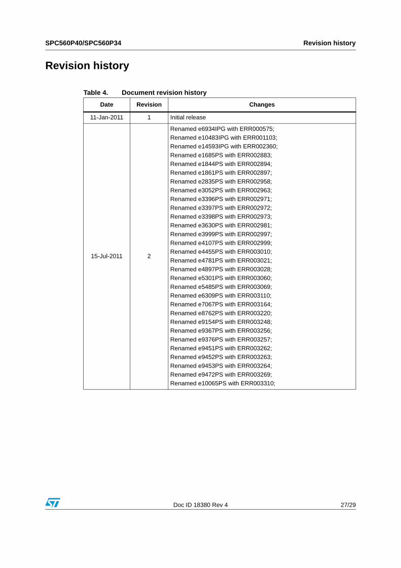
Revision history
Table 4. Document revision history
Date Revision Changes
11-Jan-2011 1 Initial release
15-Jul-2011 2
Renamed e6934IPG with ERR000575;Renamed e10483IPG with ERR001103;Renamed e14593IPG with ERR002360;
Renamed e1685PS with ERR002883;Renamed e1844PS with ERR002894;Renamed e1861PS with ERR002897;
Renamed e2835PS with ERR002958;Renamed e3052PS with ERR002963;Renamed e3396PS with ERR002971;
Renamed e3397PS with ERR002972;Renamed e3398PS with ERR002973;Renamed e3630PS with ERR002981;
Renamed e3999PS with ERR002997;Renamed e4107PS with ERR002999;Renamed e4455PS with ERR003010;
Renamed e4781PS with ERR003021;Renamed e4897PS with ERR003028;Renamed e5301PS with ERR003060;
Renamed e5485PS with ERR003069;Renamed e6309PS with ERR003110;Renamed e7067PS with ERR003164;
Renamed e8762PS with ERR003220;Renamed e9154PS with ERR003248;Renamed e9367PS with ERR003256;
Renamed e9376PS with ERR003257;Renamed e9451PS with ERR003262;Renamed e9452PS with ERR003263;
Renamed e9453PS with ERR003264;Renamed e9472PS with ERR003269;Renamed e10065PS with ERR003310;
SPC560P40/SPC560P34 Revision history
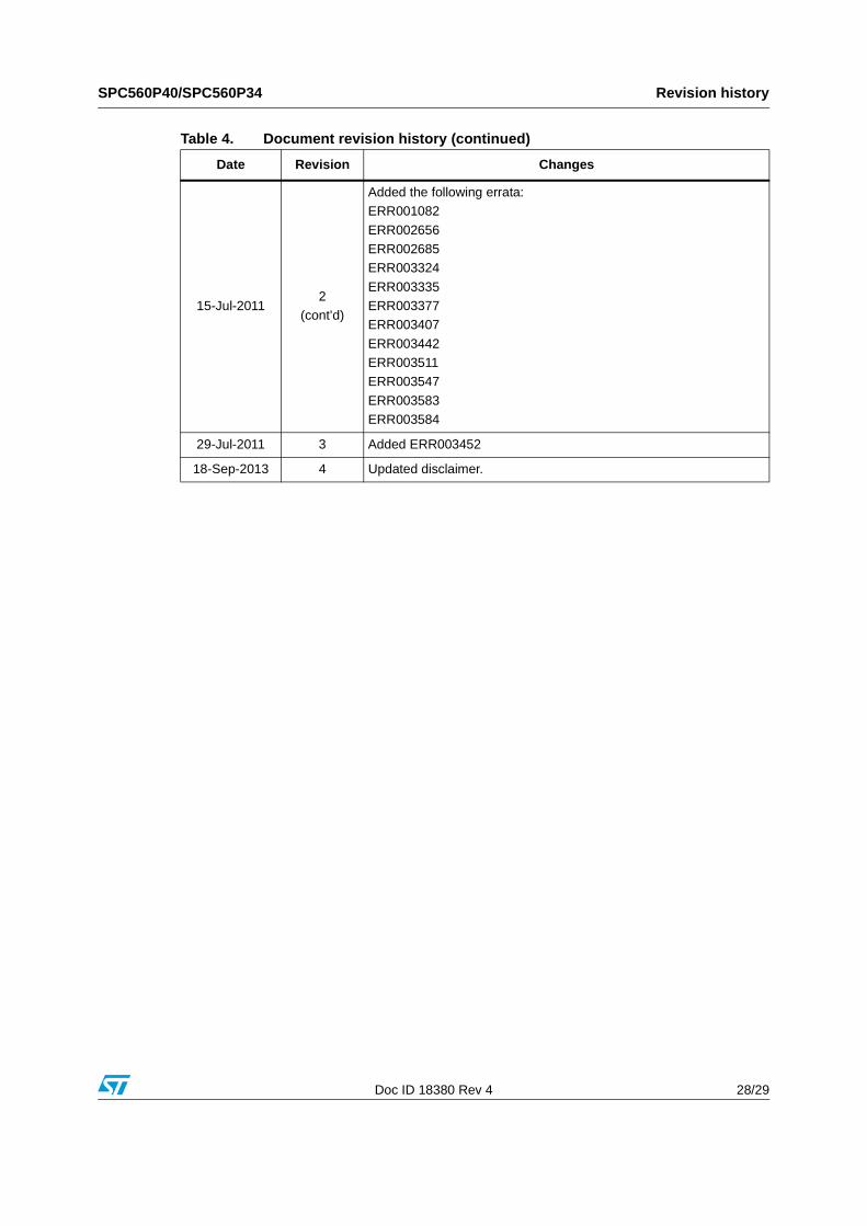
Doc ID 18380 Rev 4 28/29
15-Jul-20112
(cont’d)
Added the following errata:ERR001082
ERR002656ERR002685ERR003324
ERR003335ERR003377ERR003407
ERR003442ERR003511ERR003547
ERR003583ERR003584
29-Jul-2011 3 Added ERR003452
18-Sep-2013 4 Updated disclaimer.
Table 4. Document revision history (continued)
Date Revision Changes

SPC560P40/SPC560P34
Doc ID 18380 Rev 4 29/29
Please Read Carefully:
Information in this document is provided solely in connection with ST products. STMicroelectronics NV and its subsidiaries (“ST”) reserve theright to make changes, corrections, modifications or improvements, to this document, and the products and services described herein at anytime, without notice.
All ST products are sold pursuant to ST’s terms and conditions of sale.
Purchasers are solely responsible for the choice, selection and use of the ST products and services described herein, and ST assumes noliability whatsoever relating to the choice, selection or use of the ST products and services described herein.
No license, express or implied, by estoppel or otherwise, to any intellectual property rights is granted under this document. If any part of thisdocument refers to any third party products or services it shall not be deemed a license grant by ST for the use of such third party productsor services, or any intellectual property contained therein or considered as a warranty covering the use in any manner whatsoever of suchthird party products or services or any intellectual property contained therein.
UNLESS OTHERWISE SET FORTH IN ST’S TERMS AND CONDITIONS OF SALE ST DISCLAIMS ANY EXPRESS OR IMPLIED WARRANTY WITH RESPECT TO THE USE AND/OR SALE OF ST PRODUCTS INCLUDING WITHOUT LIMITATION IMPLIED WARRANTIES OF MERCHANTABILITY, FITNESS FOR A PARTICULAR PURPOSE (AND THEIR EQUIVALENTS UNDER THE LAWS OF ANY JURISDICTION), OR INFRINGEMENT OF ANY PATENT, COPYRIGHT OR OTHER INTELLECTUAL PROPERTY RIGHT.
ST PRODUCTS ARE NOT DESIGNED OR AUTHORIZED FOR USE IN: (A) SAFETY CRITICAL APPLICATIONS SUCH AS LIFE SUPPORTING, ACTIVE IMPLANTED DEVICES OR SYSTEMS WITH PRODUCT FUNCTIONAL SAFETY REQUIREMENTS; (B) AERONAUTIC APPLICATIONS; (C) AUTOMOTIVE APPLICATIONS OR ENVIRONMENTS, AND/OR (D) AEROSPACE APPLICATIONS OR ENVIRONMENTS. WHERE ST PRODUCTS ARE NOT DESIGNED FOR SUCH USE, THE PURCHASER SHALL USE PRODUCTS AT PURCHASER’S SOLE RISK, EVEN IF ST HAS BEEN INFORMED IN WRITING OF SUCH USAGE, UNLESS A PRODUCT IS EXPRESSLY DESIGNATED BY ST AS BEING INTENDED FOR “AUTOMOTIVE, AUTOMOTIVE SAFETY OR MEDICAL” INDUSTRY DOMAINS ACCORDING TO ST PRODUCT DESIGN SPECIFICATIONS. PRODUCTS FORMALLY ESCC, QML OR JAN QUALIFIED ARE DEEMED SUITABLE FOR USE IN AEROSPACE BY THE CORRESPONDING GOVERNMENTAL AGENCY.
Resale of ST products with provisions different from the statements and/or technical features set forth in this document shall immediately voidany warranty granted by ST for the ST product or service described herein and shall not create or extend in any manner whatsoever, anyliability of ST.
ST and the ST logo are trademarks or registered trademarks of ST in various countries.Information in this document supersedes and replaces all information previously supplied.
The ST logo is a registered trademark of STMicroelectronics. All other names are the property of their respective owners.
© 2013 STMicroelectronics - All rights reserved
STMicroelectronics group of companies
Australia - Belgium - Brazil - Canada - China - Czech Republic - Finland - France - Germany - Hong Kong - India - Israel - Italy - Japan - Malaysia - Malta - Morocco - Philippines - Singapore - Spain - Sweden - Switzerland - United Kingdom - United States of America
www.st.com