Embed Size (px)
Citation preview

Phys. Status Solidi A 206, No. 8, 1829–1832 (2009) / DOI 10.1002/pssa.200881594 p s sapplications and materials science
a
statu
s
soli
di
www.pss-a.comph
ysi
ca
Spatially resolved strain withina single SiGe island investigated by X-rayscanning microdiffractionAna Diaz*,1,2, Cristian Mocuta† ,1, Julian Stangl2, Joan Vila-Comamala3, Christian David3,Till H. Metzger1, and Gunther Bauer2
1 European Synchrotron Radiation Facility, 6 rue Jules Horowitz BP220, 38043 Grenoble Cedex, France2 Institute of Semiconductor and Solid State Physics, Johannes Kepler Universitat, Altenbergerstr. 69, 4040 Linz, Austria3 Paul Scherrer Institut, 5232 Villigen, Switzerland
Received 16 September 2008, revised 3 December 2008, accepted 5 March 2009Published online 23 June 2009
PACS 61.05.C−, 62.20.−x, 68.65.−k, 68.37.Yz
∗ Corresponding author: e-mail [email protected], Phone: +33 746 882473, Fax: +33 476 882160† Present address: Synchrotron Soleil, L’Orme des Merisiers, St. Aubin, BP 48, 91192 Gif-Sur-Yvette, France
A submicron X-ray beam was employed to scan a 3.2 �m SiGeisland in two directions. At each scanning position, 2D cuts ofthe reciprocal space close to the (004) Bragg reflection of theSi substrate were recorded with a CCD. From the position ofthe SiGe island induced diffuse scattering peak on each CCDframe, we detected and analyzed variations of the strain within aselected single island. Our method does not require the record-
ing of the whole 3D reciprocal space at each position in realspace, thus avoiding instability problems during data acquisi-tion. We found changes in the strain which are consistent withfinite element calculations of the strain within a model island.The knowledge of the strain distribution within SiGe epitax-ial structures is relevant for the correct interpretation of theirelectronic and optical properties.
© 2009 WILEY-VCH Verlag GmbH & Co. KGaA, Weinheim
1 Introduction The semiconductor industry isincreasingly interested in the development of semiconductornanostructures to be integrated in the minimization processof devices. The related strain-induced enhancement ofcharge carrier mobilities is an important step to improvethe performance of devices. The strain issue is one of thereasons why epitaxial growth of nanostructures like SiGeislands on Si is studied.
X-ray diffraction is the non-destructive technique ofchoice for the determination of size, shape, correlation dis-tances, and strain distribution within SiGe islands. Typically,a beam of a few hundred microns size is used to illumi-nate many of these structures simultaneously. Measurementsof the reciprocal space around a Bragg reflection are thencompared with calculations based on a model, determin-ing the ensemble average properties [1–4]. However, it oftenhappens, i.e., during self-organized growth, that the islandsexhibit a certain size distribution, resulting in a smearing ofthe diffraction patterns. This motivates the study of individualislands, for which a focused X-ray beam is needed in order to
compensate for the smaller diffraction volume given by a sin-gle nanostructure. When a single island is fully illuminatedby the beam, its individual properties and its variation fromisland to island can be studied in the same way as describedrecently [5].
One step further in the study of individual SiGe islandswas recently proposed by Hanke et al. [6], in which a 200 nmbeam was used to scan a 1 �m island in real space and record3D reciprocal space maps at each position. Apart from pro-viding a high flux, the focused beam acts in this case as ascanning probe within a single island, determining the reso-lution in real space. However, this method is time consumingand it is extremely sensitive to instabilities in the experi-mental setup, such as mechanical drifts and vibrations in thesample and/or in the beam. In this work we exploit this tech-nique by only taking 2D cuts of the reciprocal space witha CCD, in such a way that only a single measurement isrequired at each scanning step. We show that, when choosingan appropriate deviation from the Bragg angle of the sample,2D reciprocal space cuts are sufficient for determining strain
© 2009 WILEY-VCH Verlag GmbH & Co. KGaA, Weinheim
1830 A. Diaz et al.: Spatially resolved strain within a SiGe island
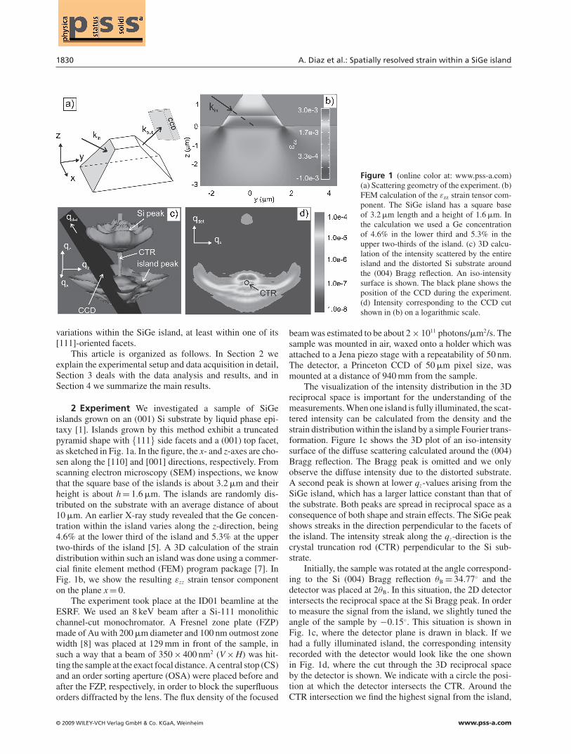
Figure 1 (online color at: www.pss-a.com)(a) Scattering geometry of the experiment. (b)FEM calculation of the εzz strain tensor com-ponent. The SiGe island has a square baseof 3.2 �m length and a height of 1.6 �m. Inthe calculation we used a Ge concentrationof 4.6% in the lower third and 5.3% in theupper two-thirds of the island. (c) 3D calcu-lation of the intensity scattered by the entireisland and the distorted Si substrate aroundthe (004) Bragg reflection. An iso-intensitysurface is shown. The black plane shows theposition of the CCD during the experiment.(d) Intensity corresponding to the CCD cutshown in (b) on a logarithmic scale.
variations within the SiGe island, at least within one of its[111]-oriented facets.
This article is organized as follows. In Section 2 weexplain the experimental setup and data acquisition in detail,Section 3 deals with the data analysis and results, and inSection 4 we summarize the main results.
2 Experiment We investigated a sample of SiGeislands grown on an (001) Si substrate by liquid phase epi-taxy [1]. Islands grown by this method exhibit a truncatedpyramid shape with {111} side facets and a (001) top facet,as sketched in Fig. 1a. In the figure, the x- and z-axes are cho-sen along the [110] and [001] directions, respectively. Fromscanning electron microscopy (SEM) inspections, we knowthat the square base of the islands is about 3.2 �m and theirheight is about h = 1.6 �m. The islands are randomly dis-tributed on the substrate with an average distance of about10 �m. An earlier X-ray study revealed that the Ge concen-tration within the island varies along the z-direction, being4.6% at the lower third of the island and 5.3% at the uppertwo-thirds of the island [5]. A 3D calculation of the straindistribution within such an island was done using a commer-cial finite element method (FEM) program package [7]. InFig. 1b, we show the resulting εzz strain tensor componenton the plane x = 0.
The experiment took place at the ID01 beamline at theESRF. We used an 8 keV beam after a Si-111 monolithicchannel-cut monochromator. A Fresnel zone plate (FZP)made of Au with 200 �m diameter and 100 nm outmost zonewidth [8] was placed at 129 mm in front of the sample, insuch a way that a beam of 350 × 400 nm2 (V × H) was hit-ting the sample at the exact focal distance. A central stop (CS)and an order sorting aperture (OSA) were placed before andafter the FZP, respectively, in order to block the superfluousorders diffracted by the lens. The flux density of the focused
beam was estimated to be about 2 × 10¹¹ photons/�m2/s. Thesample was mounted in air, waxed onto a holder which wasattached to a Jena piezo stage with a repeatability of 50 nm.The detector, a Princeton CCD of 50 �m pixel size, wasmounted at a distance of 940 mm from the sample.
The visualization of the intensity distribution in the 3Dreciprocal space is important for the understanding of themeasurements. When one island is fully illuminated, the scat-tered intensity can be calculated from the density and thestrain distribution within the island by a simple Fourier trans-formation. Figure 1c shows the 3D plot of an iso-intensitysurface of the diffuse scattering calculated around the (004)Bragg reflection. The Bragg peak is omitted and we onlyobserve the diffuse intensity due to the distorted substrate.A second peak is shown at lower qz-values arising from theSiGe island, which has a larger lattice constant than that ofthe substrate. Both peaks are spread in reciprocal space as aconsequence of both shape and strain effects. The SiGe peakshows streaks in the direction perpendicular to the facets ofthe island. The intensity streak along the qz-direction is thecrystal truncation rod (CTR) perpendicular to the Si sub-strate.
Initially, the sample was rotated at the angle correspond-ing to the Si (004) Bragg reflection θB = 34.77◦ and thedetector was placed at 2θB. In this situation, the 2D detectorintersects the reciprocal space at the Si Bragg peak. In orderto measure the signal from the island, we slightly tuned theangle of the sample by −0.15◦. This situation is shown inFig. 1c, where the detector plane is drawn in black. If wehad a fully illuminated island, the corresponding intensityrecorded with the detector would look like the one shownin Fig. 1d, where the cut through the 3D reciprocal spaceby the detector is shown. We indicate with a circle the posi-tion at which the detector intersects the CTR. Around theCTR intersection we find the highest signal from the island,
© 2009 WILEY-VCH Verlag GmbH & Co. KGaA, Weinheim www.pss-a.com
Original
Paper
Phys. Status Solidi A 206, No. 8 (2009) 1831
corresponding to the streak from the front facet, which ishighlighted in gray in Fig. 1a. At both sides from this signalwe observe the intersection with the streaks from the lateralfacets. Finally, at high qz-values, we intersect the signal aris-ing from the part of the Si substrate below the front facet ofthe island.
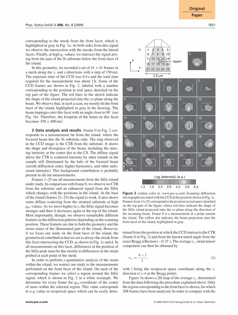
In this geometry, we recorded a set of 41 × 41 frames ina mesh along the x- and y-directions with a step of 150 nm.The exposure time of the CCD was 0.4 s and the total timerequired for the measurement was about 1 h. Some of theCCD frames are shown in Fig. 2, labeled with a numbercorresponding to the position in real space sketched on thetop part of the figure. The red lines in the sketch indicatethe shape of the island projected onto the xy-plane along thebeam. We observe that, in such a scan, we mostly hit the frontfacet of the island, highlighted in gray in the drawing. Thebeam impinges onto this facet with an angle close to 90◦ (seeFig. 1b). Therefore, the footprint of the beam on this facetbecomes 350 × 400 nm2.
3 Data analysis and results Frame 0 in Fig. 2 cor-responds to a measurement far from the island, where thefocused beam hits the Si substrate only. The ring observedin the CCD image is the CTR from the substrate. It showsthe shape and divergence of the beam, including the miss-ing intensity at the center due to the CS. The diffuse signalabove the CTR is scattered intensity by other islands in thesample still illuminated by the halo of the focused beam(zeroth diffraction order, higher harmonics, and other unfo-cused intensity). This background contribution is probablypresent in all our measurements.
Frames 1–25 are all measurements from the SiGe islandunder study. In comparison with frame 0, we observe no CTRfrom the substrate and an enhanced signal from the SiGewhich changes with the positions in the island. At the baseof the island (frames 21–25) the signal is weak. It also showssome diffuse scattering from the strained substrate at highqdet-values. As we move higher in y, the SiGe signal becomesstronger and then it decreases again at the top of the island.Most importantly, though, we observe remarkable differentfeatures in the diffraction patterns depending on the scanningposition. These features are due to both the geometry and thestrain states of the illuminated part of the island. However,if we focus our study on the front facet of the island, thegeometrical contribution that we see is always the streak fromthis facet intersecting the CCD, as shown in Fig. 1c and d. Inall measurements on this facet, differences in the position ofthe SiGe peak must be due mostly to differences in the strainprobed at each point of the mesh.
In order to perform a quantitative analysis of the strainwithin the island, we restrict our study to the measurementsperformed on the front facet of the island. On each of thecorresponding frames we select a region around the SiGesignal, which is shown in Fig. 2 in a white rectangle. Wedetermine for every frame the qdet-coordinate of the centerof mass within the selected region. This value correspondsto a qz-value in reciprocal space which can be easily deter-
Figure 2 (online color at: www.pss-a.com) Scanning diffractionmicrographs recorded with the CCD at the position shown in Fig. 1c.Frames from 1 to 25 correspond to the position in real space sketchedon the top part of the figure, where red lines indicate the shape ofthe SiGe island projected onto the xy-plane along the direction ofthe incoming beam. Frame 0 is a measurement at a point outsidethe island. The yellow dot indicates the beam projection onto thefront facet of the island, highlighted in gray.
mined from the position at which the CCD intersects the CTR(frame 0 in Fig. 2) and from the known tuned angle from theexact Bragg reflection (−0.15◦). The average εzz strain tensorcomponent can then be obtained by
εzz = 4 − l
l, (1)
with l being the reciprocal space coordinate along the z-direction (l = 4 at the Bragg point).
Figure 3a shows a 2D map of the average εzz determinedfrom the data following the procedure explained above. Onlythe region corresponding to the front facet is shown, for which308 frames have been analyzed. In order to compare with the
www.pss-a.com © 2009 WILEY-VCH Verlag GmbH & Co. KGaA, Weinheim

1832 A. Diaz et al.: Spatially resolved strain within a SiGe island
Figure 3 (online color at: www.pss-a.com)(a) εzz strain tensor component extracted fromthe measured diffraction patterns shown inFig. 2 at different scanning positions on the xy-plane. Only the scanned region correspondingto the front facet is shown. (b) Average εzz
along the incoming beam through the SiGeisland from a 3D FEM calculation. The scalein (a) is shifted by 4.0 × 10⁻⁴ with respect tothe scale in (b). Both scales have the samerange.
expected εzz-values, we calculate the average strain alongthe beam direction projected onto the xy-plane (see Fig. 3b)from the 3D FEM calculation shown in Fig. 1b. The scalesin both maps of Fig. 3 have the same range, but measuredvalues have an offset of 4.0 × 10⁻⁴ with respect to the cal-culation. Apart from this offset, the main trends observed inthe measurement follow the expected ones: the strain is max-imum at the central part of the island and lower at the bottom,especially at the lower corners. In the lower part, variationsalong the x-direction have a maximum at the center, whileon the upper part they are more or less constant. Finally,the scale ranges in both measurement and calculation arethe same, indicating that the measured strain variations arerealistic.
On the top part of the facet (high y-values), strain valuesseem to be higher at the edges of the facet. We believe thatthese are effects arising from the fact that the lateral facetsare close, introducing different geometrical contributions inthe diffracted signal. Finally, asymmetries in the measuredstrain map with respect to the x-direction can be explainedby a misalignment of the island with respect to the incomingbeam. The sample was aligned by eye in such a way thatthe x-axis is perpendicular to the beam with an error of ±5◦.We also observe an asymmetry in the scanning diffractionmicrographs of Fig. 2.
4 Conclusion We used a submicron focused beam asa probe to scan a 3.2 �m SiGe island in a mesh alongits Si substrate. At each point of the mesh, we took CCDimages intersecting the 3D reciprocal space close to the(004) Bragg reflection. By tracking the position of theSiGe peak we mapped the average εzz strain tensor com-ponent along the X-ray beam. The strain map obtainedwithin the front facet of the island is consistent with FEMcalculations except for an offset which might be due togeometrical effects. The advantage of our method lies on
the simplicity of the data acquisition, since it is not neces-sary to perform a whole 3D reciprocal space map at eachmeshing point. This reduces the measuring time and it isless sensitive to drifts and vibrations in the experimentalsetup.
In the future we plan to perform a more accurate quan-titative study of the strain by performing FEM calculationsof the different illuminated parts of the sample in order todisentangle shape and strain contributions in the diffractionpatterns. We also plan to improve the mechanical stabilityin the setup, which will allow smaller probe sizes and thussmaller samples to be analyzed.
Acknowledgements We would like to thank MartinSchmidbauer for providing the sample and Hamid Djazouli fortechnical support during the measurements.
References
[1] M. Schmidbauer, X-ray Diffuse Scattering from Self-organized Mesoscopic Semiconductor Structures (Springer-Verlag, Berlin, Heidelberg, 2004).
[2] M. Schmidbauer, M. Hanke, and R. Hohler, Cryst. Res. Tech-nol. 37, 3 (2002).
[3] T. Wiebach, M. Schmidbauer, M. Hanke, H. Raidt, R. Kohler,and H. Wawra, Phys. Rev. B 61, 5571 (2000).
[4] A. Hesse, J. Stangl, V. Holy, T. Roch, G. Bauer, O. G. Schmidt,U. Denker, and B. Struth, Phys. Rev. B 66, 085321 (2000).
[5] C. Mocuta, J. Stangl, K. Mundboth, T. H. Metzger, G. Bauer,I. A. Vartanyants, M. Schmidbauer, and T. Boeck, Phys. Rev.B 77, 245425 (2008).
[6] M. Hanke, M. Dubslaff, M. Schmidbauer, T. Boeck, S.Schroder, M. Burghammer, C. Riekel, J. Patommel, and C.G. Schoer, Appl. Phys. Lett. 77, 193109 (2008).
[7] Comsol Multiphysics with structural mechanics module,www.comsol.com.
[8] K. Jefimovs, O. Bunk, F. Pfeiffer, D. Grolimund, J. F. van derVeen, and C. David, Microelectron. Eng. 84, 1467 (2007).
© 2009 WILEY-VCH Verlag GmbH & Co. KGaA, Weinheim www.pss-a.com