Embed Size (px)
Citation preview

Spansion® Analog and Microcontroller Products The following document contains information on Spansion analog and microcontroller products. Although the document is marked with the name “Fujitsu”, the company that originally developed the specification, Spansion will continue to offer these products to new and existing customers. Continuity of Specifications There is no change to this document as a result of offering the device as a Spansion product. Any changes that have been made are the result of normal document improvements and are noted in the document revision summary, where supported. Future routine revisions will occur when appropriate, and changes will be noted in a revision summary. Continuity of Ordering Part Numbers Spansion continues to support existing part numbers beginning with “MB”. To order these products, please use only the Ordering Part Numbers listed in this document. For More Information Please contact your local sales office for additional information about Spansion memory, analog, and microcontroller products and solutions.

FUJITSU SEMICONDUCTORDATA SHEET DS04-27262-4E
ASSP for Power Management Applications (General-Purpose DC/DC Converter)2ch PFM/PWM DC/DC converter IC with synchronous rectification
MB39A136■ DESCRIPTION
MB39A136 is 2ch step-down DC/DC converter IC of the current mode N-ch/N-ch synchronous rectificationmethod. It contains the enhanced protection features, and supports the symmetrical-phase method and theceramic capacitor. MB39A136 realizes rapid response, high efficiency, and low ripple voltage, and its high-frequency operation enables the miniaturization of inductors and I/O capacitors.
■ FEATURES• High efficiency• For frequency setting by external resistor : 100 kHz to 1 MHz• Error Amp threshold voltage : 0.7 V ± 1.0%• Minimum output voltage value : 0.7 V• Wide range of power-supply voltage : 4.5 V to 25 V• PFM/PWM auto switching mode and fixed PWM mode selectable• Supports Symmetrical-Phase method• With built-in over voltage protection function• With built-in under voltage protection function• With built-in over current protection function• With built-in over-temperature protection function• With built-in soft start/stop circuit without load dependence• With built-in synchronous rectification type output steps for N-ch MOS FET• Standby current : 0 [μA] Typ• Small package : TSSOP-24
■ APPLICATION• Digital TV• Photocopiers• Surveillance cameras• Set-top boxes (STB)• DVD players, DVD recorders• Projectors• IP phones• Vending machine• Consoles and other non-portable devices
Copyright©2008-2013 FUJITSU SEMICONDUCTOR LIMITED All rights reserved2013.1
MB39A136
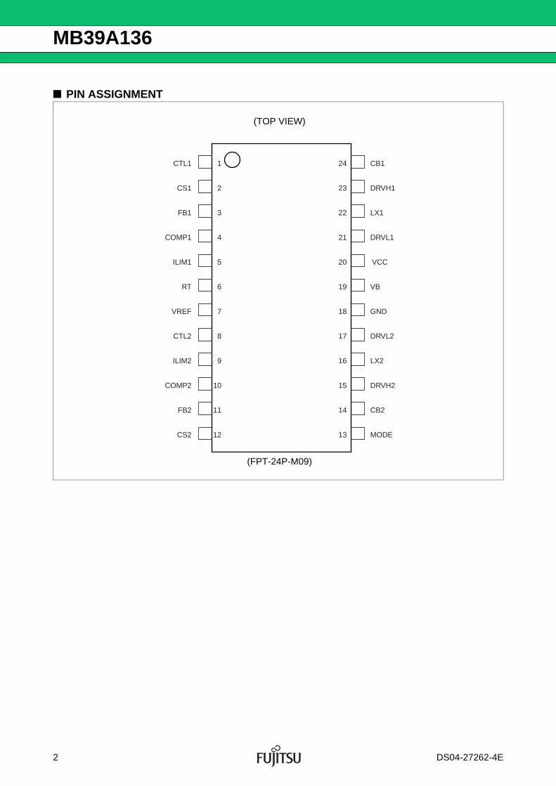
■ PIN ASSIGNMENT
(TOP VIEW)
(FPT-24P-M09)
24
23
22
21
20
19
18
17
16 LX2
15
14
13
CB1
DRVH1
LX1
DRVL1
VCC
VB
GND
DRVL2
DRVH2
CB2
MODE
1
2
3
4
5
6
7
8
9
10
11
12
CTL1
CS1
FB1
COMP1
ILIM1
RT
VREF
CTL2
ILIM2
COMP2
FB2
CS2
2 DS04-27262-4E
MB39A136
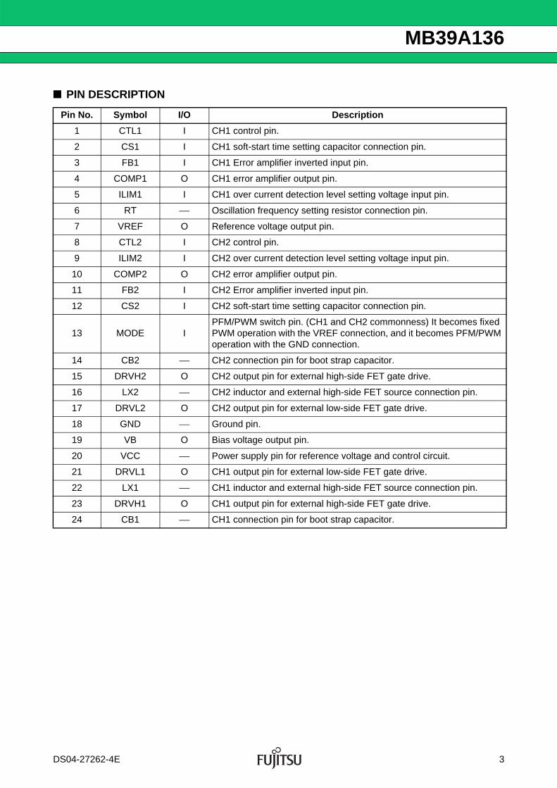
■ PIN DESCRIPTION
Pin No. Symbol I/O Description
1 CTL1 I CH1 control pin.
2 CS1 I CH1 soft-start time setting capacitor connection pin.
3 FB1 I CH1 Error amplifier inverted input pin.
4 COMP1 O CH1 error amplifier output pin.
5 ILIM1 I CH1 over current detection level setting voltage input pin.
6 RT ⎯ Oscillation frequency setting resistor connection pin.
7 VREF O Reference voltage output pin.
8 CTL2 I CH2 control pin.
9 ILIM2 I CH2 over current detection level setting voltage input pin.
10 COMP2 O CH2 error amplifier output pin.
11 FB2 I CH2 Error amplifier inverted input pin.
12 CS2 I CH2 soft-start time setting capacitor connection pin.
13 MODE IPFM/PWM switch pin. (CH1 and CH2 commonness) It becomes fixed PWM operation with the VREF connection, and it becomes PFM/PWM operation with the GND connection.
14 CB2 ⎯ CH2 connection pin for boot strap capacitor.
15 DRVH2 O CH2 output pin for external high-side FET gate drive.
16 LX2 ⎯ CH2 inductor and external high-side FET source connection pin.
17 DRVL2 O CH2 output pin for external low-side FET gate drive.
18 GND ⎯ Ground pin.
19 VB O Bias voltage output pin.
20 VCC ⎯ Power supply pin for reference voltage and control circuit.
21 DRVL1 O CH1 output pin for external low-side FET gate drive.
22 LX1 ⎯ CH1 inductor and external high-side FET source connection pin.
23 DRVH1 O CH1 output pin for external high-side FET gate drive.
24 CB1 ⎯ CH1 connection pin for boot strap capacitor.
DS04-27262-4E 3
MB39A136
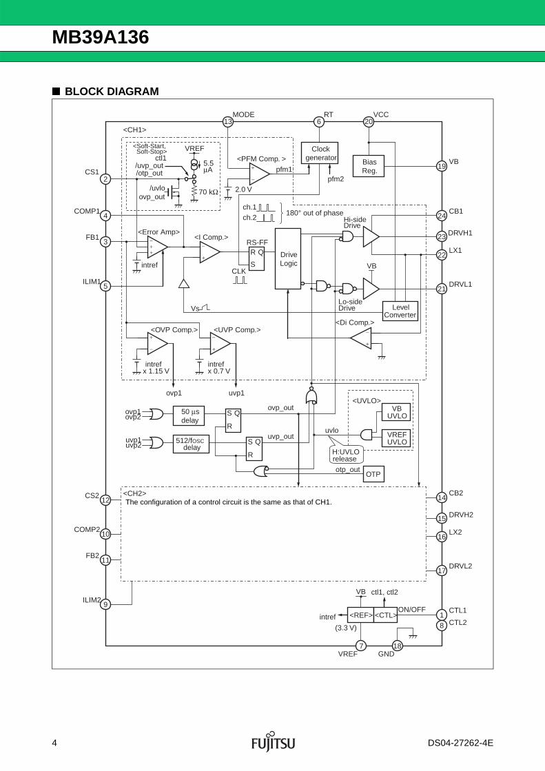
■ BLOCK DIAGRAM
+
−
−
++ −
+
+
−
−
+
−
+
FB1
COMP1
CS1
CS2
COMP2
FB2
ILIM1
ILIM2
3
4
2
11
10
12
5
9
5.5μA
VREF<Soft-Start, Soft-Stop>
/uvloovp_out
<CH1>13
MODE
70 kΩ
ctl1/uvp_out/otp_out
intref
<I Comp.><Error Amp>
ovp1
intrefx 0.7 V
intrefx 1.15 V
<OVP Comp.>
uvp1
<UVP Comp.>
Vs
ovp1ovp2
<CH2>
uvp1uvp2
50 μsdelay
512/fOSCdelay
ovp_out
uvp_outS Q
R
S Q
R
VBUVLO
<UVLO>
VREFUVLO
uvlo
H:UVLOrelease
OTPotp_out
DriveLogic
Hi-sideDrive
BiasReg.
RS-FF
20VCC
S
QR
Clockgenerator
ch.1180° out of phase
6RT
ch.2
<PFM Comp. >pfm1
pfm22.0 V
CLKVB
Lo-sideDrive Level
Converter<Di Comp.>
23
22
24CB1
DRVH1
LX1
19VB
21DRVL1
1
15
16
14
17
CB2
DRVH2
DRVL2
LX2
CTL1
CTL28<REF> <CTL>intref
(3.3 V)
7 18
ON/OFF
VB
GNDVREF
ctl1, ctl2
The configuration of a control circuit is the same as that of CH1.
4 DS04-27262-4E
MB39A136
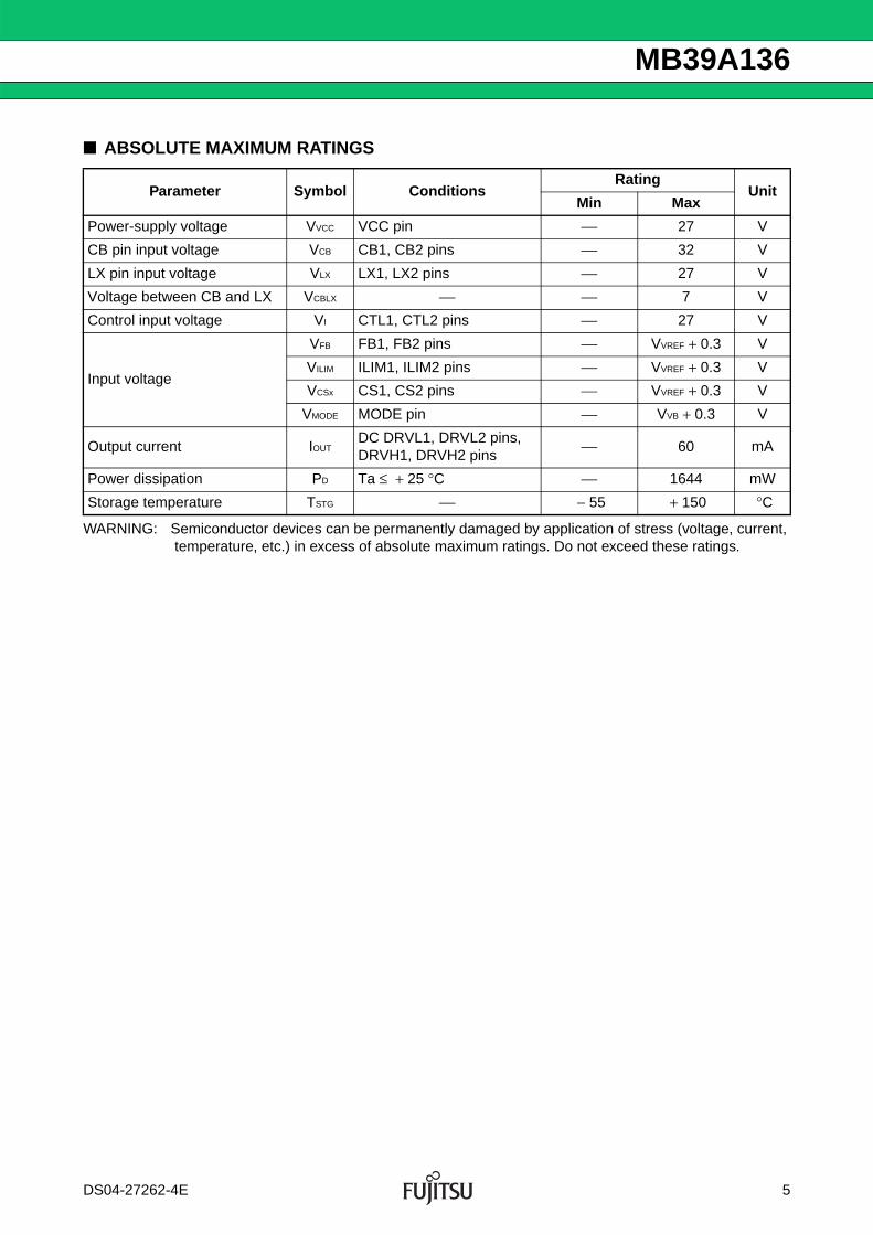
■ ABSOLUTE MAXIMUM RATINGS
WARNING: Semiconductor devices can be permanently damaged by application of stress (voltage, current, temperature, etc.) in excess of absolute maximum ratings. Do not exceed these ratings.
Parameter Symbol ConditionsRating
UnitMin Max
Power-supply voltage VVCC VCC pin ⎯ 27 V
CB pin input voltage VCB CB1, CB2 pins ⎯ 32 V
LX pin input voltage VLX LX1, LX2 pins ⎯ 27 V
Voltage between CB and LX VCBLX ⎯ ⎯ 7 V
Control input voltage VI CTL1, CTL2 pins ⎯ 27 V
Input voltage
VFB FB1, FB2 pins ⎯ VVREF + 0.3 V
VILIM ILIM1, ILIM2 pins ⎯ VVREF + 0.3 V
VCSx CS1, CS2 pins ⎯ VVREF + 0.3 V
VMODE MODE pin ⎯ VVB + 0.3 V
Output current IOUTDC DRVL1, DRVL2 pins, DRVH1, DRVH2 pins
⎯ 60 mA
Power dissipation PD Ta ≤ + 25 °C ⎯ 1644 mW
Storage temperature TSTG ⎯ − 55 + 150 °C
DS04-27262-4E 5
MB39A136
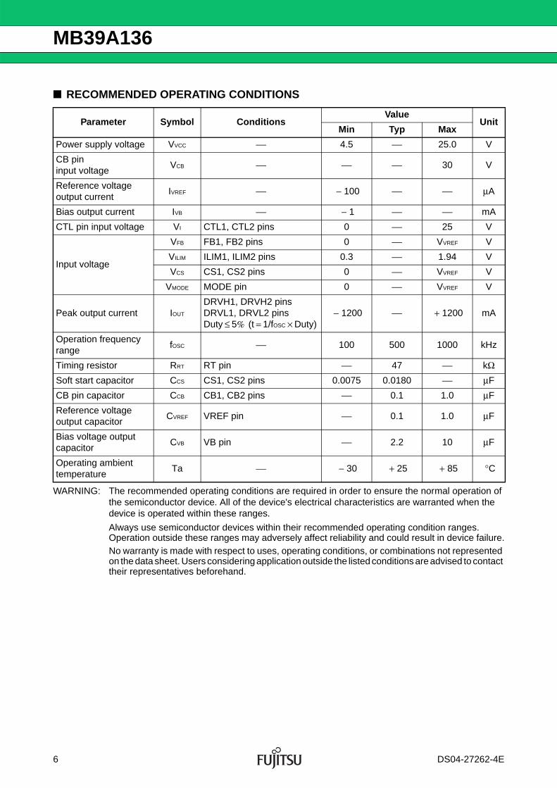
■ RECOMMENDED OPERATING CONDITIONS
WARNING: The recommended operating conditions are required in order to ensure the normal operation of the semiconductor device. All of the device's electrical characteristics are warranted when the device is operated within these ranges.
Always use semiconductor devices within their recommended operating condition ranges. Operation outside these ranges may adversely affect reliability and could result in device failure.No warranty is made with respect to uses, operating conditions, or combinations not represented on the data sheet. Users considering application outside the listed conditions are advised to contact their representatives beforehand.
Parameter Symbol ConditionsValue
UnitMin Typ Max
Power supply voltage VVCC ⎯ 4.5 ⎯ 25.0 V
CB pin input voltage
VCB ⎯ ⎯ ⎯ 30 V
Reference voltage output current
IVREF ⎯ − 100 ⎯ ⎯ μA
Bias output current IVB ⎯ − 1 ⎯ ⎯ mA
CTL pin input voltage VI CTL1, CTL2 pins 0 ⎯ 25 V
Input voltage
VFB FB1, FB2 pins 0 ⎯ VVREF V
VILIM ILIM1, ILIM2 pins 0.3 ⎯ 1.94 V
VCS CS1, CS2 pins 0 ⎯ VVREF V
VMODE MODE pin 0 ⎯ VVREF V
Peak output current IOUT
DRVH1, DRVH2 pinsDRVL1, DRVL2 pinsDuty ≤ 5% (t = 1/fOSC × Duty)
− 1200 ⎯ + 1200 mA
Operation frequency range
fOSC ⎯ 100 500 1000 kHz
Timing resistor RRT RT pin ⎯ 47 ⎯ kΩSoft start capacitor CCS CS1, CS2 pins 0.0075 0.0180 ⎯ μF
CB pin capacitor CCB CB1, CB2 pins ⎯ 0.1 1.0 μF
Reference voltage output capacitor
CVREF VREF pin ⎯ 0.1 1.0 μF
Bias voltage output capacitor
CVB VB pin ⎯ 2.2 10 μF
Operating ambient temperature
Ta ⎯ − 30 + 25 + 85 °C
6 DS04-27262-4E
MB39A136
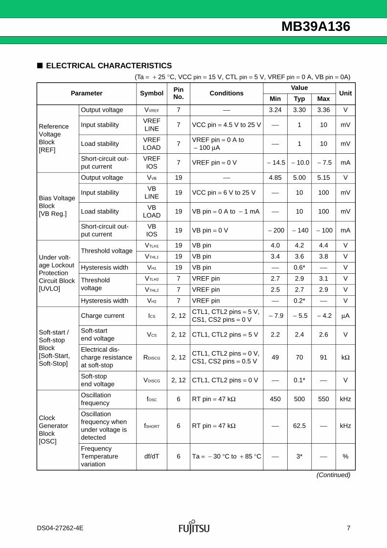
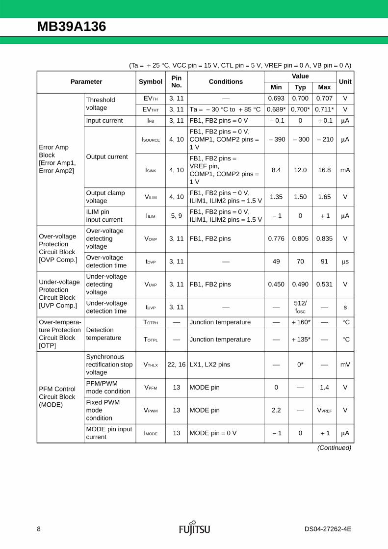
■ ELECTRICAL CHARACTERISTICS (Ta = + 25 °C, VCC pin = 15 V, CTL pin = 5 V, VREF pin = 0 A, VB pin = 0A)
(Continued)
Parameter Symbol Pin No. Conditions
ValueUnit
Min Typ Max
Reference Voltage Block[REF]
Output voltage VVREF 7 ⎯ 3.24 3.30 3.36 V
Input stabilityVREFLINE
7 VCC pin = 4.5 V to 25 V ⎯ 1 10 mV
Load stabilityVREFLOAD
7VREF pin = 0 A to − 100 μA
⎯ 1 10 mV
Short-circuit out-put current
VREFIOS
7 VREF pin = 0 V − 14.5 − 10.0 − 7.5 mA
Bias Voltage Block[VB Reg.]
Output voltage VVB 19 ⎯ 4.85 5.00 5.15 V
Input stabilityVB
LINE19 VCC pin = 6 V to 25 V ⎯ 10 100 mV
Load stabilityVB
LOAD19 VB pin = 0 A to − 1 mA ⎯ 10 100 mV
Short-circuit out-put current
VBIOS
19 VB pin = 0 V − 200 − 140 − 100 mA
Under volt-age Lockout Protection Circuit Block[UVLO]
Threshold voltageVTLH1 19 VB pin 4.0 4.2 4.4 V
VTHL1 19 VB pin 3.4 3.6 3.8 V
Hysteresis width VH1 19 VB pin ⎯ 0.6* ⎯ V
Threshold voltage
VTLH2 7 VREF pin 2.7 2.9 3.1 V
VTHL2 7 VREF pin 2.5 2.7 2.9 V
Hysteresis width VH2 7 VREF pin ⎯ 0.2* ⎯ V
Soft-start / Soft-stop Block [Soft-Start, Soft-Stop]
Charge current ICS 2, 12CTL1, CTL2 pins = 5 V, CS1, CS2 pins = 0 V
− 7.9 − 5.5 − 4.2 μA
Soft-start end voltage
VCS 2, 12 CTL1, CTL2 pins = 5 V 2.2 2.4 2.6 V
Electrical dis-charge resistance at soft-stop
RDISCG 2, 12CTL1, CTL2 pins = 0 V, CS1, CS2 pins = 0.5 V
49 70 91 kΩ
Soft-stop end voltage
VDISCG 2, 12 CTL1, CTL2 pins = 0 V ⎯ 0.1* ⎯ V
Clock Generator Block[OSC]
Oscillation frequency
fOSC 6 RT pin = 47 kΩ 450 500 550 kHz
Oscillation frequency when under voltage is detected
fSHORT 6 RT pin = 47 kΩ ⎯ 62.5 ⎯ kHz
Frequency Temperature variation
df/dT 6 Ta = − 30 °C to + 85 °C ⎯ 3* ⎯ %
DS04-27262-4E 7
MB39A136
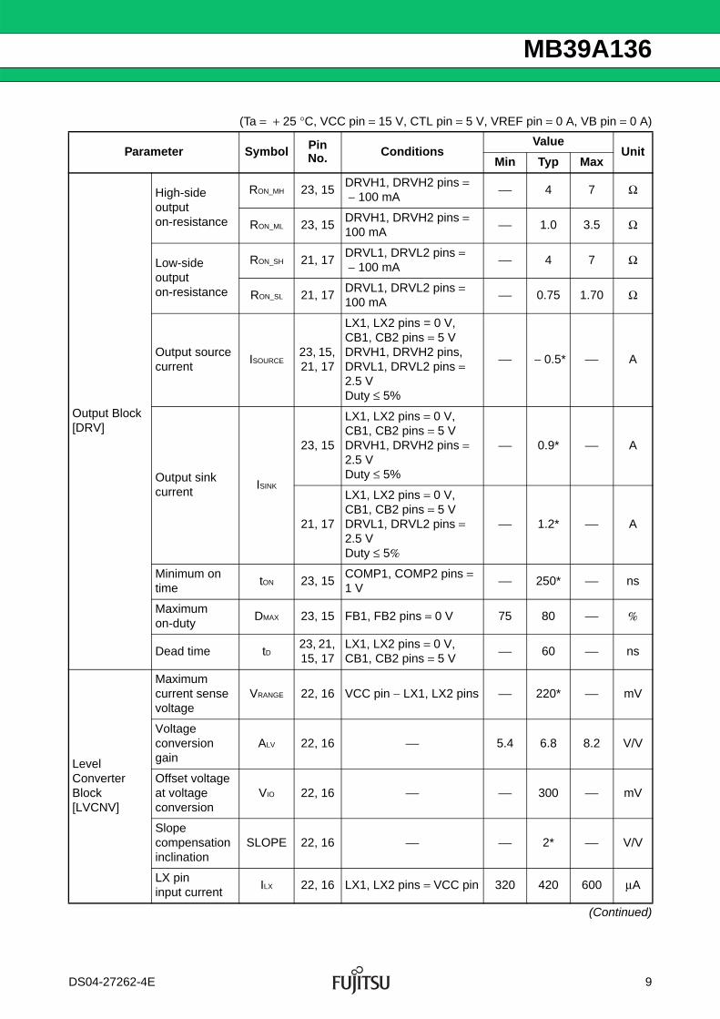
(Ta = + 25 °C, VCC pin = 15 V, CTL pin = 5 V, VREF pin = 0 A, VB pin = 0 A)
(Continued)
Parameter Symbol Pin No. Conditions
ValueUnit
Min Typ Max
Error Amp Block[Error Amp1, Error Amp2]
Threshold voltage
EVTH 3, 11 ⎯ 0.693 0.700 0.707 V
EVTHT 3, 11 Ta = − 30 °C to + 85 °C 0.689* 0.700* 0.711* V
Input current IFB 3, 11 FB1, FB2 pins = 0 V − 0.1 0 + 0.1 μA
Output current
ISOURCE 4, 10FB1, FB2 pins = 0 V, COMP1, COMP2 pins = 1 V
− 390 − 300 − 210 μA
ISINK 4, 10
FB1, FB2 pins = VREF pin, COMP1, COMP2 pins = 1 V
8.4 12.0 16.8 mA
Output clamp voltage
VILIM 4, 10FB1, FB2 pins = 0 V, ILIM1, ILIM2 pins = 1.5 V
1.35 1.50 1.65 V
ILIM pin input current
IILIM 5, 9FB1, FB2 pins = 0 V, ILIM1, ILIM2 pins = 1.5 V
− 1 0 + 1 μA
Over-voltage Protection Circuit Block[OVP Comp.]
Over-voltage detecting voltage
VOVP 3, 11 FB1, FB2 pins 0.776 0.805 0.835 V
Over-voltage detection time
tOVP 3, 11 ⎯ 49 70 91 μs
Under-voltage Protection Circuit Block[UVP Comp.]
Under-voltage detecting voltage
VUVP 3, 11 FB1, FB2 pins 0.450 0.490 0.531 V
Under-voltage detection time
tUVP 3, 11 ⎯ ⎯ 512/fOSC
⎯ s
Over-tempera-ture Protection Circuit Block[OTP]
Detection temperature
TOTPH ⎯ Junction temperature ⎯ + 160* ⎯ °C
TOTPL ⎯ Junction temperature ⎯ + 135* ⎯ °C
PFM Control Circuit Block (MODE)
Synchronous rectification stop voltage
VTHLX 22, 16 LX1, LX2 pins ⎯ 0* ⎯ mV
PFM/PWM mode condition
VPFM 13 MODE pin 0 ⎯ 1.4 V
Fixed PWM mode condition
VPWM 13 MODE pin 2.2 ⎯ VVREF V
MODE pin input current
IMODE 13 MODE pin = 0 V − 1 0 + 1 μA
8 DS04-27262-4E
MB39A136
(Ta = + 25 °C, VCC pin = 15 V, CTL pin = 5 V, VREF pin = 0 A, VB pin = 0 A)
(Continued)
Parameter Symbol Pin No. Conditions
ValueUnit
Min Typ Max
Output Block[DRV]
High-side output on-resistance
RON_MH 23, 15DRVH1, DRVH2 pins = − 100 mA
⎯ 4 7 Ω
RON_ML 23, 15DRVH1, DRVH2 pins = 100 mA
⎯ 1.0 3.5 Ω
Low-side output on-resistance
RON_SH 21, 17DRVL1, DRVL2 pins = − 100 mA
⎯ 4 7 Ω
RON_SL 21, 17DRVL1, DRVL2 pins = 100 mA
⎯ 0.75 1.70 Ω
Output source current
ISOURCE23, 15, 21, 17
LX1, LX2 pins = 0 V, CB1, CB2 pins = 5 VDRVH1, DRVH2 pins, DRVL1, DRVL2 pins = 2.5 V Duty ≤ 5%
⎯ − 0.5* ⎯ A
Output sink current
ISINK
23, 15
LX1, LX2 pins = 0 V, CB1, CB2 pins = 5 VDRVH1, DRVH2 pins = 2.5 VDuty ≤ 5%
⎯ 0.9* ⎯ A
21, 17
LX1, LX2 pins = 0 V, CB1, CB2 pins = 5 VDRVL1, DRVL2 pins = 2.5 VDuty ≤ 5%
⎯ 1.2* ⎯ A
Minimum on time
tON 23, 15COMP1, COMP2 pins = 1 V
⎯ 250* ⎯ ns
Maximum on-duty
DMAX 23, 15 FB1, FB2 pins = 0 V 75 80 ⎯ %
Dead time tD23, 21, 15, 17
LX1, LX2 pins = 0 V, CB1, CB2 pins = 5 V
⎯ 60 ⎯ ns
Level Converter Block[LVCNV]
Maximum current sense voltage
VRANGE 22, 16 VCC pin − LX1, LX2 pins ⎯ 220* ⎯ mV
Voltage conversion gain
ALV 22, 16 ⎯ 5.4 6.8 8.2 V/V
Offset voltage at voltage conversion
VIO 22, 16 ⎯ ⎯ 300 ⎯ mV
Slope compensation inclination
SLOPE 22, 16 ⎯ ⎯ 2* ⎯ V/V
LX pin input current
ILX 22, 16 LX1, LX2 pins = VCC pin 320 420 600 μA
DS04-27262-4E 9
MB39A136
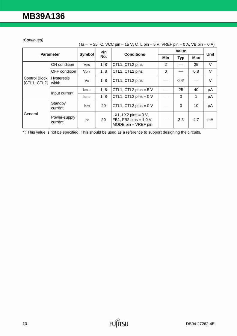
(Continued) (Ta = + 25 °C, VCC pin = 15 V, CTL pin = 5 V, VREF pin = 0 A, VB pin = 0 A)
* : This value is not be specified. This should be used as a reference to support designing the circuits.
Parameter Symbol Pin No. Conditions
ValueUnit
Min Typ Max
Control Block[CTL1, CTL2]
ON condition VON 1, 8 CTL1, CTL2 pins 2 ⎯ 25 V
OFF condition VOFF 1, 8 CTL1, CTL2 pins 0 ⎯ 0.8 V
Hysteresis width
VH 1, 8 CTL1, CTL2 pins ⎯ 0.4* ⎯ V
Input currentICTLH 1, 8 CTL1, CTL2 pins = 5 V ⎯ 25 40 μA
ICTLL 1, 8 CTL1, CTL2 pins = 0 V ⎯ 0 1 μA
General
Standby current
ICCS 20 CTL1, CTL2 pins = 0 V ⎯ 0 10 μA
Power-supply current
ICC 20LX1, LX2 pins = 0 V, FB1, FB2 pins = 1.0 V, MODE pin = VREF pin
⎯ 3.3 4.7 mA
10 DS04-27262-4E
MB39A136
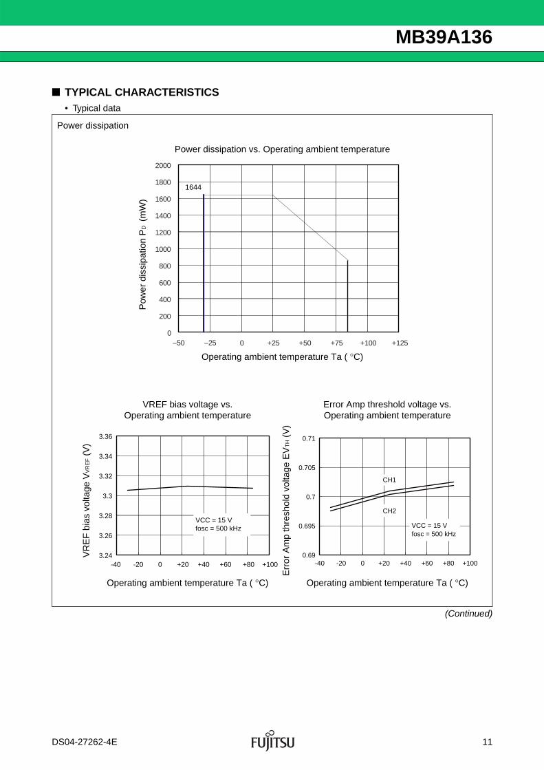
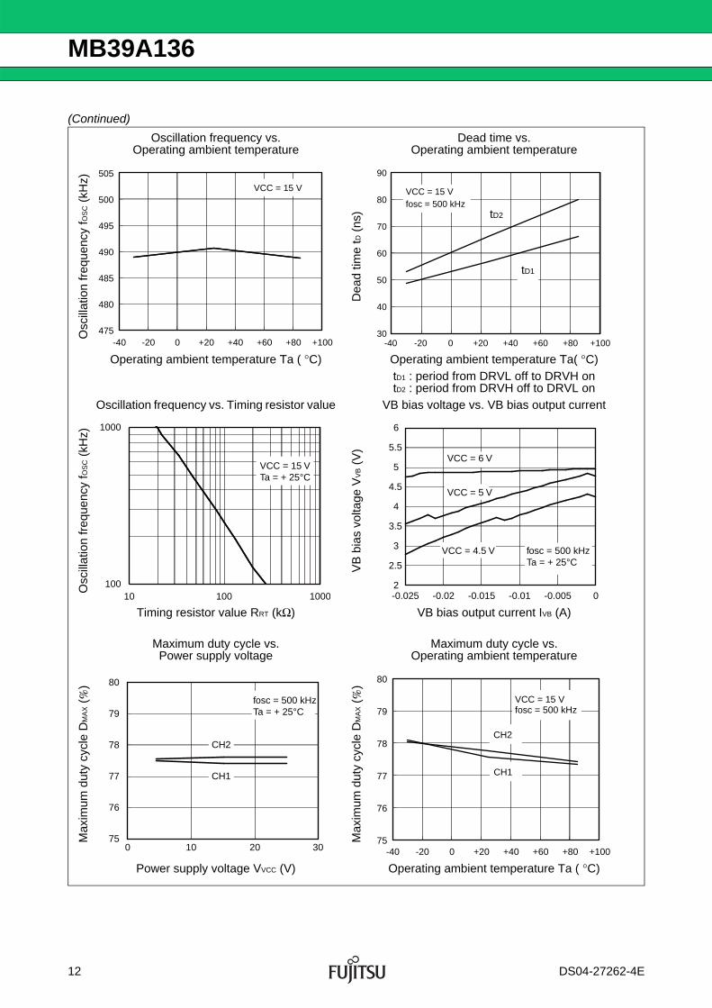
■ TYPICAL CHARACTERISTICS• Typical data
(Continued)
Power dissipation
Power dissipation vs. Operating ambient temperatureP
ower
dis
sipa
tion
PD
(m
W)
Operating ambient temperature Ta ( °C)
0
200
400
600
800
1000
1200
1400
1600
1800
2000
−50 −25 0 +25 +50 +75 +100 +125
1644
VREF bias voltage vs. Operating ambient temperature
Error Amp threshold voltage vs. Operating ambient temperature
VR
EF
bia
s vo
ltage
VV
RE
F (
V)
Err
or A
mp
thre
shol
d vo
ltage
EV
TH (
V)
Operating ambient temperature Ta ( °C) Operating ambient temperature Ta ( °C)
3.24
3.26
3.28
3.3
3.32
3.34
3.36
-40 -20 0 +20 +40 +60 +80 +100
VCC = 15 Vfosc = 500 kHz
-40 -20 0 +20 +40 +60 +80 +1000.69
0.695
0.7
0.705
0.71
CH1
CH2
VCC = 15 Vfosc = 500 kHz
DS04-27262-4E 11
MB39A136
(Continued)
Oscillation frequency vs.Operating ambient temperature
Dead time vs.Operating ambient temperature
Osc
illat
ion
freq
uenc
y fO
SC (
kHz)
Dea
d tim
e tD
(ns
)Operating ambient temperature Ta ( °C) Operating ambient temperature Ta( °C)
tD1 : period from DRVL off to DRVH ontD2 : period from DRVH off to DRVL on
Oscillation frequency vs. Timing resistor value VB bias voltage vs. VB bias output current
Osc
illat
ion
freq
uenc
y fO
SC (
kHz)
VB
bia
s vo
ltage
VV
B (
V)
Timing resistor value RRT (kΩ) VB bias output current IVB (A)
Maximum duty cycle vs. Power supply voltage
Maximum duty cycle vs. Operating ambient temperature
Max
imum
dut
y cy
cle
DM
AX (
%)
Max
imum
dut
y cy
cle
DM
AX (
%)
Power supply voltage VVCC (V) Operating ambient temperature Ta ( °C)
-40 -20 0 +20 +40 +60 +80 +100475
480
485
490
495
500
505
VCC = 15 V
-40 -20 0 +20 +40 +60 +80 +10030
40
50
60
70
80
90
VCC = 15 Vfosc = 500 kHz
tD2
tD1
VCC = 15 VTa = + 25°C
1000
10010 100 1000
fosc = 500 kHzTa = + 25°C
-0.025 -0.02
VCC = 6 V
VCC = 5 V
VCC = 4.5 V
-0.01-0.015 -0.005 0
5.5
6
5
4.5
4
3.5
3
2.5
2
fosc = 500 kHzTa = + 25°C
CH2
CH1
80
79
78
77
76
750 10 20 30 -40 -20 0 +20 +40 +60 +80 +100
75
76
77
78
79
80
VCC = 15 Vfosc = 500 kHz
CH2
CH1
12 DS04-27262-4E
MB39A136
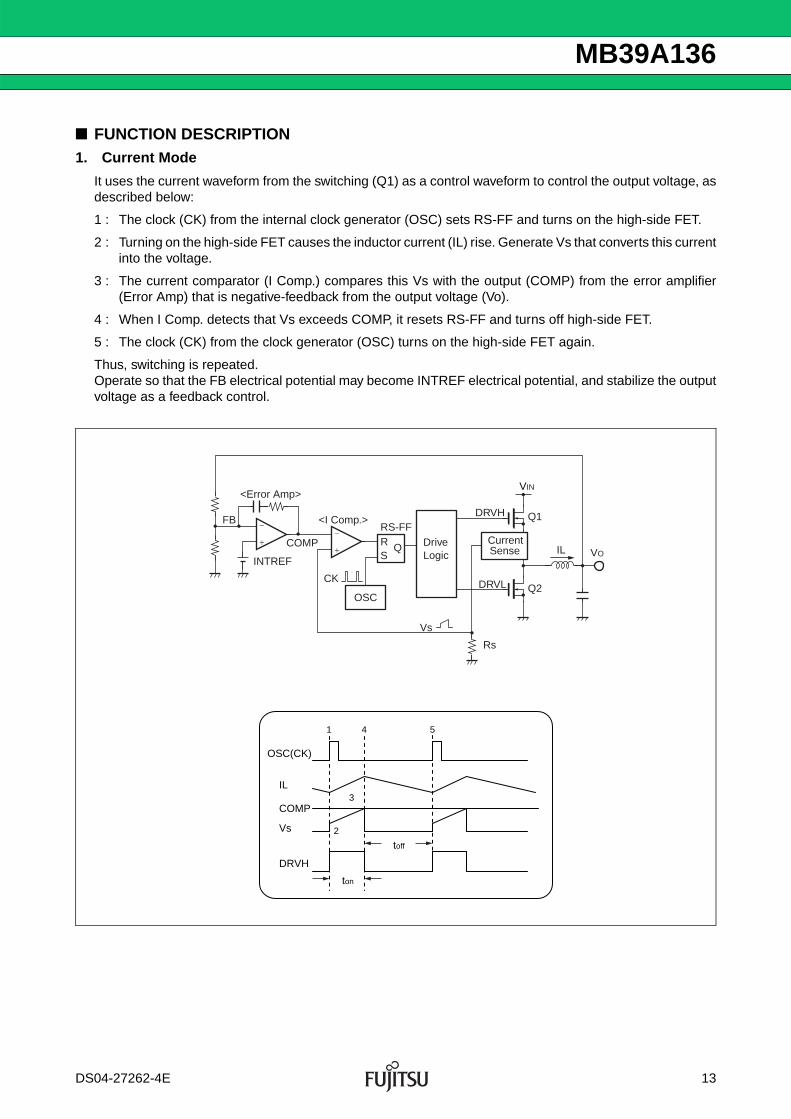
■ FUNCTION DESCRIPTION1. Current Mode
It uses the current waveform from the switching (Q1) as a control waveform to control the output voltage, asdescribed below:
1 : The clock (CK) from the internal clock generator (OSC) sets RS-FF and turns on the high-side FET.
2 : Turning on the high-side FET causes the inductor current (IL) rise. Generate Vs that converts this currentinto the voltage.
3 : The current comparator (I Comp.) compares this Vs with the output (COMP) from the error amplifier(Error Amp) that is negative-feedback from the output voltage (Vo).
4 : When I Comp. detects that Vs exceeds COMP, it resets RS-FF and turns off high-side FET.
5 : The clock (CK) from the clock generator (OSC) turns on the high-side FET again.
Thus, switching is repeated. Operate so that the FB electrical potential may become INTREF electrical potential, and stabilize the outputvoltage as a feedback control.
INTREF
VIN
IL VO
Vs
FB
COMP
RS-FF<I Comp.>
Rs
<Error Amp>
CK
DRVH
DRVLOSC
DriveLogic
RS
QCurrentSense
−
+−
+
Q1
Q2
ton
COMP
toff
Vs
IL
OSC(CK)
DRVH
1
2
3
4 5
DS04-27262-4E 13
MB39A136
(1) Reference Voltage Block (REF)
The reference voltage circuit (REF) generates a temperature-compensated reference voltage (3.3 [V] Typ)using the voltage supplied from the VCC pin. The voltage is used as the reference voltage for the IC's internalcircuit. The reference voltage can be used to supply a load current of up to 100 μA to an external devicethrough the VREF pin.
(2) Bias Voltage Block (VB Reg.)
Bias Voltage Block (VB Reg.) generates the reference voltage used for IC’s internal circuit, using the voltagesupplied from the VCC pin. The reference voltage is a temperature-compensated stable voltage (5 [V] Typ)to supply a current of up to 100 mA through the VB pin.
(3) Under Voltage Lockout Protection Circuit Block (UVLO)
The circuit protects against IC malfunction and system destruction/deterioration in a transitional state or amomentary drop when a bias voltage (VB) or an internal reference voltage (VREF) starts. It detects a voltagedrop at the VB pin or the VREF pin and stops IC operation. When voltages at the VB pin and the VREF pinexceed the threshold voltage of the under voltage lockout protection circuit, the system is restored.
(4) Soft-start/Soft-stop Block (Soft-Start, Soft-Stop)
Soft-start
It protects a rush current or an output voltage (VOx) from overshooting at the output start. Since the lampvoltage generated by charging the capacitor connecting to the CSx pin is used for the reference voltage ofthe error amplifier (Error Amp), it can set the soft-start time independent of a load of the output (VOx). Whenthe IC starts with “H” level of the CTLx pin, the capacitor at the CSx pin (CS) starts to be charged at 5.5 μA.The output voltage (VOx) during the soft-start period rises in proportion to the voltage at the CSx pin generatedby charging the capacitor at the CSx pin.
During the soft-start with 0.8 V > voltage at CS1 and CS2 pins, operations are as follows:• Fixed PWM operation only (fixed PWM even if MODE pin is set to “L”)• Over-voltage protection function and under-voltage protection function are invalid.
Soft-stop
It discharges electrical charges stored in a smoothing capacitor at output stop. Setting the CTLx pin to “L”level starts the soft-stop function independent of a load of output (Vox). Since the capacitor connecting tothe CSx pin starts to discharge through the IC-built-in soft-stop discharging resistance (70 [kΩ] Typ) whenthe CTLx pin sets at “L” level enters its lamp voltage into the error amplifier (Error Amp), the soft-stop timecan be set independent of a load of output (VOx). When discharging causes the voltage at the CSx pin todrop below 100 mV (Typ), the IC shuts down and changes to the stand-by state. In addition, the soft-stopfunction operates after the under-voltage protection circuit block (UVP Comp.) is latched or after the over-temperature protection circuit block (OTP) detects over-temperature.
During the soft-stop with, 0.8 V > voltage at CS1 and CS2 pins, operations are as follows:• Fixed PWM operation only (fixed PWM even if MODE pin is set to “L”)• Over-voltage protection function and under-voltage protection function are invalid.
(5) Clock Generator Block (OSC)
The clock generator has the built-in oscillation frequency setting capacitor and generates a clock that180°phase shifted from each channel by connecting the oscillation frequency setting resistor to the RT pin(Symmetrical-Phase method).
14 DS04-27262-4E
MB39A136
(6-1) Error Amp Block (Error Amp1, Error Amp2)
The error amplifiers (Error Amp1 and Error Amp2) detect the output voltage from the DC/DC converter andoutput to the current comparators (I Comp.1 and I Comp.2). The output voltage setting resistor externallyconnected to FB1 and FB2 pins allows an arbitrary output voltage to be set.
In addition, since an external resistor and an external capacitor serially connected between COMP1 andFB1 pins and between COMP2 and FB2 pins allow an arbitrary loop gain to be set, it is possible for thesystem to compensate a phase stably.
(6-2) Over Current Detection (Protection) Block (ILIM)
It is the current detection circuit to restrict an output current (IOX). The over current detection block (ILIM)compares an output waveform of the level converter of each channel (see “(12) Level Converter Block(LVCNV)”) with the ILIMx pin voltage in every cycle. As a load resistance (ROX) drops, a load current (IOX)increases. Therefore, the output waveform of the level converter exceeds the ILIM pin voltage of each channel.At this time, the output current can be restricted by turning off FET on the high-side and suppressing a peakvalue of the inductor current.
As a result, the output voltage (VOX) should drop.
Furthermore, if the output voltage drops and the electrical potential at the FBx pin drops below 0.3 V, theoscillation frequency (fOSC) drops to 1/8.
(7) Over-voltage Protection Circuit Block (OVP Comp.)
The circuit protects a device connecting to the output when the output voltage (VOx) rises.
It compares 1.15 times (Typ) of the internal reference voltage (INTREF) (0.7 V) that is non-inverting-enteredinto the error amplifier with the feedback voltage that is inverting-entered into the error amplifier and if itdetects the state where the latter is higher than the former by 50 μs (Typ). It stops the voltage output bysetting the RS latch, setting the DRVHx pin to “L” level, setting the DRVLx pin to “H” level, turning off thehigh-side FETs, and turning on the low-side FETs.
The conditions below cancel the protection function:• Setting CTL1 and CTL2 to “L”.• Setting the power supply voltage below the UVLO threshold voltage (VTHL1 and VTHL2).
(8) Under-voltage Protection Circuit Block (UVP Comp.)
It protects a device connecting to the output by stopping the output when the output voltage (VOX) drops.
It compares 0.7 times (Typ) of the internal reference voltage (INTREF) (0.7 V) that is non-inverting-enteredinto the error amplifier with the feedback voltage that is inverting-entered into the error amplifier and if itdetects the state where the latter is lower than the former by 512/fosc [s](Typ), it stops the voltage output forboth channels by setting the RS latch.
The conditions below cancel the protection function:• Setting CTL1 and CTL2 to “L”.• Setting the power supply voltage below the UVLO threshold voltage (VTHL1 and VTHL2).
(9) Over temperature Protection Circuit Block (OTP)
The circuit protects an IC from heat-destruction. If the temperature at the joint part reaches +160 °C, thecircuit stops the voltage output for both channels by discharging the capacitor connecting to the CSx pinthrough the soft-stop discharging resistance (70 [kΩ] Typ) in the IC. In addition, if the temperature at the joint part drops to +135 °C, the output restarts again through the soft-start function. Make sure to design the DC/DC power supply system so that the over temperature protection does not startfrequently.
DS04-27262-4E 15
MB39A136
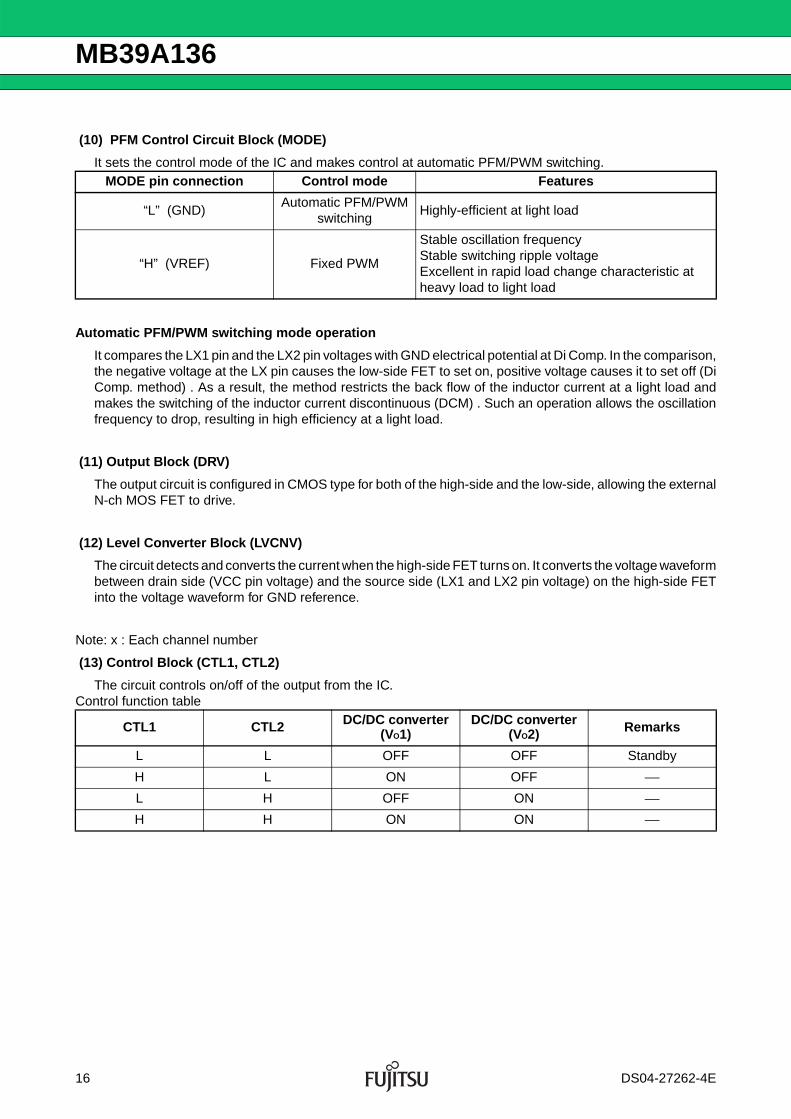
(10) PFM Control Circuit Block (MODE)
It sets the control mode of the IC and makes control at automatic PFM/PWM switching.
Automatic PFM/PWM switching mode operation
It compares the LX1 pin and the LX2 pin voltages with GND electrical potential at Di Comp. In the comparison,the negative voltage at the LX pin causes the low-side FET to set on, positive voltage causes it to set off (DiComp. method) . As a result, the method restricts the back flow of the inductor current at a light load andmakes the switching of the inductor current discontinuous (DCM) . Such an operation allows the oscillationfrequency to drop, resulting in high efficiency at a light load.
(11) Output Block (DRV)
The output circuit is configured in CMOS type for both of the high-side and the low-side, allowing the externalN-ch MOS FET to drive.
(12) Level Converter Block (LVCNV)
The circuit detects and converts the current when the high-side FET turns on. It converts the voltage waveformbetween drain side (VCC pin voltage) and the source side (LX1 and LX2 pin voltage) on the high-side FETinto the voltage waveform for GND reference.
Note: x : Each channel number
(13) Control Block (CTL1, CTL2)
The circuit controls on/off of the output from the IC.Control function table
MODE pin connection Control mode Features
“L” (GND) Automatic PFM/PWM
switchingHighly-efficient at light load
“H” (VREF) Fixed PWM
Stable oscillation frequencyStable switching ripple voltageExcellent in rapid load change characteristic at heavy load to light load
CTL1 CTL2 DC/DC converter (VO1)
DC/DC converter (VO2) Remarks
L L OFF OFF Standby
H L ON OFF ⎯L H OFF ON ⎯H H ON ON ⎯
16 DS04-27262-4E
MB39A136
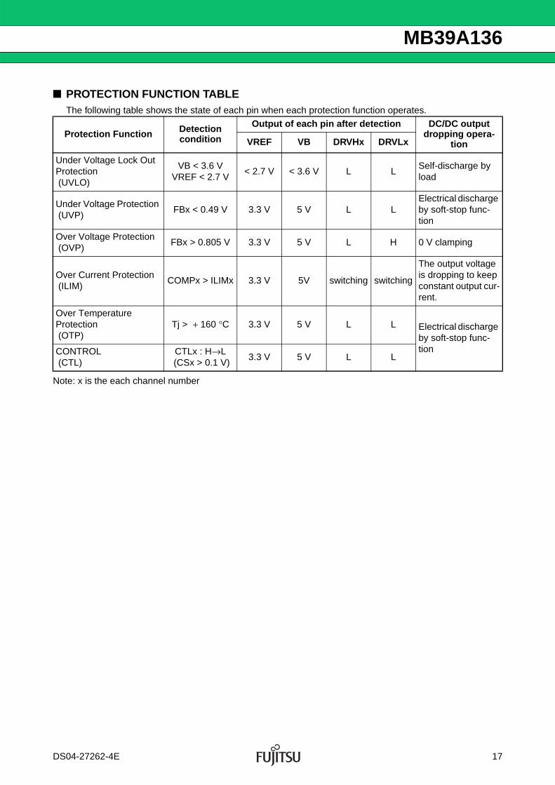
■ PROTECTION FUNCTION TABLEThe following table shows the state of each pin when each protection function operates.
Note: x is the each channel number
Protection Function Detection condition
Output of each pin after detection DC/DC output dropping opera-
tionVREF VB DRVHx DRVLx
Under Voltage Lock Out Protection (UVLO)
VB < 3.6 VVREF < 2.7 V
< 2.7 V < 3.6 V L LSelf-discharge by load
Under Voltage Protection (UVP)
FBx < 0.49 V 3.3 V 5 V L LElectrical discharge by soft-stop func-tion
Over Voltage Protection (OVP)
FBx > 0.805 V 3.3 V 5 V L H 0 V clamping
Over Current Protection (ILIM)
COMPx > ILIMx 3.3 V 5V switching switching
The output voltage is dropping to keep constant output cur-rent.
Over Temperature Protection (OTP)
Tj > + 160 °C 3.3 V 5 V L L Electrical discharge by soft-stop func-tionCONTROL
(CTL) CTLx : H→L
(CSx > 0.1 V) 3.3 V 5 V L L
DS04-27262-4E 17
MB39A136
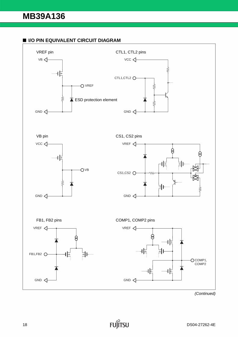
■ I/O PIN EQUIVALENT CIRCUIT DIAGRAM
(Continued)
VCC
GND
VB
VREF
VB
GND
VCC
GND
CTL1,CTL2
VREF
GND
CS1,CS2
VREF
GND
FB1,FB2
VREF
GND
COMP1,COMP2
VB pin CS1, CS2 pins
VREF pin CTL1, CTL2 pins
FB1, FB2 pins COMP1, COMP2 pins
ESD protection element
18 DS04-27262-4E
MB39A136
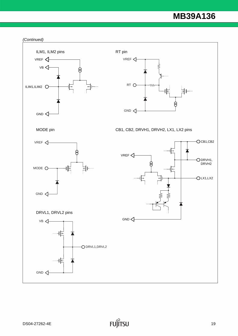
(Continued)
DRVL1,DRVL2
VREF
GND
RT
VREF
GND
LX1,LX2
CB1,CB2
DRVH1,DRVH2
VB
GND
ILIM1,ILIM2
VREF
GND
MODE
VREF
GND
ILIM1,ILIM2
VREF
GND
VB
VREF
GND
LX1,LX2
CB1,CB2
DRVH1, DRVH2
MODE pin CB1, CB2, DRVH1, DRVH2, LX1, LX2 pins
ILM1, ILM2 pins RT pin
DRVL1, DRVL2 pins
DS04-27262-4E 19
MB39A136
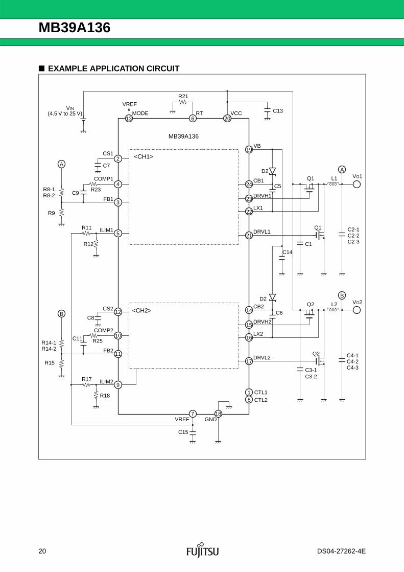
■ EXAMPLE APPLICATION CIRCUIT
VCCVIN
(4.5 V to 25 V) MODE
VREF
R21
C13
3
20
FB1
4COMP1
2CS1
A
613
C7
R23C9
R8-1R8-2
R9
MB39A136
<CH1>
5ILIM1R11
R12
11
10
12CS2
COMP2
FB2
<CH2>
9ILIM2
C8
C11 R25R14-1R14-2
R15
R17
R18
7 18GNDVREF
C15
1
15
16
14
17
CB2
DRVH2
DRVL2
LX2
VO2
CTL1CTL28
D2Q2 L2
Q2 C4-1C4-2C4-3C3-1
C3-2
C6
B
23
22
24
21
CB1
DRVH1
DRVL1
LX1
19VB
VO1AD2
Q1 L1
Q1 C2-1C2-2C2-3C1
C5
C14
RT
B
20 DS04-27262-4E
MB39A136
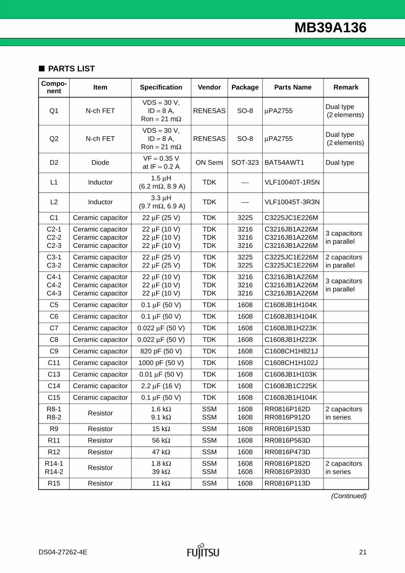
■ PARTS LIST
(Continued)
Compo-nent Item Specification Vendor Package Parts Name Remark
Q1 N-ch FETVDS = 30 V,
ID = 8 A, Ron = 21 mΩ
RENESAS SO-8 μPA2755Dual type (2 elements)
Q2 N-ch FETVDS = 30 V,
ID = 8 A, Ron = 21 mΩ
RENESAS SO-8 μPA2755Dual type (2 elements)
D2 DiodeVF = 0.35 Vat IF = 0.2 A
ON Semi SOT-323 BAT54AWT1 Dual type
L1 Inductor1.5 μH
(6.2 mΩ, 8.9 A) TDK ⎯ VLF10040T-1R5N
L2 Inductor3.3 μH
(9.7 mΩ, 6.9 A) TDK ⎯ VLF10045T-3R3N
C1 Ceramic capacitor 22 μF (25 V) TDK 3225 C3225JC1E226M
C2-1 C2-2 C2-3
Ceramic capacitor Ceramic capacitor Ceramic capacitor
22 μF (10 V) 22 μF (10 V) 22 μF (10 V)
TDK TDK TDK
3216 3216 3216
C3216JB1A226M C3216JB1A226M C3216JB1A226M
3 capacitors in parallel
C3-1 C3-2
Ceramic capacitor Ceramic capacitor
22 μF (25 V) 22 μF (25 V)
TDK TDK
3225 3225
C3225JC1E226M C3225JC1E226M
2 capacitors in parallel
C4-1 C4-2 C4-3
Ceramic capacitor Ceramic capacitor Ceramic capacitor
22 μF (10 V) 22 μF (10 V) 22 μF (10 V)
TDK TDK TDK
3216 3216 3216
C3216JB1A226M C3216JB1A226M C3216JB1A226M
3 capacitors in parallel
C5 Ceramic capacitor 0.1 μF (50 V) TDK 1608 C1608JB1H104K
C6 Ceramic capacitor 0.1 μF (50 V) TDK 1608 C1608JB1H104K
C7 Ceramic capacitor 0.022 μF (50 V) TDK 1608 C1608JB1H223K
C8 Ceramic capacitor 0.022 μF (50 V) TDK 1608 C1608JB1H223K
C9 Ceramic capacitor 820 pF (50 V) TDK 1608 C1608CH1H821J
C11 Ceramic capacitor 1000 pF (50 V) TDK 1608 C1608CH1H102J
C13 Ceramic capacitor 0.01 μF (50 V) TDK 1608 C1608JB1H103K
C14 Ceramic capacitor 2.2 μF (16 V) TDK 1608 C1608JB1C225K
C15 Ceramic capacitor 0.1 μF (50 V) TDK 1608 C1608JB1H104K
R8-1 R8-2
Resistor1.6 kΩ 9.1 kΩ
SSMSSM
1608 1608
RR0816P162DRR0816P912D
2 capacitors in series
R9 Resistor 15 kΩ SSM 1608 RR0816P153D
R11 Resistor 56 kΩ SSM 1608 RR0816P563D
R12 Resistor 47 kΩ SSM 1608 RR0816P473D
R14-1R14-2
Resistor1.8 kΩ39 kΩ
SSMSSM
16081608
RR0816P182DRR0816P393D
2 capacitors in series
R15 Resistor 11 kΩ SSM 1608 RR0816P113D
DS04-27262-4E 21
MB39A136
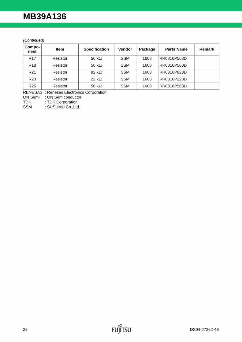
(Continued)
RENESAS : Renesas Electronics CorporationON Semi : ON SemiconductorTDK : TDK CorporationSSM : SUSUMU Co.,Ltd.
Compo-nent Item Specification Vendor Package Parts Name Remark
R17 Resistor 56 kΩ SSM 1608 RR0816P563D
R18 Resistor 56 kΩ SSM 1608 RR0816P563D
R21 Resistor 82 kΩ SSM 1608 RR0816P823D
R23 Resistor 22 kΩ SSM 1608 RR0816P223D
R25 Resistor 56 kΩ SSM 1608 RR0816P563D
22 DS04-27262-4E
MB39A136
■ APPLICATION NOTESetting method for PFM/PWM and fixed PWM modes
For the setting method for each mode, see“■ FUNCTION DESCRIPTION (10) PFM Control Circuit Block (MODE)”.
Cautions at PFM/PWM mode
If a load current drops rapidly because of rapid load change and others, it tends to take a lot of time to restoreovershooting of an output voltage.
As a result, the over-voltage protection may operate.
In this case, solution are possible by the addition of the load resistance of value to be able to restore theoutput voltage in the over-voltage detection time.
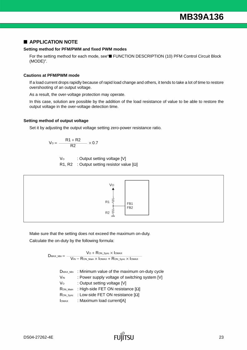
Setting method of output voltage
Set it by adjusting the output voltage setting zero-power resistance ratio.
Make sure that the setting does not exceed the maximum on-duty.
Calculate the on-duty by the following formula:
VO = R1 + R2
× 0.7R2
VO : Output setting voltage [V]R1, R2 : Output setting resistor value [Ω]
DMAX_Min = VO + RON_Sync × IOMAX
VIN − RON_Main × IOMAX + RON_Sync × IOMAX
DMAX_Min : Minimum value of the maximum on-duty cycleVIN : Power supply voltage of switching system [V]VO : Output setting voltage [V]RON_Main : High-side FET ON resistance [Ω]RON_Sync : Low-side FET ON resistance [Ω]IOMAX : Maximum load current[A]
R1
VO
R2
FB1FB2
DS04-27262-4E 23
MB39A136
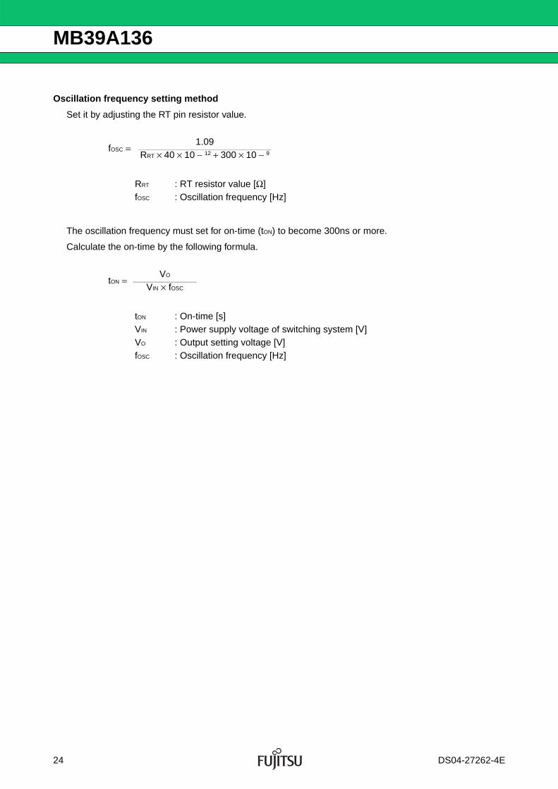
Oscillation frequency setting method
Set it by adjusting the RT pin resistor value.
The oscillation frequency must set for on-time (tON) to become 300ns or more.
Calculate the on-time by the following formula.
fOSC = 1.09
RRT × 40 × 10 − 12 + 300 × 10 − 9
RRT : RT resistor value [Ω]fOSC : Oscillation frequency [Hz]
tON = VO
VIN × fOSC
tON : On-time [s]VIN : Power supply voltage of switching system [V]VO : Output setting voltage [V]fOSC : Oscillation frequency [Hz]
24 DS04-27262-4E
MB39A136
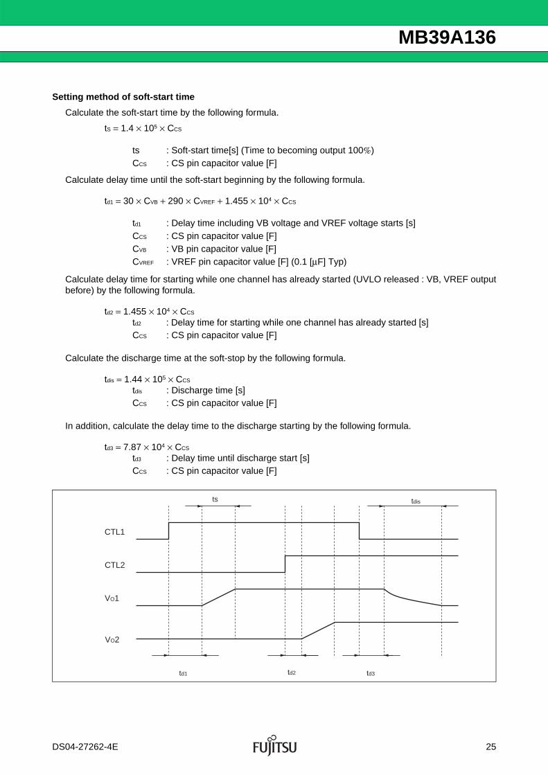
Setting method of soft-start time
Calculate the soft-start time by the following formula.
tS = 1.4 × 10⁵ × CCS
Calculate delay time until the soft-start beginning by the following formula.
td1 = 30 × CVB + 290 × CVREF + 1.455 × 10⁴ × CCS
Calculate delay time for starting while one channel has already started (UVLO released : VB, VREF outputbefore) by the following formula.
td2 = 1.455 × 10⁴ × CCS
Calculate the discharge time at the soft-stop by the following formula.
tdis = 1.44 × 10⁵ × CCS
In addition, calculate the delay time to the discharge starting by the following formula.
td3 = 7.87 × 10⁴ × CCS
ts : Soft-start time[s] (Time to becoming output 100%)CCS : CS pin capacitor value [F]
td1 : Delay time including VB voltage and VREF voltage starts [s]CCS : CS pin capacitor value [F]CVB : VB pin capacitor value [F]CVREF : VREF pin capacitor value [F] (0.1 [μF] Typ)
td2 : Delay time for starting while one channel has already started [s]CCS : CS pin capacitor value [F]
tdis : Discharge time [s]CCS : CS pin capacitor value [F]
td3 : Delay time until discharge start [s]CCS : CS pin capacitor value [F]
CTL1
CTL2
VO1
VO2
ts
td1 td2
tdis
td3
DS04-27262-4E 25
MB39A136
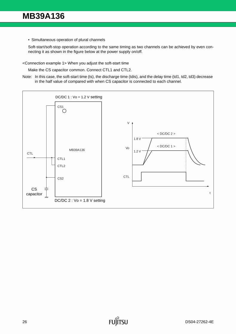
• Simultaneous operation of plural channels
Soft-start/soft-stop operation according to the same timing as two channels can be achieved by even con-necting it as shown in the figure below at the power supply on/off.
<Connection example 1> When you adjust the soft-start time
Make the CS capacitor common. Connect CTL1 and CTL2.
Note: In this case, the soft-start time (ts), the discharge time (tdis), and the delay time (td1, td2, td3) decrease in the half value of compared with when CS capacitor is connected to each channel.
CS1
CTL1
MB39A136
CS2
CTL
V
t
< DC/DC 2 >
< DC/DC 1 >
1.8 V
1.2 V
CTL2
Vo
CTL
DC/DC 2 : Vo = 1.8 V setting
DC/DC 1 : Vo = 1.2 V setting
CS capacitor
26 DS04-27262-4E
MB39A136
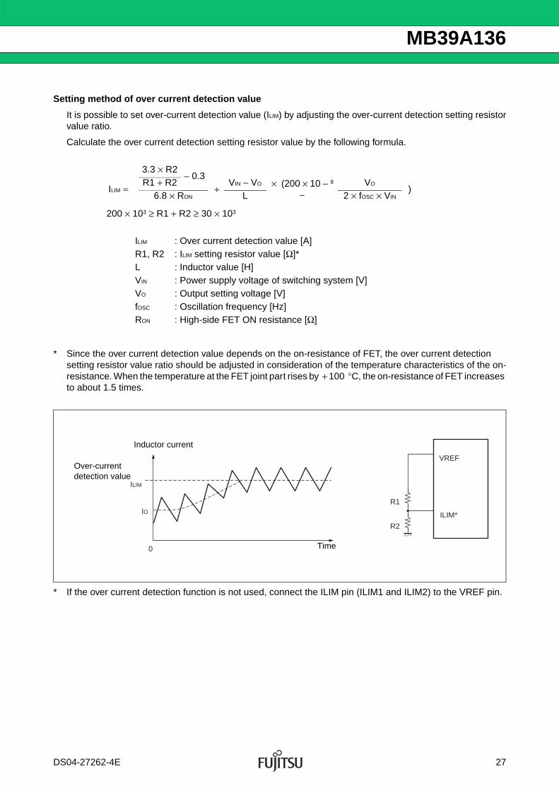
Setting method of over current detection value
It is possible to set over-current detection value (ILIM) by adjusting the over-current detection setting resistorvalue ratio.
Calculate the over current detection setting resistor value by the following formula.
200 × 103 ≥ R1 + R2 ≥ 30 × 103
* Since the over current detection value depends on the on-resistance of FET, the over current detection setting resistor value ratio should be adjusted in consideration of the temperature characteristics of the on-resistance. When the temperature at the FET joint part rises by + 100 °C, the on-resistance of FET increases to about 1.5 times.
* If the over current detection function is not used, connect the ILIM pin (ILIM1 and ILIM2) to the VREF pin.
3.3 × R2− 0.3
ILIM = R1 + R2
+ VIN − VO × (200 × 10 − 9
− VO
) 6.8 × RON L 2 × fOSC × VIN
ILIM : Over current detection value [A]R1, R2 : ILIM setting resistor value [Ω]*L : Inductor value [H]VIN : Power supply voltage of switching system [V]VO : Output setting voltage [V]fOSC : Oscillation frequency [Hz]RON : High-side FET ON resistance [Ω]
VREF
ILIM*
R1
R2
IO
ILIM
0
Inductor current
Time
Over-current detection value
DS04-27262-4E 27
MB39A136
Selection of smoothing inductor
The inductor value selects the value that the ripple current peak-to-peak value becomes 50% or less of themaximum load current as a rough standard. Calculate the inductor value in this case by the following formula.
An inductor ripple current value limited on the principle of operation is necessary for this device. However,when it uses the high-side FET of the low Ron resistance, the switching ripple voltage become small, andthe inductor ripple current value may become insufficient. This should be solved by the oscillation frequencyor reducing the inductor value. Select the one of the inductor value that meets a requirement listed below.
It is necessary to calculate the maximum current value that flows to the inductor to judge whether the electriccurrent that flows to the inductor is a rated value or less. Calculate the maximum current value of the inductorby the following formula.
L ≥ VIN − VO
× VO
LOR × IOMAX VIN × fOSC
L : Inductor value [H]IOMAX : Maximum load current [A]LOR : Ripple current peak-to-peak value of Maximum load current ratio (=0.5)VIN : Power supply voltage of switching system [V]VO : Output setting voltage [V]fOSC : Oscillation frequency [Hz]
L ≤ VIN − VO
× VO
× RONΔVRON VIN × fOSC
L : Inductor value [H]VIN : Power supply voltage of switching system [V]VO : Output setting voltage [V]fOSC : Oscillation frequency [Hz]ΔVRON : Ripple voltage [V] (20 mV or more is recommended) RON : High-side FET ON resistance [Ω]
ILMAX ≥ IoMAX + ΔIL
, ΔIL = VIN − VO
× VO
2 L VIN × fOSC
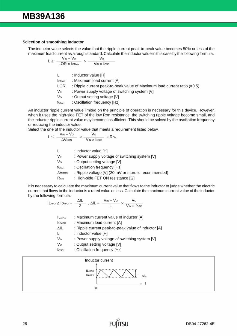
ILMAX : Maximum current value of inductor [A]IoMAX : Maximum load current [A]ΔIL : Ripple current peak-to-peak value of inductor [A]L : Inductor value [H]VIN : Power supply voltage of switching system [V]VO : Output setting voltage [V]fOSC : Oscillation frequency [Hz]
ΔILIoMAX
ILMAX
0
Inductor current
t
28 DS04-27262-4E
MB39A136
Selection of SWFET
The switching ripple voltage generated between drain and sources on high-side FET is necessary for thisdevice operation. Select the one of the SWFET of on-resistance that satisfies the following formula.
Select FET ratings with a margin enough for the input voltage and the load current. Ratings with the over-current detection setting value or more are recommended.
Calculate a necessary rated value of high-side FET and low-side FET by the following formula.
VDS > VIN
VGS > VB
Moreover, it is necessary to calculate the loss of SWFET to judge whether a permissible loss of SWFET isa rated value or less. Calculate the loss on high-side FET by the following formula.
PMainFET = PRON_Main + PSW_Main
RON_Main ≥ ΔVRON_Main
, RON_Main ≤ VRONMAX
ΔILILIM +
ΔIL2
RON_Main : High-side FET ON resistance [Ω]ΔIL : Ripple current peak-to-peak value of inductor [A]ΔVRON_Main : High-side FET ripple voltage [V] (20mV or more is recommended)ILIM : Over current detection value [A]VRONMAX : Maximum current sense voltage [V] (240mV or less is recommended)
ID > IoMAX + ΔIL2
ID : Rated drain current [A]IoMAX : Maximum load current [A]ΔIL : Ripple current peak-to-peak value of inductor [A]
VDS : Rated voltage between drain and source [V]VIN : Power supply voltage of switching system [V]
VGS : Rated voltage between gate and source [V]VB : VB voltage [V]
PMainFET : High-side FET loss [W]PRON_Main : High-side FET conduction loss [W]PSW_Main : High-side FET SW loss [W]
DS04-27262-4E 29
MB39A136
High-side FET conduction loss
High-side FET SW loss
Calculate the Ibtm, the Itop, the tr and the tf simply by the following formula.
PRON_Main = IoMAX2 × VO
× RON_MainVIN
PRON_Main : High-side FET conduction loss [W]IOMAX : Maximum load current [A]VIN : Power supply voltage of switching system [V]VO : Output voltage [V]RON_Main : High-side FET ON resistance [Ω]
PSW_Main = VIN × fOSC × (Ibtm × tr + Itop × tf)
2
PSW_Main : High-side FET SW loss [W]VIN : Power supply voltage of switching system [V]fOSC : Oscillation frequency [Hz] Ibtm : Ripple current bottom value of inductor [A]Itop : Ripple current top value of inductor [A]tr : Turn-on time on high-side FET [s]tf : Turn-off time on high-side FET[s]
Ibtm = IOMAX − ΔIL2
Itop = IOMAX + ΔIL2
tr = Qgd × 4
tf = Qgd × 1
5 − Vgs (on) Vgs (on)
IOMAX : Maximum load current [A]ΔIL : Ripple current peak-to-peak value of inductor [A]Qgd : Quantity of charge between gate and drain on high-side FET [C] Vgs (on) : Voltage between gate and source in Qgd on high-side FET [V]
30 DS04-27262-4E
MB39A136
Calculate the loss on low-side FET by the following formula.
* : The transition voltage of the voltage between drain and source on low-side FET is generally small, and the switching loss is omitted here for the small one as it is possible to disregard it.
The gate drive power of SWFET is supplied by LDO in IC, therefore all SWFET allowable maximum totalcharge (QgTotalMax) of 2ch is determined by the following formula.
Selection of fly-back diode
When the conversion efficiency is valued, the improved property of the conversion efficiency is possible bythe addition of the fly-back diode. Thought it is usually unnecessary. The effect is achieved in the conditionwhere the oscillation frequency is high or output voltage is lower. Select schottky barrier diode (SBD) thatthe forward current is as small as possible. In this DC/DC control IC, the period for the electric current flowsto fly back diode is limited to synchronous rectification period (60 ns × 2) because of using the synchronousrectification method. Therefore, select the one that the electric current of fly back diode doesn't exceedratings of forward current surge peak (IFSM).Calculate the forward current surge peak ratings of fly backdiode by the following formula.
Calculate ratings of the fly-back diode by the following formula:
VR_Fly > VIN
PSyncFET = PRon_Sync* = IoMAX2 × (1 − VO
) × Ron_SyncVIN
PSyncFET : Low-side FET loss [W]PRon_Sync : Low-side FET conduction loss [W]IOMAX : Maximum load current [A]VIN : Power supply voltage of switching system [V]VO : Output voltage [V]Ron_Sync : Low-side FET on-resistance [Ω]
QgTotalMax ≤ 0.095fOSC
QgTotalMax : SWFET allowable maximum total charge [C]fOSC : Oscillation frequency [Hz]
IFSM ≥ IoMAX + ΔIL2
IFSM : Forward current surge peak ratings of fly back diode [A]IoMAX : Maximum load current [A]ΔIL : Ripple current peak-to-peak value of inductor [A]
VR_Fly : Reverse voltage of fly-back diode direct current [V]VIN : Power supply voltage of switching system [V]
DS04-27262-4E 31
MB39A136
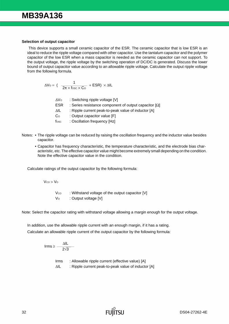
Selection of output capacitor
This device supports a small ceramic capacitor of the ESR. The ceramic capacitor that is low ESR is anideal to reduce the ripple voltage compared with other capacitor. Use the tantalum capacitor and the polymercapacitor of the low ESR when a mass capacitor is needed as the ceramic capacitor can not support. Tothe output voltage, the ripple voltage by the switching operation of DC/DC is generated. Discuss the lowerbound of output capacitor value according to an allowable ripple voltage. Calculate the output ripple voltagefrom the following formula.
Notes: • The ripple voltage can be reduced by raising the oscillation frequency and the inductor value besides capacitor.
• Capacitor has frequency characteristic, the temperature characteristic, and the electrode bias char-acteristic, etc. The effective capacitor value might become extremely small depending on the condition. Note the effective capacitor value in the condition.
Calculate ratings of the output capacitor by the following formula:
VCO > VO
Note: Select the capacitor rating with withstand voltage allowing a margin enough for the output voltage.
In addition, use the allowable ripple current with an enough margin, if it has a rating.
Calculate an allowable ripple current of the output capacitor by the following formula:
ΔVO = (1
+ ESR) × ΔIL2π × fOSC × CO
ΔVO : Switching ripple voltage [V]ESR : Series resistance component of output capacitor [Ω]ΔIL : Ripple current peak-to-peak value of inductor [A]CO : Output capacitor value [F]fOSC : Oscillation frequency [Hz]
VCO : Withstand voltage of the output capacitor [V]VO : Output voltage [V]
Irms ≥ ΔIL
2√3
Irms : Allowable ripple current (effective value) [A]ΔIL : Ripple current peak-to-peak value of inductor [A]
32 DS04-27262-4E
MB39A136
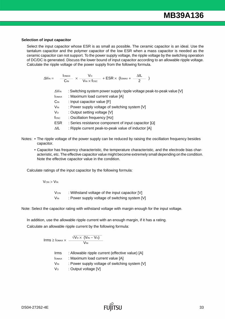
Selection of input capacitor
Select the input capacitor whose ESR is as small as possible. The ceramic capacitor is an ideal. Use thetantalum capacitor and the polymer capacitor of the low ESR when a mass capacitor is needed as theceramic capacitor can not support. To the power supply voltage, the ripple voltage by the switching operationof DC/DC is generated. Discuss the lower bound of input capacitor according to an allowable ripple voltage.Calculate the ripple voltage of the power supply from the following formula.
Notes: • The ripple voltage of the power supply can be reduced by raising the oscillation frequency besides capacitor.
• Capacitor has frequency characteristic, the temperature characteristic, and the electrode bias char-acteristic, etc. The effective capacitor value might become extremely small depending on the condition. Note the effective capacitor value in the condition.
Calculate ratings of the input capacitor by the following formula:
VCIN > VIN
Note: Select the capacitor rating with withstand voltage with margin enough for the input voltage.
In addition, use the allowable ripple current with an enough margin, if it has a rating.
Calculate an allowable ripple current by the following formula:
ΔVIN = IOMAX
× VO
+ ESR × (IOMAX + ΔIL
) CIN VIN × fOSC 2
ΔVIN : Switching system power supply ripple voltage peak-to-peak value [V]IOMAX : Maximum load current value [A]CIN : Input capacitor value [F]VIN : Power supply voltage of switching system [V]VO : Output setting voltage [V]fOSC : Oscillation frequency [Hz]ESR : Series resistance component of input capacitor [Ω]ΔIL : Ripple current peak-to-peak value of inductor [A]
VCIN : Withstand voltage of the input capacitor [V]VIN : Power supply voltage of switching system [V]
Irms ≥ IOMAX × √VO × (VIN − VO)
VIN
Irms : Allowable ripple current (effective value) [A]IOMAX : Maximum load current value [A]VIN : Power supply voltage of switching system [V]VO : Output voltage [V]
DS04-27262-4E 33
MB39A136
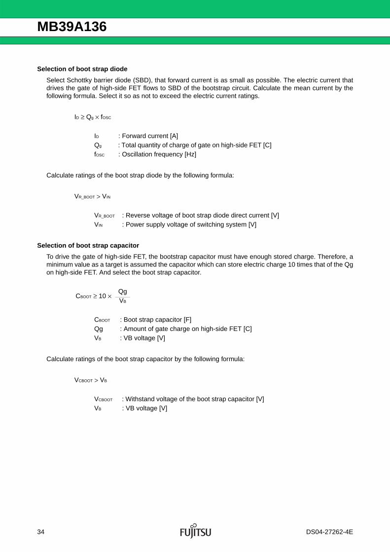
Selection of boot strap diode
Select Schottky barrier diode (SBD), that forward current is as small as possible. The electric current thatdrives the gate of high-side FET flows to SBD of the bootstrap circuit. Calculate the mean current by thefollowing formula. Select it so as not to exceed the electric current ratings.
ID ≥ Qg × fOSC
Calculate ratings of the boot strap diode by the following formula:
VR_BOOT > VIN
Selection of boot strap capacitor
To drive the gate of high-side FET, the bootstrap capacitor must have enough stored charge. Therefore, aminimum value as a target is assumed the capacitor which can store electric charge 10 times that of the Qgon high-side FET. And select the boot strap capacitor.
Calculate ratings of the boot strap capacitor by the following formula:
VCBOOT > VB
ID : Forward current [A]Qg : Total quantity of charge of gate on high-side FET [C]fOSC : Oscillation frequency [Hz]
VR_BOOT : Reverse voltage of boot strap diode direct current [V]VIN : Power supply voltage of switching system [V]
CBOOT ≥ 10 × QgVB
CBOOT : Boot strap capacitor [F]Qg : Amount of gate charge on high-side FET [C]VB : VB voltage [V]
VCBOOT : Withstand voltage of the boot strap capacitor [V]VB : VB voltage [V]
34 DS04-27262-4E
MB39A136
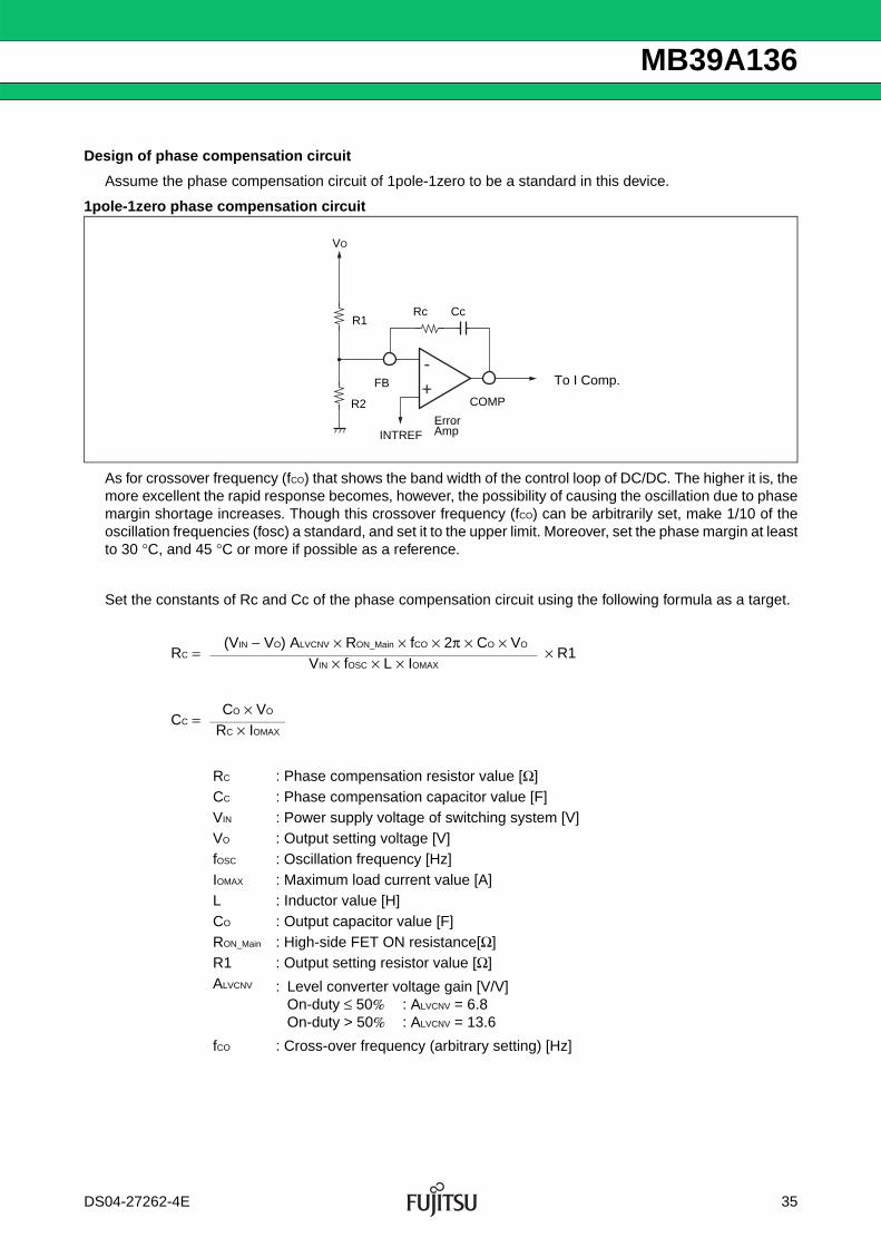
Design of phase compensation circuit
Assume the phase compensation circuit of 1pole-1zero to be a standard in this device.
1pole-1zero phase compensation circuit
As for crossover frequency (fCO) that shows the band width of the control loop of DC/DC. The higher it is, themore excellent the rapid response becomes, however, the possibility of causing the oscillation due to phasemargin shortage increases. Though this crossover frequency (fCO) can be arbitrarily set, make 1/10 of theoscillation frequencies (fosc) a standard, and set it to the upper limit. Moreover, set the phase margin at leastto 30 °C, and 45 °C or more if possible as a reference.
Set the constants of Rc and Cc of the phase compensation circuit using the following formula as a target.
RC = (VIN − VO) ALVCNV × RON_Main × fCO × 2π × CO × VO
× R1VIN × fOSC × L × IOMAX
CC = CO × VO
RC × IOMAX
RC : Phase compensation resistor value [Ω]CC : Phase compensation capacitor value [F]VIN : Power supply voltage of switching system [V]VO : Output setting voltage [V] fOSC : Oscillation frequency [Hz]IOMAX : Maximum load current value [A]L : Inductor value [H]CO : Output capacitor value [F]RON_Main : High-side FET ON resistance[Ω]R1 : Output setting resistor value [Ω]ALVCNV : Level converter voltage gain [V/V]
On-duty ≤ 50% : ALVCNV = 6.8On-duty > 50% : ALVCNV = 13.6
fCO : Cross-over frequency (arbitrary setting) [Hz]
INTREF
VO
COMP
R1
R2
Rc Cc
FB
ErrorAmp
-+
To I Comp.
DS04-27262-4E 35
MB39A136
VB pin capacitor
2.2 μF is assumed to be a standard, and when Qg of SWFET used is large, it is necessary to adjust it. Todrive the gate of high-side FET, the bootstrap capacitor must have enough stored charge. Therefore, aminimum value as a target is assumed the capacitor, which can store electric charge 100 times that of theQg of the SWFET. And select it.
Calculate ratings of the VB pin capacitor by the following formula:
VCVB > VB
CVB ≥ 100 × QgVB
CVB : VB pin capacitor value [F]
Qg : Total amount of gate charge of 2 ch respectively: high-side FET and low-side FET
[C]VB : VB voltage [V]
VCVB : Withstand voltage of the VB pin capacitor [V]VB : VB voltage [V]
36 DS04-27262-4E
MB39A136
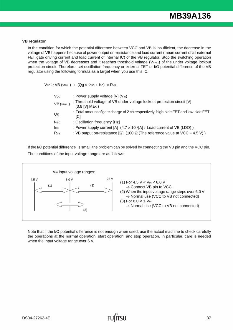
VB regulator
In the condition for which the potential difference between VCC and VB is insufficient, the decrease in thevoltage of VB happens because of power output on-resistance and load current (mean current of all externalFET gate driving current and load current of internal IC) of the VB regulator. Stop the switching operationwhen the voltage of VB decreases and it reaches threshold voltage (VTHL1) of the under voltage lockoutprotection circuit. Therefore, set oscillation frequency or external FET or I/O potential difference of the VBregulator using the following formula as a target when you use this IC.
VCC ≥ VB (VTHL1) + (Qg × fOSC + ICC) × RVB
If the I/O potential difference is small, the problem can be solved by connecting the VB pin and the VCC pin.
The conditions of the input voltage range are as follows:
Note that if the I/O potential difference is not enough when used, use the actual machine to check carefullythe operations at the normal operation, start operation, and stop operation. In particular, care is neededwhen the input voltage range over 6 V.
VCC : Power supply voltage [V] (VIN)
VB (VTHL1) : Threshold voltage of VB under-voltage lockout protection circuit [V]
(3.8 [V] Max )
Qg : Total amount of gate charge of 2 ch respectively: high-side FET and low-side FET
[C]fOSC : Oscillation frequency [Hz]ICC : Power supply current [A] (4.7 × 10⁻³[A] := Load current of VB (LDO) ) RVB : VB output on-resistance [Ω] (100 Ω (The reference value at VCC = 4.5 V) )
6.0 V4.5 V 25 V
(2)
(3)(1)(1) For 4.5 V < VIN < 6.0 V
→ Connect VB pin to VCC.(2) When the input voltage range steps over 6.0 V
→ Normal use (VCC to VB not connected) (3) For 6.0 V ≤ VIN
→ Normal use (VCC to VB not connected)
VIN input voltage ranges:
DS04-27262-4E 37
MB39A136
Power dissipation and the thermal design
As for this IC, considerations of the power dissipation and thermal design are not necessary in most casesbecause of its high efficiency. However, they are necessary for the use at the conditions of a high powersupply voltage, a high oscillation frequency, high load, and the high temperature.
Calculate IC internal loss (PIC) by the following formula.
PIC = VCC × (ICC + Qg × fOSC)
Calculate junction temperature (Tj) by the following formula.
Tj = Ta + θja × PIC
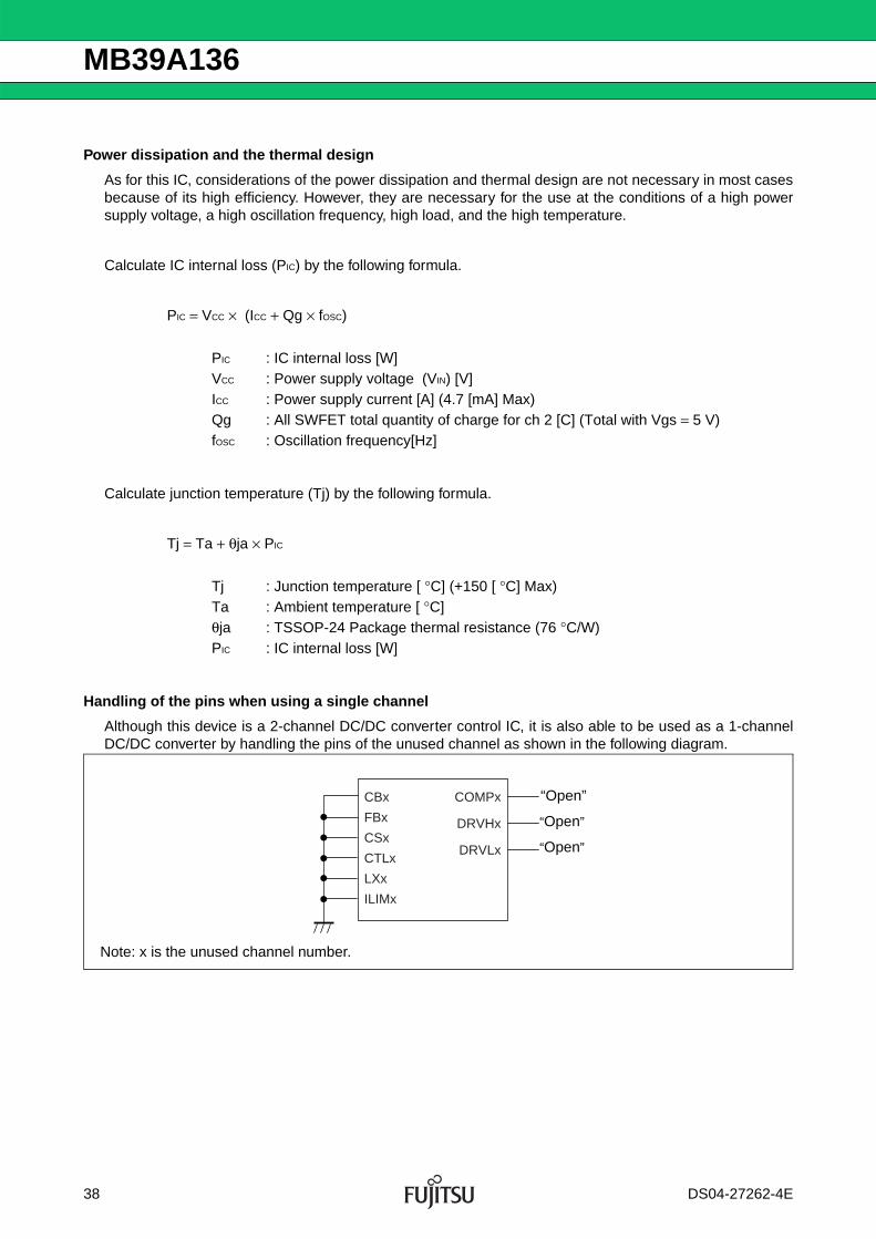
Handling of the pins when using a single channel
Although this device is a 2-channel DC/DC converter control IC, it is also able to be used as a 1-channelDC/DC converter by handling the pins of the unused channel as shown in the following diagram.
PIC : IC internal loss [W]VCC : Power supply voltage (VIN) [V]ICC : Power supply current [A] (4.7 [mA] Max) Qg : All SWFET total quantity of charge for ch 2 [C] (Total with Vgs = 5 V) fOSC : Oscillation frequency[Hz]
Tj : Junction temperature [ °C] (+150 [ °C] Max) Ta : Ambient temperature [ °C]θja : TSSOP-24 Package thermal resistance (76 °C/W) PIC : IC internal loss [W]
FBx
CBx
CSx
LXx
ILIMx
CTLx
DRVHx
COMPx
DRVLx
Note: x is the unused channel number.
“Open”
“Open”
“Open”
38 DS04-27262-4E
MB39A136
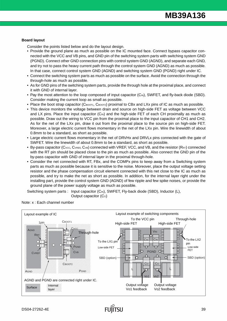
Board layout
Consider the points listed below and do the layout design.• Provide the ground plane as much as possible on the IC mounted face. Connect bypass capacitor con-
nected with the VCC and VB pins, and GND pin of the switching system parts with switching system GND(PGND). Connect other GND connection pins with control system GND (AGND), and separate each GND,and try not to pass the heavy current path through the control system GND (AGND) as much as possible.In that case, connect control system GND (AGND) and switching system GND (PGND) right under IC.
• Connect the switching system parts as much as possible on the surface. Avoid the connection through thethrough-hole as much as possible.
• As for GND pins of the switching system parts, provide the through hole at the proximal place, and connectit with GND of internal layer.
• Pay the most attention to the loop composed of input capacitor (CIN), SWFET, and fly-back diode (SBD).Consider making the current loop as small as possible.
• Place the boot strap capacitor (CBOOT1, CBOOT2) proximal to CBx and LXx pins of IC as much as possible. • This device monitors the voltage between drain and source on high-side FET as voltage between VCC
and LX pins. Place the input capacitor (CIN) and the high-side FET of each CH proximally as much aspossible. Draw out the wiring to VCC pin from the proximal place to the input capacitor of CH1 and CH2.As for the net of the LXx pin, draw it out from the proximal place to the source pin on high-side FET.Moreover, a large electric current flows momentary in the net of the LXx pin. Wire the linewidth of about0.8mm to be a standard, as short as possible.
• Large electric current flows momentary in the net of DRVHx and DRVLx pins connected with the gate ofSWFET. Wire the linewidth of about 0.8mm to be a standard, as short as possible.
• By-pass capacitor (CVCC, CVREF, CVB) connected with VREF, VCC, and VB, and the resistor (RRT) connectedwith the RT pin should be placed close to the pin as much as possible. Also connect the GND pin of theby-pass capacitor with GND of internal layer in the proximal through-hole.
• Consider the net connected with RT, FBx, and the COMPx pins to keep away from a Switching systemparts as much as possible because it is sensitive to the noise. Moreover, place the output voltage settingresistor and the phase compensation circuit element connected with this net close to the IC as much aspossible, and try to make the net as short as possible. In addition, for the internal layer right under theinstalling part, provide the control system GND (AGND) of few ripple and few spike noises, or provide theground plane of the power supply voltage as much as possible.
Switching system parts : Input capacitor (CIN), SWFET, Fly-back diode (SBD), Inductor (L), Output capacitor (CO)
Note: x : Each channel number
AGND
PGND
PGNDAGND
CBOOT2
CVB
CVCC
RRT
CVREF
1pin CBOOT1
CIN
CO
SBD (option) SBD (option)
VIN
CIN
CO
PGND
Vo1 Vo2
L L
Layout example of IC Layout example of switching components
Through-hole
AGND and PGND are connected right under IC.
SurfaceInternal layer
High-side FET
To the LX1 pin
Low-side FET Low-side FET
High-side FETTo the VCC pin Through-hole
Output voltage Vo1 feedback
Output voltage Vo2 feedback
To the LX2 pin
DS04-27262-4E 39
MB39A136
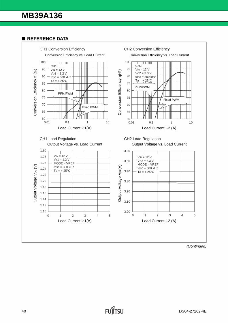
■ REFERENCE DATA
(Continued)
CH1 Conversion Efficiency CH2 Conversion Efficiency
Conversion Efficiency vs. Load Current Conversion Efficiency vs. Load Current
Con
vers
ion
Effi
cien
cy η
(%
)
Con
vers
ion
Effi
cien
cy η
(%)
Load Current IO1(A) Load Current IO2 (A)
CH1 Load Regulation CH2 Load RegulationOutput Voltage vs. Load Current Output Voltage vs. Load Current
Out
put V
olta
ge V
O1
(V)
Out
put V
olta
ge V
O2(
V)
Load Current IO1(A) Load Current IO2 (A)
0.01 0.1 1 1060
65
70
75
80
85
90
95
100CH1VIN = 12 VVO1 = 1.2 Vfosc = 300 kHzTa = + 25°C
PFM/PWM
Fixed PWM
0.01 0.1 1 10
CH2VIN = 12 VVO2 = 3.3 Vfosc = 300 kHzTa = + 25°C
PFM/PWM
60
65
70
75
80
85
90
95
100
Fixed PWM
0 1 2 3 4 5
VIN = 12 VVO1 = 1.2 VMODE = VREFfosc = 300 kHzTa = + 25°C
1.10
1.12
1.14
1.16
1.18
1.20
1.22
1.24
1.26
1.28
1.30
0 1 2 3 4 5
VIN = 12 VVO2 = 3.3 VMODE = VREFfosc = 300 kHzTa = + 25°C
3.00
3.10
3.20
3.30
3.40
3.50
3.60
40 DS04-27262-4E
MB39A136
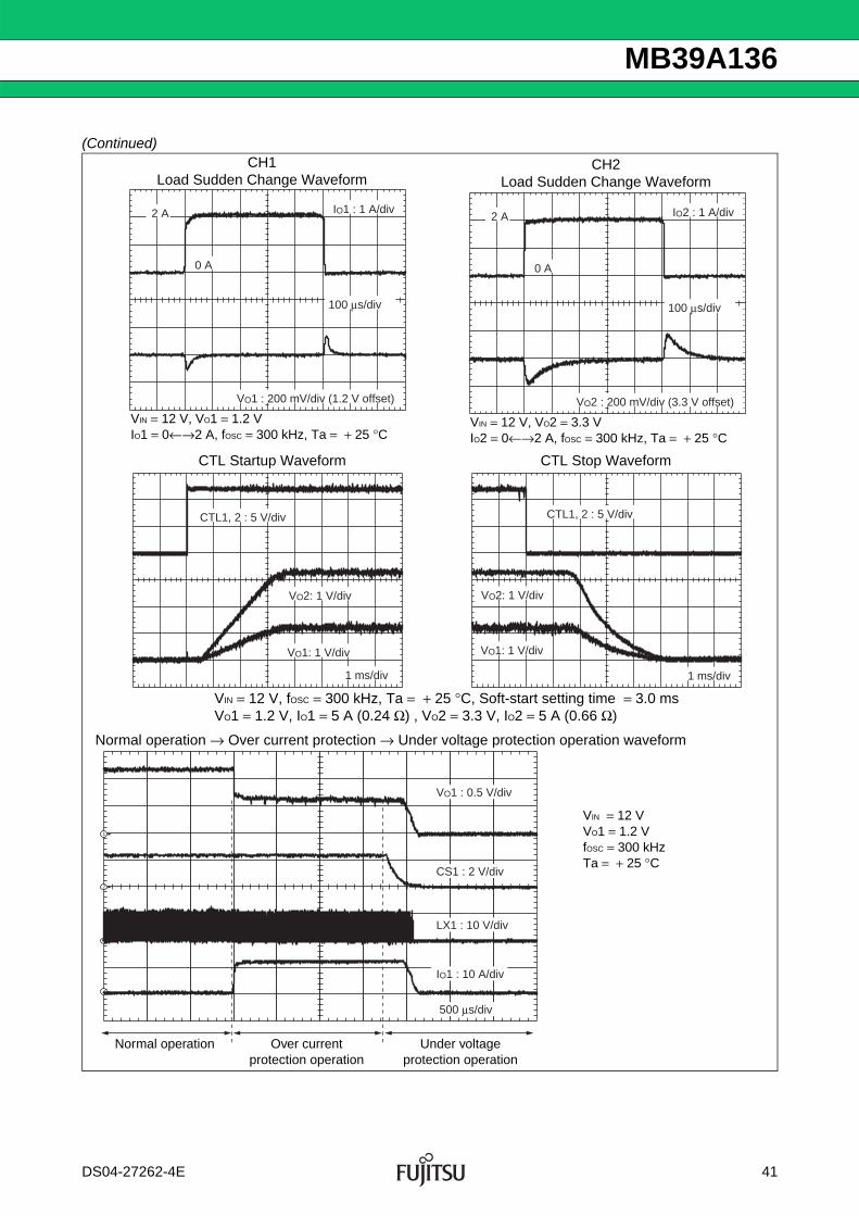
(Continued)
3
4
2
1
VO1 : 0.5 V/div
CS1 : 2 V/div
LX1 : 10 V/div
IO1 : 10 A/div
500 μs/div
VO1: 1 V/div
1 ms/div
VO2: 1 V/div
CTL1, 2 : 5 V/div
VO1: 1 V/div
1 ms/div
VO2: 1 V/div
CTL1, 2 : 5 V/div
2 A
0 A
VO2 : 200 mV/div (3.3 V offset)
100 μs/div
IO2 : 1 A/div
CH1 Load Sudden Change Waveform
CH2 Load Sudden Change Waveform
CTL Startup Waveform CTL Stop Waveform
VIN = 12 V, fOSC = 300 kHz, Ta = + 25 °C, Soft-start setting time = 3.0 msVO1 = 1.2 V, IO1 = 5 A (0.24 Ω) , VO2 = 3.3 V, IO2 = 5 A (0.66 Ω)
Normal operation → Over current protection → Under voltage protection operation waveform
Normal operation
VIN = 12 V, VO1 = 1.2 VIO1 = 0←→2 A, fOSC = 300 kHz, Ta = + 25 °C
VIN = 12 V, VO2 = 3.3 VIO2 = 0←→2 A, fOSC = 300 kHz, Ta = + 25 °C
VIN = 12 VVO1 = 1.2 VfOSC = 300 kHzTa = + 25 °C
Over current protection operation
Under voltage protection operation
2 A
0 A
VO1 : 200 mV/div (1.2 V offset)
100 μs/div
IO1 : 1 A/div
DS04-27262-4E 41
MB39A136
■ USAGE PRECAUTION1. Do not configure the IC over the maximum ratings.
If the IC is used over the maximum ratings, the LSI may be permanently damaged.It is preferable for the device to be normally operated within the recommended usage conditions. Usageoutside of these conditions can have an adverse effect on the reliability of the LSI.
2. Use the device within the recommended operating conditions.
The recommended values guarantee the normal LSI operation under the recommended operating conditions. The electrical ratings are guaranteed when the device is used within the recommended operating conditionsand under the conditions stated for each item.
3. Printed circuit board ground lines should be set up with consideration for common impedance.
4. Take appropriate measures against static electricity.• Containers for semiconductor materials should have anti-static protection or be made of conductive ma-
terial.• After mounting, printed circuit boards should be stored and shipped in conductive bags or containers.• Work platforms, tools, and instruments should be properly grounded.• Working personnel should be grounded with resistance of 250 kΩ to 1 MΩ in series between body and
ground.
5. Do not apply negative voltages.
The use of negative voltages below − 0.3 V may make the parasitic transistor activated, and can causemalfunctions.
42 DS04-27262-4E
MB39A136
■ ORDERING INFORMATION
■ EV BOARD ORDERING INFORMATION
Part number Package Remarks
MB39A136PFT24-pin plastic TSSOP
(FPT-24P-M09)
Part number EV board version No. Remarks
MB39A136EVB-01 MB39A136EVB-01 Rev2.0 TSSOP-24
DS04-27262-4E 43
MB39A136
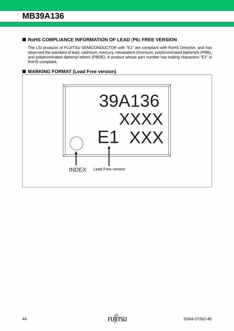
■ RoHS COMPLIANCE INFORMATION OF LEAD (Pb) FREE VERSION
The LSI products of FUJITSU SEMICONDUCTOR with “E1” are compliant with RoHS Directive, and hasobserved the standard of lead, cadmium, mercury, Hexavalent chromium, polybrominated biphenyls (PBB),and polybrominated diphenyl ethers (PBDE). A product whose part number has trailing characters “E1” isRoHS compliant.
■ MARKING FORMAT (Lead Free version)
XXXX39A136
XXXE1
INDEX Lead Free version
44 DS04-27262-4E
MB39A136
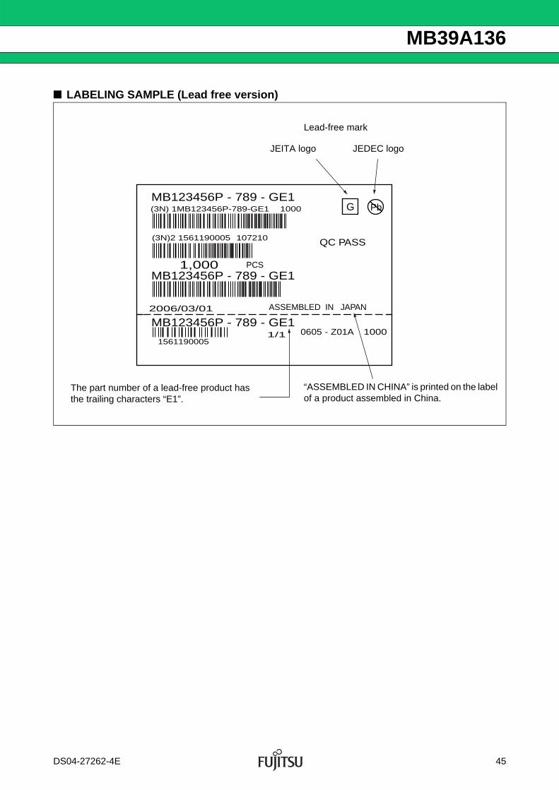
■ LABELING SAMPLE (Lead free version)
2006/03/01 ASSEMBLED IN JAPAN
G
QC PASS
(3N) 1MB123456P-789-GE1 1000
(3N)2 1561190005 107210
1,000 PCS
0605 - Z01A 10001/11561190005
MB123456P - 789 - GE1
MB123456P - 789 - GE1
MB123456P - 789 - GE1
Pb
Lead-free mark
JEITA logo JEDEC logo
The part number of a lead-free product has the trailing characters “E1”.
“ASSEMBLED IN CHINA” is printed on the label of a product assembled in China.
DS04-27262-4E 45
MB39A136
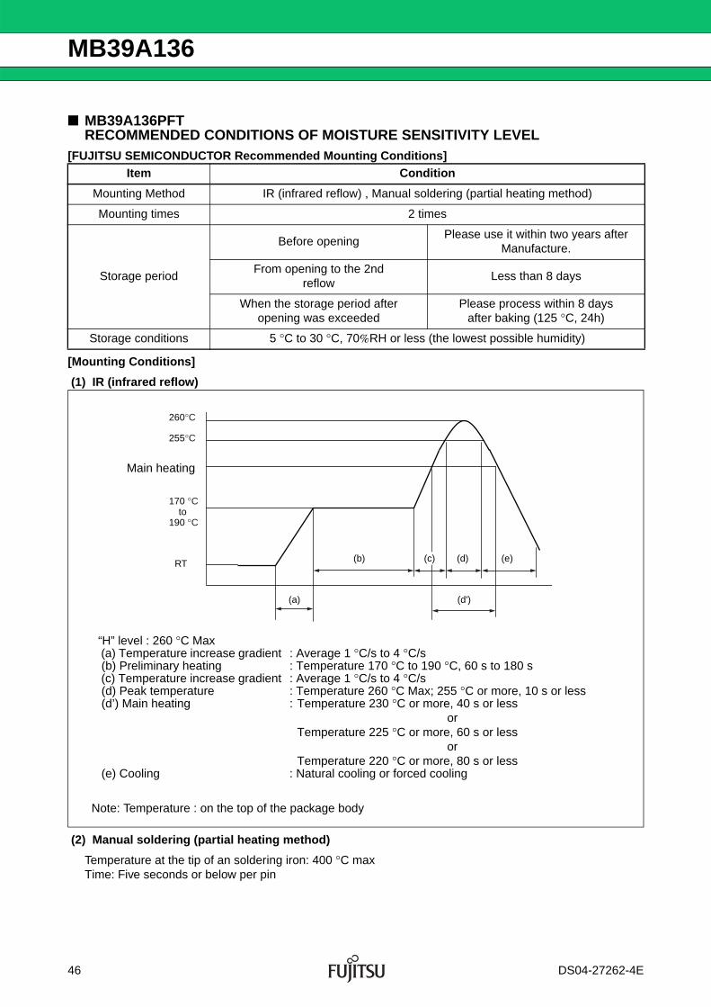
■ MB39A136PFTRECOMMENDED CONDITIONS OF MOISTURE SENSITIVITY LEVEL
[FUJITSU SEMICONDUCTOR Recommended Mounting Conditions]
[Mounting Conditions]
(1) IR (infrared reflow)
(2) Manual soldering (partial heating method)
Temperature at the tip of an soldering iron: 400 °C maxTime: Five seconds or below per pin
Item Condition
Mounting Method IR (infrared reflow) , Manual soldering (partial heating method)
Mounting times 2 times
Storage period
Before opening Please use it within two years after
Manufacture.
From opening to the 2ndreflow
Less than 8 days
When the storage period afteropening was exceeded
Please process within 8 daysafter baking (125 °C, 24h)
Storage conditions 5 °C to 30 °C, 70%RH or less (the lowest possible humidity)
260°C
(e)
(d')
(d)
255°C
170 °C
190 °C
RT (b)
(a)
(c)
to
Note: Temperature : on the top of the package body
“H” level : 260 °C Max (a) Temperature increase gradient : Average 1 °C/s to 4 °C/s (b) Preliminary heating : Temperature 170 °C to 190 °C, 60 s to 180 s (c) Temperature increase gradient : Average 1 °C/s to 4 °C/s (d) Peak temperature : Temperature 260 °C Max; 255 °C or more, 10 s or less (d’) Main heating : Temperature 230 °C or more, 40 s or less
orTemperature 225 °C or more, 60 s or less
orTemperature 220 °C or more, 80 s or less
(e) Cooling : Natural cooling or forced cooling
Main heating
46 DS04-27262-4E
MB39A136
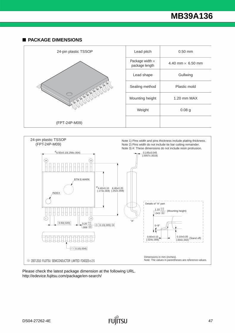
■ PACKAGE DIMENSIONS
Please check the latest package dimension at the following URL.http://edevice.fujitsu.com/package/en-search/
24-pin plastic TSSOP Lead pitch 0.50 mm
Package width ×package length
4.40 mm × 6.50 mm
Lead shape Gullwing
Sealing method Plastic mold
Mounting height 1.20 mm MAX
Weight 0.08 g
24-pin plastic TSSOP(FPT-24P-M09)
(FPT-24P-M09)
C 2007-2010 FUJITSU SEMICONDUCTOR LIMITED F24032S-c-2-5
6.50±0.10(.256±.004)#
4.40±0.10 6.40±0.20(.252±.008)(.173±.004)
#
0.10±0.05
(Mounting height)
0.10(.004)
0.50(.020)
1 12
24 13
"A"
(Stand off)
0.145±0.045(.0057±.0018)
M0.13(.005)
Details of "A" part
0~8°
(.024±.006)0.60±0.15
INDEX
(.004±.002)
BTM E-MARK
1.10+0.10
+.004
–0.15
–.006.043
0.20+0.07
+.003
–0.02
–.001.008
Dimensions in mm (inches).Note: The values in parentheses are reference values.
Note 1) Pins width and pins thickness include plating thickness.Note 2) Pins width do not include tie bar cutting remainder.Note 3) #: These dimensions do not include resin protrusion.
DS04-27262-4E 47
MB39A136
■ MAJOR CHANGES IN THIS EDITIONA change on a page is indicated by a vertical line drawn on the left side of that page.
Page Section Change Results
9■ ELECTRICAL CHARACTERISTICS Revised the minimum value of “Maximum on-duty” in
“Output Block [DRV]”: 72 → 75
48 DS04-27262-4E
MB39A136
■ CONTENTSpage
- DESCRIPTION .................................................................................................................................................... 1- FEATURES .......................................................................................................................................................... 1- APPLICATION ..................................................................................................................................................... 1- PIN ASSIGNMENT ............................................................................................................................................. 2- PIN DESCRIPTION ............................................................................................................................................ 3- BLOCK DIAGRAM .............................................................................................................................................. 4- ABSOLUTE MAXIMUM RATINGS ................................................................................................................... 5- RECOMMENDED OPERATING CONDITIONS ............................................................................................ 6- ELECTRICAL CHARACTERISTICS ................................................................................................................ 7- TYPICAL CHARACTERISTICS ........................................................................................................................ 11- FUNCTION DESCRIPTION .............................................................................................................................. 13- PROTECTION FUNCTION TABLE .................................................................................................................. 17- I/O PIN EQUIVALENT CIRCUIT DIAGRAM ................................................................................................... 18- EXAMPLE APPLICATION CIRCUIT ................................................................................................................ 20- PARTS LIST ......................................................................................................................................................... 21- APPLICATION NOTE ......................................................................................................................................... 23- REFERENCE DATA ........................................................................................................................................... 40- USAGE PRECAUTION ...................................................................................................................................... 42- ORDERING INFORMATION ............................................................................................................................. 43- EV BOARD ORDERING INFORMATION ....................................................................................................... 43- RoHS COMPLIANCE INFORMATION OF LEAD (Pb) FREE VERSION ................................................... 44- MARKING FORMAT (Lead Free version) ....................................................................................................... 44- LABELING SAMPLE (Lead free version) ........................................................................................................ 45- MB39A136PFT RECOMMENDED CONDITIONS OF MOISTURE SENSITIVITY LEVEL ..................... 46- PACKAGE DIMENSIONS .................................................................................................................................. 47- MAJOR CHANGES IN THIS EDITION ............................................................................................................ 48
DS04-27262-4E 49
MB39A136
MEMO
50 DS04-27262-4E
MB39A136
MEMO
DS04-27262-4E 51
MB39A136
FUJITSU SEMICONDUCTOR LIMITEDNomura Fudosan Shin-yokohama Bldg. 10-23, Shin-yokohama 2-Chome,Kohoku-ku Yokohama Kanagawa 222-0033, JapanTel: +81-45-415-5858http://jp.fujitsu.com/fsl/en/
For further information please contact:
North and South AmericaFUJITSU SEMICONDUCTOR AMERICA, INC.1250 E. Arques Avenue, M/S 333Sunnyvale, CA 94085-5401, U.S.A.Tel: +1-408-737-5600 Fax: +1-408-737-5999http://us.fujitsu.com/micro/
EuropeFUJITSU SEMICONDUCTOR EUROPE GmbHPittlerstrasse 47, 63225 Langen, GermanyTel: +49-6103-690-0 Fax: +49-6103-690-122http://emea.fujitsu.com/semiconductor/
KoreaFUJITSU SEMICONDUCTOR KOREA LTD.902 Kosmo Tower Building, 1002 Daechi-Dong,Gangnam-Gu, Seoul 135-280, Republic of KoreaTel: +82-2-3484-7100 Fax: +82-2-3484-7111http://kr.fujitsu.com/fsk/
Asia PacificFUJITSU SEMICONDUCTOR ASIA PTE. LTD.151 Lorong Chuan,#05-08 New Tech Park 556741 SingaporeTel : +65-6281-0770 Fax : +65-6281-0220http://sg.fujitsu.com/semiconductor/
FUJITSU SEMICONDUCTOR SHANGHAI CO., LTD.30F, Kerry Parkside, 1155 Fang Dian Road, Pudong District,Shanghai 201204, ChinaTel : +86-21-6146-3688 Fax : +86-21-6146-3660http://cn.fujitsu.com/fss/
FUJITSU SEMICONDUCTOR PACIFIC ASIA LTD.2/F, Green 18 Building, Hong Kong Science Park,Shatin, N.T., Hong KongTel : +852-2736-3232 Fax : +852-2314-4207http://cn.fujitsu.com/fsp/
Specifications are subject to change without notice. For further information please contact each office.
All Rights Reserved.The contents of this document are subject to change without notice. Customers are advised to consult with sales representatives before ordering.The information, such as descriptions of function and application circuit examples, in this document are presented solely for the purposeof reference to show examples of operations and uses of FUJITSU SEMICONDUCTOR device; FUJITSU SEMICONDUCTOR doesnot warrant proper operation of the device with respect to use based on such information. When you develop equipment incorporatingthe device based on such information, you must assume any responsibility arising out of such use of the information. FUJITSU SEMICONDUCTOR assumes no liability for any damages whatsoever arising out of the use of the information.Any information in this document, including descriptions of function and schematic diagrams, shall not be construed as license of the useor exercise of any intellectual property right, such as patent right or copyright, or any other right of FUJITSU SEMICONDUCTOR or anythird party or does FUJITSU SEMICONDUCTOR warrant non-infringement of any third-party's intellectual property right or other rightby using such information. FUJITSU SEMICONDUCTOR assumes no liability for any infringement of the intellectual property rights orother rights of third parties which would result from the use of information contained herein.The products described in this document are designed, developed and manufactured as contemplated for general use, including withoutlimitation, ordinary industrial use, general office use, personal use, and household use, but are not designed, developed and manufacturedas contemplated (1) for use accompanying fatal risks or dangers that, unless extremely high safety is secured, could have a serious effectto the public, and could lead directly to death, personal injury, severe physical damage or other loss (i.e., nuclear reaction control innuclear facility, aircraft flight control, air traffic control, mass transport control, medical life support system, missile launch control inweapon system), or (2) for use requiring extremely high reliability (i.e., submersible repeater and artificial satellite).Please note that FUJITSU SEMICONDUCTOR will not be liable against you and/or any third party for any claims or damages aris-ing in connection with above-mentioned uses of the products.Any semiconductor devices have an inherent chance of failure. You must protect against injury, damage or loss from such failuresby incorporating safety design measures into your facility and equipment such as redundancy, fire protection, and prevention of over-current levels and other abnormal operating conditions.Exportation/release of any products described in this document may require necessary procedures in accordance with the regulationsof the Foreign Exchange and Foreign Trade Control Law of Japan and/or US export control laws.The company names and brand names herein are the trademarks or registered trademarks of their respective owners.
Edited: Sales Promotion Department