Embed Size (px)
Citation preview
SpaceFibre Interface Chip
Final Presentation
1st June 2021

Final Presentation Agenda
▪ Introduction
▪ SpaceFibre Interface Chip Architecture
▪ SpaceFibre Interface Chip Verification and Validation
▪ ASIC Feasibility
▪ Conclusions
2
SpaceFibre Interface Chip
Introduction
Steve Parkes, CTO STAR-Dundee Ltd.
Felix Siegle, ESA Technical Officer
SpaceFibre
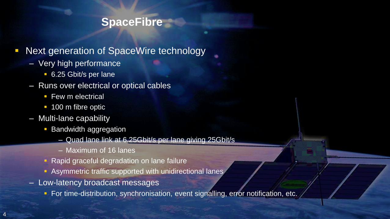
▪ Next generation of SpaceWire technology
– Very high performance
▪ 6.25 Gbit/s per lane
– Runs over electrical or optical cables
▪ Few m electrical
▪ 100 m fibre optic
– Multi-lane capability
▪ Bandwidth aggregation
– Quad lane link at 6.25Gbit/s per lane giving 25Gbit/s
– Maximum of 16 lanes
▪ Rapid graceful degradation on lane failure
▪ Asymmetric traffic supported with unidirectional lanes
– Low-latency broadcast messages
▪ For time-distribution, synchronisation, event signalling, error notification, etc.
4
SpaceFibre
▪ Next generation of SpaceWire technology
– Novel quality of service
▪ Up to 32 virtual channels
▪ Priority, bandwidth reservation and scheduling
– Virtual networks
▪ Constructed with virtual channels
▪ Acting as independent networks over a single physical network
– Innovative fault detection, isolation and recovery
▪ At the link level enabling rapid error recovery (few microseconds)
▪ Babbling node/virtual channel protection
▪ Graceful degradation of multi-lane link
▪ Multi-lane link technology patented – free of charge licence for space applications
– Small footprint
▪ Taking a few percent of a recent radiation tolerant FPGA
– Straightforward to integrate with existing SpaceWire equipment5
OPS-SAT Image courtesy of ESA
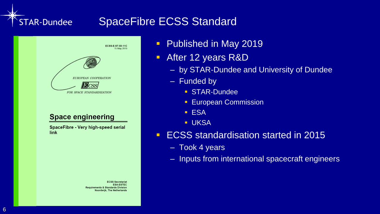
SpaceFibre ECSS Standard
▪ Published in May 2019
▪ After 12 years R&D
– by STAR-Dundee and University of Dundee
– Funded by
▪ STAR-Dundee
▪ European Commission
▪ ESA
▪ UKSA
▪ ECSS standardisation started in 2015
– Took 4 years
– Inputs from international spacecraft engineers
6
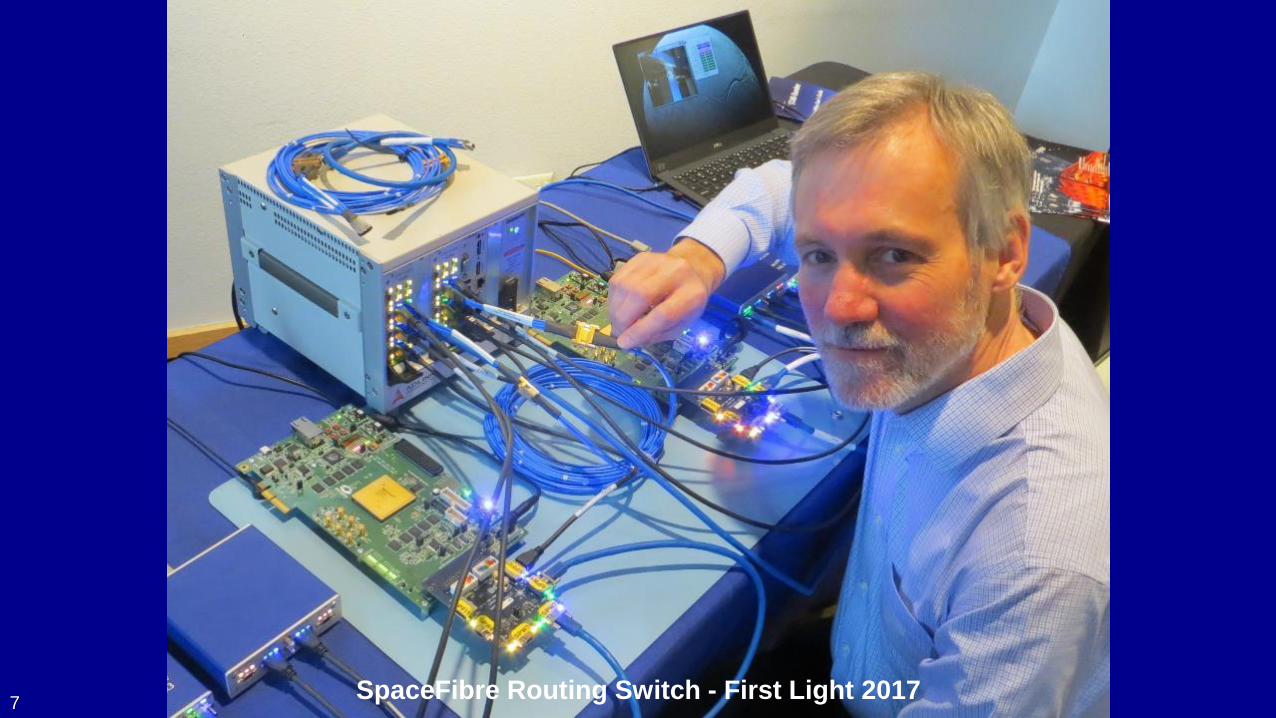
7SpaceFibre Routing Switch - First Light 2017

Study Aims
▪ Design a high-performance, versatile SpaceFibre interface chip to:
– Bridge between existing SpaceWire devices and a SpaceFibre network
▪ Provide the QoS and FDIR capabilities of SpaceFibre to the SpaceWire traffic
▪ Reduce cable mass and simplifying redundancy schemes
– Collect data from high data-rate instruments and send it to a mass-memory unit
▪ Interface to an FPGA or ASIC inside the instrument (or other equipment)
▪ To collect the high data-rate data
▪ Support data rates in the range of 1 to 5 Gbit/s
– Support configuration, control and monitoring of the instrument
▪ Using the same network connection as is used for transferring data
– Provide an easy migration path for existing equipment
▪ That uses Wizard Link or Channel Link technology
▪ Provide the full capabilities of SpaceFibre in the chip
8

Study Aims
– Provide existing processing devices with a SpaceFibre interface so that they can:
▪ Process data provided over SpaceFibre
▪ Control equipment over a SpaceFibre network
– Connect to COTS processors
▪ Using an Gigabit Ethernet interface
– Program reprogrammable FPGAs over a network
▪ In support of reconfigurable processing systems
– Provide time-distribution, event synchronisation and error reporting services
▪ Using the SpaceFibre broadcast mechanism
9

Study Activities
10
WP1100 (STAR)Requirements Collation
and Review
WP1200 (Airbus DS)Radar and Optical
Instrument Use Cases and Requirements
WP2100 (STAR)Chip Specification
WP2200 (Airbus DS)Specification Review and Instrument External Test
Plan
WP2300 (RUAG Space)Specification Review and
Avionics Equipment External Test Plan
WP3100 (STAR)RTL Implementation, Simulation and Test
WP6100 (STAR)Test Support and Issue
Resolution
WP5100 (STAR)Test Equipment & Test
Software
WP1300 (RUAG Space)Avionics Equipment Use Cases and Requirements
WP1400 (ISD)ASIC Requirements
WP4100 (STAR)FPGA Place & Route &
Test
WP4200 (STAR)Breadboard
Implementation
WP6200 (Airbus DS)Instrument External Test
Plan and Application Oriented Testing
WP6300 (RUAG Space)Avionics Equipment
External Test Plan and Applic. Oriented Testing
TASK 1Requirements
TASK 2Specification
TASK 3Architectural Design
TASK 5Testing
TASK 4Breadboarding
SpaceFibre Interface Chip
Task 6External Testing
WP7100 (STAR)Collate Critical Review and Flight Model Plans
WP7200 (Airbus DS)Inputs to Flight Model
Plans &Redundancy Approach
WP7300 (RAUG Space)Inputs to Flight Model
Plans
Task 7Critical Review & Plan
WP8100 (STAR)Management and End of
Contract Reporting
WP8200 (Airbus DS)Airbus DS Management
and Inputs to Final Report
WP8300 (RUAG Space)RUAG Space Management and Inputs to Final Report
Management
= STAR-Dundee
= Airbus DS
= RUAG Space
= ISD
WP1500 (Airbus DS)Reliability and Redundancy
Requirements
WP2400 (ISD)Packaging Specifications
WP5200 (STAR)Initial Testing &
Bug Fixes
WP7400 (ISD)Radiation Hardening
Packaging &Qualification
WP4300 (STAR)FPGA Verification
WP8400 (ISD)ISD Management and Inputs to Final Report
WP2500 (STAR)Breadboard and Demo. Environment Spec. and
Test Plan
WP3200 (ISD)Preliminary Front-End
Flow Execution for 65nm CMOS process
SpaceFibre Interface Chip
Architecture
12
13

14

Parallel IO Modes of Operation
Parallel IO Mode SpW Interfaces Parallel Inputs Parallel Outputs GMII Interfaces
SpW Bridge 12 0 0 0
Parallel TX 2 2 0 0
Parallel RX 2 0 2 0
Parallel TX/RX 2 1 1 0
Parallel TX/GMII 2 1 0 1
Parallel RX/GMII 2 0 1 1
Parallel TX/SpW Bridge 7 1 0 0
Parallel RX/SpW Bridge 7 0 1 0
GMII/SpW Bridge 7 0 0 1
15

GPIO Functions
16
Table 5-7 GPIO Functions and IO Pin Sharing
S3 S2 S1 S0 Mode GPIO[31:24] GPIO[23:16] GPIO[15:8] GPIO[7:0]
0 0 0 0 Status0 Status[31:24] Status[23:16] Status[15:8] Status[7:0]
0 0 0 1 Status1 Status[63:56] Status[55:48] Status[47:40] Status[39:32]
0 0 1 0 BM RX BC[7:0] BType[7:0] BData[15:8] BData[7:0]
0 0 1 1 BM TS BData[31:24] BData[23:16] BData[15:8] Time-Slot[7:0]
0 1 0 0 Time0 Seconds[15:8] Seconds[7:0] FracSecs[1:8] FracSecs[9:16]
0 1 0 1 Time1 Seconds[23:16] Seconds[15:8] Seconds[7:0] FracSecs[1:8]
0 1 1 0 DataOut DOut[31:24] DOut[23:16] DOut[15:8] DOut[7:0]
0 1 1 1 Config
1 0 0 0 DataIn DIn[31:24] DIn[23:16] DIn[15:8] DIn[7:0]
1 0 0 1 DataIO DIn[15:8] DIn[7:0] DOut[15:8] DOut[7:0]
1 0 1 0 BM TX BC[7:0] BType[7:0] BData[15:8] BData[7:0]
1 0 1 1 SPI/I2C SPI/I2C7,6 SPI/I2C5,4 SPI/I2C3,2 SPI/I2C1,0
1 1 0 0 FPGA0 SlctMAP D[7:0] SlctMAP Cntrl DIn[7:0] DOut[7:0]
1 1 0 1 FPGA1 JTAG SPI/I2C5,4 DIn[7:0] DOut[7:0]
1 1 1 0 FPGA2 SlctMAP D[7:0] SlctMAP Cntrl SPI/I2C3,2 Time-Slot[7:0]
1 1 1 1 FPGA3 JTAG SPI/I2C5,4 SPI/I2C3,2 Time-Slot[7:0]
SpaceFibre Interface Chip
FPGA and FMC Board

SpaceFibre Interface Chip Development
▪ Designed in VHDL
▪ Extensively simulated and tested
▪ Implemented in FPGA hardware
– On a specially designed FMC board
▪ Tested by STAR-Dundee
– SpaceWire Bridge and GPIO testing
▪ Using SpaceWire Bridge and GPIO Test board
– Parallel and Ethernet interface testing
▪ Using Parallel/GMII Test board
▪ Tested by Airbus
– Remote FPGA programming over SpaceFibre
18
19
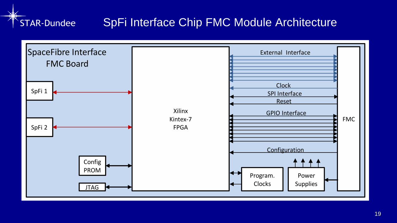
SpFi Interface Chip FMC Module Architecture
FMCFMC
JTAG
XilinxKintex-7
FPGA
Power Supplies
Program.Clocks
SpFi 1
SpFi 2
ConfigPROM
External Interface
GPIO Interface
SPI InterfaceReset
Clock
SpaceFibre InterfaceFMC Board
Configuration

20
SpFi Interface Chip FMC Module
VITA 57 FMC board
Kintex 7 FPGA
Compatible with Xilinx and other FPGA development boards
Available for purchase from STAR-Dundee
SpaceFibre Interface Chip
SpaceWire Bridge and GPIO Test Board
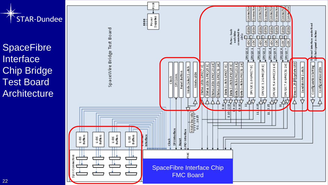
SpaceFibre
Interface
Chip Bridge
Test Board
Architecture
22
SpaceFibre Interface Chip
FMC Board

SpaceWire Bridge Test Board
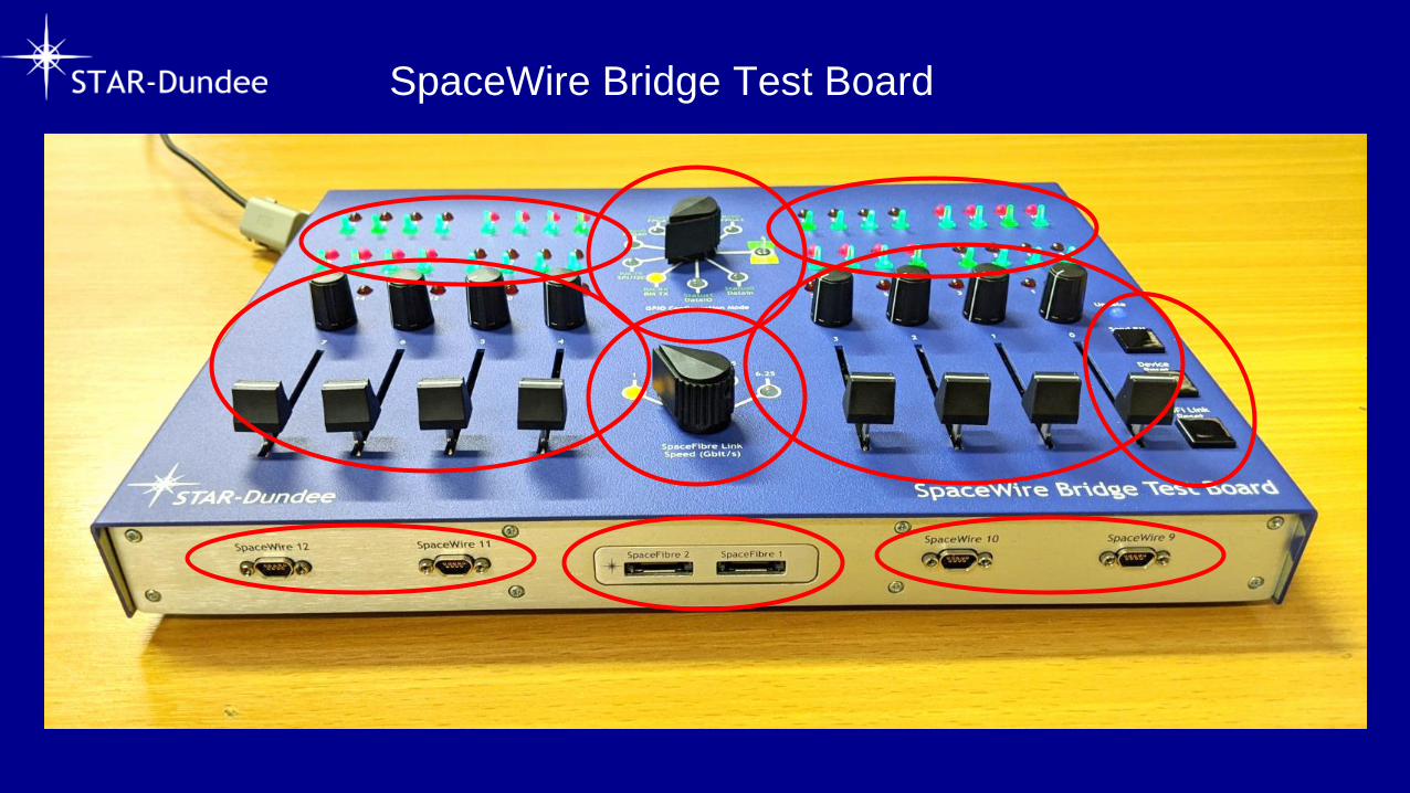
SpaceWire Bridge Test Board
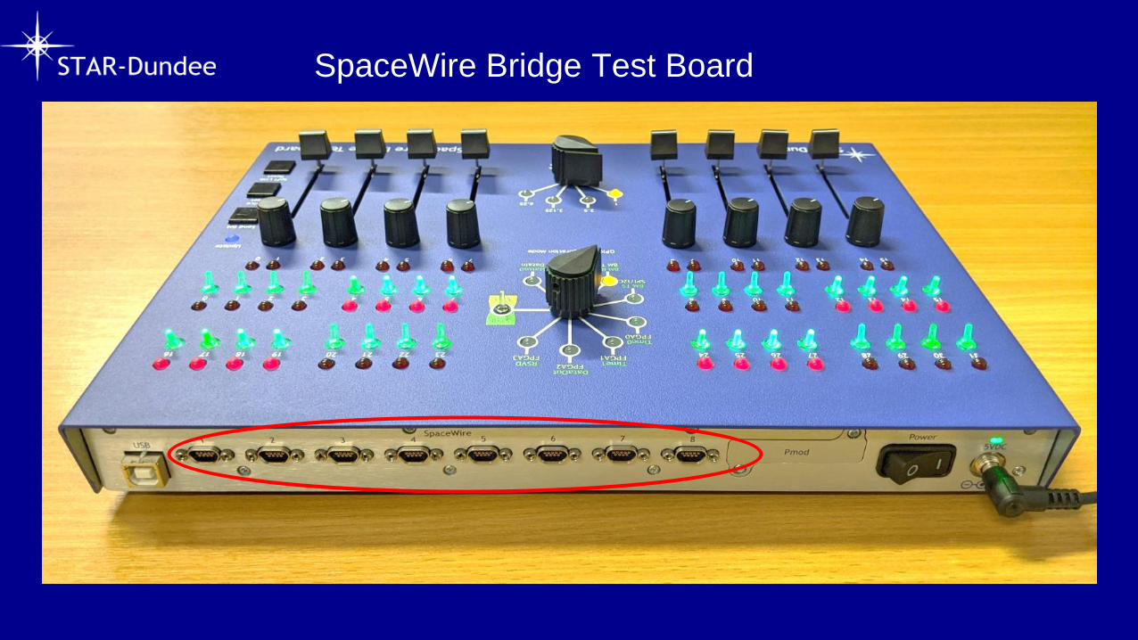
SpaceWire Bridge Test Board

STAR Fire Mk3
26
USB
3 In
terf
ace
Chan 0
Chan 2
SpWRouter
RMAP
SpW 1
SpW 2
SpFi 1
Pattern Gen x8
Pattern Chk x8
1
2
3
VC0VC1…
VC7Configuration Bus
67-8/9-10 SpW/SpFi
Bridge
Chan 1 4
5
RateAdjust
RateAdjust
RateAdjust
RateAdjust
Memory SpFi Analyser
VC0VC1…
VC7
SpFi 2
STAR Fire Mk3

Tests with SpaceWire Bridge Set-Up
▪ SpaceWire Bridge Tests
– Sending and Receiving SpaceWire Data over SpaceFibre
– GPIO tests
– Remote FPGA programming over SpaceFibre using JTAG
27

SpaceWire Bridge Test Architecture
28
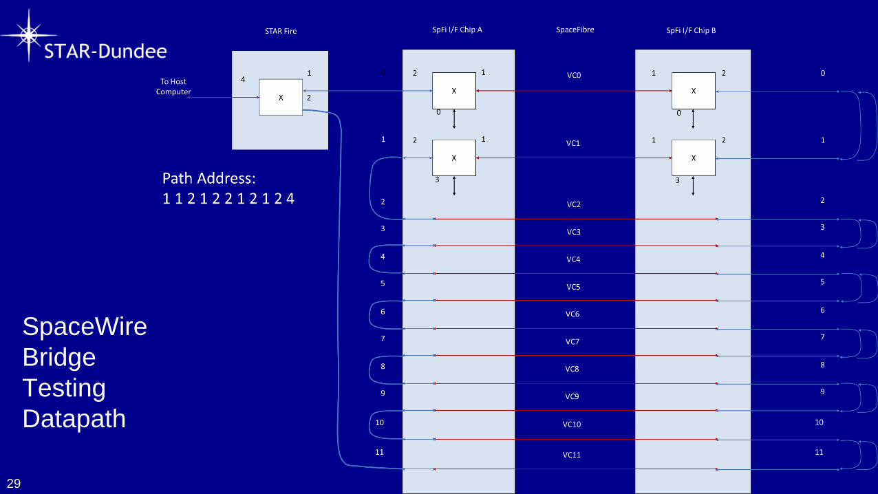
SpaceWire
Bridge
Testing
Datapath
29

SpaceWire Bridge Test Hardware Setup
30

SpaceWire Bridge Testing Results
31
200Mbit/s SpW link speed
154Mbit/s each SpW I/F
x 12 VCs
= 1.85Gbit/s
Design supports 400Mbit/s
SpW
= 3.7Gbit/s in each direction

FPGA Configuration Tests
▪ Uses the Parallel Test Set-Up
▪ FPGA Configuration Tests:
– Configuring the Test FPGA over SpaceFibre using SelectMAP
▪ Using the Parallel/GMII Test Board
– Configuring the Test FPGA over SpaceFibre using JTAG
▪ Using the SpaceWire Bridge test Board
▪ Final testing carried out by Airbus GmbH
32
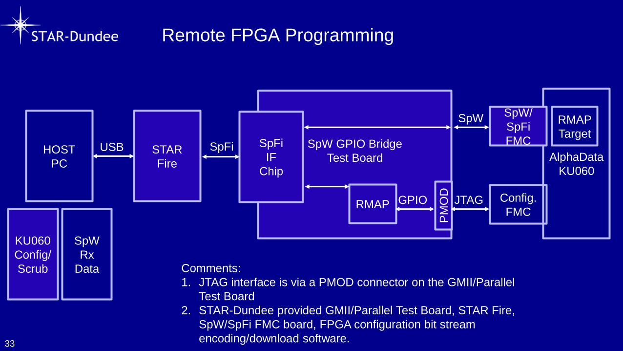
AlphaData
KU060
SpW GPIO Bridge
Test Board
SpFi
IF
Chip
STAR
Fire
SpW/
SpFi
FMC
RMAP
PM
OD
Remote FPGA Programming
33
GPIO
USB
SpW
HOST
PC
KU060
Config/
Scrub
SpW
Rx
Data
JTAG
RMAP
Target
Comments:
1. JTAG interface is via a PMOD connector on the GMII/Parallel
Test Board
2. STAR-Dundee provided GMII/Parallel Test Board, STAR Fire,
SpW/SpFi FMC board, FPGA configuration bit stream
encoding/download software.
SpFi
Config.
FMC
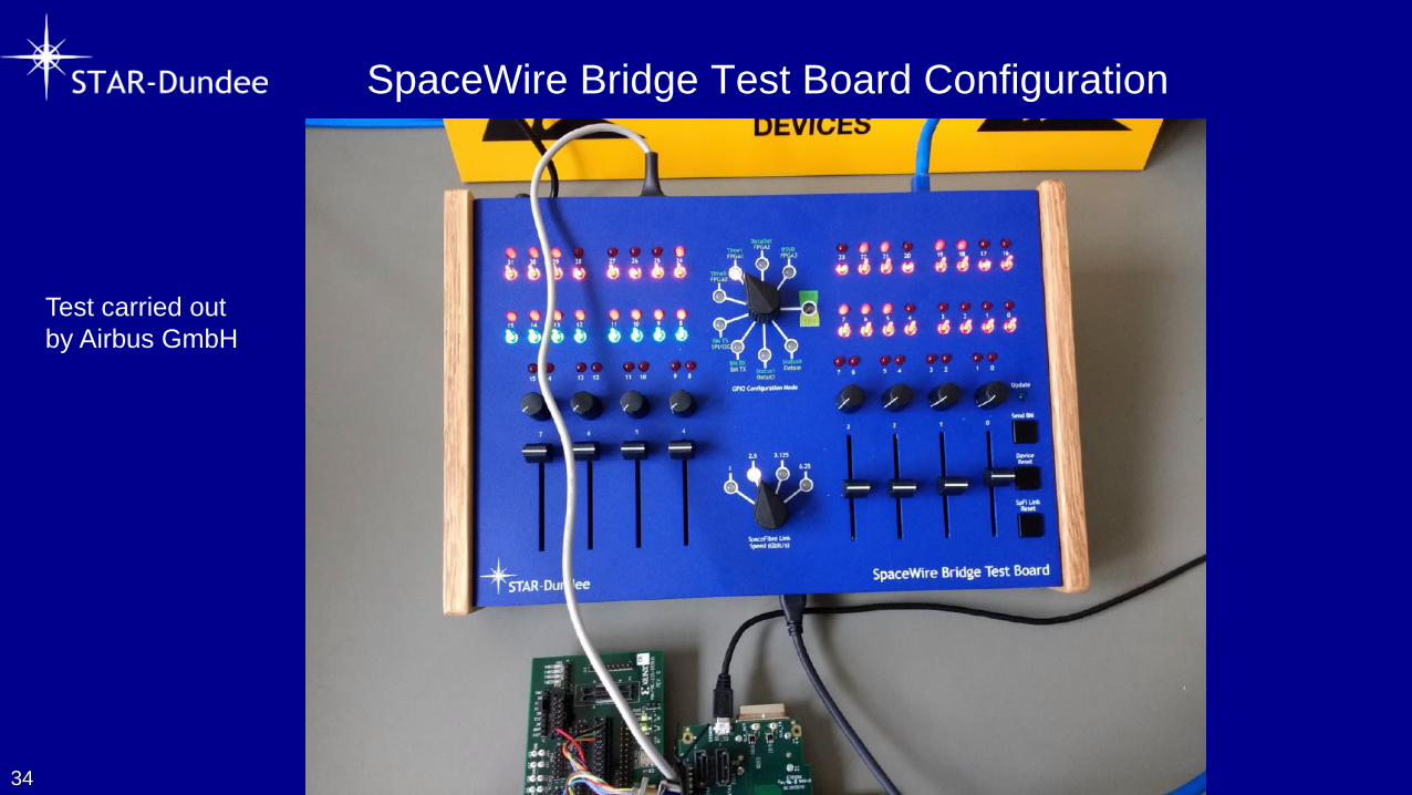
SpaceWire Bridge Test Board Configuration
34
Test carried out
by Airbus GmbH
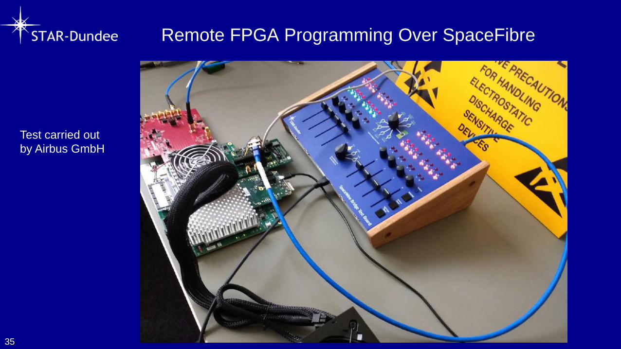
Remote FPGA Programming Over SpaceFibre
35
Test carried out
by Airbus GmbH

SpaceFibre Interface Chip
Parallel and GMII Test Board
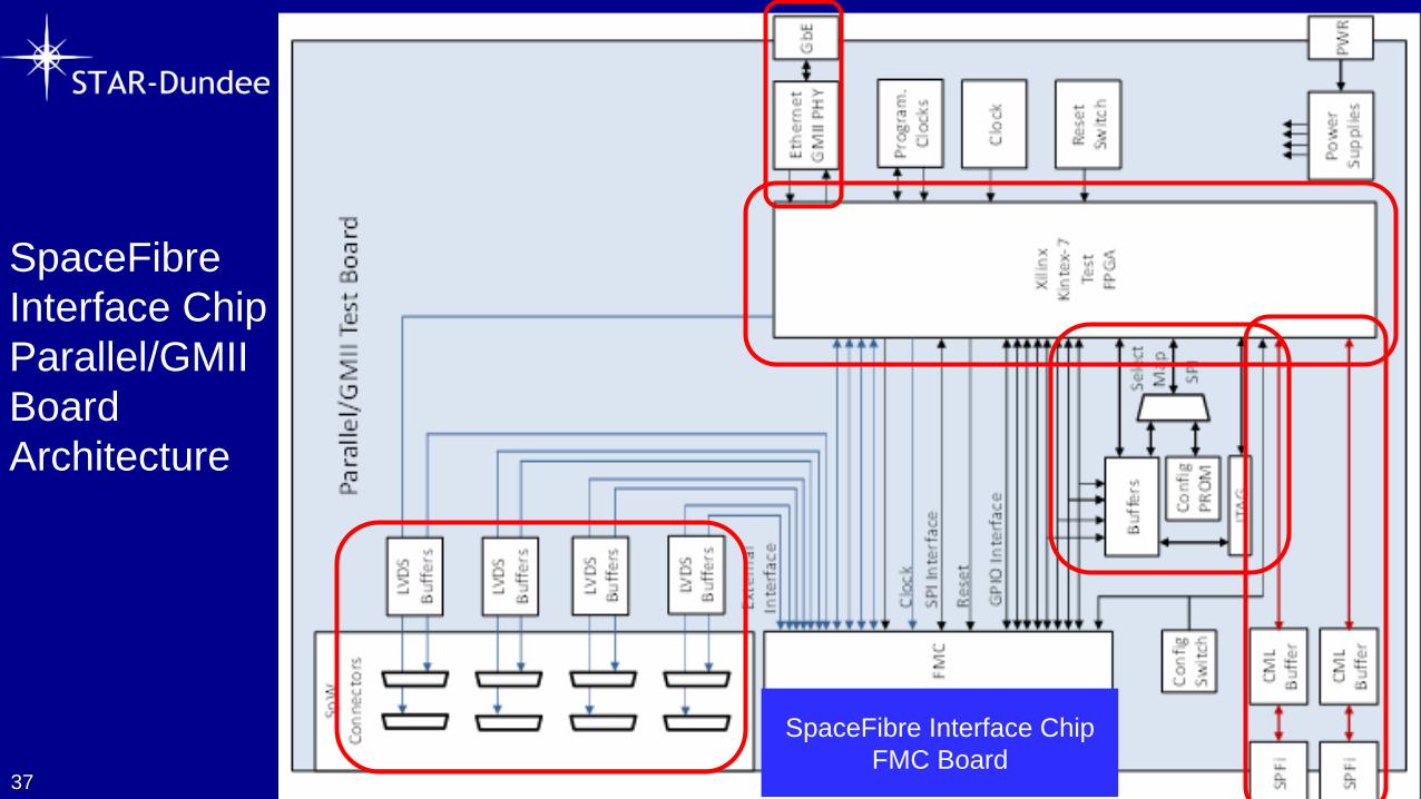
SpaceFibre
Interface Chip
Parallel/GMII
Board
Architecture
37
SpaceFibre Interface Chip
FMC Board

Parallel/GMII Test Board
38

Parallel/GMII Test Board
39

Tests with Parallel/GMII Test Setup
▪ Parallel Interface Tests
– Sending Data from the Parallel-TX Interface over SpaceFibre
– Receiving Data from the Parallel-RX Interface over SpaceFibre
▪ GMII Tests
– Sending and receiving data over Ethernet via GMII interface
40

Parallel
Test Set-up
41
SpWConnectors
FMC
JTAG
XilinxKintex-7
TestFPGA
Power Supplies
Clock
ConfigPROM
ExternalInterface
GPIO Interface
SPI Interface
Reset
ClockProgram.
Clocks
CMLBuffer
SpFi A
CMLBuffer
SpFi B PWR
Parallel/GMII Test Board
Buffers SelectMap
SPIConfigSwitch
ResetSwitch
LVDSBuffers
LVDSBuffers
LVDSBuffers
LVDSBuffers
USB
3 I
nte
rfac
e
Chan 0
Chan 2
SpWRouter
RMAP
SpW 1
SpW 2
SpFi 1
Pattern Gen x8
Pattern Chk x8
1
2
3
VC0VC1…
VC7
Configuration Bus
67-8/9-10
SpW/SpFiBridge
Chan 14
RateAdjustRate
Adjust
RateAdjust
RateAdjust
Memory SpFi Analyser
VC0VC1…
VC7
SpFi 2
STAR Fire Mk3
To HostComputer
FMCFMC
JTAG
SpaceFibreInterface
ChipFPGA
Power Supplies
Program.Clocks
SpFi 1
SpFi 2
ConfigPROM
CMLBuffer
CMLBuffer
External Interface
GPIO Interface
SPI InterfaceReset
Clock
SpaceFibre Interface ChipFPGA Board
Configuration
SpW0
SpW8
SpW9
SpW11
SpW1
SpW7
SpW10
Ethernet GMII PHY
GbE

Parallel Interface Test Setup
42

Parallel Interface Testing
43
32-bit word
every 16ns
= 2Gbit/s

Parallel Interface Testing
44
1.91 Gbit/sClose to 100%
link utilisation

GMII
Test Set-Up
45
SpWConnectors
FMC
JTAG
XilinxKintex-7
TestFPGA
Power Supplies
Clock
ConfigPROM
ExternalInterface
GPIO Interface
SPI Interface
Reset
ClockProgram.
Clocks
CMLBuffer
SpFi A
CMLBuffer
SpFi B PWR
Parallel/GMII Test Board
Buffers SelectMap
SPIConfigSwitch
ResetSwitch
LVDSBuffers
LVDSBuffers
LVDSBuffers
LVDSBuffers
USB
3 I
nte
rfac
e
Chan 0
Chan 2
SpWRouter
RMAP
SpW 1
SpW 2
SpFi 1
Pattern Gen x8
Pattern Chk x8
1
2
3
VC0VC1…
VC7
Configuration Bus
6
7-8/9-10
SpW/SpFiBridge
Chan 14
RateAdjustRate
Adjust
RateAdjust
RateAdjust
Memory SpFi Analyser
VC0VC1…
VC7
SpFi 2
STAR Fire Mk3
To HostComputer
FMCFMC
JTAG
SpaceFibreInterface
ChipFPGA
Power Supplies
Program.Clocks
SpFi 1
SpFi 2
ConfigPROM
CMLBuffer
CMLBuffer
External Interface
GPIO Interface
SPI InterfaceReset
Clock
SpaceFibre Interface ChipFPGA Board
Configuration
SpW0
SpW8
SpW9
SpW11
SpW1
SpW7
SpW10
Ethernet GMII PHY
GbE
To HostComputer
GMII Test Setup
46
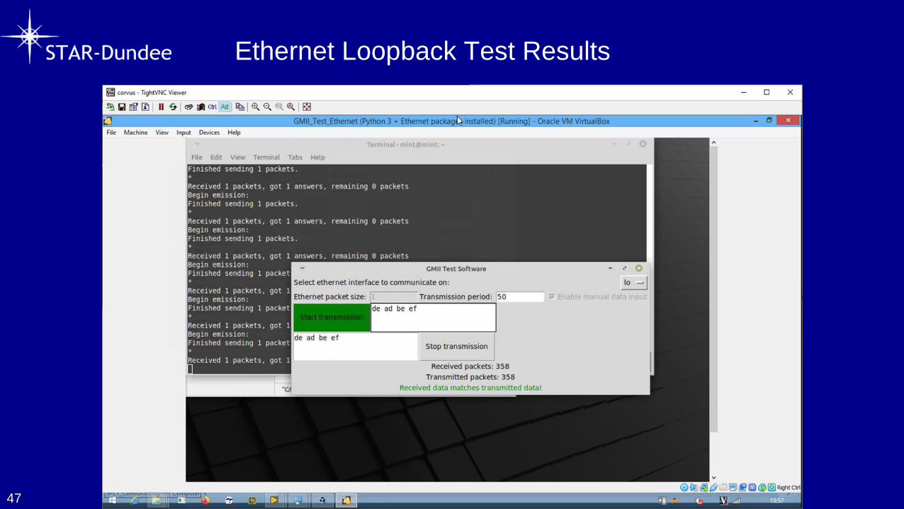
Ethernet Loopback Test Results
47

SpaceFibre Interface Chip
ASIC Feasibility

ASIC Feasibility
▪ ASIC feasibility was carried out by ISD
– With support from STAR-Dundee
▪ Target technology
– C65SPACE
▪ Technology and packaging is qualified
▪ Radiation tolerance well characterised
– Could also consider finer technology e.g. 28nm
▪ Principally for improved SerDes
49
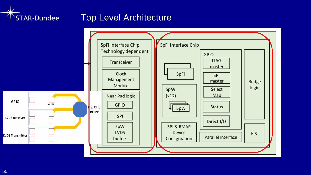
Top Level Architecture
50
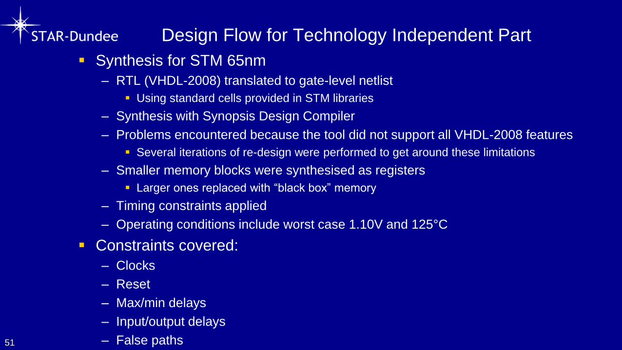
Design Flow for Technology Independent Part
▪ Synthesis for STM 65nm
– RTL (VHDL-2008) translated to gate-level netlist
▪ Using standard cells provided in STM libraries
– Synthesis with Synopsis Design Compiler
– Problems encountered because the tool did not support all VHDL-2008 features
▪ Several iterations of re-design were performed to get around these limitations
– Smaller memory blocks were synthesised as registers
▪ Larger ones replaced with “black box” memory
– Timing constraints applied
– Operating conditions include worst case 1.10V and 125°C
▪ Constraints covered:
– Clocks
– Reset
– Max/min delays
– Input/output delays
– False paths51
Design Flow for Technology Independent Part
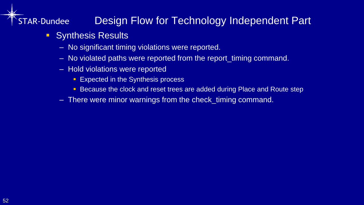
▪ Synthesis Results
– No significant timing violations were reported.
– No violated paths were reported from the report_timing command.
– Hold violations were reported
▪ Expected in the Synthesis process
▪ Because the clock and reset trees are added during Place and Route step
– There were minor warnings from the check_timing command.
52

Design Flow for Technology Independent Part
▪ Formality Run
– After synthesis
– Logic equivalence checks performed
– To ensure correctness of design
▪ Comparison completed without errors
– 277331 matched points
– 34 unmatched points
▪ All in the reference and considered as acceptable
▪ Because a lot of registers in the reference were removed during synthesis
– they are either constant or never read
– they have no counterpart in the implementation
53
Chip Area Estimation
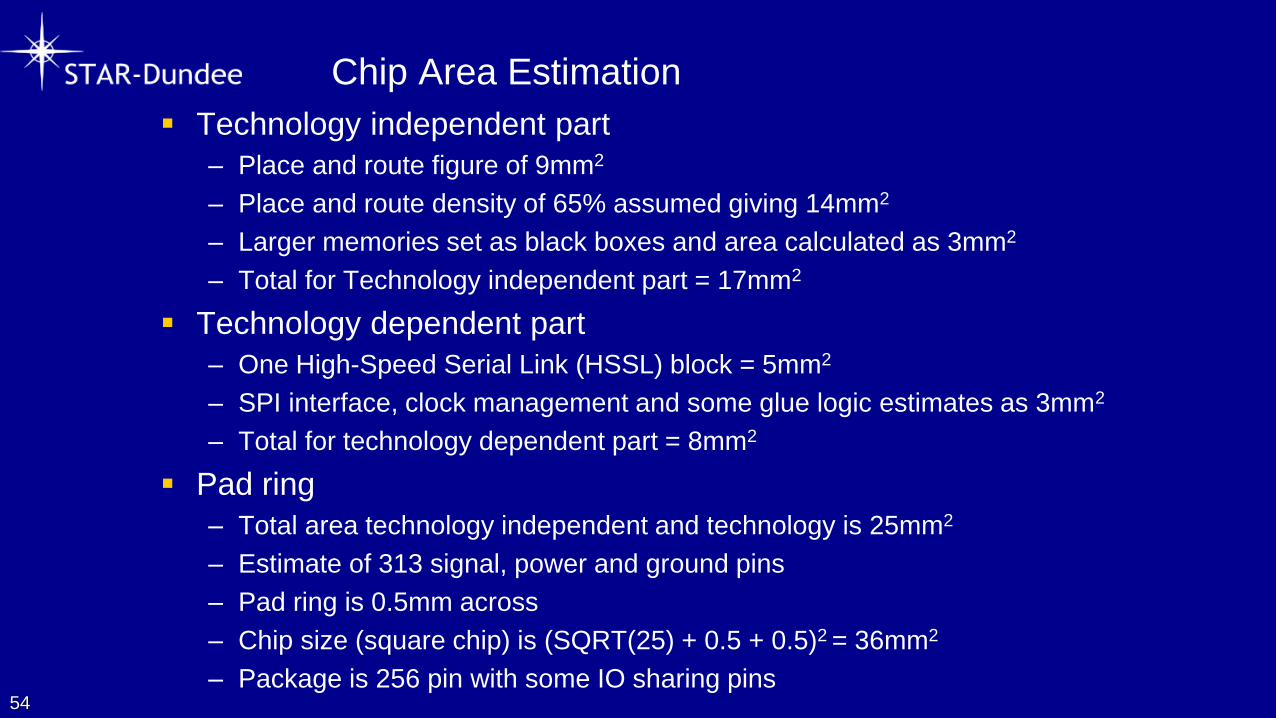
▪ Technology independent part
– Place and route figure of 9mm2
– Place and route density of 65% assumed giving 14mm2
– Larger memories set as black boxes and area calculated as 3mm2
– Total for Technology independent part = 17mm2
▪ Technology dependent part
– One High-Speed Serial Link (HSSL) block = 5mm2
– SPI interface, clock management and some glue logic estimates as 3mm2
– Total for technology dependent part = 8mm2
▪ Pad ring
– Total area technology independent and technology is 25mm2
– Estimate of 313 signal, power and ground pins
– Pad ring is 0.5mm across
– Chip size (square chip) is (SQRT(25) + 0.5 + 0.5)2 = 36mm2
– Package is 256 pin with some IO sharing pins 54

SpaceFibre Interface Chip
Conclusions
Steve Parkes (CTO) STAR-Dundee Ltd.
Study Achievements
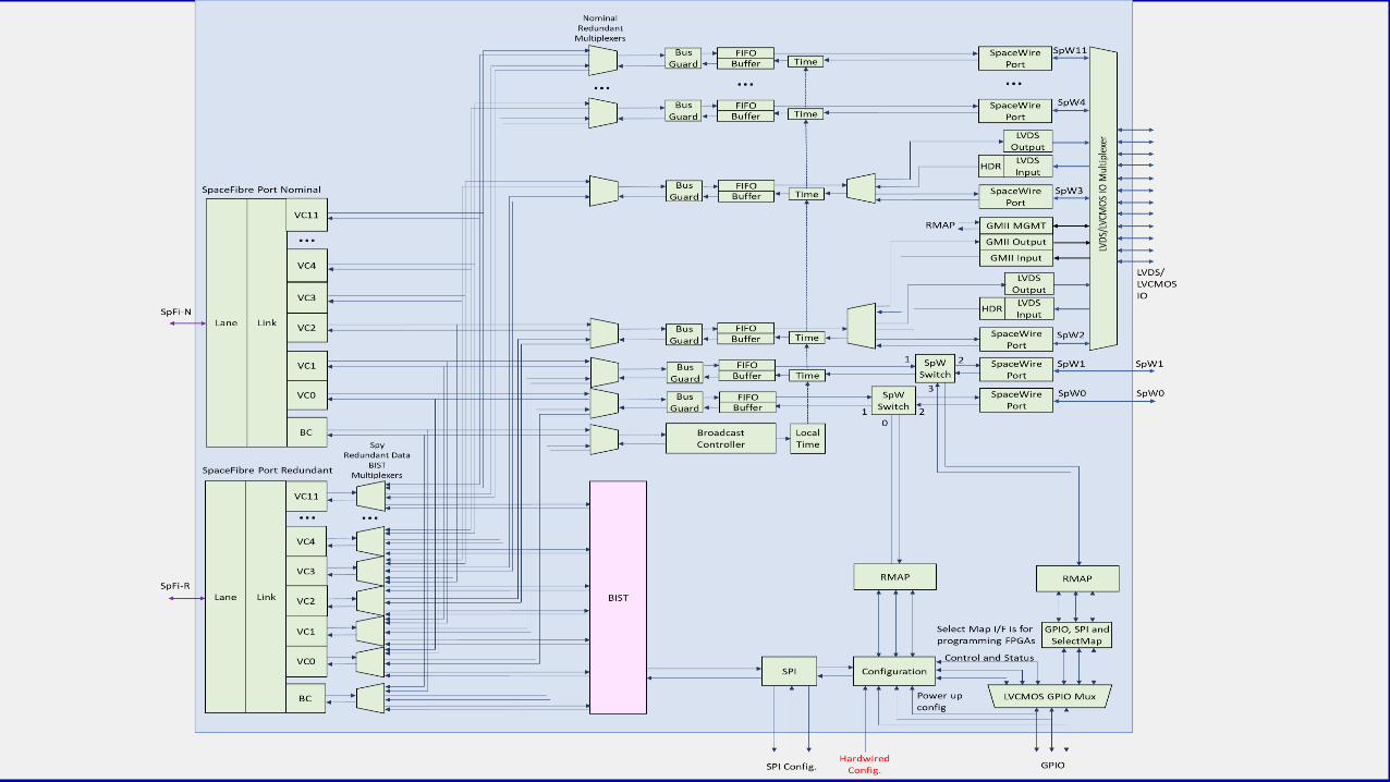
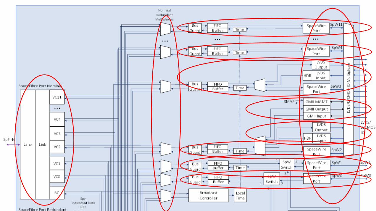
▪ A SpaceFibre interface chip has been specified, designed, verified in
simulation, and validated in a hardware prototype
– Two SpaceFibre ports (nominal and redundant)
▪ Operating at data rates of 1, 2.5, 3.125 and 6.25 Gbit/s baud rate
– Highly configurable bridging modes including:
▪ SpaceWire bridging to up to 12 SpaceWire ports
– Each mapping onto a separate SpaceFibre virtual channel
– Operating at up to 200 Mbit/s
▪ Parallel bridging to up to two parallel ports
– Independently configured as inputs or outputs
– Operate at 2.5 Gbit/s each using a 78 MHz DDR clock (higher data rates also possible)
– Two SpaceWire ports available when both parallel ports are used
▪ Seven when just one parallel port is used.
▪ Gigabit Ethernet bridging
– With SpaceFibre Interface Chip acting as GMII PHY and operating at 1GbE speeds
– GMII interface is configured in place of one of the Parallel ports.
56

Study Achievements
– 32-bit GPIO interface
▪ With multiple operating modes including
– Data input/output
– I2C and SPI interfaces
– System time
– Time-codes
– Chip status
– Supports remote FPGA programming over SpaceFibre
▪ Using a JTAG or SelectMAP programming interface to the FPGA.
– Configuration of the SpaceFibre Interface Chip itself
▪ Over SpaceFibre, SpaceWire and local SPI interface
▪ Initial configuration setting via the GPIO port
– Designed to fit in a package with around 256 pins
– SpaceFibre Interface Chip specified, designed, verified in simulation and validated in
FPGA-based, hardware prototype
– Feasibility of transfer to radiation tolerant ASIC technology evaluated and confirmed
through initial synthesis and formality check57

Summary and Conclusions
▪ SpaceFibre Interface Chip
– Extremely versatile and high-performance SpaceFibre Interface Chip
▪ Designed
▪ Implemented in VHDL
▪ Verified through simulation
▪ Validated in prototype hardware
– Meets the requirements defined by ESA, Airbus, RUAG Space and STAR-Dundee
▪ SpaceFibre Interface Chip test results were
– Compared against the chip specification in a verification matrix
– Total of 179 specifications
– Four deleted because they were no longer relevant
– Nine were not implemented, with agreement from ESA
– Of the remaining 166 specifications
▪ 6 were partly implemented
▪ 160 fully implemented and verified using a mixture of hardware testing and simulation
58
Summary and Conclusions
▪ Feasibility of migrating this design to a radiation tolerant ASIC
– Assessed with an initial synthesis in STM 65nm technology
– Results of this synthesis were successful
– Formality check also performed with success
▪ Expected chip size was calculated
– 36mm2
▪ Outline plan provided moving towards ASIC implementation
59