Embed Size (px)
Citation preview
U.S. Government work not protected by U.S. copyright 1
SpaceCube v2.0 Space Flight Hybrid Reconfigurable Data Processing System
David Petrick, Alessandro Geist, Dennis Albaijes, Milton Davis, Pietro Sparacino, Gary Crum, Robin Ripley, Jonathan Boblitt, and Thomas Flatley
NASA Goddard Space Flight
Greenbelt, MD 20771 [email protected]
Abstract—This paper details the design architecture, design methodology, and the advantages of the SpaceCube v2.0 high performance data processing system for space applications. The purpose in building the SpaceCube v2.0 system is to create a superior high performance, reconfigurable, hybrid data processing system that can be used in a multitude of applications including those that require a radiation hardened and reliable solution. The SpaceCube v2.0 system leverages seven years of board design, avionics systems design, and space flight application experiences. This paper shows how SpaceCube v2.0 solves the increasing computing demands of space data processing applications that cannot be attained with a standalone processor approach. The main objective during the design stage is to find a good system balance between power, size, reliability, cost, and data processing capability. These design variables directly impact each other, and it is important to understand how to achieve a suitable balance. This paper will detail how these critical design factors were managed including the construction of an Engineering Model for an experiment on the International Space Station to test out design concepts. We will describe the designs for the processor card, power card, backplane, and a mission unique interface card. The mechanical design for the box will also be detailed since it is critical in meeting the stringent thermal and structural requirements imposed by the processing system. In addition, the mechanical design uses advanced thermal conduction techniques to solve the internal thermal challenges. The SpaceCube v2.0 processing system is based on an extended version of the 3U cPCI standard form factor where each card is 190mm x 100mm in size. The typical power draw of the processor card is 8 to 10W and scales with application complexity. The SpaceCube v2.0 data processing card features two Xilinx Virtex-5 QV Field Programmable Gate Arrays (FPGA), eight memory modules, a monitor FPGA with analog monitoring, Ethernet, configurable interconnect to the Xilinx FPGAs including gigabit transceivers, and the necessary voltage regulation. The processor board uses a back-to-back design methodology for common parts that maximizes the board real estate available. This paper will show how to meet the IPC 6012B Class 3/A standard with a 22-layer board that has two column grid array devices with 1.0mm pitch. All layout trades such as stack-up options, via selection, and FPGA signal breakout will be discussed with feature size results. The overall board design process will be discussed including parts selection, circuit design, proper signal termination, layout placement and route planning, signal integrity design and verification, and power integrity results. The radiation mitigation techniques will also be detailed including configuration scrubbing options, Xilinx circuit mitigation and FPGA functional monitoring, and memory protection.
Finally, this paper will describe how this system is being used to solve the extreme challenges of a robotic satellite servicing mission where typical space-rated processors are not sufficient enough to meet the intensive data processing requirements. The SpaceCube v2.0 is the main payload control computer and is required to control critical subsystems such as autonomous rendezvous and docking using a suite of vision sensors and object avoidance when controlling two robotic arms. For this application three SpaceCube processing systems are required, each with two processor cards.
TABLE OF CONTENTS
1. INTRODUCTION ............................................... 1 2. SYSTEM DESIGN METHODOLOGY ................... 3 3. PROCESSOR CARD DESIGN .............................. 3 4. POWER CARD DESIGN ................................... 12 5. BACKPLANE DESIGN ..................................... 13 6. MECHANICAL/THERMAL DESIGN ................. 13 7. MISSION CASE STUDY ................................... 16 8. CONCLUSIONS ............................................... 17 8. FUTURE WORK ............................................. 18 REFERENCES .................................................... 18 BIOGRAPHY ...................................................... 19
1. INTRODUCTION SpaceCube is a family of Field Programmable Gate Array (FPGA) based on-board science data processing systems developed at the NASA Goddard Space Flight Center (GSFC) [1]. The goal of the SpaceCube program is to provide 10x to 100x improvements in on-board computing power while lowering relative power consumption and cost. SpaceCube is based on the Xilinx Virtex family of FPGAs, which include processor, FPGA and digital signal processing (DSP) resources. These processing elements are leveraged to produce a hybrid science data processing platform that accelerates the execution of algorithms by distributing computational functions to the most suitable elements. This approach enables the implementation of complex on-board functions that were previously limited to ground based systems, such as on-board product generation, data reduction, calibration, classification, event/feature detection, data mining and real-time autonomous operations. The system is fully reconfigurable in flight, including data parameters, software and FPGA logic, through either ground
2
commanding or autonomously in response to detected events/features in the instrument data stream.
A. Background
The SpaceCube processing system at GSFC was started in 2006 funded by the Internal Research and Development (IRAD) program [2]. A series of internal prototype demonstrations to NASA officials showcased the computational power and its inherent reconfigurable advantages over typical space processors. NASA recognized the clear potential of the technology, and provided the funding needed to increase the Technology Readiness Level (TRL) for space flight applications. Specifically, the Hubble Space Telescope Servicing Mission 4 management team employed the SpaceCube as the main avionics for an experimental payload called Relative Navigation Sensors (RNS) [1, 3, 6, 8].
The version of the SpaceCube that was initially developed in the 2006-2009 timeframe is known as SpaceCube v1.0. Following the success of the RNS mission, a v1.0 system was added to an International Space Station experimental payload to study long term effects of radiation [1, 5, 10, 17]. SpaceCube v1.0 is also the main avionics system to control two follow-on ISS experiments for the Department of Defense (DoD) [7, 11].
SpaceCube v1.0 was based on the Xilinx Virtex 4 series of FPGAs. SpaceCube v1.5 was designed with the Virtex 5 series of FPGAs, but remained backward compatible with the v1.0 custom form factor. This system was flown in space in 2011 on an advanced DoD-funded sounding rocket project that used a SpaceCube v1.5 processing system to collect high speed data from cameras, navigation instruments, and monitor system health. All of this data was recorded to SATA-II memory drives utilizing the Xilinx GTX gigabit transceivers, and simultaneously downlinked real-time to ground operators [12, 17]
SpaceCube v1.5 was used to bridge the technology from SpaceCube v1.0 to SpaceCube v2.0. The design and use of the SpaceCube v2.0 processing system will be the focus of this paper. SpaceCube v2.0 was funded by NASA’s Earth Science Technology Office (ESTO) and Satellite Servicing Capabilities Office (SSCO).
B. Current Space Processing Challenges
There is a growing need for higher performance processing systems for space. Instrument precision and speed capabilities are rapidly evolving which levies tougher electrical interfacing and data bandwidth requirements on the computing node of the system. In addition, on-board processing of the data products, in some cases in real-time, is now a common requirement.
On-board processing improves system efficiency and functionality in two areas. First, by allowing the spacecraft
to preprocess data products on board, a smaller or compressed data volume per data set can be sent to ground, which increases the amount of time an instrument can be turned on and collecting data. It is typical for high data rate science instruments to constrain their data collection to 10-20% of the mission time to fit within the limited downlink bandwidth. This problem continues to grow as instrument capabilities increase. Second, it enables applications on board the spacecraft to make autonomous decisions based on the processed data products. This ability opens up a much more challenging range of mission objectives that can be targeted for space applications.
Typical space processing systems generally consist of a single radiation hardened processor such as the BAE RAD750, Aeroflex LEON3FT, BroadReach BRE440, or General Dynamics ColdFire which all deliver less than 300 DMIPS. These standard processing systems are very good at providing general services such as Command and Data Handling (C&DH), Guidance and Navigation Control (G&NC), and simple instrument control. These processing systems are not good candidates for applications that require implementing fast computations of complex algorithms on a high bandwidth or large volume data source.
Another common component found in typical space processing systems is the anti-fuse FPGA, which generally have very good radiation immunity. The corresponding circuit board and FPGA architectures are designed for a set of very specific mission requirements. However, these architectures are very hard to design and intrinsically expensive to modify such that they are adaptable to multiple missions, dynamic functional requirements, or new post-launch mission objectives or corrections.
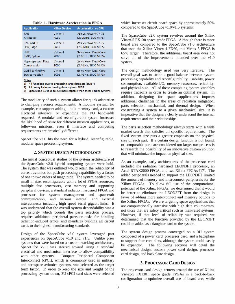
A new approach is needed to meet the increasing challenges required by space processing systems. A hybrid computing system that combines multiple processors, reconfigurable FPGAs, flexible interface options, with a modular architecture is the solution that will bridge the gap between today’s avionics requirements and yesterday’s typical stand-alone, sequential processing architecture. A hybrid computing architecture is able to retain the function of a multi-purpose computer that runs typical C&DH and G&NC. However, in addition to these types of tasks, it has the advantage of supporting computationally complex tasks that require FPGA co-processors to handle complex mathematical operators such as Fast Fourier Transforms (FFT), matrix manipulation, and parallel floating point operations, or implementing advanced interfaces such as CameraLink, Spacewire, and gigabit Ethernet, or support the implementation of a custom interface. Samples of our hardware acceleration accomplishments in FPGA are shown in Table 1, which shows that it is possible to converge or surpass “lab computer” performance [14, 15, 16].
3
Table 1 - Hardware Acceleration in FPGA
The modularity of such a system allows for quick adaptation to changing avionics requirements. A modular system, for example, can support adding a bulk memory card, a custom electrical interface, or expanding the I/O bandwidth required. A modular and reconfigurable system increases the likelihood of reuse for different mission applications, or follow-on missions, even if interface and computing requirements are drastically different.
SpaceCube v2.0 fits the need for a hybrid, reconfigurable, modular space processing system.
2. SYSTEM DESIGN METHODOLOGY The initial conceptual studies of the system architecture of the SpaceCube v2.0 hybrid computing system were bold. The system that was outlined would retain the reliability of current avionics but push processing capabilities by a factor of one to two orders of magnitude. The system needed to be small in size, reconfigurable with a lot of FPGA resources, multiple fast processors, vast memory and supporting peripheral devices, a standard radiation hardened FPGA and processor for system management and spacecraft communication, and various internal and external interconnects including high speed serial gigabit links. It was understood that the overall system dependability was a top priority which bounds the parts selection process, requires additional peripheral parts or tasks for handling radiation-induced errors, and mandates building all circuit cards to the highest manufacturing standards.
Design of the SpaceCube v2.0 system leveraged past experiences on SpaceCube v1.0 and v1.5. Unlike prior systems that were based on a custom stacking architecture, SpaceCube v2.0 was steered toward using a standard electrical and mechanical interface to allow compatibility with other systems. Compact Peripheral Component Interconnect (cPCI), which is commonly used in military and aerospace avionics systems, was selected as the target form factor. In order to keep the size and weight of the processing system down, 3U cPCI card sizes were selected
which increases circuit board space by approximately 50% compared to the SpaceCube v1.0/v1.5 systems.
The SpaceCube v2.0 system revolves around the Xilinx Virtex-5 FX130 space grade FPGA. Although there is more board area compared to the SpaceCube v1.0 architecture that used the Xilinx Virtex-4 FX60, this Virtex-5 FPGA is 65% larger. Therefore, the additional board area does not solve all of the improvements intended over the v1.0 system.
The design methodology used was very iterative. The overall goal was to strike a good balance between system processing capability and reconfigurability, usability, power consumption, available I/O, memory resources, reliability, and physical size. All of these competing system variables require tradeoffs in order to create an optimal system. In addition, designing for space applications imposes additional challenges in the areas of radiation mitigation, parts selection, mechanical, and thermal design. When constraining a system to a given mechanical size, it is imperative that the designers clearly understand the internal requirements and their relationships.
The parts selection methodology always starts with a wide market search that satisfies all specific requirements. The fixed system size puts a greater emphasis on the physical size of each part. If a certain design function is not found, or comparable parts are considered too large, our process is to research the possibility of an innovative custom solution that will minimize the impact on physical size.
As an example, early architectures of the processor card included the radiation hardened LEON3FT processor, an Actel RTAX2000 FPGA, and two Xilinx FPGAs [17]. The added peripherals needed to support the LEON3FT limited the amount of memory and interconnect peripherals for the Xilinx FPGAs. To allow full use of the computational potential of the Xilinx FPGAs, we determined that it would be better to eliminate the LEON3FT from the design in favor of adding more interconnect and memory options to the Xilinx FPGAs. We are targeting space applications that are computationally intensive with high data volume/rates, not those that are safety critical such as man-rated systems. However, if that level of reliability was required, we determined that the function provided by the LEON3FT could be added as a daughter card to the system.
The system design process converged on a 3U system composed of a power card, processor card, and a backplane to support four card slots, although the system could easily be expanded. The following sections will detail the mechanical design, custom power card design, processor card design, and backplane design.
3. PROCESSOR CARD DESIGN The processor card design centers around the use of Xilinx Virtex-5 FX130T space grade FPGAs in a back-to-back configuration to optimize overall use of board area while
4
maximizing computing power. This method was first used on the SpaceCube v1.0 processor board that features two Virtex-4 FX60 FPGAs. Multiple embedded PowerPC440 (commercial device only) or MicroBlaze processors can be used to satisfy processing requirements. When necessary, the use of the FPGAs enables parallel hardware acceleration of applications. The resulting multi-processor platform is inherently reconfigurable, providing application designers a flexible system that enables quick development. A reconfigurable system also gives mission operations the ability to dynamically alter mission objectives post-launch. The goal of the processor card was to find a balance of design parameters that would appeal to a wide array of potential mission applications.
We also required that the processor card design would support multiple serial gigabit links using the Xilinx GTX transceivers. We demonstrated their use in space on SpaceCube v1.5 by implementing SATA-II interfaces as part of a sounding rocket application. However, SpaceCube v1.5 was built mostly with commercial devices that could not be used in the SpaceCube v2.0 design.
In order to meet all of the desired objectives with the SpaceCube v2.0 processing system, we decided to build an Engineering Model to test various new circuit techniques. Through the evaluation of the engineering model, we converged on design decisions for the flight model.
A. Engineering Model
The purpose of this revision was to design and test multiple electrical options for handling the Xilinx Virtex-5 on a space flight board. We were mostly concerned with the parts selection and circuit designs to support the system clocking, GTX power and clocking, Xilinx power delivery and decoupling, peripheral termination schemes, Xilinx configuration solutions, and external connectors. Another objective of the Engineering Model (EM) was to meet IPC-6012B Class 3/A Printed Wiring Board (PWB) manufacturing specification, which is typically required by NASA for space systems. Due to the number of circuits, the EM was designed on a 6U board, which is more than double the size of a 3U board. However, the majority of the main circuitry was constrained to a 3U area to prepare for the upcoming challenges of the flight board design.
The EM board has three Xilinx Virtex-5 FPGAs, which results in roughly 6x the digital logic resources of the SpaceCube v1.0 processor card. Each FPGA footprint supports either the commercial grade or space grade FX130 FPGA. The unique use of the Xilinx Virtex-5 FPGAs and supporting circuitry in a back-to-back fashion that allows for maximum use of board real estate. One of the three FPGAs is the main board controller. This FPGA has radiation hardened SRAM, DDR SDRAM, a custom 16-channel Analog to Digital Converter (ADC), two NAND flash memories, and 10/100 Ethernet. It is configured from a radiation-hardened PROM via Master SelectMap and is capable of self configuration repair. It is responsible for
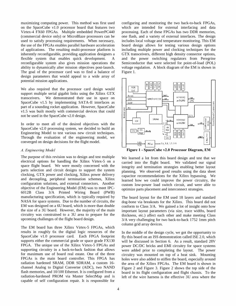
configuring and monitoring the two back-to-back FPGAs, which are intended for external interfacing and data processing. Each of these FPGAs has two DDR memories, one flash, and a variety of external interfaces. The design includes local voltage and temperature monitoring. This EM board design allows for testing various design options including multiple power and clocking techniques for the GTX transceivers, different high density connector options, and the power switching regulators from Peregrine Semiconductor that were selected for point-of-load (POL) voltage regulation. A block diagram of the EM is shown in Figure 1.
Figure 1 - SpaceCube v2.0 Processor Diagram, EM
We learned a lot from this board design and test that we carried into the flight board. We validated our signal integrity and termination strategies enabling better layout planning. We observed good results using the data sheet capacitor recommendations for the Xilinx bypassing. We learned how we could improve the power circuitry, the custom low-power load switch circuit, and were able to optimize parts placement and interconnect strategies.
The board layout for the EM used 18 layers and standard dog-bone via breakouts for the Xilinx. This board did not conform to Class 3/A. We gained a lot of insight onto how important layout parameters (via size, trace widths, board thickness, etc.) affect each other and make meeting Class 3/A very challenging for two back-to-back 1752 1mm pitch column grid array devices.
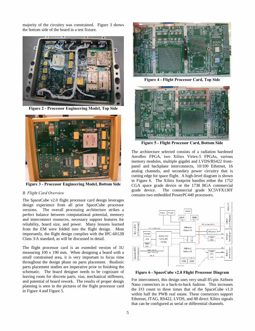
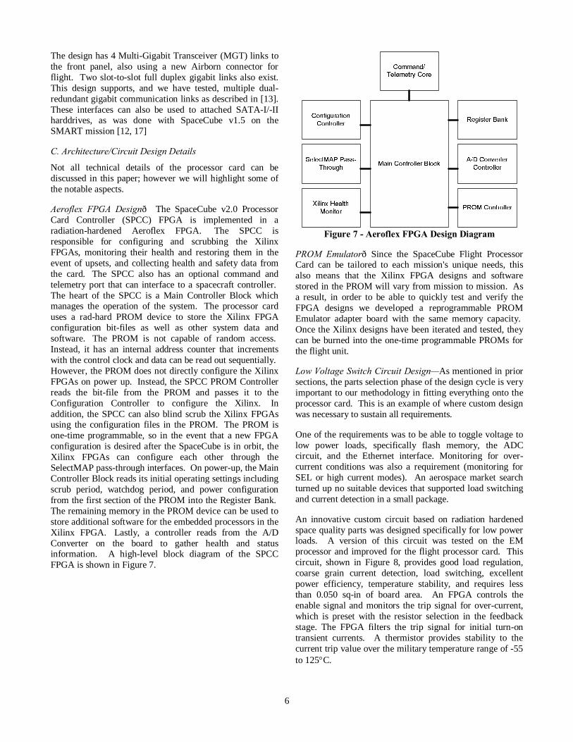
In the middle of the design cycle, we got the opportunity to fly this board on an ISS demonstration called ISE 2.0, which will be discussed in Section 6. As a result, standard 28V power DC/DC bricks and EMI circuitry for space systems were added prior to completing the layout. The power circuitry was mounted on top of a heat sink. Mounting holes were also added to stiffen the board, especially around the area of the Xilinx FPGAs. The EM board is shown in Figure 2 and Figure 3. Figure 2 shows the top side of the board in its flight configuration and flight chassis. To the left of the wire harness is the effective 3U area where the
5
majority of the circuitry was constrained. Figure 3 shows the bottom side of the board in a test fixture.
Figure 2 - Processor Engineering Model, Top Side
Figure 3 - Processor Engineering Model, Bottom Side
B. Flight Card Overview
The SpaceCube v2.0 flight processor card design leverages design experience from all prior SpaceCube processor versions. The overall processing architecture strikes a perfect balance between computational potential, memory and interconnect resources, necessary support features for reliability, board size, and power. Many lessons learned from the EM were folded into the flight design. Most importantly, the flight design complies with the IPC-6012B Class 3/A standard, as will be discussed in detail.
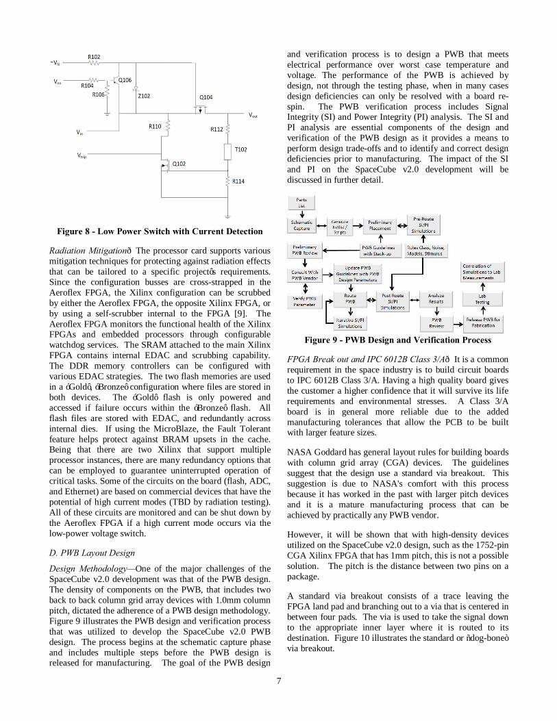
The flight processor card is an extended version of 3U measuring 100 x 190 mm. When designing a board with a small constrained area, it is very important to focus time throughout the design phase on parts placement. Realistic parts placement studies are imperative prior to finishing the schematic. The board designer needs to be cognizant of leaving room for discrete parts, vias, mechanical stiffeners, and potential of board rework. The results of proper design planning is seen in the pictures of the flight processor card in Figure 4 and Figure 5.
Figure 4 - Flight Processor Card, Top Side
Figure 5 - Flight Processor Card, Bottom Side
The architecture selected consists of a radiation hardened Aeroflex FPGA, two Xilinx Virtex-5 FPGAs, various memory modules, multiple gigabit and LVDS/RS422 front-panel and backplane interconnects, 10/100 Ethernet, 16 analog channels, and secondary power circuitry that is cutting edge for space flight. A high-level diagram is shown in Figure 6. The Xilinx footprint handles either the 1752 CGA space grade device or the 1738 BGA commercial grade device. The commercial grade XC5VFX130T contains two embedded PowerPC440 processors.
Figure 6 - SpaceCube v2.0 Flight Processor Diagram
For interconnect, this design uses very small 85-pin Airborn Nano connectors in a back-to-back fashion. This increases the I/O count to three times that of the SpaceCube v1.0 within half the PWB real estate. These connectors support Ethernet, JTAG, RS422, LVDS, and 88 direct Xilinx signals that can be configured as serial or differential channels.
6
The design has 4 Multi-Gigabit Transceiver (MGT) links to the front panel, also using a new Airborn connector for flight. Two slot-to-slot full duplex gigabit links also exist. This design supports, and we have tested, multiple dual-redundant gigabit communication links as described in [13]. These interfaces can also be used to attached SATA-I/-II harddrives, as was done with SpaceCube v1.5 on the SMART mission [12, 17]
C. Architecture/Circuit Design Details
Not all technical details of the processor card can be discussed in this paper; however we will highlight some of the notable aspects.
Aeroflex FPGA Design— The SpaceCube v2.0 Processor Card Controller (SPCC) FPGA is implemented in a radiation-hardened Aeroflex FPGA. The SPCC is responsible for configuring and scrubbing the Xilinx FPGAs, monitoring their health and restoring them in the event of upsets, and collecting health and safety data from the card. The SPCC also has an optional command and telemetry port that can interface to a spacecraft controller. The heart of the SPCC is a Main Controller Block which manages the operation of the system. The processor card uses a rad-hard PROM device to store the Xilinx FPGA configuration bit-files as well as other system data and software. The PROM is not capable of random access. Instead, it has an internal address counter that increments with the control clock and data can be read out sequentially. However, the PROM does not directly configure the Xilinx FPGAs on power up. Instead, the SPCC PROM Controller reads the bit-file from the PROM and passes it to the Configuration Controller to configure the Xilinx. In addition, the SPCC can also blind scrub the Xilinx FPGAs using the configuration files in the PROM. The PROM is one-time programmable, so in the event that a new FPGA configuration is desired after the SpaceCube is in orbit, the Xilinx FPGAs can configure each other through the SelectMAP pass-through interfaces. On power-up, the Main Controller Block reads its initial operating settings including scrub period, watchdog period, and power configuration from the first section of the PROM into the Register Bank. The remaining memory in the PROM device can be used to store additional software for the embedded processors in the Xilinx FPGA. Lastly, a controller reads from the A/D Converter on the board to gather health and status information. A high-level block diagram of the SPCC FPGA is shown in Figure 7.
Figure 7 - Aeroflex FPGA Design Diagram
PROM Emulator—Since the SpaceCube Flight Processor Card can be tailored to each mission's unique needs, this also means that the Xilinx FPGA designs and software stored in the PROM will vary from mission to mission. As a result, in order to be able to quickly test and verify the FPGA designs we developed a reprogrammable PROM Emulator adapter board with the same memory capacity. Once the Xilinx designs have been iterated and tested, they can be burned into the one-time programmable PROMs for the flight unit.
Low Voltage Switch Circuit Design—As mentioned in prior sections, the parts selection phase of the design cycle is very important to our methodology in fitting everything onto the processor card. This is an example of where custom design was necessary to sustain all requirements.
One of the requirements was to be able to toggle voltage to low power loads, specifically flash memory, the ADC circuit, and the Ethernet interface. Monitoring for over-current conditions was also a requirement (monitoring for SEL or high current modes). An aerospace market search turned up no suitable devices that supported load switching and current detection in a small package.
An innovative custom circuit based on radiation hardened space quality parts was designed specifically for low power loads. A version of this circuit was tested on the EM processor and improved for the flight processor card. This circuit, shown in Figure 8, provides good load regulation, coarse grain current detection, load switching, excellent power efficiency, temperature stability, and requires less than 0.050 sq-in of board area. An FPGA controls the enable signal and monitors the trip signal for over-current, which is preset with the resistor selection in the feedback stage. The FPGA filters the trip signal for initial turn-on transient currents. A thermistor provides stability to the current trip value over the military temperature range of -55 to 125°C.
7
Figure 8 - Low Power Switch with Current Detection
Radiation Mitigation—The processor card supports various mitigation techniques for protecting against radiation effects that can be tailored to a specific project’s requirements. Since the configuration busses are cross-strapped in the Aeroflex FPGA, the Xilinx configuration can be scrubbed by either the Aeroflex FPGA, the opposite Xilinx FPGA, or by using a self-scrubber internal to the FPGA [9]. The Aeroflex FPGA monitors the functional health of the Xilinx FPGAs and embedded processors through configurable watchdog services. The SRAM attached to the main Xilinx FPGA contains internal EDAC and scrubbing capability. The DDR memory controllers can be configured with various EDAC strategies. The two flash memories are used in a ‘Gold’, ‘Bronze’ configuration where files are stored in both devices. The ‘Gold’ flash is only powered and accessed if failure occurs within the ‘Bronze’ flash. All flash files are stored with EDAC, and redundantly across internal dies. If using the MicroBlaze, the Fault Tolerant feature helps protect against BRAM upsets in the cache. Being that there are two Xilinx that support multiple processor instances, there are many redundancy options that can be employed to guarantee uninterrupted operation of critical tasks. Some of the circuits on the board (flash, ADC, and Ethernet) are based on commercial devices that have the potential of high current modes (TBD by radiation testing). All of these circuits are monitored and can be shut down by the Aeroflex FPGA if a high current mode occurs via the low-power voltage switch.
D. PWB Layout Design
Design Methodology—One of the major challenges of the SpaceCube v2.0 development was that of the PWB design. The density of components on the PWB, that includes two back to back column grid array devices with 1.0mm column pitch, dictated the adherence of a PWB design methodology. Figure 9 illustrates the PWB design and verification process that was utilized to develop the SpaceCube v2.0 PWB design. The process begins at the schematic capture phase and includes multiple steps before the PWB design is released for manufacturing. The goal of the PWB design
and verification process is to design a PWB that meets electrical performance over worst case temperature and voltage. The performance of the PWB is achieved by design, not through the testing phase, when in many cases design deficiencies can only be resolved with a board re-spin. The PWB verification process includes Signal Integrity (SI) and Power Integrity (PI) analysis. The SI and PI analysis are essential components of the design and verification of the PWB design as it provides a means to perform design trade-offs and to identify and correct design deficiencies prior to manufacturing. The impact of the SI and PI on the SpaceCube v2.0 development will be discussed in further detail.
Figure 9 - PWB Design and Verification Process
FPGA Break out and IPC 6012B Class 3/A—It is a common requirement in the space industry is to build circuit boards to IPC 6012B Class 3/A. Having a high quality board gives the customer a higher confidence that it will survive its life requirements and environmental stresses. A Class 3/A board is in general more reliable due to the added manufacturing tolerances that allow the PCB to be built with larger feature sizes.
NASA Goddard has general layout rules for building boards with column grid array (CGA) devices. The guidelines suggest that the design use a standard via breakout. This suggestion is due to NASA's comfort with this process because it has worked in the past with larger pitch devices and it is a mature manufacturing process that can be achieved by practically any PWB vendor.
However, it will be shown that with high-density devices utilized on the SpaceCube v2.0 design, such as the 1752-pin CGA Xilinx FPGA that has 1mm pitch, this is not a possible solution. The pitch is the distance between two pins on a package.
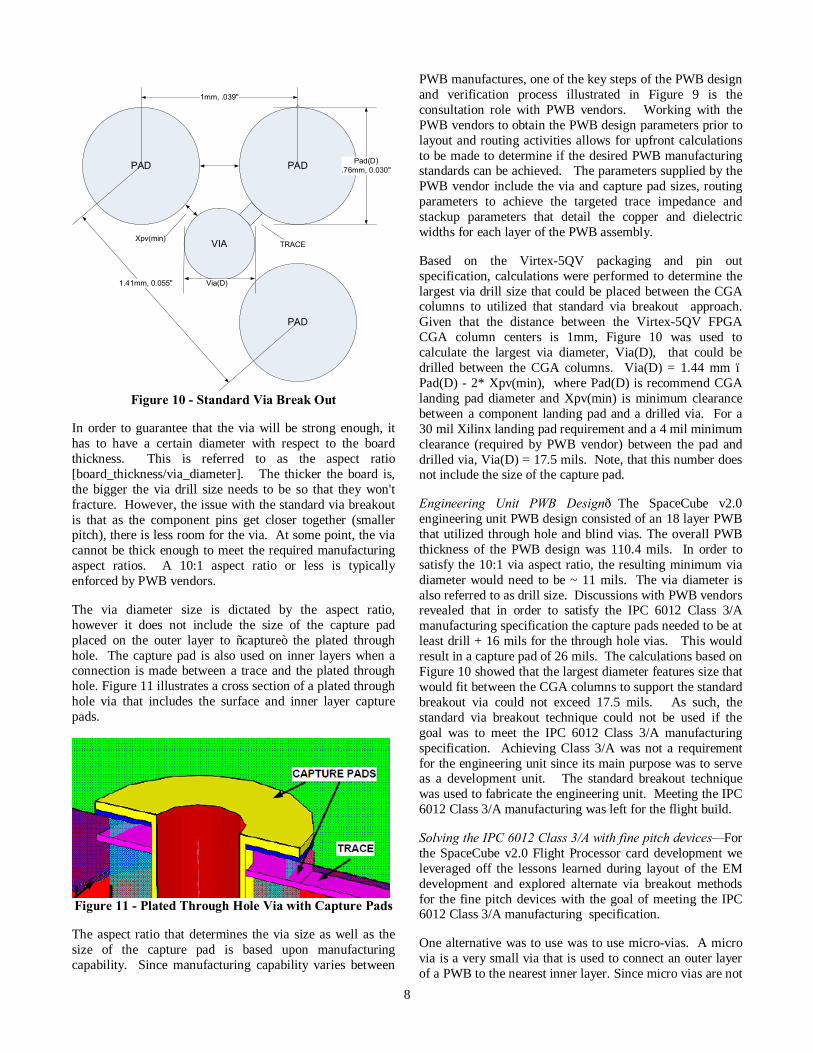
A standard via breakout consists of a trace leaving the FPGA land pad and branching out to a via that is centered in between four pads. The via is used to take the signal down to the appropriate inner layer where it is routed to its destination. Figure 10 illustrates the standard or “dog-bone” via breakout.
8
PAD
VIA
PAD
PAD
1mm, .039"
1.41mm, 0.055"
Pad(D).76mm, 0.030"
Xpv(min)TRACE
Via(D)
Figure 10 - Standard Via Break Out
In order to guarantee that the via will be strong enough, it has to have a certain diameter with respect to the board thickness. This is referred to as the aspect ratio [board_thickness/via_diameter]. The thicker the board is, the bigger the via drill size needs to be so that they won't fracture. However, the issue with the standard via breakout is that as the component pins get closer together (smaller pitch), there is less room for the via. At some point, the via cannot be thick enough to meet the required manufacturing aspect ratios. A 10:1 aspect ratio or less is typically enforced by PWB vendors.
The via diameter size is dictated by the aspect ratio, however it does not include the size of the capture pad placed on the outer layer to “capture” the plated through hole. The capture pad is also used on inner layers when a connection is made between a trace and the plated through hole. Figure 11 illustrates a cross section of a plated through hole via that includes the surface and inner layer capture pads.
Figure 11 - Plated Through Hole Via with Capture Pads
The aspect ratio that determines the via size as well as the size of the capture pad is based upon manufacturing capability. Since manufacturing capability varies between
PWB manufactures, one of the key steps of the PWB design and verification process illustrated in Figure 9 is the consultation role with PWB vendors. Working with the PWB vendors to obtain the PWB design parameters prior to layout and routing activities allows for upfront calculations to be made to determine if the desired PWB manufacturing standards can be achieved. The parameters supplied by the PWB vendor include the via and capture pad sizes, routing parameters to achieve the targeted trace impedance and stackup parameters that detail the copper and dielectric widths for each layer of the PWB assembly.
Based on the Virtex-5QV packaging and pin out specification, calculations were performed to determine the largest via drill size that could be placed between the CGA columns to utilized that standard via breakout approach. Given that the distance between the Virtex-5QV FPGA CGA column centers is 1mm, Figure 10 was used to calculate the largest via diameter, Via(D), that could be drilled between the CGA columns. Via(D) = 1.44 mm – Pad(D) - 2* Xpv(min), where Pad(D) is recommend CGA landing pad diameter and Xpv(min) is minimum clearance between a component landing pad and a drilled via. For a 30 mil Xilinx landing pad requirement and a 4 mil minimum clearance (required by PWB vendor) between the pad and drilled via, Via(D) = 17.5 mils. Note, that this number does not include the size of the capture pad.
Engineering Unit PWB Design—The SpaceCube v2.0 engineering unit PWB design consisted of an 18 layer PWB that utilized through hole and blind vias. The overall PWB thickness of the PWB design was 110.4 mils. In order to satisfy the 10:1 via aspect ratio, the resulting minimum via diameter would need to be ~ 11 mils. The via diameter is also referred to as drill size. Discussions with PWB vendors revealed that in order to satisfy the IPC 6012 Class 3/A manufacturing specification the capture pads needed to be at least drill + 16 mils for the through hole vias. This would result in a capture pad of 26 mils. The calculations based on Figure 10 showed that the largest diameter features size that would fit between the CGA columns to support the standard breakout via could not exceed 17.5 mils. As such, the standard via breakout technique could not be used if the goal was to meet the IPC 6012 Class 3/A manufacturing specification. Achieving Class 3/A was not a requirement for the engineering unit since its main purpose was to serve as a development unit. The standard breakout technique was used to fabricate the engineering unit. Meeting the IPC 6012 Class 3/A manufacturing was left for the flight build.
Solving the IPC 6012 Class 3/A with fine pitch devices—For the SpaceCube v2.0 Flight Processor card development we leveraged off the lessons learned during layout of the EM development and explored alternate via breakout methods for the fine pitch devices with the goal of meeting the IPC 6012 Class 3/A manufacturing specification.
One alternative was to use was to use micro-vias. A micro via is a very small via that is used to connect an outer layer of a PWB to the nearest inner layer. Since micro vias are not
9
drilled through the entire PWB, they are not constrained by the 10:1 aspect ratio. The overall PWB thickness of the Engineering Unit would support a 7 mil micro-via with an additional 7 mil required for the capture pad. The resulting 14 mil pad could fit between the CGA pads in order to meet the Class 3/A manufacturing specifications.
The other alternative was to use via in pad for the breakout method. Instead of a trace going to a via that is offset from the pad, the via is drilled right into the component landing pad. The via is then filled and planarized to create a flat surface and plated over to create a landing pad for installing the CGA device on the board. The via in pad approach was selected over the micro-via for the following reasons: (1) more confidence in manufacturing and reliability, (2) micro-vias require two additional layers, (3) via in pad provides a lower inductance path.
Since the Xilinx land pad requirement is 30 mils, as long as the overall PWB thickness is kept at 120 mils or less, the via in pad option would satisfy the PWB vendor manufacturing requirement to meet IPC the IPC 6012 Class 3/A specification. A 12 mil via would support the 10:1 aspect ratio and the 30 mil landing pad would cover the additional 16 mils required for the capture pad.
In addition to solving the problem of meeting the IPC 6012 Class 3/A manufacturing specification the use of via in pad for the FPGA breakout provided an additional benefit to the PWB design. Eliminating the standard breakout opened up the routing channels on each of the routing layers as traces could be routed between the CGA columns. Figure 12 shows the via in pad stack arrangement that was used to break out each of the Virtex 5 FPGA.
Figure 12 - Via in Pad used to Break Out Virtex 5 FPGA
The use of via pin pad was not only restricted to the CGA devices on the PWB design. The use of via in pad breakout allowed for placement of other components to be optimized. In several cases this resulted in reduced trace lengths which led to improved signal integrity.
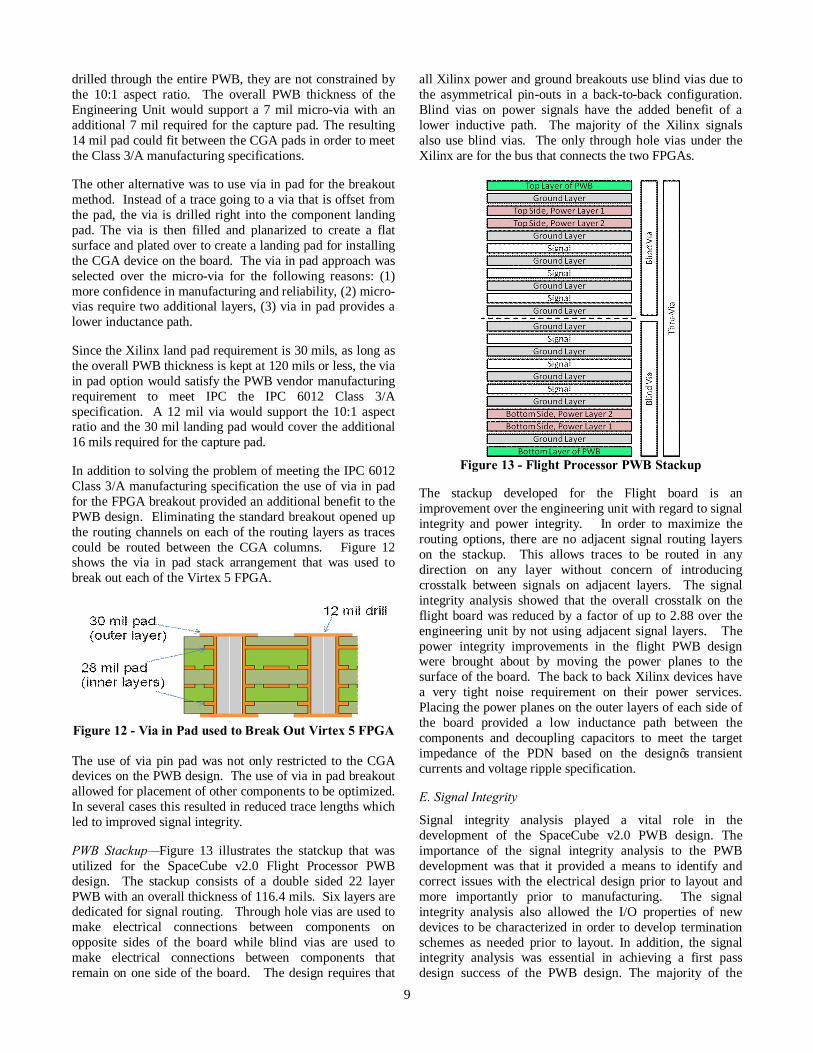
PWB Stackup—Figure 13 illustrates the statckup that was utilized for the SpaceCube v2.0 Flight Processor PWB design. The stackup consists of a double sided 22 layer PWB with an overall thickness of 116.4 mils. Six layers are dedicated for signal routing. Through hole vias are used to make electrical connections between components on opposite sides of the board while blind vias are used to make electrical connections between components that remain on one side of the board. The design requires that
all Xilinx power and ground breakouts use blind vias due to the asymmetrical pin-outs in a back-to-back configuration. Blind vias on power signals have the added benefit of a lower inductive path. The majority of the Xilinx signals also use blind vias. The only through hole vias under the Xilinx are for the bus that connects the two FPGAs.
Figure 13 - Flight Processor PWB Stackup
The stackup developed for the Flight board is an improvement over the engineering unit with regard to signal integrity and power integrity. In order to maximize the routing options, there are no adjacent signal routing layers on the stackup. This allows traces to be routed in any direction on any layer without concern of introducing crosstalk between signals on adjacent layers. The signal integrity analysis showed that the overall crosstalk on the flight board was reduced by a factor of up to 2.88 over the engineering unit by not using adjacent signal layers. The power integrity improvements in the flight PWB design were brought about by moving the power planes to the surface of the board. The back to back Xilinx devices have a very tight noise requirement on their power services. Placing the power planes on the outer layers of each side of the board provided a low inductance path between the components and decoupling capacitors to meet the target impedance of the PDN based on the design’s transient currents and voltage ripple specification.
E. Signal Integrity
Signal integrity analysis played a vital role in the development of the SpaceCube v2.0 PWB design. The importance of the signal integrity analysis to the PWB development was that it provided a means to identify and correct issues with the electrical design prior to layout and more importantly prior to manufacturing. The signal integrity analysis also allowed the I/O properties of new devices to be characterized in order to develop termination schemes as needed prior to layout. In addition, the signal integrity analysis was essential in achieving a first pass design success of the PWB design. The majority of the
10
electrical connections on the SpaceCube v2.0 PWB design are between three FPGA devices and peripheral devices. The FPGAs are packaged as CGA devices. Since the I/O pins of the CGA devices are located under the device, and two of the FPGAs are back to back, it would not be possible to rework the PWB design to address signal integrity issues after manufacturing. A board respin would be required to resolve design issues. The SI analysis was used to analyze all of the electrical interfaces of the PWB design. The analysis identified issues that drove numerous changes to the electrical design, layout and routing of the PWB design prior to manufacturing. The signal integrity analysis was broken down into two phases: pre-route and post route analysis. Each of the phases of the signal integrity and their impact on the design are discussed below.
Pre-route Analysis—The importance of the pre-route analysis is that it provided the ability to obtain preliminary signal integrity analysis of the PWB design and circuit interfaces before layout and routing activities took place. This was a vital step to the PWB design as it provides a means to identify signal integrity issues and to formulate termination schemes to mitigate potential problems. One of the impacts of the pre-route analysis of the development of the SpaceCube v2.0 PWB design is that it significantly reduced the time spent during the layout and routing phases of the PWB design. Since all of the interfaces were simulated during the pre-route analysis, all of the component placement and signal integrity issues were identified and mitigated upfront. This eliminated the need to wait until the post-route analysis to identify issues when making changes to the layout and routing would present significant problems.
An example of where the pre-route analysis had a direct impact on the PWB design was with regard to the DDR SDRAM interfaces. The SpaceCube v2.0 design incorporates four DDR SDRAM that utilize the Stub Series Terminated Logic (SSTL). The recommended termination scheme for bidirectional SSTL logic consists of 4 resistors along with and additional voltage plane, Vt. This termination scheme is designed to reduce reflections on a bus, which will provide faster rise and fall times and reduce the signal settling time resulting in higher possible clock rates.
Implementing this termination scheme on the design would have required a total of 288 resistors for all of the bidirectional SSTL signals of the SDRAM interfaces. Voltages planes would also need to be added to implement Vt. Due to the density of components on the design, there was not enough real estate on the board to accommodate all of these resistors and the voltage planes to implement the full termination scheme. The pre-route analysis was used to develop a layout topology that allowed the termination scheme to be optimized reducing the total number of resistors required to 72. The analysis also showed that Vt was not required in order to support the targeted clock rates of the design. On another interface, the pre-route analysis
was used to show that 100 series termination resistors could be eliminated from the design further reducing component count to optimize board real estate. The pre-route analysis was also essential in identifying sources of overshoot and undershoot that violated the manufacture specification and developing termination strategies to mitigate them prior to the layout and routing.
Another function of the pre-route analysis was to validate the PWB stackup and routing parameters that are supplied by the PWB vendors. The stackup parameters that were obtained by the PWB vendor were entered into the analysis tools in order to verify the overall PWB thickness and that that supplied trace widths achieve the targeted single ended and differential impedance. Since the overall PWB thickness influenced the aspect ratio that drove the allowable via sizes, it was important to verify the accuracy of the parameters supplied by the vendor. It is not uncommon for vendors to overlook copper weight requirements that could lead to incorrect overall PWB thickness calculations. Since the size of the via and capture pads are influence by the overall PWB thickness, independent verification of the calculated PWB thickness is warranted.
Post-route Analysis—Once the entire PWB design was routed the bulk of the signal integrity analysis took place during the post-route analysis. In order to achieve a high fidelity signal integrity analysis the goal was to simulate the board as it was going to be manufactured. During the start of the post-route analysis, manufacturing checks were made to ensure that all of the single ended and differential trace widths were routed per PWB vendor supplied trace widths to ensure that the target impedances were achieved. This was essential since the termination schemes developed during the pre-route analysis were based on targeted trace impedances. Additionally, verifying that the traces are routed at the vendor supplied trace width is important as it has a direct impact on the fidelity crosstalk analysis. This ensures that analysis takes into account the trace widths and separations that reflect what is to be manufactured.
Once all of the manufacturing checks were performed the post-route analysis was used to confirm the termination schemes developed during the pre-route analysis, which was based on estimated trace lengths. This was followed by monotonicity checks and an overshoot/undershoot analysis. Monotonicity checks ensured that critical signals did not glitch in the transition region that could lead to double clocking or unwanted reads/writes. The overshoot/undershoot analysis was used to ensure that all signals switched within the specifications and were below the component manufactures absolute maximum voltage ratings.
The post-route analysis also included a crosstalk analysis. Given the high edge rates and density of nets on a given signal layer of the SpaceCube PWB design, the crosstalk analysis was essential to ensure that unwanted noise would not couple between routed traces. Since it is not possible to
11
resolve crosstalk issues after fabrication, the crosstalk analysis was key to PWB design success. The crosstalk analysis was used to uncover multiple sources of crosstalk in the design that resulted in traces being rerouted to mitigate the violations. Attention was placed on the routing of critical nets such as clocks and differential nets that resulted in crosstalk magnitudes of 10 mV or less. The largest crosstalk magnitude on a non-critical net on the entire PWB design was 70 mV, well within the noise margins for the logic families used in the design.
The post-route signal integrity analysis was also used to extract board timing delays to support a worst cast timing analysis.
The impact of the signal integrity analysis was that it resulted in an accelerated testing and delivery schedule of the SpaceCube v2.0 Processor Card. Signal integrity issues were not encountered during the board level testing phase as all of the issues had been identified and correct prior to manufacturing.
F. Power Integrity
The design of the power distribution network (PDN) of the SpaceCube v2.0 PWB was a significant challenge due to the number of electrical components on the PWB and the number of voltage rails that were required to power each of the components. The purpose of the PDN is to keep the voltage across the component chip constant within a narrow tolerance, minimize ground bounce by providing a low impedance return path for signals, and to minimize EMI problems. If the PDN is not designed correctly excess noise can be present on the voltage rails of the components that can lead to issues such as timing problems or bit failures.
There are 10 distinct voltage planes on the SpaceCube v2.0 PWB design. As such, a power integrity analysis was needed in order to ensure that the PDN design would meet the electrical requirements on each of the voltage planes from DC to high frequency. The power integrity analysis was critical to the design process as it provided a means to identify and correct power distribution problems prior to manufacturing. The power integrity analysis was broken down into two phases: the DC and the AC analysis. Each of the phases of the power integrity and their impact on the design are discussed below.
DC Analysis—The purpose of the DC analysis was to identify excess DC drop and areas of high current density on the PWB design. Since it is was not practical for each of the supply voltages to have their own dedicated plane, power layers in the stackup were shared by multiple supply voltages. This resulted in split planes and distinct power islands. The DC drop analysis ensured that the PDN design had adequate copper and vias to handle the maximum DC current draw with margin on the IR drop.
An example of how the DC drop analysis was used to identify and correct a power distribution problem was with
regard to the 1.0V power plane that is used to power the array logic of the Xilinx FPGAs. This supply voltage has an allowable DC drop of 5% or 50 mV. The DC drop analysis of the 1.0V power plane revealed that the DC drop was 67mV which exceed the requirement. In order to remedy the DC drop issue the overall area of the plane was increased to provide additional copper to meet the DC drop requirement. The strength of the power integrity analysis was that it provided a means to know just how much copper was needed without having to over design the size of the plane. The change to the shape of the power plane resulted in a worst case DC drop of 45.1 mV which met the DC drop requirement with design margin.
Each of the voltage planes in the design was analyzed to ensure that they met their DC drop requirements. The results from the DC analysis were used to increase the copper area of voltage planes as needed to successful achieve the required DC plus margin. The DC analysis was also used to locate areas of high current densities in neckdown areas of a voltage plane and to make improvements to the plane geometries in order to unify the current density distributions.
AC Analysis—The purpose of the AC analysis was to determine the PDN’s ability to deliver power in the frequency domain. The analysis goal was to analyze the PDN impedance across all frequencies and take steps to minimize the impedance. A high impedance PDN will result in inadequate switching currents for components as well as voltage ripple which could lead to signal integrity problems such as bit errors or timing violations. In order to keep the voltage drop on the component supply pins less than the specified voltage ripple, the impedance of the PDN needs to be below a maximum allowable value known as the target impedance. When the impedance profile is kept below the target value across the frequencies of interest (0 Hz up to the knee frequency), the worst case voltage rail noise will be less than the ripple specification.
The important guidelines for the PDN design in order to achieve a design’s target impedance is to use power and ground planes on adjacent layers with thin dielectrics as close to the surface of the board and to use short and wide surface traces between decoupling capacitor pads and the vias to the power and ground planes. The capacitor should be placed to have the lowest loop inductance.
For each of the power planes on the SpaceCube v2.0 PWB design, the target impedance and corresponding knee frequency were calculated. It is left up to the reader to determine how to calculate the target impedance and knee frequency for a PDN design. An AC power integrity analysis was then performed to determine if the board decoupling strategy and inter plane capacitance would meet the target impedance from 0 Hz to the knee frequency.
Figure 14 illustrates the impedance versus frequency profile of the Flash interface voltage plane. Based on the transient current and ripple requirement the target impedance was
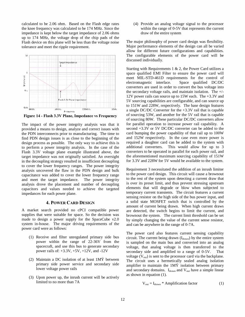
12
calculated to be 2.06 ohm. Based on the Flash edge rates the knee frequency was calculated to be 174 MHz. Since the impedance is kept below the target impedance of 2.06 ohms up to 174 MHz, the voltage drop of the chip pads of the Flash device on this plane will be less than the voltage noise tolerance and meet the ripple requirement.
Figure 14 - Flash 3.3V Plane, Impedance vs Frequency
The impact of the power integrity analysis was that it provided a means to design, analyze and correct issues with the PDN interconnects prior to manufacturing. The time to find PDN design issues is as close to the beginning of the design process as possible. The only way to achieve this is to perform a power integrity analysis. In the case of the Flash 3.3V voltage plane example illustrated above, the target impedance was not originally satisfied. An oversight in the decoupling strategy resulted in insufficient decoupling to cover the lower frequency ranges. The power integrity analysis uncovered the flaw in the PDN design and bulk capacitance was added to cover the lower frequency range and meet the target impedance. The power integrity analysis drove the placement and number of decoupling capacitors and values needed to achieve the targeted impedances for each power plane.
4. POWER CARD DESIGN A market search provided no cPCI compatible power supplies that were suitable for space. So the decision was made to design a power supply for the SpaceCube v2.0 system in-house. The major driving requirements of the power card were as follows:
(1) Receive and filter unregulated primary side bus power within the range of 22-36V from the spacecraft, and use this bus to generate secondary power rails of: +3.3V, +5V, +12V, and -12V
(2) Maintain a DC isolation of at least 1MΩ between primary side power service and secondary side lower voltage power rails
(3) Upon power up, the inrush current will be actively limited to no more than 7A
(4) Provide an analog voltage signal to the processor within the range of 0-5V that represents the current draw of the entire system
The major philosophy of power card design was flexibility. Major performance elements of the design can all be varied allow for different future configurations and capabilities. The configurable elements of the power card will be discussed individually.
Starting with Requirements 1 & 2, the Power Card utilizes a space qualified EMI Filter to ensure the power card will meet MIL-STD-461D requirements for the control of electromagnetic interface. Space qualified DC/DC converters are used in order to convert the bus voltage into the secondary voltage rails, and maintain isolation. The +/-12V power rails can source up to 15W each. The +3.3V and 5V sourcing capabilities are configurable, and can source up to 151W and 228W, respectively. The base design features a single DC/DC Converter for the +3.3V rail that is capable of sourcing 53W, and another for the 5V rail that is capable of sourcing 80W. These particular DC/DC converters allow for parallel operation to increase power rail capability. A second +3.3V or 5V DC/DC converter can be added to the card bumping the power capability of that rail up to 100W and 152W respectively. In the case even more power is required a daughter card can be added to the system with additional converters. This would allow for up to 3 converters to be operated in parallel for each power rail, and the aforementioned maximum sourcing capability of 151W for 3.3V and 228W for 5V would be available to the system.
Requirement 3 necessitated the addition of an inrush limiter to the power card design. This circuit will cause a brownout to the rest of the system upon detecting a current draw that is over its preset limit, and thus prevent stressing upstream elements that will degrade or blow when subjected to temporary current transients. The circuit features a current sensing resistor on the high side of the bus power input, and a solid state MOSFET switch that is controlled by the amount of current being drawn. When high current draws are detected, the switch begins to limit the current, and brownout the system. The current limit threshold can be set by simply changing the value of the current sense resistor, and can be anywhere in the range of 0-7A.
The power card also features current sensing capability circuit. The current being drawn (Idrawn) by the entire system is sampled on the main bus and converted into an analog voltage, that analog voltage is then transferred to the secondary side and amplified to a range of 0-5V. That voltage (Vout) is sent to the processor card via the backplane. The circuit uses a hermetically sealed analog isolation amplifier to maintain the 1MΩ isolation between primary and secondary domains. Idrawn and Vout have a simple linear as shown in equation (1).
Vout = Idrawn * Amplification factor (1)
13
With the change of a few resistors the amplification factor can be changed to allow any current envelope within 0-7A can be converted to the 0-5V analog signal the processor requires. This allows for systems with both low and high power consumptions have a high fidelity signal, and take advantage of the full 0-5V processor input range.
The Power Card handles power sequencing of the secondary voltages to satisfy the requirements of the processor card, in particular the Xilinx FPGA. The Power Card is also responsible for generating a global system reset signal and power loss warning signal. The power loss warning signal is used by the processor card(s) to enter a safe operating mode before power is removed.
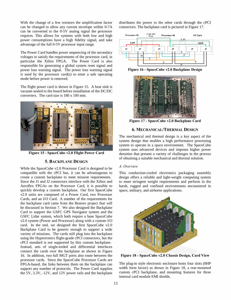
The flight power card is shown in Figure 15. A heat sink is vacuum sealed to the board before installation of the DC/DC converters. The card size is 180 x 100 mm.
Figure 15 - SpaceCube v2.0 Flight Power Card
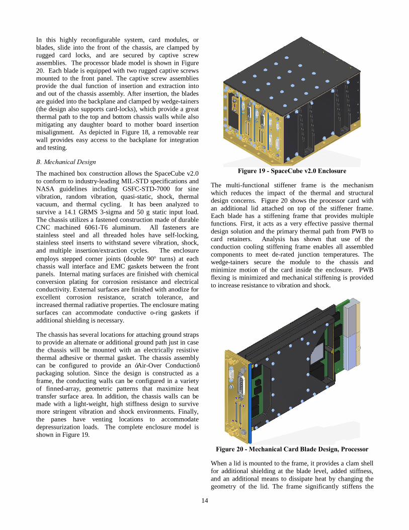
5. BACKPLANE DESIGN While the SpaceCube v2.0 Processor Card is designed to be compatible with the cPCI bus, it can be advantageous to create a custom backplane to meet mission requirements. Since the J1 and J2 connectors interface with the Xilinx and Aeroflex FPGAs on the Processor Card, it is possible to quickly develop a custom backplane. Our first SpaceCube v2.0 units are composed of a Power Card, two Processor Cards, and an I/O Card. A number of the requirements for the backplane card came from the Restore project that will be discussed in Section 7. We also designed the Backplane Card to support the GSFC GPS Navigator system and the GSFC Lidar system, which both require a base SpaceCube v2.0 system (Power and Processor) along with a custom I/O card. In the end, we designed the first SpaceCube v2.0 Backplane Card to be generic enough to support a wide variety of missions. The cards still plug into the backplane using the Hypertronics flight-grade cPCI connectors, but the cPCI standard is not supported by this custom backplane. Instead, sets of single-ended and differential interfaces connect the cards over the backplane as shown in Figure 16. In addition, two full MGT ports also route between the processor cards. Since the SpaceCube Processor Cards are FPGA-based, the links between them on the backplane can support any number of protocols. The Power Card supplies the 5V, 3.3V, -12V, and 12V power rails and the backplane
distributes the power to the other cards through the cPCI connectors. The backplane card is pictured in Figure 17.
Figure 16 - SpaceCube v2.0 Backplane Design
Figure 17 - SpaceCube v2.0 Backplane Card
6. MECHANICAL/THERMAL DESIGN The mechanical and thermal design is a key aspect of the system design that enables a high performance processing system to operate in a space environment. The SpaceCube system uses advanced devices and imposes higher power densities that present a variety of challenges in the process of obtaining a suitable mechanical and thermal solution.
A. Overview
This conduction-cooled electronics packaging assembly design offers a reliable and light-weight computing system to meet stringent weight requirements and perform in the harsh, rugged and confined environments encountered in space, military, and airborne applications.
Figure 18 - SpaceCube v2.0 Chassis Design, Card View
The plug-in style electronic enclosure hosts four slots (8HP width form factor) as shown in Figure 18, a rear-mounted custom cPCI backplane, and mounting features for three internal card module EMI shields.
14
In this highly reconfigurable system, card modules, or blades, slide into the front of the chassis, are clamped by rugged card locks, and are secured by captive screw assemblies. The processor blade model is shown in Figure 20. Each blade is equipped with two rugged captive screws mounted to the front panel. The captive screw assemblies provide the dual function of insertion and extraction into and out of the chassis assembly. After insertion, the blades are guided into the backplane and clamped by wedge-tainers (the design also supports card-locks), which provide a great thermal path to the top and bottom chassis walls while also mitigating any daughter board to mother board insertion misalignment. As depicted in Figure 18, a removable rear wall provides easy access to the backplane for integration and testing.
B. Mechanical Design
The machined box construction allows the SpaceCube v2.0 to conform to industry-leading MIL-STD specifications and NASA guidelines including GSFC-STD-7000 for sine vibration, random vibration, quasi-static, shock, thermal vacuum, and thermal cycling. It has been analyzed to survive a 14.1 GRMS 3-sigma and 50 g static input load. The chassis utilizes a fastened construction made of durable CNC machined 6061-T6 aluminum. All fasteners are stainless steel and all threaded holes have self-locking, stainless steel inserts to withstand severe vibration, shock, and multiple insertion/extraction cycles. The enclosure employs stepped corner joints (double 90° turns) at each chassis wall interface and EMC gaskets between the front panels. Internal mating surfaces are finished with chemical conversion plating for corrosion resistance and electrical conductivity. External surfaces are finished with anodize for excellent corrosion resistance, scratch tolerance, and increased thermal radiative properties. The enclosure mating surfaces can accommodate conductive o-ring gaskets if additional shielding is necessary.
The chassis has several locations for attaching ground straps to provide an alternate or additional ground path just in case the chassis will be mounted with an electrically resistive thermal adhesive or thermal gasket. The chassis assembly can be configured to provide an ‘Air-Over Conduction’ packaging solution. Since the design is constructed as a frame, the conducting walls can be configured in a variety of finned-array, geometric patterns that maximize heat transfer surface area. In addition, the chassis walls can be made with a light-weight, high stiffness design to survive more stringent vibration and shock environments. Finally, the panes have venting locations to accommodate depressurization loads. The complete enclosure model is shown in Figure 19.
Figure 19 - SpaceCube v2.0 Enclosure
The multi-functional stiffener frame is the mechanism which reduces the impact of the thermal and structural design concerns. Figure 20 shows the processor card with an additional lid attached on top of the stiffener frame. Each blade has a stiffening frame that provides multiple functions. First, it acts as a very effective passive thermal design solution and the primary thermal path from PWB to card retainers. Analysis has shown that use of the conduction cooling stiffening frame enables all assembled components to meet de-rated junction temperatures. The wedge-tainers secure the module to the chassis and minimize motion of the card inside the enclosure. PWB flexing is minimized and mechanical stiffening is provided to increase resistance to vibration and shock.
Figure 20 - Mechanical Card Blade Design, Processor
When a lid is mounted to the frame, it provides a clam shell for additional shielding at the blade level, added stiffness, and an additional means to dissipate heat by changing the geometry of the lid. The frame significantly stiffens the
15
electronic card assembly reducing potential for board flexing induced solder joint fatigue. When added stiffness and shielding on both sides of the blade are necessary, frames and shields are mounted back-to-back on the PWB.
The frame has the design features to integrate a heat pipe assembly or heat strap, thus providing a direct thermal path from the Xilinx FPGAs to the base card retainers. By reducing temperature differences, physical strain resulting from differing thermal expansion coefficients of components and board materials is minimized. This results in improved reliability and allows components to survive longer duration, wider temperature extreme missions with use of completely passive design solutions meeting the -40C to 65C temperature range relying on temperature control only at the base.
C. Thermal Analysis
The base-plate, conduction-cooled packaging design is capable of operating from -40°C to 65°C.
Several thermal, structural, and thermo-mechanical analyses trade studies were conducted to achieve an optimal balance of designing for processing performance, PWB layout IPC Class 3/A requirements, assembly of components on the dense PWB, and environmental performance goals. The thermal trade study compared the use of highly conductive materials (composites, aluminum impregnated graphite, and aluminum 6061) at the chassis, blade assembly, and/or component level. It also compared the addition of design options such as chassis wall thickness, PWB copper density, component layout, and PWB blade orientation in the chassis. The results demonstrated that focus on component level thermal design solutions and component placement was needed to most efficiently meet thermal requirements. EEE components meet de-rated junction temperature limits with the baseline, aluminum chassis design without heat pipes or heat straps. The box thermal model is shown in Figure 21. The processor card and power card thermal models are shown in Figure 22.
Figure 21 - SpaceCube v2.0 Box-Level Thermal Profile
Figure 22 - Processor and Power Card Thermal Profiles
D. Structural Analysis
A structural finite element analysis was conducted to assess the reliability of component leads and solder joints, PWBs, chassis components, and structural hardware. The random vibration input was produced conservatively by using the 3 sigma Mile’s Equation acceleration and assuming a conservative damping ratio of 2%. The quasi-static analysis uses the conservative no-test factors of safety from GSFC-STD-7000. The model includes localized masses of components and heat pipe assemblies without adding the local stiffness they contribute. Standard validity checks were performed to ensure the results are reasonable. The results provide a demonstration by analysis that the electrical component solder joints should survive an almost infinite number of stress reversals prior to PWB deflection induced fatigue.
Figure 23 - SpaceCube v2.0 Structural Analysis
E. Test Plan
SpaceCube v2.0 will undergo two qualification test campaigns. First, a Xilinx Virtex-5 CGA test will qualify the innovative and unique PWB design, CGA back-to-back implementation, and overall packaging design. Daisy-chain V5 CGA components will be assembled onto a flight like PWB and tested in several thermo-mechanical card module configurations. Vibration testing will be conducted per GSFC-STD-7000 with 14.1 GRMS input (2min/axis) and a quasi-static strength test in a hard mounted full chassis assembly. Thermal cycling will be performed per IPC-9701. PWBs will undergo interconnect stress testing (IST). 2D x-
16
ray and 40X magnified optical inspection will be conducted at various stages of the test, and destructive physical analysis (DPA) of the CGA and PWB will be conducted after the test is completed.
Second, the SpaceCube v2.0 system will also undergo qualification testing with functional testing performed at various stages throughout the test. This test will include thermal vacuum (12 cycles, -40 to +65C) and vibration testing (14.1 GRMS, 2 min per axis) per GSFC-STD-7000.
7. MISSION CASE STUDY A. ISS SpaceCube v2.0 Experiment
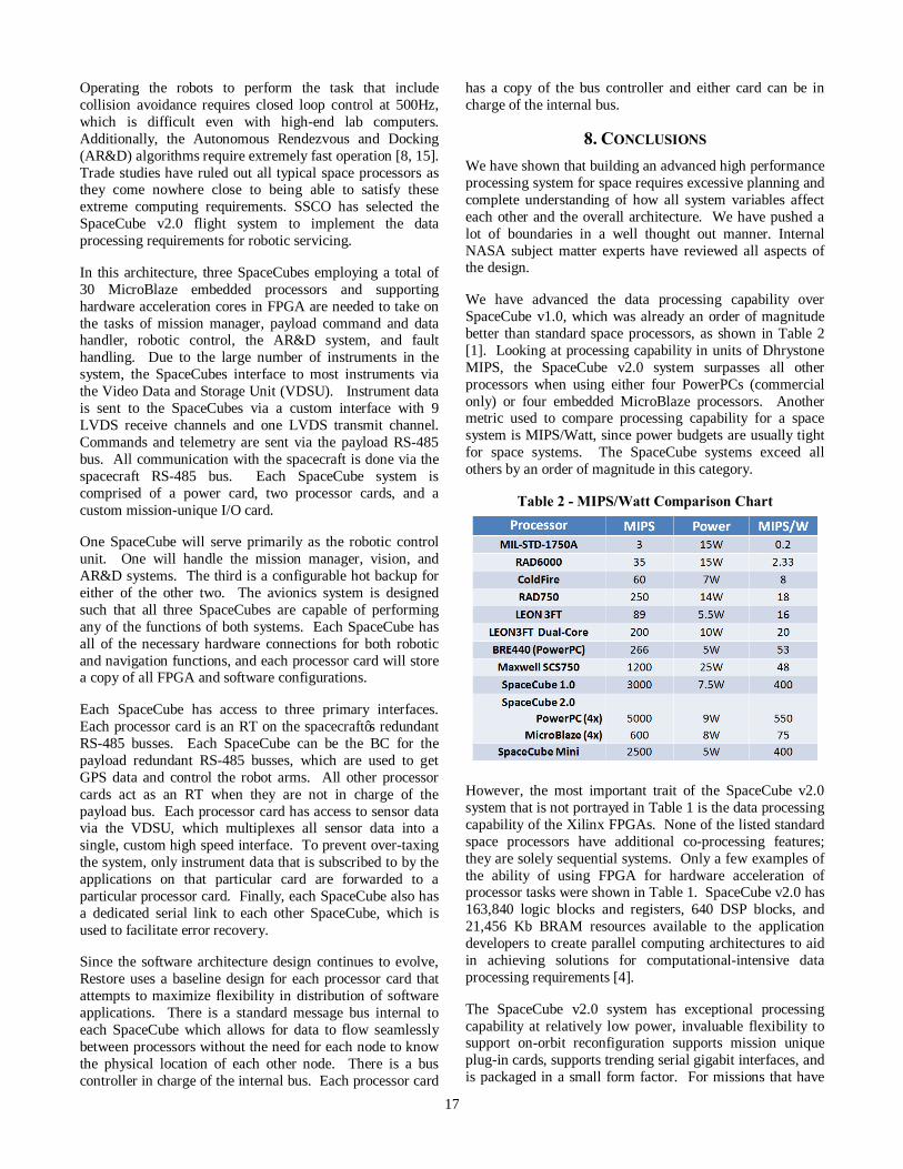
The ISE 2.0 experiment, which is a follow-on to our SpaceCube v1.0 payload on MISSE-7 [1, 5, 10, 17], is installed on the DoD Space Test Program Houston 4 (STP-H4) payload that was activated on the ISS in August 2013. The ISE 2.0 consists of a Power Unit, SpaceCube v2.0 Engineering Model, a suite of high definition cameras, and a Goddard instrument called FireStation. The SpaceCube v2.0 EM is used to control the cameras and FireStation instrument. The communication link between ISE 2.0 and the ISS goes through the main avionics of STP-H4, which is a SpaceCube v1.0 system [1, 7, 11]. Figure 25 shows the STP-H4 payload. All red boxes are Goddard deliveries.
All three Xilinx FPGAs are used on this experiment, although only a small percentage of FPGA resources are used. Each FPGA uses one embedded PowerPC440 for
processing requirements. One FPGA is used to control the camera instrument. A second FPGA is used to control the FireStation instrument. The third FPGA is the main controller which handles the STP-H4 interface, enabling instrument loads, gathering telemetry from the two other Xilinx FPGAs. The main controller FPGA also handles configuration scrubbing of all three FPGAs. This FPGA collects radiation SEU statistics that are included in telemetry. The system supports on-orbit reconfiguration.
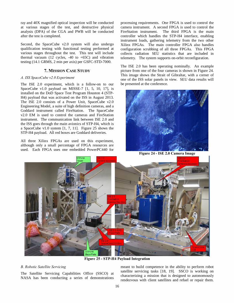
The ISE 2.0 has been operating nominally. An example picture from one of the four cameras is shown in Figure 24. This image shows the Strait of Gibraltar, with a corner of one of the ISS solar panels in view. SEU data results will be presented at the conference.
Figure 24 - ISE 2.0 Camera Image
Figure 25 - STP-H4 Payload Integration
B. Robotic Satellite Servicing
The Satellite Servicing Capabilities Office (SSCO) at NASA has been conducting a series of demonstrations
meant to build competence in the ability to perform robot satellite servicing tasks [18, 19]. SSCO is working on characterizing a mission that is designed to autonomously rendezvous with client satellites and refuel or repair them.
17
Operating the robots to perform the task that include collision avoidance requires closed loop control at 500Hz, which is difficult even with high-end lab computers. Additionally, the Autonomous Rendezvous and Docking (AR&D) algorithms require extremely fast operation [8, 15]. Trade studies have ruled out all typical space processors as they come nowhere close to being able to satisfy these extreme computing requirements. SSCO has selected the SpaceCube v2.0 flight system to implement the data processing requirements for robotic servicing.
In this architecture, three SpaceCubes employing a total of 30 MicroBlaze embedded processors and supporting hardware acceleration cores in FPGA are needed to take on the tasks of mission manager, payload command and data handler, robotic control, the AR&D system, and fault handling. Due to the large number of instruments in the system, the SpaceCubes interface to most instruments via the Video Data and Storage Unit (VDSU). Instrument data is sent to the SpaceCubes via a custom interface with 9 LVDS receive channels and one LVDS transmit channel. Commands and telemetry are sent via the payload RS-485 bus. All communication with the spacecraft is done via the spacecraft RS-485 bus. Each SpaceCube system is comprised of a power card, two processor cards, and a custom mission-unique I/O card.
One SpaceCube will serve primarily as the robotic control unit. One will handle the mission manager, vision, and AR&D systems. The third is a configurable hot backup for either of the other two. The avionics system is designed such that all three SpaceCubes are capable of performing any of the functions of both systems. Each SpaceCube has all of the necessary hardware connections for both robotic and navigation functions, and each processor card will store a copy of all FPGA and software configurations.
Each SpaceCube has access to three primary interfaces. Each processor card is an RT on the spacecraft’s redundant RS-485 busses. Each SpaceCube can be the BC for the payload redundant RS-485 busses, which are used to get GPS data and control the robot arms. All other processor cards act as an RT when they are not in charge of the payload bus. Each processor card has access to sensor data via the VDSU, which multiplexes all sensor data into a single, custom high speed interface. To prevent over-taxing the system, only instrument data that is subscribed to by the applications on that particular card are forwarded to a particular processor card. Finally, each SpaceCube also has a dedicated serial link to each other SpaceCube, which is used to facilitate error recovery.
Since the software architecture design continues to evolve, Restore uses a baseline design for each processor card that attempts to maximize flexibility in distribution of software applications. There is a standard message bus internal to each SpaceCube which allows for data to flow seamlessly between processors without the need for each node to know the physical location of each other node. There is a bus controller in charge of the internal bus. Each processor card
has a copy of the bus controller and either card can be in charge of the internal bus.
8. CONCLUSIONS We have shown that building an advanced high performance processing system for space requires excessive planning and complete understanding of how all system variables affect each other and the overall architecture. We have pushed a lot of boundaries in a well thought out manner. Internal NASA subject matter experts have reviewed all aspects of the design.
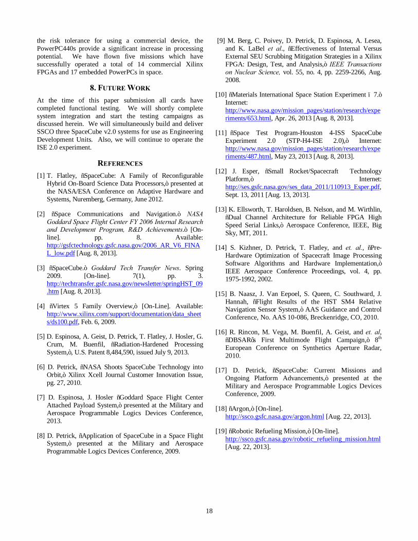
We have advanced the data processing capability over SpaceCube v1.0, which was already an order of magnitude better than standard space processors, as shown in Table 2 [1]. Looking at processing capability in units of Dhrystone MIPS, the SpaceCube v2.0 system surpasses all other processors when using either four PowerPCs (commercial only) or four embedded MicroBlaze processors. Another metric used to compare processing capability for a space system is MIPS/Watt, since power budgets are usually tight for space systems. The SpaceCube systems exceed all others by an order of magnitude in this category.
Table 2 - MIPS/Watt Comparison Chart
However, the most important trait of the SpaceCube v2.0 system that is not portrayed in Table 1 is the data processing capability of the Xilinx FPGAs. None of the listed standard space processors have additional co-processing features; they are solely sequential systems. Only a few examples of the ability of using FPGA for hardware acceleration of processor tasks were shown in Table 1. SpaceCube v2.0 has 163,840 logic blocks and registers, 640 DSP blocks, and 21,456 Kb BRAM resources available to the application developers to create parallel computing architectures to aid in achieving solutions for computational-intensive data processing requirements [4].
The SpaceCube v2.0 system has exceptional processing capability at relatively low power, invaluable flexibility to support on-orbit reconfiguration supports mission unique plug-in cards, supports trending serial gigabit interfaces, and is packaged in a small form factor. For missions that have
18
the risk tolerance for using a commercial device, the PowerPC440s provide a significant increase in processing potential. We have flown five missions which have successfully operated a total of 14 commercial Xilinx FPGAs and 17 embedded PowerPCs in space.
8. FUTURE WORK At the time of this paper submission all cards have completed functional testing. We will shortly complete system integration and start the testing campaigns as discussed herein. We will simultaneously build and deliver SSCO three SpaceCube v2.0 systems for use as Engineering Development Units. Also, we will continue to operate the ISE 2.0 experiment.
REFERENCES [1] T. Flatley, “SpaceCube: A Family of Reconfigurable
Hybrid On-Board Science Data Processors,” presented at the NASA/ESA Conference on Adaptive Hardware and Systems, Nuremberg, Germany, June 2012.
[2] “Space Communications and Navigation.” NASA Goddard Space Flight Center FY 2006 Internal Research and Development Program, R&D Achievements.” [On-line]. pp. 8. Available: http://gsfctechnology.gsfc.nasa.gov/2006_AR_V6_FINAL_low.pdf [Aug. 8, 2013].
[3] “SpaceCube.” Goddard Tech Transfer News. Spring 2009. [On-line]. 7(1), pp. 3. http://techtransfer.gsfc.nasa.gov/newsletter/springHST_09.htm [Aug. 8, 2013].
[4] “Virtex 5 Family Overview,” [On-Line]. Available: http://www.xilinx.com/support/documentation/data_sheets/ds100.pdf, Feb. 6, 2009.
[5] D. Espinosa, A. Geist, D. Petrick, T. Flatley, J. Hosler, G. Crum, M. Buenfil, “Radiation-Hardened Processing System,”, U.S. Patent 8,484,590, issued July 9, 2013.
[6] D. Petrick, “NASA Shoots SpaceCube Technology into Orbit,” Xilinx Xcell Journal Customer Innovation Issue, pg. 27, 2010.
[7] D. Espinosa, J. Hosler “Goddard Space Flight Center Attached Payload System,” presented at the Military and Aerospace Programmable Logics Devices Conference, 2013.
[8] D. Petrick, “Application of SpaceCube in a Space Flight System,” presented at the Military and Aerospace Programmable Logics Devices Conference, 2009.
[9] M. Berg, C. Poivey, D. Petrick, D. Espinosa, A. Lesea, and K. LaBel et al., “Effectiveness of Internal Versus External SEU Scrubbing Mitigation Strategies in a Xilinx FPGA: Design, Test, and Analysis,” IEEE Transactions on Nuclear Science, vol. 55, no. 4, pp. 2259-2266, Aug. 2008.
[10] “Materials International Space Station Experiment – 7.” Internet: http://www.nasa.gov/mission_pages/station/research/experiments/653.html, Apr. 26, 2013 [Aug. 8, 2013].
[11] “Space Test Program-Houston 4-ISS SpaceCube Experiment 2.0 (STP-H4-ISE 2.0),” Internet: http://www.nasa.gov/mission_pages/station/research/experiments/487.html, May 23, 2013 [Aug. 8, 2013].
[12] J. Esper, “Small Rocket/Spacecraft Technology Platform,” Internet: http://ses.gsfc.nasa.gov/ses_data_2011/110913_Esper.pdf, Sept. 13, 2011 [Aug. 13, 2013].
[13] K. Ellsworth, T. Haroldsen, B. Nelson, and M. Wirthlin, “Dual Channel Architecture for Reliable FPGA High Speed Serial Links,” Aerospace Conference, IEEE, Big Sky, MT, 2011.
[14] S. Kizhner, D. Petrick, T. Flatley, and et. al., “Pre-Hardware Optimization of Spacecraft Image Processing Software Algorithms and Hardware Implementation,” IEEE Aerospace Conference Proceedings, vol. 4, pp. 1975-1992, 2002.
[15] B. Naasz, J. Van Eepoel, S. Queen, C. Southward, J. Hannah, “Flight Results of the HST SM4 Relative Navigation Sensor System,” AAS Guidance and Control Conference, No. AAS 10-086, Breckenridge, CO, 2010.
[16] R. Rincon, M. Vega, M. Buenfil, A. Geist, and et. al, “DBSAR’s First Multimode Flight Campaign,” 8th European Conference on Synthetics Aperture Radar, 2010.
[17] D. Petrick, “SpaceCube: Current Missions and Ongoing Platform Advancements,” presented at the Military and Aerospace Programmable Logics Devices Conference, 2009.
[18] “Argon,” [On-line]. http://ssco.gsfc.nasa.gov/argon.html [Aug. 22, 2013].
[19] “Robotic Refueling Mission,” [On-line]. http://ssco.gsfc.nasa.gov/robotic_refueling_mission.html [Aug. 22, 2013].
19
BIOGRAPHY David Petrick started his career at NASA in 2000. He has a wide range of experience building Xilinx FPGA-based systems for space flight including FPGA design, radiation mitigation testing, PCB design, reconfigurable system design, and mission operations. He was the lead design engineer on the
SpaceCube v1.0 and v2.0 processor cards including embedded systems framework, FPGA core development, and electrical design, responsible engineer for the RNS SpaceCube system build, delivery, and shuttle payload operations, lead engineer for the MISSE-7 and ISE2.0 SpaceCube hardware deliveries, and systems lead on the SpaceCube v2.0 development effort. He is currently the Embedded Processing group leader within the Science Data Processing Branch and SpaceCube Program Technical Development Lead. He has a BSEE from the University of Pittsburgh and a MSEE from the Johns Hopkins University.
Alessandro Geist received his B.S. in Computer Engineering from Johns Hopkins University and his M.S. in Electrical Engineering from the University of Maryland, College Park. He has worked at NASA GSFC in the Science Data Processing Branch since 2006. He has had significant experience
implementing and accelerating on-board processing algorithms in FPGAs on a variety of missions including DBSAR, URAD, GNFIR/RNS, MISSE-7, and other internal research and development efforts. He has also been extensively involved in flight processor card design including being the lead design engineer of the SpaceCube 1.5 and co-lead design engineer of the SpaceCube Mini processor systems. In addition, he was the FPGA development lead on ISE 2.0 and the avionics lead engineer on the SMART sounding rocket mission. He is currently developing much of the FPGA infrastructure for the SpaceCube 2.0 processor system, and is also the experiment lead for ISEM on STP-H5. Dennis Albaijes is a senior electrical engineer in the Flight Data Systems and Radiation Effects Branch at NASA’s Goddard Space Flight Center. His expertise is in hardware design and development of high-reliability flight data systems. His experience includes ASIC and FPGA designs on Command and Data Handling (C&DH) subsystem electronics on multiple Small Explorers (SMEX) missions as well as science instrument electronics on the SWIFT and DSCOVR missions. His area of expertise also includes signal integrity and printed wiring board (PWB) design. He served as the
lead PWB design and signal integrity engineer on critical C&DH subsystem electronics developments for the LRO, GPM and MMS missions as well as the SpaceCube v2.0 design. He has received a NASA Exceptional Engineering Medal for process development in signal integrity analysis and PWB design that improved quality and reliability of flight electronic hardware for space flight applications. He has a B.S. in Electrical Engineering from Florida International University and an M.S. in Electrical Engineering from the Johns Hopkins University.
Milton Davis started his career at NASA in 2000. He has experience on several missions serving as an attitude control system contracting officer’s technical representative (COR) and component hardware lead for star tracker systems. In this role he is acting as the technical authority and liaison between
the project and external vendor and is responsible for the requirement development, selection, procurement, oversight, and integration and test activities of the system onto the spacecraft. He also has design, analysis, assembly, and integration and testing, experience as the component and chassis assembly level. He has served as the packaging lead for GPS processor, GPS RF, power, command and data handling, and propulsion deployment electronic systems. He is a co-lead for the NASA-wide Avionics Community of Packaging Sub-committee (CoSP). He is a co-patent recipient for a demise-able reaction wheel assembly. He is currently serving as the electronics packaging lead for SpaceCube v2.0. He has a BS in aerospace and aeronautical engineering from Purdue University and a MS in project/ technical management from the Johns Hopkins University.
Pietro Sparacino started his career at NASA in 2003. His electrical design experience covers a variety of disciplines, including mixed-signal circuit board designs, power design, FPGA design, control loops, and PCB design. He also has experience in verification and validation, parts engineering,
reliability engineering. In the past he served as the lead design engineer for the COTS/CRS C&DH Power Supply Unit, and the ARGON Power Control Unit. He is currently the lead design engineer for the SpaceCube v2.0 Power Card, and the responsible engineer for the LCRD Modem Digital Board. He has a BSEE from the University of Maryland College Park, and is working toward an MSEE from the Johns Hopkins University.
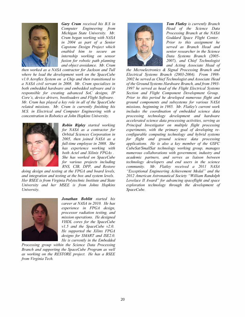
20
Gary Crum received his B.S in Computer Engineering from Michigan State University. Mr. Crum began working with NASA in 2004 as part of a Senior Capstone Design Project which enabled him to secure an internship working on sensor fusion for robotic path planning and object avoidance. Mr. Crum
then worked as a NASA contractor for Jackson and Tull where he lead the development work on the SpaceCube v1.0 Aeroflex System on a Chip and then transitioned to a NASA civil servant in 2008. Mr. Crum specializes in both embedded hardware and embedded software and is responsible for creating advanced SoC designs, IP Core’s, device drivers, bootloaders and Flight Software. Mr. Crum has played a key role in all of the SpaceCube related missions. Mr. Crum is currently finishing his M.S. in Electrical and Computer Engineering with a concentration in Robotics at John Hopkins University.
Robin Ripley started working for NASA as a contractor for Orbital Sciences Corporation in 2005, then joined NASA as a full-time employee in 2008. She has experience working with both Actel and Xilinix FPGAs . She has worked on SpaceCube for various projects including RNS, CIB, DPP, and Restore
doing design and testing at the FPGA and board levels, and integration and testing at the box and system levels. Her BSEE is from Virginia Polytechnic Institute and State University and her MSEE is from Johns Hopkins University.
Jonathan Boblitt started his career at NASA in 2010. He has experience in FPGA design, processor radiation testing, and mission operations. He designed VHDL cores for the SpaceCube v1.5 and the SpaceCube v2.0. He supported the Xilinx FPGA designs for SMART and ISE2.0. He is currently in the Embedded
Processing group within the Science Data Processing Branch and supporting the SpaceCube Program as well as working on the RESTORE project. He has a BSEE from Virginia Tech.
Tom Flatley is currently Branch Head of the Science Data Processing Branch at the NASA Goddard Space Flight Center. Prior to this assignment he served as Branch Head and senior researcher in the Science Data Systems Branch (2005-2007), and Chief Technologist and Acting Associate Head of
the Microelectronics & Signal Processing Branch and Electrical Systems Branch (2003-2004). From 1998-2002 he served as Chief Technologist and Associate Head of the Ground Systems Hardware Branch, and from 1993-1997 he served as head of the Flight Electrical Systems Section and Flight Component Development Group. Prior to this period he developed numerous flight and ground components and subsystems for various NASA missions, beginning in 1985. Mr. Flatley's current work includes the coordination of embedded science data processing technology development and hardware accelerated science data processing activities, serving as Principal Investigator on multiple flight processing experiments, with the primary goal of developing re-configurable computing technology and hybrid systems for flight and ground science data processing applications. He is also a key member of the GSFC CubeSat/SmallSat technology working group, manages numerous collaborations with government, industry and academic partners, and serves as liaison between technology developers and end users in the science community. Mr. Flatley received a 2011 NASA “Exceptional Engineering Achievement Medal” and the 2012 American Astronautical Society “William Randolph Lovelace II Award” for advancing spaceflight and space exploration technology through the development of SpaceCube.