Embed Size (px)
Citation preview
7/30/2019 Space Vector Modulation Control of an AC–DC–AC061
http://slidepdf.com/reader/full/space-vector-modulation-control-of-an-acdcac061 1/9
1470 IEEE TRANSACTIONS ON POWER ELECTRONICS, VOL. 21, NO. 5, SEPTEMBER 2006
Space Vector Modulation Control of an AC–DC–ACConverter With a Front-End Diode Rectifier and
Reduced DC-link CapacitorXiyou Chen and Mehrdad Kazerani , Senior Member, IEEE
Abstract—In this paper, the control of an ac–dc–ac converterwith a front-end diode rectifier and reduced dc-link capacitorbased on the space vector modulation strategy is investigated. Themodulation index is time-varying and determined by the instanta-neous value of the dc voltage measured by a voltage sensor. Usinga small bipolar capacitor, instead of a large electrolytic capacitoron the dc-link, increases the lifetime of the converter and reducesits size. The input current quality of this converter has been shownto be superior to that of the conventional ac–dc–ac converter withfront-end diode rectifier. The perfectly sinusoidal local average
output voltage can still be achieved under unbalanced inputvoltage condition by implementing a time-varying modulationindex. The rule for determining the dc capacitance has also beenstudied in this paper. The simulation results obtained from PSIMsimulation software and experimental results obtained from thelab prototype are used to verify the theoretical expectations.
Index Terms—AC–DC–AC converter, front-end diode rectifier,reduced dc capacitor, space vector modulation, unbalanced inputvoltage.
I. INTRODUCTION
IN RECENT years, the trend in the design of ac–dc–ac con-verters for motor drive applications has been in the direction
of reducing the size, integrating the converter with the motor,
improving the efficiency and lifetime, and reducing the cost. As
a result, eliminating or reducing the size of the dc-link capacitor
has received a lot of attention [1], [2]. Replacing large dc-link
electrolytic capacitors with small nonelectrolytic capacitors of-
fers the advantages of compact size and longer lifetime.
Many researchers have investigated the performance of
ac–dc–ac converters with front-end controlled rectifier and
without dc-link capacitors or ac–ac converters such as indirect
matrix converters in motor drive applications [3], [4]. Nearly
sinusoidal output voltage and input current waveforms, without
low-order harmonics, as well as unity or regulated input powerfactor can be achieved in these converters. Because of the
capability of power regeneration and high quality of waveforms
on both input and output sides, these converters are widely
Manuscript received February 8, 2005; revised July 29, 2005. Recommendedby Associate Editor B. Wu.
X. Chen is with the Department of Electrical and Electronics Engineering,Dalian University of Technology, Dalian 116023, China (e-mail: [email protected]).
M. Kazerani is with the Department of Electrical and Computer Engi-neering, University of Waterloo, Waterloo, ON N2L 3G1, Canada (e-mail:[email protected]).
Digital Object Identifier 10.1109/TPEL.2006.880236
used in medium or high power industrial applications or when
frequent start/stop operations are required.
On the other hand, there are many low-power industrial appli-
cations such as fan and pump drive systems, where it is not fea-
sible to regenerate energy from the load to the source. In these
applications, the front-end diode rectifier ac–dc–ac converters
are still being used because of their lower cost and higher reli-
ability. In the dc–ac stage of such converters, sinusoidal pulse
width modulation (SPWM) or space vector pulse width mod-ulation (SVPWM) are often used in order to obtain sinusoidal
output voltage waveforms. The operation of SPWM inverters
are based on the comparison between the output voltage refer-
ence and a triangular carrier signal to generate the switch con-
trol signals or duty cycles. In these inverters, the dc-link voltage
should be kept constant and a large electrolytic capacitor should
be used in the dc-link. In SVPWM inverters, six fixed active
voltage vectors and two zero vectors are used to synthesize the
rotating desired output voltage vector [5]. The switch duty cy-
cles are calculated according to the position of the desired output
voltage vector with respect to the two adjacent active fixed vec-
tors. In this case, too, a constant dc-link voltage should be main-
tained.In this paper, a novel SVPWM strategy based on time-varying
dc-link voltage is investigated for front-end diode rectifier
ac–dc–ac converter with a small nonelectrolytic dc-link capac-
itor which provides snubbing. The lifetime of the converter can
be increased and its size reduced by adopting this strategy. A
comparative evaluation with respect to the ac–dc–ac converter
with dc-link electrolytic capacitor has been carried out based
on constant motor drive strategy. Simulations using PSIM
software package and experiments on a lab prototype have been
performed to verify the validity of the method proposed in this
paper.
II. FUNDAMENTALS OF SPACE VECTOR MODULATED INVERTER
BASED ON CONSTANT DC-LINK VOLTAGE
The ideal local average values of the output three-phase
line-to-line voltages with amplitude , angular frequency ,
and initial phase angle , can be expressed as
(1)
These voltages can be represented in a three-axis frame, with the
axes , , and phase shifted by 2 3 radians with
0885-8993/$20.00 © 2006 IEEE
7/30/2019 Space Vector Modulation Control of an AC–DC–AC061
http://slidepdf.com/reader/full/space-vector-modulation-control-of-an-acdcac061 2/9
CHEN AND KAZERANI: SPACE VECTOR MODULATION CONTROL 1471
Fig. 1. Three-axis frame, rotating space vector, and three-phase output volt-
ages.
respect to one another, as shown in Fig. 1. The instantaneous
values , , and are equal to the projections of a ro-
tating voltage vector along the axes of , , and , re-
spectively. This rotating vector is called the voltage space vector
and is determined as follows:
(2)
For the three-phase balanced voltages expressed in (1), the
voltage space vector (2) can be simplified as
(3)
where represents the initial position
(at 0) of .
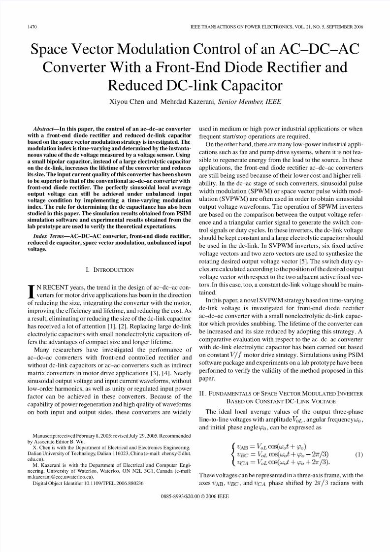
In the dc–ac inverter shown in Fig. 2, there are 8 possible
switch states. Each of these states refers to a certain set of output
voltages ( , and ) and therefore a specific voltage
space vector. The six nonzero active vectors with the same am-
plitude of 2 3 , and the two zero vectors, resulting from
the eight switch states, are shown in Fig. 3 and Table I. For ex-
ample, in the switch state ( ), where the top switch in leg
A and bottom switches in legs B and C of inverter are ON
and
and
(4)
For the switch state ( ), the equivalent circuit of Fig. 4 can
be obtained. From Fig. 4,
(5)
At any moment of time, one can get any of active and zerovectors by selecting the corresponding switch states shown in
Fig. 2. Inverter with constant dc-side voltage.
Fig. 3. Active voltage space vectors.
TABLE ISWITCH STATES, VOLTAGE SPACE VECTORS AND
PHASE-A V OLTAGE( j V j = ( 2 =
p
3 ) V )
Fig. 4. Equivalent circuit for switch state (p ; n ; n
).
Table I. These vectors can be used to synthesize approximately
the rotating output voltage space vector . From the desiredposition of , two adjacent active vectors and , and a
7/30/2019 Space Vector Modulation Control of an AC–DC–AC061
http://slidepdf.com/reader/full/space-vector-modulation-control-of-an-acdcac061 3/9
1472 IEEE TRANSACTIONS ON POWER ELECTRONICS, VOL. 21, NO. 5, SEPTEMBER 2006
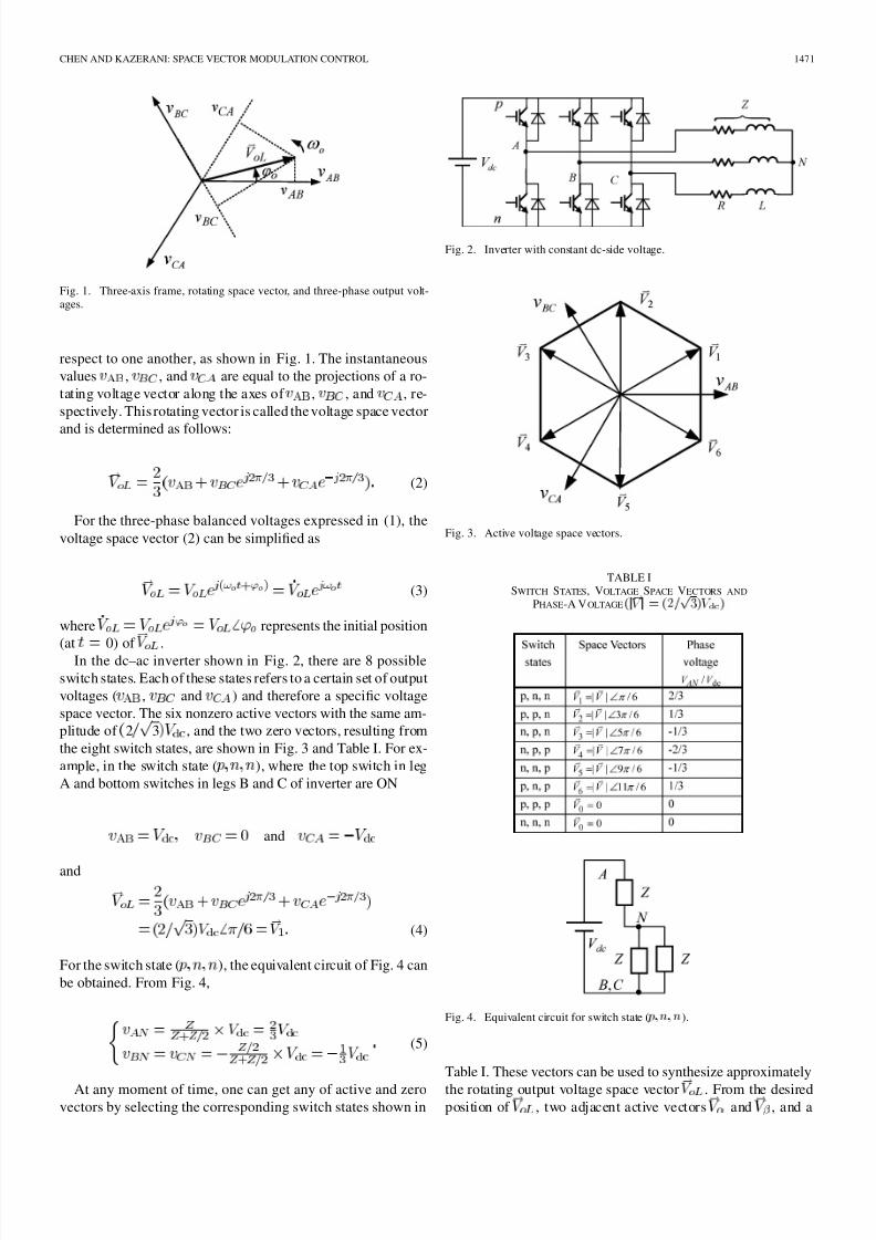
Fig. 5. Synthesis of output voltage space vector.
zero vector are selected to construct , as formulated in (6)
and shown in Fig. 5
(6)
where , and are the duty ratios of the switch states
corresponding to the active vectors , , and , respectively.Defining the modulation index as
(7)
the following duty cycles can be obtained from the “Law of
Sines”:
(8)
where 1 , is t he s witching f requency, a nd , , a nd
are the time intervals in a switching period, corresponding to
, , and , respectively.
III. PROPOSED SPACE VECTOR MODULATION STRATEGY
WITH TIME-VARYING DC VOLTAGE
Fig. 6 shows the front-end diode rectifier ac–dc–ac converter
with reduced dc capacitor, which is only used to suppress the
high-frequency voltage ripple caused by the negative dc-link
high-frequency current, instead of smoothing dc-link voltage.
The voltage sensor measures and provides the dc voltage value
to the low-pass filter (LPF), which is used to remove the ripplecontents of the dc voltage signal. The LPF can be realized by an
RC network. The output signal of LPF is fed to the SVPWM
controller to calculate the instantaneous value of modulation
index.
Due to time-varying nature of dc-bus voltage , the am-
plitudes of the space vectors will change with time.
For the front-end diode rectifier ac–dc–ac converter with re-
duced dc capacitor, this paper presents a novel SVPWM strategy
with time-varying modulation index , given by (9), for si-
nusoidal output voltages
(9)
Fig. 6. Front-end diode rectifier ac–dc–ac converter with reduced dc-link ca-
pacitor.
In simulation and practical realization, is obtained from
a voltage sensor on the dc-link, and is calculated in each
switching period, according to (9).
From (6), (8), and (9), the following output voltage space
vector can be obtained.
(10)
Equation (10) shows that the desired sinusoidal output voltage
local average can be obtained by implementing the time-varying
modulation index.In order to get a perfectly sinusoidal local average for the
output voltage, the desired output voltage should meet the fol-
lowing criterion at any given moment of time:
(11)
Therefore, the maximum voltage gain will be
(12)
According to (12), the voltage gain is lower than that of the
ac–dc–ac converter with large dc-link electrolytic capacitor,
which is nearly 1. As a result, there will not be enough output
voltage to run the motor at full utility voltage. This can limit
the applications where this technology could be used.
IV. DC-LINK CAPACITOR DESIGN
Due to the inductive nature of the load, the dc-link current
may contain high-frequency reverse pulses that tend to increase
the dc-link capacitor voltage. In order to limit the ripple contents
of the dc-link voltage, the dc-link capacitor should be properly
designed.
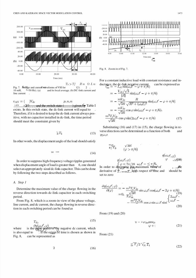
From the simulation waveforms shown in Fig. 7(a),12 and 3 can be found. During the time period ,
7/30/2019 Space Vector Modulation Control of an AC–DC–AC061
http://slidepdf.com/reader/full/space-vector-modulation-control-of-an-acdcac061 4/9
CHEN AND KAZERANI: SPACE VECTOR MODULATION CONTROL 1473
Fig. 7. Voltage and current waveforms of VSI for T > T = 12 ( R = 2 , L =
10 mH, f = 50 Hz). (a) v and its local average. (b) DC-link current andline current
i
.
2/3 and the switch state ( ) given by Table I
exists. In this switch state, the dc-link current will equal to .
Therefore, if it is desired to keep the dc-link current always pos-
itive, with no capacitor installed in dc-link, the time period
should meet the constraint given by
(13)
In other words, the displacement angle of the load should satisfy
(14)
In order to suppress high-frequency voltage ripples generated
when displacement angle of load is greater than 6, one should
select an appropriately-sized dc-link capacitor. This can be done
by following the two steps described as follows.
A. Step 1
Determine the maximum value of the charge flowing in the
reverse direction towards dc-link capacitor in each switching
period.
From Fig. 8, which is a zoom-in view of the phase voltage,
line current, and dc current, the charge flowing in reverse direc-
tion in each switching period can be found as
(15)
where is the pulse width of the negative dc current, which
is also equal to . If the origin of time is chosen as shown in
Fig. 8, can be represented as
(16)
Fig. 8. Zoom-in of Fig. 7.
For a constant inductive load with constant resistance and in-
ductance, the dc-link negative current can be expressed as
(17)
Substituting (16) and (17) in (15), the charge flowing in re-
verse direction can be determined as a function of both and
(18)
In order to determine the maximum value of , the
derivative of with respect to time and should be
set to zero
(19)
(20)
From (19) and (20)
(21)
From (21)
(22)
7/30/2019 Space Vector Modulation Control of an AC–DC–AC061
http://slidepdf.com/reader/full/space-vector-modulation-control-of-an-acdcac061 5/9
1474 IEEE TRANSACTIONS ON POWER ELECTRONICS, VOL. 21, NO. 5, SEPTEMBER 2006
Substituting (22) in (18), the maximum value of charge for a
constant inductive load can be found as
(23)
For inductive loads corresponding to 6 18,from (19)
(24)
Substituting (24) into (18)
(25)
For a motor, it is more effective to calculate the charge using
rated power , rated voltage and load displacementpower factor (DPF). The line current magnitude and displace-
ment angle are
and the negative dc-link current is
(26)
From (15), (16), and (26), at 1, the charge for motor load
can be obtained as
(27)
It can be proven that if
(28)
has the maximum value of
(29)
B. Step 2
Determine the capacitance based on and permitted
peak-to-peak dc-link voltage ripple .
As mentioned earlier in the paper, the job of the dc-link ca-pacitor is to absorb the energy released by the load in the form of
negative dc-link current pulses and the capacitor should be de-
signed based on the permitted peak-to-peak ripple on the dc-link
voltage. The capacitance of the dc-link capacitor can be related
to the maximum charge and the permitted peak-to-peak
dc-link voltage ripple , through the following expres-
sion:
(30)
For inductive load with constant resistance and inductance,
from (23), (24), and (30), the reduced capacitance needed in the
dc-link can be determined as
(31)
(32)
where .
For motor load, from (29) and (30), the reduced capacitance
needed in the dc-link can be determined as
(33)
Equation (33) implies that the reduced dc-link capacitor can be
used in cases where the motor displacement power factor does
not vary in a wide range and does not assume very low values,
such as near-zero values which happen at low- and no-load con-
ditions. The smaller the power factor that is allowed, the larger
the capacitance that has to be used.
V. SIMULATION RESULTS
In this section, the simulation results obtained from PSIMsimulation software for the proposed method are presented. The
following parameters have been used in the simulation of the
system shown in Fig. 6.
Source: three-phase, 60 Hz, 200 V (line-to-line, RMS).
DC-link capacitor: 30 F.
Low-pass filter: 796 Hz.
SVPWM controller: 6.2, 40 Hz, 0,
8 kHz.
The induction motor and mechanical load parameters are listedin Table II.
7/30/2019 Space Vector Modulation Control of an AC–DC–AC061
http://slidepdf.com/reader/full/space-vector-modulation-control-of-an-acdcac061 6/9
CHEN AND KAZERANI: SPACE VECTOR MODULATION CONTROL 1475
TABLE II
INDUCTION MOTOR AND MECHANICAL LOAD PARAMETERS
USED IN SIMULATIONS
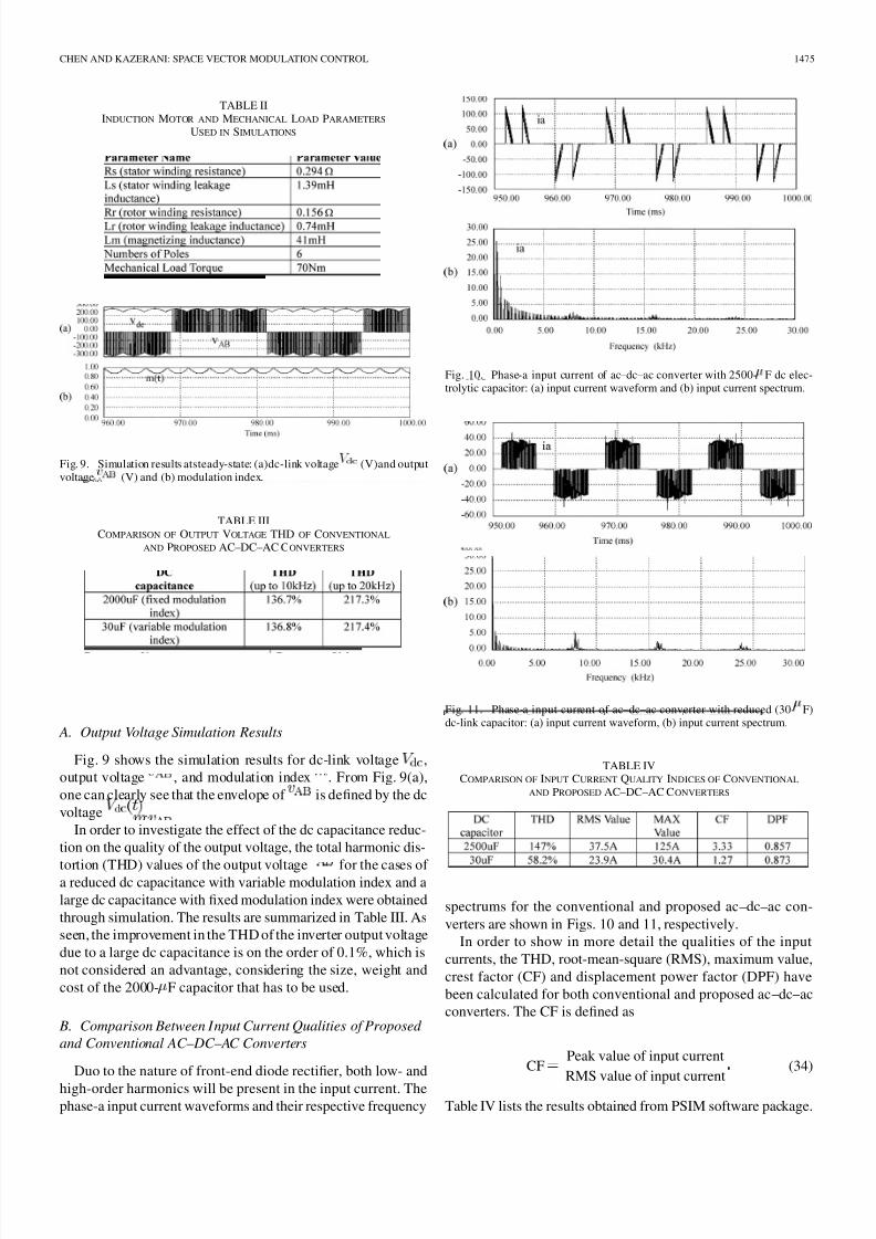
Fig. 9. Simulation results atsteady-state: (a)dc-link voltage V (V)and outputvoltage
v
(V) and (b) modulation index.
TABLE III
COMPARISON OF OUTPUT VOLTAGE THD OF CONVENTIONAL
AND PROPOSED AC–DC–AC CONVERTERS
A. Output Voltage Simulation Results
Fig. 9 shows the simulation results for dc-link voltage ,
output voltage , and modulation index . From Fig. 9(a),
one can clearly see that the envelope of is defined by the dc
voltage .
In order to investigate the effect of the dc capacitance reduc-
tion on the quality of the output voltage, the total harmonic dis-
tortion (THD) values of the output voltage for the cases of a reduced dc capacitance with variable modulation index and a
large dc capacitance with fixed modulation index were obtained
through simulation. The results are summarized in Table III. As
seen, the improvement in the THD of the inverter output voltage
due to a large dc capacitance is on the order of 0.1%, which is
not considered an advantage, considering the size, weight and
cost of the 2000- F capacitor that has to be used.
B. Comparison Between Input Current Qualities of Proposed
and Conventional AC–DC–AC Converters
Duo to the nature of front-end diode rectifier, both low- and
high-order harmonics will be present in the input current. Thephase-a input current waveforms and their respective frequency
Fig. 10. Phase-a input current of ac–dc–ac converter with 2500- F dc elec-trolytic capacitor: (a) input current waveform and (b) input current spectrum.
Fig. 11. Phase-a input current of ac–dc–ac converter with reduced (30- F)dc-link capacitor: (a) input current waveform, (b) input current spectrum.
TABLE IVCOMPARISON OF INPUT CURRENT QUALITY INDICES OF CONVENTIONAL
AND PROPOSED AC–DC–AC CONVERTERS
spectrums for the conventional and proposed ac–dc–ac con-
verters are shown in Figs. 10 and 11, respectively.
In order to show in more detail the qualities of the input
currents, the THD, root-mean-square (RMS), maximum value,
crest factor (CF) and displacement power factor (DPF) have
been calculated for both conventional and proposed ac–dc–ac
converters. The CF is defined as
CFPeak value of input current
RMS value of input current(34)
Table IV lists the results obtained from PSIM software package.
7/30/2019 Space Vector Modulation Control of an AC–DC–AC061
http://slidepdf.com/reader/full/space-vector-modulation-control-of-an-acdcac061 7/9
1476 IEEE TRANSACTIONS ON POWER ELECTRONICS, VOL. 21, NO. 5, SEPTEMBER 2006
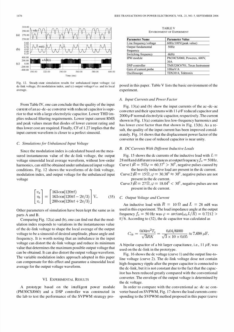
Fig. 12. Steady-state simulation results for unbalanced input voltage: (a)dc-link voltage, (b) modulation index, and (c) output voltage
v
and its local
average.
From Table IV, one can conclude that the quality of the input
current of an ac–dc–ac converter with reduced capacitor is supe-
rior to that with a large electrolytic capacitor. Lower THD im-
plies reduced filtering requirements. Lower input current RMS
and peak values mean that diodes of lower current rating and
thus lower cost are required. Finally, CF of 1.27 implies that the
input current waveform is closer to a perfect sinusoid.
C. Simulations for Unbalanced Input Voltage
Since the modulation index is calculated based on the mea-
sured instantaneous value of the dc-link voltage, the output
voltage sinusoidal local average waveform, without low-order
harmonics, can still be obtained under unbalanced input voltage
conditions. Fig. 12 shows the waveforms of dc-link voltage,
modulation index, and output voltage for the unbalanced inputvoltage
(35)
Other parameters of simulation have been kept the same as in
parts A and B.
Comparing Fig. 12(a) and (b), one can find out that the mod-
ulation index responds to variations in the instantaneous value
of the dc-link voltage to shape the local average of the output
voltage to be a sinusoid of desired amplitude, phase angle andfrequency. It is worth noting that an imbalance in the input
voltage can distort the dc-link voltage and reduce its minimum
value that determines the maximum possible output voltage that
can be obtained. It can also distort the output voltage waveform.
The variable modulation index approach adopted in this paper
can compensate for this effect and guarantee a sinusoidal local
average for the output voltage waveform.
VI. EXPERIMENTAL RESULTS
A prototype based on the intelligent power module
(PM30CSJ060) and a DSP controller was constructed inthe lab to test the performance of the SVPWM strategy pro-
TABLE V
ENVIRONMENT OF EXPERIMENT
posed in this paper. Table V lists the basic environment of the
experiment.
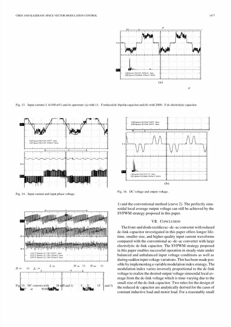
A. Input Currents and Power Factor
Fig. 13(a) and (b) show the input currents of the ac–dc–ac
converter and their spectrums with 11- F reduced capacitor and
2000- F normal electrolytic capacitor, respectively. The currentshown in Fig. 13(a) contains less low-frequency harmonics and
has lower crest factor than that shown in Fig. 13(b). As a re-
sult, the quality of the input current has been improved consid-
erately. Fig. 14 shows that the displacement power factor of the
converter in the case of reduced capacitor is near unity.
B. DC Currents With Different Inductive Loads
Fig. 15 shows the dc currents of the inductive load with
28 mHand different resistances at outputfrequency 50Hz.
Curve 1 ) 5 60.37 30 , negative pulses caused by
the heavily inductive load are present in the dc current.
Curve 2 ) 15 , 30.38 30 , negative pulses are notpresent in the dc current.
Curve 3 ) 27 , 18.04 30 , negative pulses are not
present in the dc current.
C. Output Voltage and Current
An inductive load with 10 and 28 mH was
used in this experiment. The load impedance angle at the output
frequency 50 Hz was 0.7212
6. According to (32), the dc capacitor was calculated as
A bipolar capacitor of a bit larger capacitance, i.e., 11 F, was
used on the dc-link in the prototype.
Fig. 16 shows the dc voltage (curve 1) and the output line-to-
line voltage (curve 2). The dc-link voltage dose not contain
high-frequency ripple after the proper capacitor is connected to
the dc-link, but it is not constant due to the fact that the capac-
itor has been reduced greatly compared with the conventional
converter. The envelope of the output voltage is determined by
the dc voltage.
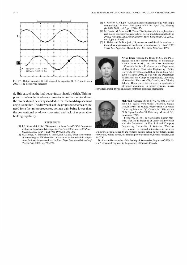
In order to compare with the conventional ac–dc–ac con-
verter based on SVPWM, Fig. 17 shows the load currents corre-sponding to the SVPWM method proposed in this paper (curve
7/30/2019 Space Vector Modulation Control of an AC–DC–AC061
http://slidepdf.com/reader/full/space-vector-modulation-control-of-an-acdcac061 8/9
CHEN AND KAZERANI: SPACE VECTOR MODULATION CONTROL 1477
Fig. 13. Input current (1 A/100 mV) and its spectrum: (a) with 11-
F reduced dc bipolar capacitor and (b) with 2000-
F dc electrolytic capacitor.
Fig. 14. Input current and input phase voltage.
Fig. 15. DC currents withL =
28 mH and 1)R =
5
, 2)R =
15
, and 3)R =
27
atf =
50 Hz.
Fig. 16. DC voltage and output voltage.
1) and the conventional method (curve 2). The perfectly sinu-
soidal local average output voltage can still be achieved by the
SVPWM strategy proposed in this paper.
VII. CONCLUSION
The front-end diode rectifierac–dc–ac converter with reduceddc-link capacitor investigated in this paper offers longer life-
time, smaller size, and higher-quality input current waveforms
compared with the conventional ac–dc–ac converter with large
electrolytic dc-link capacitor. The SVPWM strategy proposed
in this paper enables successful operation in steady-state under
balanced and unbalanced input voltage conditions as well as
during sudden input voltage variations. This has been made pos-
sible by implementing a variable modulation index strategy. The
modulation index varies inversely proportional to the dc-link
voltage to realize the desired output voltage sinusoidal local av-
erage from the dc-link voltage which is time-varying due to the
small size of the dc-link capacitor. Two rules for the design of
the reduced dc capacitor are analytically derived for the cases of constant inductive load and motor load. For a reasonably small
7/30/2019 Space Vector Modulation Control of an AC–DC–AC061
http://slidepdf.com/reader/full/space-vector-modulation-control-of-an-acdcac061 9/9
1478 IEEE TRANSACTIONS ON POWER ELECTRONICS, VOL. 21, NO. 5, SEPTEMBER 2006
Fig. 17. Output currents: 1) with reduced dc capacitor (11- F) and 2) with2000- F dc electrolytic capacitor.
dc-link capacitor, the load power factor should be high. This im-plies that when the ac–dc–ac converter is used as a motor drive,
the motor should be always loaded so that the load displacement
angle is smaller. The drawbacks of the proposed scheme are the
need for a fast microprocessor, voltage gain being lower than
the conventional ac–dc–ac converter, and lack of regenerative
braking capability.
REFERENCES
[1] J.S. Kim and S.K.Sul, “New control scheme for AC-DC-ACconverter
without dc link electrolyticcapacitor,” in Proc. 24thAnnu. IEEEPower Electron. Spec. Conf. (PESC ’93), 1993, pp. 300–306.
[2] M. Muroya, K. Shinohara, K. Iimori, and H. Sako, “Four-step commu-
tation strategy of PWM rectifier of converter without dc link compo-nents for induction motor drive,” in Proc. Elect. Machines Drives Conf.(EMDC ’01), 2001, pp. 770–772.
[3] L. Wei and T. A. Lipo, “A novel matrix converter topology with simplecommutation,” in Proc. 36th Annu. IEEE Ind. Appl. Soc. Meeting(IAS ’01), 2001, vol. 3, pp. 1749–1754.
[4] M. Jussila, M. Salo, and H. Tuusa, “Realization of a three-phase indi-rect matrix converter with an indirect vector modulation method,” inProc. 34th Annu. IEEE Power Electron. Spec. Conf. (PESC ’03), 2003,vol. 2, pp. 689–694.
[5] L. Huber and D. Borojevic, “Space vector modulated three-phase to
three-phase matrix converter with input power factor correction,” IEEE Trans. Ind. Appl., vol. 31, no. 6, pp. 1234–1246, Nov./Dec. 1995.
Xiyou Chen received the B.Sc., M.Sc., and Ph.D.degrees from the Harbin Institute of Technology,Harbin, China, in 1982, 1985, and 2000, respectively.
Currently, he is a Professor in the Departmentof Electrical and Electronics Engineering, DalianUniversity of Technology, Dalian, China. From April2004 to March 2005, he was with the Departmentof Electrical and Computer Engineering, Universityof Waterloo, Waterloo, ON, Canada, as a Visiting
Scholar. His research interests are in applicationsof power electronics in power systems, matrix
converters, motor drives, and chaos control in electrical engineering.
Mehrdad Kazerani (S’88–M’96–SM’02) receivedthe B.Sc. degree from Shiraz University, Shiraz,Iran, in 1980, the M.Eng. degree from ConcordiaUniversity, Montreal, QC, Canada, in 1990, and thePh.D. degree from McGill University, Montreal, QC,Canada, in 1995.
From 1982 to 1987, he was with the Energy Min-istry, Iran. He is presently an Associate Professorwith the Department of Electrical and ComputerEngineering, University of Waterloo, Waterloo,
ON, Canada. His research interests are in the areasof power electronic circuits and systems design, active power filters, matrixconverters, pulsed power, distributed power generation, hybrid vehicles, and
FACTS.Dr. Kazerani is a member of the Society of Automotive Engineers (SAE). He
is a Professional Engineer in the province of Ontario, Canada.