Embed Size (px)
Citation preview
53
Chapter – 4
Hybrid Pulse Width Modulation Algorithm forVector Controlled Induction Motor Drive
4.1 Introduction:
The induction motors have been widely used in the industrial
applications to convert the electric power to mechanical power. Hence,
these are also known as workhorse of the industry. With the advent of
Field Oriented Control (FOC) algorithm, the induction motor drives offer
fast transient response as well as independent control on flux and
torque, which is similar to that of the separately excited DC motor drive.
The FOC is also known as vector control. The vector control is referred
for controlling both amplitude and phase angle of the stator current. In
the case of vector controlled induction motor drives, the rotor flux
oriented control is usually employed although it is possible to implement
stator flux oriented control. The stator or rotor flux linkages of the
induction motors are necessary for the vector control. In terms of the
methods of obtaining the unit vectors, the FOC drive systems are
classified into two categories, the direct field oriented control (DFOC) and
the indirect field oriented control (IFOC) algorithms. In DFOC, the unit
vectors are generated from the flux quantities, which are directly
54
measured by using Hall-effect sensors, etc. Whereas in the IFOC
algorithm, the space angle of the flux linkage is obtained as the sum of
the monitored rotor angle (corresponding to the rotor speed) and the
computed reference value of the slip angle (corresponding to the slip
frequency). The IFOC algorithms are receiving wide attention in many
applications. But, the indirect vector control algorithm uses hysteresis
band type current controllers for the generation of gating signals. This
causes increased ripple in steady state currents and variable switching
frequency operation. To overcome the above said problems, space vector
pulse width modulation (SVPWM) algorithm has been developed for
vector controlled induction motor drive. However, the complexity involved
in conventional SVPWM algorithm is more due to the calculation of
angle, sector and reference voltage vector. Moreover, the conventional
SVPWM algorithm gives inferior performance at higher modulation
indices. As the CSVPWM is a continuous PWM (CPWM), it gives more
switching losses.
This chapter presents a novel hybrid PWM (HPWM) algorithm that
uses the SVPWM and various discontinuous PWM (DPWM) algorithms.
The proposed HPWM algorithm uses the concept of imaginary switching
times which are derived from instantaneous phase voltages. This
algorithm does not require angle and sector information and hence
reduces the complexity of the algorithm. Also, the proposed HPWM
algorithm decreases total harmonic distortion (THD in the stator current)
55
and switching losses of the inverter at all modulation indices. Moreover,
this chapter presents a detailed switching loss analysis of various PWM
algorithms and the minimum switching loss PWM algorithms for
induction motor drives.
4.2 Principle of Vector Control:
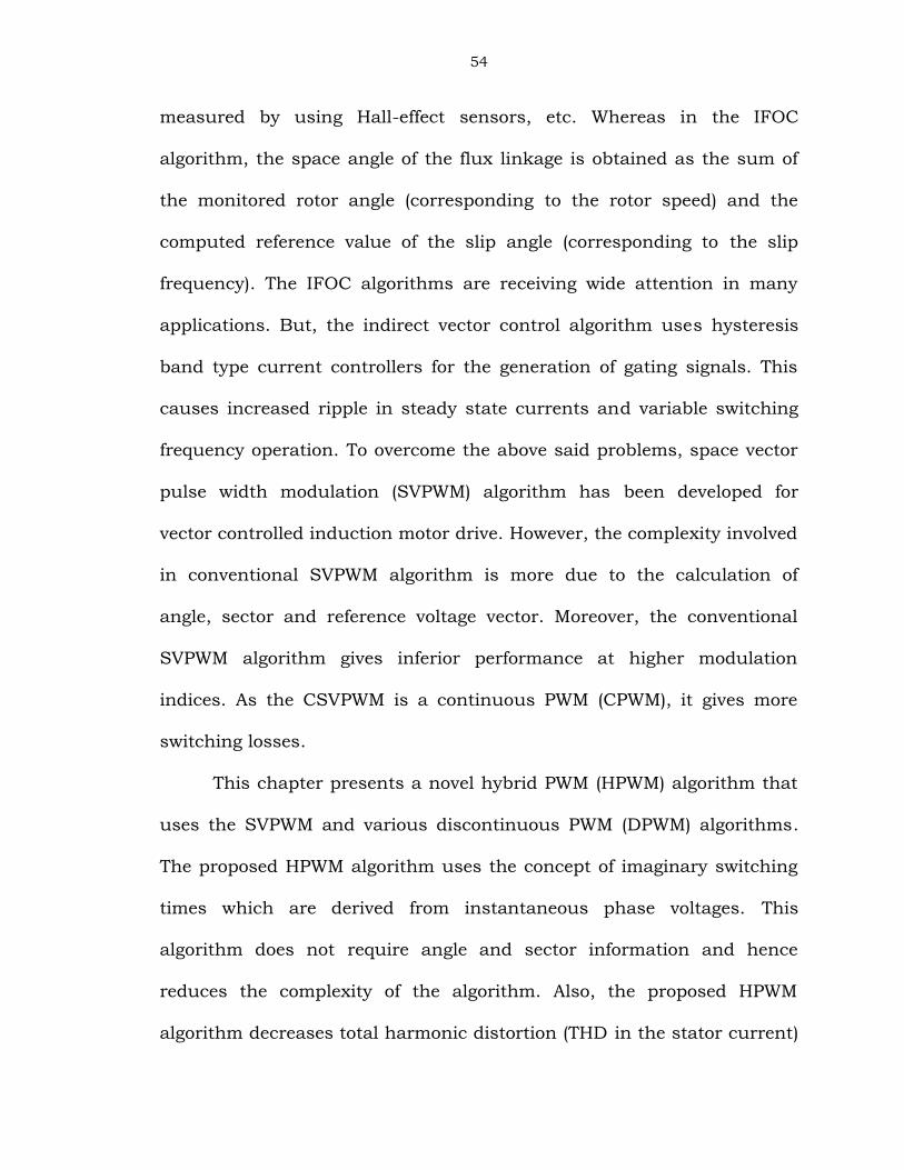
Traditionally, separately excited DC motors are popular in variable
speed applications. Because, in the separately excited DC machine the
armature and field currents can be controlled independently. The
simplified DC machine model can be represented as shown in Fig. 4.1.
Fig. 4.1 Simplified DC machine model
Due to the electromagnetic interaction between the field flux and the
armature MMF, the electromagnetic torque can be generated, which is
proportional to the armature current. The expression for electromagnetic
torque can be finally written as
afte IkT (4.1)
From the above discussion it can be concluded that to achieve fast
torque control the armature current should be independently controlled,
while keeping the field current as constant. But in induction motors, this
_
+
Va
Ia
Nf
If
_
Vf
+
56
requirement has to be achieved through external control and the process
is much more complex than that of DC machines.
The first major breakthrough in the area of high performance
induction motors is the discovery of vector control (VC) (also known as
field oriented control (FOC)) by F. Blaschke in 1972[2]. Blaschke
examined how field orientation occurs naturally in a separately excited
DC motor. In the DC motor, the armature and field current are always
perpendicular to each other. Similar condition can be obtained in an
induction motor by using vector control algorithm. Vector control
algorithm provides a method of decoupling the two components of stator
current, one producing the torque and the other producing flux. Hence,
this algorithm gives independent control of torque and flux.
As the steady state operation is also the special case of the
transient analysis by assuming the derivative terms to be zero, in
variable speed drive applications, the study of transient analysis is most
important. Hence, it is very useful to derive the vector control of
induction motor using the transient model. The phasor diagram of the
stator voltages, currents and rotor flux is shown in Fig. 4.2. The rotor
flux linkage vector r is supposed to have q- and d-axis components as
the voltages and currents have. But in vector control algorithm, it is
possible to align the whole phasor with the synchronous reference frame.
Hence, the analysis becomes simple and the field is represented by a
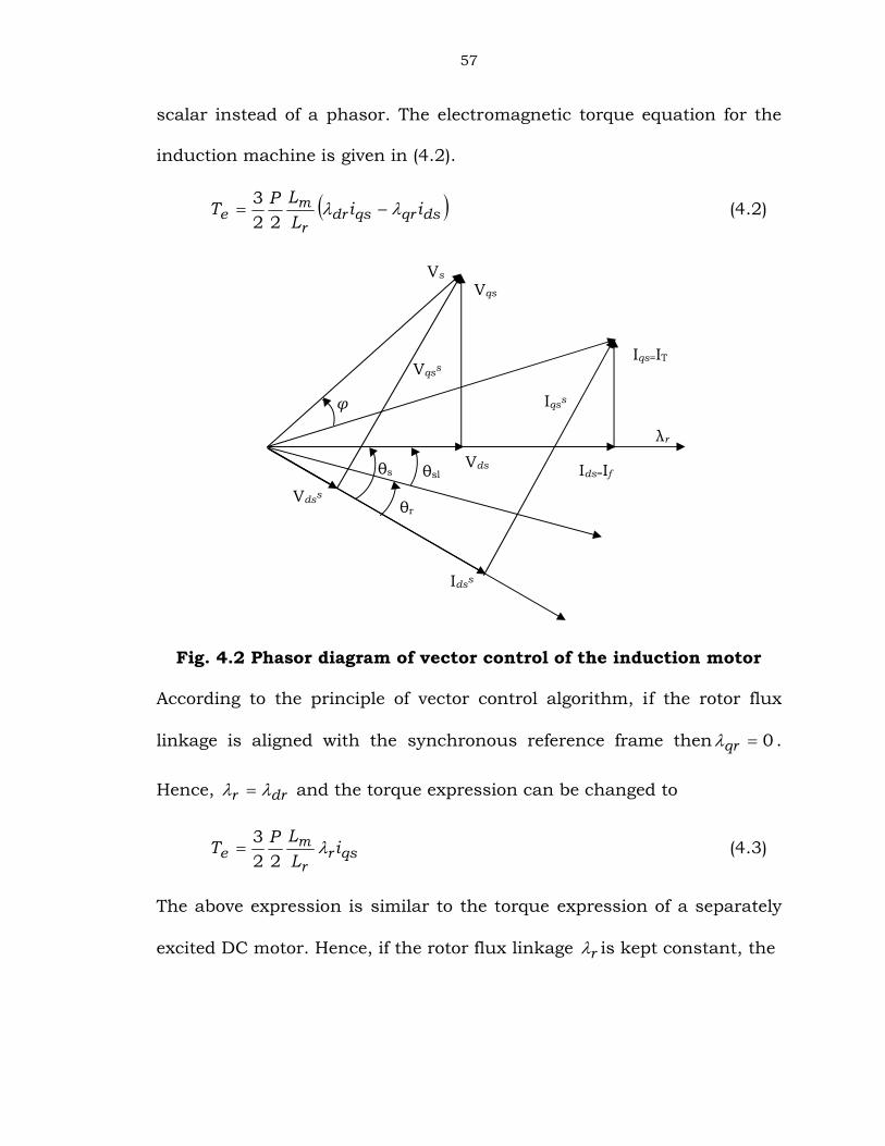
57
scalar instead of a phasor. The electromagnetic torque equation for the
induction machine is given in (4.2).
dsqrqsdrr
me ii
LLPT
223 (4.2)
Fig. 4.2 Phasor diagram of vector control of the induction motor
According to the principle of vector control algorithm, if the rotor flux
linkage is aligned with the synchronous reference frame then 0qr .
Hence, drr and the torque expression can be changed to
qsrr
me i
LLPT
223 (4.3)
The above expression is similar to the torque expression of a separately
excited DC motor. Hence, if the rotor flux linkage r is kept constant, the
φ
θsVdsθsl
θr
λr
Iqs=IT
Idss
Iqss
Vdss
Vqss
VqsVs
Ids=If

58
output torque will be proportional to the q-axis stator current in the
synchronous reference frame. Apparently r and qsi are not independent.
The stator and rotor flux linkages and the torque are coming from the AC
voltages applied to the stator of the induction motor and the current
generated. So instantaneous decoupling and independent control of the
rotor flux linkages and stator currents are the two most important issues
to deal with. Since the vector control is basically in the synchronous
reference frame, the instant angle for the synchronous reference frame
with respect to the stator reference frame needs to be determined first.
According to Fig. 4.2, this angle is the position angle of the rotor flux
linkage vector ( s ). If the rotor flux linkage vector position angle is
known, all variables can be transformed into the synchronous reference
frame, in which the quantities after transformation become DC
quantities [2-3].
Based on the measure of rotor flux linkage position angle, the
vector control schemes can be classified into two categories: direct vector
control (or direct field oriented control (DFOC)) and indirect vector
control (or indirect field oriented control (IFOC)). In the direct vector
control scheme, the angle is determined from the flux measurements
using Hall sensors or flux sensing windings. While in the indirect vector
control scheme, the angle is computed from the measured rotor position
angle and the slip angle. The relationship between these angles is given
in (4.4).
59
dtdt sslrslrs (4.4)
In order to get the s for the DFOC scheme, the additional sensors or
windings need to be installed inside the induction motor, which need
special design for different type of induction motors and introduce a
potential fault condition. So the more popular control scheme is the IFOC
scheme, in which the rotor speed is measured using rotor position or
speed sensors. The slip frequency is calculated and then the position
angle of the rotor flux linkage vector is calculated using (4.4). In the
normal operation, the rotor speed is always important and measured,
which means the IFOC scheme will not increase the cost at all[2.-3]. The
IFOC scheme for induction motor is derived in detail in the following
section.
4.3 Indirect Vector Control of Induction Motor:
In the indirect vector control of induction motor, a VSI is supposed
to drive the motor so that the slip frequency can be changed according to
the particular requirement. Assuming the rotor speed is measured, and
then the slip speed is derived in the feed-forward manner. The rotor
voltage equations of the induction motor can be given as:
0
0
drslqrrqr
qrsldrrdr
iRdtd
iRdtd
(4.5)
The rotor flux linkage expressions can be written as
60
qsmqrrqr
dsmdrrdriLiLiLiL
(4.6)
From (4.6), the rotor currents can be written as
qsr
mqr
rqr
dsr
mdr
rdr
iLL
Li
iLL
Li
1
1
(4.7)
By substituting (4.7) in (4.5), (4.5) can be modified as
0
0
drslqsr
rmqr
r
rqr
qrsldsr
rmdr
r
rdr
iLRL
LR
dtd
iLRL
LR
dtd
(4.8)
For decoupling control, it is desirable that the rotor flux is aligned onto
the d-axis of the synchronously rotating reference frame, then
rdrqr
qr dtd
and00 (4.9)
By substituting (4.9) in (4.8), (4.8) can be modified as
qsrr
rmsl
dsmrr
r
r
iLRL
iLdtd
RL
(4.10)
If rotor flux is constant then the rotor flux linkage expression can be
written from (4.10) as
dsmr iL (4.11)
The block diagram of indirect vector controlled induction motor drive can
be shown as in Fig. 4.3. This shows how the rotor flux linkage position
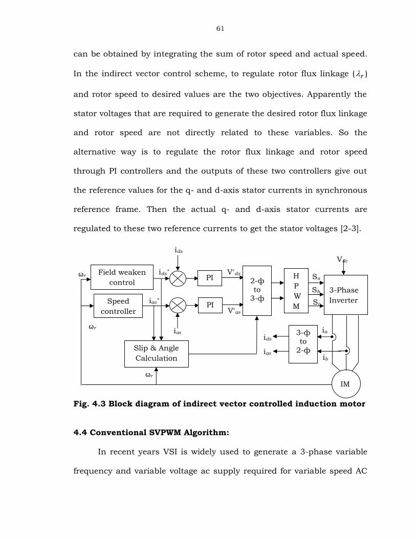
61
ids
can be obtained by integrating the sum of rotor speed and actual speed.
In the indirect vector control scheme, to regulate rotor flux linkage ( r )
and rotor speed to desired values are the two objectives. Apparently the
stator voltages that are required to generate the desired rotor flux linkage
and rotor speed are not directly related to these variables. So the
alternative way is to regulate the rotor flux linkage and rotor speed
through PI controllers and the outputs of these two controllers give out
the reference values for the q- and d-axis stator currents in synchronous
reference frame. Then the actual q- and d-axis stator currents are
regulated to these two reference currents to get the stator voltages [2-3].
Fig. 4.3 Block diagram of indirect vector controlled induction motor
4.4 Conventional SVPWM Algorithm:
In recent years VSI is widely used to generate a 3-phase variable
frequency and variable voltage ac supply required for variable speed AC
Vdc
Sc
Sb
Sa
ib
iaids
iqs
V*qs
V*ds
iqs
iqs*
ids*
ωr
ωr
Slip & AngleCalculation
3-PhaseInverter
3-фto
2-ф
Speedcontroller
PI
2-фto
3-ф
HPWM
Field weakencontrol PI
IM
ωr
62
drives. The ac voltage is defined by two characteristics, namely amplitude
and frequency. Hence, it is essential to work out an algorithm that
permits control over both of these quantities. PWM controls the average
output voltage over a sufficiently small period called sampling period or
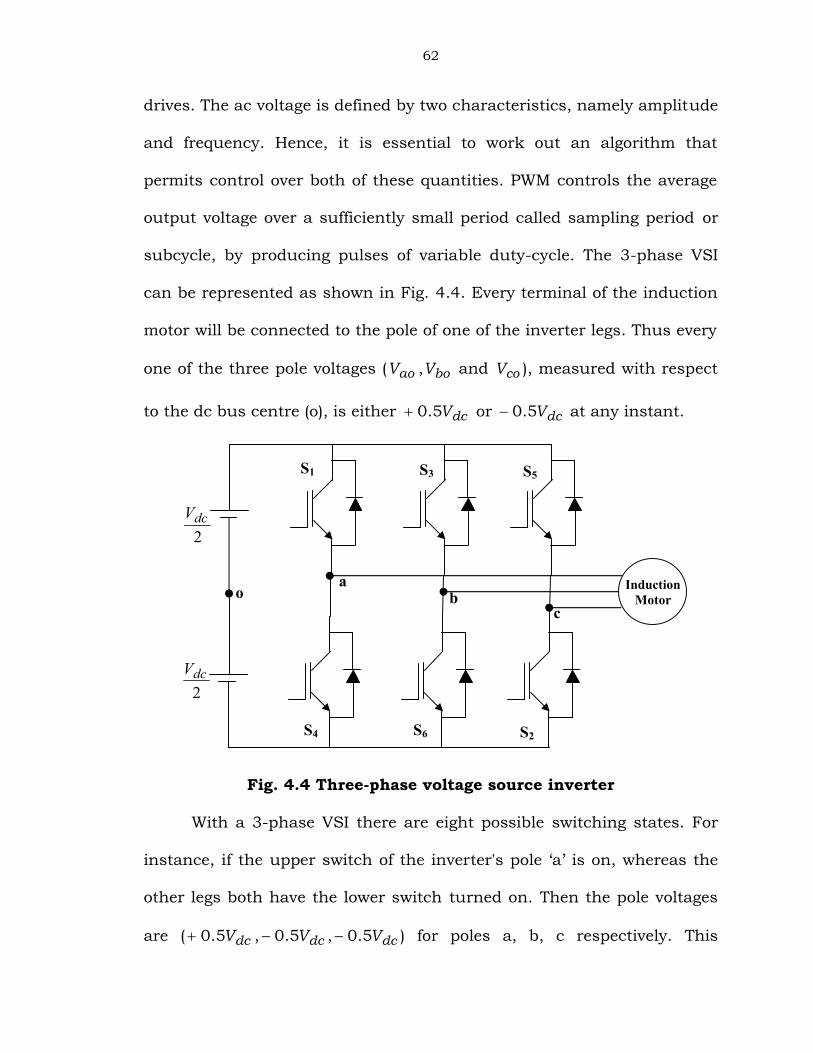
subcycle, by producing pulses of variable duty-cycle. The 3-phase VSI
can be represented as shown in Fig. 4.4. Every terminal of the induction
motor will be connected to the pole of one of the inverter legs. Thus every
one of the three pole voltages ( aoV , boV and coV ), measured with respect
to the dc bus centre (o), is either dcV5.0 or dcV5.0 at any instant.
Fig. 4.4 Three-phase voltage source inverter
With a 3-phase VSI there are eight possible switching states. For
instance, if the upper switch of the inverter's pole ‘a’ is on, whereas the
other legs both have the lower switch turned on. Then the pole voltages
are ( dcV5.0 , dcV5.0 , dcV5.0 ) for poles a, b, c respectively. This
o
2dcV
2dcV
ab
c
S4
S1 S3 S5
S6 S2
InductionMotor
63
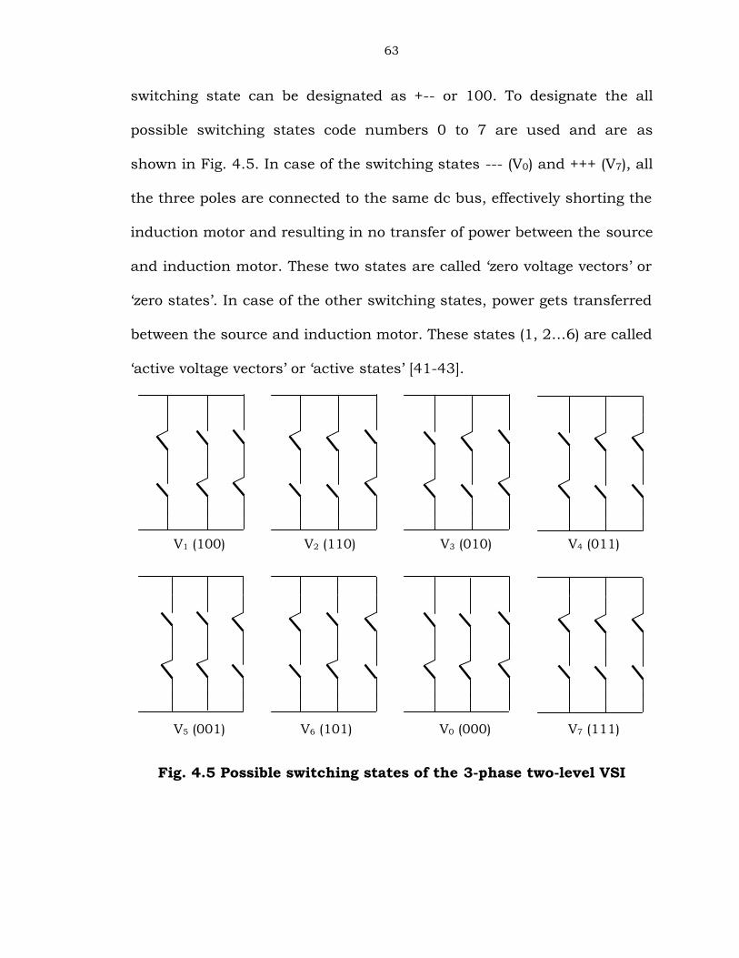
switching state can be designated as +-- or 100. To designate the all
possible switching states code numbers 0 to 7 are used and are as
shown in Fig. 4.5. In case of the switching states --- (V0) and +++ (V7), all
the three poles are connected to the same dc bus, effectively shorting the
induction motor and resulting in no transfer of power between the source
and induction motor. These two states are called ‘zero voltage vectors’ or
‘zero states’. In case of the other switching states, power gets transferred
between the source and induction motor. These states (1, 2…6) are called
‘active voltage vectors’ or ‘active states’ [41-43].
Fig. 4.5 Possible switching states of the 3-phase two-level VSI
V1 (100) V2 (110) V3 (010) V4 (011)
V5 (001) V6 (101) V0 (000) V7 (111)
64
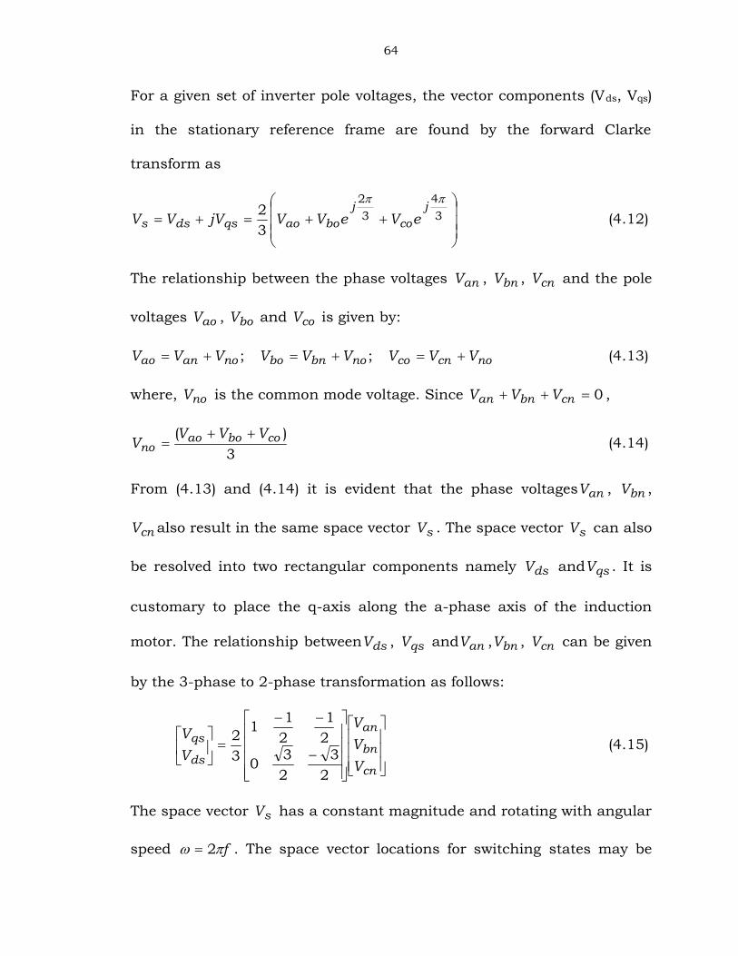
For a given set of inverter pole voltages, the vector components (Vds, Vqs)
in the stationary reference frame are found by the forward Clarke
transform as
3
43
2
32
jco
jboaoqsdss eVeVVjVVV (4.12)
The relationship between the phase voltages anV , bnV , cnV and the pole
voltages aoV , boV and coV is given by:
nocnconobnbonoanao VVVVVVVVV ;; (4.13)
where, noV is the common mode voltage. Since 0 cnbnan VVV ,
3)( coboao
noVVV
V
(4.14)
From (4.13) and (4.14) it is evident that the phase voltages anV , bnV ,
cnV also result in the same space vector sV . The space vector sV can also
be resolved into two rectangular components namely dsV and qsV . It is
customary to place the q-axis along the a-phase axis of the induction
motor. The relationship between dsV , qsV and anV , bnV , cnV can be given
by the 3-phase to 2-phase transformation as follows:
cn
bn
an
ds
qs
VVV
VV
23
230
21
211
32 (4.15)
The space vector sV has a constant magnitude and rotating with angular
speed f 2 . The space vector locations for switching states may be
65
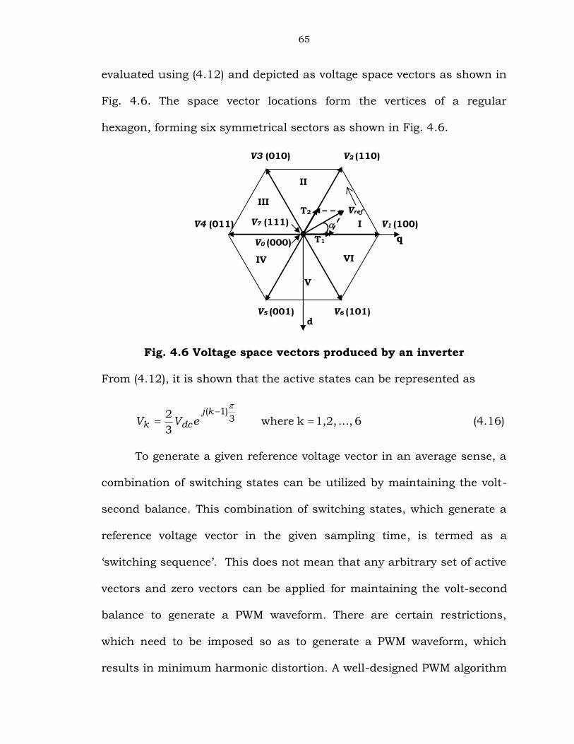
evaluated using (4.12) and depicted as voltage space vectors as shown in
Fig. 4.6. The space vector locations form the vertices of a regular
hexagon, forming six symmetrical sectors as shown in Fig. 4.6.
Fig. 4.6 Voltage space vectors produced by an inverter
From (4.12), it is shown that the active states can be represented as
6...,1,2,kwhere32 3
)1(
kj
dck eVV (4.16)
To generate a given reference voltage vector in an average sense, a
combination of switching states can be utilized by maintaining the volt-
second balance. This combination of switching states, which generate a
reference voltage vector in the given sampling time, is termed as a
‘switching sequence’. This does not mean that any arbitrary set of active
vectors and zero vectors can be applied for maintaining the volt-second
balance to generate a PWM waveform. There are certain restrictions,
which need to be imposed so as to generate a PWM waveform, which
results in minimum harmonic distortion. A well-designed PWM algorithm
Vref
MotorModel
V1 (100)
V2 (110)V3 (010)
V4 (011)
V5 (001) V6 (101)
V0 (000)
V7 (111) I
II
III
IV
V
VI
q
d
T1
T2
66
is one in which there are no pulses of opposite polarity in the line-to-line
voltage waveforms, that is, a line-to-line voltage must be either dcV or 0
and must not be dcV at any instant in the positive half-cycle, the
existence of which would lead to large ripple currents. Further, the
simultaneous switching of two phases must be avoided to utilize the
available switching frequency of the inverter efficiently. Hence, when the
reference voltage vector is within a given sector, the active states that can
be applied are only those two vectors, which form the boundaries of that
sector. The application of any other active states, results in a pulse of
opposite polarity.
The voltage vector refV in Fig. 4.6 represents the reference voltage
space vector or sample, corresponding to the desired value of the
fundamental components for the output phase voltages. It is obtained by
substituting the instantaneous values of the reference phase voltages,
sampled at regular time intervals in (4.12). The refV is sampled at equal
intervals of time, sT referred to as subcycle or sampling time period.
Different voltage vectors that can be produced by the inverter are applied
over different durations with in a subcycle such that the average vector
produced over the subcycle is equal to refV , both in terms of magnitude
and angle. It has been established that the vectors to be used to generate
any sample are the zero vectors and the two active vectors forming the
boundary of the sector in which the sample lies.
67
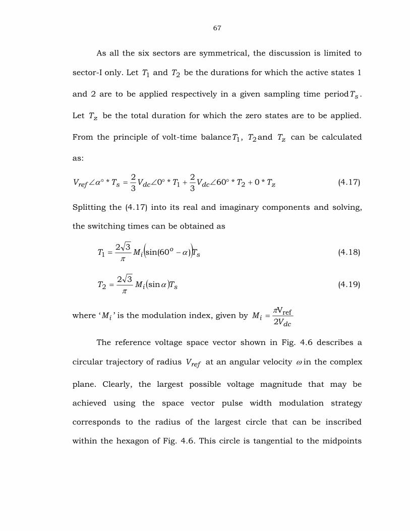
As all the six sectors are symmetrical, the discussion is limited to
sector-I only. Let 1T and 2T be the durations for which the active states 1
and 2 are to be applied respectively in a given sampling time period sT .
Let zT be the total duration for which the zero states are to be applied.
From the principle of volt-time balance 1T , 2T and zT can be calculated
as:
zdcdcsref TTVTVTV *0*6032*0
32* 21 (4.17)
Splitting the (4.17) into its real and imaginary components and solving,
the switching times can be obtained as
soi TMT )60sin(32
1
(4.18)
sin322 si TMT
(4.19)
where ‘ iM ’ is the modulation index, given bydc
i VM
2Vref
The reference voltage space vector shown in Fig. 4.6 describes a
circular trajectory of radius refV at an angular velocity in the complex
plane. Clearly, the largest possible voltage magnitude that may be
achieved using the space vector pulse width modulation strategy
corresponds to the radius of the largest circle that can be inscribed
within the hexagon of Fig. 4.6. This circle is tangential to the midpoints
68
of the lines connecting the ends of the active state vectors. The maximum
fundamental phase voltage that may be achieved is:
23
32
max dcref VV (4.20)
Then the corresponding maximum modulation index is given by
906.02
23
32*
max, dc
dci V
VM
(4.21)
As seen, the maximum peak fundamental magnitude that may be
obtained with the SVPWM algorithm is about 90.6% of the inverter
capacity. This represents a 15% increase in the maximum voltage
compared with sinusoidal PWM.
The total zero state time Tz may be divided in an arbitrary fashion
between the two zero states. A common solution is to divide Tz equally
between the two zero states V0 and V 7, that is
21 TTTT sZ (4.22)
Further, in the SVPWM method, the zero voltage vector time is
distributed symmetrically at the start and end of the subcycle in a
symmetrical manner. Moreover, to minimize the switching frequency of
the inverter, it is desirable that switching should take place in one phase
of the inverter only for a transition from one state to another. Thus,
SVPWM uses 0127-7210 in sector-I, 0327-7230 in sector-II and so on.
Fig. 4.7 shows a typical switching sequence when the reference voltage
vector is situated in first sector.
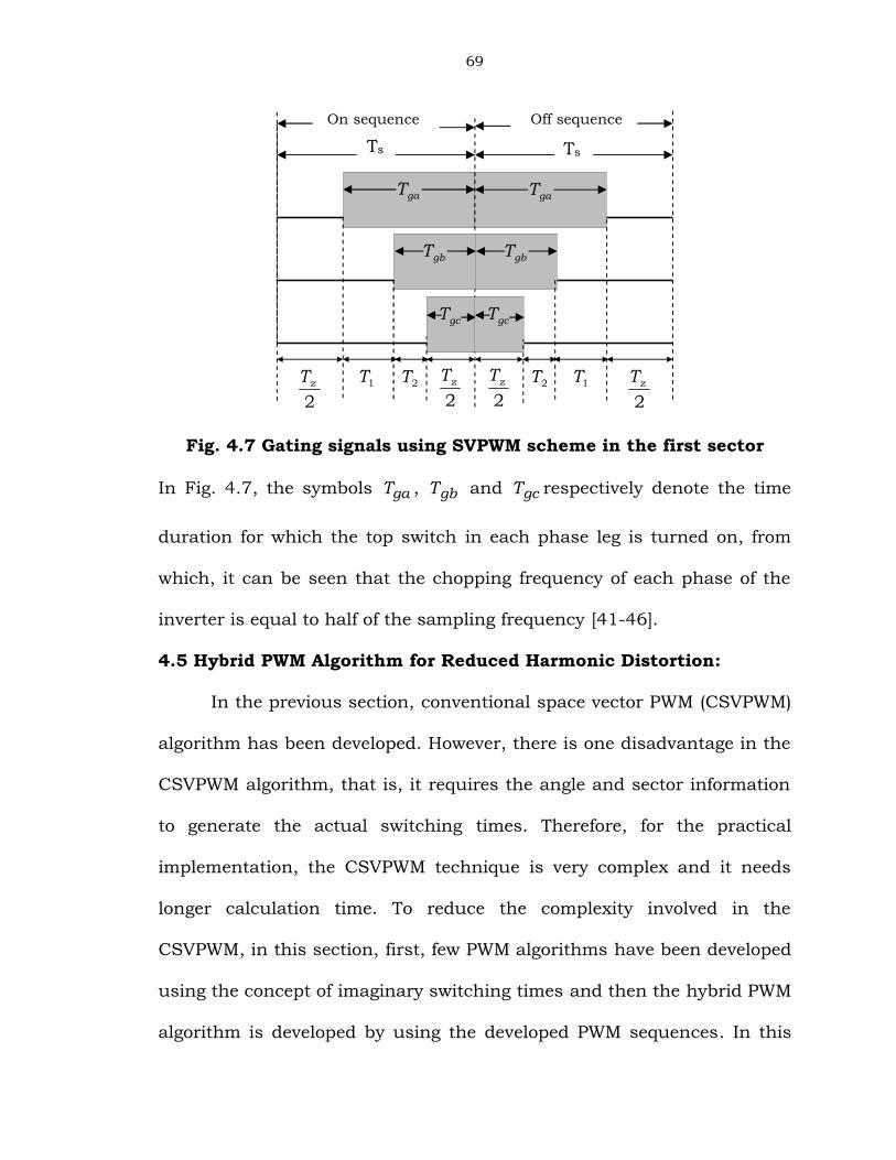
69
Fig. 4.7 Gating signals using SVPWM scheme in the first sector
In Fig. 4.7, the symbols gaT , gbT and gcT respectively denote the time
duration for which the top switch in each phase leg is turned on, from
which, it can be seen that the chopping frequency of each phase of the
inverter is equal to half of the sampling frequency [41-46].
4.5 Hybrid PWM Algorithm for Reduced Harmonic Distortion:
In the previous section, conventional space vector PWM (CSVPWM)
algorithm has been developed. However, there is one disadvantage in the
CSVPWM algorithm, that is, it requires the angle and sector information
to generate the actual switching times. Therefore, for the practical
implementation, the CSVPWM technique is very complex and it needs
longer calculation time. To reduce the complexity involved in the
CSVPWM, in this section, first, few PWM algorithms have been developed
using the concept of imaginary switching times and then the hybrid PWM
algorithm is developed by using the developed PWM sequences. In this
2zT
2zT
2zT
2zT
gaT gaT
gbTgbT
gcT gcT
On sequence Off sequence
Ts Ts
1T 1T2T 2T
70
approach, the actual switching times for each inverter leg are deduced
directly from the instantaneous phase voltages as a simple form.
4.5.1 Proposed Switching Sequences:
The proposed approach uses only the instantaneous reference phase
voltages to calculate switching times. This method does not depend on
the magnitude of the reference voltage space vector and its relative angle
with respect to the reference axis. By the d-q transformation theory, the
transformation from two-phase voltages to three-phase voltages can be
obtained from the stationary frame reference voltages as given in (4.23).
ds
qs
cn
bn
an
VV
VVV
23
21
23
21
01(4.23)
If the reference voltage vector lies in the first sector as shown in Fig. 4.6,
then the actual switching times can be deduced as follows [52, 73]:
bnanbndc
san
dc
s TTVVT
VVT
T 1 (4.23)
And cnbncndc
sbn
dc
s TTVVT
VVT
T 2 (4.24)
From the above expressions, the imaginary switching time periods
proportional to the instantaneous values of the reference phase voltages
are defined as
cndc
scnbn
dc
sbnan
dc
san V
VT
TVVT
TVVT
T
;; (4.25)
71
Thus, the active voltage vector switching times can be represented by the
time difference between the imaginary switching time periods. The
switching times cnbnan TTT and, could be negative when the
instantaneous reference voltages are negative. Hence, these times are
called as imaginary switching times. The active vector switching times
can be calculated in each sampling interval as follows:
Let),,(),,(),,(
cnbnanMid
cnbnanMin
cnbnanMax
TTTMidTTTTMinTTTTMaxT
(4.26)
where Max, Min and Mid are the nominal values used during the
sampling interval. The function ),,( cnbnan TTTMax selects the maximum
value among cnbnan TTT and, . Similarly ),,( cnbnan TTTMin selects the
minimum value and ),,( cnbnan TTTMid selects the middle value. Therefore
the active state times T1 and T2 may be expressed as [73]
MinMid
MidMaxTTTTTT
2
1 (4.27)
The effective time ( effT ) can be defined as the time between maxT and
minT and is given by sum of two active vector switching times. The
effective time means the time duration in which the effective voltage is
supplied to the motor terminals. The zero voltage vectors switching time
is calculated using (4.22). The CSVPWM algorithm employs equal
division of zero voltage vector time within a sampling time period.
However, by utilizing the freedom of zero state time division, various
72
discontinuous PWM (DPWM) algorithms can be generated. In the
proposed PWM sequences the zero state time will be shared between two
zero states as 0T for 0V and 7T for 7V respectively, and can be expressed
as [6]
zo
zoTkT
TkT)1(7
0
(4.28)
If 1and0,5.0ok , then CSVPWM, DPWMMAX and DPWMMIN can be
obtained respectively. When 0ok , any one of the phases is clamped to
positive DC bus for 120 degrees over a fundamental interval and
when 1ok , any one of the phases is clamped to negative DC bus for 120
degrees over a fundamental interval. Thus, in the first sector, CSVPWM
uses 0127-7210 sequence, DPWMMAX uses 721-127 sequence and
DPWMMIN uses 012-210 sequence. The switching sequences pertaining
to all six sectors for the above PWM algorithms are listed in Table 4.1.
Table 4.1 Switching sequences in all six sectors:
Sector CSVPWM DPWMMIN DPWMMAX
I 0127-7210 012-210 721-127
II 0327-7230 032-230 723-327
III 0347-7430 034-430 743-347
IV 0547-7450 054-450 745-547
V 0567-7650 056-650 765-567
VI 0167-7610 016-610 761-167
73
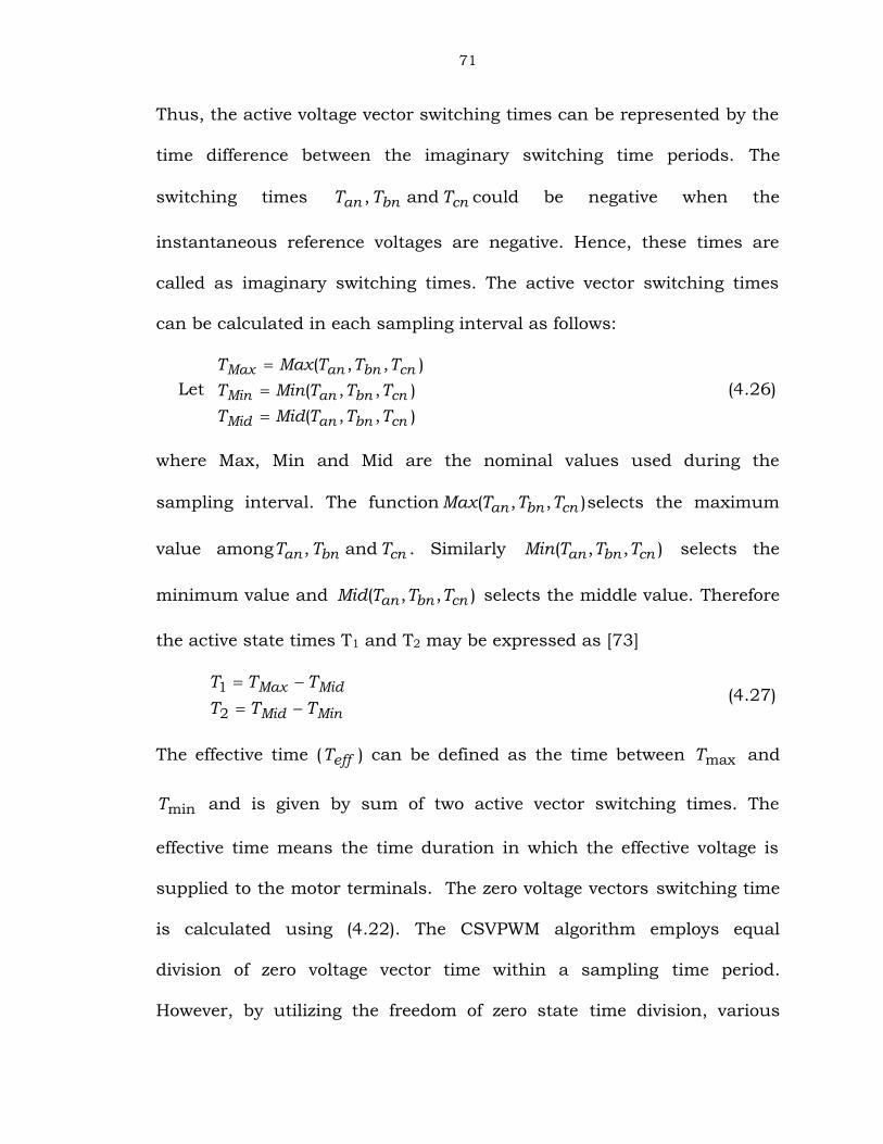
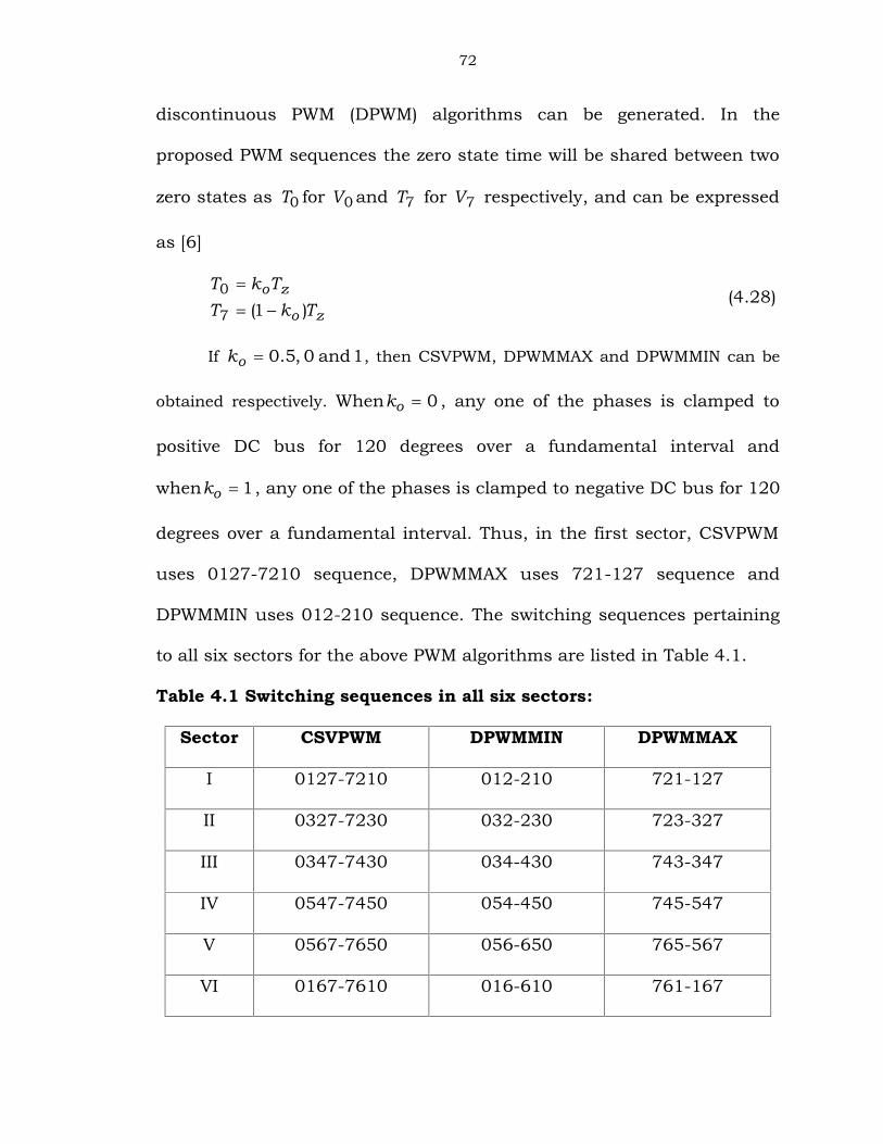
Various DPWM algorithms can be generated with step change of ok
between zero and one.
Fig. 4.8 Generation of DPWM0 method by varying the ok
Fig. 4.9 Generation of DPWM2 method by varying the ok
3V
1V
2V
4V
5V
1ok
0ok
1ok
0ok
6V
1ok
0ok
3V
1V
2V
4V
5V
0ok
1ok
0ok
1ok
6V
0ok
1ok
74
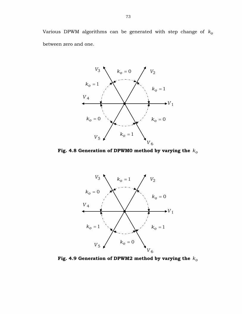
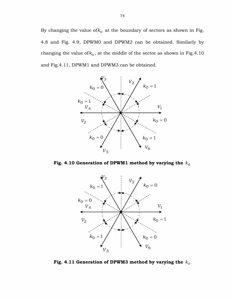
By changing the value of ok at the boundary of sectors as shown in Fig.
4.8 and Fig. 4.9, DPWM0 and DPWM2 can be obtained. Similarly by
changing the value of ok , at the middle of the sector as shown in Fig.4.10
and Fig.4.11, DPWM1 and DPWM3 can be obtained.
Fig. 4.10 Generation of DPWM1 method by varying the ok
Fig. 4.11 Generation of DPWM3 method by varying the ok
2V
1V
2V
4V
5V
00 k
00 k
10 k
10 k
00 k
3V
10 k
6V
2V
1V
2V
4V
5V
10 k
10 k
00 k
00 k
10 k
3V
00 k
6V
75
0 60 120 180 240 300 360-1.5
-1-0.5
00.5
11.5
Angle (degrees)0 60 120 180 240 300 360
-1.5-1
-0.50
0.51
1.5
Angle (degrees)
0 60 120 180 240 300 360-1.5
-1-0.5
00.5
11.5
Angle (degrees)0 60 120 180 240 300 360
-1.5
-1-0.5
00.5
11.5
Angle (degrees)
0 60 120 180 240 300 360-1.5
-1-0.5
00.5
11.5
Angle (degrees)0 60 120 180 240 300 360
-1.5-1
-0.50
0.51
1.5
Angle (degrees)
0 60 120 180 240 300 360-1.5
-1-0.5
00.5
11.5
Angle (degrees)0 60 120 180 240 300 360
-1.5-1
-0.50
0.51
1.5
Angle (degrees)
SPWM SVPWM
DPWMMIN
DPWM0 DPWM1
DPWM2 DPWM3
DPWMMAX
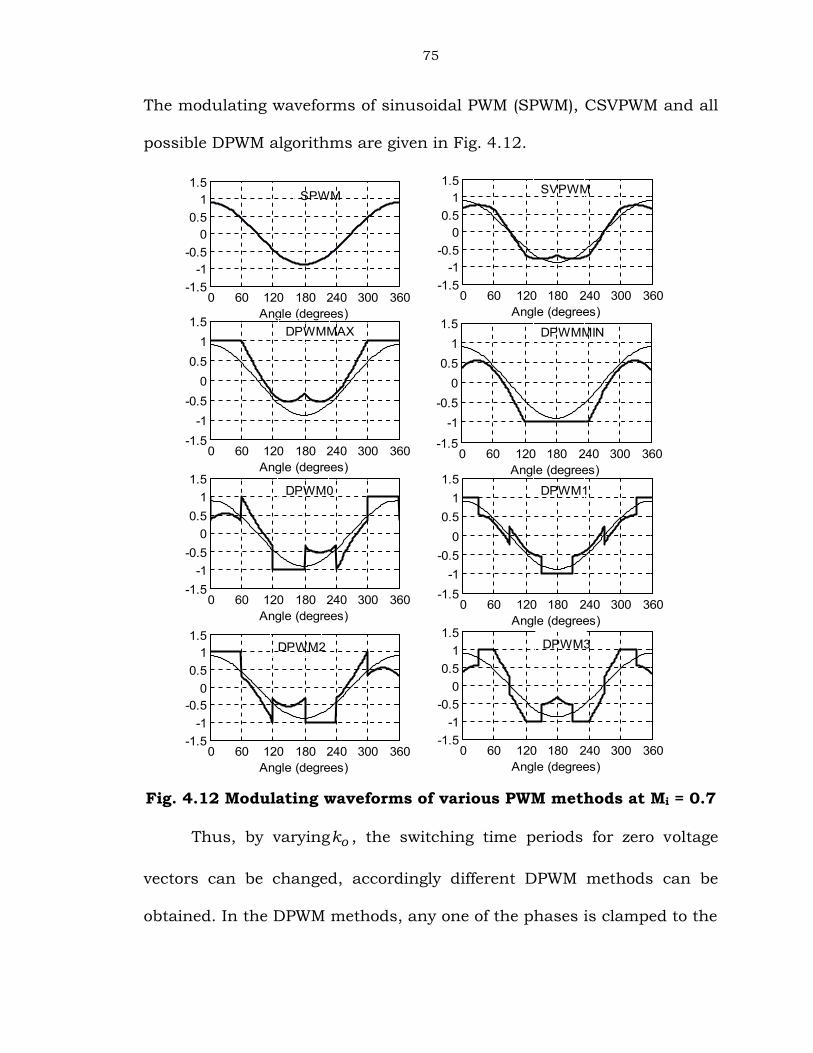
The modulating waveforms of sinusoidal PWM (SPWM), CSVPWM and all
possible DPWM algorithms are given in Fig. 4.12.
Fig. 4.12 Modulating waveforms of various PWM methods at Mi = 0.7
Thus, by varying ok , the switching time periods for zero voltage
vectors can be changed, accordingly different DPWM methods can be
obtained. In the DPWM methods, any one of the phases is clamped to the
76
positive or negative DC bus for utmost a total of 1200 over a fundamental
cycle. Hence, the switching losses of the associated inverter leg are
eliminated. Moreover, within a sampling time period three switchings will
occur in CSVPWM algorithm whereas two switchings in all the above
DPWM algorithms. Hence, the switching frequency of the above DPWM
algorithms is reduced by 33% compared with CSVPWM. Hence a
switching frequency coefficient is introduced as defined in (4.29).
swDPWM
swCSVPWMsw f
fk (4.29)
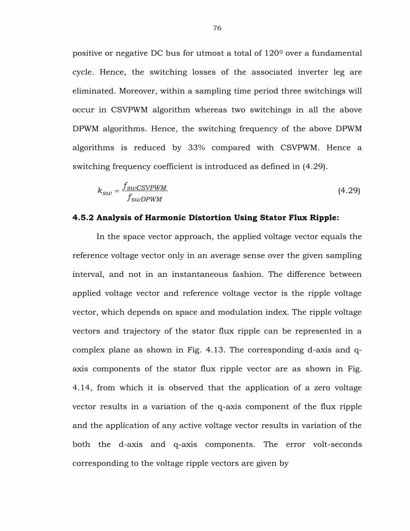
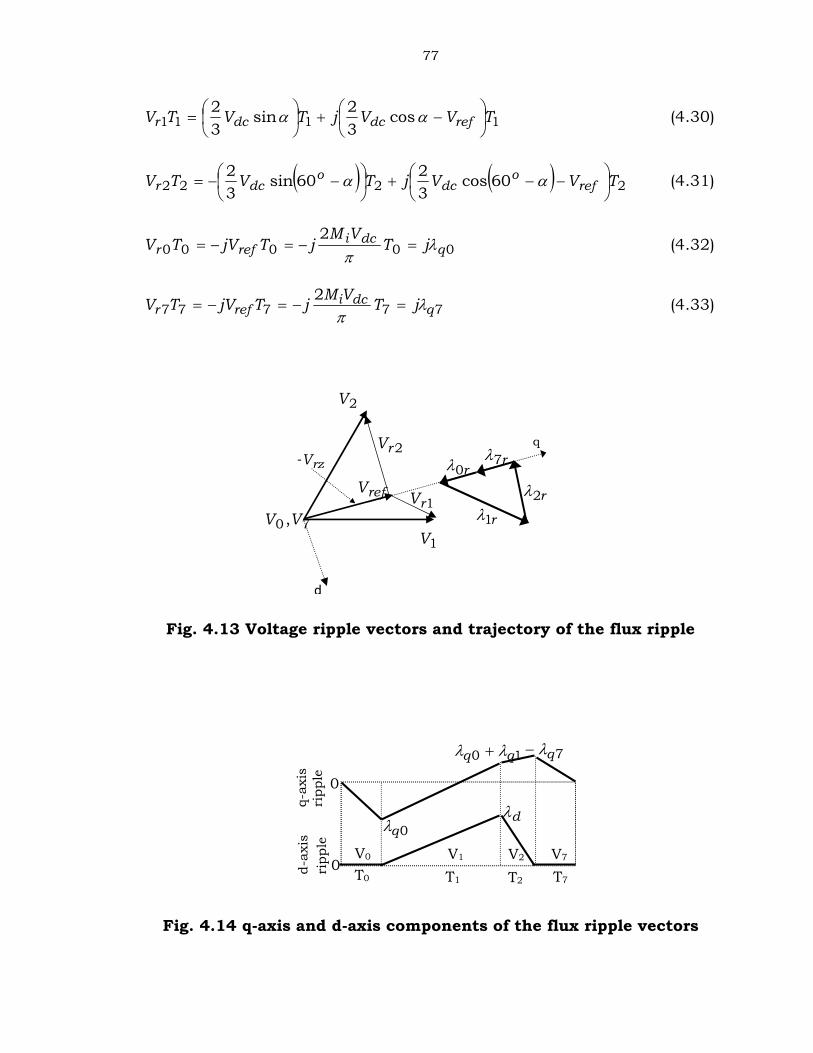
4.5.2 Analysis of Harmonic Distortion Using Stator Flux Ripple:
In the space vector approach, the applied voltage vector equals the
reference voltage vector only in an average sense over the given sampling
interval, and not in an instantaneous fashion. The difference between
applied voltage vector and reference voltage vector is the ripple voltage
vector, which depends on space and modulation index. The ripple voltage
vectors and trajectory of the stator flux ripple can be represented in a
complex plane as shown in Fig. 4.13. The corresponding d-axis and q-
axis components of the stator flux ripple vector are as shown in Fig.
4.14, from which it is observed that the application of a zero voltage
vector results in a variation of the q-axis component of the flux ripple
and the application of any active voltage vector results in variation of the
both the d-axis and q-axis components. The error volt-seconds
corresponding to the voltage ripple vectors are given by
77
1111 cos32sin
32 TVVjTVTV refdcdcr
(4.30)
2222 60cos3260sin
32 TVVjTVTV ref
odc
odcr
(4.31)
000002
qdci
refr jTVM
jTjVTV
(4.32)
777772
qdci
refr jTVMjTjVTV
(4.33)
Fig. 4.13 Voltage ripple vectors and trajectory of the flux ripple
Fig. 4.14 q-axis and d-axis components of the flux ripple vectors
1V
2V
70 ,VV
refV
- rzV2rV
1rVr1
r2
r7r0
q
d
0
0V0
T1
V1 V2 V7
T7
d-ax
isri
pple
q-ax
isri
pple
T0 T2
d
7q10 qq
0q
78
From (4.18) and (4.19)
siTMT
32sin 2 (4.34)
siTMTT
3)5.0(cos 21
(4.35)
siTMTT
3)5.0(60cos 21
(4.36)
and 21 )60sin(32sin
32 TVTV o
dcdc
(4.37)
By substituting (4.34) - (4.37) in (4.30) and (4.31),
1
12121
112
9)5.0(2
33
qd
idc
si
dc
si
dcr
j
TMV
TMTTV
jTTT
MV
TV
(4.38)
2
22121
222
9)5.0(2
33
qd
idc
si
dc
si
dcr
j
TMV
TMTTV
jTTT
MV
TV
(4.39)
The q-axis ripple and d-axis ripple are given in (4.40) and (4.41).
TtT-Tif,t-
TtTif,t
Tt Tif,t
Tt0if,
s7s37
77
2101022
210
10011
10
00
0
T
TTTT
TT
Tt
qqq
(4.40)
79
TtT-Tif0,
TtTif,t-
Tt Tif,t
Tt0if0,
s7s
2101022
10011
0
TTTT
TT
dd
d
d
(4.41)
where, 210310201 T-T-T-tt;T-; TttTtt (4.42)
The mean square stator flux ripple over a sampling interval can be
calculated as
sd
sq
sqqqqqq
sqqqqqq
sq
sT
ds
sT
qs
TTT
TT
TT
TT
TT
dtT
dtT
212727
227107
210
1100
210
20
020
0
2
0
2(rms)
2
)()(
)()(31
11
(4.43)
By using the above formula, the mean square flux ripple can be easily
computed and graphically represented for CSVPWM, DPWMMAX,
DPWMMIN, DPWM0, DPWM1, DPWM2 and DPWM3 methods. The mean
square stator flux ripple characteristics obtained from (4.43) for various
PWM algorithms and for different modulation indices are shown in
Fig.4.15 – Fig.4.20.
80
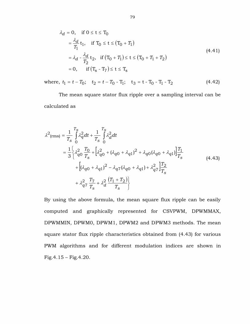
Fig. 4.15 Variation of stator flux ripple over the first sector forMi = 0.4 and ksw=1 (E: CSVPWM, AB: DPWM1, CD: DPWM3, AD:DPWMMAX, DPWM2 and CB: DPWMMIN, DPWM0)
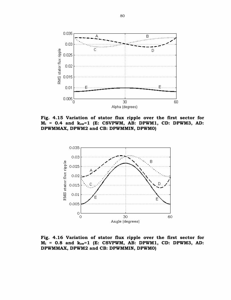
Fig. 4.16 Variation of stator flux ripple over the first sector forMi = 0.8 and ksw=1 (E: CSVPWM, AB: DPWM1, CD: DPWM3, AD:DPWMMAX, DPWM2 and CB: DPWMMIN, DPWM0)
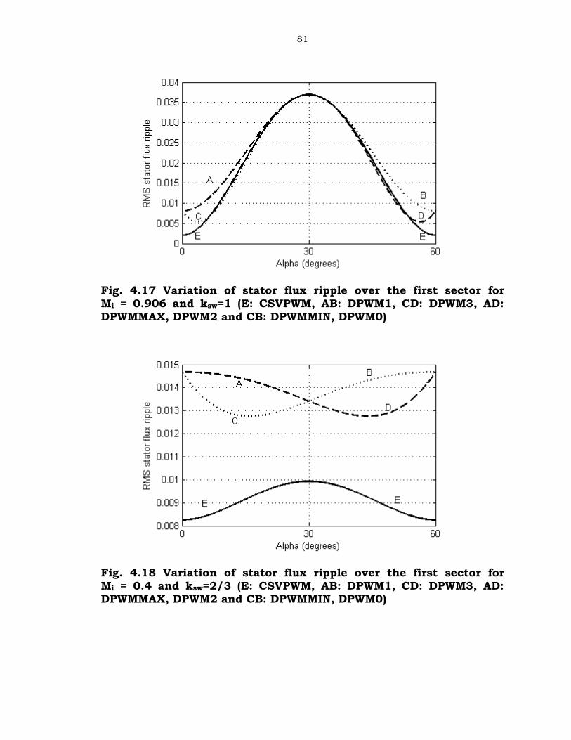
81
Fig. 4.17 Variation of stator flux ripple over the first sector forMi = 0.906 and ksw=1 (E: CSVPWM, AB: DPWM1, CD: DPWM3, AD:DPWMMAX, DPWM2 and CB: DPWMMIN, DPWM0)
Fig. 4.18 Variation of stator flux ripple over the first sector forMi = 0.4 and ksw=2/3 (E: CSVPWM, AB: DPWM1, CD: DPWM3, AD:DPWMMAX, DPWM2 and CB: DPWMMIN, DPWM0)
82
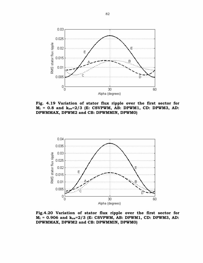
Fig. 4.19 Variation of stator flux ripple over the first sector forMi = 0.8 and ksw=2/3 (E: CSVPWM, AB: DPWM1, CD: DPWM3, AD:DPWMMAX, DPWM2 and CB: DPWMMIN, DPWM0)
Fig.4.20 Variation of stator flux ripple over the first sector forMi = 0.906 and ksw=2/3 (E: CSVPWM, AB: DPWM1, CD: DPWM3, AD:DPWMMAX, DPWM2 and CB: DPWMMIN, DPWM0)
83
From Fig. 4.15 – Fig. 4.20, it can be observed that replacing by
)60( o in the rms stator flux ripple expressions of CSVPWM does not
change its value. It is equivalent to interchanging of T1 and T2 and that of
1q and 2q . It can be seen that such a swapping does not change rms
stator flux ripple expressions of CSVPWM. Thus for a given sampling
time and refV , 0127 sequence produces equal mean square stator flux
ripple at spatial angles and )60( o . However, the rms ripple over a
subcycle is not symmetric about the center of the sector for the other
PWM sequences. Swapping of T1 and T2 and that of 1q and 2q , in the
rms stator flux ripple expression of DPWMMIN lead to the rms stator flux
ripple expression of DPWMMAX. Thus, for a given refV and sT , these can
be shown as follows:
)60()(
)60()(
2)(
2)(
2)(
2)(
oDPWMMAXrmsDPWMINrms
oCSVPWMrmsCSVPWMrms
(4.44)
Also, from Fig. 4.15 – Fig. 4.20, it can be observed that, DPWMMIN
algorithm leads to less rms ripple than DPWMMAX algorithm in the first
half of sector-I. Conversely, DPWMMAX algorithm leads to less rms ripple
than DPWMMIN algorithm in the second half of sector-I as given in
(4.45).
oDPWMMAXrmsDPWMINrms
oDPWMMAXrmsDPWMINrms
6030if)()(
300if)()(
o2)(
2)(
o2)(
2)(
(4.45)
84
The CSVPWM algorithm (0127-7210 sequence) has three switchings per
sampling time period, whereas all the other DPWM algorithms
(DPWMMIN, DPWMMAX, DPWM0, DPWM1, DPWM2 and DPWM3) have
only two switchings per sampling time period. Hence, subcycle duration
32TTs is considered for these DPWM algorithms, while TTs for
CSVPWM algorithm. This ensures comparison of PWM algorithms at the
same average switching frequency, swf . Hence the switching frequency
coefficient is taken as 32swk in this thesis for the simulation studies.
If 32swk , from Fig. 4.15 – Fig. 4.20, it can be observed that at lower
modulation indices, the CSVPWM algorithm gives superior performance
whereas at higher modulation indices the DPWM algorithms give
superior performance. Out of all possible DPWM algorithms, DPWM3
algorithm gives less THD at all modulation indices.
4.5.3 Proposed Hybrid PWM Algorithms:
To minimize the harmonic distortion in the line current, the rms
current ripple or rms stator flux ripple over every sampling time period
should be reduced. The proposed hybrid PWM (HPWM) algorithm employ
the best sequence out of the above possible sequences to minimize the
rms current ripple in every sampling time period. The development of
HPWM technique for reduced current ripple involves determination of
superior performance for every sequence. The zone of superior
performance for a given sequence is the spatial zone within a sector
85
where the given sequence results in less mean square stator flux ripple
than the other sequences considered. By taking the combination of
different sequences various HPWM algorithms can be generated. But, the
proposed HPWM algorithm consists of all the above possible sequences.
In the proposed HPWM algorithm, in every sampling time period the rms
stator flux ripples are compared with each other and the sequence,
which has less rms stator flux ripple is applied to minimize the THD.
Thus, the proposed HPWM algorithm uses the DPWM algorithms in
conjunction with CSVPWM algorithm. Flow chart of the proposed Hybrid
PWM algorithm is shown appendix-III.
4.5.4 Results and Discussion:
To validate the proposed HPWM based vector controlled induction
motor drive, numerical simulation studies have been carried out by using
Matlab/Simulink. The simulation diagrams, parameters and
specifications of induction motor used in this thesis are given in
Appendix – I&III. Various conditions of the drive such as starting, steady
state, step change in load and speed reversal are simulated.
The results for CSVPWM based vector controlled induction motor
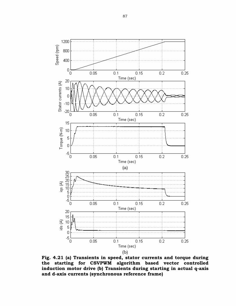
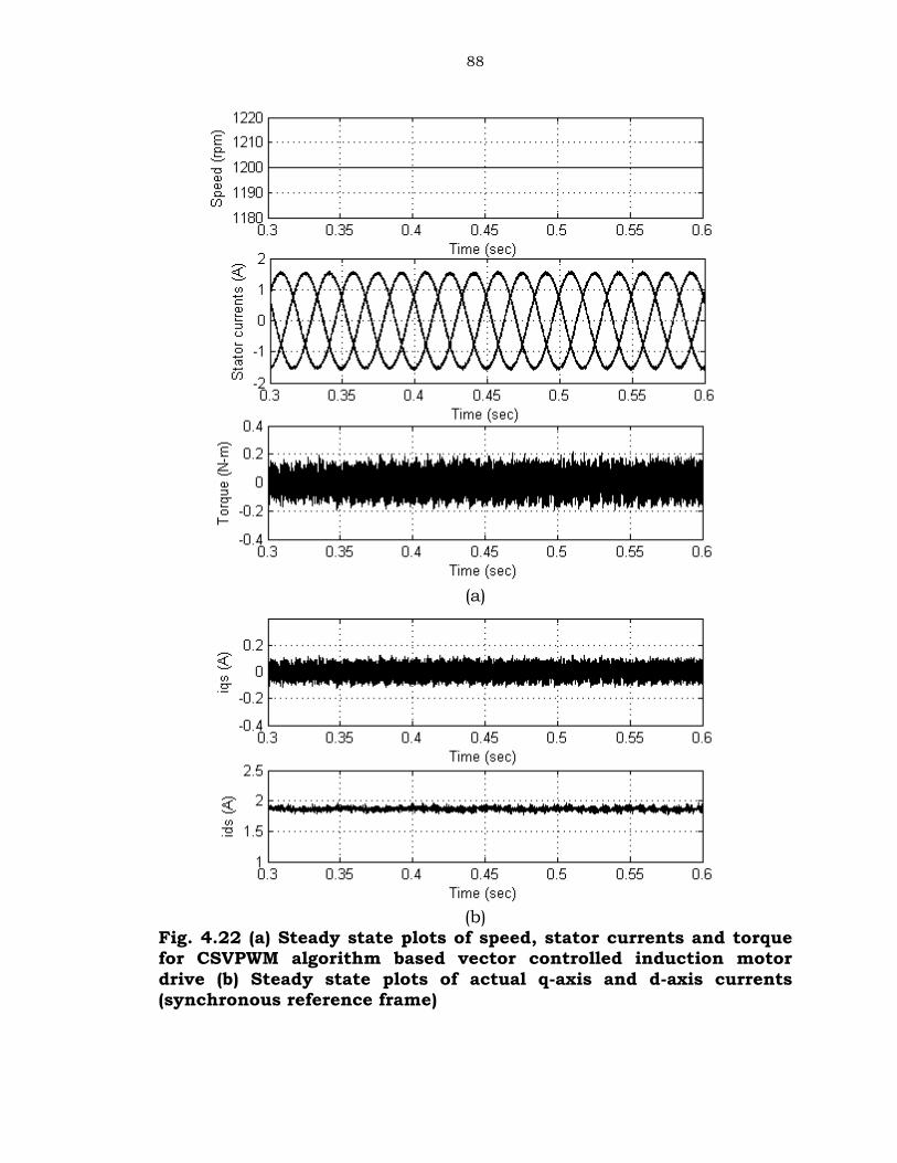
drive are given in Fig. 4.21 – Fig 4.25. Fig.4.21 shows starting transients
of speed, stator currents, torque and d, q axes currents. Fig.4.22
presents the plots under steady state operating conditions. The transient
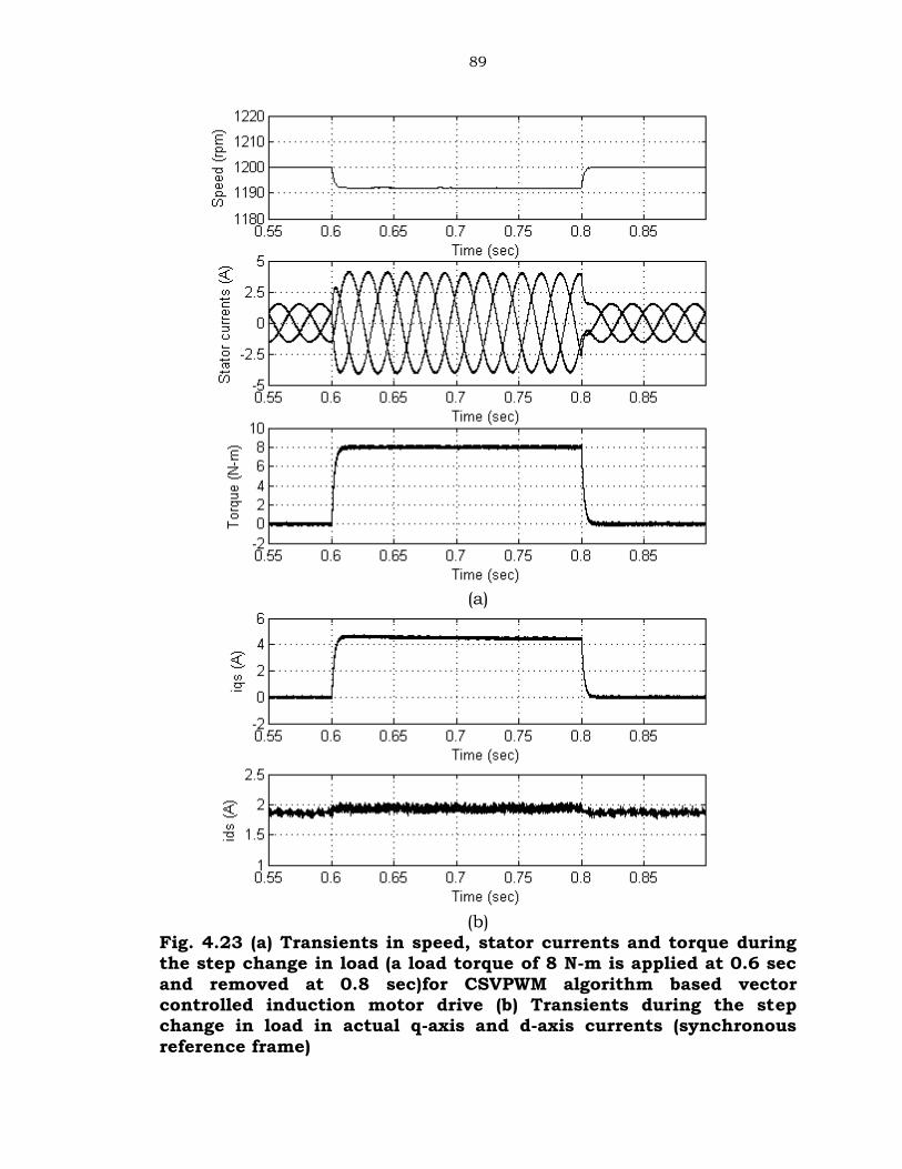
during step change in load (a load torque of 8 N-m is applied at 0.6 sec
and removed at 0.8 sec) is shown in Fig.4.23. The transients of speed,
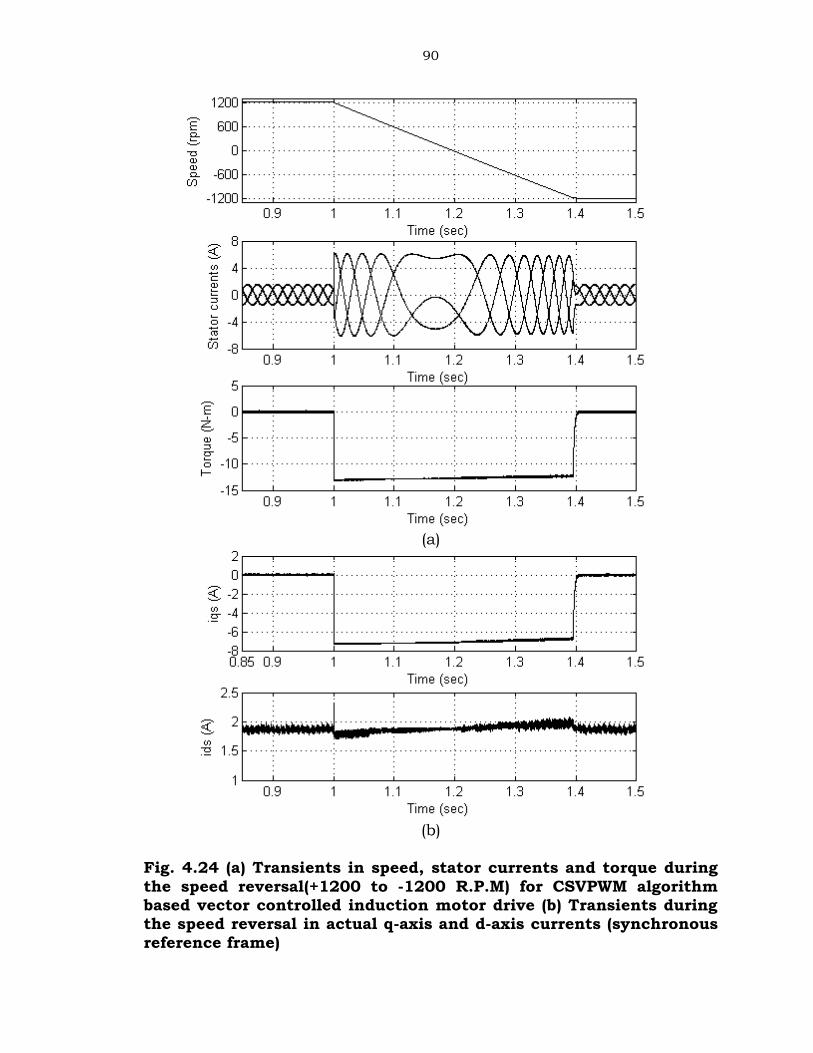
86
stator currents and torque during speed reversal from +1200 to -1200
rpm and -1200 to +1200 rpm are shown in Fig.4.24 and Fig.4.25
respectively. The results for proposed HPWM based vector controlled
induction motor drive are given in Fig. 4.26 – Fig. 4.30. Fig.4.26 shows
starting transients of speed, stator currents, torque and d, q axes
currents. Fig.4.27 presents the plots under steady state operating
conditions. The transients of speed, stator current and torque during
step change in load (a load torque of 8 N-m is applied at 0.6 sec and
removed at 0.8 sec) is shown in Fig.4.28. The transients during speed
reversal from +1200 to -1200 R.P.M. and -1200 to +1200 R.P.M. are
shown in Fig.4.29 and Fig.4.30 respectively. The harmonic spectra of
stator currents for CSVPWM and proposed HPWM based vector control of
induction motor along with their total harmonic distortion (THD) values
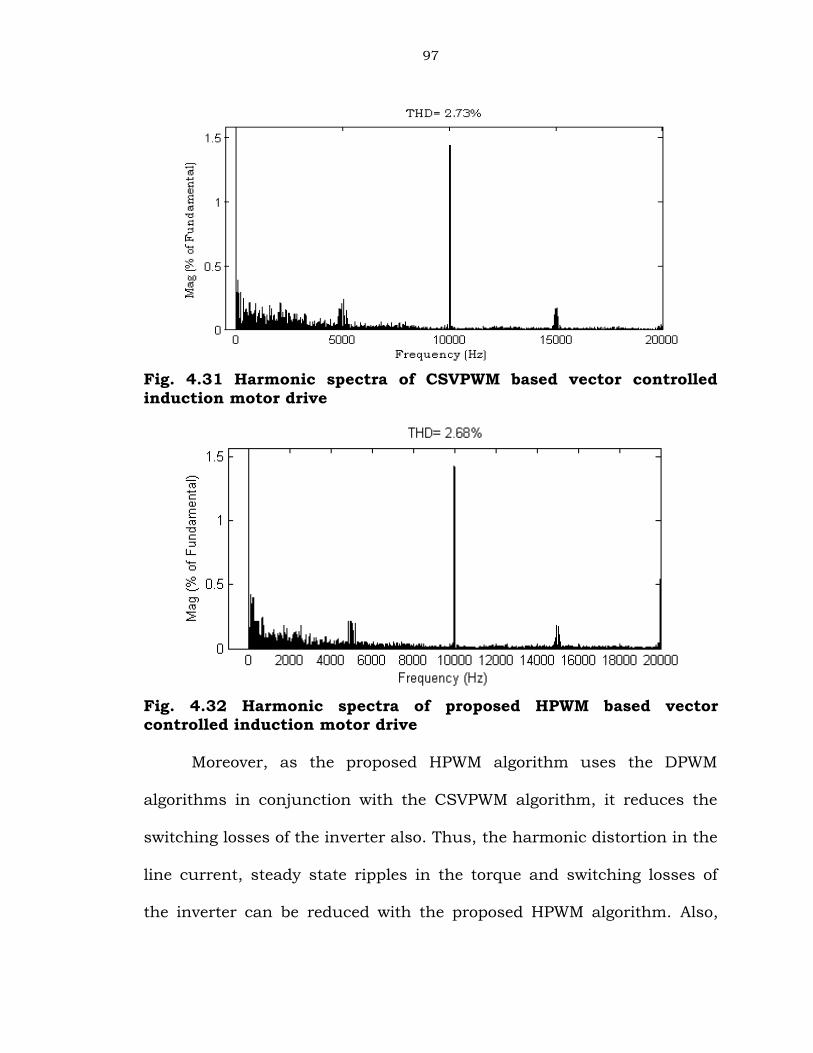
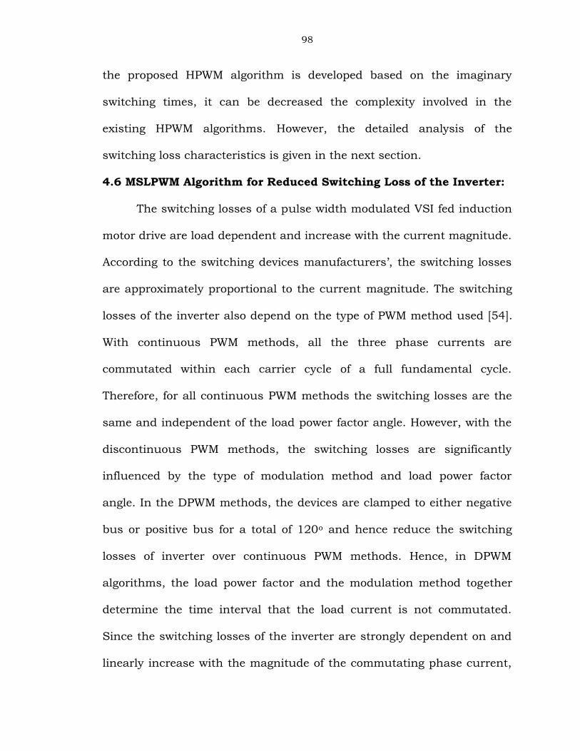
are shown in Fig. 4.31 and Fig. 4.32 respectively.
By observing the steady state results of CSVPWM and HPWM
based vector control of induction motor, it can be observed that the
proposed HPWM algorithm gives less ripples in current and torque. Also,
HPWM gives less THD compared with CSVPWM algorithm. Hence, with
the proposed HPWM algorithm the harmonic distortion in the line
current and hence steady state ripples in the torque and current can be
reduced. From the q-axis and d-axis currents, it can be observed that the
q-axis current is changing according to the torque requirement and d-
axis current is almost constant at all operating conditions.
87
(a)
(b)Fig. 4.21 (a) Transients in speed, stator currents and torque duringthe starting for CSVPWM algorithm based vector controlledinduction motor drive (b) Transients during starting in actual q-axisand d-axis currents (synchronous reference frame)
88
(a)
(b)Fig. 4.22 (a) Steady state plots of speed, stator currents and torquefor CSVPWM algorithm based vector controlled induction motordrive (b) Steady state plots of actual q-axis and d-axis currents(synchronous reference frame)
89
(a)
(b)Fig. 4.23 (a) Transients in speed, stator currents and torque duringthe step change in load (a load torque of 8 N-m is applied at 0.6 secand removed at 0.8 sec)for CSVPWM algorithm based vectorcontrolled induction motor drive (b) Transients during the stepchange in load in actual q-axis and d-axis currents (synchronousreference frame)
90
(a)
(b)
Fig. 4.24 (a) Transients in speed, stator currents and torque duringthe speed reversal(+1200 to -1200 R.P.M) for CSVPWM algorithmbased vector controlled induction motor drive (b) Transients duringthe speed reversal in actual q-axis and d-axis currents (synchronousreference frame)
91
(a)
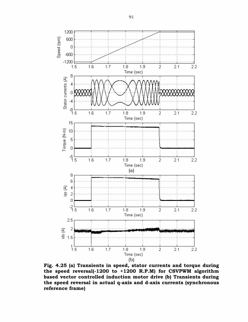
(b)Fig. 4.25 (a) Transients in speed, stator currents and torque duringthe speed reversal(-1200 to +1200 R.P.M) for CSVPWM algorithmbased vector controlled induction motor drive (b) Transients duringthe speed reversal in actual q-axis and d-axis currents (synchronousreference frame)
92
(a)
(b)
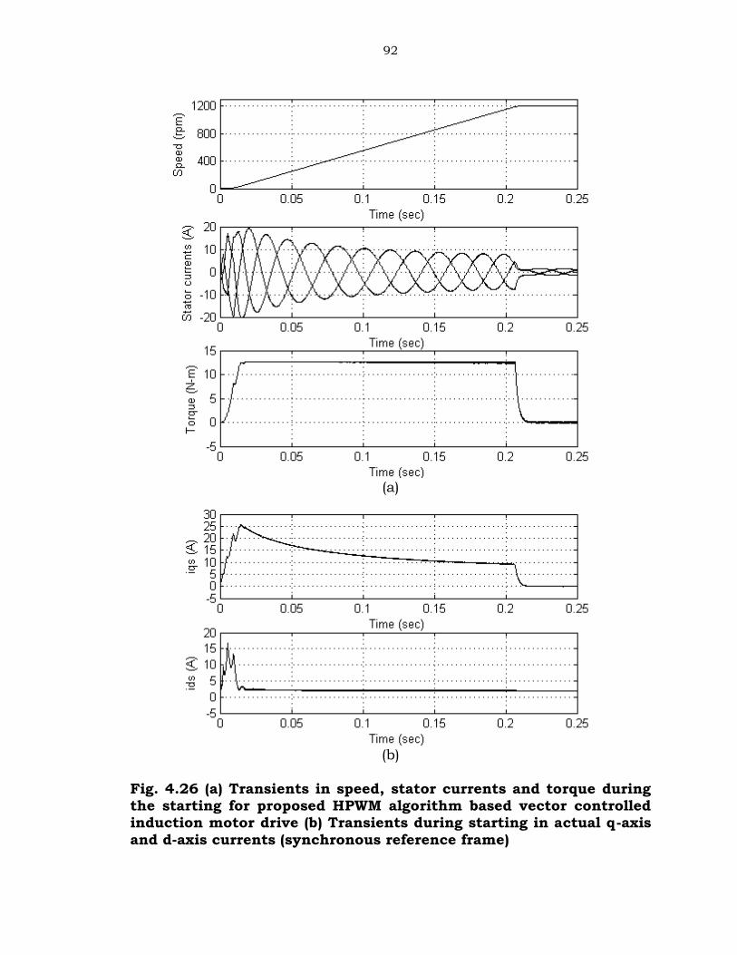
Fig. 4.26 (a) Transients in speed, stator currents and torque duringthe starting for proposed HPWM algorithm based vector controlledinduction motor drive (b) Transients during starting in actual q-axisand d-axis currents (synchronous reference frame)
93
(a)
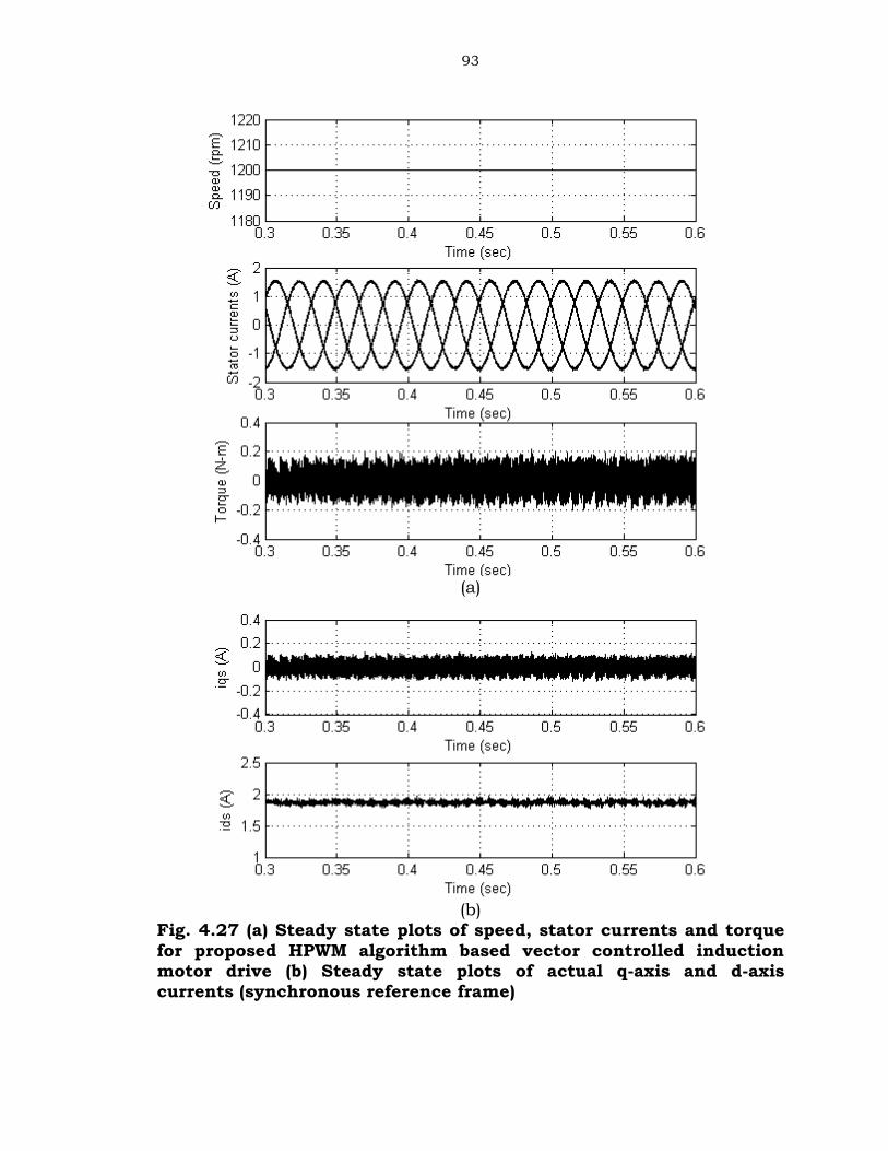
(b)Fig. 4.27 (a) Steady state plots of speed, stator currents and torquefor proposed HPWM algorithm based vector controlled inductionmotor drive (b) Steady state plots of actual q-axis and d-axiscurrents (synchronous reference frame)

94
(a)
(b)Fig. 4.28 (a) Transients in speed, stator currents and torque duringthe step change in load(a load torque of 8 N-m is applied at 0.6 secand removed at 0.8 sec) for proposed HPWM algorithm based vectorcontrolled induction motor drive (b) Transients during the stepchange in load in actual q-axis and d-axis currents (synchronousreference frame)
95
(a)
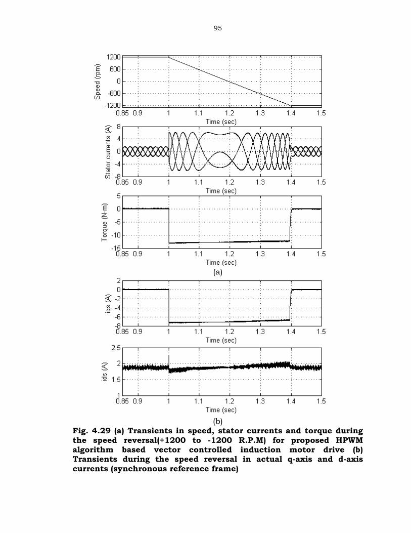
(b)Fig. 4.29 (a) Transients in speed, stator currents and torque duringthe speed reversal(+1200 to -1200 R.P.M) for proposed HPWMalgorithm based vector controlled induction motor drive (b)Transients during the speed reversal in actual q-axis and d-axiscurrents (synchronous reference frame)
96
(a)
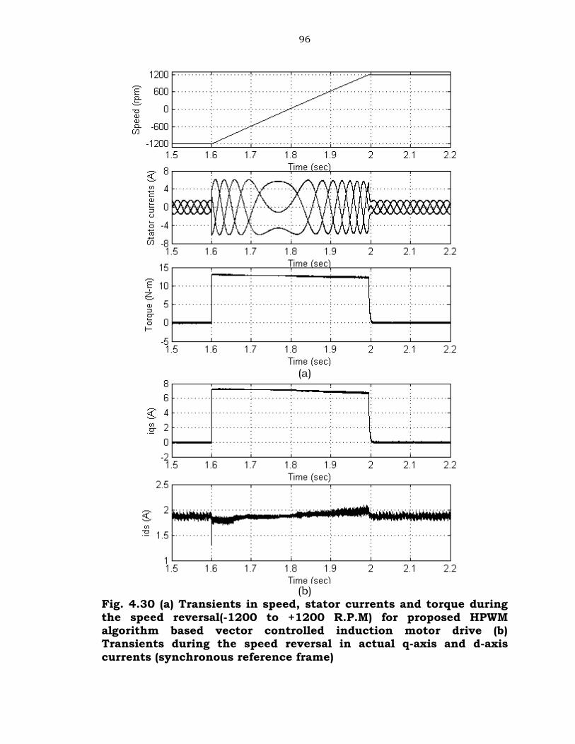
(b)Fig. 4.30 (a) Transients in speed, stator currents and torque duringthe speed reversal(-1200 to +1200 R.P.M) for proposed HPWMalgorithm based vector controlled induction motor drive (b)Transients during the speed reversal in actual q-axis and d-axiscurrents (synchronous reference frame)
97
Fig. 4.31 Harmonic spectra of CSVPWM based vector controlledinduction motor drive
Fig. 4.32 Harmonic spectra of proposed HPWM based vectorcontrolled induction motor drive
Moreover, as the proposed HPWM algorithm uses the DPWM
algorithms in conjunction with the CSVPWM algorithm, it reduces the
switching losses of the inverter also. Thus, the harmonic distortion in the
line current, steady state ripples in the torque and switching losses of
the inverter can be reduced with the proposed HPWM algorithm. Also,
98
the proposed HPWM algorithm is developed based on the imaginary
switching times, it can be decreased the complexity involved in the
existing HPWM algorithms. However, the detailed analysis of the
switching loss characteristics is given in the next section.
4.6 MSLPWM Algorithm for Reduced Switching Loss of the Inverter:
The switching losses of a pulse width modulated VSI fed induction
motor drive are load dependent and increase with the current magnitude.
According to the switching devices manufacturers’, the switching losses
are approximately proportional to the current magnitude. The switching
losses of the inverter also depend on the type of PWM method used [54].
With continuous PWM methods, all the three phase currents are
commutated within each carrier cycle of a full fundamental cycle.
Therefore, for all continuous PWM methods the switching losses are the
same and independent of the load power factor angle. However, with the
discontinuous PWM methods, the switching losses are significantly
influenced by the type of modulation method and load power factor
angle. In the DPWM methods, the devices are clamped to either negative
bus or positive bus for a total of 120o and hence reduce the switching
losses of inverter over continuous PWM methods. Hence, in DPWM
algorithms, the load power factor and the modulation method together
determine the time interval that the load current is not commutated.
Since the switching losses of the inverter are strongly dependent on and
linearly increase with the magnitude of the commutating phase current,
99
selecting a DPWM method with reduced switching losses can
significantly contribute to the performance of an induction motor drive.
Therefore, it is necessary to derive the switching loss characteristics to
compare the switching losses of various DPWM algorithms. This section
presents a comparison of inverter switching losses due to conventional
SVPWM and existing DPWM methods.
The switching loss in an IGBT depends mainly on the dc link
voltage (Vdc), instantaneous line current and turn-on and turn-off times.
However, the Vdc and times are assumed to be constant for different
instantaneous line currents. Hence, to study the switching losses of the
inverter, it is sufficient to consider the product of instantaneous line
current magnitude of a particular phase and the number of switchings
per sampling time period in that phase ( an ), corresponding to the PWM
sequence considered. This product is referred to as the switching loss
factor (SLF). Since the three phases are symmetric, it is enough to
analyze one phase only. The switching losses of a PWM-VSI induction
motor drive can be modeled analytically by assuming linear current turn-
on and turn-off characteristics with respect to time for the inverter
switching devices and considering only fundamental component of the
load current. Let the phase current be
)sin(max tIia (4.46)
where ai is the instantaneous fundamental phase current, maxI is the
maximum value of the fundamental phase current and is the line side
100
power factor angle. The average switching energy loss per subcycle
)( subE in an inverter leg is as given by [76]
)()sin(1)()sin(1)(
00 max
max tdtntdI
tInavgE a
asub
(4.47)
To obtain the measure of the inverter switching losses, the average
switching energy loss per subcycle must be multiplied by the number of
subcycles per second, i.e., the sampling frequency ( sf ). The sampling
frequency of the CSVPWM is two times the switching frequency ( swf ),
while it is three times the switching frequency ( swf ) for the above DPWM
methods. The average switching energy loss over a fundamental cycle for
CSVPWM equals (2/ ). The normalized switching loss due to given PWM
algorithm can be obtained as given in (4.48) [76].
sw
ssubsw f
favgEP
2*
2)(
(4.48)
From (4.48), the normalized switching loss due to existing DPWM
methods can be obtained and given in (4.49).
)(4
3 avgEP subsw
(4.49)
By observing the DPWM0, DPWM1 and DPWM2 modulating
waveforms, it can be given that there is a 30o phase-angle ( ) distance
between their dc-link clamped 60o segments. Hence, a new PWM
algorithm can be introduced as generalized DPWM (GDPWM) algorithm
which covers the DPWM0, DPWM1 and DPWM2 algorithms. The and
101
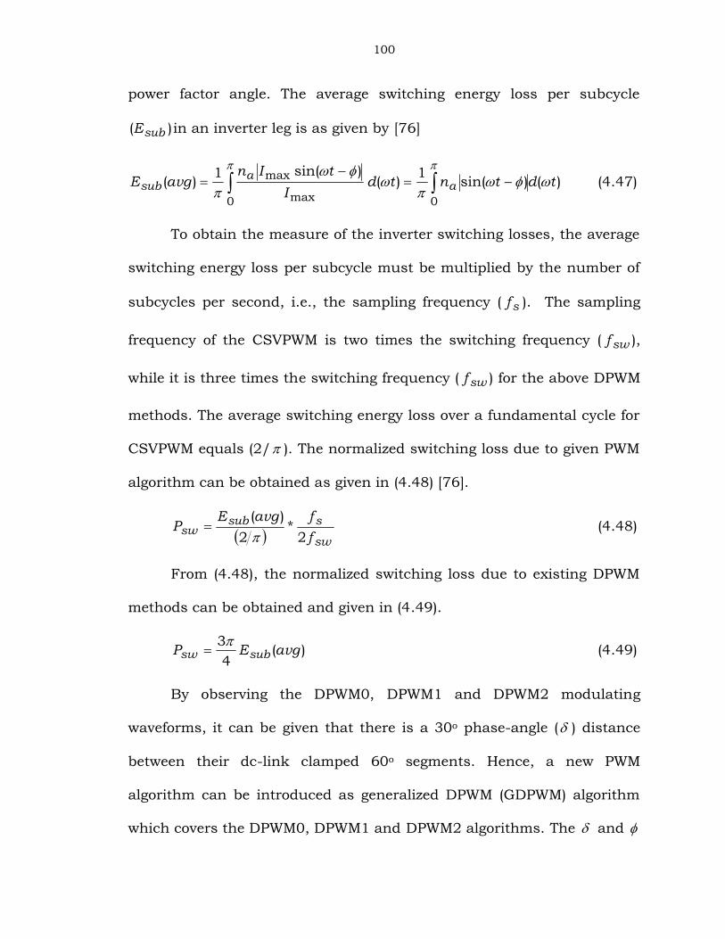
dependent switching phase current and normalized switching energy loss
per subcycle waveforms of GDPWM algorithm is shown in Fig.4.33.
Fig. 4.33 The average switching loss of GDPWM
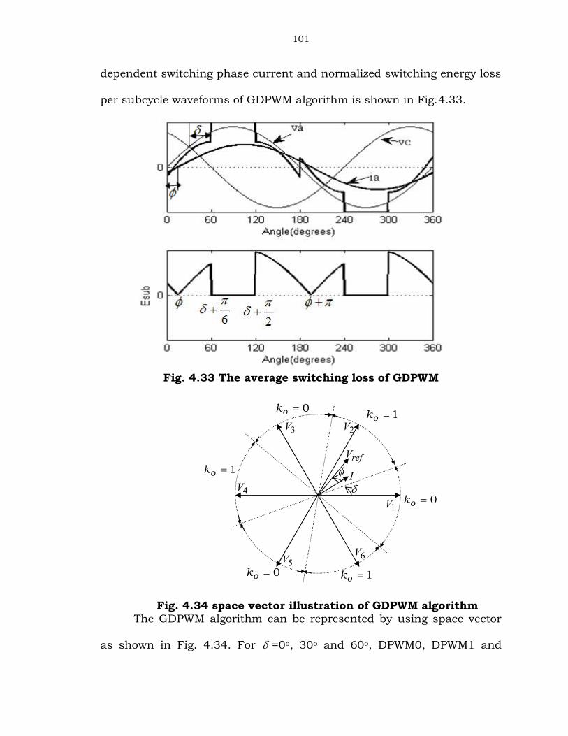
Fig. 4.34 space vector illustration of GDPWM algorithmThe GDPWM algorithm can be represented by using space vector
as shown in Fig. 4.34. For =0o, 30o and 60o, DPWM0, DPWM1 and
refV
I
0ok
1ok
0ok
0ok
1ok
1ok
1V
3V 2V
4V
5V 6V
102
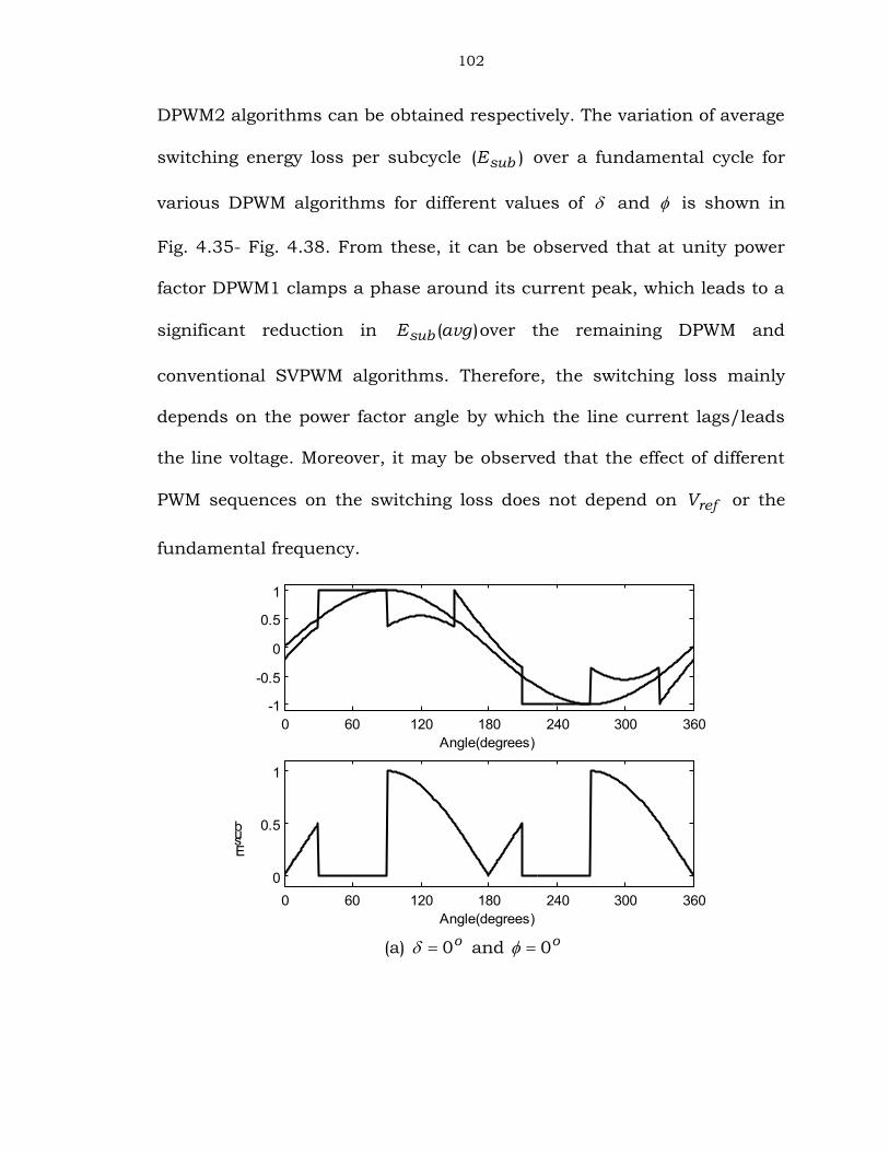
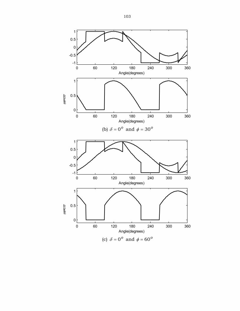
DPWM2 algorithms can be obtained respectively. The variation of average
switching energy loss per subcycle )( subE over a fundamental cycle for
various DPWM algorithms for different values of and is shown in
Fig. 4.35- Fig. 4.38. From these, it can be observed that at unity power
factor DPWM1 clamps a phase around its current peak, which leads to a
significant reduction in )(avgEsub over the remaining DPWM and
conventional SVPWM algorithms. Therefore, the switching loss mainly
depends on the power factor angle by which the line current lags/leads
the line voltage. Moreover, it may be observed that the effect of different
PWM sequences on the switching loss does not depend on refV or the
fundamental frequency.
0 60 120 180 240 300 360-1
-0.5
0
0.5
1
Angle(degrees)
0 60 120 180 240 300 3600
0.5
1
Angle(degrees)
Esub
(a) o0 and o0
103
0 60 120 180 240 300 360-1
-0.5
0
0.5
1
Angle(degrees)
0 60 120 180 240 300 3600
0.5
1
Angle(degrees)
Esub
(b) o0 and o30
0 60 120 180 240 300 360-1
-0.5
0
0.5
1
Angle(degrees)
0 60 120 180 240 300 3600
0.5
1
Angle(degrees)
Esub
(c) o0 and o60
104
0 60 120 180 240 300 360-1
-0.5
0
0.5
1
Angle(degrees)
0 60 120 180 240 300 3600
0.5
1
Angle(degrees)
Esub
(d) o0 and o90
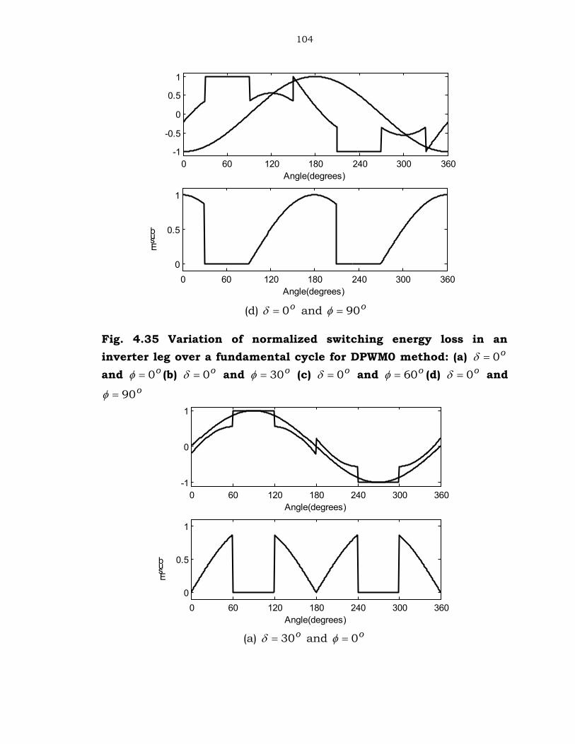
Fig. 4.35 Variation of normalized switching energy loss in aninverter leg over a fundamental cycle for DPWM0 method: (a) o0and o0 (b) o0 and o30 (c) o0 and o60 (d) o0 and
o90
0 60 120 180 240 300 360-1
0
1
Angle(degrees)
0 60 120 180 240 300 3600
0.5
1
Angle(degrees)
Esub
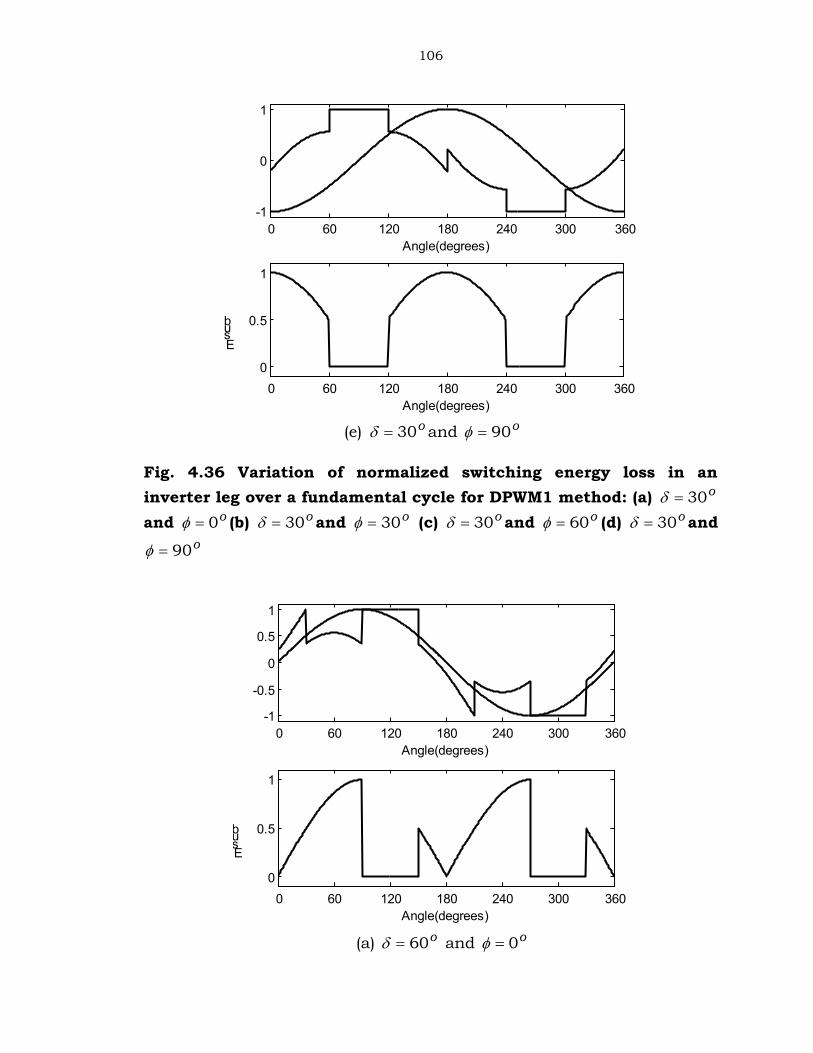
(a) o30 and o0
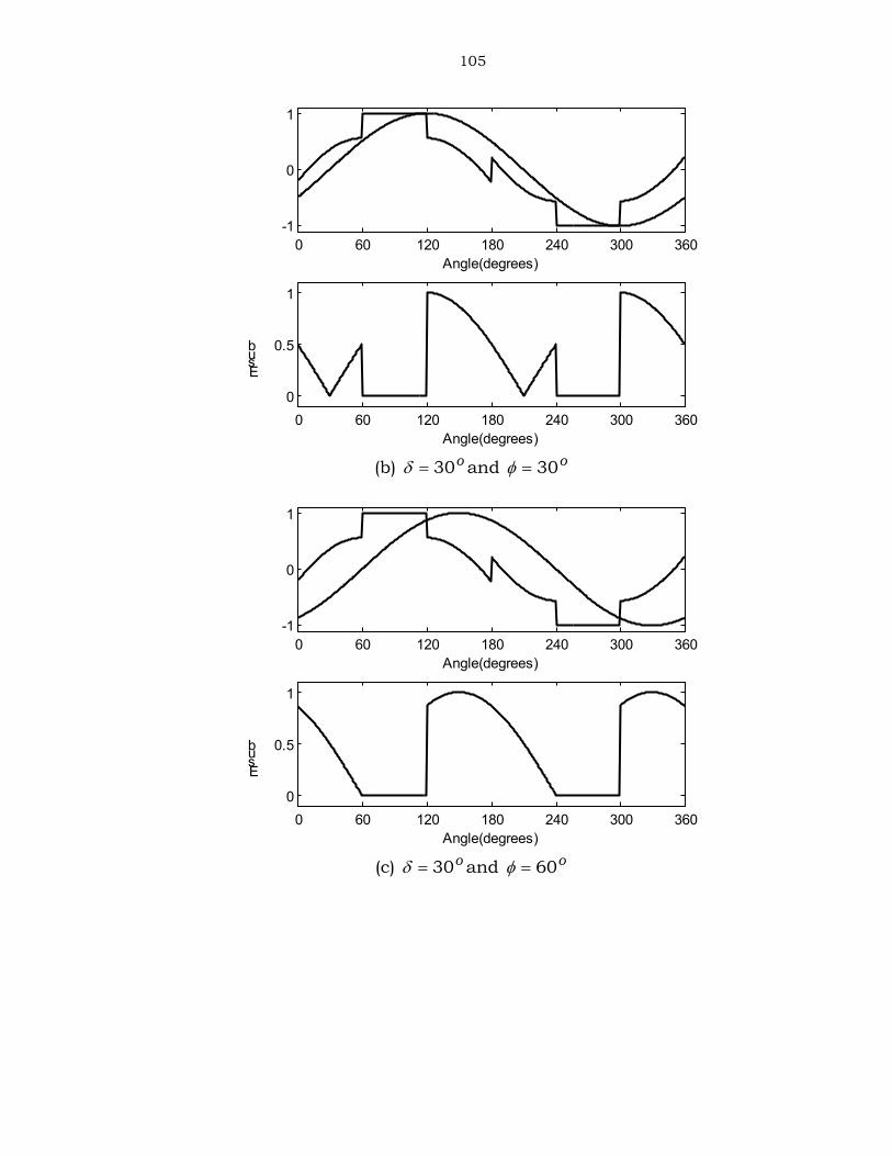
105
0 60 120 180 240 300 360-1
0
1
Angle(degrees)
0 60 120 180 240 300 3600
0.5
1
Angle(degrees)
Esub
(b) o30 and o30
0 60 120 180 240 300 360-1
0
1
Angle(degrees)
0 60 120 180 240 300 3600
0.5
1
Angle(degrees)
Esub
(c) o30 and o60
106
0 60 120 180 240 300 360-1
0
1
Angle(degrees)
0 60 120 180 240 300 3600
0.5
1
Angle(degrees)
Esub
(e) o30 and o90
Fig. 4.36 Variation of normalized switching energy loss in aninverter leg over a fundamental cycle for DPWM1 method: (a) o30and o0 (b) o30 and o30 (c) o30 and o60 (d) o30 and
o90
0 60 120 180 240 300 360-1
-0.5
0
0.5
1
Angle(degrees)
0 60 120 180 240 300 3600
0.5
1
Angle(degrees)
Esub
(a) o60 and o0
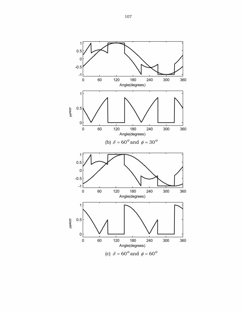
107
0 60 120 180 240 300 360-1
-0.5
0
0.5
1
Angle(degrees)
0 60 120 180 240 300 3600
0.5
1
Angle(degrees)
Esub
(b) o60 and o30
0 60 120 180 240 300 360-1
-0.5
0
0.5
1
Angle(degrees)
0 60 120 180 240 300 3600
0.5
1
Angle(degrees)
Esub
(c) o60 and o60
108
0 60 120 180 240 300 360-1
-0.5
0
0.5
1
Angle(degrees)
0 60 120 180 240 300 3600
0.5
1
Angle(degrees)
Esub
(d) o60 and o90
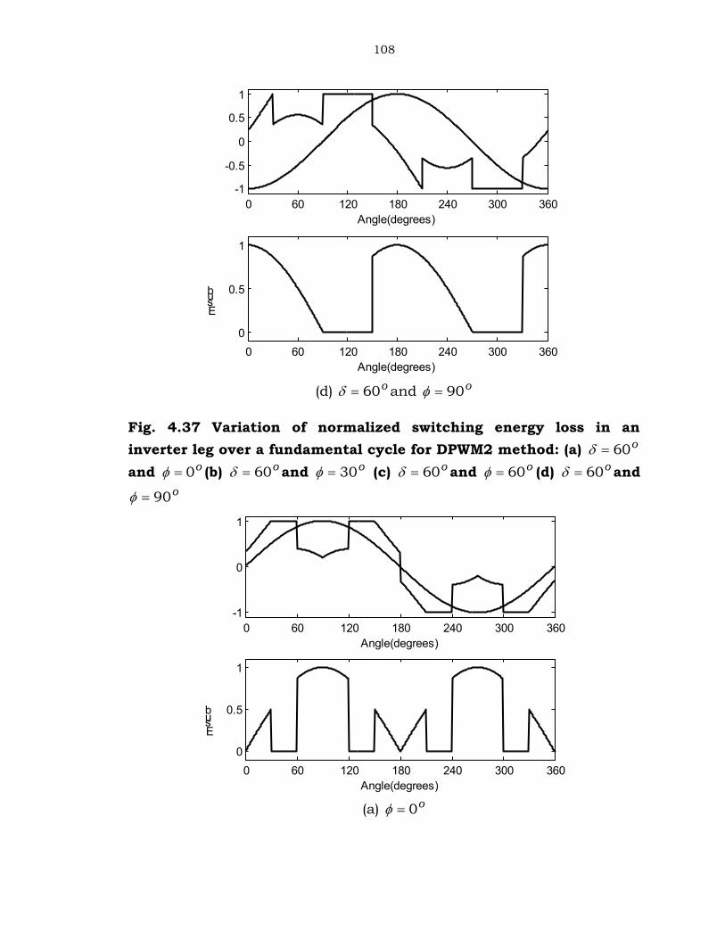
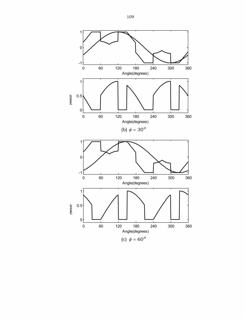
Fig. 4.37 Variation of normalized switching energy loss in aninverter leg over a fundamental cycle for DPWM2 method: (a) o60and o0 (b) o60 and o30 (c) o60 and o60 (d) o60 and
o90
0 60 120 180 240 300 360-1
0
1
Angle(degrees)
0 60 120 180 240 300 3600
0.5
1
Angle(degrees)
Esub
(a) o0
109
0 60 120 180 240 300 360-1
0
1
Angle(degrees)
0 60 120 180 240 300 3600
0.5
1
Angle(degrees)
Esub
(b) o30
0 60 120 180 240 300 360-1
0
1
Angle(degrees)
0 60 120 180 240 300 3600
0.5
1
Angle(degrees)
Esub
(c) o60
110
0 60 120 180 240 300 360-1
0
1
Angle(degrees)
0 60 120 180 240 300 3600
0.5
1
Angle(degrees)
Esub
(d) o90
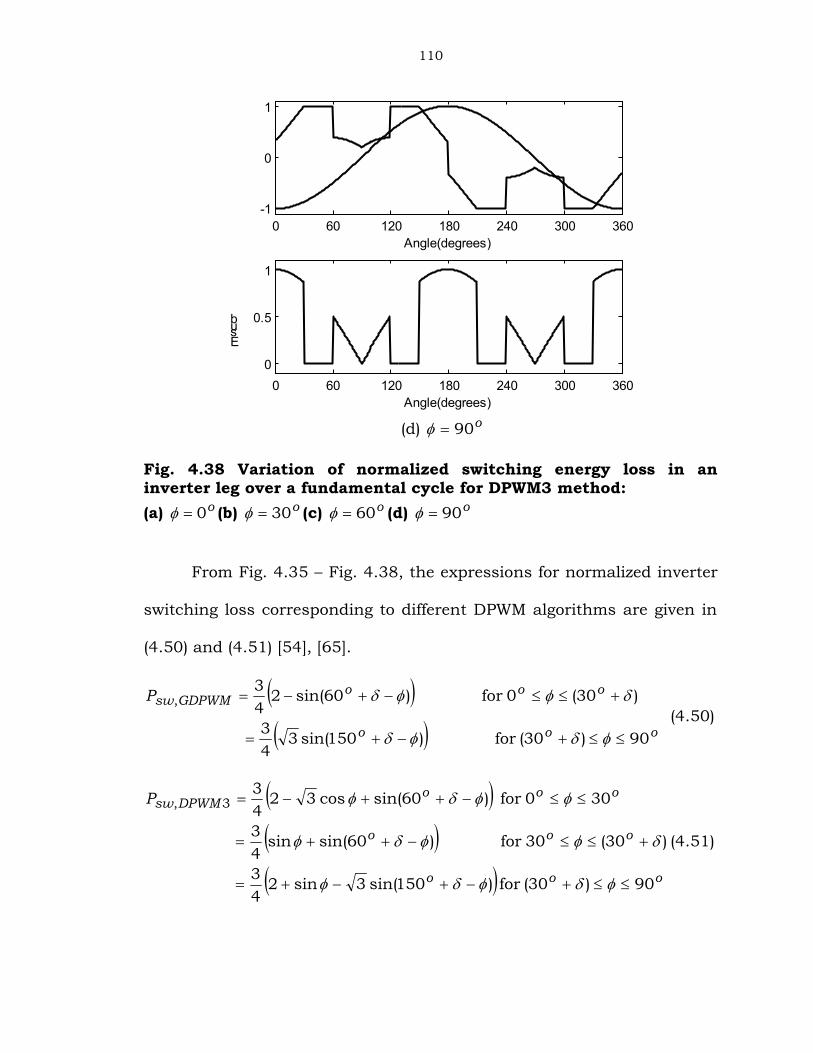
Fig. 4.38 Variation of normalized switching energy loss in aninverter leg over a fundamental cycle for DPWM3 method:(a) o0 (b) o30 (c) o60 (d) o90
From Fig. 4.35 – Fig. 4.38, the expressions for normalized inverter
switching loss corresponding to different DPWM algorithms are given in
(4.50) and (4.51) [54], [65].
ooo
oooGDPWMswP
90)30(for)150sin(343
)30(0for)60sin(243
,
(4.50)
ooo
ooo
oooDPWMswP
90)30(for)150sin(3sin243
)30(30for)60sin(sin43
300for)60sin(cos3243
3,
(4.51)
111
The normalized switching loss expressions for DPWM0, DPWM1
and DPWM2 can be obtained from (4.50) by substituting =0o, 30o and
60o respectively. From (4.50) and (4.51), it can be observed that the
normalized switching loss expressions of existing DPWM methods are the
function of both and . The variation of normalized switching loss of
different DPWM algorithms with power factor angle (both at lagging and
leading) is shown in Fig. 4.39.
-90 -75 -60 -45 -30 -15 0 15 30 45 60 75 900.7
0.8
0.9
1
1.1
1.2
1.3
1.4
Power factor angle (degrees)
Psw
A
B
D
C
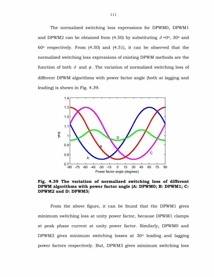
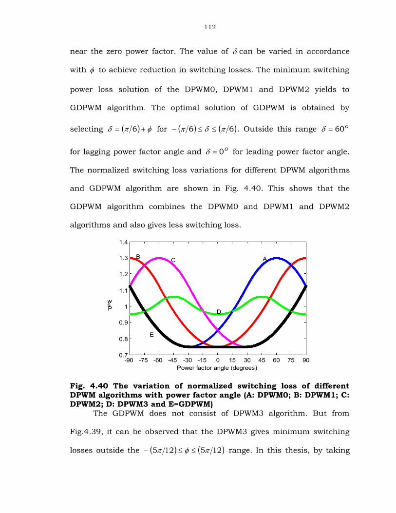
Fig. 4.39 The variation of normalized switching loss of differentDPWM algorithms with power factor angle (A: DPWM0; B: DPWM1; C:DPWM2 and D: DPWM3)
From the above figure, it can be found that the DPWM1 gives
minimum switching loss at unity power factor, because DPWM1 clamps
at peak phase current at unity power factor. Similarly, DPWM0 and
DPWM2 gives minimum switching losses at 30o leading and lagging
power factors respectively. But, DPWM3 gives minimum switching loss
112
near the zero power factor. The value of can be varied in accordance
with to achieve reduction in switching losses. The minimum switching
power loss solution of the DPWM0, DPWM1 and DPWM2 yields to
GDPWM algorithm. The optimal solution of GDPWM is obtained by
selecting 6 for 66 . Outside this range o60
for lagging power factor angle and o0 for leading power factor angle.
The normalized switching loss variations for different DPWM algorithms
and GDPWM algorithm are shown in Fig. 4.40. This shows that the
GDPWM algorithm combines the DPWM0 and DPWM1 and DPWM2
algorithms and also gives less switching loss.
-90 -75 -60 -45 -30 -15 0 15 30 45 60 75 900.7
0.8
0.9
1
1.1
1.2
1.3
1.4
Power factor angle (degrees)
Psw
B C A
D
E
Fig. 4.40 The variation of normalized switching loss of differentDPWM algorithms with power factor angle (A: DPWM0; B: DPWM1; C:DPWM2; D: DPWM3 and E=GDPWM)
The GDPWM does not consist of DPWM3 algorithm. But from
Fig.4.39, it can be observed that the DPWM3 gives minimum switching
losses outside the 125125 range. In this thesis, by taking
113
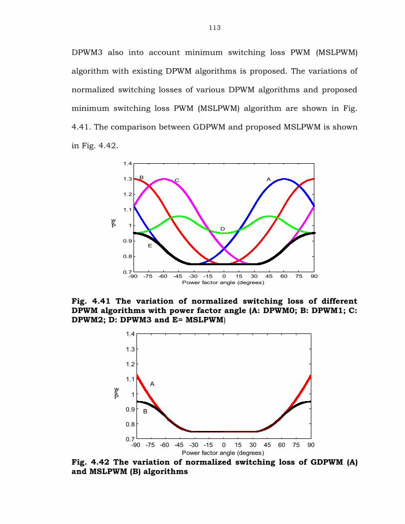
DPWM3 also into account minimum switching loss PWM (MSLPWM)
algorithm with existing DPWM algorithms is proposed. The variations of
normalized switching losses of various DPWM algorithms and proposed
minimum switching loss PWM (MSLPWM) algorithm are shown in Fig.
4.41. The comparison between GDPWM and proposed MSLPWM is shown
in Fig. 4.42.
-90 -75 -60 -45 -30 -15 0 15 30 45 60 75 900.7
0.8
0.9
1
1.1
1.2
1.3
1.4
Power factor angle (degrees)
Psw
B C A
D
E
Fig. 4.41 The variation of normalized switching loss of differentDPWM algorithms with power factor angle (A: DPWM0; B: DPWM1; C:DPWM2; D: DPWM3 and E= MSLPWM)
-90 -75 -60 -45 -30 -15 0 15 30 45 60 75 900.7
0.8
0.9
1
1.1
1.2
1.3
1.4
Power factor angle (degrees)
Psw
A
B
Fig. 4.42 The variation of normalized switching loss of GDPWM (A)and MSLPWM (B) algorithms
114
To minimize the normalized switching losses of inverter with
existing DPWM algorithm, the type of clamping and the value of must
be as shown in Table 4.2.
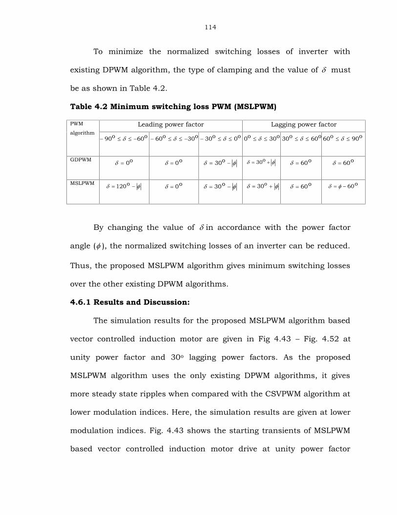
Table 4.2 Minimum switching loss PWM (MSLPWM)
PWM
algorithmLeading power factor Lagging power factor
o60o90 o30o60 o0o30 o30o0 o60o30 o90o60
GDPWM o0 o0 o30 o30 o60 o60
MSLPWM o120 o0 o30 o30 o60 o60
By changing the value of in accordance with the power factor
angle ( ), the normalized switching losses of an inverter can be reduced.
Thus, the proposed MSLPWM algorithm gives minimum switching losses
over the other existing DPWM algorithms.
4.6.1 Results and Discussion:
The simulation results for the proposed MSLPWM algorithm based
vector controlled induction motor are given in Fig 4.43 – Fig. 4.52 at
unity power factor and 30o lagging power factors. As the proposed
MSLPWM algorithm uses the only existing DPWM algorithms, it gives
more steady state ripples when compared with the CSVPWM algorithm at
lower modulation indices. Here, the simulation results are given at lower
modulation indices. Fig. 4.43 shows the starting transients of MSLPWM
based vector controlled induction motor drive at unity power factor
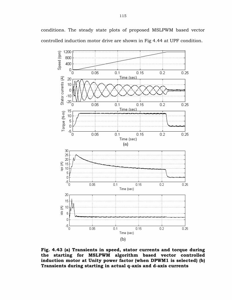
115
conditions. The steady state plots of proposed MSLPWM based vector
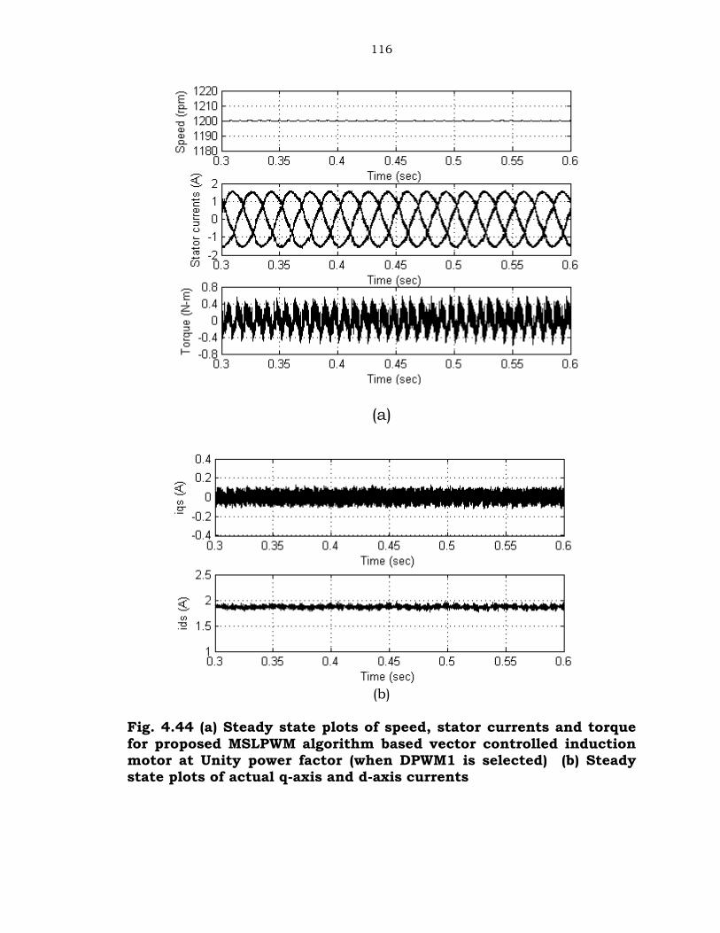
controlled induction motor drive are shown in Fig 4.44 at UPF condition.
(a)
(b)
Fig. 4.43 (a) Transients in speed, stator currents and torque duringthe starting for MSLPWM algorithm based vector controlledinduction motor at Unity power factor (when DPWM1 is selected) (b)Transients during starting in actual q-axis and d-axis currents
116
(a)
(b)
Fig. 4.44 (a) Steady state plots of speed, stator currents and torquefor proposed MSLPWM algorithm based vector controlled inductionmotor at Unity power factor (when DPWM1 is selected) (b) Steadystate plots of actual q-axis and d-axis currents
117
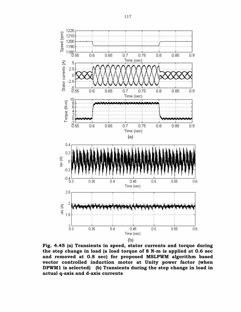
(a)
(b)Fig. 4.45 (a) Transients in speed, stator currents and torque duringthe step change in load (a load torque of 8 N-m is applied at 0.6 secand removed at 0.8 sec) for proposed MSLPWM algorithm basedvector controlled induction motor at Unity power factor (whenDPWM1 is selected) (b) Transients during the step change in load inactual q-axis and d-axis currents
118
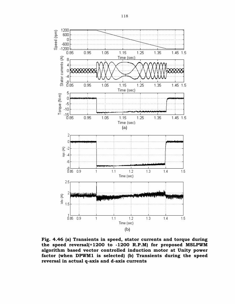
(a)
(b)
Fig. 4.46 (a) Transients in speed, stator currents and torque duringthe speed reversal(+1200 to -1200 R.P.M) for proposed MSLPWMalgorithm based vector controlled induction motor at Unity powerfactor (when DPWM1 is selected) (b) Transients during the speedreversal in actual q-axis and d-axis currents
119
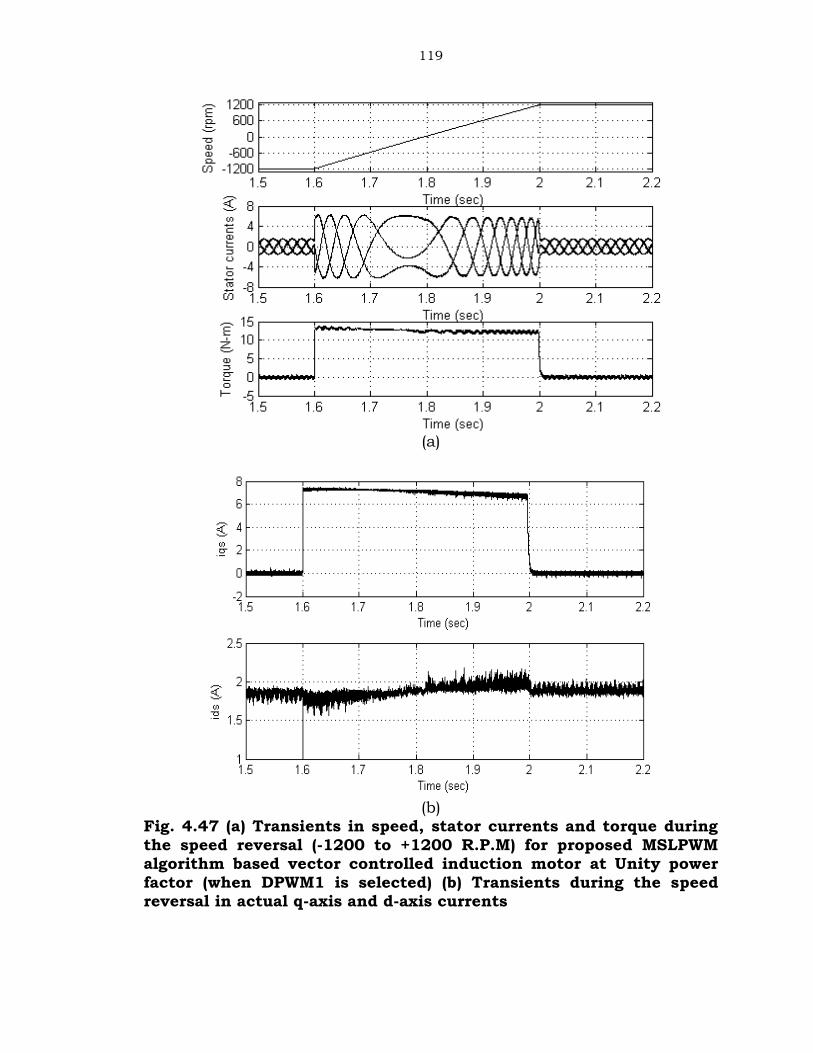
(a)
(b)Fig. 4.47 (a) Transients in speed, stator currents and torque duringthe speed reversal (-1200 to +1200 R.P.M) for proposed MSLPWMalgorithm based vector controlled induction motor at Unity powerfactor (when DPWM1 is selected) (b) Transients during the speedreversal in actual q-axis and d-axis currents
120
(a)
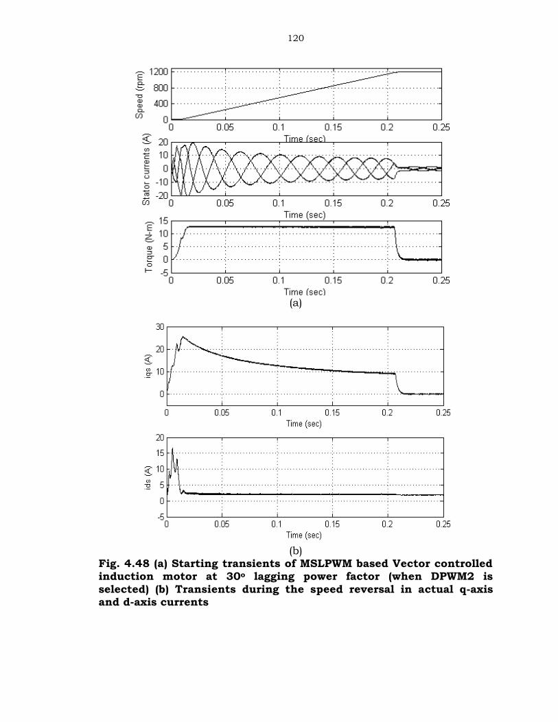
(b)Fig. 4.48 (a) Starting transients of MSLPWM based Vector controlledinduction motor at 30o lagging power factor (when DPWM2 isselected) (b) Transients during the speed reversal in actual q-axisand d-axis currents
121
(a)
(b)
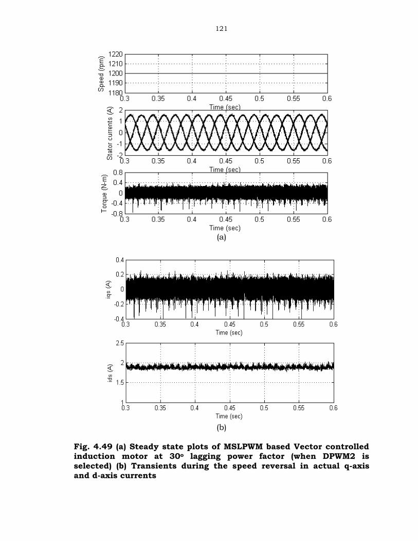
Fig. 4.49 (a) Steady state plots of MSLPWM based Vector controlledinduction motor at 30o lagging power factor (when DPWM2 isselected) (b) Transients during the speed reversal in actual q-axisand d-axis currents
122
(a)
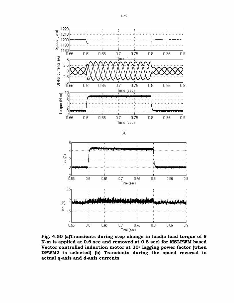
Fig. 4.50 (a)Transients during step change in load(a load torque of 8N-m is applied at 0.6 sec and removed at 0.8 sec) for MSLPWM basedVector controlled induction motor at 30o lagging power factor (whenDPWM2 is selected) (b) Transients during the speed reversal inactual q-axis and d-axis currents
123
(a)
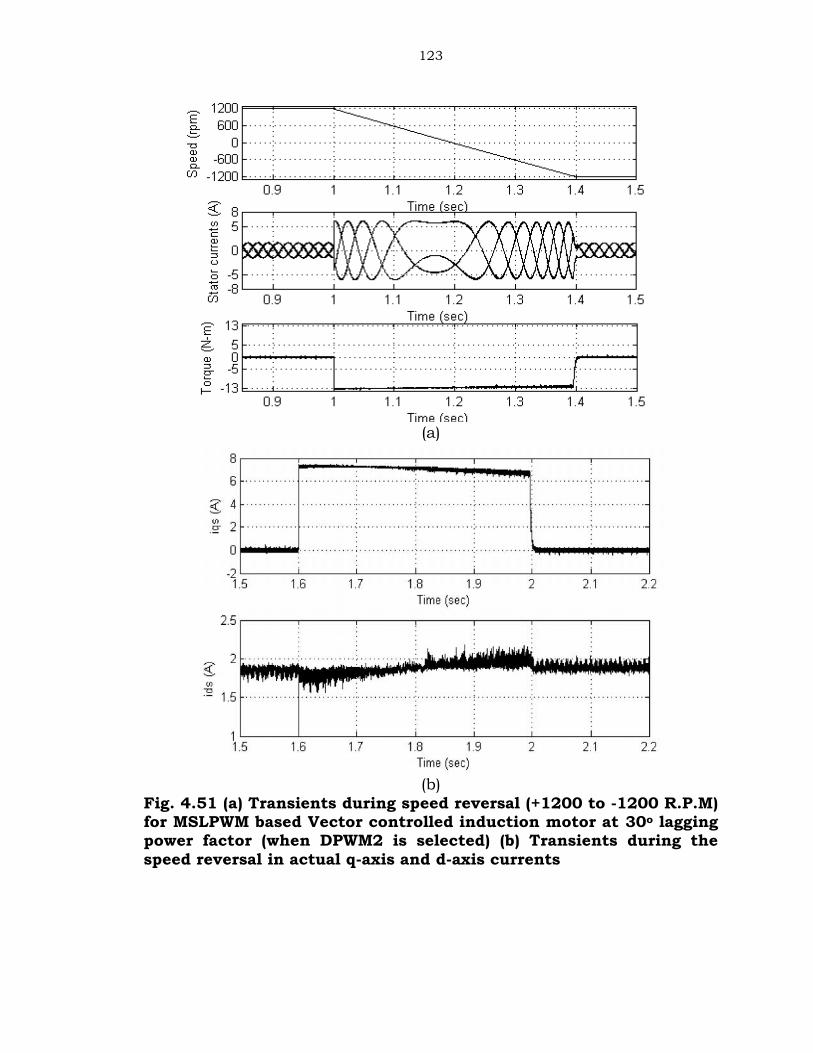
(b)Fig. 4.51 (a) Transients during speed reversal (+1200 to -1200 R.P.M)for MSLPWM based Vector controlled induction motor at 30o laggingpower factor (when DPWM2 is selected) (b) Transients during thespeed reversal in actual q-axis and d-axis currents
124
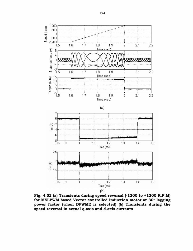
(a)
(b)Fig. 4.52 (a) Transients during speed reversal (-1200 to +1200 R.P.M)for MSLPWM based Vector controlled induction motor at 30o laggingpower factor (when DPWM2 is selected) (b) Transients during thespeed reversal in actual q-axis and d-axis currents
125
Fig 4.45 shows the transients of MSLPWM based drive during the
step change in load condition. The transients during the speed reversal
for proposed MSLPWM based drive at UPF are shown in Fig. 4.46 and
Fig. 4.47. Fig. 4.48 shows the starting transients of MSLPWM based
vector controlled induction motor drive at 30o lagging power factor
conditions. The steady state plots of proposed MSLPWM based vector
controlled induction motor drive are shown in Fig 4.49 at 30o lagging
power factor condition. Fig 4.50 shows the transients of MSLPWM based
drive during the step change in load condition. The transients during the
speed reversal for proposed MSLPWM based drive at 30o lagging power
factor are shown in Fig. 4.51 and Fig. 4.52. From the above results it can
be observed that there is a change in stator current by applying a load
torque of 8 N-m. Also there is a change in stator current as well as in
torque during speed reversal case. From the q-axis and d-axis currents,
it can be observed that the q-axis current is changing according to the
torque requirement and d-axis current is almost constant at all operating
conditions. The THD of line currents of the proposed algorithms are
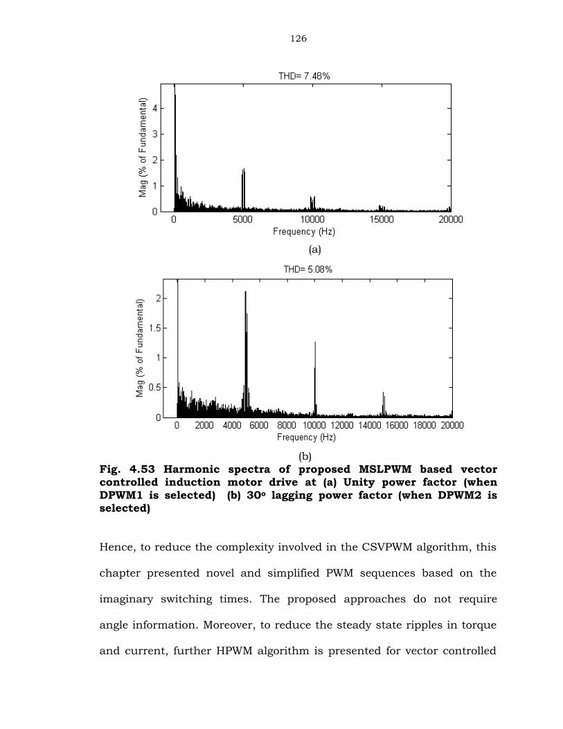
shown in Fig. 4.53.
4.7 Summary:
The indirect vector control algorithm with hysteresis type current
controllers gives more steady state ripple and variable switching
frequency operation. To overcome this problem, the CVSPWM algorithm
has been used traditionally, which needs angle and sector information.
126
(a)
(b)Fig. 4.53 Harmonic spectra of proposed MSLPWM based vectorcontrolled induction motor drive at (a) Unity power factor (whenDPWM1 is selected) (b) 30o lagging power factor (when DPWM2 isselected)
Hence, to reduce the complexity involved in the CSVPWM algorithm, this
chapter presented novel and simplified PWM sequences based on the
imaginary switching times. The proposed approaches do not require
angle information. Moreover, to reduce the steady state ripples in torque
and current, further HPWM algorithm is presented for vector controlled
127
induction motor drive. The proposed HPWM algorithm uses the existing
DPWM algorithms in conjunction with the CSVPWM algorithm. Finally,
the switching loss analysis for the various PWM algorithms is carried out
and MSLPWM algorithm is developed for the vector controlled induction
motor drive. The harmonic spectra of stator currents for MSLVPWM
based vector control of induction motor along with their total harmonic
distortion (THD) values are shown in Fig. 4.53. Thus, the proposed PWM
algorithms reduce the harmonic distortion and switching losses of the
inverter.