Embed Size (px)
Citation preview
PHYSICS MATHEMATICS AND ASTRONOMY DIVISION
CALIFORNIA INSTITUTE OF TECHNOLOGY
Sophomore Physics Laboratory (PH005/105)
Analog ElectronicsActive Filters
Copyright c©Virgínio de Oliveira Sannibale, 2003(Revision December 2012)
DRAFT
Chapter 6
Active Filters
Introduction
An electronic circuit that modifies the frequency spectrum of an arbitrarysignal is called filter. A filter that modifies the spectrum producing ampli-fication is said to be an active filter. Vis à vis its definition, it is convenientto study the filter characteristics in terms of the frequency response of itsassociated two port network
H(ω) =Vo(ω)
Vi(ω),
where Vi and Vo are respectively the input voltage and the output voltageof the network, and ω the angular frequency. Depending on the design,active filters have some important advantages:
• they can provide gain,
• they can provide isolation because of the typical characteristic impedancesof amplifiers,
• they can be cascaded because of the typical characteristic impedancesof amplifiers,
• they can avoid the use of inductors greatly simplifying the design ofthe filters.
Here some disadvantages:
127
DRAFT
128 CHAPTER 6. ACTIVE FILTERS
• they are limited by the amplifiers’ band-with, and noise,
• they need power supplies,
• they dissipate more heat than a passive circuit.
Let’s make some simple definitions useful to classify different types offilters.
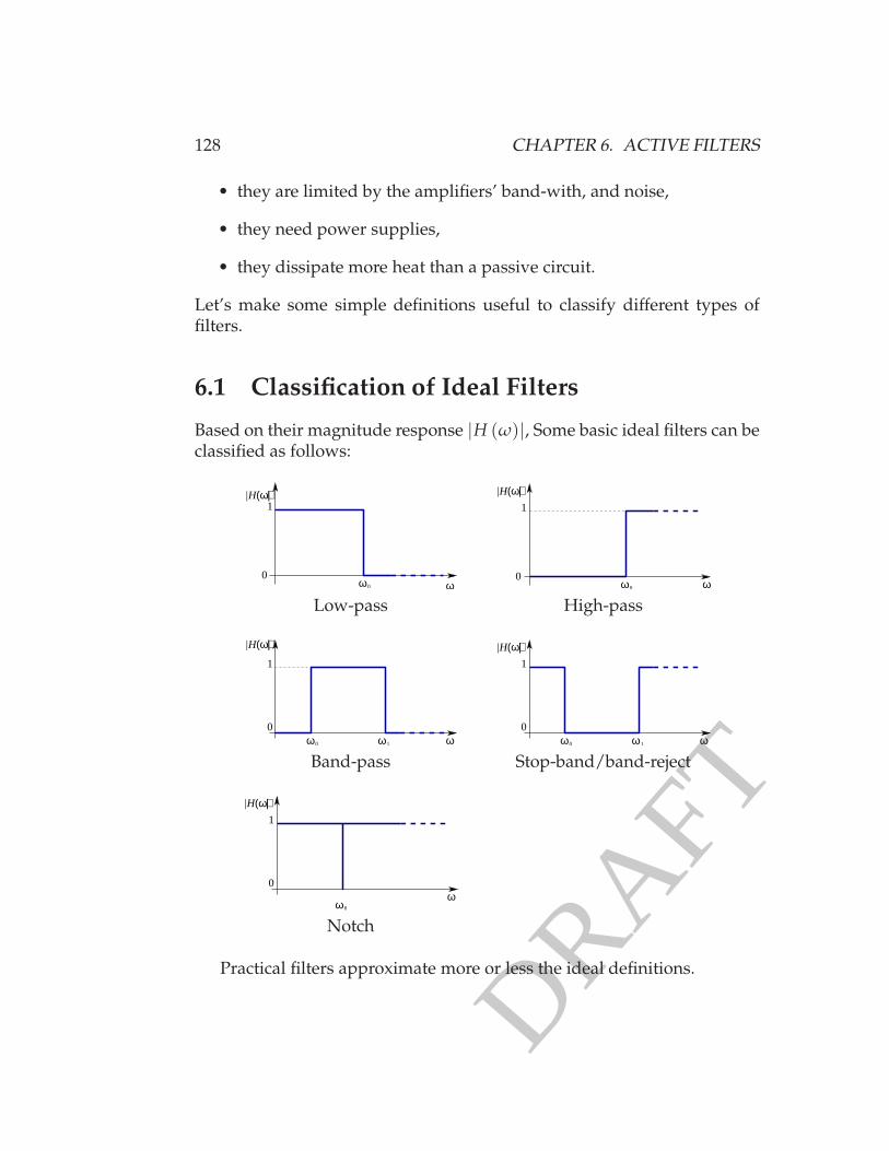
6.1 Classification of Ideal Filters
Based on their magnitude response |H (ω)|, Some basic ideal filters can beclassified as follows:
ω0
(ω)||H
0ω
1 1
(ω)||H
ω0
0ω
Low-pass High-pass
ω0 ω1
|H(ω)|
ω
1
0ω0 ω1
|H(ω)|
ω
1
0
Band-pass Stop-band/band-reject
|H(ω)|
ω0
ω
1
0
Notch
Practical filters approximate more or less the ideal definitions.
DRAFT
6.2. FILTERS AS RATIONAL FUNCTIONS 129
ω2 ω3 ω4 ω5 ω6 ω7ω8ω1
A2
A3
A1
DA1
DA2
DA3
ω
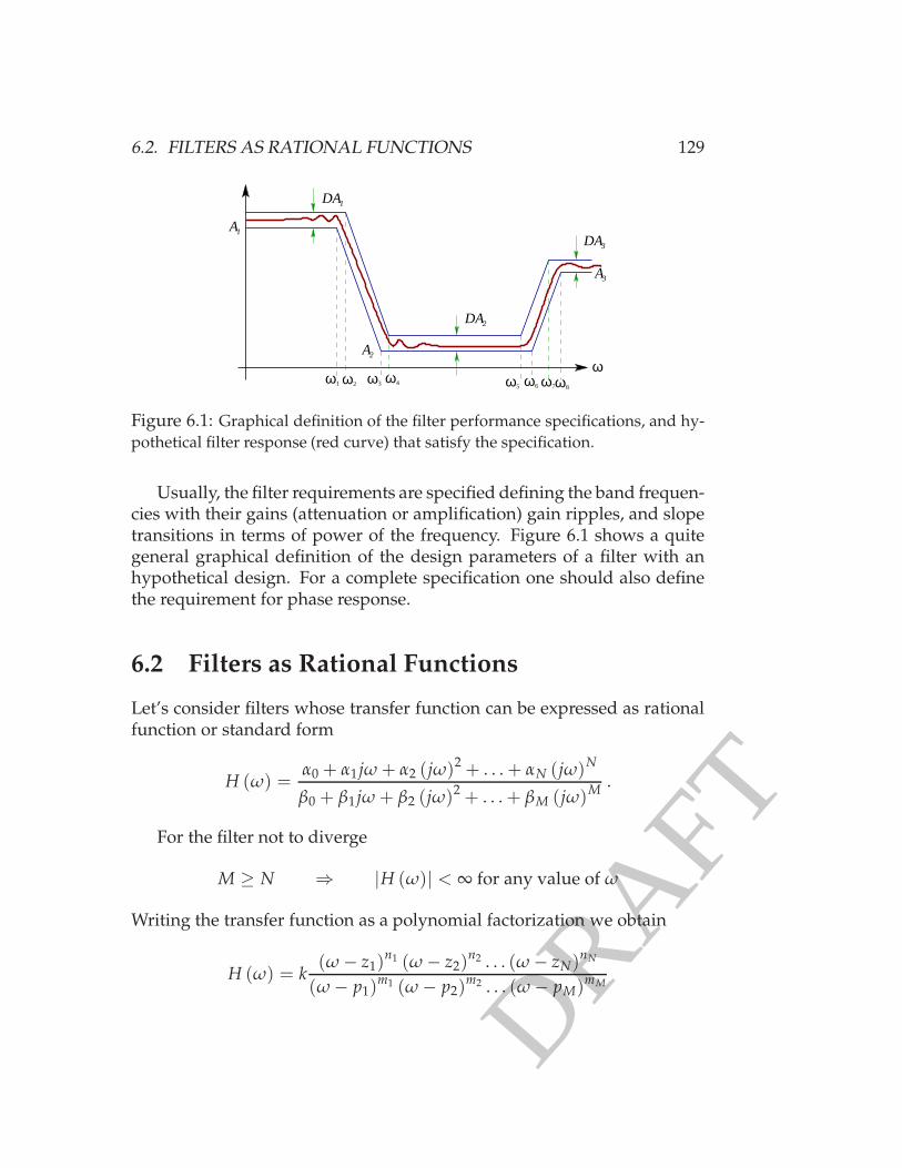
Figure 6.1: Graphical definition of the filter performance specifications, and hy-pothetical filter response (red curve) that satisfy the specification.
Usually, the filter requirements are specified defining the band frequen-cies with their gains (attenuation or amplification) gain ripples, and slopetransitions in terms of power of the frequency. Figure 6.1 shows a quitegeneral graphical definition of the design parameters of a filter with anhypothetical design. For a complete specification one should also definethe requirement for phase response.
6.2 Filters as Rational Functions
Let’s consider filters whose transfer function can be expressed as rationalfunction or standard form
H (ω) =α0 + α1 jω + α2 (jω)2 + . . . + αN (jω)N
β0 + β1 jω + β2 (jω)2 + . . . + βM (jω)M.
For the filter not to diverge
M ≥ N ⇒ |H (ω)| < ∞ for any value of ω
Writing the transfer function as a polynomial factorization we obtain
H (ω) = k(ω − z1)
n1 (ω − z2)n2 . . . (ω − zN)
nN
(ω − p1)m1 (ω − p2)
m2 . . . (ω − pM)mM
DRAFT
130 CHAPTER 6. ACTIVE FILTERS
Denominator roots p1, p2, . . . , pn are called poles, and numerator rootsz1, z2, . . . , zm are called zeros. The integers n1, n2, . . . , nN, and m1, m2, . . . , mN
are therefore the multiplicity of poles and zeros.
Poles and zeros values determine the shape of the filter, and apart fromzero frequency, one could say that poles provide attenuation and zerosamplification.
The transition from transmission to attenuation, and vice versa, in thefilter magnitude |H (ω)| is characterized by an asymptote slope which de-termine the so called filter order.
For example, considering the RC low pass filter with ω0 = 1/RC, wehave one pole p1 = jω0
H (ω) =ω0
ω0 + jω⇒ first oder low pass filter with cut-off freq. ω0
For the RC high pass filter with ω0 = 1/RC, we have one pole p1 = jω0and one zero z1 = 0
H (ω) =ω
ω0 + jω⇒ first oder high pass filter with cut-off freq. ω0
In the next sub-sections, we will analyze into more details filters withthe following transfer function
H (ω) = H0
−ω2 + jωω1
Q1+ ω2
1
−ω2 + jωω0
Q+ ω2
0
DRAFT
6.2. FILTERS AS RATIONAL FUNCTIONS 131
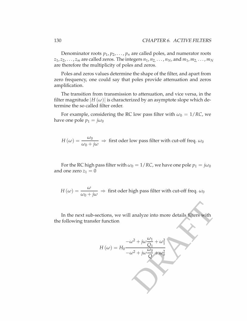
6.2.1 Second Order Low-Pass Filter
Figure below shows the second order low pass filter bode plot, with reso-nant frequency ωres, and characteristic frequency ω0
102
103
104
−40
−30
−20
−10
0
10
Mag
nitu
de [d
B]
ωres
Hmax
ω0
102
103
104
−150
−100
−50
0
Frequency [rad/s]
Pha
se [D
eg]
ωres
φres
ω0
−90
Filterω
resω
0
The second order low-pass filter written in standard form
Transfer Function Resonance Maximum DC High Freq.Gain Gain
H0ω2
0
−ω2 + jωω0
Q+ ω2
0
ω0
√
1 − 12Q2 H0
Q√
1 − 14Q2
H0 0
DRAFT
132 CHAPTER 6. ACTIVE FILTERS
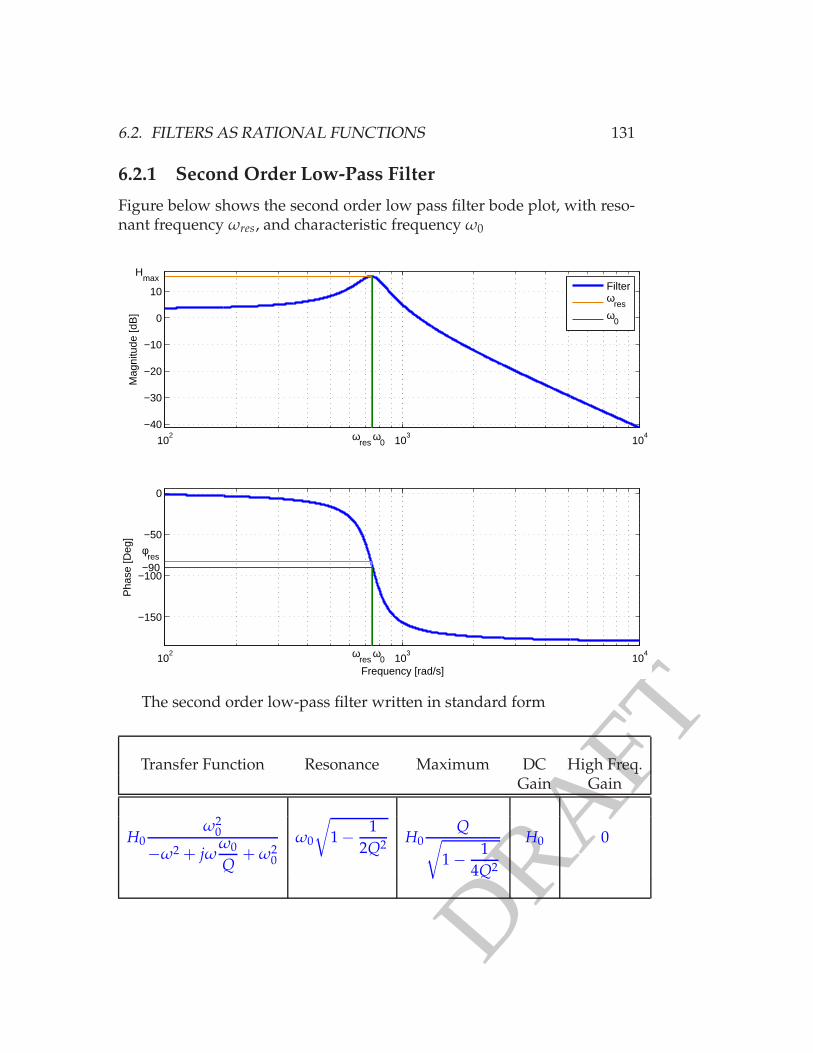
6.2.2 Second Order High-Pass Filter
102
103
104
−30
−20
−10
0
10
Mag
nitu
de [d
B]
ωres
Hmax
ω0
102
103
104
0
50
100
150
Frequency [rad/s]
Pha
se [D
eg]
ωres
φres
ω0
90
Filterω
resω
0
The second order high-pass filter written in standard form
Transfer Function Resonance Maximum DC High Freq.Gain Gain
H0ω2
−ω2 + jωω0
Q+ ω2
0
ω0√
1 − 12Q2
H0Q
√
1 − 14Q
0 H0
DRAFT
6.2. FILTERS AS RATIONAL FUNCTIONS 133
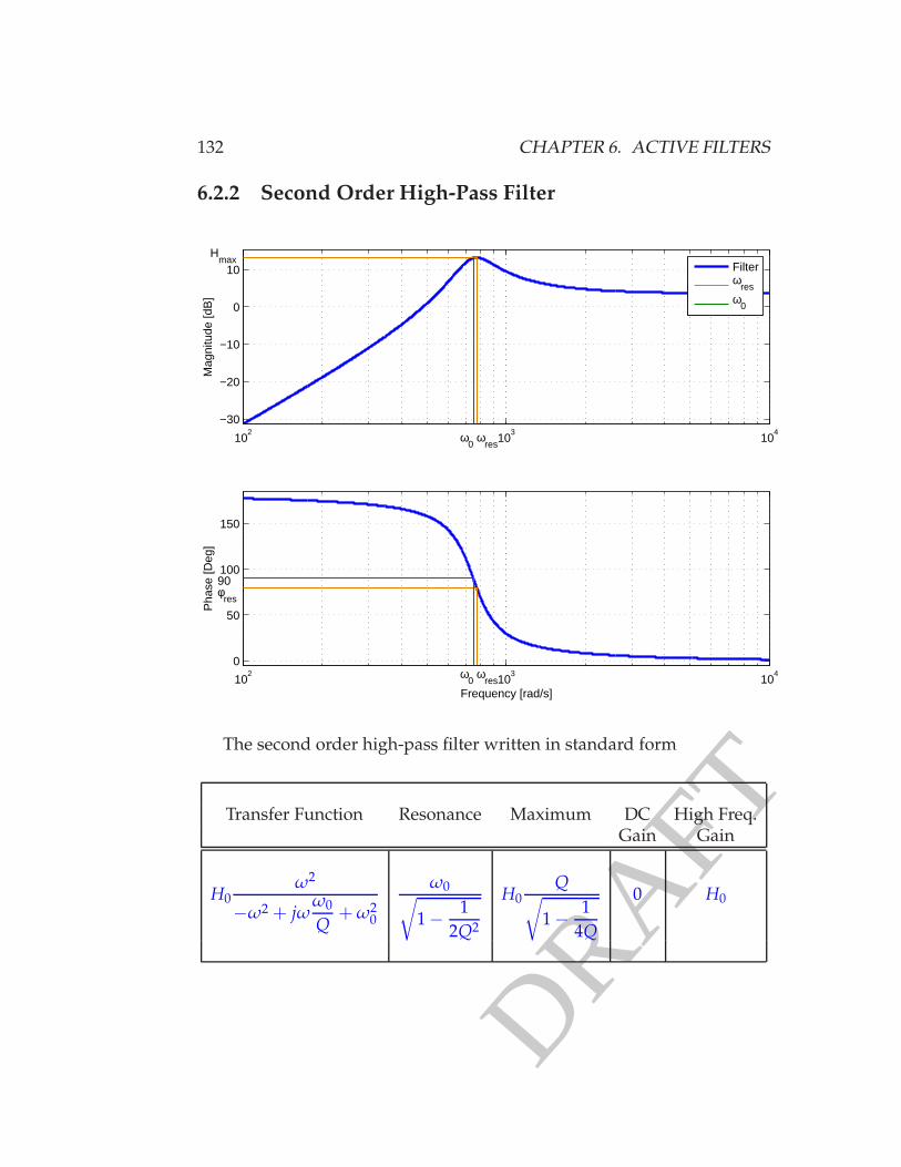
6.2.3 Band-Pass Filter
102
103
104
−30
−25
−20
−15
−10
−5
0
5
Mag
nitu
de [d
B]
ωres
Hmax
ω0
102
103
104
−50
0
50
Frequency [rad/s]
Pha
se [D
eg]
ωres
φres
ω0
0
Filterω
resω
0
The band-pass filter written in standard form is
Transfer Function Resonance Maximum DC Gain High Freq.Gain
H0
jωω0
Q
−ω2 + jωω0
Q+ ω2
0
ω0 H0 0 0
DRAFT
134 CHAPTER 6. ACTIVE FILTERS
For example, depending on the output we consider, the already stud-ied LRC series circuit is a low-pass, a band-pass, or a high-pass filter withthe transfer function described above. When we will study difference fil-ters topologies we will reduce their transfer function into one of the stan-dard form above.
6.3 Common Circuit Filters Topologies
This is a brief and not exhaustive at all list of filter topologies that useresistors, capacitors, and operational amplifiers to implement the filterstypes described above:
• Infinite gain, multiple feedback (IGMF)
• Generalized Sallen-Key (GSK)
• State Variable (SV)
• Switched Capacitor Filters (SC)
Cascading these implementation allows to increase the filter order.
DRAFT
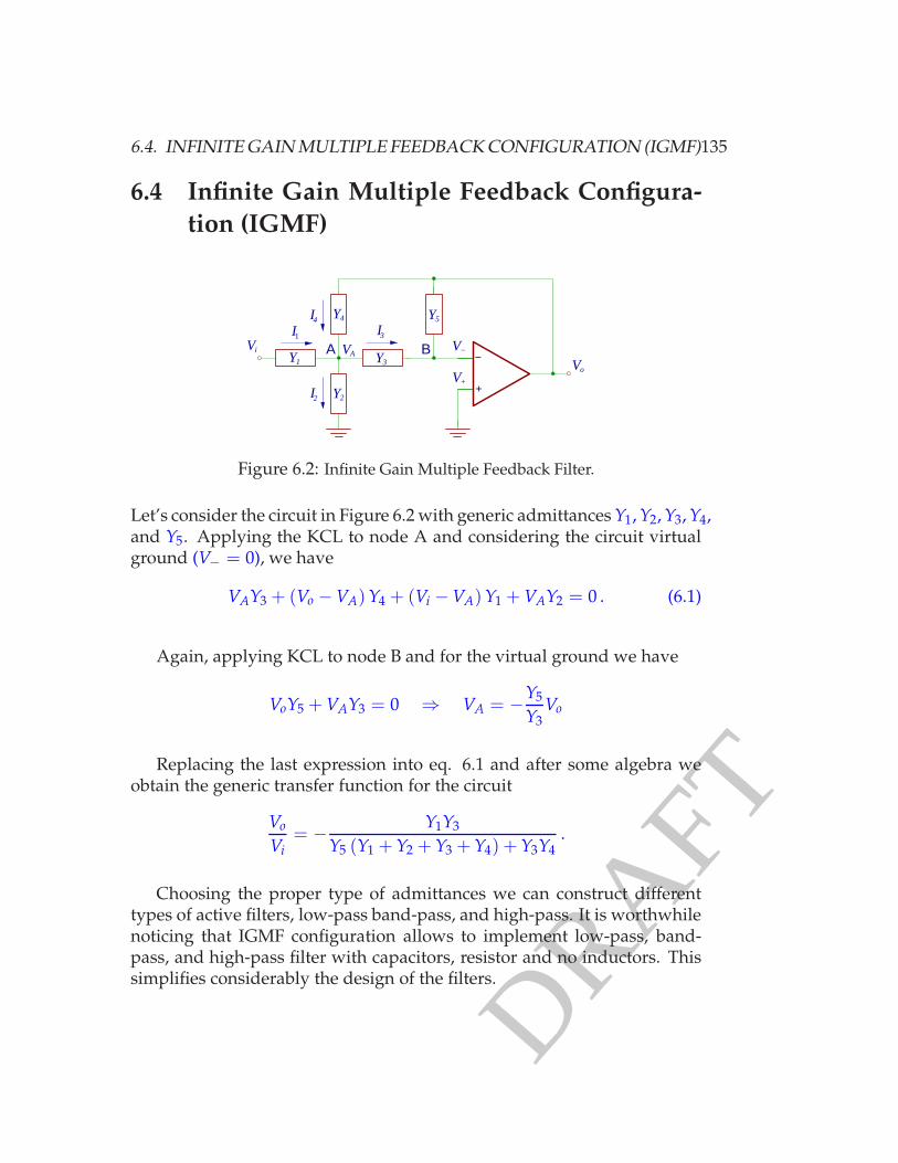
6.4. INFINITE GAIN MULTIPLE FEEDBACK CONFIGURATION (IGMF)135
6.4 Infinite Gain Multiple Feedback Configura-
tion (IGMF)
Vi
Vo
VA
Y4 Y5
Y2
Y3Y1
V−
V+
A B−
+
I1I
I
I2
4
3
Figure 6.2: Infinite Gain Multiple Feedback Filter.
Let’s consider the circuit in Figure 6.2 with generic admittances Y1, Y2, Y3, Y4,and Y5. Applying the KCL to node A and considering the circuit virtualground (V− = 0), we have
VAY3 + (Vo − VA)Y4 + (Vi − VA)Y1 + VAY2 = 0 . (6.1)
Again, applying KCL to node B and for the virtual ground we have
VoY5 + VAY3 = 0 ⇒ VA = −Y5
Y3Vo
Replacing the last expression into eq. 6.1 and after some algebra weobtain the generic transfer function for the circuit
Vo
Vi= − Y1Y3
Y5 (Y1 + Y2 + Y3 + Y4) + Y3Y4.
Choosing the proper type of admittances we can construct differenttypes of active filters, low-pass band-pass, and high-pass. It is worthwhilenoticing that IGMF configuration allows to implement low-pass, band-pass, and high-pass filter with capacitors, resistor and no inductors. Thissimplifies considerably the design of the filters.
DRAFT
136 CHAPTER 6. ACTIVE FILTERS
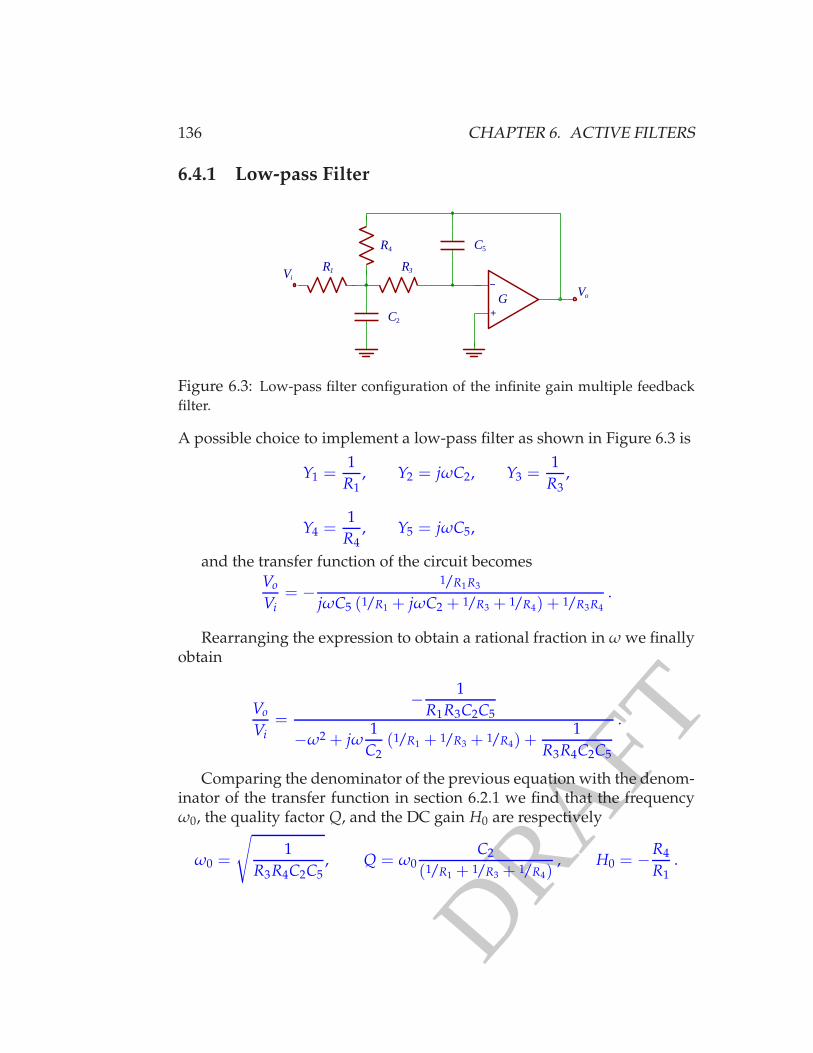
6.4.1 Low-pass Filter
ViR3R1
R4 C5
C2
VoG−
+
Figure 6.3: Low-pass filter configuration of the infinite gain multiple feedbackfilter.
A possible choice to implement a low-pass filter as shown in Figure 6.3 is
Y1 =1
R1, Y2 = jωC2, Y3 =
1R3
,
Y4 =1
R4, Y5 = jωC5,
and the transfer function of the circuit becomesVo
Vi= −
1/R1R3
jωC5 (1/R1 + jωC2 + 1/R3 + 1/R4) + 1/R3R4.
Rearranging the expression to obtain a rational fraction in ω we finallyobtain
Vo
Vi=
− 1R1R3C2C5
−ω2 + jω1
C2(1/R1 + 1/R3 + 1/R4) +
1R3R4C2C5
.
Comparing the denominator of the previous equation with the denom-inator of the transfer function in section 6.2.1 we find that the frequencyω0, the quality factor Q, and the DC gain H0 are respectively
ω0 =
√
1R3R4C2C5
, Q = ω0C2
(1/R1 + 1/R3 + 1/R4), H0 = −R4
R1.
DRAFT
6.4. INFINITE GAIN MULTIPLE FEEDBACK CONFIGURATION (IGMF)137
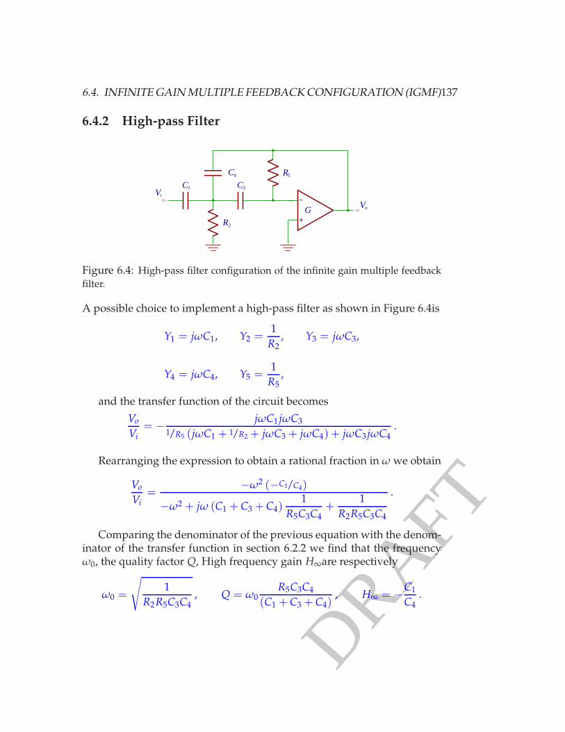
6.4.2 High-pass Filter
Vi
Vo
C1 C3
C4
R
R5
G−
+2
Figure 6.4: High-pass filter configuration of the infinite gain multiple feedbackfilter.
A possible choice to implement a high-pass filter as shown in Figure 6.4is
Y1 = jωC1, Y2 =1
R2, Y3 = jωC3,
Y4 = jωC4, Y5 =1
R5,
and the transfer function of the circuit becomes
Vo
Vi= − jωC1 jωC3
1/R5 (jωC1 + 1/R2 + jωC3 + jωC4) + jωC3 jωC4.
Rearranging the expression to obtain a rational fraction in ω we obtain
Vo
Vi=
−ω2 (−C1/C4)
−ω2 + jω (C1 + C3 + C4)1
R5C3C4+
1R2R5C3C4
.
Comparing the denominator of the previous equation with the denom-inator of the transfer function in section 6.2.2 we find that the frequencyω0, the quality factor Q, High frequency gain H∞are respectively
ω0 =
√
1R2R5C3C4
, Q = ω0R5C3C4
(C1 + C3 + C4), H∞ = −C1
C4.
DRAFT
138 CHAPTER 6. ACTIVE FILTERS
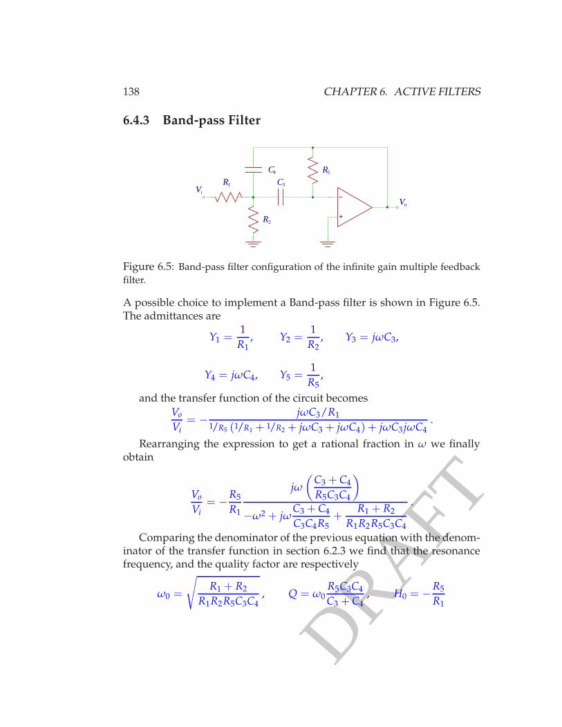
6.4.3 Band-pass Filter
−
+
Vi
Vo
C4 R5
R2
R1 C3
Figure 6.5: Band-pass filter configuration of the infinite gain multiple feedbackfilter.
A possible choice to implement a Band-pass filter is shown in Figure 6.5.The admittances are
Y1 =1
R1, Y2 =
1R2
, Y3 = jωC3,
Y4 = jωC4, Y5 =1
R5,
and the transfer function of the circuit becomesVo
Vi= − jωC3/R1
1/R5 (1/R1 + 1/R2 + jωC3 + jωC4) + jωC3 jωC4.
Rearranging the expression to get a rational fraction in ω we finallyobtain
Vo
Vi= −R5
R1
jω
(
C3 + C4
R5C3C4
)
−ω2 + jωC3 + C4
C3C4R5+
R1 + R2
R1R2R5C3C4
.
Comparing the denominator of the previous equation with the denom-inator of the transfer function in section 6.2.3 we find that the resonancefrequency, and the quality factor are respectively
ω0 =
√
R1 + R2
R1R2R5C3C4, Q = ω0
R5C3C4
C3 + C4, H0 = −R5
R1
DRAFT
6.5. GENERALIZED SALLEN-KEY FILTER TOPOLOGY (GSK) 139
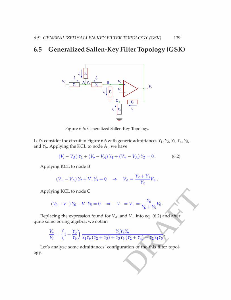
6.5 Generalized Sallen-Key Filter Topology (GSK)
Vo
V+
V−
Y6
I6Y5
Vi VA
Y4
Y2Y1
I3I4
Y3I3
+
−
A BI1
C
I5
Figure 6.6: Generalized Sallen-Key Topology.
Let’s consider the circuit in Figure 6.6 with generic admittances Y1, Y2, Y3, Y4, Y5,and Y6. Applying the KCL to node A , we have
(Vi − VA)Y1 + (Vo − VA)Y4 + (V+ − VA)Y2 = 0 . (6.2)
Applying KCL to node B
(V+ − VA)Y2 + V+Y3 = 0 ⇒ VA =Y2 + Y3
Y2V+ .
Applying KCL to node C
(V0 − V−)Y6 − V−Y5 = 0 ⇒ V− = V+ =Y6
Y6 + Y5V0 .
Replacing the expression found for VA, and V+ into eq. (6.2) and afterquite some boring algebra, we obtain
Vo
Vi=
(
1 +Y5
Y6
)
Y1Y2Y6
Y1Y6 (Y2 + Y3) + Y3Y6 (Y2 + Y4)− Y2Y4Y5.
Let’s analyze some admittances’ configuration of the this filter topol-ogy.
DRAFT
140 CHAPTER 6. ACTIVE FILTERS
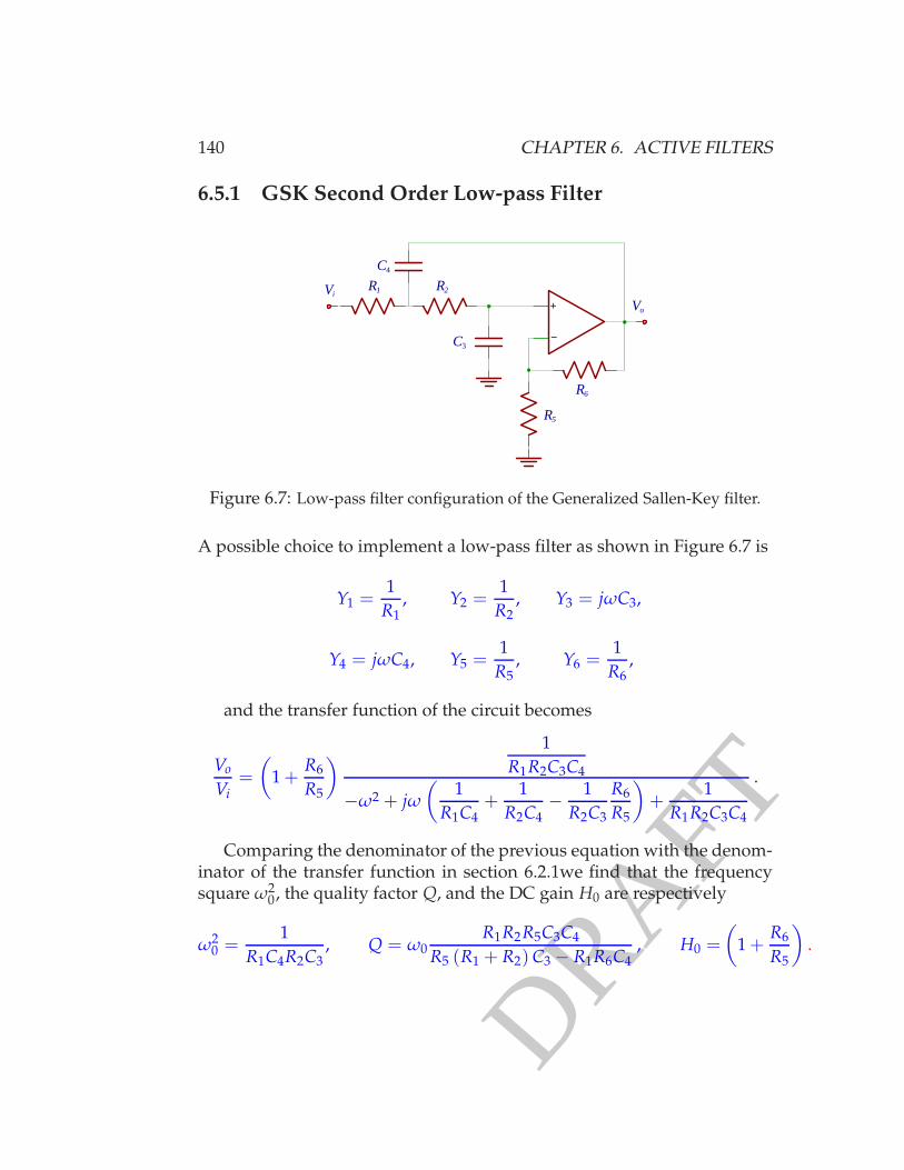
6.5.1 GSK Second Order Low-pass Filter
R2Vi
Vo
R6
C4
C3
R1
R5
+
−
Figure 6.7: Low-pass filter configuration of the Generalized Sallen-Key filter.
A possible choice to implement a low-pass filter as shown in Figure 6.7 is
Y1 =1
R1, Y2 =
1R2
, Y3 = jωC3,
Y4 = jωC4, Y5 =1
R5, Y6 =
1R6
,
and the transfer function of the circuit becomes
Vo
Vi=
(
1 +R6
R5
)
1R1R2C3C4
−ω2 + jω
(
1R1C4
+1
R2C4− 1
R2C3
R6
R5
)
+1
R1R2C3C4
.
Comparing the denominator of the previous equation with the denom-inator of the transfer function in section 6.2.1we find that the frequencysquare ω2
0, the quality factor Q, and the DC gain H0 are respectively
ω20 =
1R1C4R2C3
, Q = ω0R1R2R5C3C4
R5 (R1 + R2)C3 − R1R6C4, H0 =
(
1 +R6
R5
)
.
DRAFT
6.5. GENERALIZED SALLEN-KEY FILTER TOPOLOGY (GSK) 141
6.5.2 Simple Case
If R1 = R2 = R, C3 = C4 = C, and R5 = R6 = 0, then
Vo
Vi=
ω20
−ω2 + jωω0 + ω20
, ω20 =
1R2C2 , , Q = 1 ,
which is the transfer function of a second order low-pass filter with lowquality factor.
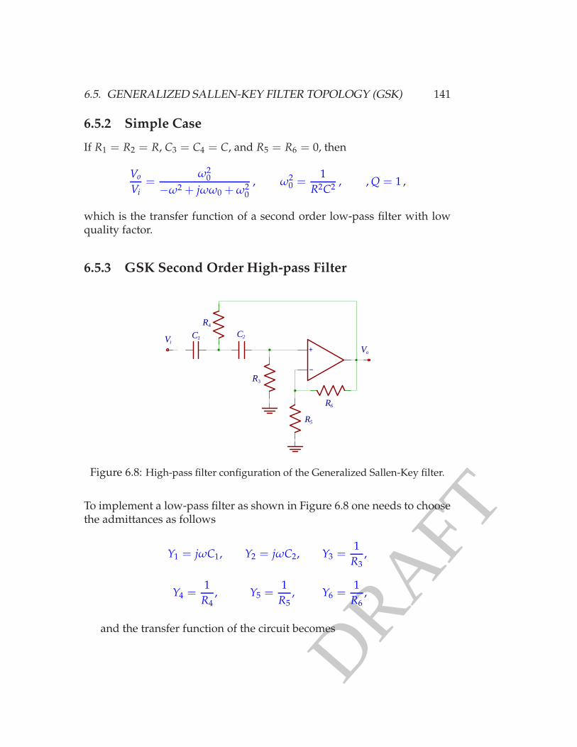
6.5.3 GSK Second Order High-pass Filter
Vi
Vo
R6
R5
R4
C2C1
R3
+
−
Figure 6.8: High-pass filter configuration of the Generalized Sallen-Key filter.
To implement a low-pass filter as shown in Figure 6.8 one needs to choosethe admittances as follows
Y1 = jωC1, Y2 = jωC2, Y3 =1
R3,
Y4 =1
R4, Y5 =
1R5
, Y6 =1
R6,
and the transfer function of the circuit becomes
DRAFT
142 CHAPTER 6. ACTIVE FILTERS
Vo
Vi=
(
1 +R6
R5
) −ω2
−ω² + jω
(
1R3C2
+1
R3C1− 1
R4C1
R6
R5
)
+1
R3R4C1C2
.
Comparing the denominator of the previous equation with the denom-inator of the transfer function in section 6.2.2 we find that the frequencysquare ω2
0, the quality factor Q, and the DC gain H0 are respectively
ω20 =
1R3C1R4C2
, Q = ω0R3R4R5C1C2
R5 (C1 + C2) R3 − C1R6R4, H0 =
(
1 +R6
R5
)
.
6.5.4 Simple Case
If R1 = R2 = R, C3 = C4 = C, and R5 = R6 = 0, then
Vo
Vi=
−ω2
−ω2 + jωω0 + ω20
, ω20 =
1R2C2 , , Q = 1 ,
which is the transfer function of a second order high-pass filter with lowquality factor.
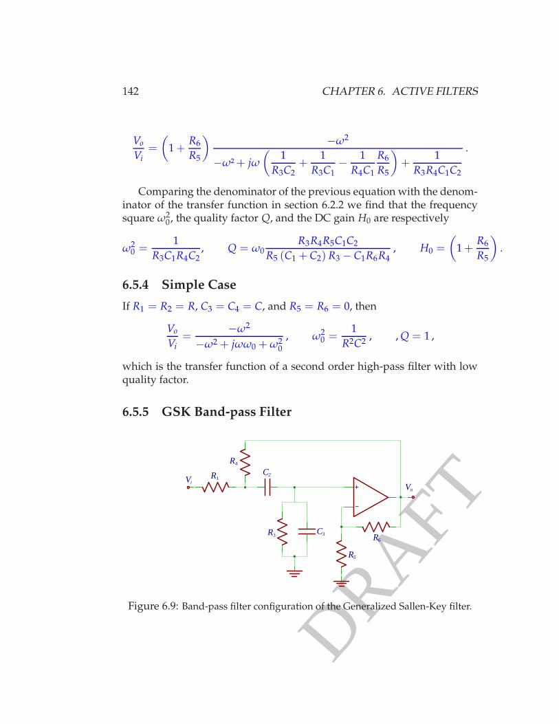
6.5.5 GSK Band-pass Filter
R4
C2
C3
Vo
ViR1
R3 R6
R5
+
−
Figure 6.9: Band-pass filter configuration of the Generalized Sallen-Key filter.
DRAFT
6.5. GENERALIZED SALLEN-KEY FILTER TOPOLOGY (GSK) 143
To implement a band-pass filter as shown in Figure 6.9 one needs to choosethe admittances as follows
Y1 =1
R1, Y2 = jωC2, Y3 =
1R3
+ jωC3,
Y4 =1
R4, Y5 =
1R5
, Y6 =1
R6,
and the transfer function of the circuit becomes
Vo
Vi=
(
1 +R6
R5
)
jω
R1C3
−ω2 + jω
(
C2 + C3
C2C3R1+
1C3R3
+1
C2R4− 1
C3R4
R6
R5
)
+R1 + R4
C2C3R1R3R4
.
Comparing the denominator of the previous equation with the denom-inator of the transfer function in section 6.2.3 we find that the frequencysquare ω2
0, the quality factor Q, and the DC gain H0 are respectively
Q = ω0C2C3R1R3R4R5
(C2 + C3) R3R4R5 + C2R1R4R5 + C3R1R3R5 − C2R1R3R6,
ω20 =
R1 + R4
C2C3R1R3R4,H0 =
1R1C3
(
1 +R6
R5
)
Q
ω0.
6.5.6 Simple Case
If R1 = R3 = R4 = R, C2 = C3 = C, and R5 = R6 = 0, then
Vo
Vi=
jωω0
Q
−ω2 + jωω0
Q+ ω2
0
, ω0 =
√2
RC, , Q =
√2
3,
which is the transfer function of a second order high-pass filter with lowquality factor.
DRAFT
144 CHAPTER 6. ACTIVE FILTERS
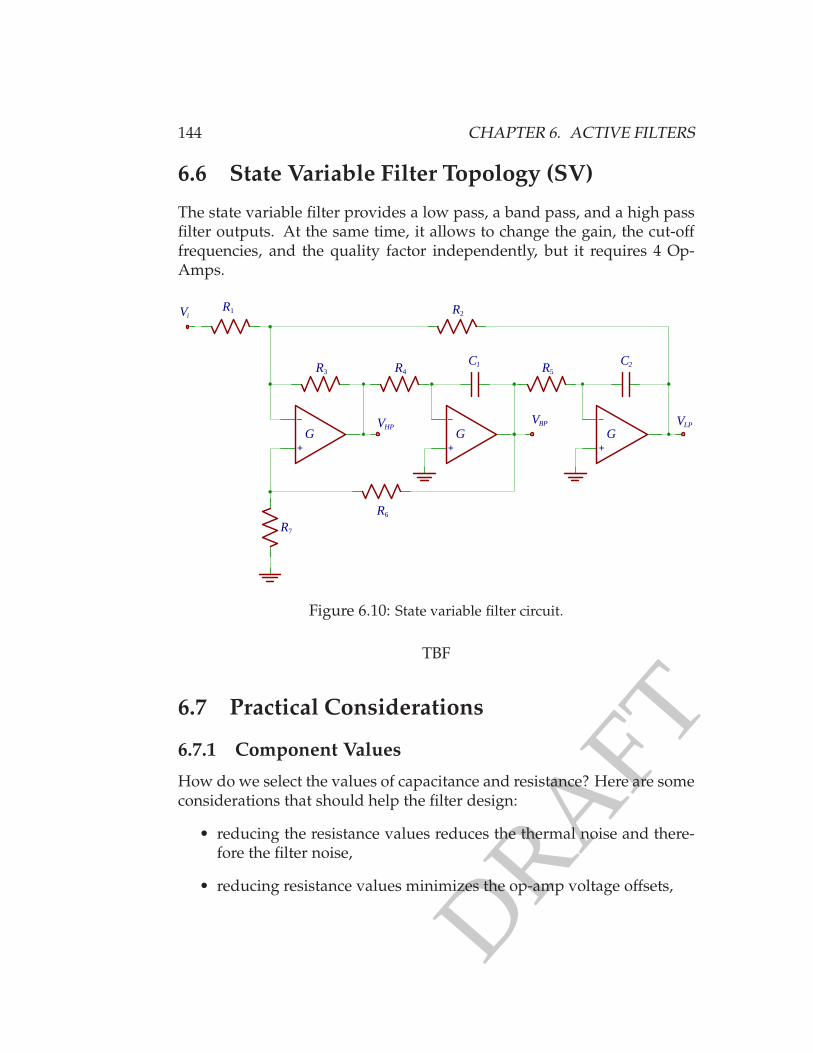
6.6 State Variable Filter Topology (SV)
The state variable filter provides a low pass, a band pass, and a high passfilter outputs. At the same time, it allows to change the gain, the cut-offfrequencies, and the quality factor independently, but it requires 4 Op-Amps.
R1Vi
G−
+
VHPVBP
G−
+
C1
R7
R6
R2
VLP
G−
+
C2R3 R4 R5
Figure 6.10: State variable filter circuit.
TBF
6.7 Practical Considerations
6.7.1 Component Values
How do we select the values of capacitance and resistance? Here are someconsiderations that should help the filter design:
• reducing the resistance values reduces the thermal noise and there-fore the filter noise,
• reducing resistance values minimizes the op-amp voltage offsets,
DRAFT
6.7. PRACTICAL CONSIDERATIONS 145
• increasing the resistance reduce the current load on the op-amps,
• increasing the resistances usually allows to decrease the capacitanceand therefore it make easier to find capacitors because of the smallcapacitance values needed,
• reducing the capacitance minimizes the capacitance fluctuations dueto temperature,
• increasing the capacitance allows to reduce resistance values andtherefore the thermal noise.
As we can clearly see, some of the consideration cannot be used at thesame time. Based on the design requirements one can decide which of theconsideration above are more important to finally meet the design require-ments.
Rules of Thumb
Particularly critical design often overrule these following rules:
• Capacitor with capacitance less of ~100 pF should be avoided,
• Try to use resistor with resistance between few kilo-ohms to few hun-dreds of kilo-ohms.
6.7.2 Components technology
Capacitors
The use of low loss dielectric is very important to obtain good results.If possible one should use plastic film capacitors or C0G/NPO ceramiccapacitors, 1% tolerance for temperature stability.
Resistor
Low thermal noise resistors such as metal film resistors 1% tolerance fortemperature stability should be used.

DRAFT
146 CHAPTER 6. ACTIVE FILTERS
DRAFT
Bibliography
[1] Hank Zumbahlen, State Variable Filters, Mini Tutorial MT-223, Ana-log Devices
147

DRAFT
148 BIBLIOGRAPHY