Embed Size (px)
Citation preview
Journal of Alloys and Compounds 582 (2014) 12–21
Contents lists available at ScienceDirect
Journal of Alloys and Compounds
journal homepage: www.elsevier .com/locate / ja lcom
Sonicated sol–gel preparation of nanoparticulate ZnO thin filmswith various deposition speeds: The highly preferred c-axis(002) orientation enhances the final properties
0925-8388/$ - see front matter � 2013 Elsevier B.V. All rights reserved.http://dx.doi.org/10.1016/j.jallcom.2013.07.202
⇑ Corresponding author. Tel.: +60 176027671.E-mail address: [email protected] (M.F. Malek).
M.F. Malek a,⇑, M.H. Mamat a, Z. Khusaimi b, M.Z. Sahdan c, M.Z. Musa a, A.R. Zainun d, A.B. Suriani e,N.D. Md Sin a, S.B. Abd Hamid f, M. Rusop a,b
a NANO-ElecTronic Centre (NET), Faculty of Electrical Engineering, Universiti Teknologi MARA (UiTM), 40450 Shah Alam, Selangor, Malaysiab NANO-SciTech Centre (NST), Institute of Science (IOS), Universiti Teknologi MARA (UiTM), 40450 Shah Alam, Selangor, Malaysiac Microelectronic & Nanotechnology Centre (MiNT), Universiti Tun Hussein Onn Malaysia (UTHM), 86400 Batu Pahat, Johor, Malaysiad Faculty of Electrical & Electronics Engineering, Universiti Malaysia Pahang (UMP), Lebuhraya Tun Razak, 26300 Kuantan, Pahang, Malaysiae Department of Physics, Faculty of Science and Mathematics, Universiti Pendidikan Sultan Idris, 35900 Tanjung Malim, Perak, Malaysiaf Nanotechnology and Catalysis Research Centre (NANOCAT), Universiti Malaya (UM), 50603 Kuala Lumpur, Malaysia
a r t i c l e i n f o
Article history:Received 24 March 2013Received in revised form 31 July 2013Accepted 31 July 2013Available online 8 August 2013
Keywords:ZnOThin filmsSol–gel processesX-ray diffractionStrain
a b s t r a c t
Zinc oxide (ZnO) thin films have been deposited onto glass substrates at various deposition speeds by asonicated sol–gel dip-coating technique. This work studies the effects of deposition speed on the crystal-lisation behaviour and optical and electrical properties of the resulting films. X-ray diffraction (XRD)analysis showed that thin films were preferentially oriented along the (002) c-axis direction of the crys-tal. The transformation sequence of strain and stress effects in ZnO thin films has also been studied. Thefilms deposited at a low deposition speed exhibited a large compressive stress of 0.78 GPa, whichdecreased to 0.43 GPa as the deposition speed increased to 40 mm/min. Interestingly, the enhancementin the crystallinity of these films led to a significant reduction in compressive stress. All films exhibited anaverage transmittance of greater than 90% in the visible region, with absorption edges at �380 nm. Thephotoluminescence (PL) measurements indicated that the intensity of the emission peaks varied signif-icantly with deposition speed. The optical band gap energy (Eg) was evaluated as 3.276–3.289 eV, whichincreased with decreasing compressive stress along the c-axis. The energy band gap of the resulting ZnOfilms was found to be strongly influenced by the preferred c-axis (002) orientation.
� 2013 Elsevier B.V. All rights reserved.
1. Introduction thin films must be fabricated. It is convenient to grown-type ZnO
Zinc oxide (ZnO) materials have recently attracted tremendousattention among researchers due to their wide range of electricaland optical properties. ZnO is a II–VI semiconductor with a wideand direct band gap (3.2–3.4 eV at 300 K), excellent chemical andthermal stability, and the unique electrical and optoelectronicproperty of a large exciton binding energy (60 meV), which couldlead to lasing action even above room temperature [1–3]. Further-more, its tunable band gap and high transparency have made ZnO acandidate material for short-wavelength and transparent optoelec-tronic devices including light-emitting diodes (LEDs) [4,5], solarcells [6], and sensors [7]. These properties and potential applica-tions make this material an excellent subject for theoretical andexperimental studies. Generally, ZnO thin films grow as n-typesemiconductors due to their native defects. To achieve ZnO-baseddevices with the desired characteristics, high quality n-type ZnO
thin films with good electrical properties, as ZnO possesses intrin-sic electron conductivity due to its oxygen vacancies (Vo) and inter-stitial zinc ions (Zni), which act as donors in the crystal lattice. It iswell known that the adsorption and desorption of oxygen on theZnO surface and grain boundaries lead to significant decreasesand increases in the conductivity of ZnO polycrystalline thin films.
ZnO films can be produced in various phases such as wurtzite(hcp), rocksalt (fcc), cesium chloride (sc), and zinc blend (fcc)[8,9]. Under ambient conditions, ZnO crystallises in the wurtzitestructure, a tetrahedrally coordinated structure with a hexagonallattice. ZnO films can crystallise in various orientations as a func-tion of the deposition technique, sol concentration and other fac-tors. A higher c-axis (002) peak orientation indicates theminimisation of the internal stress and free surface energy of thefilms, as well as dense atomic packing. The quality of the film istypically determined by its crystalline orientation, surface unifor-mity, transparency and conductivity [10,11]. Among all of theseparameters, the crystalline orientation is the key to achieving aZnO thin film with piezoelectric properties.

M.F. Malek et al. / Journal of Alloys and Compounds 582 (2014) 12–21 13
Strong preferential growth of ZnO nanocrystals along the c-axis(002) plane suggests a wurtzite structure due to the minimisationof the surface free energy of each crystal plane [12]. Therefore,many researchers have studied the influence of deposition param-eters on the final properties of ZnO thin films, particularly the crys-tal orientation. Bouderbala et al. prepared ZnO films by r.f.sputtering [13], varying the deposition time to obtain differentthicknesses. Their results suggest that the crystallinity is improvedwhen the film thickness increases. On the other hand, XRD analysisshowed that the grains were always oriented according to thec-axis perpendicular to the substrate surface, regardless of thethickness. Ozga and co-workers investigated the photo-inducedsecond harmonic generation (SHG) in Au nanoparticle-depositedZnO nanocrystallite films using coherent bicolour interactions[14]. They found that increasing gold nanoparticle content favoursan enhancement of the output SHG, while the maximum secondorder optical susceptibility was achieved due to the enhancementof the electron–phonon interactions at the interfaces of the nano-crystallites [14,15]. The SHG depended on the degree of crystallin-ity, grain boundaries and film interfaces. The deposition of hexag-onal films with the crystallographic c-axis between the substrateplanes enhanced the susceptibility [14].
Recent studies have reported modifications to these (002) ori-ented thin films to enhance their final properties. Shabannia andAbu Hassan produced ZnO nanorods by a low-temperature chemi-cal bath deposition on a ZnO/PS substrate [16]. The ZnO nanorodsexhibited a high crystallinity with hexagonal wurtzite phases, grewvertically in the (002) direction along the c-axis, and exhibited alow compressive strain (�0.0363%) along this axis. Salam et al. pre-pared intrinsic and aluminum-doped zinc oxide thin films via spincoating over soda-lime glass substrates [17]. They reported that fur-ther increasing the Al doping level to 2 at.% caused a lattice distor-tion due to the difference in the crystallite size between Al and Zn,along with a slight decrease in the preferred (002) orientation.Drmosh et al. developed Cu-doped ZnO (ZnO:Cu) thin films on aglass substrate at room temperature by a pulsed laser deposition(PLD) method [18]. All of the ZnO:Cu films preferentially orientedalong the (002) crystal plane. These authors claimed that the ZnO:-Cu films exhibited a leftward shift in the (002) peak and a de-creased intensity of this peak as the Cu concentration wasincreased. In our previous paper [19], we reported that ZnO filmsstrongly oriented along the (002) plane can be prepared on glasssubstrates by a dip-coating technique. The sol concentration signif-icantly affected the crystal orientation/behaviour and other proper-ties of the final films. Furthermore, a nearly stress- and strain-freethin film was obtained for the film deposited in a highly c-axis ori-ented direction along the (002) plane. Moreover, a higher degree ofcrystallinity along the (002) plane improved the performance ofthe fabricated solar cell [20]. The solar cell device based on Al:ZnOnanorod arrays (highly c-axis oriented) exhibited an efficiency, g, of0.287%, compared with 0.263% for the device based on ZnO nanorodarrays (low c-axis orientation). The current study describes thegrowth process and the effects of the deposition speed on the crys-tal orientation as well as the optical and electrical properties of thefilms. This study also provides a deep understanding of the nanop-articulate growth to obtain more detailed insight into the condi-tions for the formation of highly c-axis oriented ZnO films.
2. Experimental procedures
2.1. Materials preparation
The ZnO sonicated sol–gel was prepared as follows: zinc acetate dihydrate(Zn(CH3COO)2�2H2O) was first dissolved in 2-methoxyethanol (C3H8O2) at roomtemperature. Then, monoethanolamine (MEA, C2H7NO) was added as a solstabiliser. The molar ratio of MEA to zinc acetate was maintained at 1.0, and theconcentration of zinc acetate was 0.4 mol/L. The resulting solution was stirred at80 �C for 1 h to yield a clear and homogeneous solution, which served as the coating
solution. Afterwards, the solution was sonicated at 50 �C for 1 h using an ultrasonicwater bath (Hwasin Technology Powersonic 405, 40 kHz). Finally, the solution wasaged for 24 h before the deposition process. Corning 7740 glass (20 � 20 mm2) wasused as the substrate material. The glass sheets were cleaned twice in an ultrasonicbath with sequences of acetone (5 min), methanol (5 min), and deionised water(5 min). The substrates were subsequently dried by a stream of nitrogen gas andpreserved in a desiccator.
2.2. Film growth deposition
The ZnO films were deposited by dipping a glass substrate into the coating solu-tion and withdrawing it at rates of 10–50 mm/min at room temperature. To facili-tate film thickness measurements, a section of the substrate was covered withadhesive tape, which was subsequently peeled off after the deposition process.The substrates were then heated in a furnace at 300 �C for 10 min to evaporatethe solvent and remove residual organic material. Each sample was subjected tothis procedure five times to obtain an initial five layer film structure. After coatingthe required number of layers, the ZnO thin film was annealed at 500 �C for 1 h be-fore cooling in air to room temperature. Fig. 1 presents a diagram of the sol prepa-ration and deposition process.
2.3. Characterisation
The degree of crystallinity and crystalline orientation of the ZnO thin films wasmeasured using a Bruker AXS D8 Advance X-ray diffractometer (XRD) with Cu Karadiation, k = 1.54 Å. The beam voltage and beam current were 40 kV and 40 mA,respectively. The scan pattern data were collected in a standard h–2h Bragg–Brent-ano geometry configuration between 25� and 60� with a step length of 0.02�. Thesurface morphology of the films was evaluated using a ZEISS Supra 40VP field emis-sion scanning electron microscope (FESEM) with an operating voltage between 0.02and 30 kV. The film thickness was measured using a KLA Tencor P-6 profilometer.UV–Vis–NIR spectroscopy was performed using a Varian Cary 5000 UV–Vis–NIRspectrophotometer over the wavelength range between 300 and 1500 nm with adata interval of 1 nm. The photoluminescence (PL) properties of the synthesisedfilm were measured using a Horiba Jobin Yvon-79 DU420A-OE-325 PL spectropho-tometer with a helium–cadmium (He–Cd) excitation laser source operating at325 nm. The electrical properties were characterised by sheet resistance measure-ments with a two-probe DC system and an Advantest R6243 power supply. Gold(Au) was sputtered as an electrode for current–voltage (I–V) measurements usingan EMITECH K550X sputter coater. The I–V curve of the film was tested to verifythe suitability of the deposited films for use in electronic devices.
3. Results and discussion
3.1. Structural and morphological characterisation
The deposition speed was investigated because the pulling rateaffects the surface morphology and the film thickness. The XRDpatterns of the ZnO thin film for each deposition speed are pre-sented in Fig. 2. The presence of all peaks was indexed to the stan-dard XRD spectrum of the ZnO structure in accordance with JCPDScard No. 00-036-1451. All films exhibited a main peak attributed tothe (002) plane. Other peaks represent low intensity (100) and(101) diffraction peaks. The adhesion of the ZnO thin film to theglass substrate was examined by an ordinary tape peel test using3M Scotch Tape™. None of the films deposited on glass substratesappeared to be removed, indicating strong adherence of the filmsto the glass substrates. Brinker and Scherer claimed that lowerdeposition speeds produce thinner films because the solvent canmore easily evaporate from the film [21,22]. As a result, orientedgrain growth may easily occur in the second layer because of thepresence of slightly oriented grains in the previous layer. There-fore, the strongest preferential orientation along the c-axis is ob-served at 2h = 34.56� for ZnO films deposited at 40 mm/min,which indicates the existence of single phase ZnO with a hexagonalwurtzite structure. The peaks other than that of the (002) planeare very weak. Therefore, the crystallites are highly oriented alongthe c-axis, which is perpendicular to the substrate. Increasing thedeposition speed to 50 mm/min resulted in a slight decrease inthe (002) peak intensity. At higher deposition speeds, thethickness of the film per dip became thicker, and it became moredifficult for the solvent to evaporate, which could disturb the ori-

Fig. 1. Schematic diagram of ZnO thin film preparation procedure at various deposition speeds.
246
246
246
246
25 30 35 40 45 50 55 60
246
(100
)
(101
) (a)
(d)
(e)
(c)
(b)
(002
)
Inte
nsity
(1x
103 c
ount
s/s)
2θ (Degree)
Fig. 2. XRD patterns of ZnO thin films prepared at various deposition speeds: (a)10 mm/min, (b) 20 mm/min, (c) 30 mm/min, (d) 40 mm/min and (e) 50 mm/min.
14 M.F. Malek et al. / Journal of Alloys and Compounds 582 (2014) 12–21
ented crystal growth [23]. The thin film deposited at 10 mm/minwas characterised by a broad, poorly defined XRD peak along the(002) plane orientation, indicating a low degree of order as is typ-ical for an amorphous or nanocrystalline material. These resultsindicate that the ZnO thin film does not grow well at a lower depo-sition due to an insufficient amount of the Zn2+ species, resulting inslower ZnO growth than films grown at higher deposition speeds[24,25]. The degree of c-axis orientation for ZnO thin films isstrongly dependent on the initial zinc concentration [26,27]. Thisfinding is also supported by the work of Shinde et al., who provedthat zinc content has a significant effect on ZnO growth along the
(002) plane [28]. These results indicate the possibility of produc-ing a highly preferred orientation along the c-axis plane by control-ling the deposition speed of the substrate. The relative peakintensity of the film was measured from its XRD pattern usingthe following formula (1) [29]. The relative peak intensity orienta-tion P(hkl) of a particular plane (hkl) can be written as
PðhklÞ ¼IðhklÞP
IðhklÞð1Þ
where I(hkl) is the (hkl) peak intensity andP
I(hkl) is the sum of theintensities of all the diffraction peaks of the ZnO thin film depositedon a glass substrate. The relative peak intensity of the (002) plane iscalculated in Table 1. The wurtzite hexagonal phase of ZnO has anatural tendency to grow along the (002) plane, which has a min-imum surface energy. This finding was supported by Zhang et al.,who reported that the minimisation of surface energy favours a(002) textured ZnO film [30–32]. The average crystallite sizes ofthe films deposited at various deposition speeds have been calcu-lated using Scherrer’s equation, presented below [33–35]:
D ¼ 0:94kb cos h
ð2Þ
where k, b andh are the X-ray wavelength (1.54 Å), the Bragg’s dif-fraction angle in degrees and the full width at half maximum(FWHM) of the peak corresponding to the ‘‘h’’ value in radians,respectively. The average crystallite sizes of the films are listed inTable 1. The crystallite size increased from 26 to 32 nm as the depo-sition speed was increased from 10 to 50 mm/min. Moreover, theXRD stack diagrams in Fig. 2 show that the position of the (002) dif-fraction peak shifted towards the bulk ZnO peak as the depositionspeed increased to 40 mm/min, indicating the relaxation of thecrystal lattice structure, thus minimising the surface energy and
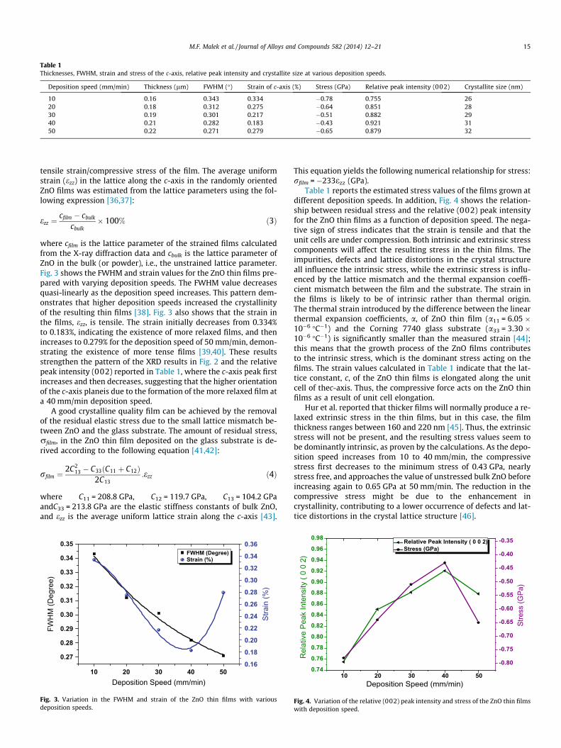
Table 1Thicknesses, FWHM, strain and stress of the c-axis, relative peak intensity and crystallite size at various deposition speeds.
Deposition speed (mm/min) Thickness (lm) FWHM (�) Strain of c-axis (%) Stress (GPa) Relative peak intensity (002) Crystallite size (nm)
10 0.16 0.343 0.334 �0.78 0.755 2620 0.18 0.312 0.275 �0.64 0.851 2830 0.19 0.301 0.217 �0.51 0.882 2940 0.21 0.282 0.183 �0.43 0.921 3150 0.22 0.271 0.279 �0.65 0.879 32
M.F. Malek et al. / Journal of Alloys and Compounds 582 (2014) 12–21 15
tensile strain/compressive stress of the film. The average uniformstrain (ezz) in the lattice along the c-axis in the randomly orientedZnO films was estimated from the lattice parameters using the fol-lowing expression [36,37]:
ezz ¼cfilm � cbulk
cbulk� 100% ð3Þ
where cfilm is the lattice parameter of the strained films calculatedfrom the X-ray diffraction data and cbulk is the lattice parameter ofZnO in the bulk (or powder), i.e., the unstrained lattice parameter.Fig. 3 shows the FWHM and strain values for the ZnO thin films pre-pared with varying deposition speeds. The FWHM value decreasesquasi-linearly as the deposition speed increases. This pattern dem-onstrates that higher deposition speeds increased the crystallinityof the resulting thin films [38]. Fig. 3 also shows that the strain inthe films, ezz, is tensile. The strain initially decreases from 0.334%to 0.183%, indicating the existence of more relaxed films, and thenincreases to 0.279% for the deposition speed of 50 mm/min, demon-strating the existence of more tense films [39,40]. These resultsstrengthen the pattern of the XRD results in Fig. 2 and the relativepeak intensity (002) reported in Table 1, where the c-axis peak firstincreases and then decreases, suggesting that the higher orientationof the c-axis planeis due to the formation of the more relaxed film ata 40 mm/min deposition speed.
A good crystalline quality film can be achieved by the removalof the residual elastic stress due to the small lattice mismatch be-tween ZnO and the glass substrate. The amount of residual stress,rfilm, in the ZnO thin film deposited on the glass substrate is de-rived according to the following equation [41,42]:
rfilm ¼2C2
13 � C33ðC11 þ C12Þ2C13
:ezz ð4Þ
where C11 = 208.8 GPa, C12 = 119.7 GPa, C13 = 104.2 GPaandC33 = 213.8 GPa are the elastic stiffness constants of bulk ZnO,and ezz is the average uniform lattice strain along the c-axis [43].
10 20 30 40 50
0.27
0.28
0.29
0.30
0.31
0.32
0.33
0.34
0.35
Deposition Speed (mm/min)
FWH
M (D
egre
e)
0.16
0.18
0.20
0.22
0.24
0.26
0.28
0.30
0.32
0.34
0.36
Stra
in (%
)
FWHM (Degree)Strain (%)
Fig. 3. Variation in the FWHM and strain of the ZnO thin films with variousdeposition speeds.
This equation yields the following numerical relationship for stress:rfilm = �233ezz (GPa).
Table 1 reports the estimated stress values of the films grown atdifferent deposition speeds. In addition, Fig. 4 shows the relation-ship between residual stress and the relative (002) peak intensityfor the ZnO thin films as a function of deposition speed. The nega-tive sign of stress indicates that the strain is tensile and that theunit cells are under compression. Both intrinsic and extrinsic stresscomponents will affect the resulting stress in the thin films. Theimpurities, defects and lattice distortions in the crystal structureall influence the intrinsic stress, while the extrinsic stress is influ-enced by the lattice mismatch and the thermal expansion coeffi-cient mismatch between the film and the substrate. The strain inthe films is likely to be of intrinsic rather than thermal origin.The thermal strain introduced by the difference between the linearthermal expansion coefficients, a, of ZnO thin film (a11 = 6.05 �10�6 �C�1) and the Corning 7740 glass substrate (a33 = 3.30 �10�6 �C�1) is significantly smaller than the measured strain [44];this means that the growth process of the ZnO films contributesto the intrinsic stress, which is the dominant stress acting on thefilms. The strain values calculated in Table 1 indicate that the lat-tice constant, c, of the ZnO thin films is elongated along the unitcell of thec-axis. Thus, the compressive force acts on the ZnO thinfilms as a result of unit cell elongation.
Hur et al. reported that thicker films will normally produce a re-laxed extrinsic stress in the thin films, but in this case, the filmthickness ranges between 160 and 220 nm [45]. Thus, the extrinsicstress will not be present, and the resulting stress values seem tobe dominantly intrinsic, as proven by the calculations. As the depo-sition speed increases from 10 to 40 mm/min, the compressivestress first decreases to the minimum stress of 0.43 GPa, nearlystress free, and approaches the value of unstressed bulk ZnO beforeincreasing again to 0.65 GPa at 50 mm/min. The reduction in thecompressive stress might be due to the enhancement incrystallinity, contributing to a lower occurrence of defects and lat-tice distortions in the crystal lattice structure [46].
10 20 30 40 500.74
0.76
0.78
0.80
0.82
0.84
0.86
0.88
0.90
0.92
0.94
0.96
0.98 Relative Peak Intensity ( 0 0 2)Stress (GPa)
Deposition Speed (mm/min)
Rel
ativ
e Pe
ak In
tens
ity (
0 0
2)
-0.80
-0.75
-0.70
-0.65
-0.60
-0.55
-0.50
-0.45
-0.40
-0.35
Stre
ss (G
Pa)
Fig. 4. Variation of the relative (002) peak intensity and stress of the ZnO thin filmswith deposition speed.

16 M.F. Malek et al. / Journal of Alloys and Compounds 582 (2014) 12–21
The FESEM morphologies of the ZnO thin films produced at var-ious deposition speeds are shown in Fig. 5 (50 k magnification at5 kV applied voltage). The average grain size determined fromthe micrographs increases as the deposition speed increases from10 mm/min to 50 mm/min. This finding is in agreement with theXRD crystallite size results reported in Table 1. As reported byNumpud et al., the increase in grain size is affected by the deposi-tion speed due to the competitive effects of gravitational and fric-tional viscous forces acting on the liquid coating film and solventevaporation [47]. The coated thin films become thicker as thedeposition speed of the sol–gel process increases. The relationshipbetween the film thickness (t) and the deposition speed (v) is de-fined as t / v2/3 [48]. Therefore, more zinc particles are present inthicker films, increasing the electrostatic interactions between par-ticles. This condition increases the probability that particles con-gregate together to form a grain. Thus, the grain size increases asthe deposition speed is increased. The presence of the nanoparti-cles is more clearly observed in the film morphology for thickerfilms. As the deposition speed of the substrate is increased, no sud-den changes are observed in the surface morphology of the films,with the exception of an increase in particle size. All of the ZnOthin films exhibit uniform coverage of planar grains with irregularshapes, but the porous structure still prevails (Fig. 5a–e). A com-pact and less porous surface covered by larger grains is observedwhen the films are produced at higher deposition speeds.
According to Brinker and Scherer, the thin films become thickeras the deposition speed increases, and the number of Zn2+ particlesin the films increases [22,48]. Thus, the growth rate of the ZnO thinfilms will increase at higher deposition speeds. When the filmgrowth is too fast, there is no chance for the arriving material torearrange into a more definite structure, disturbing the preferredcrystal orientation of the films, as discussed in reference to theXRD results. The voids around the grains are reduced at higherdeposition speeds and increase the efficiency of physical contact,which in turn decreases the resistivity of the films, as previouslyreported. Furthermore, the increase in the particle size in the thinfilm will increase the surface contact between the particles and im-prove the packing density in the thin films. An increase in particlesize at a higher deposition speed can reduce the oxygen adsorptionat the grain boundaries, decreasing carrier trapping in thin films,thus decreasing the resistivity. Carrier traps occur when the ad-sorbed oxygen becomes trapped at the grain boundary, thusincreasing the grain boundary potential barrier among the ZnOparticles. The potential barrier will prevent the carrier from mov-ing from one particle to another, which will decrease the carrier
200 nm
(a) (b)
200 nm
(d) (e
Fig. 5. FESEM morphology of ZnO thin films prepared at various deposition speeds: (a)
mobility of the ZnO thin films prepared at lower deposition speeds.This phenomenon will contribute to an increase in the resistivity ofthe thin film, as discussed in the section above on electrical prop-erties. Nevertheless, the surface contact between ZnO particles canbe improved by increasing the deposition speed, leading to thereduction of oxygen, depriving the carrier traps of charged carriersand thus reducing the resistance by decreasing the potential bar-rier at the grain boundaries [49,50]. Previous reports have notedthat the film thickness increases at higher deposition speeds [48].The film thickness was measured by surface profilometry (KLATencor P-6 profilometer) and was found to be in the range of0.16–0.22 lm. The variation in thickness obtained by the surfaceprofiler is presented in Table 1.
Raman spectroscopy provides information on the vibrationalproperties of ZnO. ZnO with a hexagonal wurtzite structure is wellknown to belong to the space group C4
6V , with two formula unitsper primitive cell. Each unit cell contains 4 atoms and occupies2b sites of symmetry C3V [51]. Group theory predicts that the opti-cal phonons for wurtzite ZnO at the Copt point of the Brillouin zonebelong to the following irreducible representation (5) [52]:
Copt ¼ A1 þ 2B1 þ E1 þ 2E2 ð5Þ
where both the A1 and E1 modes are polar and are split into trans-verse optical modes (A1-TO andE1-TO) resulting from beating in thebasal plane and longitudinal optical modes (A1-LO and E1-LO)resulting from beating along the c-axis, with different frequenciesdue to the macroscopic electric fields associated with LO phonons.For lattice vibrations with A1 and E1 symmetry, the atoms move par-allel and perpendicular to the c-axis, respectively. The A1 and E1
branches are both Raman and infrared active. The two non-polarE2 modes are Raman active only. Only B1 modes are inactive (silentmodes). In the case of highly oriented ZnO films, the incident lightwas exactly normal to the surface; only the E2 modes and the A1-LOmode were expected to emerge, and the other modes were forbid-den according to the well-known Raman selection rules [51]. Fig. 6apresents typical Raman spectra of the ZnO films deposited at vari-ous deposition speeds. The observed phonon frequencies are E2
(low) = �101 cm�1, E2 (high) = �437 cm�1, and A1-LO = �585 cm�1.These optical phonon modes confirm that these nanocrystallinefilms contain the wurtzite hexagonal phase.
Some researchers have reported that the E2 (low) peak candetermine the crystallinity of the films and is associated with thevibration of the heavy Zn sublattice [53]. If the E2 (low) peak isthe sharpest and highest intensity peak, then the sample has thebest crystal quality. The E2 (high) mode of ZnO is often related to
200 nm 200 nm
(c)
200 nm
)
10 mm/min, (b) 20 mm/min, (c) 30 mm/min, (d) 40 mm/min and (e) 50 mm/min.

100 150 200 250 300 350 400 450 500 550 600 650 700 750 800
437 cm-1A1-LOE2 (high)E2 (low)
10 mm/min
50 mm/min
40 mm/min
30 mm/min
Ram
an In
tens
ity (a
rb. u
nits
)
Wavenumbers (cm-1) Wavenumbers (cm-1)
20 mm/min
(a)
350 400 450 500 550
437 cm-1 E2 (high)
10 mm/min
50 mm/min
40 mm/min
30 mm/min
Ram
an In
tens
ity (a
rb. u
nits
)
20 mm/min
(b)
Fig. 6. (a) Raman spectra of ZnO thin films prepared at various deposition speeds and (b) an enlarged view of the signal ranging from 350 to 550 cm�1.
M.F. Malek et al. / Journal of Alloys and Compounds 582 (2014) 12–21 17
oxygen atoms, and it is shifted due to the intrinsic stress in ZnOfilms. According to the Raman results, the E2 (high) peak shift tohigher wavenumbers compared with the bulk value of 437 cm�1
indicates the existence of a compressive stress in the films, whichwas confirmed by XRD results [54]. The peak shift can be clearlyobserved in Fig. 6b, which is indicative of the trend of compressivestress in the ZnO films.
The peak of the A1-LO mode of ZnO is associated with oxygendeficiency. Some reports assigned this wavenumber as E1-LO[55]. A1-LO has often been associated with the wavenumbers of570 cm�1, 574 cm�1, 579 cm�1 and 582 cm�1 [56]. According tothe theoretical calculation, the A1-LO theoretical wavenumber is559 cm�1. A higher wavenumber contribution suggests animprovement in the crystallinity and a reduction in the defects ofthe ZnO films [57]. TheA1-LO mode exhibited a very weak intensity,indicating the minimisation of the effect of oxygen deficiency onthe growth of strongly c-axis-oriented ZnO films. The preparationof ZnO films with a strong c-axis orientation will enhance the elec-tron transport in the vertical direction, which is important for lightharvesting applications for high performance optical devices suchas light emitting diodes (LEDs) and solar cells [58].
3.2. Optical properties
Fig. 7 presents the transmittance spectra of as-grown films inthe wavelength range of 300–1500 nm. All ZnO thin filmsexhibited a high transparency of over 85% in the visible and NIR re-gions, while the absorption edges were below 400 nm for all ZnO
300 450 600 750 900 1050 1200 1350 15000
10
20
30
40
50
60
70
80
90
100
(a) 10 mm/min
(b) 20 mm/min
(c) 30 mm/min
(d) 40 mm/min
(e) 50 mm/min
Tran
smitt
ance
(%)
Wavelength (nm)
(a)
(b) (e)(d)(c)
Fig. 7. Transmittance spectra of ZnO thin films prepared at various depositionspeeds as a function of wavelength.
thin films. This finding was attributed to the intrinsic band gapof the ZnO due to electron transitions from the valence band tothe conduction band.
The transmission decreased sharply near the ultraviolet regionat approximately 380 nm, corresponding to the intrinsic bandgap energy of ZnO. The deposition speed had little influence onthe pattern of the transmittance spectra. However, the averagetransmittance in the visible range proved that a higher transmit-tance (over 90%) is achieved at a lower deposition speed, as shownin Table 2. The lower average transmittance properties of the ZnOthin films prepared at higher deposition speeds may be due to theincreases in particle size and film thickness and the presence ofvoids around the grains, as previously discussed in reference tothe FESEM results. At higher deposition speeds (>10 mm/min),the ZnO thin films exhibited a decrease in the optical transmittancedue to the formation of larger particles, which may have increasedthe optical scattering at the grain boundaries. The increase in thefilm thickness at higher deposition speeds also increased the opti-cal scattering, reducing the transmittance of the thin films. Theabsorption coefficient, a, can be calculated using Lambert’s Lawbased on relation (6):
a ¼ 1t
ln1T
� �ð6Þ
where t is the thickness of the thin film and T is the transmittance ofthe thin film. The absorption coefficients of 0.4 M ZnO thin filmsproduced at various deposition speeds are presented in Fig. 8. Thespectra reveal an increase in the absorption coefficient in the UV re-gion (<400 nm) as the deposition speed is increased to 40 mm/min.Moreover, the absorption coefficient demonstrates an excitonic nat-ure that becomes more prominent as the deposition speed in-creases. This effect is attributed to the pattern of strain withincreasing deposition speed. The reduction of UV light absorptionfor the ZnO thin films prepared at a 50 mm/min deposition speedmight be due to the formation of higher order defects in the thin
Table 2Optical properties and porosity of ZnO thin films prepared at various depositionspeeds.
Depositionspeed (mm/min)
Averagetransmittance(%)
Opticalbandgapenergy (eV)
Urbachenergy(meV)
Porosity(%)
10 93.99 3.276 86 49.7020 93.87 3.280 63 49.0030 91.56 3.283 61 38.1040 91.47 3.289 60 37.7650 91.45 3.286 63 37.68

400 500 600 700 800 900 1000 1100 1200 1300 1400 15000.00.20.40.60.81.01.21.41.61.82.02.2
(a) 10 mm/min(b) 20 mm/min(c) 30 mm/min(d) 40 mm/min(e) 50 mm/min
Wavelength (nm)
Abso
rptio
n C
oeffi
cien
t,α
(x10
7 m-1)
(d)
(e)(c)(b)
(a)
Fig. 8. Absorption coefficient, a, of ZnO thin films prepared at various depositionspeeds as a function of wavelength.
3.0 3.1 3.2 3.3 3.4 3.50.0
1.0
2.0
3.0
4.0
5.0
( αhv
)2(×
1015 e
V2 m
-2)
(e)
(b)
(c)
(a)
(a) 10 mm/min(b) 20 mm/min(c) 30 mm/min(d) 40 mm/min(e) 50 mm/min
Photon Energy (eV)
(d)
Fig. 9. Estimates of the optical band gap energy, Eg, of ZnO thin films using Tauc’splot as a function of deposition speed.
10 20 30 40 503.274
3.276
3.278
3.280
3.282
3.284
3.286
3.288
3.290
Stre
ss (G
Pa)
Bandgap Energy (eV) Stress (GPa)
Deposition Speed
Band
gap
Ener
gy (e
V)
0.40
0.45
0.50
0.55
0.60
0.65
0.70
0.75
0.80
Fig. 10. Variation of the optical band gap energy, Eg, and compressive stress of ZnOthin films as a function of deposition speed.
18 M.F. Malek et al. / Journal of Alloys and Compounds 582 (2014) 12–21
films as the preferred growth orientation along the c-axis plane de-creases [12]. Meanwhile, the absorption coefficient in the visible re-gion (400–800 nm) does not exhibit any significant change with thedeposition speed. However, the highest absorption coefficient wasobserved for the film deposited at 40 mm/min. This result fits withthe improvement in the film crystallinity along the preferred c-axisplane, which enhanced the light absorption at the grain boundaries[19]. The optical band gap energy (Eg) values of the films weredetermined by applying the Tauc model in the high absorption re-gion using the following relations [59,60]:
ahv ¼ Bðhv � EgÞn ð7Þ
ahv ¼ Bffiffiffiffiffiffiffiffiffiffiffiffiffiffiffiffiffihv � Eg
qð8Þ
where a is the absorption coefficient, hv is the photon energy, Eg isthe optical band gap and B is an energy-independent constant withvalues between 1 � 105 and 1 � 106 cm�1 eV�1 [60,61]. For n = 1/2,the transition data provide the best linear curve in the band edgeregion, implying that the transition is direct in nature. The absorp-tion coefficient, a, must be assumed to satisfy the equation for aband gap direct material to calculate the band gap energy of thefilms, as shown in Eq. (7). The optical band gap values, Eg, of theZnO films were obtained from the transmission measurements byplotting (ahm)2 versus hm and extrapolating the linear portion ofthe absorption edge to find the intercept with the energy axis. Sharpultraviolet absorption edges at approximately k = 380 nm can beobserved, with the absorption edge shifted to shorter wavelengthsas the deposition speed is increased to 40 mm/min. However, theband edge is shifted to a longer wavelength at a deposition speedof 50 mm/min. The shift in the band edge can be clearly observedin Fig. 9. From the Tauc plot, the estimated optical band gap energyof the ZnO thin films ranged between 3.276 and 3.289 eV, which isin close agreement with the values reported by other researchersfor polycrystalline ZnO thin films and with published values forZnO electronic transition band gap data [62]. The variation in theoptical band gap might be due to the optical scattering by grainboundaries and aggregates, which are influenced by the variousdeposition speeds. The variations in compressive stress and bandgap energy, Eg, with deposition speed are shown in Fig. 10. The bandgap energy value, Eg, is consistent with the trend in the stress. Thestress changes the interatomic spacing of semiconductors, which af-fects the energy gap [63]. The band gap energy, Eg, increases withincreasing tensile stress along the c-axis but decreases with increas-ing compressive stress [37,64]. The compressive stress in the filmsleads to a decrease in the band gap. The compressed lattice is ex-pected to provide a narrower band gap because of the decreased
repulsion between the zinc 4s and oxygen 2p bands [37], thusexplaining the increase in Eg with the decrease in compressivestress as the deposition speed increases.
The absorption coefficient near the fundamental absorptionedge exhibits an exponential dependence on the incident photonenergy and obeys the empirical Urbach relation. The absorptionedge in the spectral range of direct optical transitions has an expo-nential shape described by the following equation [65]:
a ¼ ao exphvEu
� �ð9Þ
where ao is the pre-exponential factor and Eu is known as the Ur-bach energy, which is the width of the localised state. Taking thenatural logarithm of Eq. (9) yields the following equation:
lna ¼ lnao þhvEu
� �ð10Þ
Thus, a plot of ln(a) versus photon energy, hm, should be linear,with the slope representing the Urbach energy. Fig. 11 presents theUrbach plots of the films. The Urbach energy was calculated fromthe reciprocal gradient of the linear portion of these curves andis interpreted in Fig. 12. Urbach energy values, Eu, vary inverselywith the optical band gap energy, Eg. The Urbach energy first grad-ually decreases and then increases for deposition speeds exceeding40 mm/min, thus indicating defect formation. During the forma-tion of these films, some defects are formed that produce localisedstates in the films. Thus, the increase in the width of the localisedstates (Urbach energy) decreases the optical band gap energy

10 20 30 40 5055
60
65
70
75
80
85
90
Urb
ach
Energ
y(m
eV
)
Deposition Speed (mm/min)
Fig. 12. Urbach energy, Eu, of ZnO thin films as a function of deposition speed.
350 400 450 500 550 600 650 700
Inte
nsity
(arb
. uni
ts)
(e)(d)
(c)(b)
(a) 10mm/min(b) 20mm/min(c) 30mm/min(d) 40mm/min(e) 50mm/min
Wavelength (nm)
(a)
Fig. 13. Photoluminescence spectra of the ZnO thin films as a function of depositionspeed.
M.F. Malek et al. / Journal of Alloys and Compounds 582 (2014) 12–21 19
[66,67]. This effect explains the changes in the c-axis orientationpattern as the deposition speed is increased. The porosity of theZnO thin films has been calculated using the Lorentz–Lorentzequation presented below [21,68]:
Porosity ¼1�½ðn2
f � 1Þ=ðn2f þ 2Þ�
½ðn2s � 1Þ=ðn2
s þ 2Þ�
" #ð11Þ
where nf is the refractive index of the porous ZnO film and ns is therefractive index of the ZnO skeleton, which is widely accepted as 2[69]. In the transmittance region where the absorption coefficienta = 0, the refractive index, nf, is calculated based on the followingequations [70]:
nf ¼ N þ ðN2 � s2Þ1=2h i1=2ð12Þ
N ¼ 2sTm� ðs2 þ 1Þ
2
� �ð13Þ
Tm is the envelope function of the transmittance maxima and min-ima, while s is the refractive index of the substrate, which is typi-cally 1.52 for the totally transparent glass substrate used in thisstudy [71]. The Tm value is obtained by taking the average of thetransmittance data from the transparent region, or the region wherethe a value is close to 0 [39]. Based on the results of this study, thisregion is between wavelengths of 400 and 800 nm. The porositiescalculated for all films are summarised in Table 2. The results inthe table suggest that the porosity tends to decrease at higher depo-sition speeds.
3.3. Photoluminescence
Fig. 13 presents the PL spectra of the ZnO thin films prepared atvarious deposition speeds. The luminescence of the ZnO thin filmsis closely related to the film crystallinity because the density of de-fects in the film decreases as the crystallinity is improved. Roomtemperature PL emission spectra for all of the films were measuredin the wavelength range of 350–700 nm at an excitation wave-length of 325 nm. Generally, ZnO films exhibit two emission peaks,the UV emission and the deep-level emission in the visible range.The PL spectra in all samples exhibit a strong UV emission at thenear band edge centred at 380 nm due to free-exciton recombina-tion [72,73]. The UV peak increases with the deposition speed. Theintensity increases with increasing deposition speed because thethicker film contains more zinc particles, leading to an increasein the carrier concentration and enhancing the UV emission [74].A broad visible emission ranging from 520 to 640 nm with a peaklocated in the yellow range (610 nm) was observed for the deep-le-
2.9 3.0 3.1 3.2 3.3 3.4 3.512
13
14
15
16
17
(a) 10 mm/min(b) 20 mm/min(c) 30 mm/min(d) 40 mm/min(e) 50 mm/min
Photon Energy (eV)
ln( α
)
(a) (b)
(e)(d)
(c)
Fig. 11. Plot of ln(a) versus photon energy for ZnO thin films prepared at variousdeposition speeds.
vel emission in the ZnO thin films and was attributed to structuraldefects such as oxygen vacancies (Vþo ) and interstitial oxygen (O�i )[75,76]. Biaxial strain in ZnO films only affects UV emission anddoes not change the position or intensity of deep level emission.
3.4. Electrical properties
The deposition speed might play an important role in the sheetresistivity of thin films. Therefore, an I–V characteristic curve of thefilms prepared at various speeds is plotted in Fig. 14. The resistivitywas calculated from the slopes of the linear I–V plot using the sheetresistivity formula (14) for a thin film:
q ¼ VI
� �wtl
ð14Þ
where V is the supplied voltage, I is the measured current, t is thefilm’s thickness, w is the electrode width and l is the length betweenthe electrodes. The conductivity of the film, r, was determinedusing the following equation :
r ¼ 1q
ð15Þ
The active area of the thin films is 3 � 10�6 m2. The inset in Fig. 14shows the variation in resistivity with respect to deposition speed.The I–V results show that all of the films exhibit ohmic behaviour.The resistivity decreases with increasing deposition speed, andthe minimum resistivity was observed for the films deposited at50 mm/min, while the maximum resistivity was observed for thefilms prepared at a 10 mm/min deposition speed. A higher deposi-

-10 -8 -6 -4 -2 0 2 4 6 8 10-1.0
-0.8
-0.6
-0.4
-0.2
0.0
0.2
0.4
0.6
0.8
1.0-10 -8 -6 -4 -2 0 2 4 6 8 10
-1.0
-0.8
-0.6
-0.4
-0.2
0.0
0.2
0.4
0.6
0.8
1.0
10 20 30 40 50
6.8
7.0
7.2
7.4
7.6
7.8
Deposition Speed (mm/min)
Res
istiv
ity (1
×102
Ω.c
m)
10 mm/min
20 mm/min
30 mm/min
40 mm/min
50 mm/min
Cur
rent
(µA)
Voltage (V)
Fig. 14. I–V characteristic curves of the ZnO thin films prepared at variousdeposition speeds. The inset shows the variation in resistivity as a function ofdeposition speed.
0.20.4
0.60.8
1.0
0.0
0.2
0.4
0.6
0.8
1.0
1020
3040
50Pref
erre
d c -
axi
s or
ient
atio
n
Sol Concentration (M)
Depos
ition S
peed
(mm/m
in)
Fig. 15. Response surface/contour diagrams as a function of sol concentration anddeposition speed.
20 M.F. Malek et al. / Journal of Alloys and Compounds 582 (2014) 12–21
tion speed will produce a thicker thin film due to the competitiveeffects of gravitational and frictional viscous forces acting on the li-quid film coating and solvent evaporation [21,23,77]. This evapora-tion process between the deposition processes increases the solviscosity, which in turn results in a thicker film [78]. The I–V trendsuggests that the Zn2+ species is present at higher levels in thickerthin films due to the higher deposition speed, which enhances thecarrier concentration in thin films [24]. The patterns of resistivityand conductivity are summarised in Table 3.
4. Response surface/contour
Based on our previous paper on sol concentration [19] and thepresent research on deposition speed, a response surface plotwas prepared considering the relative peak intensity as the re-sponse. Fig. 15 presents the plot as a function of sol concentrationand deposition speed, which enables the optimisation of the prep-aration of c-axis oriented ZnO thin films. The results suggest thatthe deposition speed has no clear effect on the orientation of thegrain growth. Indeed, the XRD analysis shows that the grains werealways oriented according to the c-axis perpendicular to the sub-strate surface, regardless of the deposition speed. The orientedgrain growth of the (002) plane may occur because of the presenceof slightly oriented grains in the previous layer. However, variousdiffraction peaks were observed for every sol concentration. Athigher sol concentrations, the (002) peak decreased with increas-ing Zn concentration, while the (100), (101), (102) and (110)peaks gradually increased, indicating an increase in the grainboundary density for the thin films. However, the crystallite sizewas influenced by both parameters, with increases in both param-eters leading to increases in the crystallite size. This study of the
Table 3Electrical properties and thicknesses of ZnO thin films prepared at various depositionspeeds.
Precursorconcentration (M)
Deposition speed(mm/min)
Resistivity, q(O cm)
Conductivity, r(S cm�1)
0.4 10 7.86 � 102 1.27 � 10�3
20 7.51 � 102 1.33 � 10�3
30 7.14 � 102 1.40 � 10�3
40 7.10 � 102 1.41 � 10�3
50 6.84 � 102 1.46 � 10�3
effects of sol concentration and deposition speed demonstratesthat the ZnO thin film prepared at 0.4 M and deposited at40 mm/min exhibited the highest crystal orientation along thec-axis plane.
5. Conclusions
A ZnO film with a highly preferred c-axis (002) orientation wasobtained at a deposition speed of 40 mm/min by the sonicated sol–gel dip-coating technique. The existence of only one texture in allcases, namely, the c-axis texture, shows that the growth orienta-tion of these films is independent of the deposition speed. Thecrystalline quality of the films improved at 40 mm/min, and corre-sponding increases in crystallite and grain growth were observedas the deposition speed was increased. Increasing the depositionspeed also minimised the strain and stress in the film, which en-hanced the electron transport and increased the conductivity dueto the shorter carrier pathway. The films deposited at a low depo-sition speed (10 mm/min) had a large stress (0.78 GPa), which re-laxed as the deposition speed was increased. Meanwhile, a nearlystress- and strain-free thin film was obtained for ZnO thin filmsdeposited at 40 mm/min. In addition, the variation of the directband gap, Eg, was correlated with the compressive stress of ZnOthin films. All of the films exhibited greater than 90% transmittancein the visible region. Furthermore, the electrical resistivity wasfound to decrease with deposition speed, while the carrier concen-tration increased with deposition speed, as proven by the PL emis-sion. These results suggest that a suitable deposition speed shouldbe used to obtain higher crystalline and stress-free ZnO thin filmsfor applications in optoelectronic devices such as sensors and solarcells.
Acknowledgements
Mohd Firdaus Malek would like to thank the Research Manage-ment Institute (RMI), Universiti Teknologi MARA (UiTM), Malaysiaand the Ministry of Higher Education (MOHE), Malaysia for theirfinancial support. The authors would also like to thank the Facultyof Applied Sciences (UiTM) and the Faculty of Mechanical Engi-neering (UTHM) for the use of their FESEM and XRD facilities,respectively. The authors thank Mrs. Nurul Wahida (UiTM Asst.Science Officer), Mr. Mohd Azlan Jaafar (UiTM technician) and

M.F. Malek et al. / Journal of Alloys and Compounds 582 (2014) 12–21 21
Mr. Suhaimi Ahmad (UiTM technician) for their kind support ofthis research.
References
[1] H. Wu, M. Xue, J. Ou, F. Wang, W. Li, J. Alloys Comp. 565 (2013) 85.[2] H. Li, Z. Zhang, J. Huang, R. Liu, Q. Wang, J. Alloys Comp. 550 (2013) 526.[3] C. Klingshirm, Phys. Status Solidi B 71 (1975) 547.[4] J.Y. Lee, J.H. Lee, H.S. Kim, C.H. Lee, H.S. Ahn, H.K. Cho, Y.Y. Kim, B.H. Kong, H.S.
Lee, Thin Solid Films 517 (2009) 5157.[5] J.J. Hassan, M.A. Mahdi, Y. Yusof, H. Abu-Hassan, Z. Hassan, H.A. Al-Attar, A.P.
Monkman, Opt. Mater. 35 (2013) 1035.[6] A.M.K. Dagamseh, B. Vet, F.D. Tichelaar, P. Sutta, M. Zeman, Thin Solid Films
516 (2008) 7844.[7] C.S. Rout, A.R. Raju, A. Govindaraj, C.N.R. Rao, Solid State Commun. 138 (2006)
136.[8] A. Fouchet, W. Prellier, B. Mercey, J. Appl. Phys. 100 (2006) 013901.[9] Z. Charifi, H. Baaziz, A.H. Reshak, Phys. Status Solidi B 244 (2007) 3154.
[10] D. Bao, H. Gu, A. Kuang, Thin Solid Films 312 (1998) 37.[11] A.M.P. Santos, Edval J.P. Santos, Thin Solid Films 516 (2008) 6210.[12] S. Suwanboon, Naresuan Univ. J. 6 (2008) 173.[13] M. Bouderbala, S. Hamzaoui, B. Amrani, Ali H. Reshak, M. Adnane, B. Amrani, T.
Sahraoui, M. Zerdali, Physica B 403 (2008) 3326.[14] K. Ozga, T. Kawaharamura, A.A. Umar, M. Oyama, K. Nouneh, A. Slezak, S.
Fujita, M. Piasecki, A.H. Reshak, I.V. Kityk, Nanotechnology 19 (2008) 185709.[15] A.H. Reshak, J. Ebothe, A. Wojciechowski, W. Kuznik, A. Popeda, Physica E 42
(2010) 1769.[16] R. Shabannia, H.A. Hassan, Mater. Lett. 98 (2013) 135.[17] S. Salam, M. Islam, A. Akram, Thin Solid Films 529 (2013) 242.[18] Q.A. Drmosh, S.G. Rao, Z.H. Yamani, M.A. Gondal, Appl. Surf. Sci. 270 (2013)
104.[19] M.F. Malek, M.H. Mamat, M.Z. Sahdan, M.Z. Musa, Z. Khusaimi, M. Rusop, Thin
Solid Films 527 (2013) 102.[20] M.F. Malek, M.Z. Sahdan, M.H. Mamat, M.Z. Musa, Z. Khusaimi, S.S. Husairi,
N.D. Md Sin, M. Rusop, Appl. Surf. Sci. 275 (2013) 75.[21] C.J. Brinker, G.W. Scherer, Sol–Gel Science: The Physics and Chemistry of Sol–
Gel Processing, Academic Press, New York, 1975. 803.[22] W.R. Saleh, N.M. Saeed, W.A. Twej, M. Alwan, Adv. Mater. Phys. Chem. 2 (2012)
11.[23] M. Ohyama, H. Kouzuka, T. Yoko, Thin Solid Films 306 (1997) 78.[24] D.J. Goyal, C.M. Agashe, B.R. Marathe, M.G. Takwale, V.G. Bhide, J. Mater. Sci.
Lett. 11 (1992) 708.[25] O. Kozák, P. Praus, R. Dvorsk, Chalcogenide Lett. 9 (2012) 413.[26] M.H. Mamat, Z. Khusaimi, M.M. Zahidi, S.A. Bakar, Y.M. Siran, S.A.M. Rejab, A.J.
Asis, S. Tahiruddin, S. Abdullah, M.R. Mahmood, Jpn. J. Appl. Phys. 50 (2011)06GH04.
[27] S. O’Brien, L.H.K. Koh, Gabriel M. Crean, Thin Solid Films 516 (2008) 1391.[28] V.R. Shinde, T.P. Gujar, C.D. Lokhande, Sens. Actuat., B 120 (2007) 551.[29] M.J. Alam, D.C. Cameron, J. Vac. Sci. Technol., A 19 (2001) 1642.[30] Y. Zhang, H. Zheng, J. Su, B. Lin, Z. Fu, J. Lumin. 124 (2007) 252.[31] N. Fujimara, T. Nishibara, S. Goto, J. Xu, T. Ito, J. Cryst. Growth 130 (1993) 269.[32] Xu Linhua, Xiangyin Li, Jun Yuan, J. Nonlinear Opt. Phys. Mater. 17 (2008) 405.[33] B.D. Cullity, Elements of X-Ray Diffraction, Addison-Wesley Publishing
Company, Inc., London, 1978.[34] M.Z. Sahdan, M.H. Mamat, M. Salina, Z. Khusaimi, U.M. Noor, M. Rusop, Phys.
Status Solidi C 7 (2010) 2286.[35] E.F. Keskenler, M. Tomakin, S. Dogan, G. Turgut, S. Aydın, S. Duman, B.
Gürbulak, J. Alloys Comp. 550 (2013) 129.[36] Selected powder diffraction data for metals and alloys, JCPDS, USA 1, 1978,
108.[37] R. Ghosh, D. Basak, S. Fujihara, J. Appl. Phys. 96 (2004) 2689.
[38] J.M. Myong, W.H. Yoon, D.H. Lee, I. Yun, S.H. Bae, S.Y. Lee, Jpn. J. Appl. Phys. 41(2002) 28.
[39] S. Mridha, D. Basak, Mater. Res. Bull. 42 (2007) 875.[40] B.L. Zhu, X.H. Sun, S.S. Guo, X.Z. Zhao, J. Wu, R. Wu, J. Liu, Jpn. J. Appl. Phys. 45
(2006) 7860.[41] V. Gupta, A. Mansingh, J. Appl. Phys. 80 (1996) 1063.[42] X.J. Ping, S.S. Bo, L. Lan, Z.X. Song, W.Y. Xin, C.X. Ming, Chin. Phys. Lett. 27
(2010) 047803.[43] Y.G. Wang, S.P. Lau, H.W. Lee, S.F. Yu, B.K. Tay, X.H. Zhang, K.Y. Tse, H.H. Hng, J.
Appl. Phys. 94 (2003) 1597.[44] J.H. Jou, M.Y. Han, D.J. Cheng, J. Appl. Phys. 71 (1992) 4333.[45] T.B. Hur, Y.H. Hwang, H.K. Kim, I.J. Lee, J. Appl. Phys. 99 (2006) 064308.[46] S.Y. Kuo, W.C. Chen, F.I. Lai, C.P. Cheng, H.C. Kuo, S.C. Wang, W.F. Hsieh, J. Cryst.
Growth 287 (2006) 78.[47] P. Numpud, T. Charinpanitkul, W. Tanthapanichakoon, J. Ceram. Soc. Jpn. 116
(2008) 414.[48] C.J. Brinker, G.W. Scherer, Sol–Gel Science: The Physics and Chemistry of Sol–
Gel Processing, Academic Press, San Diego, Calif, USA, 1990. 788.[49] M. Boshta, F.A. Mahmoud, M.H. Sayed, J. Avonic Res. 6 (2010) 93.[50] K. Ogata, K. Sakurai, Sz. Fujita, Sg. Fujita, K. Matsushige, J. Cryst. Growth 214
(2000) 312.[51] T.C. Damen, S.P.S. Porto, B. Tell, Phys. Rev. B 142 (1966) 570.[52] C.A. Arguello, D.L. Rousseau, S.P. Porto, Phys. Rev. 181 (1969) 1351.[53] J.N. Zeng, J.K. Low, Z.M. Ren, T. Liew, Y.F. Lu, Appl. Surf. Sci. 197–198 (2002)
362.[54] C. Wang, Z. Chen, Y. He, L. Li, D. Zhang, Mater. Sci.-Poland 28 (2010) 153.[55] X.L. Xu, S.P. Lau, B.K. Tay, Thin Solid Films 398–399 (2001) 244.[56] J. Ye, S. Gu, S. Zhu, T. Chen, W. Liu, F. Qin, L. Hu, R. Zhang, Y. Shi, Y. Zheng, J. Vac.
Sci. Technol., A 21 (2003) 979.[57] C. Charpentier, P. Prod’homme, I. Maurin, M. Chaigneau, P. Roca i Cabarrocas,
EPJ Photovoltaics 2 (2011) 25002.[58] W.E. Buhro, V.L. Colvin, Nat. Mater. 2 (2003) 138.[59] J. Tauc, R. Grigorovici, A. Vancu, Phys. Status Solid 15 (1996) 627.[60] E.A. Davis, N.F. Motta, Philos. Mag. 22 (1970) 903.[61] S.A.B.S.A. Bux, S.H.A. Aziz, Z.A. Talib, W.M.D.W. Yusoff, Solid State Sci. Technol.
13 (2005) 251.[62] J. Rodríguez-Báez, A. Maldonado, G. Torres-Delgado, R. Castanedo-Pérez, M. de
la L. Olvera, Mater. Lett. 60 (2006) 1594.[63] J.I. Pankove, Optical Processes in Semiconductors, Dover Publication, New
York, 1971. 22.[64] V. Srikant, D.R. Clarke, J. Appl. Phys. 81 (1997) 6357.[65] S. Ilican, M. Caglar, Y. Caglar, J. Optoelectron. Adv. Mater. 9 (2007) 1414.[66] C.I. Oriaku, J.C. Osuwa, C.H. Njoku, J. Non-Oxide Glasses 3 (2011) 25.[67] A. Meeder, D. Fuertes MarrÓn, A. Rumberg, M.Ch. Lux-Steiner, J. Appl. Phys. 92
(2002) 3016.[68] J.H. Yim, J.B. Kim, H.D. Jeong, Y.Y. Lyu, S.K. Mah, J.H. Lee, K.H. Lee, S. Chang, L.S.
Pu, Y.F. Hu, J.N. Sun, D.W. Gidley, Mater. Res. Soc. Symp. Proc. 766 (2003)E8.10.1.
[69] G. Wypych, Handbook of Fillers, second ed., Chem Tech. Publishing, Canada,1999. pp. 172.
[70] V. Pandey, N. Mehta, S.K. Tripathi, A. Kumar, J. Optoelectron. Adv. Mater. 7(2005) 2641.
[71] R. Tricker, Optoelectronics and Fiber Optic Technology, Newnes, Woburn,2002. pp. 39.
[72] J.C. Johnson, H. Yan, P. Yang, R.J. Saykally, J. Phys. Chem. B 107 (2003) 8816.[73] L.E. Greene, M. Law, J. Goldberger, F. Kim, J.C. Johnson, Y. Zhang, R.J. Saykally, P.
Yang, Angewandte Chemie 115 (2003) 3139.[74] C.J. Brinker, G.C. Frye, A.J. Hurd, C.S. Ashley, Thin Solid Films 201 (1991) 97.[75] X.L. Wu, G.G. Siu, C.L. Fu, H.C. Ong, Appl. Phys. Lett. 78 (2001) 2285.[76] K. Vanheusden, W.L. Warren, C.H. Seager, D.R. Tallant, J.A. Voigt, B.E. Gnade, J.
Appl. Phys. 79 (1996) 7983.[77] P. Yimsiri, M.R. Mackley, Chem. Eng. Sci. 61 (2006) 3496.[78] L. Landau, B. Levich, Acta Physicochim., URSS 17 (1942) 42.