Embed Size (px)
Citation preview
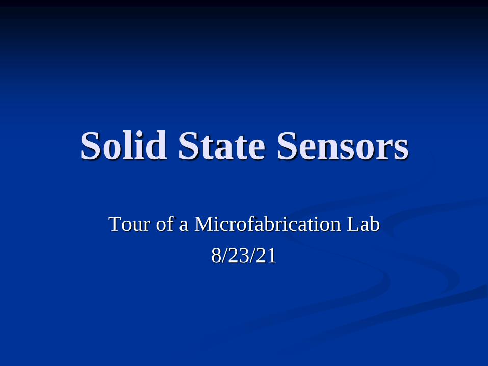
Solid State Sensors
Tour of a Microfabrication Lab
8/23/21
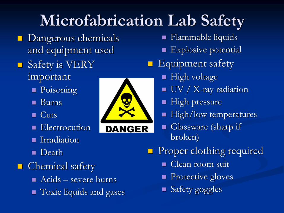
Microfabrication Lab Safety Dangerous chemicals
and equipment used
Safety is VERY important
Poisoning
Burns
Cuts
Electrocution
Irradiation
Death
Chemical safety
Acids – severe burns
Toxic liquids and gases
Flammable liquids
Explosive potential
Equipment safety
High voltage
UV / X-ray radiation
High pressure
High/low temperatures
Glassware (sharp if broken)
Proper clothing required
Clean room suit
Protective gloves
Safety goggles

A Microlab when Safety is
Ignored
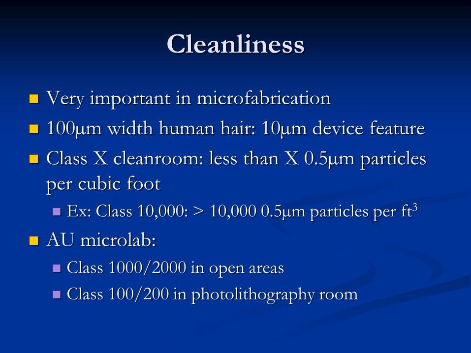
Cleanliness
Very important in microfabrication
100µm width human hair: 10µm device feature
Class X cleanroom: less than X 0.5µm particles
per cubic foot
Ex: Class 10,000: > 10,000 0.5µm particles per ft3
AU microlab:
Class 1000/2000 in open areas
Class 100/200 in photolithography room
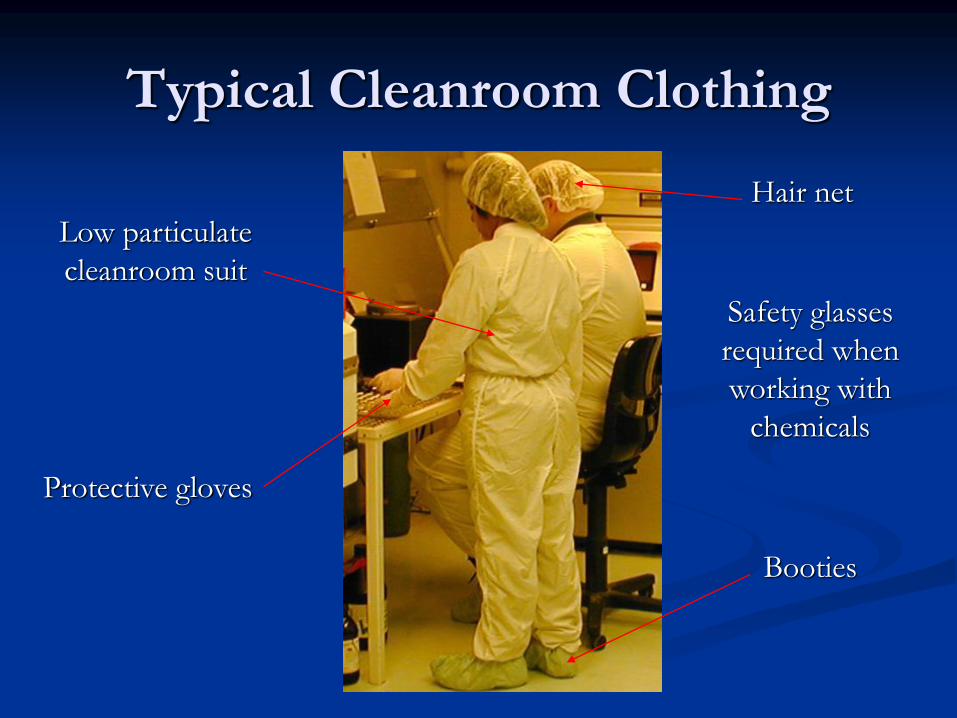
Typical Cleanroom Clothing
Low particulate
cleanroom suit
Protective gloves
Hair net
Booties
Safety glasses
required when
working with
chemicals

Oxidation and Diffusion Furnace
For thermally growing Silicon Dioxide (SiO2) on Si wafers
Uses an oxygen torch and a hydrogen torch
Oxidation process
For diffusion doping of Si wafers
To make n-type or p-type regions
Such as piezoresistors
Oxidation and Diffusion Furnace
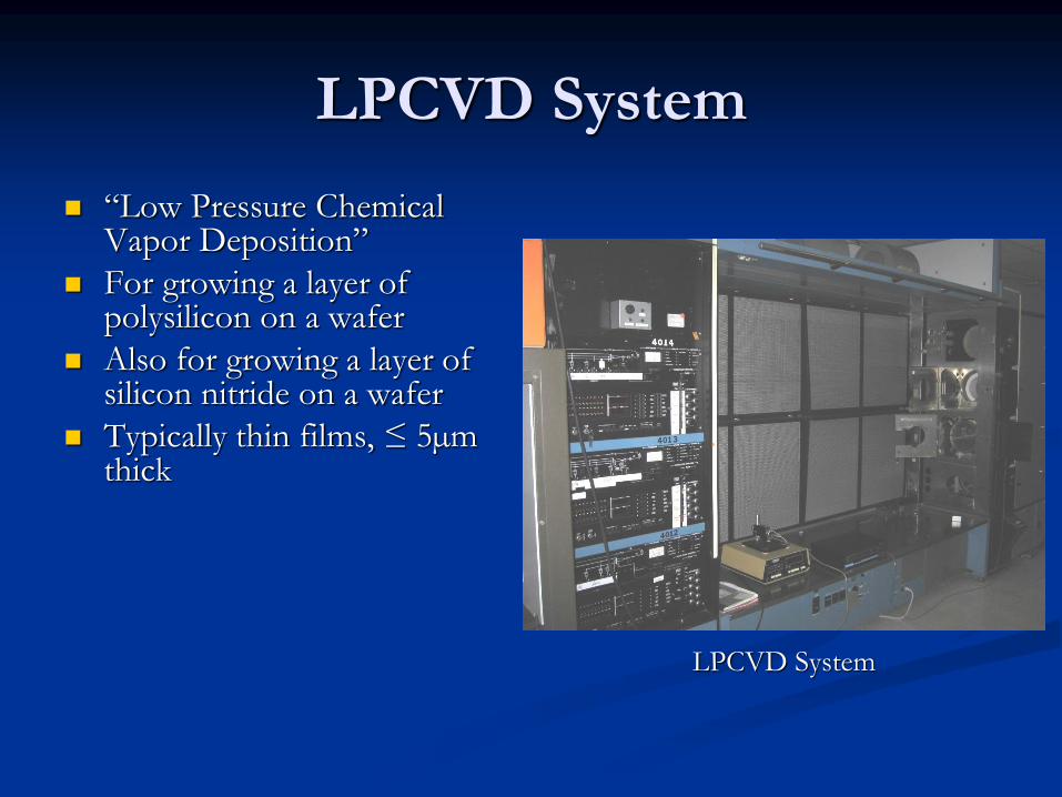
LPCVD System
“Low Pressure Chemical Vapor Deposition”
For growing a layer of polysilicon on a wafer
Also for growing a layer of silicon nitride on a wafer
Typically thin films, ≤ 5µm thick
LPCVD System
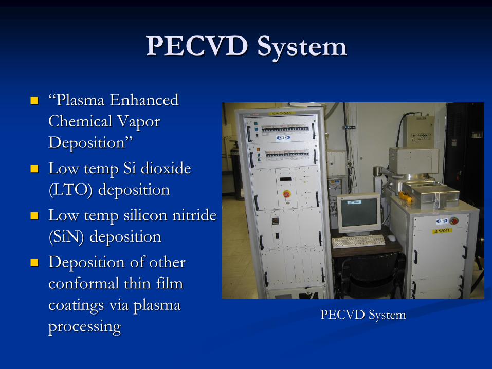
PECVD System
“Plasma Enhanced
Chemical Vapor
Deposition”
Low temp Si dioxide
(LTO) deposition
Low temp silicon nitride
(SiN) deposition
Deposition of other
conformal thin film
coatings via plasma
processingPECVD System
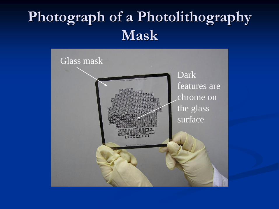
Photograph of a Photolithography
Mask
Glass mask
Dark
features are
chrome on
the glass
surface
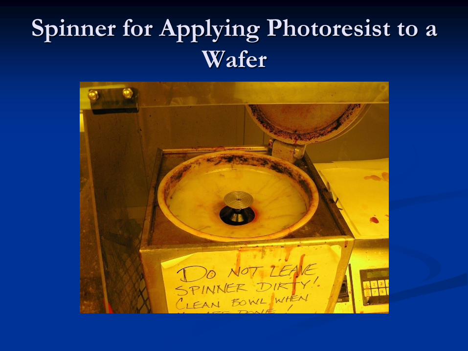
Spinner for Applying Photoresist to a
Wafer

Photograph of a MA/BA6 Mask
Aligner
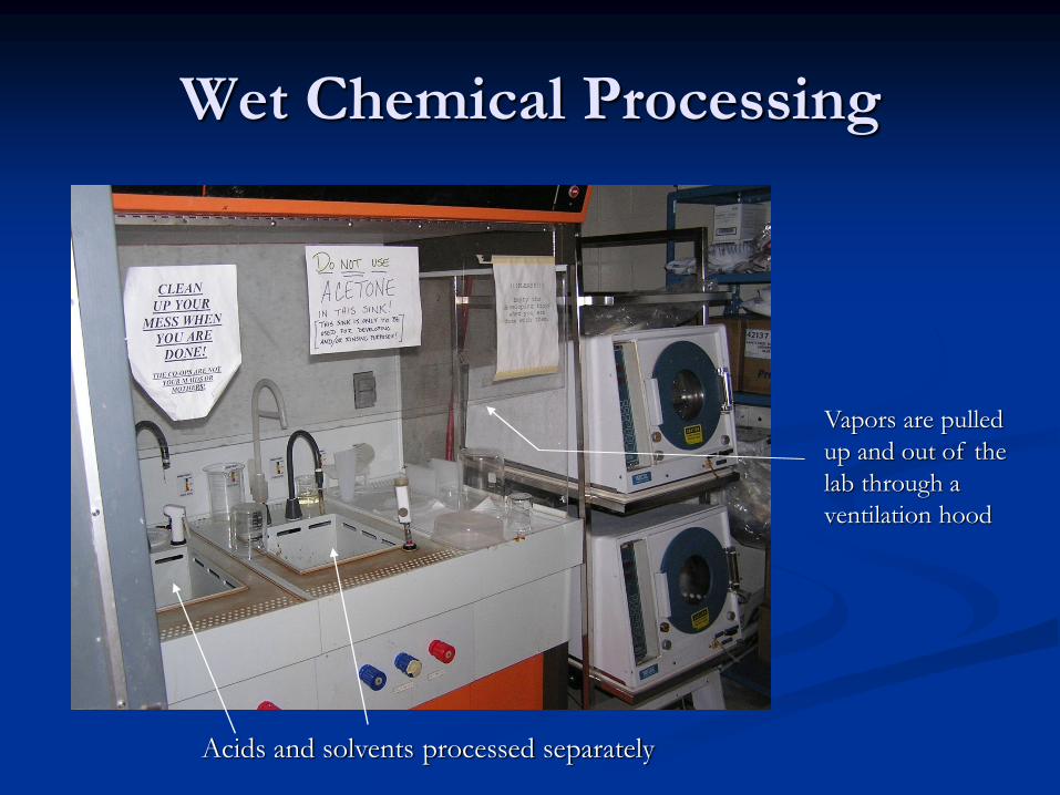
Wet Chemical Processing
Acids and solvents processed separately
Vapors are pulled
up and out of the
lab through a
ventilation hood

When Acids and Solvents Mix
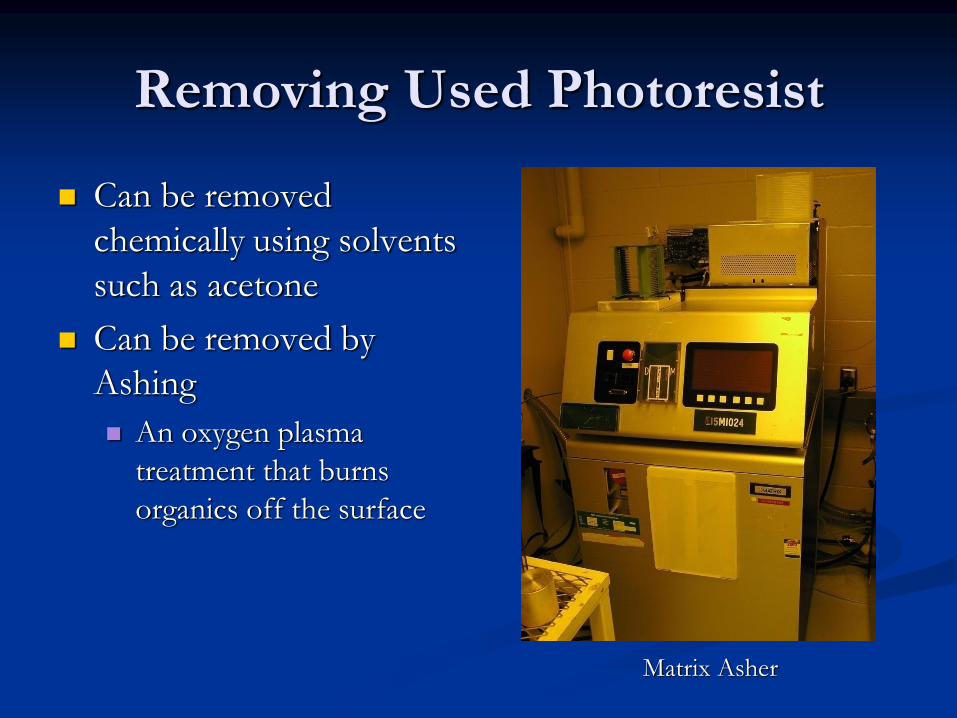
Removing Used Photoresist
Can be removed
chemically using solvents
such as acetone
Can be removed by
Ashing
An oxygen plasma
treatment that burns
organics off the surface
Matrix Asher
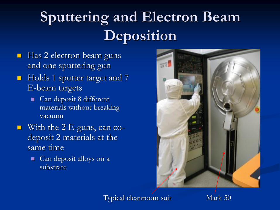
Sputtering and Electron Beam
Deposition Has 2 electron beam guns
and one sputtering gun
Holds 1 sputter target and 7 E-beam targets
Can deposit 8 different materials without breaking vacuum
With the 2 E-guns, can co-deposit 2 materials at the same time
Can deposit alloys on a substrate
Typical cleanroom suit Mark 50
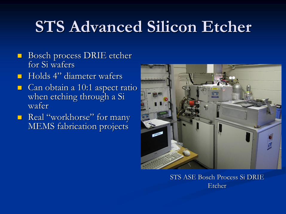
STS Advanced Silicon Etcher
Bosch process DRIE etcher for Si wafers
Holds 4” diameter wafers
Can obtain a 10:1 aspect ratio when etching through a Si wafer
Real “workhorse” for many MEMS fabrication projects
STS ASE Bosch Process Si DRIE
Etcher
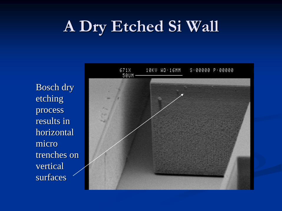
A Dry Etched Si Wall
Bosch dry
etching
process
results in
horizontal
micro
trenches on
vertical
surfaces
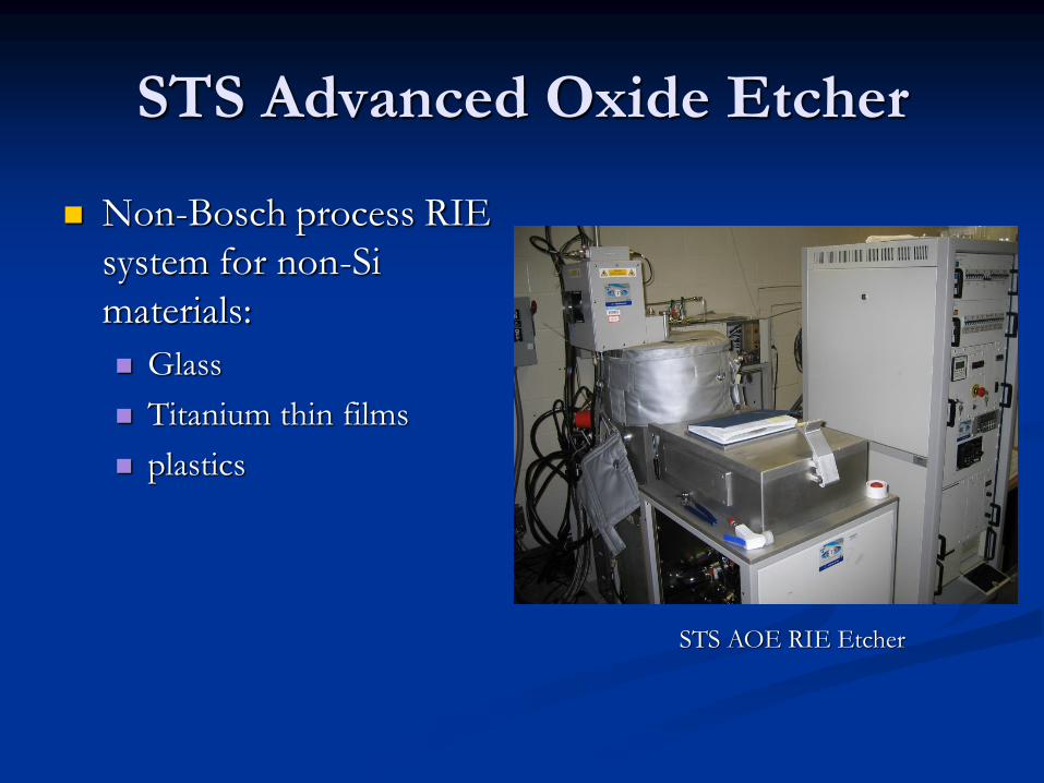
STS Advanced Oxide Etcher
Non-Bosch process RIE
system for non-Si
materials:
Glass
Titanium thin films
plastics
STS AOE RIE Etcher
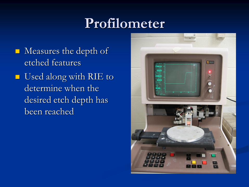
Profilometer
Measures the depth of
etched features
Used along with RIE to
determine when the
desired etch depth has
been reached
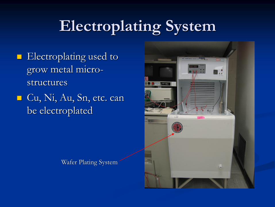
Electroplating System
Electroplating used to
grow metal micro-
structures
Cu, Ni, Au, Sn, etc. can
be electroplated
Wafer Plating System
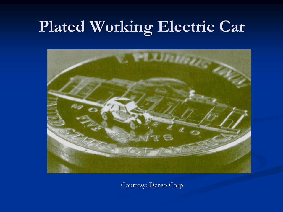
Plated Working Electric Car
Courtesy: Denso Corp
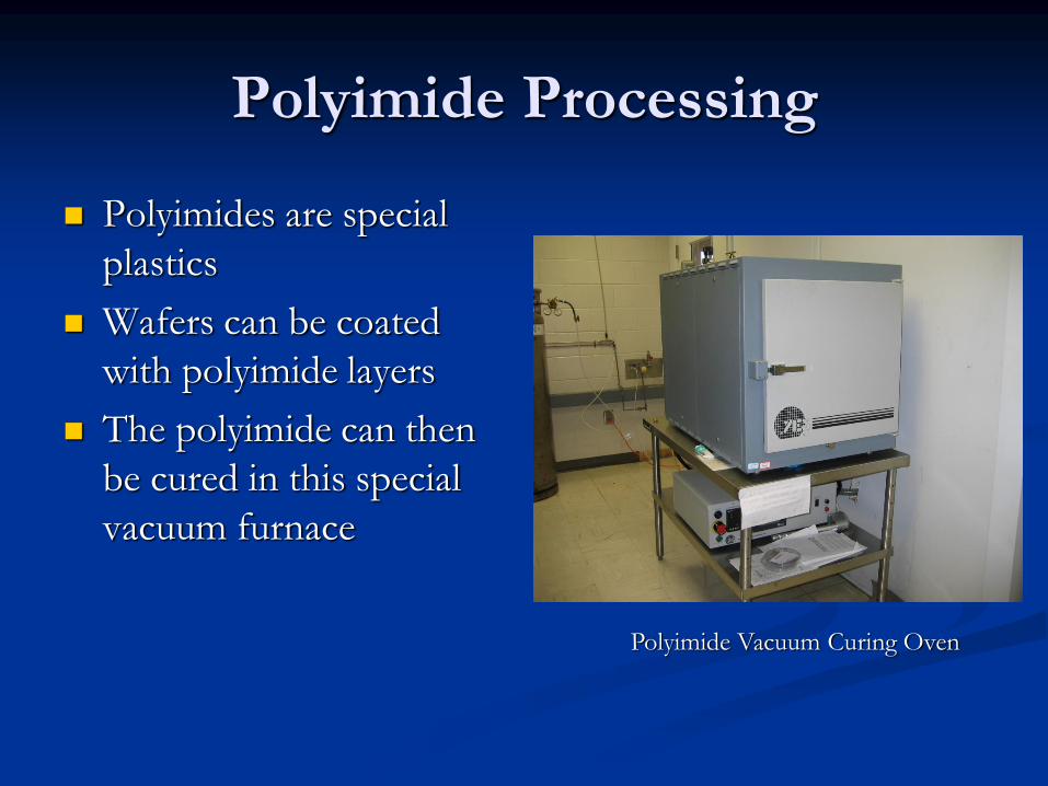
Polyimide Processing
Polyimides are special
plastics
Wafers can be coated
with polyimide layers
The polyimide can then
be cured in this special
vacuum furnace
Polyimide Vacuum Curing Oven
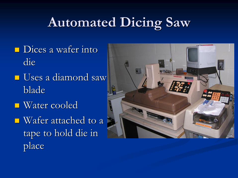
Automated Dicing Saw
Dices a wafer into
die
Uses a diamond saw
blade
Water cooled
Wafer attached to a
tape to hold die in
place
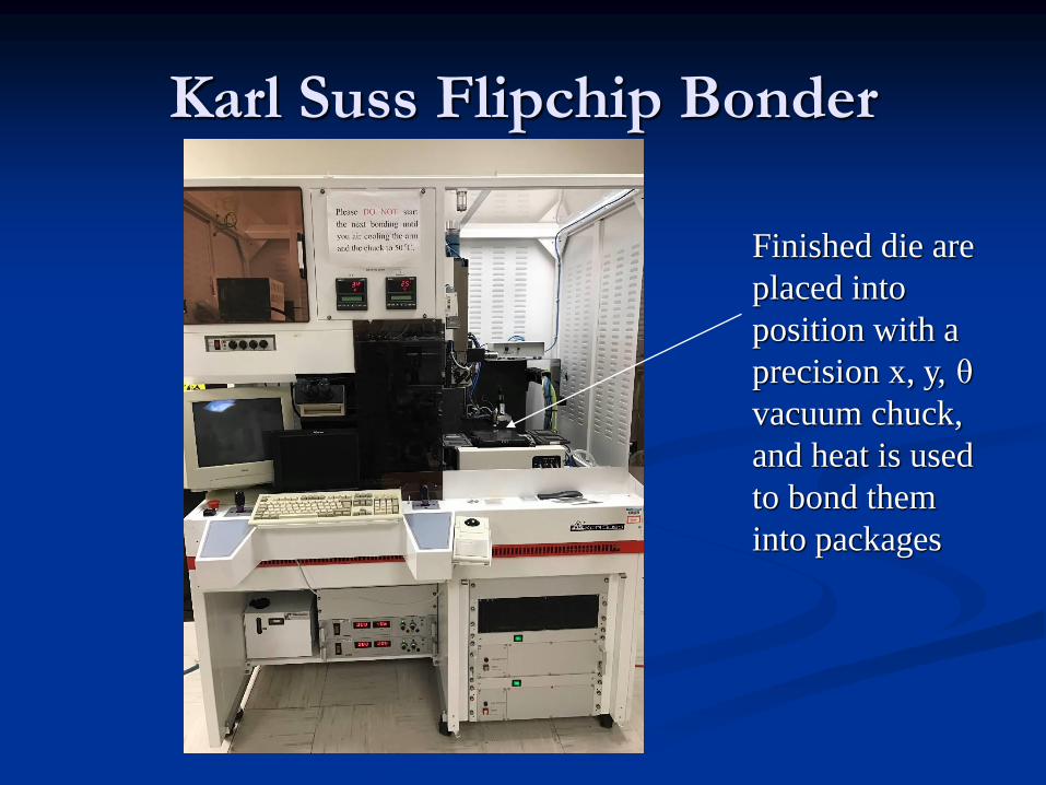
Karl Suss Flipchip Bonder
Finished die are
placed into
position with a
precision x, y, θ
vacuum chuck,
and heat is used
to bond them
into packages
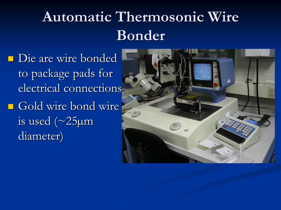
Automatic Thermosonic Wire
Bonder
Die are wire bonded
to package pads for
electrical connections
Gold wire bond wire
is used (~25µm
diameter)
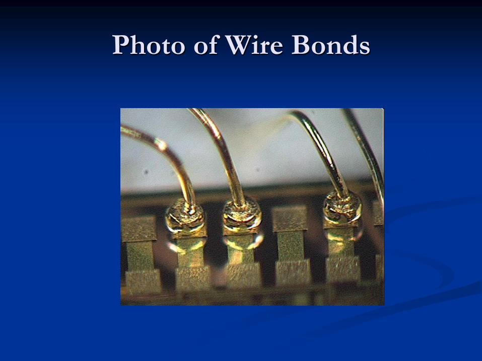
Photo of Wire Bonds
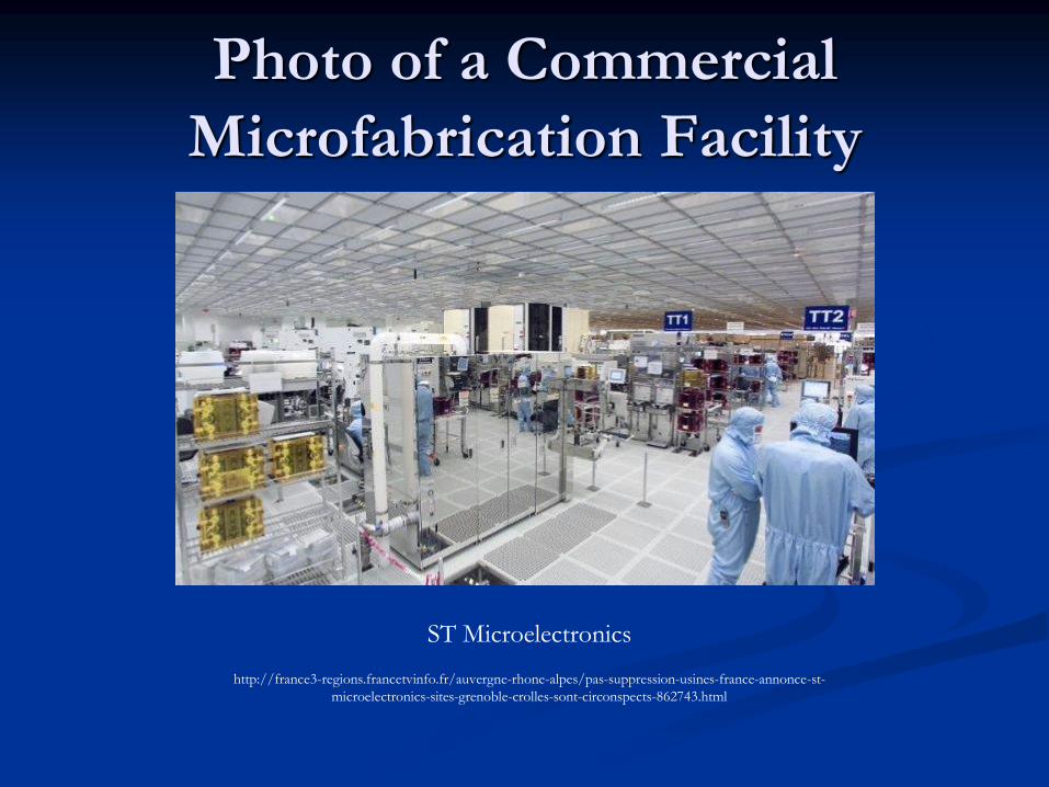
Photo of a Commercial
Microfabrication Facility
ST Microelectronics
http://france3-regions.francetvinfo.fr/auvergne-rhone-alpes/pas-suppression-usines-france-annonce-st-
microelectronics-sites-grenoble-crolles-sont-circonspects-862743.html

The End