Embed Size (px)
Citation preview
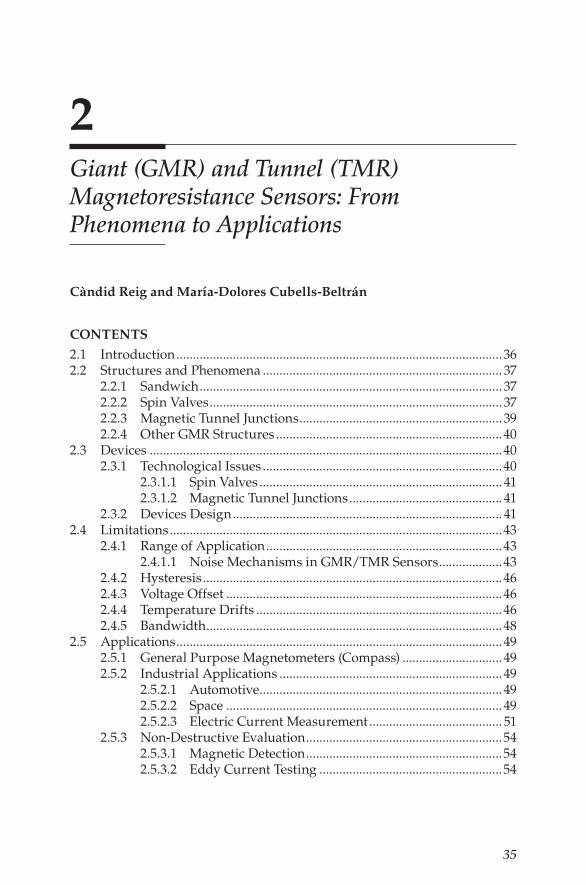
35
2Giant (GMR) and Tunnel (TMR) Magnetoresistance Sensors: From Phenomena to Applications
Cà ndid Reig and Marí a-Dolores Cubells-Beltrá n
CONTENTS
2.1 Introduction ..................................................................................................362.2 Structures and Phenomena ........................................................................ 37
2.2.1 Sandwich ........................................................................................... 372.2.2 Spin Valves ........................................................................................ 372.2.3 Magnetic Tunnel Junctions ............................................................. 392.2.4 Other GMR Structures ....................................................................40
2.3 Devices ..........................................................................................................402.3.1 Technological Issues ........................................................................40
2.3.1.1 Spin Valves ......................................................................... 412.3.1.2 Magnetic Tunnel Junctions .............................................. 41
2.3.2 Devices Design ................................................................................. 412.4 Limitations ....................................................................................................43
2.4.1 Range of Application .......................................................................432.4.1.1 Noise Mechanisms in GMR/TMR Sensors ...................43
2.4.2 Hysteresis ..........................................................................................462.4.3 Voltage Offset ...................................................................................462.4.4 Temperature Drifts ..........................................................................462.4.5 Bandwidth .........................................................................................48
2.5 Applications .................................................................................................. 492.5.1 General Purpose Magnetometers (Compass) .............................. 492.5.2 Industrial Applications ................................................................... 49
2.5.2.1 Automotive ......................................................................... 492.5.2.2 Space ................................................................................... 492.5.2.3 Electric Current Measurement ........................................ 51
2.5.3 Non-Destructive Evaluation ...........................................................542.5.3.1 Magnetic Detection ...........................................................542.5.3.2 Eddy Current Testing .......................................................54
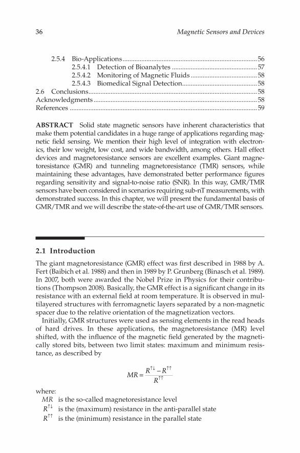
36 Magnetic Sensors and Devices
ABSTRACT Solid state magnetic sensors have inherent characteristics that make them potential candidates in a huge range of applications regarding mag-netic field sensing. We mention their high level of integration with electron-ics, their low weight, low cost, and wide bandwidth, among others. Hall effect devices and magnetoresistance sensors are excellent examples. Giant magne-toresistance (GMR) and tunneling magnetoresistance (TMR) sensors, while maintaining these advantages, have demonstrated better performance figures regarding sensitivity and signal-to-noise ratio (SNR). In this way, GMR/TMR sensors have been considered in scenarios requiring sub-nT measurements, with demonstrated success. In this chapter, we will present the fundamental basis of GMR/TMR and we will describe the state-of-the-art use of GMR/TMR sensors.
2.1 Introduction
The giant magnetoresistance (GMR) effect was first described in 1988 by A. Fert (Baibich et al. 1988) and then in 1989 by P. Grunberg (Binasch et al. 1989). In 2007, both were awarded the Nobel Prize in Physics for their contribu-tions (Thompson 2008). Basically, the GMR effect is a significant change in its resistance with an external field at room temperature. It is observed in mul-tilayered structures with ferromagnetic layers separated by a non-magnetic spacer due to the relative orientation of the magnetization vectors.
Initially, GMR structures were used as sensing elements in the read heads of hard drives. In these applications, the magnetoresistance (MR) level shifted, with the influence of the magnetic field generated by the magneti-cally stored bits, between two limit states: maximum and minimum resis-tance, as described by
MRR R
R= −↑↓ ↑↑
↑↑
where: MR is the so-called magnetoresistance level R↑↓ is the (maximum) resistance in the anti-parallel state R↑↑ is the (minimum) resistance in the parallel state
2.5.4 Bio-Applications ...............................................................................562.5.4.1 Detection of Bioanalytes .................................................. 572.5.4.2 Monitoring of Magnetic Fluids .......................................582.5.4.3 Biomedical Signal Detection ............................................58
2.6 Conclusions ...................................................................................................58Acknowledgments ................................................................................................58References .............................................................................................................. 59
37Giant and Tunnel MR Sensors
Nowadays, these multilayered structures can be engineered in such a way that the quiescent state of the structure is obtained with layers having their magnetic moments in a crossed-axis (orthogonal) confi guration by means of a particular deposition process or by the application of an external magnetic biasing. In this way, the transfer curve of the device is notably smoothed, and the quiescent working point is placed in a medium state, thereby providing a useful quasi-linear region that can be utilized for analog magnetic sensing applications.
2.2 Structures and Phenomena
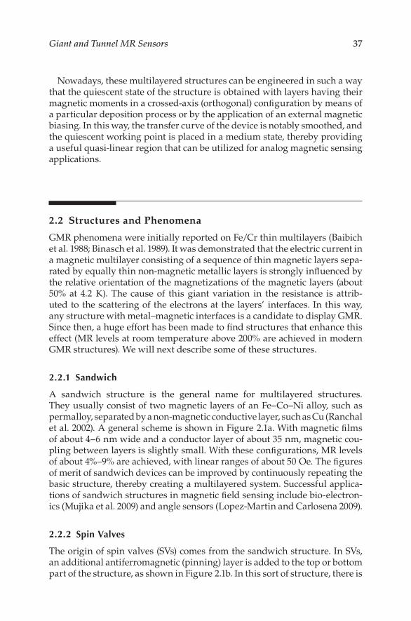
GMR phenomena were initially reported on Fe/Cr thin multilayers (Baibich et al. 1988; Binasch et al. 1989). It was demonstrated that the electric current in a magnetic multilayer consisting of a sequence of thin magnetic layers sepa-rated by equally thin non-magnetic metallic layers is strongly infl uenced by the relative orientation of the magnetizations of the magnetic layers (about 50% at 4.2 K). The cause of this giant variation in the resistance is attrib-uted to the scattering of the electrons at the layers’ interfaces. In this way, any structure with metal–magnetic interfaces is a candidate to display GMR. Since then, a huge effort has been made to find structures that enhance this effect (MR levels at room temperature above 200% are achieved in modern GMR structures). We will next describe some of these structures.
2.2.1 Sandwich
A sandwich structure is the general name for multilayered structures. They usually consist of two magnetic layers of an Fe–Co–Ni alloy, such as permalloy, separated by a non-magnetic conductive layer, such as Cu (Ranchal et al. 2002). A general scheme is shown in Figure 2.1a. With magnetic fi lms of about 4–6 nm wide and a conductor layer of about 35 nm, magnetic cou-pling between layers is slightly small. With these confi gurations, MR levels of about 4%–9% are achieved, with linear ranges of about 50 Oe. The fi gures of merit of sandwich devices can be improved by continuously repeating the basic structure, thereby creating a multilayered system. Successful applica-tions of sandwich structures in magnetic fi eld sensing include bio-electron-ics (Mujika et al. 2009) and angle sensors (Lopez-Martin and Carlosena 2009).
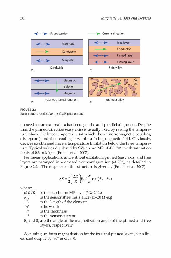
2.2.2 Spin Valves
The origin of spin valves (SVs) comes from the sandwich structure. In SVs, an additional antiferromagnetic (pinning) layer is added to the top or bottom part of the structure, as shown in Figure 2.1b. In this sort of structure, there is
38 Magnetic Sensors and Devices
no need for an external excitation to get the anti-parallel alignment. Despite this, the pinned direction (easy axis) is usually fi xed by raising the tempera-ture above the knee temperature (at which the antiferromagnetic coupling disappears) and then cooling it within a fi xing magnetic fi eld. Obviously, devices so obtained have a temperature limitation below the knee tempera-ture. Typical values displayed by SVs are an MR of 4%–20% with saturation fi elds of 0.8–6 kA/m (Freitas et al. 2007).
For linear applications, and without excitation, pinned (easy axis) and free layers are arranged in a crossed-axis confi guration (at 90° ), as detailed in Figure 2.2a. The response of this structure is given by (Freitas et al. 2007)
∆ ∆R
RR
R iWh
sq p f=
−( )12
cos θ θ
where: (Δ R /R ) is the maximum MR level (5%–20%) R sq is the sensor sheet resistance (15–20 Ω /sq) L is the length of the element W is its width h is the thickness i is the sensor current θ p and θ f are the angle of the magnetization angle of the pinned and free
layers, respectively
Assuming uniform magnetization for the free and pinned layers, for a lin-earized output, θ p =90° and θ f =0.
Magnetization Current direction
Magnetic Free layer
Conductor
Pinned layer
Pinning layerMagnetic
Sandwich(a) (b)
(c) (d)
Spin valve
Conductor
Magnetic CuAg
CoMagnetic
Magnetic tunnel junction Granular alloy
Isolator
FIGURE 2.1 Basic structures displaying GMR phenomena.
39Giant and Tunnel MR Sensors
2.2.3 Magnetic Tunnel Junctions
Magnetic tunnel junctions (MTJ), also called tunnel magnetoresistance (TMR) structures, were initially described as GMR structures (Hirota et al. 2002). Nowadays, they are considered a specific MR effect (Reig et al. 2013). Nevertheless, due to the similarity of both families of structures and their shared applications, we will also consider them in this chapter.
In this case, the magnetic layers are separated not by a conductive layer but by a very thin isolating layer, following a current perpendicular to planes (CPP) confi guration (see Figures 2.1c and 2.2b). Electrons can cross this thin fi lm by means of the quantum tunnel effect. As deduced from quan-tum mechanics arguments, the crossing probability is higher when both magnetic moments are aligned in parallel and lower when both magnetic moments are not aligned in parallel. The equation describing the output of these structures is
PinningPinnedSpacerFree
θp θf
(a)
(b)
PinningPinnedSpacerFree
θpθf
FIGURE 2.2 Multilayer structures corresponding to typical spin valves (a) and magnetic tunnel junctions (b).
40 Magnetic Sensors and Devices
∆V TMR= × −( )12
cosiR AWh
p fθ θ
where: TMR is the maximum MR level i is the biasing current R × A is the resistance per area parameter Wh are the dimensions
These devices usually make use of the SV principle in order to fi x the easy axis by means of a pinning antiferromagnetic layer. Typical MR levels of MTJ are above 40%, with Al2 O3 as the isolating layer (Ziese and Thornton 2001). More recently, MR levels of about 200% have been reported for MgO-based structures (Ferreira et al. 2006). Saturation fi elds are of the order of 1− 100 Oe. The basis of linear MTJs is analogous to that of a linear SV. When confi gured in a crossed-axis confi guration, linear ranges suitable for sensor applications can be achieved (Freitas et al. 2007).
2.2.4 Other GMR Structures
Granular fi lms of Co–Cu and Co–Ag also exhibit a GMR effect. In this case, the GMR effect is due to the spin-dependent scattering taking place at the boundaries of Co clusters embedded in the host lattice, as depicted in Figure 2.1d. Because these binary systems are not miscible, the characteris-tics of the devices are highly conditioned by the growth conditions and the post-deposition treatments. In fact, the amount of MR is accepted to be asso-ciated with the size of the Co clusters (André s et al. 1999).
GMR can also be found in other structures. We collected two illustrative examples. Pena et al. (2005) report on GMR in ferromagnet/superconductor superlattices and Pullini et al. (2007) describe GMR in multilayered nanow-ires. In any case, a magnetic–non-magnetic interface is required in order to allow the spin-electron scattering to produce the effect.
2.3 Devices
In order to have functional devices, GMR/TMR multilayered structures have to be patterned into elements with proper resistance values for use as sensors. Then, these elements need to be contacted.
2.3.1 Technological Issues
The deposition of these structures can be done with low temperature pro-cesses and then patterned by selective physical etching, so avoiding damage
41Giant and Tunnel MR Sensors
in the substrate. In this sense, the deposition of these structures can be accomplished by ion beam deposition (IBD) or by sputtering. In any case, the substrate temperature does not exceed 120° C. Thus, both processes can be directly masked with photoresist without damaging the substrate. In some cases, a fi nal heat treatment of between 200° C and 300° C is required to increase the MR ratio (He et al. 2010).
2.3.1.1 Spin Valves
A typical structure can be found in Reig et al. (2004). It was deposited by ion beam sputtering (IBD) onto a 3″ Si/SiO2 1500 Å substrate. The SV structure was Ta (20 Å )/NiFe (30 Å )/CoFe (20 Å )/Cu (22 Å )/CoFe (25 Å )/MnIr (60 Å )/Ta (40 Å ). This structure was demonstrated to give MR responses of about 6%–7%, linear ranges of about 20 Oe, and sheet resistivities of about 10–15 Ω /sq. Deposition rates ranged from 0.3 to 0.6 Å /s. A 40 Oe fi eld was applied to the substrates during the deposition step in order to state the easy axis in the pinned and free layers. The wafer was rotated 90° between both depositions to ensure a crossed-axis SV confi guration.
Nano-oxide layers (NOL) inserted in the pinned layer and above the free layer have been found to increase the MR ratio (Reig et al. 2005). The enhance-ment of GMR is attributed to the specular scattering effect of the conduction electrons at the metal–insulator interfaces.
2.3.1.2 Magnetic Tunnel Junctions
A typical MTJ structure was deposited by ion beam sputtering (IBD) onto 3″ Si/SiO2 1000 Å substrates. The fi nal structure of the MTJ was Al (600 Å )/Ta (90 Å )/NiFe (70 Å )/MnIr (250 Å )/CoFe (50 Å )/Al2 O3 (12 Å )/CoFe (50 Å )/NiFe (25 Å )/Ta (60 Å )/TiW (300 Å ), as described in Reig et al. (2008). This particular structure was demonstrated to give MR responses close to 40% while keeping linear ranges above 20 Oe.
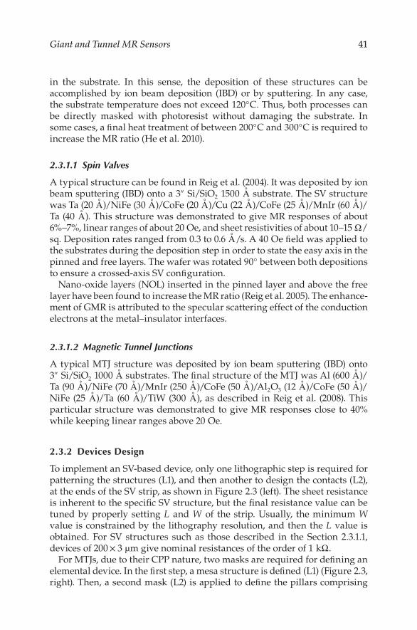
2.3.2 Devices Design
To implement an SV-based device, only one lithographic step is required for patterning the structures (L1), and then another to design the contacts (L2), at the ends of the SV strip, as shown in Figure 2.3 (left). The sheet resistance is inherent to the specific SV structure, but the final resistance value can be tuned by properly setting L and W of the strip. Usually, the minimum W value is constrained by the lithography resolution, and then the L value is obtained. For SV structures such as those described in the Section 2.3.1.1, devices of 200 × 3 µ m give nominal resistances of the order of 1 kΩ .
For MTJs, due to their CPP nature, two masks are required for defi ning an elemental device. In the fi rst step, a mesa structure is defi ned (L1) (Figure 2.3, right). Then, a second mask (L2) is applied to defi ne the pillars comprising
42 Magnetic Sensors and Devices
the active region. Usually, a conductive bottom layer is included in the mul-tilayered structure to connect devices in pairs, and facilitating the electrical contacts on the top of the structures (L3).
Because these elements are resistance, once they have been defined, they can be arranged in different configurations, depending on the specific requirement. MTJs are commonly arranged in arrays of elements in series and parallel, due to their better SNR performance and the intrinsic depen-dence of the MR level with the voltage bias (Chen and Freitas 2012).
In linear applications involving resistive sensors, bridge setups are often considered. They display a highly linear response, a better signal level, zeroed output, and high immunity to undesired external effects. Successful examples of the use of GMR/TMR sensors configured as bridges can be found in Cubells-Beltrá n et al. (2009), Guerrero et al. (2009), and Le Phan et al. (2005).
When magnetic imaging is the objective, GMR sensors can also be arranged in arrays, as described, for example, by Cardoso et al. (2006), where MTJ elements have been integrated with a thin-film transistor (TFT) diode for improving the addressing process, or in Hall et al. (2013), where 256 pixels arrays with integrated complementary metal-oxide semiconductor (CMOS) circuitry have been demonstrated.
Silicon
L1
L2
L1
L2
L3
Silicon oxide
Aluminum
Spin valve multilayered structure
Magnetic tunnel junction multilayered structure
Fabrication process of the elemental devices
Spin valves (SV) Magnetic tunnel junctions (MTJ)
FIGURE 2.3 GMR/TMR basic fabrication steps.
43Giant and Tunnel MR Sensors
2.4 Limitations
The limitations of use of these sensors arise from very different reasons including the range of application, reproducibility, voltage offset, tempera-ture drifts, or bandwidth constrictions. In the following sections, we describe some of these limitations and we give the direction of current investigations for overcoming them.
2.4.1 Range of Application
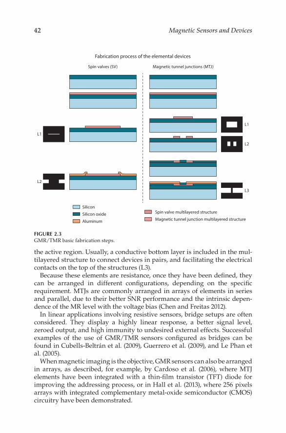
The intrinsically useful range of MR-based sensors is mainly limited by two mechanisms. At the low-level region, the SNR ratio sets the detection limit. Then, a study of the related noise sources is mandatory. The noise power spectrum density (PSD) is commonly given in square volts per hertz (V2 /Hz). Often, it is much more convenient to use the amplitude spectrum den-sity (ASD), expressed in volts per square root hertz (V/√ Hz), for a compar-ison with voltage signals. The sensitivity for an MR signal, S V , is usually given in V/V/T. Typical values for GMR sensors are 20–40 V/V/T, for exam-ple, 20–40 nV/nT when they are biased with 1 V. For comparing diff erent sensors, it is recommended to use the fi eld equivalent noise power spectra density, sometimes called detectivity . It corresponds to the PSD divided by the sensitivity. For example, if a sensor displays a noise of 10 nV/√ Hz at a given frequency and a sensitivity of 25 V/V/T, its detectivity will be 400 pT for 1 V bias (Reig et al. 2013). At the high signal region, the saturation fi eld is the limitation mechanism. For sensing applications, a good approximation is to consider the linear range to be one-half of the saturation fi eld.
GMR/TMR can be applied in the range from some petatesles (pT) to almost kilotesles (kT), which is more than 14 orders of magnitude, as observed in Figure 2.4, compared with other magnetic sensors.
2.4.1.1 Noise Mechanisms in GMR/TMR Sensors
2.4.1.1.1 Thermal Noise
The most relevant noise is the thermal noise (also called the Johnson–Nyquist noise or white noise), which is directly related to the resistance of the sensor. It is a white noise, so it is independent of the frequency. It was fi rst observed by Johnson (1928) and interpreted by Nyquist (1928). It is expressed as
S Rk TV Bω( ) = 4
where: R is the sensor resistance k B is the Boltzmann constant T is the temperature
44 Magnetic Sensors and Devices
For example, a 1 kΩ resistor at room temperature has 4 nV/√ Hz.
2.4.1.1.2 1/f Noise
The origin of the 1/f noise or “ pink” noise or Flicker noise is from resistance fl uctuations, so it can only be revealed by applying a current to the sensor. Its dependence with the frequency is described by the following phenom-enological formula:
SR I
N fV
H
cω γ
β( ) =2 2
where: γ H is a dimensionless constant proposed by Hooge (1976) R is the sensor resistance I is the bias current N c is the number of current carriers f is the frequency β is an exponent typically of the order of 1
1/f noise can exhibit a non-magnetic and a magnetic component with pos-sible diff erent slopes. For TMRs, the formula becomes
SR IA f
V ω α( ) =2 2
Magnetic diodeMagnetic transistor
Hall GMREMR
MagnetostrictionMTJ
Magneto opticalGMI
Optical �berAMR
FluxgateNuclear presession
Optical pumpingSearch coil
SQUID
1 fT 1 pT 1 nT 1 µT 1 mT 1 T 1 kT
Tomography
Variationof Earth
magnetic�eld
NDE
Magnetic �eld range
DetectionY/N
Detectionguidance
of vehicles
Positionsensing
Navigation
Archeologysupercond.
Rotation
FIGURE 2.4 Range of applications of different magnetic field sensors. (From Dí az-Michelena, M., Sensors [Basel, Switzerland], 9(4), 2271–88, 2009.)
45Giant and Tunnel MR Sensors
where: A is the active surface of the device α is a parameter with the dimension of a surface
The size and shape of the sensors have a strong eff ect on the 1/f noise.In GMRs and TMRs, this low-frequency noise is dominant and is often a
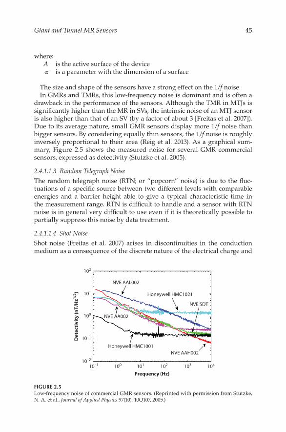
drawback in the performance of the sensors. Although the TMR in MTJs is signifi cantly higher than the MR in SVs, the intrinsic noise of an MTJ sensor is also higher than that of an SV (by a factor of about 3 [Freitas et al. 2007]). Due to its average nature, small GMR sensors display more 1/f noise than bigger sensors. By considering equally thin sensors, the 1/f noise is roughly inversely proportional to their area (Reig et al. 2013). As a graphical sum-mary, Figure 2.5 shows the measured noise for several GMR commercial sensors, expressed as detectivity (Stutzke et al. 2005).
2.4.1.1.3 Random Telegraph Noise
The random telegraph noise (RTN; or “ popcorn” noise) is due to the fluc-tuations of a specific source between two different levels with comparable energies and a barrier height able to give a typical characteristic time in the measurement range. RTN is difficult to handle and a sensor with RTN noise is in general very difficult to use even if it is theoretically possible to partially suppress this noise by data treatment.
2.4.1.1.4 Shot Noise
Shot noise (Freitas et al. 2007) arises in discontinuities in the conduction medium as a consequence of the discrete nature of the electrical charge and
Honeywell HMC1001
10–110–2
10–1
100
101
102
100 101 102 103 104
Honeywell HMC1021
NVE AAL002
Frequency (Hz)
Det
ecti
vity
(nT/
Hz1/
2 )
NVE SDT
NVE AA002
NVE AAH002
FIGURE 2.5 Low-frequency noise of commercial GMR sensors. (Reprinted with permission from Stutzke, N. A. et al., Journal of Applied Physics 97(10), 10Q107, 2005.)
46 Magnetic Sensors and Devices
is described by the following equation, where e stands for the electron elec-trical charge and I is the current flowing through the device (for practical device operating temperatures).
S e I RV ω( ) = 2 2
The tunnel barrier of an MTJ is an example of a discontinuity in the con-duction medium, which is why shot noise is found in MTJs but not in SVs or anisotropic magnetoresistance (AMR) sensors, which are made of continu-ous metallic layers.
2.4.2 Hysteresis
The magnetic nature of GMR-based sensors implies an associated hyster-esis. Such effect has been analyzed for GMR sensors both numerically (Á č 2008) and experimentally (Liu et al. 2012). Intrinsically, this inherent hys-teresis can be internally reduced by considering a so-called crossed-axis confi guration of the magnetization moments of the constituent layers of the MR structure. In this case, since the free layer would never reverse, but merely displace by 90° , hysteretic errors below 1% of the full scale can be achieved (Reig et al. 2004). Alternating current (ac) biasing schemes have been proposed for reducing the hysteresis. In Ripka et al. (1999), by using an ac biasing of 5 mA at 10 kHz, the hysteresis of a commercial NVE sen-sor was reduced from 5% to 1% in the 0.3 mT range. In addition, both SNR and offset were also partially reduced. Hysteresis has also been reduced by biasing the sensors with an external magnetic fi eld (Vopá lenský et al. 2004). More recently, electrical models have been developed to reduce the hysteresis in specific GMR-based current sensors (Jedlicska et al. 2010; Han et al. 2015).
2.4.3 Voltage Offset
MR sensors are commonly used in a bridge confi guration, so voltage off-sets are introduced during the fabrication process. Common sources of these deviations are deposition inhomogeneities and lithography tolerances. As the dimensions of MR structures are close to the lithography resolution limit, these tolerances need to be externally corrected using external circuits.
2.4.4 Temperature Drifts
Temperature is always a limiting parameter in electronics. Every electronic device has a temperature-dependent response arising from its physical nature. Regarding specifi c GMR sensors, not only does the resistance (and the sensor impedance) vary with the temperature, but so does the MR level (and then the sensitivity).
47Giant and Tunnel MR Sensors
The resistance of GMR sensors is a function of the temperature. For GMR-based devices, and in the usual range of utilization, this dependence can be considered linear, and can be defi ned by a temperature coeffi cient (TEMPCO) as follows:
TCR %( ) = ×1001
0RRTT
∆∆
An analog relationship can be defi ned for the thermal dependence of sen-sitivity as
TCSS
%( ) = ×1001
0S TT
∆∆
When a full bridge confi guration is considered, this thermal dependence is partially compensated and is expected to be low. Due to the inherent voltage offset of sensors confi gured as bridges, the temperature drift of the offset voltage must be specifi ed:
TCVoff
off
off%
,( ) = ×100
0
∆∆VT
V T
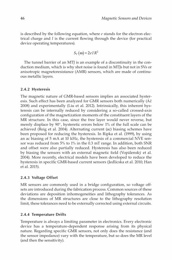
MR structures are temperature dependent. For real applications, the temperature coeffi cient of the output voltage of a given sensor can be set below 0.1%/K in a Wheatstone bridge confi guration with a direct cur-rent (dc) bias instead of a direct voltage bias (Cubells-Beltrá n et al. 2011). Experimental parameters are only related to the nature of the GMR struc-tures, and they have been measured elsewhere. In Figure 2.6, we show the typical values for full bridge sensors composed of equal SV elements, as
0.95
–20°C 0°C 20°C
Normalized Zinp
40°C 60°C
1.00
1.05
0.8
–20°C
0.9
1.0
1.1
1.2
0°C 20°C
Normalized S
40°C 60°C
–0.4
–20°C
–0.2
0.0
0.2
0.4
0°C 20°C
DVo� (mV)
40°C 60°C
FIGURE 2.6 Temperature dependence of the characteristic parameters in typical spin valves. (From Cubells-Beltrá n, M. et al., IEEE Sensors Journal, 9(12), 1756–62, 2009.)
48 Magnetic Sensors and Devices
described in Cubells-Beltrá n et al. (2009). From these graphs, we can extract TCR ≈ 0.11%/° C, TCVoff < 10 µ V/° C, and TCS ≈ − 0.15%/° C, as they were defined before.
When thermal drifts are not sufficiently lowered by using bridge configu-rations, different temperature compensation schemes have been proposed in the literature, specifically developed for GMR sensors–based applications (Rami rez Mun oz et al. 2006; Sá nchez Moreno et al. 2011).
2.4.5 Bandwidth
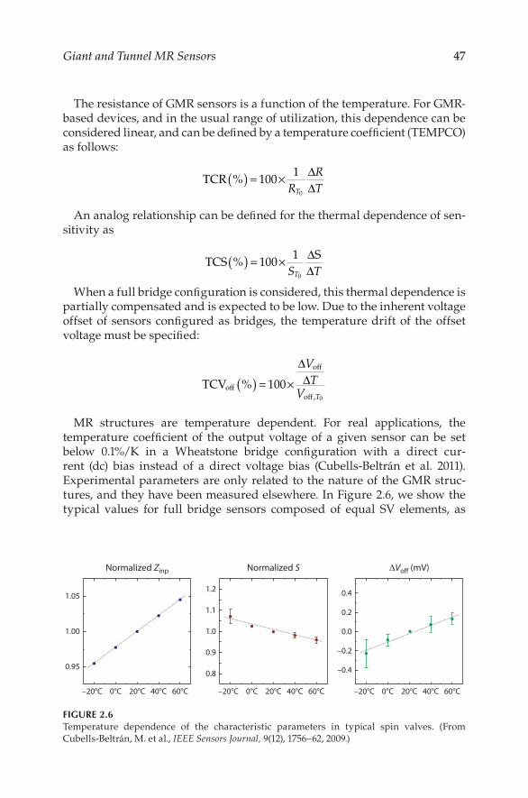
Theoretically, due to the inherent quantum mechanism involved, MR struc-tures have bandwidths of the order of 1 GHz (Hirota et al. 2002). In real applications, a reduction in the bandwidth is introduced by the associated circuitry. Such an effect can be important in electric current monitoring appli-cations because of the necessity to drive the current path close to the sensor. In principle, due to the inductive character of the coupling, a “ zero” behav-ior in the transfer function should be observed. In Figure 2.7, the frequency responses of some illustrative examples are compiled: an HMC1O21 sensor soldered onto a typical (3 mm width) printed circuit board (PCB) strap, a meandered engineered SV sensor (Reig et al. 2004), and an MTJ compact current sensor prototype both in a full Wheatstone bridge confi guration and a single resistor (Reig et al. 2008). As observed, an inductive effect appears well below 1 MHz. Moreover, the more complicated the sensing structure is, the less bandwidth obtained. Regarding real applications, MR current sen-sors have been successfully applied up to 1 MHz (Cubells-Beltrá n et al. 2009; Singh and Khambadkone 2014).
3
2
1
1 10
HMC1021 (onto a single PCB current track)Meandered engineered spin valve sensorMTJ (full bridge con�guration)MTJ (stand-alone resistor)
Frequency (kHz)
Nor
mal
ized
out
put v
olta
ge
100
FIGURE 2.7 Frequency dependence of some selected GMR/MTJ current sensors. (From Cubells-Beltrá n, M.-D. et al., International Review of Electrical Engineering (IREE) 6(1), 423–29, 2011.)
49Giant and Tunnel MR Sensors
2.5 Applications
Now that we have described the principal characteristics of GMR/TMR sen-sors, we will describe some real applications in which these sensors have demonstrated their intrinsic capabilities.
2.5.1 General Purpose Magnetometers (Compass)
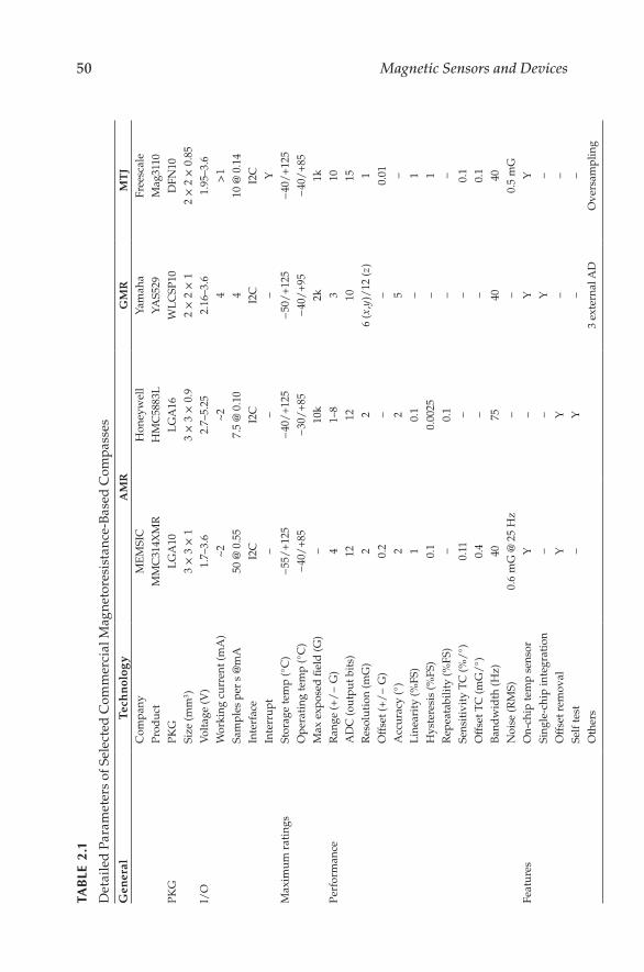
The measurement of the Earth’ s magnetic field is the ancient application of magnetic field sensors. The Earth’ s magnetic field ranges between approxi-mately 25 and 60 µ T, which is well covered by GMR/TMR sensors. With the increasing demand for digital compasses for mobile applications (mainly smartphones), GMR/TMR sensors have entered the market in serious com-petition with standard Hall solutions. Table 2.1 shows the main parameters of some selected MR compasses, including electronics (Reig et al. 2013).
2.5.2 Industrial Applications
2.5.2.1 Automotive
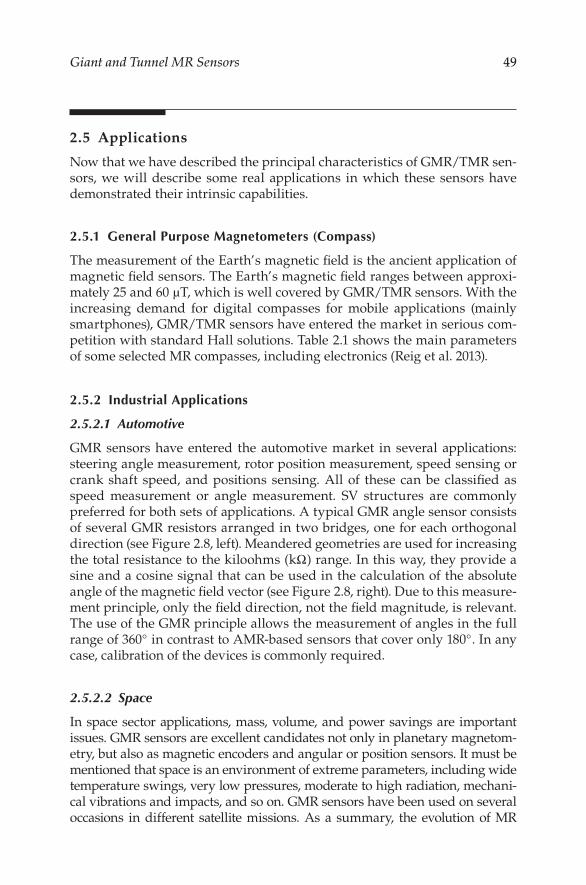
GMR sensors have entered the automotive market in several applications: steering angle measurement, rotor position measurement, speed sensing or crank shaft speed, and positions sensing. All of these can be classified as speed measurement or angle measurement. SV structures are commonly preferred for both sets of applications. A typical GMR angle sensor consists of several GMR resistors arranged in two bridges, one for each orthogonal direction (see Figure 2.8, left). Meandered geometries are used for increasing the total resistance to the kiloohms (kΩ ) range. In this way, they provide a sine and a cosine signal that can be used in the calculation of the absolute angle of the magnetic field vector (see Figure 2.8, right). Due to this measure-ment principle, only the field direction, not the field magnitude, is relevant. The use of the GMR principle allows the measurement of angles in the full range of 360° in contrast to AMR-based sensors that cover only 180° . In any case, calibration of the devices is commonly required.
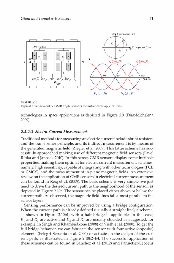
2.5.2.2 Space
In space sector applications, mass, volume, and power savings are important issues. GMR sensors are excellent candidates not only in planetary magnetom-etry, but also as magnetic encoders and angular or position sensors. It must be mentioned that space is an environment of extreme parameters, including wide temperature swings, very low pressures, moderate to high radiation, mechani-cal vibrations and impacts, and so on. GMR sensors have been used on several occasions in different satellite missions. As a summary, the evolution of MR
50 Magnetic Sensors and DevicesTA
BLE
2.1
Det
aile
d P
aram
eter
s of
Sel
ecte
d C
omm
erci
al M
agne
tore
sist
ance
-Bas
ed C
ompa
sses
Gen
eral
Tec
hn
olog
yA
MR
G
MR
M
TJ
Com
pany
ME
MSI
CH
oney
wel
lYa
mah
aFr
eesc
ale
Prod
uct
MM
C31
4XM
RH
MC
5883
LYA
S529
Mag
3110
PKG
PKG
LG
A10
LG
A16
WL
CSP
10D
FN10
Size
(mm
3 )3
× 3
× 1
3 ×
3 ×
0.9
2 ×
2 ×
12
× 2
× 0
.85
I/O
Vol
tage
(V)
1.7–
3.6
2.7–
5.25
2.16
–3.6
1.95
–3.6
Wor
king
cur
rent
(mA
)~
2~
24
> 1
Sam
ples
per
s @
mA
50 @
0.5
57.
5 @
0.1
04
10 @
0.1
4In
terf
ace
I2C
I2C
I2C
I2C
Inte
rrup
t–
––
YM
axim
um r
atin
gsSt
orag
e te
mp
(° C
)−
55/
+12
5−
40/
+12
5−
50/
+12
5−
40/
+12
5O
pera
ting
tem
p (°
C)
− 40
/+
85−
30/
+85
− 40
/+
95−
40/
+85
Max
exp
osed
fiel
d (G
)–
10k
2k1k
Perf
orm
ance
Ran
ge (+
/−
G)
41–
83
10A
DC
(out
put b
its)
1212
1015
Res
olut
ion
(mG
)2
26
(x ,y
)/12
(z )
1O
ffse
t (+
/−
G)
0.2
––
0.01
Acc
urac
y (°
)2
25
–L
inea
rity
(%FS
)1
0.1
–1
Hys
tere
sis
(%FS
)0.
10.
0025
–1
Rep
eata
bilit
y (%
FS)
–0.
1–
–Se
nsit
ivit
y T
C (%
/° )
0.11
––
0.1
Off
set T
C (m
G/
° )0.
4–
–0.
1B
and
wid
th (H
z)40
7540
40N
oise
(RM
S)0.
6 m
G @
25
Hz
––
0.5
mG
Feat
ures
On-
chip
tem
p se
nsor
Y–
YY
Sing
le-c
hip
inte
grat
ion
––
Y–
Off
set r
emov
alY
Y–
–Se
lf te
st–
Y–
–O
ther
s3
exte
rnal
AD
Ove
rsam
plin
g
51Giant and Tunnel MR Sensors
technologies in space applications is depicted in Figure 2.9 (Dí az-Michelena 2009).
2.5.2.3 Electric Current Measurement
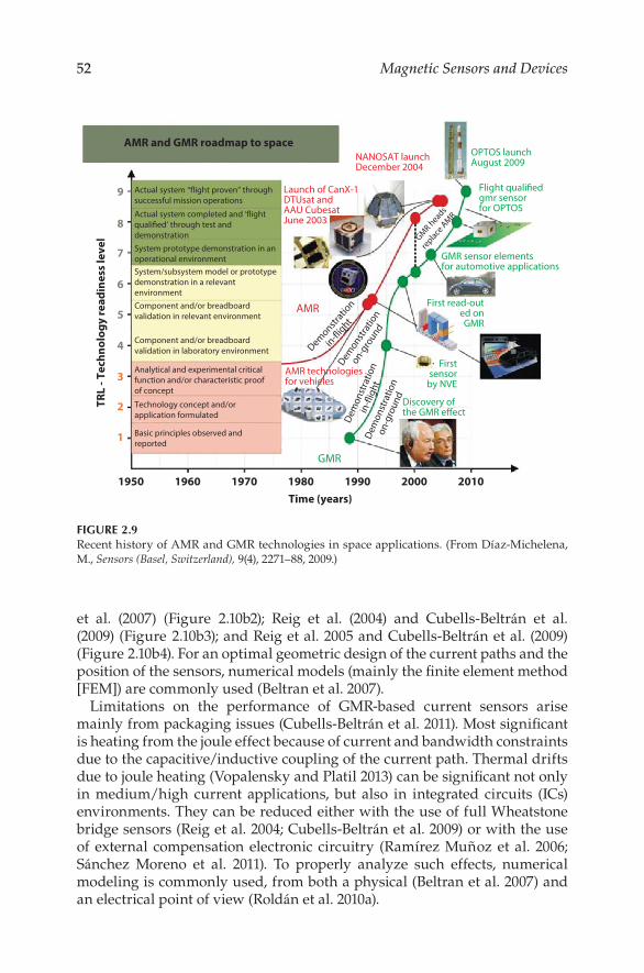
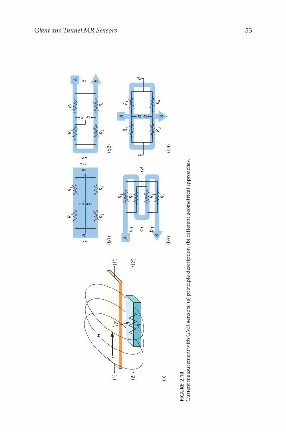
Traditional methods for measuring an electric current include shunt resistors and the transformer principle, and its indirect measurement is by means of the generated magnetic field (Ziegler et al. 2009). This latter scheme has suc-cessfully approached making use of different magnetic field sensors (Pavel Ripka and Janosek 2010). In this sense, GMR sensors display some intrinsic properties, making them optimal for electric current measurement schemes, namely, high sensitivity, capable of integrating with other technologies (PCB or CMOS), and the measurement of in-plane magnetic fields. An extensive review on the application of GMR sensors in electrical current measurement can be found in Reig et al. (2009). The basic scheme is very simple: we just need to drive the desired current path to the neighborhood of the sensor, as depicted in Figure 2.10a. The sensor can be placed either above or below the current path. As observed, the magnetic field lines fall almost parallel to the sensor layers.
Sensing performance can be improved by using a bridge configuration. When the current path is already defined (usually a straight line), a scheme, as shown in Figure 2.10b1, with a half bridge is applicable. In this case, R 1 and R 3 are active and R 2 and R 4 are usually shielded as suggested, for example, in Singh and Khambadkone (2008) or Vieth et al. (2000). To get the full bridge behavior, we can fabricate the sensor with four active (opposite) elements (Pelegri Sebastia et al. 2004) or actuate on the design of the cur-rent path, as illustrated in Figure 2.10b2–b4. The successful application of these schemes can be found in Sanchez et al. (2012) and Pannetier-Lecoeur
Vx (cos_N) Vx (cos_P)
VY (sin_N) VY (sin_P)
90°
90°
0°S N
0°
0° 90° 180° 270° 360°Angle a
Y component (sin)
GMR resistors X component (cos)
VY
VX
VX
ADCX+ ADCX– ADCY+ ADCY– V¥GND
VY
FIGURE 2.8 Typical arrangement of GMR angle sensors for automotive applications.
52 Magnetic Sensors and Devices
et al. (2007) (Figure 2.10b2); Reig et al. (2004) and Cubells-Beltrá n et al. (2009) (Figure 2.10b3); and Reig et al. 2005 and Cubells-Beltrá n et al. (2009) (Figure 2.10b4). For an optimal geometric design of the current paths and the position of the sensors, numerical models (mainly the finite element method [FEM]) are commonly used (Beltran et al. 2007).
Limitations on the performance of GMR-based current sensors arise mainly from packaging issues (Cubells-Beltrá n et al. 2011). Most significant is heating from the joule effect because of current and bandwidth constraints due to the capacitive/inductive coupling of the current path. Thermal drifts due to joule heating (Vopalensky and Platil 2013) can be significant not only in medium/high current applications, but also in integrated circuits (ICs) environments. They can be reduced either with the use of full Wheatstone bridge sensors (Reig et al. 2004; Cubells-Beltrá n et al. 2009) or with the use of external compensation electronic circuitry (Ramírez Muñ oz et al. 2006; Sá nchez Moreno et al. 2011). To properly analyze such effects, numerical modeling is commonly used, from both a physical (Beltran et al. 2007) and an electrical point of view (Roldá n et al. 2010a).
Actual system “�ight proven” throughsuccessful mission operations
NANOSAT launchDecember 2004
Launch of CanX-1DTUsat andAAU CubesatJune 2003
AMR technologiesfor vehieles
AMR
GMR
Discovery ofthe GMR e�ect
GMR sensor elementsfor automotive applications
Dem
onst
ratio
non
-gro
und
Dem
onst
ratio
nin
-�ig
ht
Demonstr
ation
in-�ight
GMR heads
replace
AMR
Flight quali�edgmr sensorfor OPTOS
OPTOS launchAugust 2009
Firstsensor
by NVE
First read-outed onGMR
AMR and GMR roadmap to space
1950
TRL
- Tec
hnol
ogy
read
ines
s le
vel
1
2
3
4
5
6
7
8
9
1960 1970 1980Time (years)
1990 2000 2010
System/subsystem model or prototypedemonstration in a relevantenvironmentComponent and/or breadboardvalidation in relevant environment
Component and/or breadboardvalidation in laboratory environment
Technology concept and/orapplication formulated
Basic principles observed andreported
Analytical and experimental criticalfunction and/or characteristic proofof concept
System prototype demonstration in anoperational environment
Actual system completed and ‘�ightquali�ed’ through test anddemonstration
Demonstr
atio
n
on-gro
und
FIGURE 2.9 Recent history of AMR and GMR technologies in space applications. (From Dí az-Michelena, M., Sensors (Basel, Switzerland), 9(4), 2271–88, 2009.)
53Giant and Tunnel MR Sensors
(1)
I
R
(a)
(b1)
(b2)
(b3)
(b4)
H–
r–
(2)
(1’)
A A
R 2 R 3
a c b
R 1 R 2 R 3 R 4
R 3 R 2R 1
R 3R 4
R 2R 4
R 1
R 4
aa b baA B
B
B
ddA B
c
dc
d
b
R 1
c
(2’)
FIG
UR
E 2
.10
C
urr
ent m
easu
rem
ent w
ith
GM
R s
enso
rs: (
a) p
rinc
iple
des
crip
tion
, (b)
dif
fere
nt g
eom
etri
cal a
ppro
ache
s.
54 Magnetic Sensors and Devices
Specific applications of GMR sensors for electrical current measurement include built-in current sensing (BICS) schemes in ICs. This was first demon-strated in 2005 (Reig et al. 2005) and then improved with low noise devices (Pannetier-Lecoeur et al. 2007), using MTJ sensors (Le Phan et al. 2005), full bridge arrangements (Cubells-Beltrá n et al. 2009), and improved conditioning circuitry (Madrenas et al. 2014). Electric currents in the range of 1 µ A have been resolved in this way. In addition, these schemes have become successful when integrated with standard CMOS technologies (Cubells-Beltrá n et al. 2014).
We should also mention that GMR sensors have also been used in related applications such as analog electric isolators (Reig et al. 2008) and integrated wattmeters (Roldá n et al. 2010b).
2.5.3 Non‑Destructive Evaluation
Non-destructive evaluation (NDE) refers to any examination, test, or evalu-ation performed on any type of object without changing or altering it in any way, in order to determine the absence (or presence) of discontinuities that could jeopardize its functionality. The most common NDE methods are opti-cal inspection (including non-visible range such as infrared or x-rays), ultra-sonic tests, and magnetic measurements.
2.5.3.1 Magnetic Detection
As mentioned, magnetic measurements are commonly used in NDE in gen-eral and scan systems (imaging or detecting) in particular. We can measure the magnetic field of the scanned objects (if existing) or the perturbation that they produce in the Earth’ s magnetic field. Traditionally, pick-up coils and Hall sensors have been used. We will enumerate some of the successful applications in which GMR sensors have been considered in these scenarios.
GMR sensors have been successfully used for the detection/monitoring of different kinds of objects, including traffic speed monitoring (Pelegrí Sebastiá et al. 2007), tool vibration (Sebastia et al. 2009), weapon detection (Tian et al. 2012), localization of hidden metallic objects (Renhart et al. 2011), robot movement con-trol (Ku et al. 2000), and even electric guitar monitoring (Lenssen et al. 2002).
Regarding specific imaging techniques (also scanning microscopy), GMR sensors have been applied to the evaluation of current faults at the IC level with sub-micron resolution involving electric currents below 1 mA (Reig et al. 2013). The magnetic field microscopy of rock samples using a GMR-based scanning magnetometer has also been reported (Hankard et al. 2009).
2.5.3.2 Eddy Current Testing
Within magnetic field–based techniques, eddy current testing (ECT) has been specifically considered in a wide range of modern testing processes, including defects in metallic surfaces and subsurfaces.
55Giant and Tunnel MR Sensors
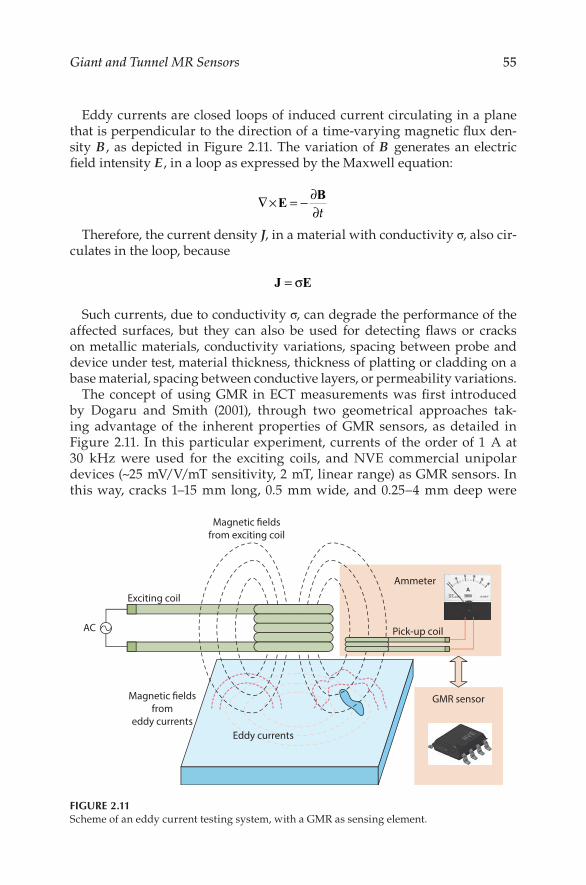
Eddy currents are closed loops of induced current circulating in a plane that is perpendicular to the direction of a time-varying magnetic flux den-sity B , as depicted in Figure 2.11. The variation of B generates an electric field intensity E , in a loop as expressed by the Maxwell equation:
∇× = − ∂∂
E Bt
Therefore, the current density J, in a material with conductivity σ, also cir-culates in the loop, because
J E= σ
Such currents, due to conductivity σ, can degrade the performance of the affected surfaces, but they can also be used for detecting flaws or cracks on metallic materials, conductivity variations, spacing between probe and device under test, material thickness, thickness of platting or cladding on a base material, spacing between conductive layers, or permeability variations.
The concept of using GMR in ECT measurements was first introduced by Dogaru and Smith (2001), through two geometrical approaches tak-ing advantage of the inherent properties of GMR sensors, as detailed in Figure 2.11. In this particular experiment, currents of the order of 1 A at 30 kHz were used for the exciting coils, and NVE commercial unipolar devices (~25 mV/V/mT sensitivity, 2 mT, linear range) as GMR sensors. In this way, cracks 1–15 mm long, 0.5 mm wide, and 0.25–4 mm deep were
Magnetic �eldsfrom exciting coil
Magnetic �eldsfrom
eddy currentsEddy currents
Ammeter
GMR sensor
Pick-up coilAC
Exciting coil
FIGURE 2.11 Scheme of an eddy current testing system, with a GMR as sensing element.
56 Magnetic Sensors and Devices
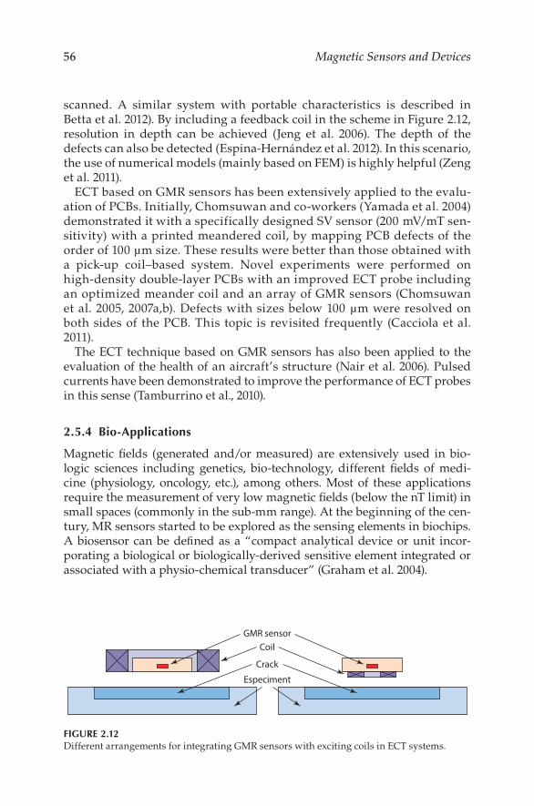
scanned. A similar system with portable characteristics is described in Betta et al. 2012). By including a feedback coil in the scheme in Figure 2.12, resolution in depth can be achieved (Jeng et al. 2006). The depth of the defects can also be detected (Espina-Herná ndez et al. 2012). In this scenario, the use of numerical models (mainly based on FEM) is highly helpful (Zeng et al. 2011).
ECT based on GMR sensors has been extensively applied to the evalu-ation of PCBs. Initially, Chomsuwan and co-workers (Yamada et al. 2004) demonstrated it with a specifically designed SV sensor (200 mV/mT sen-sitivity) with a printed meandered coil, by mapping PCB defects of the order of 100 µ m size. These results were better than those obtained with a pick-up coil–based system. Novel experiments were performed on high-density double-layer PCBs with an improved ECT probe including an optimized meander coil and an array of GMR sensors (Chomsuwan et al. 2005, 2007a,b). Defects with sizes below 100 µ m were resolved on both sides of the PCB. This topic is revisited frequently (Cacciola et al. 2011).
The ECT technique based on GMR sensors has also been applied to the evaluation of the health of an aircraft’ s structure (Nair et al. 2006). Pulsed currents have been demonstrated to improve the performance of ECT probes in this sense (Tamburrino et al., 2010).
2.5.4 Bio‑Applications
Magnetic fields (generated and/or measured) are extensively used in bio-logic sciences including genetics, bio-technology, different fields of medi-cine (physiology, oncology, etc.), among others. Most of these applications require the measurement of very low magnetic fields (below the nT limit) in small spaces (commonly in the sub-mm range). At the beginning of the cen-tury, MR sensors started to be explored as the sensing elements in biochips. A biosensor can be defi ned as a “ compact analytical device or unit incor-porating a biological or biologically-derived sensitive element integrated or associated with a physio-chemical transducer” (Graham et al. 2004).
GMR sensorCoil
Crack
Especiment
FIGURE 2.12 Different arrangements for integrating GMR sensors with exciting coils in ECT systems.
57Giant and Tunnel MR Sensors
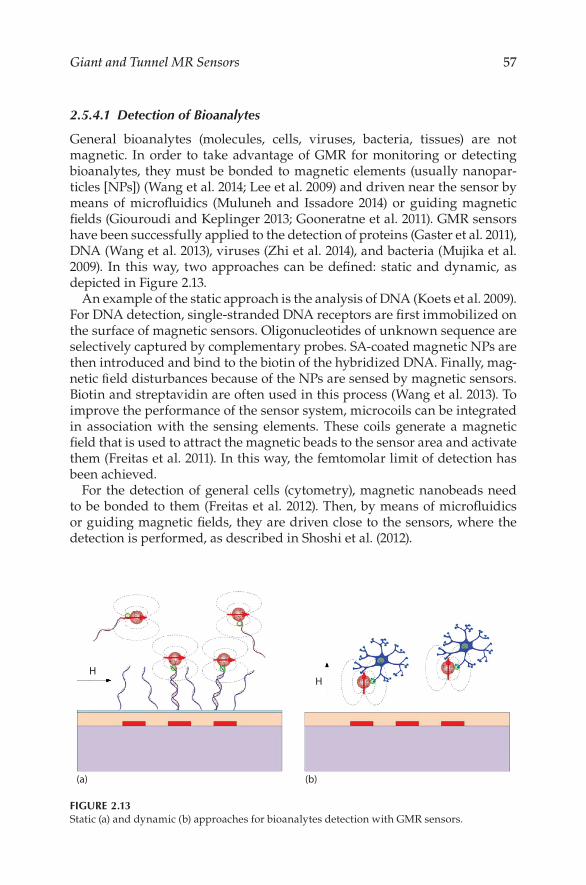
2.5.4.1 Detection of Bioanalytes
General bioanalytes (molecules, cells, viruses, bacteria, tissues) are not magnetic. In order to take advantage of GMR for monitoring or detecting bioanalytes, they must be bonded to magnetic elements (usually nanopar-ticles [NPs]) (Wang et al. 2014; Lee et al. 2009) and driven near the sensor by means of microfluidics (Muluneh and Issadore 2014) or guiding magnetic fields (Giouroudi and Keplinger 2013; Gooneratne et al. 2011). GMR sensors have been successfully applied to the detection of proteins (Gaster et al. 2011), DNA (Wang et al. 2013), viruses (Zhi et al. 2014), and bacteria (Mujika et al. 2009). In this way, two approaches can be defined: static and dynamic, as depicted in Figure 2.13.
An example of the static approach is the analysis of DNA (Koets et al. 2009). For DNA detection, single-stranded DNA receptors are first immobilized on the surface of magnetic sensors. Oligonucleotides of unknown sequence are selectively captured by complementary probes. SA-coated magnetic NPs are then introduced and bind to the biotin of the hybridized DNA. Finally, mag-netic fi eld disturbances because of the NPs are sensed by magnetic sensors. Biotin and streptavidin are often used in this process (Wang et al. 2013). To improve the performance of the sensor system, microcoils can be integrated in association with the sensing elements. These coils generate a magnetic field that is used to attract the magnetic beads to the sensor area and activate them (Freitas et al. 2011). In this way, the femtomolar limit of detection has been achieved.
For the detection of general cells (cytometry), magnetic nanobeads need to be bonded to them (Freitas et al. 2012). Then, by means of microfluidics or guiding magnetic fields, they are driven close to the sensors, where the detection is performed, as described in Shoshi et al. (2012).
H
(a) (b)
H
FIGURE 2.13 Static (a) and dynamic (b) approaches for bioanalytes detection with GMR sensors.
58 Magnetic Sensors and Devices
2.5.4.2 Monitoring of Magnetic Fluids
Fluids incorporating magnetic particles (usually nanobeads) are known as magnetic fluids . They can be made biocompatible for in vivo applications, such as hyperthermia cancer therapy. A magnetic fluid is injected into the affected area and an external ac magnetic flux density is applied to exploit the self-heating properties of the magnetic beads in the fluid. Temperatures in excess of 42° C destroy tumors (Reig et al. 2013). Hence, the accurate estimation of magnetic fluid content density is critical for the success of the treatment. In Mukhopadhyay et al. (2007), a GMR-based needle probe 20 mm long and 310 µ m wide, comprising four SV sensors was analyzed. The needle probe was successfully tested in tumor-simulating cylindrical agar cavities.
2.5.4.3 Biomedical Signal Detection
GMR/TMR-based micromachined probe needles have also been designed for detecting brain activity through the measurement of generated mag-netic fields. After demonstrating the concept (Amaral et al. 2011), MTJ-based microneedles were developed and characterized (Amaral et al. 2013). The associated electronics were also specifically implemented (Costa et al. 2014).
A non-invasive detection system for magnetocardiography applications has also been described by Pannetier-Lecoeur et al. (2010), where a GMR sensor is integrated with a high-temperature superconductor (YBCO).
2.6 Conclusions
GMR/TMR sensors have rapidly passed their initial potentiality in real applications and have become the first option in a huge number of scenar-ios demanding the measurement of low magnetic fields with a high level of integration devices. Complete knowledge of the underlying phenomena has allowed the specific design of different kinds of devices. Their SNR, and subsequent detectivity, make them suitable for most applications in different fields such as bio-technology, microelectronics, and space.
Acknowledgments
The authors are grateful for the very fruitful collaborations that have made possible some of the results presented in this chapter: INESC-MN (Lisboa, Portugal), University of L’ Aquila (Italy), UPC (Barcelona, Spain), and CNM (Barcelona, Spain).
59Giant and Tunnel MR Sensors
References Ač , V. 2008. A study of hysteresis in the GMR layer structures by FEM. Physica B:
Condensed Matter 403 (2–3): 460–63.Amaral, J., S. Cardoso, P. P. Freitas, and A. M. Sebastiã o. 2011. Toward a system to
measure action potential on mice brain slices with local magnetoresistive probes. Journal of Applied Physics 109 (7): 07B308.
Amaral, J., V. Pinto, T. Costa, J. Gaspar, R. Ferreira, E. Paz, S. Cardoso, and P. P. Freitas. 2013. Integration of TMR sensors in silicon microneedles for magnetic mea-surements of neurons. IEEE Transactions on Magnetics 49 (7): 3512–15.
André s, J. P., J. Colino, and J. M. Riveiro. 1999. Enhancement of GMR in as-depos-ited Co-Cu granular films with RF sputtering power. Journal of Magnetism and Magnetic Materials 196–197 (May): 493–94.
Baibich, M. N., J. M. Broto, A. Fert, F. N. Vandau, F. Petroff, P. Eitenne, G. Creuzet, A. Friederich, and J. Chazelas. 1988. Giant magnetoresistance of (001)Fe/(001)Cr magnetic superlattices. Physical Review Letters 61 (21): 2472–75.
Beltran, H., C. Reig, V. Fuster, D. Ramí rez, and M. D. Cubells-Beltrá n. 2007. Modeling of magnetoresistive-based electrical current sensors: A technological approach. IEEE Sensors Journal 7 (11): 1532–37.
Betta, G., L. Ferrigno, and M. Laracca. 2012. GMR-based ECT instrument for detec-tion and characterization of crack on a planar specimen: A hand-held solution. IEEE Transactions on Instrumentation and Measurement 61 (2): 505–12.
Binasch, G., P. Grunberg, F. Saurenbach, and W. Zinn. 1989. Enhanced magneto-resistance in layered magnetic-structures with antiferromagnetic interlayer exchange. Physical Review B 39 (7): 4828–30.
Cacciola, M., G. Megali, D. Pellicanó , and F. C. Morabito. 2011. A GMR–ECT based embedded solution for applications on PCB inspections. Sensors and Actuators A: Physical 167 (1): 25–33.
Cardoso, F. A., H. A. Ferreira, J. P. Conde, V. Chu, P. P. Freitas, D. Vidal, J. Germano, et al. 2006. Diode/magnetic tunnel junction cell for fully scalable matrix-based biochip. Journal of Applied Physics 99 (8): 08B307.
Chen, X., and P. P. Freitas. 2012. Magnetic tunnel junction based on MgO barrier prepared by natural oxidation and direct sputtering deposition. Nano-Micro Letters 4 (1): 25–29.
Chomsuwan, K., S. Yamada, and M. Iwahara. 2007a. Improvement on defect detec-tion performance of PCB inspection based on ECT technique with multi-SV-GMR sensor. IEEE Transactions on Magnetics 43 (6): 2394–96.
Chomsuwan, K., S. Yamada, and M. Iwahara. 2007b. Bare PCB inspection system with SV-GMR sensor eddy-current testing probe. IEEE Sensors Journal 7 (5): 890–96.
Chomsuwan, K., S. Yamada, M. Iwahara, H. Wakiwaka, and S. Shoji. 2005. Application of eddy-current testing technique for high-density double-layer printed circuit board inspection. IEEE Transactions on Magnetics 41 (10): 3619–21.
Costa, T., M. S. Piedade, J. Germano, J. Amaral, and P. P. Freitas. 2014. A neuronal signal detector for biologically generated magnetic fields. IEEE Transactions on Instrumentation and Measurement 63 (5): 1171–80.
Cubells-Beltrá n, M. D., C. Reig, A. De Marcellis, E. Figueras, A. Yú fera, B. Zadov, E. Paperno, S. Cardoso, and P. P. Freitas. 2014. Monolithic integration of giant magnetoresistance (GMR) devices onto standard processed CMOS dies. Microelectronics Journal 45 (6): 702–7.
60 Magnetic Sensors and Devices
Cubells-Beltrá n, M.-D., C. Reig, J. Martos, J. Torres, and J. Soret. 2011. Limitations of magnetoresistive current sensors in industrial electronics applications. International Review of Electrical Engineering (IREE) 6 (1): 423–29.
Cubells-Beltrá n, M. D., C. Reig, D. R. Muñ oz, S. I. P. C. de Freitas, and P. J. P. De Freitas. 2009. Full Wheatstone bridge spin-valve based sensors for IC currents monitor-ing. IEEE Sensors Journal 9 (12): 1756–62.
Dí az-Michelena, M. 2009. Small magnetic sensors for space applications. Sensors (Basel, Switzerland) 9 (4): 2271–88.
Dogaru, T., and S. T. Smith. 2001. Giant magnetoresistance-based eddy-current sen-sor. IEEE Transactions on Magnetics 37 (5): 3831–38.
Espina-Herná ndez, J. H., E. Ramí rez-Pacheco, F. Caleyo, J. A. Pé rez-Benitez, and J. M. Hallen. 2012. Rapid estimation of artificial near-side crack dimensions in aluminium using a GMR-based eddy current sensor. NDT & E International 51 (October): 94–100.
Ferreira, R., P. Wisniowski, P. P. Freitas, J. Langer, B. Ocker, and W. Maass. 2006. Tuning of MgO barrier magnetic tunnel junction bias current for picotesla magnetic field detection. Journal of Applied Physics 99 (8): 08K706.
Freitas, P. P., F. A. Cardoso, V. C. Martins, S. A. M. Martins, J. Loureiro, J. Amaral, R. C. Chaves, et al. 2012. Spintronic platforms for biomedical applications. Lab on a Chip 12 (3): 546–57.
Freitas, P. P., S. Cardoso, R. Ferreira, V. C. Martins, A. Guedes, F. A. Cardoso, J. Loureiro, R. Macedo, R. C. Chaves, and J. Amaral. 2011. Optimization and inte-gration of magnetoresistive sensors. SPIN 01 (01): 71–91.
Freitas, P. P., R. Ferreira, S. Cardoso, and F. Cardoso. 2007. Magnetoresistive sensors. Journal of Physics: Condensed Matter 19 (16). IOP Publishing: 165221.
Gaster, R. S, L. Xu, S-J. Han, R. J. Wilson, D. A. Hall, S. J. Osterfeld, H. Yu, and S. X. Wang. 2011. Quantification of protein interactions and solution transport using high-density GMR sensor arrays. Nature Nanotechnology 6 (5): 314–20.
Giouroudi, I., and F. Keplinger. 2013. Microfluidic biosensing systems using mag-netic nanoparticles. International Journal of Molecular Sciences 14 (9): 18535–56.
Gooneratne, C. P., C. Liang, and J. Kosel. 2011. A planar conducting microstructure to guide and confine magnetic beads to a sensing zone. Microelectronic Engineering 88 (8): 1757–60.
Graham, D. L., H. A. Ferreira, and P. P. Freitas. 2004. Magnetoresistive-based biosen-sors and biochips. Trends in Biotechnology 22 (9): 455–62.
Guerrero, R., M. Pannetier-Lecoeur, C. Fermon, S. Cardoso, R. Ferreira, and P. P. Freitas. 2009. Low frequency noise in arrays of magnetic tunnel junctions con-nected in series and parallel. Journal of Applied Physics 105 (11): 113922.
Hall, D. A., R. S. Gaster, K. Makinwa, S. X. Wang, and B. Murmann. 2013. A 256 pixel magnetoresistive biosensor microarray in 0.18μ m CMOS. IEEE Journal of Solid-State Circuits 48 (5): 1290–1301.
Han, J., J. Hu, Y. Ouyang, S. X. Wang, and J. He. 2015. Hysteretic modeling of output characteristics of giant magnetoresistive current sensors. IEEE Transactions on Industrial Electronics 62 (1): 516–24.
Hankard, F., J. Gattacceca, C. Fermon, M. Pannetier-Lecoeur, B. Langlais, Y. Quesnel, P. Rochette, and S. A. McEnroe. 2009. Magnetic field microscopy of rock samples using a giant magnetoresistance-based scanning magnetometer. Geochemistry, Geophysics, Geosystems 10: Q10Y06.
61Giant and Tunnel MR Sensors
He, H., K. Zhernenkov, M. Vadala , N. Akdogan, D. Gorkov, R. M. Abrudan, B. P. Toperverg, H. Zabel, H. Kubota, and S. Yuasa. 2010. The effect of annealing on the junction profile of CoFeB/MgO tunnel junctions. Journal of Applied Physics 108 (6): 063922.
Hirota, E., H. Sakakima, and K. Inomata. 2002. Giant Magneto-Resistance Devices . Vol. 40. Springer Series in Surface Sciences. Berlin: Springer. doi:10.1007/978-3-662-04777-4.
Hooge, F. N. 1976. 1/f noise. Physica B+C 83 (1): 14–23.Jedlicska, I., R. Weiss, and R. Weigel. 2010. Linearizing the output characteristic
of GMR current sensors through hysteresis modeling. IEEE Transactions on Industrial Electronics 57 (5): 1728–34.
Jeng, J.-T., G-S. Lee, W-C. Liao, and C-L. Shu. 2006. Depth-resolved eddy-current detection with GMR magnetometer. Journal of Magnetism and Magnetic Materials 304 (1): e470–73.
Johnson, J. B. 1928. Thermal agitation of electricity in conductors. Physical Review 32 (1): 97–109.
Koets, M., T. van der Wijk, J. T. W. M. van Eemeren, A. van Amerongen, and M. W. J. Prins. 2009. Rapid DNA multi-analyte immunoassay on a magneto-resistance biosensor. Biosensors and Bioelectronics 24 (7): 1893–98.
Ku, W., P. P. Freitas, P. Compadrinho, and J. Barata. 2000. Precision X-Y robotic object handling using a dual GMR bridge sensor. IEEE Transactions on Magnetics 36 (5): 2782–84.
Le, P., K., H. Boeve, F. Vanhelmont, T. Ikkink, and W. Talen. 2005. Geometry opti-mization of TMR current sensors for on-chip IC testing. IEEE Transactions on Magnetics 41 (10): 3685–87.
Lee, K., S. Lee, B. K. Cho, K-S. Kim, and B. Kim. 2009. The limit of detection of giant magnetoresistive (GMR) sensors for bio-applications. Journal of the Korean Physical Society 55 (1): 193–96.
Lenssen, K.-M. H., G. H. J. Somers, and J. B. A. D. van Zon. 2002. Magnetoresistive sensors for string instruments. Journal of Applied Physics 91 (10): 7777.
Liu, S., Q. Huang, Y. Li, and W. Zhen. 2012. Experimental research on hysteresis effects in GMR sensors for analog measurement applications. Sensors and Actuators A: Physical 182 (August): 72–81.
Lopez-Martin, A. J., and A. Carlosena. 2009. Performance tradeoffs of three novel GMR contactless angle detectors. IEEE Sensors Journal 9 (3): 191–98.
Madrenas, J., M.-D. Cubells-Beltrá n, B. Zadov, S. Cardoso, C. Reig, P. P. Freitas, E. Paperno, and A. De Marcellis. 2014. Quasi-digital front-ends for current mea-surement in integrated circuits with giant magnetoresistance technology. IET Circuits, Devices {&} Systems 8 (4): 291–300.
Mujika, M., S. Arana, E. Castañ o, M. Tijero, R. Vilares, J. M. Ruano-Ló pez, A. Cruz, L. Sainz, and J. Berganza. 2009. Magnetoresistive immunosensor for the detec-tion of Escherichia coli O157:H7 including a microfluidic network. Biosensors & Bioelectronics 24 (5): 1253–58.
Mukhopadhyay, S. C., K. Chomsuwan, C. P. Gooneratne, and S. Yamada. 2007. A novel needle-type SV-GMR sensor for biomedical applications. IEEE Sensors Journal 7 (3): 401–8.
Muluneh, M., and D. Issadore. 2014. A multi-scale PDMS fabrication strategy to bridge the size mismatch between integrated circuits and microfluidics. Lab on a Chip 14 (23): 4552–58.
62 Magnetic Sensors and Devices
Nair, N. V., V. R. Melapudi, H. R. Jimenez, X. Liu, Y. Deng, Z. Zeng, L. Udpa, T. J. Moran, and S. S. Udpa. 2006. A GMR-based eddy current system for NDE of aircraft structures. IEEE Transactions on Magnetics 42 (10): 3312–14.
Nyquist, H. 1928. Thermal agitation of electric charge in conductors. Physical Review 32 (1): 110–13.
Pannetier-Lecoeur, M., C. Fermon, A. de Vismes, E. Kerr, and L. Vieux-Rochaz. 2007. Low noise magnetoresistive sensors for current measurement and compasses. Journal of Magnetism and Magnetic Materials 316 (2): e246–48.
Pannetier-Lecoeur, M., C. Fermon, H. Dyvorne, J. F. Jacquinot, H. Polovy, and A. L. Walliang. 2010. Magnetoresistive-superconducting mixed sensors for bio-magnetic applications. Journal of Magnetism and Magnetic Materials 322 (9–12): 1647–50.
Pelegrí Sebastiá , J., J. Alberola Lluch, and J. Rafael Lajara Vizcaí no. 2007. Signal condi-tioning for GMR magnetic sensors applied to traffic speed monitoring. Sensors and Actuators A: Physical 137 (2): 230–35.
Pelegri Sebastia, J., D. R. Munoz, and P. J. P. de Freitas. 2004. A novel spin-valve bridge sensor for current sensing. IEEE Transactions on Instrumentation and Measurement 53 (3): 877–80.
Peñ a, V., Z. Sefrioui, D. Arias, C. Leon, J. Santamaria, J. L. Martinez, S. G. E. Te Velthuis, and A. Hoffmann. 2005. Giant magnetoresistance in ferromagnet/superconductor superlattices. Physical Review Letters 94 (5): 057002.
Pullini, D., D. Busquets, A. Ruotolo, G. Innocenti, and V. Amigó . 2007. Insights into pulsed electrodeposition of GMR multilayered nanowires. Journal of Magnetism and Magnetic Materials 316 (2): e242–45.
Ramírez Muñoz, D., J. Sa nchez Moreno, S. Casans Berga, E. Castro Montero, C. Reig Escriva , and A. Edith Navarro Anto n. 2006. Temperature compensation of Wheatstone bridge magnetoresistive sensors based on generalized impedance con-verter with input reference current. Review of Scientific Instruments 77 (10): 105102.
Ranchal, R., M. Torija, E. Ló pez, M. C. Sá nchez, C. Aroca, and P. Sá nchez. 2002. The influence of anisotropy on the magnetoresistance of permalloy-copper-permal-loy thin films. Nanotechnology 13 (3): 392–97.
Reig, C., S. Cardoso, and S. Mukhopadhyay. 2013. Giant Magnetoresistance (GMR) Sensors: From Basis to State-of-the-Art Applications . Berlin: Springer.
Reig, C., M.-D. Cubells-Beltran, D. Ramirez, S. Cardoso, and P.P. Freitas. 2008. Electrical isolators based on tunneling magnetoresistance technology. IEEE Transactions on Magnetics 44 (11): 4011–14.
Reig, C., M.-D. Cubells-Beltran, and D. Ramí rez Muñ oz. 2009. Magnetic field sensors based on giant magnetoresistance (GMR) technology: Applications in electrical current sensing. Sensors (Basel, Switzerland) 9 (10): 7919–42.
Reig, C., D. Ramirez, H. H. Li, and P. P. Freitas. 2005. Low-current sensing with specular spin valve structures. IEE Proceedings: Circuits, Devices and Systems 152 (4): 307–11.
Reig, C., D. Ramí rez, F. Silva, J. Bernardo, P. Freitas, D. Ramı rez, F. Silva, J. Bernardo, and P. Freitas. 2004. Design, fabrication, and analysis of a spin-valve based cur-rent sensor. Sensors and Actuators, A: Physical 115: 259–66.
Renhart, W., M. Bellina, C. Magele, and A. Kö stinger. 2011. Hidden metallic object localization by using giant magnetic resistor sensors. COMPEL: The International Journal for Computation and Mathematics in Electrical and Electronic Engineering 30 (6): 1927–37.
63Giant and Tunnel MR Sensors
Ripka, P., and M. Janosek. 2010. Advances in magnetic field sensors. IEEE Sensors Journal 10 (6): 1108–16.
Ripka, P., M. Tondra, J. Stokes, and R. Beech. 1999. AC-driven AMR and GMR magne-toresistors. Sensors and Actuators A: Physical 76 (1–3): 225–30.
Roldá n, A., C. Reig, M. D. Cubells-Beltrá n, J. B. Roldá n, D. Ramí rez, S. Cardoso, and P. P. Freitas. 2010a. Analytical compact modeling of GMR based current sensors: Application to power measurement at the IC level. Solid-State Electronics 54 (12): 1606–12.
Roldá n, A., C. Reig, M. D. D. Cubells-Beltrá n, J. B. B. Roldá n, D. Ramí rez, S. Cardoso, and P. P. P. Freitas. 2010b. Analytical compact modeling of GMR based cur-rent sensors: Application to power measurement at the IC level. Solid-State Electronics 54 (12): 1606–12.
Sanchez, J., D. Ramirez, S. I. Ravelo, A. Lopes, S. Cardoso, R. Ferreira, and P. P. Freitas. 2012. Electrical characterization of a magnetic tunnel junction current sensor for industrial applications. IEEE Transactions on Magnetics 48 (11): 2823–26.
Sá nchez Moreno, J., D. Ramí rez Muñ oz, S. Cardoso, S. Casans Berga, A. E. Navarro Antó n, and P. J. Peixeiro de Freitas. 2011. A non-invasive thermal drift com-pensation technique applied to a spin-valve magnetoresistive current sensor. Sensors (Basel, Switzerland) 11 (3): 2447–58.
Sebastia, J. P., J. Alberola Lluch, J. R. Lajara Vizcaino, and J. Santiso Bellon. 2009. Vibration detector based on GMR sensors. IEEE Transactions on Instrumentation and Measurement 58 (3): 707–12.
Shoshi, A., J. Schotter, P. Schroeder, M. Milnera, P. Ertl, V. Charwat, M. Purtscher, et al. 2012. Magnetoresistive-based real-time cell phagocytosis monitoring. Biosensors & Bioelectronics 36 (1): 116–22.
Singh, R. P., and A. M. Khambadkone. 2008. Giant magneto resistive (GMR) effect based current sensing technique for low voltage/high current voltage regulator modules. IEEE Transactions on Power Electronics 23 (2): 915–25.
Singh, R. P., and A. M. Khambadkone. 2014. A giant magneto resistive (GMR) effect based current sensor with a toroidal magnetic core as flux concentrator and closed-loop configuration. IEEE Transactions on Applied Superconductivity 24 (3): 1–5.
Stutzke, N. A., S. E. Russek, D. P. Pappas, and M. Tondra. 2005. Low-frequency noise measurements on commercial magnetoresistive magnetic field sensors. Journal of Applied Physics 97 (10): 10Q107.
Tamburrino, A., L. Udpa, and S. S. Udpa. 2010. Pulsed eddy-current based giant mag-netoresistive system for the inspection of aircraft structures. IEEE Transactions on Magnetics 46 (3): 910–17.
Thompson, S. M. 2008. The discovery, development and future of GMR: The Nobel Prize 2007. Journal of Physics D: Applied Physics 41 (9): 093001.
Tian, G. Y., A. Al-Qubaa, and J. Wilson. 2012. Design of an electromagnetic imaging system for weapon detection based on GMR sensor arrays. Sensors and Actuators A: Physical 174 (February): 75–84.
Vieth, M., W. Clemens, H. van den Berg, G. Rupp, J. Wecker, and M. Kroeker. 2000. Contactless current detection with GMR sensors based on an artificial antifer-romagnet (AAF) subsystem. Sensors and Actuators A: Physical 81 (1–3): 44–48.
Vopalensky, M., and A. Platil. 2013. Temperature drift of offset and sensitivity in full-bridge magnetoresistive sensors. IEEE Transactions on Magnetics 49 (1): 136–39.
64 Magnetic Sensors and Devices
Vopá lenský , M., P. Ripka, J. Kubı k, and M. Tondra. 2004. Improved GMR sensor bias-ing design. Sensors and Actuators A: Physical 110 (1–3): 254–58.
Wang, W., Y. Wang, L. Tu, Y. Feng, T. Klein, and J.-P. Wang. 2014. Magnetoresistive performance and comparison of supermagnetic nanoparticles on giant mag-netoresistive sensor-based detection system. Scientific Reports 4 (January): 5716.
Wang, W., Y. Wang, L. Tu, T. Klein, Y. Feng, and J.-P. Wang. 2013. Surface modification for protein and DNA immobilization onto GMR biosensor. IEEE Transactions on Magnetics 49 (1): 296–99.
Yamada, S., K. Chomsuwan, Y. Fukuda, M. Iwahara, H. Wakiwaka, and S. Shoji. 2004. Eddy-current testing probe with spin-valve type GMR sensor for printed cir-cuit board inspection. IEEE Transactions on Magnetics 40 (4): 2676–78.
Zeng, Z., Y. Deng, X. Liu, L. Udpa, S. S. Udpa, B. E. C. Koltenbah, R. H. Bossi, and G. Steffes. 2011. EC-GMR data analysis for inspection of multilayer airframe struc-tures. IEEE Transactions on Magnetics 47 (12): 4745–52.
Zhi, X., M. Deng, H. Yang, G. Gao, K. Wang, H. Fu, Y. Zhang, D. Chen, and D. Cui. 2014. A novel HBV genotypes detecting system combined with microfluidic chip, loop-mediated isothermal amplification and GMR sensors. Biosensors & Bioelectronics 54 (April): 372–77.
Ziegler, S., R. C. Woodward, H. Ho-Ching Iu, and L. J. Borle. 2009. Current sensing techniques: A review. IEEE Sensors Journal 9 (4): 354–76.
Ziese, M., and M. J. Thornton. 2001. Spin Electronics . Lecture Notes in Physics . Berlin: Springer-Verlag.


![Covert Channels Using Mobile Device’s Magnetic Field Sensors · magnetic sensors, also called magnetometers. As the in-dustrial cost of magnetic sensors is very low [14], they are](https://img.pdfslide.us/doc/110x75/5f484cb0c102e5416e04ffc3/covert-channels-using-mobile-deviceas-magnetic-field-sensors-magnetic-sensors.jpg)