Embed Size (px)
Citation preview
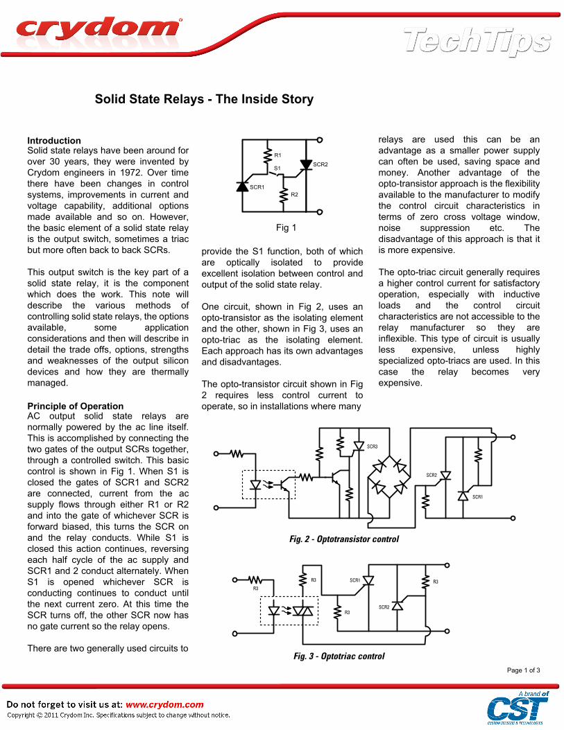
Fig 1
R1
R2SCR1
SCR2S1
Solid State Relays - The Inside Story
Page 1 of 3
Introduction
Fig. 2 - Optotransistor control
SCR1
SCR2
SCR3
SCR1
SCR2
R3
R3
R3
R3
Fig. 3 - Optotriac control
Solid state relays have been around for over 30 years, they were invented by Crydom engineers in 1972. Over time there have been changes in control systems, improvements in current and voltage capability, additional options made available and so on. However, the basic element of a solid state relay is the output switch, sometimes a triac but more often back to back SCRs.
This output switch is the key part of a solid state relay, it is the component which does the work. This note will describe the various methods of controlling solid state relays, the options available, some application considerations and then will describe in detail the trade offs, options, strengths and weaknesses of the output silicon devices and how they are thermally managed.
Principle of OperationAC output solid state relays are normally powered by the ac line itself. This is accomplished by connecting the two gates of the output SCRs together, through a controlled switch. This basic control is shown in Fig 1. When S1 is closed the gates of SCR1 and SCR2 are connected, current from the ac supply flows through either R1 or R2 and into the gate of whichever SCR is forward biased, this turns the SCR on and the relay conducts. While S1 is closed this action continues, reversing each half cycle of the ac supply and SCR1 and 2 conduct alternately. When S1 is opened whichever SCR is conducting continues to conduct until the next current zero. At this time the SCR turns off, the other SCR now has no gate current so the relay opens.
There are two generally used circuits to
provide the S1 function, both of which are optically isolated to provide excellent isolation between control and output of the solid state relay.
One circuit, shown in Fig 2, uses an opto-transistor as the isolating element and the other, shown in Fig 3, uses an opto-triac as the isolating element. Each approach has its own advantages and disadvantages.
The opto-transistor circuit shown in Fig 2 requires less control current to operate, so in installations where many
relays are used this can be an advantage as a smaller power supply can often be used, saving space and money. Another advantage of the opto-transistor approach is the flexibility available to the manufacturer to modify the control circuit characteristics in terms of zero cross voltage window, noise suppression etc. The disadvantage of this approach is that it is more expensive. The opto-triac circuit generally requires a higher control current for satisfactory operation, especially with inductive loads and the control circuit characteristics are not accessible to the relay manufacturer so they are inflexible. This type of circuit is usually less expensive, unless highly specialized opto-triacs are used. In this case the relay becomes very expensive.
Page 2 of 3
Application Considerations
Solid state relays can be supplied with either a zero voltage turn on feature or an instantaneous turn on. Depending on the application the designer will decide which is best for his end use. With a modified version of the opto-transistor circuit of Fig 2 a normally closed solid state relay can be designed.
Solid state relays can be either ac or dc voltage controlled, for ac control the ac signal is rectified and filtered to provide dc to the opto-transistor or opto-triac LED. Obviously the ac control versions can also be dc controlled, just one half of the rectifier is used.
Different applications require different solid state relay characteristics. The two turn on methods, zero cross or instantaneous would appear to have specific application areas. However, as is normally the case there are no absolute rules for when either of these two turn on methods should be used.
If the load requires proportional control every half cycle (such as incandescent lamp dimming, low thermal mass temperature control) then the instantaneous turn on type has to be used. For high thermal mass loads then a zero cross relay with complete cycles of conduction and non-conduction is usually the preferred method of temperature control.
For inductive loads it has generally been proposed that a zero cross turn on relay is used. Depending on the application and the power factor, it may be more suitable to use an instantaneous turn on relay for inductive loads. There is no standard rule but in general an instantaneous turn on relay is the preferred type for inductive loads.
Key Elements of Solid State RelaysAs discussed earlier there are a number
of ways to control the output of a solid state relay but the key phrase is “the output of a solid state relay”.
In most cases Crydom uses back to back SCRs as the output elements of its ac output solid state relays. There are performance advantages associated with the back to back SCR configuration compared with triac outputs. The major benefit is dv/dt, triacs have a severe dv/dt limitation when they are turning off, the commutating dv/dt of a triac is normally in the 5 to 10 V/microsecond range. Back to back SCRs do not have this limitation, there is no commutating dv/dt associated with this arrangement, just critical dv/dt, which is greater than 500 V/microsecond. There are thermal benefits to using two output elements (back to back SCR) compared with a single element (triac) as the heat dissipated is spread over a wider area of the ceramic insulator. Although the aluminum oxide ceramic substrate, used to isolate the solid state relay from the base plate, is a good compromise, as a thermal conductor it has its limitations. The ceramic substrate does not conduct heat laterally very efficiently, so by separating the heat source into two elements, more of the substrate is used to conduct the heat vertically through the ceramic. Additionally the two SCRs are attached to their own, substantial, copper leadframes which further help to spread the heat over a larger area of the ceramic substrate. Even with the extensive use of copper leadframes to spread the heat, the ceramic substrate is the dominant source of thermal impedance, contributing approximately 50% to the total thermal impedance of the relay, from SCR chip to relay baseplate.
If the relay is subjected to surge currents then the back to back SCR approach is preferred because each
element is isolated from its partner both thermally and electrically. This is not the case for a single element triac output.
Even the use of SCRs as the output element of a solid state relay is not a straightforward decision. Economics is a strong consideration when the manufacturer is deciding what size and type of SCR to use. The output silicon of the relay is a major component of the relay, certainly the control circuit determines turn on, turn off characteristics but it is the output silicon switch, which is the key to performance.
Obviously the smaller the SCR chip the lower the cost but this also results in lower performance – surge (or overload) current is reduced, power dissipation is increased and thermal impedance is increased. Of these maybe reducing the thickness of the silicon can marginally increase surge current, the forward voltage drop and so power dissipation will also be reduced. However, using thinner silicon is not as easy a solution as it may appear. For the SCR chip manufacturer there will be yield penalties due to increased wafer breakage and lower blocking voltage yield, so the cost will be higher. The blocking voltage of the thinner SCR chips will probably be lower so making the final solid state relay significantly more susceptible to transient overvoltage damage, especially if the thickness is reduced to the point where the SCR breakover is not an avalanche breakover but punch through breakdown. If the silicon is susceptible to punch through breakdown then any overvoltage will destroy the SCR chip in question, where with an avalanche breakdown the SCR will normally self fire, conduct for the remainder of the half cycle and then return to its normal blocking condition, undamaged.
If thinner silicon has disadvantages then perhaps thicker silicon chips
Page 3 of 3
should be considered. Thicker chips will generally be more rugged relative to overvoltage transients and will normally have a higher blocking voltage rating. The forward voltage drop will be higher resulting in higher power dissipation and lower surge current capability. For the silicon chip manufacturer the overall yield will be higher due to less wafer breakage and higher useful voltage yield, so the chip cost will be lower.
ConclusionTo maximize performance while using economically priced SCR die solid state relay manufacturers work very closely with their power semiconductor suppliers.


![[ 3000 Series Time Delay Relays and Measuring Relays ... · [ 3000 Series Time Delay Relays and Measuring Relays ] ... Measuring Relays ] • Time Delay Relays ... Dear Reader, Dear](https://img.pdfslide.us/doc/110x75/5b85683b7f8b9aec488e43dd/-3000-series-time-delay-relays-and-measuring-relays-3000-series-time.jpg)