Embed Size (px)
Citation preview
Solid-State Electronics Chap. 6
Instructor: Pei-Wen LiDept. of E. E. NCU
1
Chap 6. Nonequilibrium Excess Carriers in Semiconductor
Carrier Generation and Recombination Continuity Equation Ambipolar Transport Quasi-Fermi Energy Levels Excess-Carrier Lifertime Surface Effects

Solid-State Electronics Chap. 6
Instructor: Pei-Wen LiDept. of E. E. NCU
2
Nonequilibrium
When a voltage is applied or a current exists in a semiconductor device, the semiconductor is operating under nonequilibrium conditions.
Excess electrons/holes in the conduction/valence bands may be generated and recombined in addition to the thermal equilibrium concentrations if an external excitation is applied to the semiconductor.
Examples:
1. A sudden increase in temperature will increase the thermal generation rate of electrons and holes so that their concentration will change with time until new equilibrium reaches.
2. A light illumination on the semiconductor (a flux of photons) can also generate electron-hole pairs, creating a nonequilibrium condition.
Solid-State Electronics Chap. 6
Instructor: Pei-Wen LiDept. of E. E. NCU
3
Generation and Recombination
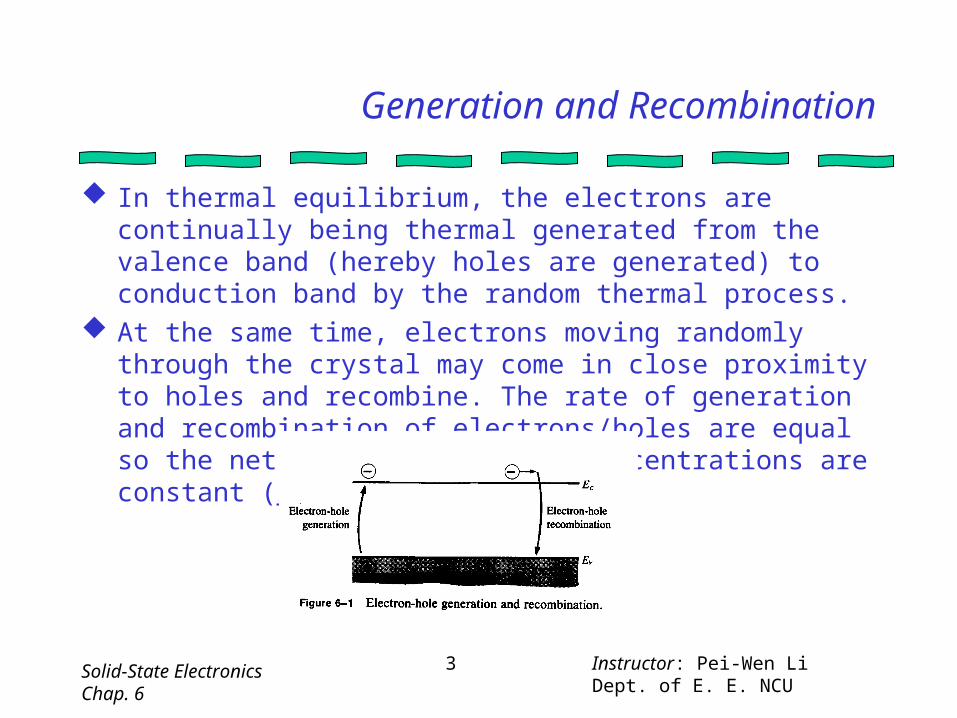
In thermal equilibrium, the electrons are continually being thermal generated from the valence band (hereby holes are generated) to conduction band by the random thermal process.
At the same time, electrons moving randomly through the crystal may come in close proximity to holes and recombine. The rate of generation and recombination of electrons/holes are equal so the net electron and hole concentrations are constant (independent of time).
Solid-State Electronics Chap. 6
Instructor: Pei-Wen LiDept. of E. E. NCU
4
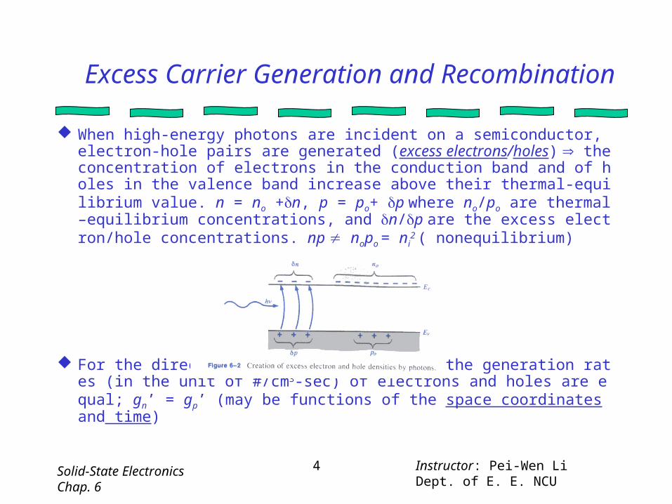
Excess Carrier Generation and Recombination
When high-energy photons are incident on a semiconductor, electron-hole pairs are generated (excess electrons/holes) the concentration of electrons in the conduction band and of holes in the valence band increase above their thermal-equilibrium value. n = no +n, p = po+ p where no/po are thermal–equilibrium concentrations, and n/p are the excess electron/hole concentrations. np nopo = ni
2 ( nonequilibrium)
For the direct band-to-band generation, the generation rates (in the unit of #/cm3-sec) of electrons and holes are equal; gn’ = gp’ (may be functions of the space coordinates and time)

Solid-State Electronics Chap. 6
Instructor: Pei-Wen LiDept. of E. E. NCU
5
Excess Carrier Generation and Recombination
An electron in conduction band may “fall down” into the valence band and leads to the excess electron-hole recombination process.
Since the excess electrons and holes recombine in pairs so the recombination rates for excess electrons and holes are equal, Rn’ = Rp’. (in the unit of #/cm3-sec). n(t) = p(t)
The direct band-to-band recombination is spontaneous, thus the probability of an electron and hole recombination is constant with time.
Rn’ = Rp’ the electron and hole concentration.

Solid-State Electronics Chap. 6
Instructor: Pei-Wen LiDept. of E. E. NCU
6
Recombination Process
Band-to-Band: direct thermal recombination. This process is typically radiative, with the excess energy releasedduring the process going into the production of a photon (light)
R-G Center: Induced by certain impurity atoms or crystal defects. Electron and hole are attracted to the R-G center and lead to the annihilation of the electron-hole pair. Or a carrier is first captured at the R-G
site and then makes an annihilating transition to the opposite carrier band. This process is indirect thermal recombination (nonradiativ
e). Thermal energy (heat) is released during the process (lattice vibrations, phonons are produced)

Solid-State Electronics Chap. 6
Instructor: Pei-Wen LiDept. of E. E. NCU
7
Recombination Process
Recombination via Shallow Levels:—induced by donor or acceptor sites. At RT, if an electron is captured at a donor site,however, it has a high probability of being re-emitted into the conduction band before completing the recombination process. Therefore, the probability of recombination via shallow levels is quite low at RT. It should be noted that the probability of observing shallow-level processes increases with decreasing system temperature.
Recombination involving Excitons:It is possible for an electron and a hole to become boundtogether into a hydrogen-atom-like arrangement which moves as a unit in response to applied forces. This coupled e-h pair is called an “exciton”. The formation of an exciton can be viewed as introducing a temporary level into the bandgap slightly above or below the band edge.
Solid-State Electronics Chap. 6
Instructor: Pei-Wen LiDept. of E. E. NCU
8
Recombination Process
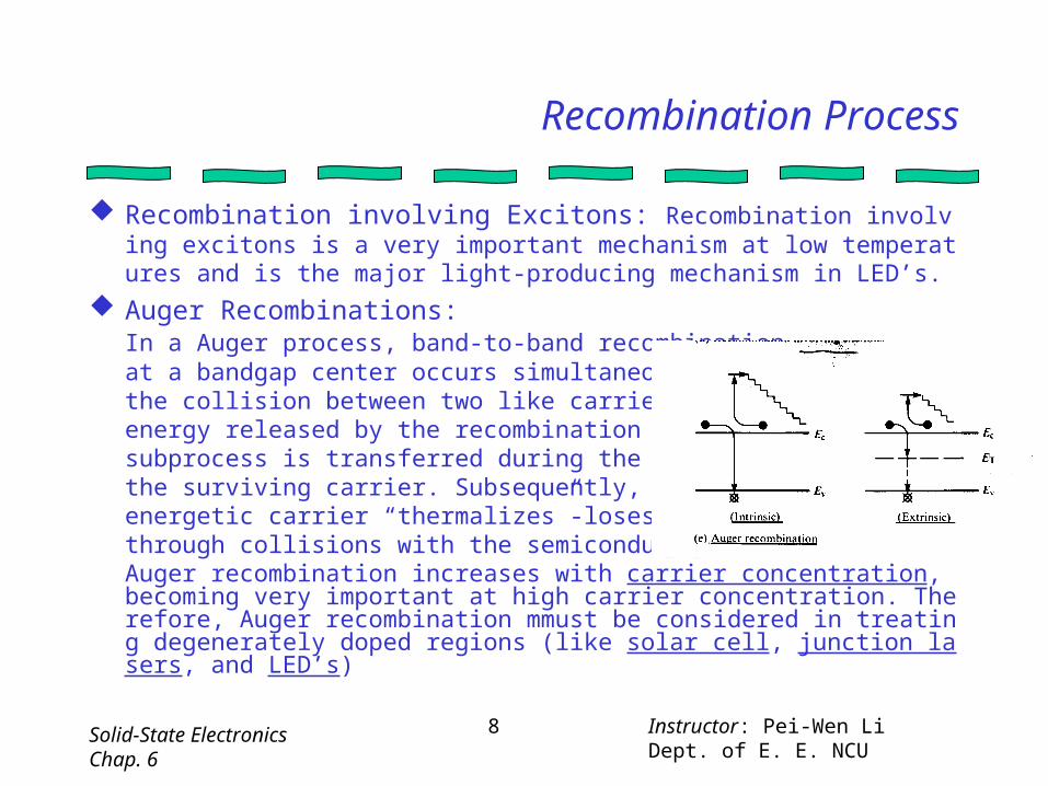
Recombination involving Excitons: Recombination involving excitons is a very important mechanism at low temperatures and is the major light-producing mechanism in LED’s.
Auger Recombinations:In a Auger process, band-to-band recombinationat a bandgap center occurs simultaneously with the collision between two like carriers. The energy released by the recombination or trappingsubprocess is transferred during the collision to the surviving carrier. Subsequently, this high energetic carrier “thermalizes”-loses energy through collisions with the semiconductor lattice.Auger recombination increases with carrier concentration, becoming very important at high carrier concentration. Therefore, Auger recombination mmust be considered in treating degenerately doped regions (like solar cell, junction lasers, and LED’s)

Solid-State Electronics Chap. 6
Instructor: Pei-Wen LiDept. of E. E. NCU
9
Generation Process
Band-to-Band generation:
R-G center generation:
Photoemission from band gap centers:

Solid-State Electronics Chap. 6
Instructor: Pei-Wen LiDept. of E. E. NCU
10
Generation Process
Impact-Ionization:An e-h pair is produced as a result of the energy released when a highly energetic carrier collides with the crystal lattice. The generation of carriers through impact ionizationroutinely occurs in the high e-filed regions of devices and is responsible for the avalanche breakdown in pn junctions.
Solid-State Electronics Chap. 6
Instructor: Pei-Wen LiDept. of E. E. NCU
11
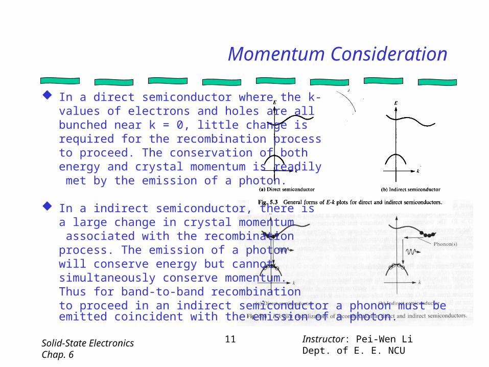
Momentum Consideration
In a direct semiconductor where the k-values of electrons and holes are all bunched near k = 0, little change is required for the recombination process to proceed. The conservation of both energy and crystal momentum is readily met by the emission of a photon.
In a indirect semiconductor, there isa large change in crystal momentum associated with the recombination process. The emission of a photon will conserve energy but cannot simultaneously conserve momentum. Thus for band-to-band recombination to proceed in an indirect semiconductor a phonon must be emitted coincident with the emission of a photon.
Solid-State Electronics Chap. 6
Instructor: Pei-Wen LiDept. of E. E. NCU
12
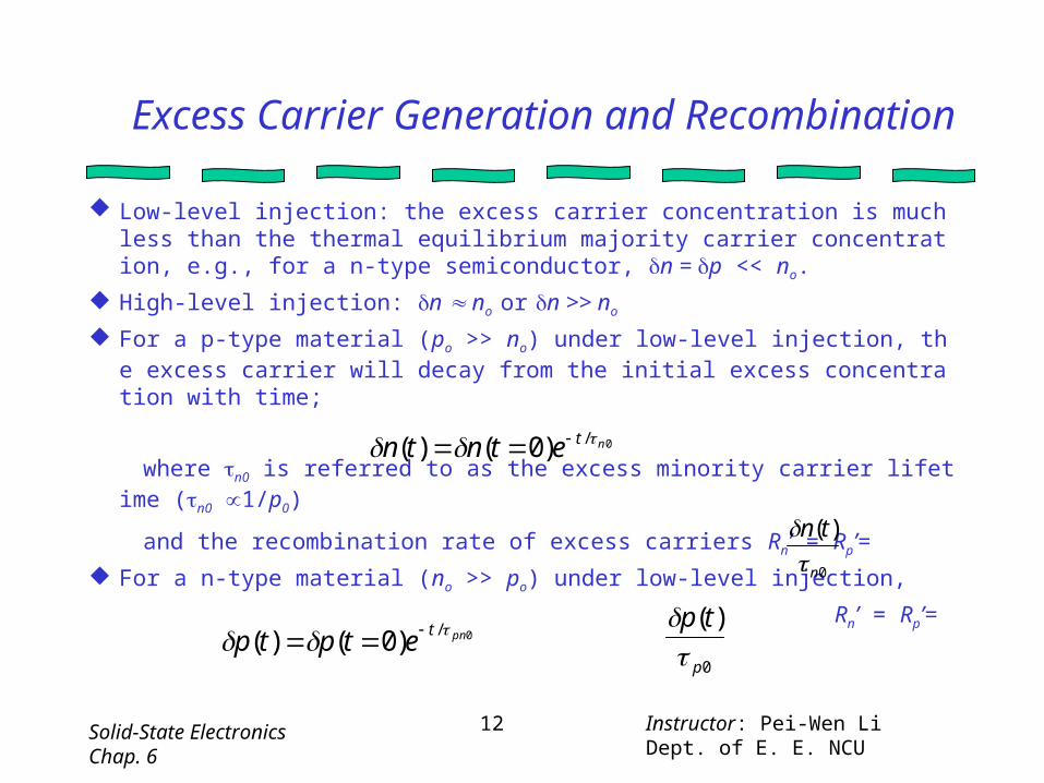
Excess Carrier Generation and Recombination
Low-level injection: the excess carrier concentration is much less than the thermal equilibrium majority carrier concentration, e.g., for a n-type semiconductor, n = p << no.
High-level injection: n no or n >> no
For a p-type material (po >> no) under low-level injection, the excess carrier will decay from the initial excess concentration with time;
where n0 is referred to as the excess minority carrier lifetime (n0 1/p0)
and the recombination rate of excess carriers Rn’ = Rp’=
For a n-type material (no >> po) under low-level injection,
Rn’ = Rp’=
0
)(
n
tn
0/)0()( ntetntn
0/)0()( pntetptp 0
)(
p
tp
Solid-State Electronics Chap. 6
Instructor: Pei-Wen LiDept. of E. E. NCU
13
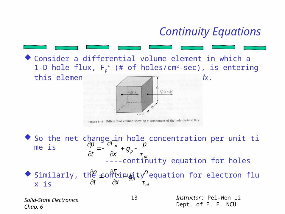
Continuity Equations
Consider a differential volume element in which a 1-D hole flux, Fp+
(# of holes/cm2-sec), is entering this element at x and is leaving at x+dx.
So the net change in hole concentration per unit time is
----continuity equation for holes
Similarly, the continuity equation for electron flux is
ptp
p pg
x
F
t
p
ntn
n ng
x
F
t
n

Solid-State Electronics Chap. 6
Instructor: Pei-Wen LiDept. of E. E. NCU
14
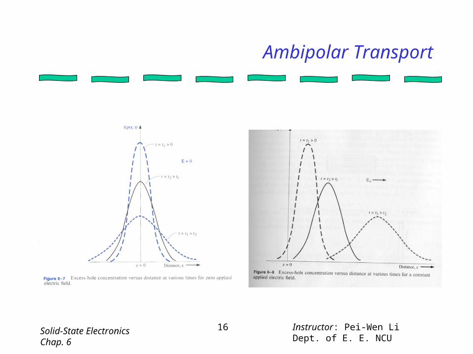
Ambipolar Transport
If a pulse of excess electrons and holes are created at a particular point due to an applied E-field, the excess e-s and h+s will tend to drift in opposite directions. However, any separation of e-s and h+s will induce an internal E-field and create a force attracting the e-s and h+s back.
The internal E-field will hold the pulses of excess e -s and h+s together, then the electrons and holes will drift or diffuse together with a single effective mobility or diffusion coefficient. This is so called “ambipolar diffusion” or “ambipolar transport”.
Fig. Show the above situation

Solid-State Electronics Chap. 6
Instructor: Pei-Wen LiDept. of E. E. NCU
15
Ambipolar Transport
Solid-State Electronics Chap. 6
Instructor: Pei-Wen LiDept. of E. E. NCU
16
Ambipolar Transport
Solid-State Electronics Chap. 6
Instructor: Pei-Wen LiDept. of E. E. NCU
17
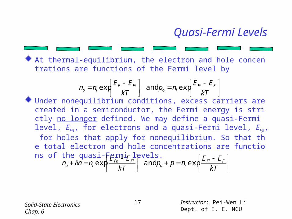
Quasi-Fermi Levels
At thermal-equilibrium, the electron and hole concentrations are functions of the Fermi level by
Under nonequilibrium conditions, excess carriers are created in a semiconductor, the Fermi energy is strictly no longer defined. We may define a quasi-Fermi level, EFn, for electrons and a quasi-Fermi level, EFp, for holes that apply for nonequilibrium. So that the total electron and hole concentrations are functions of the quasi-Fermi levels.
exp and exp
kT
EEnp
kT
EEnn FFi
ioFiF
io
exp and exp
kT
EEnpp
kT
EEnnn FFi
ioFiFn
io

Solid-State Electronics Chap. 6
Instructor: Pei-Wen LiDept. of E. E. NCU
18
Quasi-Fermi Levels
For a n-type semiconductor under thermal equilibrium, the band diagram is
Under low-level injection, excess carriers are created and the quasi-Fermi level for holes (minority), EFp, is significantly different from EF.
Solid-State Electronics Chap. 6
Instructor: Pei-Wen LiDept. of E. E. NCU
19
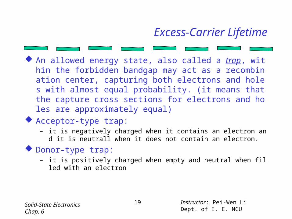
Excess-Carrier Lifetime
An allowed energy state, also called a trap, within the forbidden bandgap may act as a recombination center, capturing both electrons and holes with almost equal probability. (it means that the capture cross sections for electrons and holes are approximately equal)
Acceptor-type trap: – it is negatively charged when it contains an electron and it is neutrall when it does n
ot contain an electron.
Donor-type trap:– it is positively charged when empty and neutral when filled with an electron

Solid-State Electronics Chap. 6
Instructor: Pei-Wen LiDept. of E. E. NCU
20
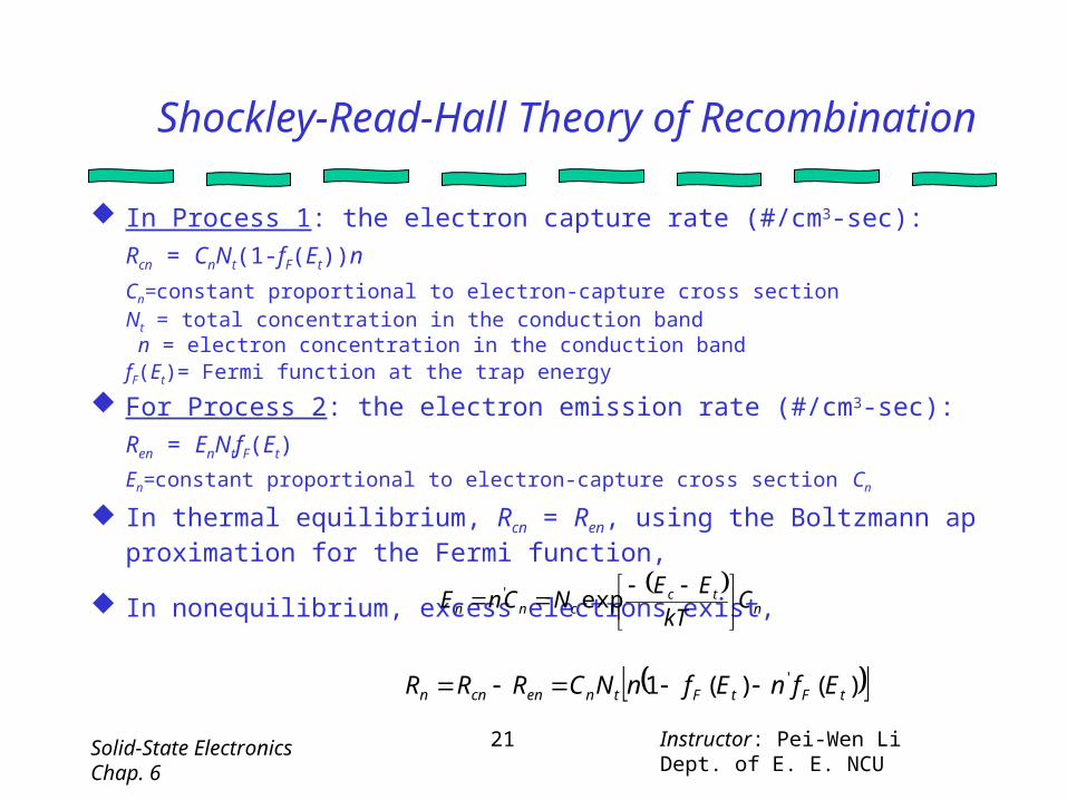
Shockley-Read-Hall Theory of Recombination
Assume that a single recombination center exists at an energy Et within the bandgap. And there are four basic processes that may occur at this single trap.
Process 1: electron from the
conduction band captured by an
initially neutral empty trap. Process 2: electron emission from a
trap into the conduction band. Process 3: capture of a hole from the
valence band by a trap containing an
electron. Process 4: emission of a hole from a
neutral trap into the valence band.
Solid-State Electronics Chap. 6
Instructor: Pei-Wen LiDept. of E. E. NCU
21
Shockley-Read-Hall Theory of Recombination
In Process 1: the electron capture rate (#/cm3-sec):
Rcn = CnNt(1-fF(Et))n
Cn=constant proportional to electron-capture cross sectionNt = total concentration in the conduction band n = electron concentration in the conduction bandfF(Et)= Fermi function at the trap energy
For Process 2: the electron emission rate (#/cm3-sec):
Ren = EnNtfF(Et)
En=constant proportional to electron-capture cross section Cn
In thermal equilibrium, Rcn = Ren, using the Boltzmann approximation for the Fermi function,
In nonequilibrium, excess electrons exist,
n
tccnn C
kT
EENCnE
exp'
)()(1 'tFtFtnencnn EfnEfnNCRRR
Solid-State Electronics Chap. 6
Instructor: Pei-Wen LiDept. of E. E. NCU
22
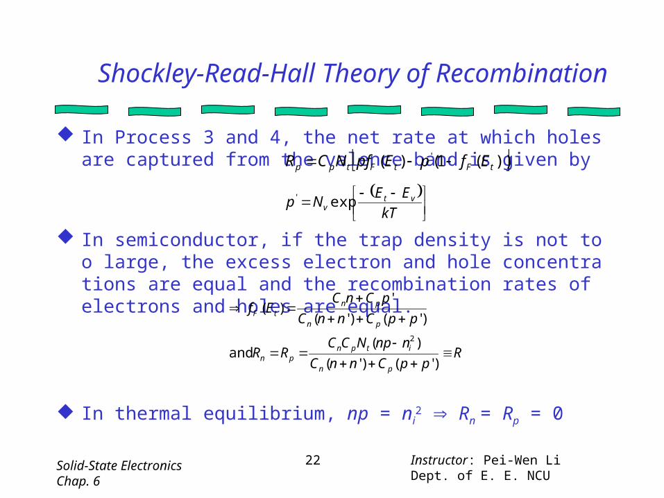
Shockley-Read-Hall Theory of Recombination
In Process 3 and 4, the net rate at which holes are captured from the valence band is given by
In semiconductor, if the trap density is not too large, the excess electron and hole concentrations are equal and the recombination rates of electrons and holes are equal.
In thermal equilibrium, np = ni2 Rn = Rp = 0
))(1()( 'tFtFtpp EfpEpfNCR
kT
EENp vt
v exp'
RppCnnC
nnpNCCRR
ppCnnC
pCnCEf
pn
itpnpn
pn
pntF
)'()'(
)( and
)'()'(
')(
2

Solid-State Electronics Chap. 6
Instructor: Pei-Wen LiDept. of E. E. NCU
23
Surface Effects
Surface states are functionally equivalent to R-G centers localized at the surface of a material. However, the surface states (or interfacial traps) are typically found to be continuously distributed in energy throughout the semiconductor bandgap.

Solid-State Electronics Chap. 6
Instructor: Pei-Wen LiDept. of E. E. NCU
24
Surface Recombination Velocity
As the excess concentration at the surface becomes smaller than that in the bulk, excess carriers from the bulk region diffuse toward the surface where they recombine, and the surface recombination velocity increases.
An infinite surface recombination velocity implies that the excess minority carrier concentration and lifetime are zero.
Solid-State Electronics Chap. 6
Instructor: Pei-Wen LiDept. of E. E. NCU
25
Homework
6.14 6.17 6.19