Embed Size (px)
Citation preview
Solar Energy Materials & Solar Cells 117 (2013) 476–482
Contents lists available at ScienceDirect
Solar Energy Materials & Solar Cells
0927-02http://d
n CorrCommeToledo,
E-m
journal homepage: www.elsevier.com/locate/solmat
Thin film solar cells based on the heterojunction of colloidal PbSquantum dots with CdS
Khagendra P. Bhandari a,n, Paul J. Roland a, Hasitha Mahabaduge a, Neale O. Haugen a,Corey R. Grice a, Sohee Jeong c, Tieneke Dykstra a, Jianbo Gao a,b,n, Randy J. Ellingson a,n
a Wright Center for Photovoltaic Innovation and Commercialization, Department of Physics and Astronomy, The University of Toledo, 2801 W. Bancroft Street,Toledo, OH 43606, USAb National Renewable Energy Laboratory (NREL), 16253 Denver West Parkway, Golden, CO 80401, USAc Nanomechanical Research Division, Korea Institute of Machinery and Materials, Daejeon 305-343, Republic of Korea
a r t i c l e i n f o
Article history:Received 25 January 2013Received in revised form9 July 2013Accepted 12 July 2013
Keywords:Quantum dotPbSCdSSolar cellThin film
48/$ - see front matter & 2013 Elsevier B.V. Ax.doi.org/10.1016/j.solmat.2013.07.018
esponding authors at: Wright Center forrcialization, Department of Physics and As2801 W. Bancroft Street, Toledo, OH 43606, Uail address: [email protected] (R.J.
a b s t r a c t
Here we report on heterojunction PbS quantum dot (QD) solar cells using RF magnetron sputtered CdS asthe n-type window layer. These solar cells generate large open circuit voltage compared to previouslyreported PbS-QD solar cells. Our investigations of this device design show an optimized CdS filmthickness of 70 nm and an optimized PbS QD diameter of ∼2.7 nm, corresponding to a bandgap energy of∼1.57 eV. Under simulated AM1.5 G illumination, we attain short circuit current as high as 12 mA-cm�2,an open circuit voltage of 0.65 V and efficiency as high as 3.3%.
& 2013 Elsevier B.V. All rights reserved.
1. Introduction
Researchers have been investigating suitable n-type hetero-partners for PbS quantum dot (QD) solar cells for several years. Todate, only ZnO and TiO2 in their various forms (nanoparticles,nanowires, and bulk thin film) have been widely used as n-typeheteropartners for PbS QDs solar cells. With these heteropartners,QD solar cells have shown promising efficiencies in the 4–7% rangeup to 7.4% [1,2]. ZnO is a wide bandgap (3.37 eV) II–VI semicon-ductor, and typically shows n-type character even in the absenceof intentional doping with low carrier concentration. The synthesisof nanocrystalline (NC) TiO2 paste for industrial productioninvolves a lengthy process which may be economically challen-ging, [3] and because of its relatively small electron affinity, TiO2
cannot be utilized for all sized PbS QDs (efficient electron transferfrom PbS QDs to TiO2 occurs only for QD diameters belowapproximately 4.3 nm) [4]. These facts, together with the desireto expand our knowledge of photovoltaic (PV) materials science,
ll rights reserved.
Photovoltaic Innovation andtronomy, The University ofSA. Tel.: +1 4195303874.Ellingson).
suggest consideration of other possible heteropartners for the PbSQDs solar cells.
In this study we have explored sputtered CdS as a hetero-partner for PbS QD solar cells for comparison with ZnO andnanostructure TiO2. CdS is a non-stoichiometric n-type semicon-ductor with a direct band gap energy of 2.42 eV [5]. We reporthere on CdS/PbS-QD heterojunction solar cells that show an opencircuit voltage as high as ∼0.65 V. To our knowledge, no previousreport has been made on photovoltaic devices based on RFmagnetron sputtered CdS as a window layer for a PbS QD thinfilm absorber layer [6].
Thin films of CdS have been studied extensively over the pastthree decades, owing in large part to the fact that CdS has been themost widely used and most successful n-type window layer forhigh efficiency thin film solar cells based on CdTe [7,8] and Cu(InGa)Se2 (CIGS) [9,10]. Various techniques such as chemical vapordeposition [11], RF magnetron sputtering [12], and chemical bathdeposition [13] have been used to make uniform and transparentCdS films to produce high efficiency solar cells. For CdS, sputteredfilms have shown both larger crystalline grain size as well assmoother surface roughness as compared with films produced bychemical bath deposition [14]; in addition, we find excellentadhesion qualities for the sputtered CdS films. Sputtering offers
K.P. Bhandari et al. / Solar Energy Materials & Solar Cells 117 (2013) 476–482 477
potential benefits in terms of deposition rate, substrate through-put, and film thickness uniformity.
2. Experimental
2.1. Materials
All chemicals, oleic acid (OA), octadecene (ODE, 495%),hexamethyldisilal-thiane ((TMS)2S), lead(II) oxide (PbO, 99.9+%),ethyl alcohol (EtOH, absolute, anhydrous), acetonitrile (99.8%anhydrous), hexane (C6H14, anhydrous, 95.0%), and 1,2-ethane-dithiol (98.0%), were purchased from Sigma-Aldrich except EtOHand OA, which were obtained from Fisher Scientific.
2.2. PbS QD synthesis
The synthesis of PbS QDs is based on the slightly modifiedversion of Hines and Scholes [15] and is carried out under an inertatmosphere using standard Schlenck line techniques. In a typicalsynthesis, for example to synthesize ∼2.9 nm diameterQDs: 2 mmol of PbO, 10 g of ODE, and 1.14 g of OA are heated to120–1221C under N2 in a 100 mL round bottom three neck flask.The mixture is continuously stirred with a magnetic stirrer. Themixture is heated until all the PbO is dissolved completelytypically within 45 min.
In the glove box, 1 mmol (TMS)2S is dissolved in 3.16 g ofnitrogen-purged ODE. The mixture is loaded in a syringe with aneedle. The heating mantle is removed and the mixture is injectedimmediately at 110 1C into a three neck flask. When the tempera-ture of the mixture reaches room temperature, purification is donein air by adding ∼5 mL of hexane and ∼30 mL of EtOH andcentrifuging at 5000 rpm for about 20 min. The supernatant isremoved and sediment is cleaned two more time with hexane/
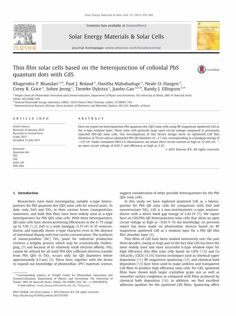
Fig. 1. (a) Schematic of the PbS QD/CdS heterojunction solar cell. (b) Cross-sectional scan(a). (c) Schematic of the energy band diagram of an ITO/CdS/PbS-QD/Au solar cell.
ethanol. QDs so obtained are dried under nitrogen and utilized forthe experimental purposes.
2.3. PbS QD solar cell fabrication
PbS-QD film (absorbing layer) fabrication was completed usingthe layer-by-layer (LbL) deposition method reported elsewhere[16,17]. Patterned indium tin oxide (ITO) coated glass substrates,obtained from Thin Film Devices, Inc., were cleaned by sonicationusing micro-90s (concentrated cleaning solution) and deionizedwater. Cleaned glass substrates were then dipped into a beakercontaining 15–20 mL of QD solution with the concentration of about8 mg/mL prepared in hexane in a 30 mL beaker followed by a secondbeaker containing 1 mM EDT solution in acetonitrile. Approximately20 to 40 dip cycles resulted in QD films of 150-200 nm thickness.Dip-coating was performed either by hand or using a dip coater fromNIMA Technology, England. The added thickness of the QD film fromeach cycle depends on the concentration of the colloidal solution andthe removal speed (typically ∼0.7 mm/s) of the substrate from thesolution. For heterojunction solar cells, CdS was used as the windowlayer (n-type semiconductor) and was deposited by RF magnetronsputtering in an Ar atmosphere. Prior to deposition of CdS, thechamber was heated to 270 1C for 30 min. The transparent andconducting ITO layer shows a sheet resistance of 32 Ω/& and formsthe top contact of the device. A 150 nm thick gold (Au) film is used asthe bottom contact and is deposited either by electron beamevaporation or thermal evaporation methods. Au was selected asthe back contact, due to its high work function, to minimize backjunction effects [1,18]. Six cells were fabricated on a single substrate,each with an active area of 0.0975 cm2.
2.4. PbS QD solution, film, and device characterization
Absorbance spectra (optical density, OD) were measured using aPerkin-Elmer, Lambda 1050, UV/VIS/NIR spectrophotometer.
ning electron microscopy (SEM) of the PbS QD/CdS junction solar cell illustrated in
K.P. Bhandari et al. / Solar Energy Materials & Solar Cells 117 (2013) 476–482478
Photoluminescence spectra (PL) were measured using FourierTransform Photoluminescence Spectroscopy (FT-PLE). Instrumentalset up of FT-PLE is very similar to the one explained by McDonaldet al. [19]. Current–voltage measurements were done with aKeithley 2440 Source-Measure Unit under illumination from anOriel 91195A-1000 solar simulator, and external quantum efficiency(EQE) measurements were acquired using a PV Measurements Inc.,Model IVQE8-C QE system. X-ray diffraction (XRD) spectra wereobtained using a Dragon/PXRD; surface roughness for the CdS andPbS-QD films were determined by AFM using a Veeco D3300 V.
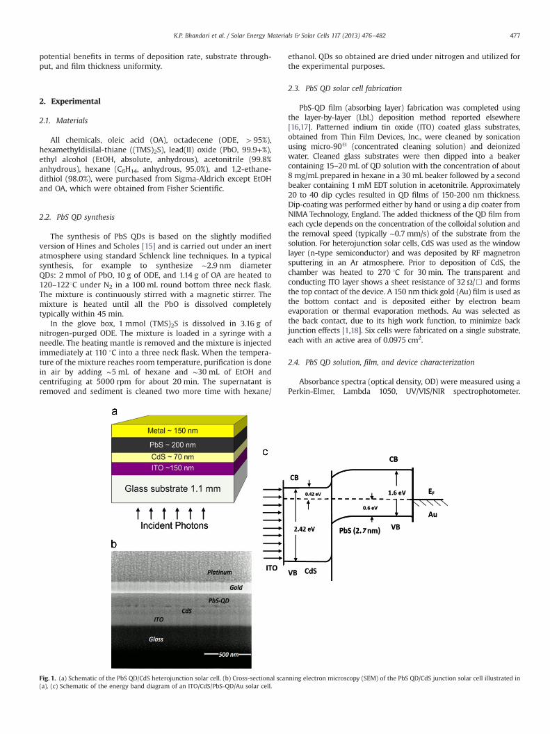
Fig. 2. Current–voltage (I–V) characteristics of a CdS/PbS-QD heterojunction solarcell recorded in the dark and under 100 mW-cm�2 simulated AM1.5 illumination.The device was assembled using ∼200 nm thick EDT treated PbS-QD film depositedfrom ∼2.7 nm diameter QDs, ∼70 nm thick CdS film and gold contact. VOC, JSC, FFand PCE of this cell were 638 mV, 12.0 mA-cm�2, 43.5% and 3.3% respectively.
3. Results and discussion
Fig. 1 shows the complete solar cell device structure, its cross-sectional view, and equilibrium band diagram. Varying the thick-nesses of both the n- and p- type layers, we found the best cellperformance using 70 nm of CdS and 150–200 nm of PbS QDs. Thecompleted device was processed for cross-sectional imaging usingfocused ion beam (FIB) milling, and imaged by scanning electronmicroscopy (SEM). A layer of platinum was deposited onto the Aulayer to avoid Ga+ ion implantation and milling of the Au surfaceduring FIB processing [20].
The X-ray diffraction pattern of CdS thin films (see SupportingInformation, Fig. S1) deposited at a sputter power of 50 W showeda most prominent diffraction peak at 2θ¼26.481, corresponding tothe (002) lattice plane of CdS. The (002) peak, as well as severalother peaks arising from (100), (002), (101), (110), (103), (200),(112), (201) and (004) lattice planes, represent the hexagonalwurtzite crystalline phase with inter-plane spacing of 5.83 Å[21,22]. Scherrer analysis of the primary diffraction peak (002)indicates that the film consists of oriented grains with an averagesize of 33 nm. The optical transmittance of the CdS film wasmeasured for the wavelength range 350–2000 nm (Fig. S2). A70 nm thick CdS film transmits at 460% for incident light ofwavelength longer than 515 nm.
In order to construct the solar cell′s band diagram, we investi-gated the electronic and interface properties of sputtered CdS andLbL PbS QD thin films. Work functions of CdS films and PbS-QDswere measured by Kelvin probe (KP) and ultraviolet photoelectronspectroscopy (UPS). Work functions of these thin films measured byKP were 4.4 eV (CdS) and 4.5 eV (PbS-QD films). Similarly, the workfunctions derived by UPS measurements were 4.5 eV (CdS) and4.9 eV (PbS-QD films). UPS was also used to calculate the valenceband maximum (VBM) for both CdS and PbS-QD films. The VBMobtained with respect to the Fermi level, which is considered as thezero binding energy in the UPS spectrum, were 2.0 eV (CdS) and0.6 eV (PbS-QD films) (Fig. S3). Liu et al. [23] found the work functionof CdS to be 4.7 eV and the VBM to be 2.2 eV using a similar method.The band offset at the interface is one of the most importantproperties for a semiconductor heterostructure device, and enablesthe design and optimization of different contacts to minimize theloss of photogenerated carriers resulting in a cell with higherconversion efficiency. X-ray photoelectron spectroscopy (XPS) andUPS were used to determine the valence band offset ΔEV andconduction band offset ΔEC at the CdS/PbS-QD heterojunction. Asdiscussed in the Supporting Information, the valence band offsetbetween CdS and PbS-QD was found to be 1.4 eV, and the deducedconduction band offset was determined to be 0.57 eV for a PbS-QD ofsize ∼2.7 nm. The carrier concentrations of the bulk CdS and PbS-QDfilms were determined using capacitance–voltage testing methodsand Mott–Schottky analysis as discussed in Supporting Information.
Under illumination, electron–hole pairs photo-generated withinthe depletion region are separated by the built-in electric field withelectrons drifting to the CdS and holes drifting to the PbS-QD layer.When the device terminals are shorted, excess electrons in the CdS
flow through the external circuit to recombine with the excessholes in the PbS QDs side—this represents the photocurrent. Thecurrent–voltage (I–V) characteristics of our best device is shown inFig. 2. To complete this device, we deposited a 70 nm thick CdS filmfollowed by a PbS-QD film (QD diameter of ∼2.7 nm, first excitonpeak at ∼792 nm, or 1.57 eV) of approximately 200 nm thickness(Fig. S4 presents absorbance and photoluminescence spectra). Thissolar cell exhibited an open circuit voltage, VOC of 638 mV, shortcircuit current, JSC of 12.0 mA-cm�2, and overall photo-conversionefficiency (PCE) of 3.3% when illuminated with 100 mW-cm�2
simulated AM1.5 G.We can compare these results with heterojunction devices
based on other partner materials such as CdS, ZnO, Bi2S3, andTiO2. Hernandez–Borja reported a study of CdS/PbS solar cellswhich were not based on quantum dot PbS. Their devices werefabricated using chemical bath deposition, and achieved an effi-ciency of ∼1.6%. The JSC value of 14 mA-cm�2 and VOC value of290 mV make sense in that the bandgap energy of bulk PbS is just∼0.4 eV and therefore their device absorbs a much larger portionof the solar spectrum [24]. In a report by Gao et al., solar cellsutilizing 1.6 eV band gap PbS QDs and NC ZnO achieved VOC, JSCand PCE values of o600 mV, o5.0 mA-cm�2 and o2.0% respec-tively [18]. Choi et al. constructed a solution processed tandemsolar cell with NC ZnO as a heteropartner within each of twojunctions formed using PbS-QD thin films of 1.0 eV and 1.6 eVband gap energies [25]. The best PbS-QD tandem solar cellattained a VOC of 0.91 V, though the JSC, FF, and PCE were all lowerthan we report here. Luther et al. constructed a 3% efficient bilayerPbS/ZnO QD heterojunction solar cell using air-stable 1.3 eV PbSQDs [26]. Comparing their results to ours at similar QD bandgapenergy, their FF is larger than we obtain, resulting in a larger PCEat similar JSC and VOC values. Recently, Brown et al. demonstratedimprovements in PCE for ZnO/PbS-QD heterojunction devicethrough the incorporation of a MoO3 interlayer between the PbSQD layer and the back contact [27]. They achieved an efficiency of3.5% from QDs having an effective bandgap of 1.3 eV and usinggold as a back contact. For larger dots their devices show slightlybetter performance than what we have achieved at the same dotsize. Employing 3.5 nm diameter PbS QDs and an approach similarto that of Brown et al., Gao et al. fabricated NC ZnO/PbS-QD solarcells showing 4.4% PCE with a JSC of 18 mA cm�2, which was at thetime the certified record QD device efficiency [1]. Rath et al. [28]employed Bi2S3 nanocrystals as an n-type semiconductor in theirp–n junction based solar cell based on p-type PbS-QD. Their best
K.P. Bhandari et al. / Solar Energy Materials & Solar Cells 117 (2013) 476–482 479
device demonstrated VOC 0.44 V, with a power conversion effi-ciency of 1.6% for 860 nm (1.4 eV bandgap energy) PbS-QDs andover 1% for 1300 nm (0.95 eV) PbS-QDs. Several other reports ofPbS QD solar cells exist with PCE results in the 3–5% range [29,30].Recently, a record QD thin film solar cell efficiency was reported byIp et al. based on a hybrid passivated PbS QD layer deposited ontoa ZnO/TiO2-coated substrate [2]. Ip et al. achieved a remarkablePCE of 7%, suggesting that further improvements lie ahead for thefield. Subsequent to submission of our manuscript, Chang et al.reported results similar to ours employing chemical-bath-deposited CdS as the window layer for their PbS-QD device andachieving comparable efficiency of 3.5% [31].
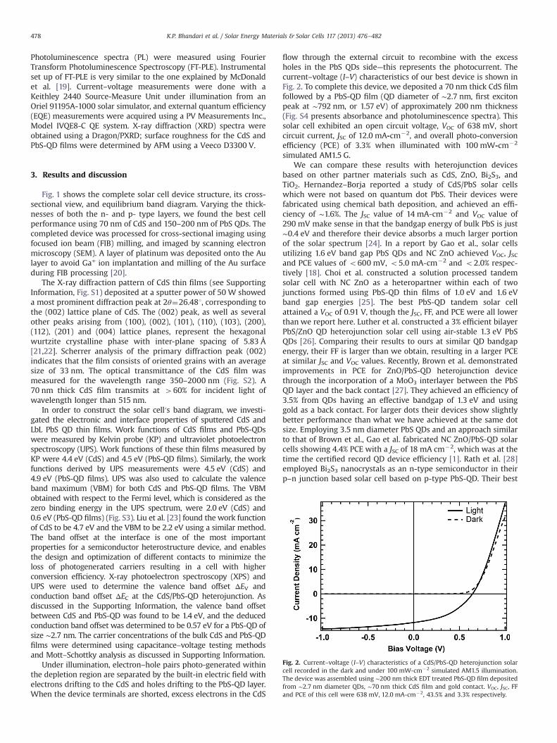
Experimental and theoretical maximum (modeled) external quan-tum efficiency (EQE) for the solar cell from Fig. 2 is shown in Fig. 3.
Fig. 3. External quantum efficiency spectrum of the PbS-QD solar cell featured inFig. 2 from both theoretically and experimentally obtained data. In the theoreticalcurve, charge collection contribution from both CdS and PbS-QD layers areconsidered and recombination losses are neglected.
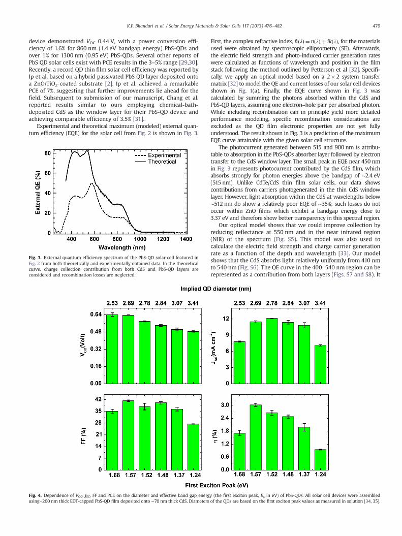
Fig. 4. Dependence of VOC, JSC, FF and PCE on the diameter and effective band gap energusing∼200 nm thick EDT-capped PbS-QD film deposited onto ∼70 nm thick CdS. Diameters
First, the complex refractive index, ~n λð Þ ¼ n λð Þ þ ik λð Þ, for the materialsused were obtained by spectroscopic ellipsometry (SE). Afterwards,the electric field strength and photo-induced carrier generation rateswere calculated as functions of wavelength and position in the filmstack following the method outlined by Petterson et al [32]. Specifi-cally, we apply an optical model based on a 2�2 system transfermatrix [32] to model the QE and current losses of our solar cell devicesshown in Fig. 1(a). Finally, the EQE curve shown in Fig. 3 wascalculated by summing the photons absorbed within the CdS andPbS-QD layers, assuming one electron–hole pair per absorbed photon.While including recombination can in principle yield more detailedperformance modeling, specific recombination considerations areexcluded as the QD film electronic properties are not yet fullyunderstood. The result shown in Fig. 3 is a prediction of the maximumEQE curve attainable with the given solar cell structure.
The photocurrent generated between 515 and 900 nm is attribu-table to absorption in the PbS-QDs absorber layer followed by electrontransfer to the CdS window layer. The small peak in EQE near 450 nmin Fig. 3 represents photocurrent contributed by the CdS film, whichabsorbs strongly for photon energies above the bandgap of ∼2.4 eV(515 nm). Unlike CdTe/CdS thin film solar cells, our data showscontributions from carriers photogenerated in the thin CdS windowlayer. However, light absorption within the CdS at wavelengths below∼512 nm do show a relatively poor EQE of ∼35%; such losses do notoccur within ZnO films which exhibit a bandgap energy close to3.37 eV and therefore show better transparency in this spectral region.
Our optical model shows that we could improve collection byreducing reflectance at 550 nm and in the near infrared region(NIR) of the spectrum (Fig. S5). This model was also used tocalculate the electric field strength and charge carrier generationrate as a function of the depth and wavelength [33]. Our modelshows that the CdS absorbs light relatively uniformly from 410 nmto 540 nm (Fig. S6). The QE curve in the 400–540 nm region can berepresented as a contribution from both layers (Figs. S7 and S8). It
y (the first exciton peak, Eg in eV) of PbS-QDs. All solar cell devices were assembledof the QDs are based on the first exciton peak values as measured in solution [34, 35].
K.P. Bhandari et al. / Solar Energy Materials & Solar Cells 117 (2013) 476–482480
is clear from Fig. 3 that a large portion of loss occurs due to poorcarrier collection and weak photon absorption in the NIR portionof the spectrum.
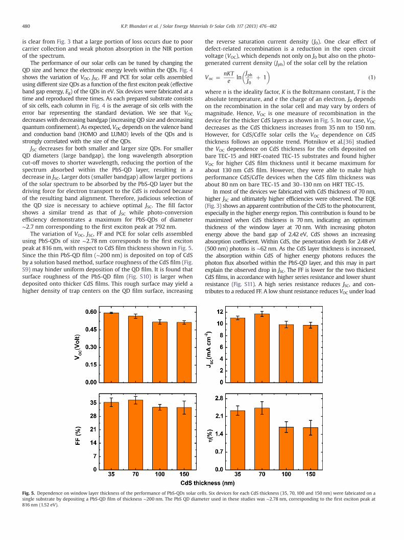
The performance of our solar cells can be tuned by changing theQD size and hence the electronic energy levels within the QDs. Fig. 4shows the variation of VOC, JSC, FF and PCE for solar cells assembledusing different size QDs as a function of the first exciton peak (effectiveband gap energy, Eg) of the QDs in eV. Six devices were fabricated at atime and reproduced three times. As each prepared substrate consistsof six cells, each column in Fig. 4 is the average of six cells with theerror bar representing the standard deviation. We see that VOCdecreases with decreasing bandgap (increasing QD size and decreasingquantum confinement). As expected, VOC depends on the valence bandand conduction band (HOMO and LUMO) levels of the QDs and isstrongly correlated with the size of the QDs.
JSC decreases for both smaller and larger size QDs. For smallerQD diameters (large bandgap), the long wavelength absorptioncut-off moves to shorter wavelength, reducing the portion of thespectrum absorbed within the PbS-QD layer, resulting in adecrease in JSC. Larger dots (smaller bandgap) allow larger portionsof the solar spectrum to be absorbed by the PbS-QD layer but thedriving force for electron transport to the CdS is reduced becauseof the resulting band alignment. Therefore, judicious selection ofthe QD size is necessary to achieve optimal JSC. The fill factorshows a similar trend as that of JSC while photo-conversionefficiency demonstrates a maximum for PbS-QDs of diameter∼2.7 nm corresponding to the first exciton peak at 792 nm.
The variation of VOC, JSC, FF and PCE for solar cells assembledusing PbS-QDs of size ∼2.78 nm corresponds to the first excitonpeak at 816 nm, with respect to CdS film thickness shown in Fig. 5.Since the thin PbS-QD film (∼200 nm) is deposited on top of CdSby a solution based method, surface roughness of the CdS film (Fig.S9) may hinder uniform deposition of the QD film. It is found thatsurface roughness of the PbS-QD film (Fig. S10) is larger whendeposited onto thicker CdS films. This rough surface may yield ahigher density of trap centers on the QD film surface, increasing
Fig. 5. Dependence on window layer thickness of the performance of PbS-QDs solar cellsingle substrate by depositing a PbS-QD film of thickness ∼200 nm. The PbS QD diame816 nm (1.52 eV).
the reverse saturation current density (J0). One clear effect ofdefect-related recombination is a reduction in the open circuitvoltage (VOC), which depends not only on J0 but also on the photo-generated current density (Jph) of the solar cell by the relation
Voc ¼ nKTe
lnJphJ0
þ 1� �
ð1Þ
where n is the ideality factor, K is the Boltzmann constant, T is theabsolute temperature, and e the charge of an electron. J0 dependson the recombination in the solar cell and may vary by orders ofmagnitude. Hence, VOC is one measure of recombination in thedevice for the thicker CdS layers as shown in Fig. 5. In our case, VOC
decreases as the CdS thickness increases from 35 nm to 150 nm.However, for CdS/CdTe solar cells the VOC dependence on CdSthickness follows an opposite trend. Plotnikov et al.[36] studiedthe VOC dependence on CdS thickness for the cells deposited onbare TEC-15 and HRT-coated TEC-15 substrates and found higherVOC for higher CdS film thickness until it became maximum forabout 130 nm CdS film. However, they were able to make highperformance CdS/CdTe devices when the CdS film thickness wasabout 80 nm on bare TEC-15 and 30–130 nm on HRT TEC-15.
In most of the devices we fabricated with CdS thickness of 70 nm,higher JSC and ultimately higher efficiencies were observed. The EQE(Fig. 3) shows an apparent contribution of the CdS to the photocurrent,especially in the higher energy region. This contribution is found to bemaximized when CdS thickness is 70 nm, indicating an optimumthickness of the window layer at 70 nm. With increasing photonenergy above the band gap of 2.42 eV, CdS shows an increasingabsorption coefficient. Within CdS, the penetration depth for 2.48 eV(500 nm) photons is ∼62 nm. As the CdS layer thickness is increased,the absorption within CdS of higher energy photons reduces thephoton flux absorbed within the PbS-QD layer, and this may in partexplain the observed drop in JSC. The FF is lower for the two thickestCdS films, in accordance with higher series resistance and lower shuntresistance (Fig. S11). A high series resistance reduces JSC, and con-tributes to a reduced FF. A low shunt resistance reduces VOC under load
s. Six devices for each CdS thickness (35, 70, 100 and 150 nm) were fabricated on ater used in these studies was ∼2.78 nm, corresponding to the first exciton peak at
K.P. Bhandari et al. / Solar Energy Materials & Solar Cells 117 (2013) 476–482 481
and also lowers the FF. Because of the bulky organic molecules in QDs,mobility of the charge carriers is low [37], RS values are higher, and RShvalues are smaller than they appear in commercial thin film solar cells.The series and shunt resistances of our best device are 21Ω cm2 and204Ω cm2 respectively. Series and shunt resistances of CdS/CdTe solarcells of device area of 0.08 cm2 obtained by Vigil et al.[38] were2.9Ω cm2 and 787Ω cm2 when S/Cd ratio was 5/1. The highestefficiency they achieved from this device is 12.3%. Similarly, from adevice area of 0.25 cm2, Pena et al. [39] obtained series and shuntresistances 8.0 Ω cm2 and 631Ω cm2 from CdS/CdTe solar cells ofefficiency 6.3% with Cu/Mo back contact.
We studied the stability of the devices by measuring their J–Vcharacteristics with respect to time following a similar procedure asTang et al. [40] For these measurements, two identical devices wereused, keeping one of the devices in ambient atmosphere and anotherin an inert N2 atmosphere. Our two month long study shows nosignificant differences between storage in ambient air and storage inan inert atmosphere as shown in Fig. S12. This indicates that theperformance of these devices does not degrade significantly in air onthe timescale of months, though longer time studies are required todetermine the extent of the air-stability of these devices.
4. Conclusions
We report the first heterojunction solar cells based on PbS-QDs andRF magnetron sputtered CdS thin films, demonstrating an achievedefficiency of 3.3%. Our devices exhibited high VOC values whencompared to Schottky junction solar cells and other PbS-QDs hetero-junction solar cells. We find that PbS-QDs with the first exciton peaknear 800 nm yielded the best devices. Similarly, CdS thin films withthicknesses of ∼70 nm are considered as an optimized window layerthickness for the CdS/PbS-QD combination. From this study, weconclude that understanding and optimizing the quality of the PbScoupled QD film, as well as the properties of the interface between theCdS and the PbS-QD film, are both essential to enhance the perfor-mance of heterojunction QD thin film solar cells in the future.
Acknowledgments
The authors would like to thank Y. Xie for his assistance tomeasure surface roughness using atomic force microscopy. K. Bhan-dari, T. Dykstra, R. Ellingson, N. Haugen, and P. Roland receivedsupport from the Air Force Research Laboratory under ContractsFA9453-08-C-0172 and FA9453-11-C-0253; CG was supported by theUniversity of Toledo′s School for Solar and Advanced RenewableEnergy; K. Bhandari and J. Gao received support from the NationalRenewable Energy Laboratory Seed Fund program; R. Ellingsonreceived support from the State of Ohio Wright Centers program;and S. Jeong was supported by the Global Frontier R&D Program bythe Center for Multiscale Energy Systems.
Appendix A. Supporting information
Supplementary data associated with this article can be found inthe online version at http://dx.doi.org/10.1016/j.solmat.2013.07.018.
References
[1] J. Gao, C.L. Perkins, J.M. Luther, M.C. Hanna, H.-Y. Chen, O.E. Semonin, A.J. Nozik, R.J. Ellingson, M.C. Beard, n-Type transition metal oxide as a holeextraction layer in PbS quantum dot solar cells, Nano Letters 11 (2011)3263–3266.
[2] A.H. Ip, S.M. Thon, S. Hoogland, O. Voznyy, D. Zhitomirsky, R. Debnath,L. Levina, L.R. Rollny, G.H. Carey, A. Fischer, K.W. Kemp, I.J. Kramer, Z. Ning,A.J. Labelle, K.W. Chou, A. Amassian, E.H. Sargent, Hybrid passivated colloidalquantum dot solids, Nat Nano 7 (2012) 577–582.
[3] S. Ito, P. Chen, P. Comte, M.K. Nazeeruddin, P. Liska, P. Péchy, M. Grätzel,Fabrication of screen-printing pastes from TiO2 powders for dye-sensitisedsolar cells, Progress in Photovoltaics: Research and Applications 15 (2007)603–612.
[4] B.-R. Hyun, Y.-W. Zhong, A.C. Bartnik, L. Sun, H.D. Abruna, F.W. Wise, J.D. Goodreau, J.R. Matthews, T.M. Leslie, N.F. Borrelli, Electron injection fromcolloidal PbS quantum dots into titanium dioxide nanoparticles, ACS Nano 2(2008) 2206–2212.
[5] D. Lincot, G. Hodes, Chemical Solution Deposition of Semiconducting and Non-Metallic Films: Proceedings of the International Symposium, ElectrochemicalSociety, 2006.
[6] Subsequent to the submission of our manuscript, the work by Chang et al. (Ref.#31) reported a study of all-solution-processed CdS/PbS solar cells in whichthe CdS thin film was prepared using chemical bath deposition. The studyachieved similar results for reported device efficiency.
[7] N. Romeo, A. Bosio, R. Tedeschi, A. Romeo, V. Canevari, A highly efficient andstable CdTe/CdS thin film solar cell, Solar Energy Materials and Solar Cells 58(1999) 209–218.
[8] K.D. Dobson, I. Visoly-Fisher, G. Hodes, D. Cahen, Stability of CdTe/CdS thin-film solar cells, Solar Energy Materials and Solar Cells 62 (2000) 295–325.
[9] K. Ramanathan, M.A. Contreras, C.L. Perkins, S. Asher, F.S. Hasoon, J. Keane,D. Young, M. Romero, W. Metzger, R. Noufi, J. Ward, A. Duda, Properties of19.2% efficiency ZnO/CdS/CuInGaSe2 thin-film solar cells, Progress in Photo-voltaics: Research and Applications 11 (2003) 225–230.
[10] R. Scheer, H.W. Schock, Chalcogenide Photovoltaics: Physics, Technologies, andThin Film Devices, John Wiley & Sons, 2011.
[11] H. Uda, H. Yonezawa, Y. Ohtsubo, M. Kosaka, H. Sonomura, Thin CdS filmsprepared by metalorganic chemical vapor deposition, Solar Energy Materialsand Solar Cells 75 (2003) 219–226.
[12] J.-H. Lee, D.-J. Lee, Effects of CdCl2 treatment on the properties of CdSfilms prepared by r.f. magnetron sputtering, Thin Solid Films 515 (2007)6055–6059.
[13] J.Y. Choi, K.-J. Kim, J.-B. Yoo, D. Kim, Properties of cadmium sulfide thin filmsdeposited by chemical bath deposition with ultrasonication, Solar Energy 64(1998) 41–47.
[14] S.L. Wang, X.J. Wang, W.Z. Wang, C.J. Liang, Z. Wang, Z. Qi, Comparative studyon thin films of cadmium sulfide prepared by chemical bath deposition andradio frequency magnetron sputtering, Guang Pu Xue Yu Guang Pu Fen Xi 32(2012) 1094–1097.
[15] M.A. Hines, G.D. Scholes, Colloidal PbS nanocrystals with size-tunable near-infrared emission: observation of post-synthesis self-narrowing of the particlesize distribution, Advanced Materials 15 (2003) 1844–1849.
[16] J.M. Luther, M. Law, M.C. Beard, Q. Song, M.O. Reese, R.J. Ellingson, A.J. Nozik,Schottky Solar Cells, Based on Colloidal Nanocrystal Films, Nano Letters 8(2008) 3488–3492.
[17] J. Tang, X. Wang, L. Brzozowski, D.A.R. Barkhouse, R. Debnath, L. Levina, E.H. Sargent, Schottky quantum dot solar cells stable in air under solarillumination, Advanced Materials 22 (2010) 1398–1402.
[18] J. Gao, J.M. Luther, O.E. Semonin, R.J. Ellingson, A.J. Nozik, M.C. Beard, Quantumdot size dependent J–V characteristics in heterojunction ZnO/PbS quantum dotsolar cells, Nano Letters 11 (2011) 1002–1008.
[19] T.J. McDonald, Near-infrared Fourier transform photoluminescence spectro-meter with tunable excitation for the study of single-walled carbon nano-tubes, Rev. Sci. Instrum. 77 (2006) 053104.
[20] B.W. Kempshall, L.A. Giannuzzi, B.I. Prenitzer, F.A. Stevie, S.X. Da, Comparativeevaluation of protective coatings and focused ion beam chemical vapordeposition processes, Journal of Vacuum Science & Technology B: Microelec-tronics and Nanometer Structures 20 (2002) 286–290.
[21] S.-G. Hur, E.-T. Kim, J.-H. Lee, G.-H. Kim, S.-G. Yoon, Characterization ofphotoconductive CdS thin films prepared on glass substrates forphotoconductive-sensor applications, Journal of Vacuum Science & Technol-ogy B: Microelectronics and Nanometer Structures 26 (2008) 1334–1337.
[22] Y.H. Sun, Y.J. Ge, W.W. Li, D.J. Huang, F. Chen, L.Y. Shang, P.X. Yang, J.H. Chu,Structural and optical analysis of CdS thin films grown by magnetronsputtering technique, Journal of Physics: Conference Series, 276 (2011) 012187.
[23] G. Liu, T. Schulmeyer, J. Brötz, A. Klein, W. Jaegermann, Interface propertiesand band alignment of Cu2S/CdS thin film solar cells, Thin Solid Films 431–432 (2003) 477–482.
[24] J. Hernández-Borja, Y.V. Vorobiev, R. Ramírez-Bon, Thin film solar cells of CdS/PbS chemically deposited by an ammonia-free process, Solar Energy Materialsand Solar Cells 95 (2011) 1882–1888.
[25] J.J. Choi, W.N. Wenger, R.S. Hoffman, Y.-F. Lim, J. Luria, J. Jasieniak, J.A. Marohn,T. Hanrath, Solution-Processed Nanocrystal Quantum Dot Tandem Solar Cells,Advanced Materials 23 (2011) 3144–3148.
[26] J.M. Luther, J. Gao, M.T. Lloyd, O.E. Semonin, M.C. Beard, A.J. Nozik, Stabilityassessment on a 3% bilayer PbS/ZnO quantum dot heterojunction solar cell,Advanced Materials 22 (2010) 3704–3707.
[27] P.R. Brown, R.R. Lunt, N. Zhao, T.P. Osedach, D.D. Wanger, L.-Y. Chang, M.G. Bawendi, V. Bulovic, Improved current extraction from ZnO/PbS quantumdot heterojunction photovoltaics using a MoO3 interfacial layer, Nano Letters11 (2011) 2955–2961.
K.P. Bhandari et al. / Solar Energy Materials & Solar Cells 117 (2013) 476–482482
[28] A.K. Rath, M. Bernechea, L. Martinez, G. Konstantatos, Solution-processedheterojunction solar cells based on p-type PbS quantum dots and n-type Bi2S3nanocrystals, Advanced Materials 23 (2011) 3712–3717.
[29] G. Zhai, A. Bezryadina, A.J. Breeze, D. Zhang, G.B. Alers, S.A. Carter, Air stabilityof TiO[sub 2]/PbS colloidal nanoparticle solar cells and its impact on powerefficiency, Applied Physics Letters 99 (2011) 063512–063513.
[30] L. Etgar, T. Moehl, S. Gabriel, S.G. Hickey, A. Eychmüller, M. Grätzel, Lightenergy conversion by mesoscopic PbS quantum dots/TiO2 heterojunctionsolar cells, ACS Nano 6 (2012) 3092–3099.
[31] L.-Y. Chang, R.R. Lunt, P.R. Brown, V. Bulović, M.G. Bawendi, Low-temperaturesolution-processed solar cells based on PbS colloidal quantum dot/CdSheterojunctions, Nano Letters 13 (2013) 994–999.
[32] L.A.A. Pettersson, L.S. Roman, O. Inganas, Modeling photocurrent actionspectra of photovoltaic devices based on organic thin films, Journal of AppliedPhysics 86 (1999) 487–496.
[33] M. Law, M.C. Beard, S. Choi, J.M. Luther, M.C. Hanna, A.J. Nozik, Determiningthe internal quantum efficiency of PbSe nanocrystal solar cells with the aid ofan optical model, Nano Letters 8 (2008) 3904–3910.
[34] L. Cademartiri, E. Montanari, G. Calestani, A. Migliori, A. Guagliardi, G.A. Ozin,Size-dependent extinction coefficients of PbS quantum dots, Journal of theAmerican Chemical Society 128 (2006) 10337–10346.
[35] I. Moreels, K. Lambert, D. Smeets, D. De Muynck, T. Nollet, J.C. Martins,F. Vanhaecke, A. Vantomme, C. Delerue, G. Allan, Z. Hens, Size-dependentoptical properties of colloidal PbS quantum dots, ACS Nano 3 (2009)3023–3030.
[36] V. Plotnikov, Fabrication of ultra thin CdS/CdTe solar cells by magnetronsputtering, University of Toledo, 2009.
[37] J. Tang, E.H. Sargent, Infrared colloidal quantum dots for photovoltaics:fundamentals and recent progress, Advanced Materials 23 (2011) 12–29.
[38] G. Vigil, O.N.A. Arias-Carbajal, P. Mendoza, R. Rez, R. Santana, G. Guez,H. Sastre, J. Ndez, J.C. Alonso, G. Moreno, E.A.G. Contreras-Puente,A. Morales-Acevedo, Improving the efficiency of CdS/CdTe solar cells byvarying the thiourea/CdCloSUB42o/SUB4 ratio in the CdS chemical bath,Semiconductor Science and Technology 20 (2005) 819–822.
[39] J.L. Peña, O. Arés, V. Rejón, A. Rios-Flores, J.M. Camacho, N. Romeo, A. Bosio, Adetailed study of the series resistance effect on CdS/CdTe solar cells with Cu/Mo back contact, Thin Solid Films 520 (2011) 680–683.
[40] J. Tang, K.W. Kemp, S. Hoogland, K.S. Jeong, H. Liu, L. Levina, M. Furukawa,X. Wang, R. Debnath, D. Cha, K.W. Chou, A. Fischer, A. Amassian, J.B. Asbury, E.H. Sargent, Colloidal-quantum-dot photovoltaics using atomic-ligand passiva-tion, Nat Mater 10 (2011) 765–771.


![Silicon-based solar cells - fotowoltaika.edu.pl. Thin-layer cells and modules ... Silicon -based solar cells – characteristics and production processes ] ] Silicon -based solar cells](https://img.pdfslide.us/doc/110x75/5b0c5ceb7f8b9a6a6b8c3d79/silicon-based-solar-cells-thin-layer-cells-and-modules-silicon-based-solar.jpg)