Embed Size (px)
Citation preview

Contents lists available at ScienceDirect
Solar Energy Materials & Solar Cells
journal homepage: www.elsevier.com/locate/solmat
Thin film iron pyrite deposited by hybrid sputtering/co-evaporation as ahole transport layer for sputtered CdS/CdTe solar cells
Khagendra P. Bhandari, Xinxuan Tan, Peymon Zereshki, Fadhil K. Alfadhili, Adam B. Phillips,Prakash Koirala, Michael J. Heben, Robert W. Collins⁎, Randy J. Ellingson⁎
Wright Center for Photovoltaics Innovation and Commercialization, Department of Physics and Astronomy, School of Solar and Advanced RenewableEnergy, The University of Toledo, 2801 West Bancroft Street, Toledo, OH 43606, USA
A R T I C L E I N F O
Keywords:Iron pyriteCdTeSolar cellsHybrid sputtering/evaporationBack contactHole transport layer
A B S T R A C T
We report the properties of hybrid deposited iron pyrite (FeS2) thin films applied as the back contact interfacelayers of CdS/CdTe solar cells. The hybrid deposition process for FeS2 optimized in this study relies on DCmagnetron sputtering of iron with simultaneous thermal evaporation of sulfur. We have fabricated solar cellsincorporating CdS/CdTe window/absorber layers sputter-deposited onto commercial transparent conductingoxide coated glass and have compared the performance of devices incorporating the new FeS2/Cu/Au backcontacts with that of standard devices incorporating Cu/Au back contacts. Considering our best devices of eachtype, the inclusion of the FeS2 thin film as a hole transport layer has improved the open circuit voltage VOC by2.1%, reaching 817 mV, and the fill-factor FF by 8.3% relative, reaching 74.7%, in comparison with devicesomitting the FeS2 layer. Under standard test conditions of 100 mA/cm2 simulated AM1.5G and 25 °C, devicesutilizing the FeS2 hole transport layer have shown a conversion efficiency η as high as 13.3% – a relativeincrease in η of ~10% over our current laboratory standard back contact. The attained FF exceeds previousresults for high efficiency sputter-deposited CdS/CdTe solar cells.
1. Introduction
Iron pyrite (FeS2) is an earth-abundant, low cost, and low-toxicitysulfur mineral and has been identified as a promising candidate thinfilm material for large-scale deployment of solar-to-electricity genera-tion [1,2]. FeS2 exhibits an indirect bandgap of ∼0.95 eV, but alsodisplays desirable high optical absorption starting in the near infra-rednear ∼1 eV and extending into the visible spectral range, thus enablingrelatively thin absorber layers that serve to minimize materials cost [2–5]. Although iron pyrite has been extensively researched for photo-voltaic (PV) applications since the mid-1980s [2], the record conver-sion efficiency of just 2.8% shows that FeS2 has not been implementedsuccessfully as an absorber for high efficiency PV cells [2,6–8]. Werecently discovered, however, that certain properties shared by mostpolycrystalline and nanocrystalline (NC) FeS2 pyrite thin films, includ-ing a high free hole (p+) density and a relatively deep work function(≳5.0 eV), support its application as a low-resistance hole transportlayer (HTL) at the back contact of CdS/CdTe solar cells. Previously, wereported the use of a solution processed FeS2 thin film, based oncolloidal FeS2 NCs, at the back contact to CdTe [9]. The deposited NCfilm, which was chemically modified using hydrazine to improve
conductivity, yielded a relative improvement in solar conversionefficiency of > 5% when compared with test cells using our laboratorystandard Cu/Au back contact. We briefly review here additionalproperties of the NC-based FeS2 back contact layers before introducingthe hybrid sputter/co-evaporation method utilized for deposition of theback contact layer of CdS/CdTe solar cells as described in this manu-script.
The cubic FeS2 NCs utilized in the solution-process back contacthave an average edge length of ∼100 nm, and thin films prepared withthat material are porous [10,11], with a void fraction of ~0.5 asdetermined by spectroscopic ellipsometry (SE) [11]. As a result, anFeS2 NC film of at least 1 µm thickness is required to minimize theadverse effect of film porosity when applying FeS2 NCs as a backcontact layer and to enhance the performance of the solar cells [9,12].When preparing the FeS2 NC film, a hydrazine treatment enhances filmconductivity by removing surfactant molecules present during and afterNC synthesis. Despite potential advantages in terms of simplicity andcost, solution-based fabrication of thin films may not prove to beeconomically viable for large scale production. In addition, the use ofhydrazine is clearly undesirable based on volatility and toxicity con-cerns.
http://dx.doi.org/10.1016/j.solmat.2017.01.044Received 13 August 2016; Received in revised form 22 December 2016; Accepted 29 January 2017
⁎ Corresponding authors.E-mail addresses: [email protected] (R.W. Collins), [email protected] (R.J. Ellingson).
Solar Energy Materials & Solar Cells 163 (2017) 277–284
0927-0248/ © 2017 Elsevier B.V. All rights reserved.
MARK

Motivated by these issues, we report here for the first time thedevelopment and demonstration of a hybrid vacuum depositionmethod for preparing polycrystalline iron pyrite thin films on CdTeabsorber layer surfaces. While many methods have been published forproducing iron pyrite thin films, ours represents one that allows for lowsubstrate temperatures while yielding high pyrite phase purity. Thismethod relies on sputtering iron and concurrently evaporating sulfur toform an iron pyrite back contact on a CdCl2-activated CdS/CdTe filmstack held at elevated temperatures, but at least ~50 °C below theactivation temperature. Our investigations have revealed favorableinitial results, with CdS/CdTe/FeS2 devices showing improvements inthe open circuit voltage (VOC), fill-factor (FF), and power conversionefficiency (η) under AM1.5G simulated solar illumination. The effi-ciency of our highest performance device (η=13.3%) prepared on acommercial transparent conducting oxide coated glass using the ironpyrite HTL compares well with the previously reported record effi-ciency of 14.0% for an all-sputtered CdS/CdTe thin film solar cellprepared on optimized ZnO:Al [13] In fact, the FF for the highestefficiency cell using the iron pyrite HTL reported here exceeds thatreported for the best cells in Ref. [13].
2. Experimental details
The cadmium sulfide (CdS) window and CdTe absorber layers of allsolar cells were deposited by RF magnetron sputtering onto TEC™ 15soda lime glass substrates coated with a 100 nm thick high resistivitytransparent layer (HRT; Pilkington N. A.) [14]. The thicknesses of CdSand CdTe films were ∼80 nm and ∼2 µm, respectively. For character-ization purposes, polycrystalline iron pyrite (FeS2) films were preparedon uncoated soda lime glass and on silicon wafer substrates. Inaddition to these latter substrates, (TEC™ 15)/HRT/CdS/CdTe, withCdCl2 activation, served as the underlying structure for FeS2 filmincorporation into PV devices. These devices were completed bydeposition of a metal bilayer of Cu/Au to cap the FeS2 interface layerof the back contact. The bilayer consists of ∼3 nm Cu and ∼40 nm Authermally evaporated sequentially onto either the CdCl2 activated CdTelayer, in the case of the control cells, or onto the hybrid deposited FeS2layer for the novel cells. Subsequently, Cu is diffused by annealing at150 °C in dry air for 40 min. For the standard back contact depositionused in the fabrication of control cells in this study, all processes wereidentical with the exception of the FeS2 deposition which was notperformed for the control cells.
The FeS2 films were prepared in a hybrid process whereby the Fewas sputtered using a DC magnetron source and the elemental sulfur(S) was evaporated simultaneously using a thermal source. The FeS2films were deposited over a range of calibrated substrate temperaturesfrom ∼165 °C to ∼340 °C, 4 m Torr Ar pressure, and 70 W DCsputtering power. Another important parameter found to control theformation of high quality iron pyrite for use in devices is the sulfurevaporation rate (SER). Several SERs were attempted and high crystal-line quality pyrite was obtained when the SER was in the range from∼0.2 nm/s to ∼0.4 nm/s, associated with an iron pyrite deposition raterange from ~0.1 to 0.2 nm/s at the Fe sputtering power given above.Depending on the purpose of the FeS2 film, the deposition time wasvaried from 5 min to 1 h, yielding film thicknesses at these extremes ofdeposition duration ranging from ∼30 nm to ∼750 nm, respectively.When FeS2 films were prepared as an HTL for CdS/CdTe solar cells,film thicknesses of < 100 nm were preferred. The thicker films wereused for materials characterization. Although a complete study of thedependence of device performance on FeS2 film thickness has not beenperformed, a reduced thickness is beneficial because it reduces (i) thedeposition time, (ii) the thickness of Cu as a component of the Cu/Aumetal contact, and (iii) the time and temperature required for Cudiffusion during processing.
For devices incorporating the FeS2 HTL and for those serving ascontrols, the cell areas of 0.085 cm2 were defined by laser scribing.
Quantum efficiency (QE) measurements confirmed the measured JSCvalues. Current density vs. voltage measurements were performed inthe dark, and under 1 Sun AM1.5G illumination. The crystal structureand purity of FeS2 films were determined by X-ray diffraction (XRD,Rigaku Ultima III X-ray Diffractometer) and Raman spectroscopy(Jobin Yvon Horiba Confocal Raman Spectrometer) measurements,surface morphology was determined using scanning electron micro-scopy (SEM, Hitachi S-4800), and material stoichiometry was deter-mined by energy dispersive X-ray (EDX) spectroscopy in the sameSEM. XRD patterns were analyzed to obtain information on the crystalstructure along with the lattice constants at different Miller indices forthe samples prepared at different substrate temperatures and also atdifferent SER values. For XRD, SEM, and EDX measurements, FeS2films were deposited primarily onto soda lime glass substrates, butthese measurements were also conducted when the films were depos-ited onto c-Si substrates.
Absorbance spectra of the films were measured using a spectro-photometer (Perkin Elmer Lambda 1050). Spectroscopic ellipsometry(SE) of the films was performed as well, using a multichannelellipsometer (J. A. Woollam Co., M2000DI). For these optical char-acterization techniques, FeS2 thin films were fabricated on soda limeglass and c-Si substrates. For determination of the dielectric functionsof the films by SE, the FeS2 thin films were deposited on c-Si substratesand were cooled to room temperature before in situ measurement. Insitu measurement avoided surface oxidation, and the ellipsometryspectra were corrected for surface roughness layers whose character-istics were determined from real time analysis of the film growthprocesses. The c-Si substrates were also used to calibrate the substratetemperature in the deposition chamber by applying in situ SE.
3. Results and discussion
The current density-voltage (J-V) curves are shown in Fig. 1 for thehighest efficiency sputtered CdTe devices using novel FeS2/Cu/Au andstandard Cu/Au back contacts. The solid and dashed lines depict theresults of light and dark measurements, respectively. The associatedperformance parameters shown in Table 1 represent average valuesfrom 20 cells for both the FeS2/Cu/Au and the Cu/Au back contacts.The metal Au with its relatively high work function, ϕ≈5.0 eV, is chosenfor the standard back contact to minimize the effect of an opposingdiode created by a Schottky barrier at the CdTe/metal interface [15].From the J-V curves shown in Fig. 1 and the parameter values inTable 1, it can be seen that adding a thin film of FeS2 as an interfacelayer between CdTe and the metal Au improves the device perfor-mance. Whereas JSC is similar for both novel and standard back contact
Fig. 1. Current voltage characteristics for the best-performing sputtered CdTe solar cellsusing standard and novel back contacts as indicated; approximate thicknesses for thecomponents of each of the two back contacts are shown in the graph. JSC was verified byexternal quantum efficiency measurements.
K.P. Bhandari et al. Solar Energy Materials & Solar Cells 163 (2017) 277–284
278
types, increases in both VOC and FF (in accord with improved seriesand shunt resistance values) result in increased device efficiency whenapplying the FeS2/Cu/Au back contact to the sputtered CdTe solar cell.The increase in VOC is more than 2% and the increase in FF is morethan 8% with the FeS2/Cu/Au back contact as shown in Fig. 1.
The improvement in device performance observed here for <100 nm thick FeS2 HTLs deposited by the hybrid process replicatesthat observed when using ~1 µm thick nanocrystalline FeS2 (FeS2-NC)interface layers [9]. In addition to the significantly different method ofFeS2 preparation (hybrid sputtering/co-evaporation used here versusthe solution process used previously), the results reported here derivefrom a different method of Cu incorporation and diffusion. For thehybrid sputtered/co-evaporated FeS2 thin film, the FeS2 is firstdeposited onto the activated CdTe surface, and the device is subse-quently completed by evaporating Cu/Au and annealing the device todiffuse the Cu. In contrast, in the previous study of the solution-processed FeS2 back contact layer, Cu is introduced and diffused intothe activated CdTe prior to deposition of the FeS2-NC layer andevaporation of the Au layer. In this latter case, no thermal processingis used during or subsequent to the FeS2-NC or Au depositions.
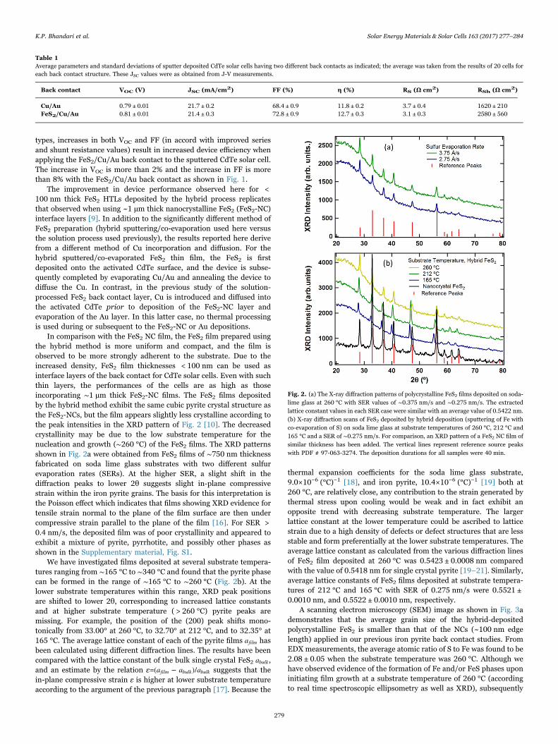
In comparison with the FeS2 NC film, the FeS2 film prepared usingthe hybrid method is more uniform and compact, and the film isobserved to be more strongly adherent to the substrate. Due to theincreased density, FeS2 film thicknesses < 100 nm can be used asinterface layers of the back contact for CdTe solar cells. Even with suchthin layers, the performances of the cells are as high as thoseincorporating ∼1 µm thick FeS2-NC films. The FeS2 films depositedby the hybrid method exhibit the same cubic pyrite crystal structure asthe FeS2-NCs, but the film appears slightly less crystalline according tothe peak intensities in the XRD pattern of Fig. 2 [10]. The decreasedcrystallinity may be due to the low substrate temperature for thenucleation and growth (∼260 °C) of the FeS2 films. The XRD patternsshown in Fig. 2a were obtained from FeS2 films of ∼750 nm thicknessfabricated on soda lime glass substrates with two different sulfurevaporation rates (SERs). At the higher SER, a slight shift in thediffraction peaks to lower 2θ suggests slight in-plane compressivestrain within the iron pyrite grains. The basis for this interpretation isthe Poisson effect which indicates that films showing XRD evidence fortensile strain normal to the plane of the film surface are then undercompressive strain parallel to the plane of the film [16]. For SER >0.4 nm/s, the deposited film was of poor crystallinity and appeared toexhibit a mixture of pyrite, pyrrhotite, and possibly other phases asshown in the Supplementary material, Fig. S1.
We have investigated films deposited at several substrate tempera-tures ranging from ∼165 °C to ∼340 °C and found that the pyrite phasecan be formed in the range of ∼165 °C to ∼260 °C (Fig. 2b). At thelower substrate temperatures within this range, XRD peak positionsare shifted to lower 2θ, corresponding to increased lattice constantsand at higher substrate temperature ( > 260 °C) pyrite peaks aremissing. For example, the position of the (200) peak shifts mono-tonically from 33.00° at 260 °C, to 32.70° at 212 °C, and to 32.35° at165 °C. The average lattice constant of each of the pyrite films afilm hasbeen calculated using different diffraction lines. The results have beencompared with the lattice constant of the bulk single crystal FeS2 abulk,and an estimate by the relation ε= a a a( − )/film bulk bulk suggests that thein-plane compressive strain ε is higher at lower substrate temperatureaccording to the argument of the previous paragraph [17]. Because the
thermal expansion coefficients for the soda lime glass substrate,9.0×10−6 (°C)−1 [18], and iron pyrite, 10.4×10⁻⁶ (°C)−1 [19] both at260 °C, are relatively close, any contribution to the strain generated bythermal stress upon cooling would be weak and in fact exhibit anopposite trend with decreasing substrate temperature. The largerlattice constant at the lower temperature could be ascribed to latticestrain due to a high density of defects or defect structures that are lessstable and form preferentially at the lower substrate temperatures. Theaverage lattice constant as calculated from the various diffraction linesof FeS2 film deposited at 260 °C was 0.5423 ± 0.0008 nm comparedwith the value of 0.5418 nm for single crystal pyrite [19–21]. Similarly,average lattice constants of FeS2 films deposited at substrate tempera-tures of 212 °C and 165 °C with SER of 0.275 nm/s were 0.5521 ±0.0010 nm, and 0.5522 ± 0.0010 nm, respectively.
A scanning electron microscopy (SEM) image as shown in Fig. 3ademonstrates that the average grain size of the hybrid-depositedpolycrystalline FeS2 is smaller than that of the NCs (~100 nm edgelength) applied in our previous iron pyrite back contact studies. FromEDX measurements, the average atomic ratio of S to Fe was found to be2.08 ± 0.05 when the substrate temperature was 260 °C. Although wehave observed evidence of the formation of Fe and/or FeS phases uponinitiating film growth at a substrate temperature of 260 °C (accordingto real time spectroscopic ellipsometry as well as XRD), subsequently
Table 1Average parameters and standard deviations of sputter deposited CdTe solar cells having two different back contacts as indicated; the average was taken from the results of 20 cells foreach back contact structure. These JSC values were as obtained from J-V measurements.
Back contact VOC (V) JSC (mA/cm2) FF (%) η (%) RS (Ω cm2) RSh (Ω cm2)
Cu/Au 0.79 ± 0.01 21.7 ± 0.2 68.4 ± 0.9 11.8 ± 0.2 3.7 ± 0.4 1620 ± 210FeS2/Cu/Au 0.81 ± 0.01 21.4 ± 0.3 72.8 ± 0.9 12.7 ± 0.3 3.1 ± 0.3 2580 ± 560
Fig. 2. (a) The X-ray diffraction patterns of polycrystalline FeS2 films deposited on soda-lime glass at 260 °C with SER values of ∼0.375 nm/s and ∼0.275 nm/s. The extractedlattice constant values in each SER case were similar with an average value of 0.5422 nm.(b) X-ray diffraction scans of FeS2 deposited by hybrid deposition (sputtering of Fe withco-evaporation of S) on soda lime glass at substrate temperatures of 260 °C, 212 °C and165 °C and a SER of ∼0.275 nm/s. For comparison, an XRD pattern of a FeS2 NC film ofsimilar thickness has been added. The vertical lines represent reference source peakswith PDF # 97-063-3274. The deposition durations for all samples were 40 min.
K.P. Bhandari et al. Solar Energy Materials & Solar Cells 163 (2017) 277–284
279

we observe the formation of iron pyrite atop the initial layer. Atsubstrate temperatures lower than 260 °C, the S/Fe ratio is observed toincrease above 2.00 (Fig. 3b). In addition, for these lower substratetemperatures, we observe XRD patterns associated with iron pyrite, butshifted in accordance with an increasing level of in-plane compressivestrain. Thus, these results are inconsistent with the concept of atransition from cubic pyrite to the hexagonal troilite (lattice spacingslarger than those of iron pyrite) as the substrate temperature isreduced. Evidence for such a cubic to hexagonal transition occurs inthis study for the depositions at the high temperatures for which the S/Fe ratio has decreased to ~1 (Fig. 3b). Thus, the FeS phase appearing atsubstrate temperatures of 312 °C and 340 °C is consistent with theconversion of any pyrite phase to troilite.
The electrical characterization of the hybrid-deposited FeS2 wasconducted using Hall effect measurements to obtain information oncarrier type, free carrier density, and mobility. We found that thepolycrystalline FeS2 films are p-type with a net free hole density of~1020 cm−3 and a hole mobility of ∼8 cm2/Vs. The hole mobility valuefor these FeS2 films is higher than that for FeS2-NC films. We expectthat the mobility of holes within each NC, however, is likely to exceedthe mobility of holes in the hybrid deposited thin film. This expectationis based on the higher apparent crystallinity of FeS2 NC films, asindicated by XRDmeasurement. The observed lower mobility of the NCcomposite film compared to the hybrid film may then be due to theporosity of the NC film and the presence of organic surfactant
molecules. The increased mobility observed in the hybrid-depositedfilms is expected to yield a reduced contact resistance which wouldcorrelate with improved transport of holes from the CdTe to the Aulayer, which may in turn improve the open circuit voltage.
Optical measurements have also been performed on the hybrid-deposited thin films, including transmittance and reflectance spectro-scopy for optical density and absorption coefficient determination overthe range from 300 to 2000 nm (Fig. 3c) and spectroscopic ellipso-metry for dielectric function determination over the range from 0.75 to5 eV (Fig. 3d). From the absorption coefficient of the optimum FeS2film deposited at 260 °C, the results may suggest significant sub-bandgap optical absorption extending to photon energies below theexpected bandgap energy of 0.95 eV. Another interpretation, supportedby real time SE, however, is non-uniformity with depth in the filmcharacterized by a sulphur-poor region at the interface to the substrate.The dielectric functions (Fig. 3d) show features at 1.8 eV and 3.8 eVcorresponding to those of the iron pyrite natural crystal; however, thedielectric function amplitudes for the hybrid-deposited film are weakerthan that of the natural crystal, but much stronger than that of the thickNC layer as reported by Subedi et al. [11]. Applying the Bruggemaneffective medium approximation over the entire spectral range, the thinfilm exhibits a void content of 21 vol% measured relative to the naturalcrystal which, although considerable, is much lower than that of the NClayer at 62 vol% as determined by the same method.
Iron pyrite thin films of ∼200 nm to ∼500 nm thickness produced
Fig. 3. (a) SEM image of an iron pyrite film deposited by hybrid sputtering/co-evaporation at 260 °C with a SER of 0.25 nm/s; (b) EDX data for films deposited by hybrid sputtering/co-evaporation at a SER of 0.25 nm/s; (c) optical density and absorption coefficient of an iron pyrite thin film fabricated by the hybrid sputtering/co-evaporation method on a soda limeglass substrate; the thickness of the film is ∼110 nm obtained in a 12 min deposition. The substrate temperature was 260 °C and the SER was ~0.25 nm/s; (d) dielectric functions ofthree different iron pyrite materials measured at room temperature, including results for a hybrid sputtered/evaporated film of this study obtained in situ (solid lines) in comparisonwith results for a natural iron pyrite crystal [11] and an ~1.85 µm thick layer of iron pyrite nanocrystals [11], the latter two obtained ex situ. The hybrid-deposited thin film wasfabricated on a c-Si substrate at a temperature of 260 °C and a SER of ∼0.3 nm/s. This film exhibited a total bulk layer thickness of 54 nm and a surface roughness layer thickness of5 nm. The ellipsometry spectra for the film were corrected for the effects of the surface roughness and underlying film structure in order to extract (by inversion) the dielectric functionwhich was parameterized using an oscillator model.
K.P. Bhandari et al. Solar Energy Materials & Solar Cells 163 (2017) 277–284
280
by hybrid deposition have been found to produce no significantphotocurrent when used as absorber layers in Schottky and hetero-junction solar cells. As shown in Fig. 1, however, improvement indevice performance can be observed clearly when using hybrid-deposited FeS2 as an interface layer at the back contact of the CdTesolar cell. We ascribe the performance improvements to a reduced backcontact barrier, and to the potential for electron-reflecting behavior ator near the CdTe/FeS2 interface. The back contact barrier heights (Φb)as calculated from the temperature dependent J-V measurement are0.353 ± 0.011 eV for standard Cu/Au and 0.217 ± 0.008 eV for theFeS2/Cu/Au back contact. Thus, a ~130 meV reduction in barrierheight is observed upon addition of the FeS2 layer, as shown in theSupplementary material. Even with the reduced barrier to hole transferwhen FeS2 is incorporated, Cu continues to play an important role inmaximizing the cell performance. When omitting the FeS2 layer, 3 nmof Cu followed by 40 nm of Au are evaporated directly onto theactivated CdTe surface, and the device is annealed to diffuse Cu intoCdTe to increase the free hole concentration. The increased free holedensity at the back of the CdTe layer increases its conductivity, narrowsthe residual back barrier width, and enhances the tunneling probabilityfor holes through the back barrier into the Au contact layer [22,23].Although an increased amount of Cu may improve the initial backcontact performance, excess Cu is understood to degrade efficiencyfollowing thermal cycling over long durations in the field [24]. We findthat a ∼3 nm thick evaporated Cu layer is optimum for a ∼2 µm thicksputtered CdTe absorber. If we assume that 3 nm Cu diffuses uniformlythroughout a 2 µm CdTe layer, the number concentration of Cu atomsis ∼1.3×1020 cm−3. The Cu however is not uniformly distributed [25],and due to compensation only a small fraction of the Cu atoms(∼0.001) are ionized to produce free holes [26]. Even with this highaverage concentration of Cu, however, the back barrier effect is notcompletely eliminated as shown by temperature dependent J-V curves[27,28].
To reduce the back barrier more effectively, an intermediatesemiconductor layer can be deposited before the back contact layers.With suitable band edge energetics, the intermediate semiconductorlayer decreases the contact resistance, resulting in improved perfor-mance of the CdTe solar cell by promoting hole transport from theCdTe into the back contact metal. Fahrenbruch [29] in 1987, and Riouxet al. [30] in 1993, proposed ZnTe as an ohmic back contact for CdTesolar cells, and indeed ZnTe is used at present in some commercialCdTe modules [31]. This semiconductor exhibits a larger bandgapenergy than CdTe, a negligible valence band offset relative to CdTe, anda carrier concentration on the order of 1018 cm−3 when doped with Sb[30,32]. We find that the FeS2 film plays an apparently analogous roleto ZnTe, enhancing both VOC and FF. Although not yet experimentallyinvestigated in detail, we propose that the hybrid-deposited polycrys-talline FeS2 film forms an ohmic contact to Au and that the CdTe/FeS2junction shows a valence band offset favoring efficient transfer of holes.Further studies are planned to investigate and optimize band edgeoffsets for this system.
The external quantum efficiency (EQE) spectra shown in Fig. 4aindicate that the incorporation of the FeS2 film as a back contact layerin the CdTe solar cell has slightly improved current collection in thelong wavelength region of λ > 700 nm. Electron-hole pairs generatedaway from the CdS/CdTe junction, predominantly by these longwavelength photons, benefit from the lower barrier potential presentwithin the CdTe/FeS2/Au contact. Since the Cu is deposited anddiffused after FeS2 layer deposition, the conductivities of both theFeS2 and CdTe films may have increased as a result. The 5–10 nm blue-shift in the long wavelength EQE cut-off observed for CdTe devicesusing the FeS2-NC processed back contact [9] has not been observed inthis study.
Although the influence of diffusing Cu on the properties of the ironpyrite layer has yet to be studied, we tested the influence of threedifferent thicknesses of evaporated Cu on the device performance. In
these experiments, we evaporated 3 nm, 4 nm, and 5 nm thick Culayers onto the hybrid-deposited FeS2, and devices were then com-pleted in the standard manner including the steps of Au evaporationand annealing. Current density-voltage characteristics are shown inFig. 4b for CdS/CdTe devices incorporating the three different thick-nesses of Cu in the FeS2/Cu/Au back contact. In this study we did notobserve significant variation in the performance of the devices. Basedon these results, we conclude that ∼3 nm Cu is sufficient to provide thehighest performance when the FeS2 thickness is ∼50 nm. Applicationof a thicker FeS2 layer degrades the solar cell performance unless anincreased thickness of Cu is deposited. The presence of elemental Cuand iron pyrite may potentially yield chalcopyrite formation through amechanism that could be considered Cu “gettering” whereby the pyriteserves as a sink for diffusing Cu. Based on the results of Fig. 4b, therelative insensitivity of device performance with Cu deposition (3–5 nm) suggests that any gettering mechanism is not playing a key rolein determining performance.
Although solar cell parameters such as VOC, JSC, FF, PCE, RS andRSh are well accepted indicators of solar cell's performance, additionalinformation can be obtained by analyzing the J-V curves with the helpof a general single exponential diode equation given in Eq. (1).
⎡⎣⎢
⎤⎦⎥J J e
nk TV R J G V J= exp ( − ) + − ,
BS Sh L0
(1)
where e is the electronic charge, n is the diode ideality factor, kB isBoltzmann's constant, T is temperature, J0 is the reverse saturationcurrent, RS is the series resistance, GSh is the shunt conductance andJL is the current density at AM1.5G, one sun illumination.
Using the experimental J-V curves and diode equation, severalimportant parameters including ideality factor, diode saturation cur-rent density, series resistance, and shunt conductance can be calculatedand compared. These diode parameters help to understand bothqualitative and quantitative information obtained from the J-V curves.Here we experimentally determine these diode parameters to under-stand the behavior of solar cells by preparing a succession of plotsshown in Figs. 5 and 6 for both light and dark measurements. Figs. 5aand 6a show J-V data in the standard form using linear scales for bothlight and dark measurements. In both cases, current density in forwardbias increases more rapidly for devices incorporating FeS2. Thisindicates that the thin film of FeS2 incorporated into the device helpsto lower the series resistance and increase shunt resistance, leading toimproved FF and VOC of the devices.
For both back contact types and in both light and dark measure-ments, dJ/dV was found to be constant and negligible when plotted asa function of V in reverse bias and in low forward bias regions, asshown in Figs. 5b and 6b. This indicates that shunt resistance of cellswith both back contacts are sufficiently high such that the conversionefficiency is not limited measurably. Since dJ/dV of the J-V curve isvery small, noise is evident especially for the Cu/Au back contact underillumination (Fig. 5b). In the low forward bias region, the first term inthe derivative of Eq. (1) is negligible and dJ/dV then is equal to GSh.When the forward bias increases, however, the first term of thederivative increases exponentially.
Ideality factors were calculated by plotting the derivative dV/dJfrom the exponential diode equation as a function of the reciprocal of J+JSC when the devices were illuminated and as a function of thereciprocal of J when the devices were not illuminated, as shown inFigs. 5c and 6c. In these cases, the series resistance RS and idealityfactors n were obtained from the y-intercept and the slope (nkBT/e) ofthe diode equation, respectively. The ideality factors calculated usingthis method for Cu/Au and FeS2/Cu/Au back contacts were 2.6 and 2.2under illumination and 2.1 and 1.8 in the dark, respectively. Slightlyhigher values of n under illumination are observed because the data arenot precisely linear for the Cu/Au back contact. The series resistancesof the devices with Cu/Au and FeS2/Cu/Au back contacts were
K.P. Bhandari et al. Solar Energy Materials & Solar Cells 163 (2017) 277–284
281

1.3 Ω cm2 and 1.2 Ω cm2, respectively, under illumination and12.3 Ω cm2 and 7.0 Ω cm2 in the dark, respectively. These n and RSvalues for the device with Cu/Au back contacts are similar to valuesreported elsewhere [33].
Semi-logarithmic graphs of ln[J+JSC] versus V−RSJ were plottedusing the values of RS obtained above for light measurement as shownin Fig. 5d. Since JSC is zero in the dark, ln[J] was plotted versus V-RSJfor data collected in the dark. A linear region with at least 1–2 orders ofmagnitude increase in current density on a log scale is fit using Eq. (1)for the diodes in the light and dark to calculate J0 and n for cells withCu/Au and FeS2/Cu/Au back contacts. The values of n were 2.7 and 2.3under illumination and 2.3 and 2.0 in the dark for Cu/Au and FeS2/Cu/Au back contacts, respectively. The higher values of n are due to thelarge deviation in the current for the Cu/Au back contact under light
and dark conditions. These values are higher than those extracted usingthe derivatives [comparing Figs. 5c and 6c]. Similarly, the reversesaturation current densities of CdTe solar cells incorporating Cu/Auand FeS2/Cu/Au back contacts were found to be 2.4×10⁻⁴ mA/cm2 and2.7×10−5 mA/cm2 under illumination and 4.3×10⁻⁵ mA/cm2 and2.5×10−6 mA/cm2 in the dark, respectively. The n and J0 valuescalculated here for devices with Cu/Au and FeS2/Cu/Au back contactsare higher than those determined by Hegedus et al. (n=1.7 andJ0=8×10
−8 mA/cm2) for dark measurement; however, their valueswere not presented for light measurement [34]. The solar cell fabrica-tion process described by the authors of reference [34] resembles thatused here, with the device structure of glass/SnO2/CdS/CdTe/metaland an absorber layer thickness varying over the range of 2–4 µm.
Overall, by observing the J-V parameters from the light/dark
Fig. 4. (a) Typical external quantum efficiency (EQE) of sputter-deposited CdTe devices without and with the FeS2 hole transport layer. The small differences at short wavelength maybe attributed to thinner CdS for the cell with standard Cu/Au back contacts. The differences at long wavelengths may be attributed to enhanced electron and hole collection from deeplyabsorbed photons; (b) J-V behavior for CdTe solar cells with FeS2/Cu/Au back contacts. The thicknesses of the FeS2 and the Au layers were held constant whereas the Cu layer thicknesswas varied as indicated.
Fig. 5. Analysis of light current density versus voltage characteristics: (a) light J-V curves on a linear scale, (b) shunt characterization, (c) dV/dJ versus 1/(J+JSC) for calculation of nand RS, and (d) semi-log scale for calculation of J0 and n. All panels provide comparisons of sputtered CdTe solar cells incorporating standard Cu/Au and novel FeS2/Cu/Au backcontacts.
K.P. Bhandari et al. Solar Energy Materials & Solar Cells 163 (2017) 277–284
282

measurements, it can be concluded that the incorporation of FeS2 as aninterface layer in the back contact of the CdS/CdTe solar cell improvesthe diode performance parameters. The improvements observed in thisstudy include decreased saturation current density, decreased seriesresistance and improved ideality factor. The resulting improved diodeperformance observed in the light/dark leads to increased VOC and FFand overall solar cell performance under illumination.
4. Conclusions
This article reports the demonstration and application of thin filmiron pyrite as a hole transport layer at the back contact of CdS/CdTesolar cells. Our iron pyrite films are prepared using a hybrid depositionmethod – which to our knowledge has not been previously reported –based on sputtering metallic iron while co-evaporating of elementalsulfur. Initial results indicate that devices incorporating a pyrite FeS2HTL perform well, showing improvements in VOC, FF, and η ascompared with a standard Cu/Au contact. Our best cell incorporatingthe FeS2 HTL exhibits a fill-factor that exceeds those previouslyreported for high efficiency solar cells based on RF magnetronsputtered CdS/CdTe. The FeS2 back contact may ultimately benefitfrom additional optimization yielding even further increases in CdTesolar cell efficiency. Open-circuit light soak tests are also underway totest the stability of the modified back contact design.
Acknowledgements
KPB and RJE received support from the National ScienceFoundation's Sustainable Energy Pathways Program under grantCHE-1230246; XT, KPB, PK, and RWC received support from theDOE/NSF F-PACE Program (Contract DE-EE0005405). KPB, RJE,ABP, and MJH were supported by the Air Force Research Laboratory,Space Vehicles Directorate (contract # FA9453-11-C-0253). In addi-tion, the authors wish to express appreciation to I. Subedi and N. J.Podraza for providing the dielectric function of the NC pyrite layer, andto one reviewer who provided especially insightful and helpful com-ments.
Appendix A. Supplementary material
Supplementary data associated with this article can be found in theonline version at doi:10.1016/j.solmat.2017.01.044.
References
[1] C. Wadia, A.P. Alivisatos, D.M. Kammen, Materials availability expands theopportunity for large-scale photovoltaics deployment, Environ. Sci. Technol. 43(2009) 2072–2077.
[2] A. Ennaoui, S. Fiechter, C. Pettenkofer, N. Alonso-Vante, K. Büker, M. Bronold,C. Höpfner, H. Tributsch, Iron disulfide for solar energy conversion, Sol. EnergyMater. Sol. Cells 29 (1993) 289–370.
[3] P.P. Altermatt, T. Kiesewetter, K. Ellmer, H. Tributsch, Specifying targets of futureresearch in photovoltaic devices containing pyrite (FeS2) by numerical modelling,Sol. Energy Mater. Sol. Cells 71 (2002) 181–195.
[4] K. Ellmer, C. Höpfner, On the stoichiometry of the semiconductor pyrite (FeS2),Philos. Mag. A 75 (1997) 1129–1151.
[5] J. Puthussery, S. Seefeld, N. Berry, M. Gibbs, M. Law, Colloidal iron pyrite (FeS2)nanocrystal inks for thin-film photovoltaics, J. Am. Chem. Soc. 133 (2010)716–719.
[6] A. Kirkeminde, R. Scott, S. Ren, All inorganic iron pyrite nano-heterojunction solarcells, Nanoscale 4 (2012) 7649–7654.
[7] B.J. Richardson, L. Zhu, Q. Yu, Inverted hybrid solar cells based on pyrite FeS2nanocrystals in P3HT:PCBM with enhanced photocurrent and air-stability, Sol.Energy Mater. Sol. Cells 116 (2013) 252–261.
[8] Y.-Y. Lin, D.-Y. Wang, H.-C. Yen, H.-L. Chen, C.-C. Chen, C.-M. Chen, C.-Y. Tang,C.-W. Chen, Extended red light harvesting in a poly (3-hexylthiophene)/irondisulfide nanocrystal hybrid solar cell, Nanotechnology 20 (2009) 405207.
[9] K.P. Bhandari, P. Koirala, N.R. Paudel, R.R. Khanal, A.B. Phillips, Y. Yan,R.W. Collins, M.J. Heben, R.J. Ellingson, Iron pyrite nanocrystal film serves as acopper-free back contact for polycrystalline CdTe thin film solar cells, Sol. EnergyMater. Sol. Cells 140 (2015) 108–114.
[10] K.P. Bhandari, P.J. Roland, T. Kinner, Y. Cao, H. Choi, S. Jeong, R.J. Ellingson,Analysis and characterization of iron pyrite nanocrystals and nanocrystalline thinfilms derived from bromide anion synthesis, J. Mater. Chem. A 3 (2015)6853–6861.
[11] I. Subedi, K.P. Bhandari, R.J. Ellingson, N.J. Podraza, Near infrared to ultravioletoptical properties of single crystal and nanocrystal thin film iron pyrite,Nanotechnology 27 (2016) 295702.
[12] K.P. Bhandari, P.J. Roland, P. Koirala, R.R. Khanal, N.R. Paudel, R. Collins, Y. Yan,M.J. Heben, R.J. Ellingson, Enhancing the efficiency of CdTe solar cells using ananocrystalline iron pyrite film as an interface layer, in: Proceedings of the 42ndIEEE Photovoltaic Specialists Conference (PVSC), 2015, pp. 1–4.
[13] A. Gupta, A.D. Compaan, All-sputtered 14% CdS∕CdTe thin-film solar cell withZnO:Al transparent conducting oxide, Appl. Phys. Lett. 85 (2004) 684–686.
Fig. 6. Analysis of dark current density versus voltage characteristics, including (a) dark J-V curves on a linear scale, (b) shunt characterization, (c) dV/dJ versus 1/J for calculation of nand RS, and (d) results on a semi-log scale for calculation of J0 and n. All panels provide comparisons of sputtered CdTe solar cells incorporating standard Cu/Au and novel FeS2/Cu/Auback contacts.
K.P. Bhandari et al. Solar Energy Materials & Solar Cells 163 (2017) 277–284
283

[14] P. Koirala, D. Attygalle, P. Aryal, P. Pradhan, J. Chen, S. Marsillac, A.S. Ferlauto,N.J. Podraza, R.W. Collins, Real time spectroscopic ellipsometry for analysis andcontrol of thin film polycrystalline semiconductor deposition in photovoltaics, ThinSolid Films 571 (2014) 442–446.
[15] G. Stollwerck, J. Sites, Analysis of CdTe back contact barriers, in: Proceedings ofthe 13th EU PVSEC, 1995, pp. 2020–2022.
[16] J.A. Thornton, D.W. Hoffman, Stress-related effects in thin films, Thin Solid Films171 (1989) 5–31.
[17] S. Singh, R. Srinivasa, S. Major, Effect of substrate temperature on the structureand optical properties of ZnO thin films deposited by reactive rf magnetronsputtering, Thin Solid Films 515 (2007) 8718–8722.
[18] W.D. Callister, D.G. Rethwisch, Fundamentals of Materials Science andEngineering: an Integrated Approach, John Wiley & Sons, New York, NY, 2012.
[19] R. Chrystall, Thermal expansion of iron pyrites, Trans. Faraday Soc. 61 (1965)1811–1815.
[20] M. Birkholz, S. Fiechter, A. Hartmann, H. Tributsch, Sulfur deficiency in iron pyrite(FeS2−x) and its consequences for band-structure models, Phys. Rev. B 43 (1991)11926–11936.
[21] M. Limpinsel, N. Farhi, N. Berry, J. Lindemuth, C.L. Perkins, Q. Lin, M. Law, Aninversion layer at the surface of n-type iron pyrite, Energy Environ. Sci. 7 (2014)1974–1989.
[22] S. Demtsu, J. Sites, Effect of back-contact barrier on thin-film CdTe solar cells, ThinSolid Films 510 (2006) 320–324.
[23] C.R. Corwine, A.O. Pudov, M. Gloeckler, S.H. Demtsu, J.R. Sites, Copper inclusionand migration from the back contact in CdTe solar cells, Sol. Energy Mater. Sol.Cells 82 (2004) 481–489.
[24] K.K. Chin, T. Gessert, S.-H. Wei, The roles of Cu impurity states in CdTe thin film
solar cells, in: Proceedings of the 35th IEEE Photovoltaic Specialists Conference(PVSC), IEEE, 2010, pp. 001915–001918.
[25] H.C. Chou, A. Rohatgi, N.M. Jokerst, E.W. Thomas, S. Kamra, Copper migration inCdTe heterojunction solar cells, J. Electron. Mater. 25 (1996) 1093–1098.
[26] K.K. Chin, p-Doping limit and donor compensation in CdTe polycrystalline thinfilm solar cells, Sol. Energy Mater. Sol. Cells 94 (2010) 1627–1629.
[27] K.P. Bhandari, R.R. Khanal, N.R. Paudel, P. Koirala, P.J. Roland, T. Kinner, Y. Yan,R.W. Collins, M.J. Heben, R.J. Ellingson, Performance of nanocrystalline ironpyrite as the back contact to CdS/CdTe solar cells, in: Proceedings of the 40th IEEEPhotovoltaic Specialists Conference (PVSC), 2014, pp. 2293–2298.
[28] J.C. Perrenoud, Low temperature grown CdTe thin film solar cells for theapplication on flexible substrates, in: Proceedings of the Diss., EidgenössischeTechnische Hochschule ETHZürich, Nr. 20460, 2012.
[29] A.L. Fahrenbruch, Ohmic contacts and doping of CdTe, Sol. Cells 21 (1987)399–412.
[30] D. Rioux, D.W. Niles, H. Höchst, ZnTe: a potential interlayer to form low resistanceback contacts in CdS/CdTe solar cells, J. Appl. Phys. 73 (1993) 8381–8385.
[31] N. Strevel, L. Trippel, C. Kotarba, I. Khan, Improvements in CdTe modulereliability and long-term degradation through advances in construction and deviceinnovation, Photovolt. Int. (2014).
[32] F. Kitagawa, T. Mishima, K. Takahashi, Molecular beam epitaxial growth of ZnTeand ZnSe, J. Electrochem. Soc. 127 (1980) 937–943.
[33] S.S. Hegedus, B.E. McCandless, R.W. Birkmire, Analysis of stress-induced degra-dation in CdS/CdTe solar cells, in: Proceedings of the 28th IEEE PhotovoltaicSpecialists Conference (PVSC), 2000, pp. 535–538.
[34] S.S. Hegedus, W.N. Shafarman, Thin‐film solar cells: device measurements andanalysis, Prog. Photovolt.: Res. Appl. 12 (2004) 155–176.
K.P. Bhandari et al. Solar Energy Materials & Solar Cells 163 (2017) 277–284
284


![Silicon-based solar cells - fotowoltaika.edu.pl. Thin-layer cells and modules ... Silicon -based solar cells – characteristics and production processes ] ] Silicon -based solar cells](https://img.pdfslide.us/doc/110x75/5b0c5ceb7f8b9a6a6b8c3d79/silicon-based-solar-cells-thin-layer-cells-and-modules-silicon-based-solar.jpg)