Embed Size (px)
Citation preview


SOPREPARED BYTHE EDITORS OF
Electronics
Third in a continuing series of selected Designer'sCasebook sections of Electronics magazine. Thisedition includes Electronics issues from February 16,978 through January 4, 1979. Also included are
feature articles and items from Engineer's Notebook ofparticular interest to the circuit designer.
Price: $5.00 North America$12.00 outside North AmericaPrinted in U.S.A.

All material copyrighted by
ElectronicsMcGraw-Hill, Inc.1221 Avenue of the AmericasNew York, New York 10020
C'I

CONTENTS
AUDIO AND ANALOGProgrammed module automates transducer's linearization 4Delay lines help generate quadrature voice for SSB 11Unity -gain buffer amplifier is ultrafast 13Bootstrapping a phototransistor improves its pulse response 40Op amps and counter form low-cost transistor curve tracer 46Multiplier, op amp generate sine for producing vectors 50Demand -switched supply boosts amplifier efficiency 54Removing the constraints of C-MOS bilateral switches 62Three LED's display response of null -detector circuit 70Go/no-go tester checks optocoupler's transfer ratio 73Low -level -light detector checks optical cables fast 74Tester determines solar cell's sunlight gathering efficiency 76Optically isolated scope probe eliminates ground loops 93
CONTROL
Diodes and integrator brake small motors dynamically 10Switching -mode controller boosts dc motor efficiency 21Four -function calculator times long intervals accurately 31Up -down ramp quickens servo -system response 33Vehicle -intruder alarm has automatic set/reset switching 36Controller selects mode for multiphase stepping motor 45Open -collector logic switches rf signals 52Optoisolators slash cost of three-phase detector 57One button controller issues step, run and halt commands 58Opto-isolated detector protects thyristors 68Pilot -lamp controller stabilizes crystal oven 75Synchronous pulsing cuts three-phase motor's dissipation 86

DESIGN
What happens to semiconductors in a nuclear environment? 98
Easy impedance matching opens the digital door to analog delay
lines101
Why switching power supplies are rivaling linears 105
Standard symbols lets designers grasp logic operation quickly and
easily108
Flyback converters: solid state solution to low-cost switching power
supplies112
FILTERSAudio blanker suppresses radar -pulse and ignition noise 30
Wien bridge and op amp select notch filter's bandwidth 60
Filter levels output swing of Wien -bridge oscillators 66
LOGICEPROM achieves nonuniform data sampling
1
D -flip-flops sense locked state of PLL10
PROM adds bootstrap loader to Intellec-8 development system 14
RAMs reduce chip count in programmable delay lines 16
PROM converts push-button command to binary number 19
In -range frequency detector has jitter -free response 23
Timer's built-in delay circumvents false alarms 29
Digital logic multiplies pulse widths43
Zero -sensing counter yields data's magnitude and sign 54
Prescaler and LSI chip form 135 -MHz counter 64
Smoke -detector chip generates long time delays 67
Industrial counter handles widely -varying intervals 69
Biaxial modulators double data -system transfer rate 71
Digital sample and hold speeds a -d conversion time 80
9900 simplifies design of bidirectional 1-0 module 81
Small interface simplifies processor interrupt routine 87
Badge reader checks for production defects 88
Single -wire pair multiplies power and data for display 94
Digital strain gage eliminates a -d converter95
C-MOS tester checks for assembly errors95

POWER SUPPLIES
DC -dc power supply has reference -unit stability 5Twin regulators deliver constant voltage and current 34Negative -output regulator tracks input voltage 44Fast -acting voltage detector protects high-current supplies .... 55
SIGNAL CONVERSONRC -discharge clock makes a -d enc Jer logarithmic 20Processor -to -cassette interface helps slash data -storage cost 24Double -balanced mixer has wide dynamic range 28Photodiode and op amp form wideband radiation monitor 35Tuning -meter muting improves receiver's squelch response 38Time -encoding system formats cassette tapes 41Diode -shunted op amps converts triangular input into sine wave 51Diodes adapt V -f converter for processing bipolar signals 63Interfacing an auto -ranging DVM to a microprocessor 77Waveform integrator averages over variable elapsed times 78Window generator increases logic analyzer's capability 83
SIGNAL SOURCES
Phase -locked generator converts, filters most inputs 3Scanned keyboard activates eight -tone generator 7Frequency multiplier uses combinational logic 8Dual charge flow paths extend pulse repetition rate 14Low-cost watch crystal excites ultrasonic burst generator 18High -accuracy calibrator uses band -gap voltage reference 22Programmable multiplier needs no combinational logic 26Resistor matrix orchestrates electronic piano/tone generator 27Ultrasonic pulser needs no step-up transformer 32Cascaded flip-flops set periodic sequence generator 39Envelope generator sets music -box timbre 48VCOs generate selectable pseudo -random noise 49Converters simplify design of frequency multiplier 53One -chip oscillator generates in-quadrature waveforms 58One -chip comparator circuit generates pulsed output 61Clock module supplies chart -recorder time markers 65Uniting number generators for long bit patterns 91


EPROM achieves nonuniformdata -channel samplingby B. Bowles and T. U. NelsonChamber of Mines of South Africa, Johannesburg
In some multiplexed data -acquisition systems, adequatebandwidth is not always available for transmitting everychannel at the rate required by the fastest channel. It istherefore necessary to sample some channels at a higherspeed than others, each at a rate equal to at least twiceits highest frequency. A nonuniform sampler circuit isthus required.
A circuit built with an erasable programmable read-only memory forms an effective nonuniform sampler.The erasable PROM is programmed so that a sequentialscan of its memory locations results in the selection of achannel sequence determined by the bandwidth require-ments of each channel. In this way, the transmission rate
MAINFRAMESYNCHRONIZATION/ 2nd
SUBFRAME3rd
SUBFRAME12th
SUBFRAMESYNC SYNC SYNC
1st 2nd 12th
rJ SUBFRAME 1.11SUBFRAME
11 I' 1 FI .SUBFRAME_,f
7 DATACHANNELS
7 DATACHANNELS
-14 -, 14- 320 ps940ps 1,400µs CLOCK PERIOD = 20 ps
ONE MAIN FRAME
(a) 20.96 ms
640 p s 14
1320 ps-i.1
1400µsSUB
FRAMES
MAIN FRAME SYNC 1 2 3 4 5 6 13 1
#="-
°
SUBFRAMESYNC
1 2 3 4 7 8 14 2
1 2 3 4 9 10 15 3
1 2 3 4 11 12 16 4
1 2 3 4 5 6 13 5
1 2 3 4 7 8 14 6
1 2 3 4 9 10 17 7
1 2 3 4 11 12 18 8
1 2 3 4 5 6 13 9
1 2 3 4 7 8 14 10
1 2 3 4 9 10 19 11
1 2 3 4 11 12 20 12
MAIN FRAME SYNC 1 2 3 4 5 6 13 1
( bt 444+
CHANNEL NUMBERS
of any channel is made proportional to its bandwidth.Using the erasable PROM and the associated circuitry togenerate the sequence is more practical than using theusual array of analog switches or the well-known shift-register-diode-matrix circuit, especially when the num-ber of channels is large or the sequence is complex.
To understand the design problem, first consider thechannel format for a typical multiplexed pulse -code -
modulation system as shown in Fig. la. Each analogchannel of this 20 -channel system requires 10 clockperiods -8 clock periods for quantizing a data word,plus 2 clock periods preceding the word that are requiredfor internal timing in the circuit processing the data.Any 7 of the 20 channels are periodically multiplexed asa block, or subframe. Twelve such subframes form onemain frame, as shown. Since each subframe, except thefirst, is preceded by a synchronization pulse 16 clockperiods long, and if the clock frequency is assumed to be50 kilohertz (period of 20 microseconds), the sync timewill be 320 As. The mainframe sync pulse occurringbefore subframe 1 is 32 clock periods, or 640 Als, long. Ittakes 200 As to sample each channel or, equivalently,1,400 As to sample each subframe.
In this case, each channel has the following band-width: channels 1 through 4, 163 Hz; channels 5 through14, 47 Hz; and channels 15 through 20, 16 Hz. Note thatthe total frame time, about 21 milliseconds, is threetimes greater than the highest bandwidth of any channelsampled, to prevent fold -over distortion (from samplingtheory, 2 is the minimum ratio required). With thisarrangement, the sampling rate of channel 1 throughchannel 4 will be 4 times that of channels 5 through 14and will be 13 times that of channels 15 through 20, asshown in Fig. lb.
The format can be realized by the circuit shown inFig. 2 if the PROM is programmed, beginning at location3, with the channel numbers shown in Fig. 1 b. Program-ming proceeds from left to right, subframes 1 to 12. Bothlocations 1 and 2 of the PROM, each representing asubframe, and the programming of certain nondata bitsare subject to special considerations, which will bediscussed shortly.
Circuit operation is easily explained. Basically, any of20 channels is selected by sending the channel numberfrom the 256 -word -by -8 -bit erasable PROM (A1) to theaddress inputs of an 8- and a 16 -channel multiplexer (A2and A3, respectively). The contents of each channel arethen passed to the output of the circuit in prescribedorder. The first 16 channels are handled by A3, theremaining four by A2.
1. Data format. Typical requirements for a multiplexed PCM systemare shown. Any 7 channels of this 20 -channel system are multiplexedin 12 subframes, such that the sampling rate of each channel isproportional to its bandwidth (a). Transmission format for this system(b) can be found once the channel bandwidths are known (see text).Data sampler can generate this or any other format desired.
1

18 kS2
2N1595
1N4148
6 ;IFi
+5 V14
5V
1k12
POWER -ONRESET
10 kil
2.2 nF
A7
74L121
+5 V
10
CLOCK50 kHz
A6
74L93
+5 V
13
+5 VV
1N4148
1.5kSl
4
2
-Jr +5VII
1N4148
+5 V
2 15 22
SAMPLE -AND -HOLDCOMMAND
23
13
8 3
0
13
0
9 19
10 1
12 1
IMO
RESET
'A 74L00
Al
ERASABLEPROGRAMMABLE
READ-ONLYMEMORYMM 5203
ADDRESS' INPUTS
ADDRESSINPUTS
A8
SAMPLE-AND -HOLDLF398
START
Ag
ANALOG-TO -
DIGITALCONVERTER
AD7570
CLOCK50 kHz
D OUT
7
6
5
4
11 14j
-12 V
10
ENABLE FOR COUNT TO 10
CHANNELS 1 - 16ANALOG INPUTSPINS 4 - 11 +12 V -12 V
19 - 26
13
27
14
5
16
A3
ENABLE
16 -CHANNELMULTIPLEXER
H 1506A
CHANNELADDRESS
2
CHANNELS 17 - 20ANALOG INPUTSPINS 4 - 7
9-12
16
2
ENABLE FOR COUNT TO 16
/ 74L00
A2
8 -CHANNELMULTIPLEXER
HI508A
CHANNELADDRESS
ENABLE
8
312 V
+12 V
2. Data sampler. Circuit ensures that the rate at which all channels are sampled is proportional to the bandwidth of each, in accordance with
the requirements of sampling theory. The erasable PROM can be programmed so that any desired channel sequence can be transmitted via
the 16 -channel multiplexer; the transmission rate for each channel will in this way be easily controlled.
On power up, thyristor Z1 resets counters A4 throughA6, thereby selecting the first PROM location. A4 and A5will be placed in the standby mode and A6 will be placedin the count -to -16 mode, because the PROM isprogrammed to generate a logic 0 at pin 10 of A,. WhenZi's anode voltage drops to zero, A6 begins to count, andthis initiates the master sync cycle.
After 16 counts, the one-shot (A7) fires and incre-ments A4, and therefore the second memory location ofthe PROM is selected. The second location is programmedso that its contents are identical to that of location 1, andconsequently, 16 counts later, the third memory locationis selected. This location contains the address of the firstmultiplexer channel.
Pin 10 of Ai has moved high, thereby enabling G5, andsetting A6 into its count -to -10 mode. Note that themultiplexers are addressed by 6 bits of AI, not 8; theremaining 2 bits are required for the system sync -controlcircuit comprising G1, G5, and pin 10 of A6.
Meanwhile the one-shot initiates the sample -and -holdcommand and resets A9. The contents of channel 1 thenappear at the input of A9. At the second positive clockedge after the cessation of the pulse emanating from A7,the most significant bit of data appears at the output ofA9 and thus at the circuit output. A3 is now in the count -to -10 mode (caused by pin 11 being high). A4 and A5 areagain incremented by A7 after the monostable is trig-gered by pulse 10 of A. A5 and A6 select the next PROM
address, which is 2 in this case. This process is repeateduntil all seven channels have been selected.
At the next memory location, the PROM must beprogrammed so that a 0 once again emanates from pin10, to set A6 into the count -to -16 mode once more and togenerate a logic I at the system output by means of GIand G5. Triggering A in this way sets the stage for thegeneration of a subframe sync pulse and the selection ofthe first channel in the second subframe after 16 pulseshave been counted by AI. The selection process continues
2
until all the subframes have been scanned.The location representing subframe 12 should be
programmed so that a logic 1 appears at pin 11. This
resets the counters and selects the first memory locationin AI, as before. The system generates the main-framesync pulse again and the entire process is repeated. El
Phase -locked generatorconverts, filters most inputsby Peter ReintjesResearch and Design Ltd., Morehead City, N. C.
Replacing the voltage -controlled oscillator in the RCA4046 phase -locked loop with the popular Intersil 8038waveform generator forms a circuit that produces sine,square, and triangular wave voltages capable of trackingalmost any input signal. Besides performing its primefunction of waveform conversion, the circuit serves as ahigh -Q filter. With a harmonic distortion of only 0.5%, itfinds the fundamental frequency of any signal.
The performance of this circuit far exceeds that of aconventional filter, which always adds a phase shift tothe incoming signal. Also, traditional filtering methodsare often of little use when the fundamental frequencymust be recovered from an unpredictable input signal.
Connecting the 8038, which is itself a voltage -controlled oscillator, to the 4046 as shown in the figuredoes not affect the normal operation of the phase -lockedloop. The only difference in the basic PLL circuit is thatthe 8038 generates sine, triangular, and square waves
and drives the 4046 in place of the loop's internal vco.The output waveshapes are unaffected by the harmonicdistortion present on the input signal. Capacitor C setsthe center frequency of the 8038 (a value of 0.047microfarad corresponds to a frequency in the audiorange). The frequency -capture range of the circuit,which is determined by the 4046, remains 1,000 to 1.The generator's maximum operating frequency is about700 kilohertz.
To secure precise locking, the comparators in the 4046should be driven by the square -wave output of the 8038.If the input waveform is a pulse, phase comparator Ishould be used. For unpredictable or high -noise signals,phase comparator II is more suitable.
Any phase difference between the square -wave outputof the 8038 and the input signal is amplified by two 741operational amplifiers and then fed back to the vco toincrease or decrease its frequency, as the case may be.Although the internal vco of the 4046 is not used, itmust be enabled by grounding pin 5 of the device so thatits voltage -follower will be active. If matched resistorsare used at pin 4 and 5 of the 8038, the sine -wave outputdistortion can be reduced to 0.5%. Potentiometers R1and R2 aid in minimizing the distortion.
IN+12 V
+12 V
10 kS2
0.1µF.
+12 V
10 kS2 T '12
8
VOLTAGE -CONTROLLEDOSCILLATOR
13
1MS22 100
CD4046
10 kL2
+12 V
-12 V
43 a2
4.7 kS2
100kS2
G2
12
k&2 R
10 kS2
0.1 µF
-12 V
C
I I
100 kft
100 alNAA.,
68 kft12 V-"\A".0----
8038
VOLTAGE -CONTROLLEDOSCILLATOR
10 at
100 kS2
+12 V
-12 V
OUTPUT
CIRCUIT NOTE:+12-V SUPPLY SHOULD BEDECOUPLED NEAR IC PINSWITH 0.1-µF CAPACITORS
Tracking waveforms. ICL 8038 and two op amps replace internal VCO in 4046 to form phase -locked -loop waveform generator that can beused to recover fundamental frequency of any input signal or to convert the control signal to sine, square, and triangular waves. Thegenerator's maximum output frequency is about 700 kHz. R, and R2 are adjusted for minimum output distortion.
3

Programmed module automatestransducer's linearizationby C. ViswanathIndian Institute of Science, Bangalore, India
As a consequence of its unusual transfer function, theAnalog Devices 433 J/B programmable multifunctionmodule finds wide use in performing vector operations,generating trigonometric functions, raising a number to
an arbitrary power, and linearizing the response of trans-ducers used in medical and industrial electronics.
The module's transfer function is:
(elme0 =0 V, = P 0.2 m 5.0
Programming of the exponent, m, contained in thetransfer function, which is necessary to generate therequired operations, is done more quickly and accuratelywith a digital -to -analog converter and two field-effecttransistors than with a potentiometer, the componentmost often used. Digital selection of the exponent isparticularly useful where an automatic test sequencemust be generated from a microprocessor to multiplexseveral transducers, each requiring a different m. Withthis circuit, the value of m may be adjusted throughoutthe entire specified range, in increments of 0.1.
A circuit used for transducer linearization is shown in
the figure. The technique used for linearizing a transduc-er's transfer function (Q) is to control m so that it variesinversely with the known exponent (n) contained withinthe transducer's characteristic equation. Thus, when theoutput voltage from the transducer (V,)^ has beenprocessed by the 433 J/B, the effects of m and n on theoutput voltage will cancel each other (as a result ofmultiplying P and Q to obtain e0), and the entire transferfunction is then simply expressed by:
= K Vz
The value of m is programmed by controlling theresistance between pins 1, 7, and 8 of the 433 J/B bymeans of the AD3954 dual-FET stage and the 10 -bitAD7520 d -a converter. The combination of the converter
and the dual FETS is thus intended to serve as a digitally
controlled potentiometer.Two binary -weighted current sources, the magnitudes
of which are dependent on the 10-bit input and the sumof which is constant (equal to 1.1 plus 1.2), driveoperational amplifiers Al and A2. The magnitude of
and 2 are determined by the reference voltage at pin
15 of the converter.AI and A2 convert the currents to voltages V., and
Vout 2 respectively, and drive the gates of the dual FET.
The FETS operate as voltage -controlled resistors and are
PROGRAMMING
M
OF EXPONENT M
DIGITAL INPUTMSB LSB
0.2 00000000000.3 00000101000.4 00001010100.5 00010000000.6 00010101000.7 00011010100.8 00100000000.9 00100101001.0 00101010101.1 00110000001.2 00110101001.3 00111010101.4 01000000001.5 01000101001.6 01001010101.7 01010000001.8 01010101001.9 01011010102.0 01100000002.1 01100101002.2 01101010002.3 01110000002.4 01110101002.5 01111010102.6 10000000002.7 10000101002.8 10001010102.9 10010000003.0 10010101003.1 10011010103.2 10100000003.3 10100101003.4 10101010103.5 10110000003.6 10110101003.7 10111010103.8 11000000003.9 11000101004.0 11001010104.1 11010000004.2 11010101004.3 11011010104.4 11100000004.5 11100101004.6 11101010104.7 11110000004.8 11110101004.9 11111010105.0 1111111111
4

COMMON
+15 V -15 V
"ref 11
Vy 10ANALOG DEVICES
6 433 J/B
4 k
Al
+10 V
500 L2
Si
L
Vout1
Di 012
TRANSFER FUNCTION: e. = (10/9) Vy (Vz/VOM
0.2 < m < 5
500 2
G1 G2
S2
AD3954
741 741
+15 V+10V GROUND
10Ut 1
15 14
AD7520
4 13
A2
MS8 I LSB
10 -BIT DIGITAL INPUT
I out 2
eo = 10IVz/10Im
@V, = Vref = +9 VV, = +10V
CALIBRATION
DIGITALINPUTS
PROCEDURE
Vout1 Vow 2
ALL l'S ADJUST 4 k2TO -3.5 V -
ALL O'S - ADJUST 4 1(12TO -3.5 V
Exponent programming. Programming of constant m in 433 J/B's characteristic equation is quicker and more accurate with a d -a converterand FETs that operate as voltage -controlled resistors than with a potentiometer. This circuit linearizes the response of transducer voltage V, ifthe 433 J/B is programmed so that m is the inverse of exponent value n contained in the transducer's transfer function.
selected to provide good tracking throughout the 0 -to-- 3.5 -volt input -voltage range.
If all 10 bits of the AD7520 are set to logic 1,corresponding to an m value of 5.0, Iouti will equal 1
milliampere, and 4,2 will eqttal 0. Thus V., should beset to a full-scale output ( - 3.5 v), and Vout 2 should be
set to 0. Similarly, Von must be set to 0, and Vout2 to- 3.5 v, when all inputs are set to logic 0, correspondingto an m of 0.2. The 4-kilohm potentiometers areprovided for calibration purposes.
The table outlines the inputs to the d-a converterrequired for any value of m from 0.2 to 5.
Dc -dc power supplyhas reference -unit stabilityby J. Brian DanceNorth Worcestershire College, Worcs., England
The stability of the voltages generated by adjustabledc -dc power supplies is usually no greater than± 100 millivolts, even when the voltages are derivedfrom fixed -voltage regulators. In cases where extremestability is sought, it is best to design a circuit that
utilizes a voltage -reference source instead. Such acircuit, shown in the figure, can provide a 0 -to -20 -voltoutput that is within ± 5 millivolts of the set value andvirtually independent of the current drawn by the load.The supply delivers a maximum of about 1.5 amperes,has a built-in thermal shutdown safeguard, and isprotected against short-circuit conditions.
The Precision Monolithics REF -01 voltage referenceunit in the circuit provides an extremely stable 10 vacross a 10 -turn helical potentiometer, R1, as shown inthe figure. This pot, which has a calibrated vernier, setsthe output voltage, which will always be equal to twicethe value of any voltage derived from the referencesource. The linearity of the potentiometer is 0.1%, and
5

this ensures that the output voltage may be set to within
a few millivolts of its desired value. For verniers with ascale of 0 to 10, the output voltage will be equal to twicethe vernier reading once the entire circuit is calibrated.
R2 is included in the circuit for trimming purposes. Itis used to calibrate R1 at an output voltage of 10 v. If thegain -controlling elements in the circuit, R3 and R4, areclose -tolerance components, trimming may be neglected.If R2 is omitted, and R3 and R4 have a 5% tolerance, thevoltage at pin 6 of the REF -01 will be within 50 my of
10 v.The slider arm of R1 drives the noninverting port of
the LM358 operational amplifier, which operates in thelinear region even though it uses only a single -source
supply. The gain between the input of the op amp andthe output of the circuit is equal to 1 + (R3/R4). Thusthe voltage appearing at the output of the LM295Kamplifier is twice the value of the voltage appearing atthe input of the op amp; since the input voltage is afunction of a stable reference, the output voltage is also
stable.The LM295K, although shown as a single transistor
element in the figure, is actually a high -gain linearpower amplifier. Its open-loop gain is 1 million, and it iscapable of delivering a maximum of 1.5 A to the load.
CI and C2 are added to the circuit to ensure thatpower -line input -voltage glitches do not appear at the
output or cause unwanted oscillations. R5 provides apath for the amplifier's quiescent current flow; if it is
omitted, the output voltage will climb to 9 v at R1'sminimum setting. The use of a - 5-v bias supply can beavoided if R5 is connected to ground, but the minimumoutput voltage will rise to approximately the product ofthe quiescent current (5 ITIA maximum) and R5.
The 358 amplifier operates in the linear region even ifthe voltage at the inverting port falls to zero. Most op
amps, however, require bias from a dual supply (positiveand negative voltages) in order to operate in the linearregion, and this fact should be considered when contem-plating the use of a different op amp.
A current of 1 A taken from the output port produces
a voltage change of less than 1 my. A change of 10 v onthe power -line input voltage results in only a 10-mvchange at the output, and this figure can be reduced evenfurther by placing a suitable resistor in series with pin 2of the REF -01 and the supply voltage and connecting a15-v zener diode from pin 2 to ground.
The temperature stability of the circuit has not beenmeasured, but, depending on the class of REF -01 used, itwill lie in the range of 3 to 20 parts per million per °C.Output noise at very low frequencies is extremely small.
+VIN
30 V MAX
PRECISIONMONOLITHICS
REF01
+10 V
5
-J
R2
10
R3
10 kft
I10 Id2,
10 TURNS
R4
10 kS2
Y: 358
R6
10
120 pF
R6
1 ks21W
LM295K
-5 V
c,10µF
OUT0 - 20 V± 5 mV
Precision. Rock -stable voltage reference source enables generation of extremely stable output voltages. Current and voltage produced by
REF -01 source is independent of load current demands; thus output voltage, once set, will not vary more than ±5 millivolts.
6
Scanned keyboard activateseight -tone generatorby Albert HelfrickAircraft Radio and Control Division of Cessna Aircraft Co., Boonton, N. J.
This keyboard -activated eight -tone generator owes itssimplicity to a single oscillator, which makes possible thescanning of the keyboard and simultaneously functionsas the tone generator. As a result, its device count is lowand its cost is minimal.
Circuit operation is easily understood. The CA3130operational amplifier, AI, is configured as a relaxationoscillator, its frequency controlled by R,C. R, lies in the100-to-500-kilohm range, and C is 0.01 microfarad or sofor frequencies in the 1 -to -l0 -kilohertz range. The oscil-
lator has excellent frequency stability as a result of theoperational amplifier's extremely high input impedanceand the complementary -metal -oxide -semiconductor out-put circuit.
Al drives the 4516 4 -bit counter, A2. As the counterincrements, it scans each input port of two analog multi-plexers, A3 and A4. A3 sequentially places all resistors,RI through R8, in the oscillator circuit, enabling Al togenerate exactly one cycle of each frequency determinedby each R,C combination. At no time is there any outputfrom G1, however.
Meanwhile, multiplexer A4 is scanned to determinewhether any keyboard switches are closed. If any switchshould be depressed, a logic I will emanate from pin 3 ofA4, freezing the counter and enabling G1. Al will thenoscillate at the frequency determined by the particularvalue of R that is in the oscillator circuit when thecounter halts. Since the counter cannot advance whilethe key switch is closed, and simultaneously closing any
10 kS2 10 kS212 V
10 kS-2
12V
A,
12 V
16
.101 4 2 13 l 3 e 9
15
A2
45164 -BIT
COUNTER
CA3130
4 R, R2 R5 R6 R7 R8
13 14 15 12 1 5 2 4
12 V6
A3
4051ANALOG
MULTIPLEXER
14 6
9
100 kS21 µF
§ 1 kS2
10 10
11
8 7 6
A4
4051
6
6
OUT
12 V
7
131'1151121 II 211
12 V
Scanned tones. Self-ga!ing oscillator, A,, advances counter and with aid of multiplexer A3 sequentially places R, -R8 in series with C so as tocontrol frequency. Op amp's high -input impedance and C-MOS output ensures high oscillator stability. No signal appears at output until akeyboard switch is closed, when A. freezes counter and activates G,, enabling generation of the single desired frequency.
7

other key will have no effect on the output frequency, thecircuit has in effect a built-in lock -out feature.
The time required for the system to latch to anyparticular frequency is a function of both the number offrequencies that can be selected and the actual frequen-cies of oscillation. The maximum acquisition time worksout to approximately:
t = -1+ -1 +fi f2 f,
where each f, is equal to 1/0.69 R,C. For eight frequen-cies in the kilohertz range, t equals about 8 milliseconds,which is an acceptable period of time for manual key-stroke applications.
Frequency multiplieruses combinational logicby R. J. PatelTata Institute of Fundamental Research, Bombay, India
Relying on a technique that uses digital logic rather thanhigh-speed system clocks or nonlinear generators toperform frequency multiplication, these circuits derive asquare wave with an output frequency of up to four timesthat of the input signal. Extremely easy to understand
and implement, the general method used in synthesizingthese combinational -logic circuits is useful for achievingpractical high -order frequency multiplication of up toeight times.
Since frequency -doubler circuits are relatively simpleand well-known configurations exist, the logic techniqueis shown in Fig. 1 for a frequency tripler. For the logiccircuit to perform tripling, the waveform at Z musttraverse three full cycles, or six half -cycles (representedby states 101010), during the time of one input cycle(represented by 111000) at V. Thus the circuit mustdetect six different logic states, and so a minimum ofthree input variables, V, W, and X, is required.
Note, however, that the input signal at port V is the
STATE V W X Z
1 1 1 1 1
2 1 0 1 0
3 1 0 0 1
4 0 1 1 0
5 0 0 1 1
6 0 0 0 0
OUT = V(W+X) + VWX
(a)
FREQUENCY TRIPLER
V
FREQUENCY -TO -VOLTAGECONVERTER
ONE-SHOT
ONE-SHOT
(h)
TRANSCONDUCTANCEAMPLIFIER
VOLTAGE -TO -CURRENTCONVERTER
INVERTER
W.
TO COMPARATORS
1. Multiply by 3. Digital frequency multiplier is an alternative to multipliers using high-speed clocks and nonlinear generators. States W and X
are derived from V, although transformation cannot be done digitally (a). Ramp and comparators can generate the required digital voltages
from V, however (b). Use of linear ramp allows easy determination of the threshold levels that must be detectedto switch logic elements.
8

R
A
F
R
E
R
AV
V 3W
4111
1111)*
:=Czo-o(-<L0zoco2o
Z W+XY
.®W
14: X
-,Z0-caF-<L2zo-_,co
g
Z ' \JR.', X/V
RAMPI
111* /GENERATOR R/2
2R/3R
R
R/2V
A
+
V
R
-
VVV
A VT(VT,
W
_-4._*-N-.;.1_- -L A VT4r3
V ,VV
lh -- --- _ - -
A vT
Z
(a)
.-- - -
X
X
Z
(b)
Y
Z
(c)
11-1_ _rill:2. Two, throe, four.... Frequency doubler (a), tripler (b), and quadrupler (c) are easily synthesized with combinational logic andcomparators. Technique can be extended to multiply by up to eight circuits. Number of comparators in multiply -by -N counter is N - 1;threshold value VT has value of ME/N if ramp is linear, where M is the comparator number and E is the supply voltage.
only waveform available, and therefore signals W and X,whose logic states for a particular V are not yet known,must be derived from V itself. The particular values ofW and X may be assigned to the truth table once it isrealized that the duty cycles of the three input variablesare different and that the logic states of the dependentvariables, W and X, must change at a faster rate thanthe independent variable, V. Once the logic states areassigned, the Boolean equation may be determined andthe circuit synthesized with simple logic gates. Althoughseveral combinations of W and X may be assigned to agiven V, the end result should be virtually the same inthe Boolean expression. However, it is important toassign the logic 1 states to W and X before the 0 statesare assigned to them, for reasons that will shortlybecome obvious.
Variables W and X not only change with the state ofV, but also vary with time when V is constant, as shown.Therefore, W and X cannot be derived directly from Vin the digital domain. However, a negative -going rampvoltage whose sweep rate is equal to twice the inputfrequency can, with the aid of operational -amplifier
threshold detectors, synthesize the digital signalsrequired at W and X for the doubler (a), tripler andquadrupler, as shown in Fig. 2. The timing diagramdetails the circuit operation, obviating the need for adescription of each logic circuit.
There are several well-known ways to generate thenegative ramp voltage required, many of themconstructed with multivibrators and op amps. The blockdiagram of such a ramp generator is shown in the lowerportion of Fig. 1. Use of a linear ramp of the type shownallows easy determination of the threshold levels thatmust be detected in order to switch the logic elements atthe proper times.
Generally, the number of comparators in a circuit willbe equal to N -1, where N is the multiplication factor,whose maximum practical value is 8. The thresholdvoltages will be equally spaced if a linear ramp is used,each voltage being equal to ME/N, where M is thecomparator number and E is the supply voltage. 0
9

Diodes and integrator brakesmall motors dynamicallyby Stephen WardlawYale -New Haven Hospital, Dept. of Laboratory Medicine, New Haven, Conn.
Alternating -current motors used in position -sensingcircuits must be quickly braked and stopped if thesystem is to retain its positional accuracy. In the case ofa small shaded -pole motor, a dc source connecteddirectly to its field winding brakes it dynamically byrapidly dissipating its kinetic energy. But if not turnedoff in time, the source will overheat the motor.
A safer way is to derive the dc voltage through asilicon controlled rectifier, a diode, and a resistance -capacitance network. Moreover, such a circuit costs lessthan an electromechanical switch and is simpler than athermal -delay or momentary -contact switch.
As shown in the figure, the braking unit (within thedotted lines) must be placed in parallel with a manualelectronic switch, SI, that is used to trigger the brakingof motor M. With SI in the normally closed position, novoltage appears across the braking unit, and RI bleeds
Fast reaction. S, initiates motor braking.Positive half -cycle of input voltage appears
across Di, Ci, R,-R3, firing SCR and enabling
direct current to flow through small shaded -pole motor. C, charges to nearly peak valueof input voltage during succeeding positivehalf -cycles, terminating process.
off any charge being stored in capacitor CI.When braking is desired, SI is activated and thus
opened, so that the positive half -cycle of the line voltagewill appear across DI, CI, and R1-R3 and the sot will betriggered. This action, in addition to enabling a strongpulse of direct current to flow through the motorwindings, partly charges CI.
When the line current drops through zero and into itsnegative half -cycle, the SCR turns off and remains in thatstate until the ac input reaches its positive half -cycleagain. The process is repeated until CI is charged to nearthe peak value of the line voltage, at which time directcurrent will cease to flow. The sot will not turn onagain, because DI will be permanently back -biased.
The 150 -volt varistor helps to suppress line spikes. The
fuse, F, is included as a safety precaution and will open iffor some reason the braking unit continues to enable the
power line to feed a relatively high direct currentthrough the motor winding. Using the component values
shown, the braking unit will enable the line to supply apulsating dc to the motor for approximately 1 second-more than enough time to completely brake any smallmotor with a rating of up to 1/4 horsepower or so. El
Designer's casebook is a regular feature In Electronics. We Invite readers to submit original
and unpublished circuit ideas and solutions to design problems. Explain briefly but thoroughly
the circuit's operating principle and purpose. Well pay $50 for each tern published.
s, 800-0
1N4008
10052
R3
1k52
Rt
10 MftY2W
0150-VVARISTOR
117-V ac
INPUT
0
D flip-flops senselocked state of PLLby L. W. Shacklette and H. A. AshworthSeton Hall University, Department of Physics, South Orange, N. J.
This circuit uses a dual D flip-flop to sense the lockedstate of many popular phase-locked loops, such as theSignetics 562 and 565. By adding a dual one-shot-light-emitting-diode combination to the flip-flops, the circuitvisually indicates locking for the conditions where theoutput frequency, f, is locked to the input signal (f,), toits harmonics (Nf,) or to its subharmonics (f,/N).
The circuit shown in (a) determines whether a fixed
10

INPUTSIGNAL
fs
IN
PHASE -LOCKED LOOP
VOLTAGECONTROLLEDOSCILLATOR
OUT
9
D, C1 D2 C2
A, DUAL 0 FLIP-FLOP4013
2
A2
5-18 V12
470 kS2
DUAL RETRIGGERABLEONE-SHOT
4528
02
5-18 V
14
6 10
RED 0,4 AMBER C)I,4
(a)
fo = fs
C1, D2
D1, C2
C1, 02
DI, C2
C1, D2
Di, C2
FLIP-FLOP OUTPUTS Cl1 = 1
Q2-0
= Nfs; N = 2
4 OR t
FLIP-FLOP OUTPUTS Cli = PULSES Q1 = PULSES
C12 = 0 02 = 1
fo = fs/N; N = 2
4 OR 4
470 k12 FLIP-FLOP OUTPUTS Q1 = 0 di = 0(12) Elz = PULSES Q2 = PULSES
150.1 ,AF
(c)
LOCKEDSTATE RED LED AMBER LED
OUT OF LOCK ON ON
LOCKED ON fs OFF OFF
LOCKED ON Nf, ON OFF
LOCKED ON fs/N OFF ON
Lock detector. Monitor (a) detects the existence of a phase difference between f, and fo and can thus differentiate between three lockedconditions, because circuit is also sensitive to ratios f,/fo, f,/ 2f0, and 2f,/fo (b). Table (c) summarizes circuit response.
(that is, locked) relationship between f, and fo exists byemploying both flip-flops in a simple phase detector. Thef, signal drives the D input of flip-flop A, and the Cinput of A2, and the fo signal emanating from thevoltage -controlled -oscillator output of the PLL drives CIand D2. The design of the phase detector accommodatesa PLL having a phase comparator that can generate anupper and lower f5 -to -f, phase displacement of 180° and0°, respectively, for the locked condition. The compar-ator does this by deriving an fo that is displaced 90° withrespect to f, when the loop is in the center of its range.
The circuit response for a constant fo and f, may beunderstood with the aid of (b). Because the D flip-flopsread the data signals (D,) on the positive edge of eachclock (C,), whenever the data frequency fd, equals theclock frequency, fc Q1 and Q2 of the 4013 remain fixedat either logic I or logic 0, depending upon whether thesignals at C, and D, are in phase or out of phase. In
either case, the output from the corresponding edge -
triggered one-shot in the 4528 will be zero.When fo is an integer multiple of fd, or fd is an integer
multiple of fc, there will be a pulsed output signal fromone of the output ports of the 4013 and a correspondingsignal at the 4528 to light the LED. Note that because theone-shot is retriggerable, its output will be constantly atlogic 1 for a pulsed input signal. The output (logic I orlogic 0) from the other port of the flip-flop will beconstant. When fo and f, are out of lock, each flip-flopreads random is and Os, causing pulsed output signals toappear at both ports of the 4013. The table (c) summar-izes circuit operation.
In cases where it is necessary to detect only thecondition fo= f a simpler monitor can be constructedusing only a single D flip-flop and one LED that isconnected to its Q output. The LED will light whenever
1=1
Delay lines help generatequadrature voice for SSBby Joseph A. Webb and M. W. KellyUniversity of Canterbury, Christchurch, New Zealand
The major difficulty faced by designers when trying togenerate a single-sideband signal by the phase -shiftmethod-that is, obtaining the modulating signals inquadrature over a wide band while achieving good tran-sient response-may be overcome by implementing thewell-known Hilbert transform with two clocked analogdelay lines and a resistor weighting network.
This simple circuit splits the modulating (audio)
11
h(n)CLOCK
1
VOICEINPUT
1/3
1/51/7
-7 -5 -3 -1 1 3 5 7
-1/I7 -1/5 I eE
-1/3
-1
(a)
Constant phase. Hilbert transform function shown in (a) is imple-mented by delay -line circuit shown in (b) in order to keep modulating
signals in phase -modulated single-sideband system in true quadra-ture. Plot of imaginary component of circuit's generated Hilberttransform, h(n), indicates good transient response (c). Audio signalsremain in quadrature over entire frequency range shown.
signals into two components that are identical in contentbut displaced by the required phase difference of 90°.Maintaining the range of quadrature over a wide band ofaudio frequencies, which ultimately makes possibleexcellent system rejection of the unwanted sideband, is afeat beyond that of conventional RC networks.
In the phasing method of SSB generation, a pair ofbalanced mixers is used to multiply two quadrature-related carrier frequencies (wci, wc2), with two similarlyrelated modulating frequencies ( (A)V2) In the circuit,wci is multiplied by cov2, and wc2 is multiplied by wvi. Ifthe reference audio and carrier frequencies are repre-sented by trigonometric (cosine) generators, the outputof the mixers are:
cos(coct)cos(wvt) = 1/2[cos(wc + wv)t + cos(wc - wy)t]
sin(wct) sin(wvt) = 1/2[cos(wc + wv)t - cos(wc - wy)t]
where the subscripts 1 and 2 for wv and we are droppedbecause the sine and cosine functions are 90° out ofphase. The output of each mixer is then added orsubtracted to obtain the upper (wc + wv) or lower(WC - wv) sideband, as desired. Remember, however, thatquadrature between the audio and carrier frequenciesmust be maintained for optimum response.
The discrete Hilbert transform of any signal, that is:
h(n) -1 -eon 1 - cosirnrn an
corresponds to a 90° phase shift of all its frequencycomponents, and thus by implementing this function thequadrature relationship for the audio channels is main-tained. Attaining quadrature for carrier signals issimple, since the we signal has virtually zero bandwidth.
The discrete Hilbert transform is defined from plus tominus infinity, although truncation is needed for phys-ical realization of the function. The truncated impulseresponse of this function is illustrated in (a).
The required response may be generated with thedelay -line circuit shown in (b). A Reticon TAD -32
TAPPEDDELAY LINEN SAMPLES
CC
ac
RETICON TAD -32
VOICE L90°
WEIGHTED SUM
REFERENCECHANNEL
(b)
>-CC
i=
CC
0
(c)
FIXED DELAYN/2 SAMPLES
RETI CON TAO -32
VOICE LO°
RELATIVE AMPLITUDE NORMALIZED AT 2 kHz
--- 16 SAMPLE PERIODS- -- 32 SAMPLE PERIODS
64 SAMPLE PERIODS
0.5 1.0
FREQUENCY (kHz)
20 4.0
charge -coupled device is used for the delay line. Theweighting resistors are selected so that the circuit willgenerate the product of the truncated function, h(n), anda smoothing or weighted function, W(n), whereW(n)= cosh-lir/N. Each resistor is selected so thatR(n)= h(n)W(n). Note that the cost function is definedfrom + 90° to - 90°, not from plus to minus infinity.
The reference voice channel is delayed by N/2samples for the audio channels to remain in true quadra-ture. At a clock frequency of 8 kilohertz, the delayamounts to 4 milliseconds for 64 samples.
The plot of the imaginary component of h(n) in (c) ofthe figure illustrates the excellent transient response ofthe circuit. As can be seen, relatively few samples areneeded for good performance. In these tests, the clockfrequency was 8 kHz. For telephone -quality voicesignals, N = 32 is sufficient, and N = 64 represents excel-lent performance. Since the Hilbert transform issymmetrical, that is, f(t) = - f(t), quadrature is perfectover the entire frequency range shown.
12
Unity -gain buffer amplifieris ultrafastby James B. Knitter and Eugene L. ZuchDatel Systems Inc Canton, Mass.
Applications where transmission -line drivers, activevoltage probes, or buffers for ultrahigh -speed analog -to -
digital converters are needed can use a stable bufferamplifier capable of driving a relatively low -resistance,moderate -capacitance load over a wide range of frequen-cies. The circuit shown in (a) fulfills these requirements.With a bandwidth of 300 megahertz, it exhibits nopeaking of its response curve, having a gain of virtually 1(0.995) under no-load conditions and 0.9 under amaximum load of 90 ohms.
The circuit is a variation on a basic emitter -followernetwork, which is inherently capable of widebandperformance. However, no feedback loops are neededanywhere within the circuit to boost the gain at the highfrequencies, and dispensing with them contributes to the
stability of the circuit. Also, using two matched npn-pnptransistor pairs ensures close tracking between input andoutput voltages (a task normally addressed by suitablefeedback circuitry) as well as low offset -voltage drift(20 microvolts/T).
The complementary -transistor pairs are 2N4854swired for active current sourcing and sinking so thatbipolar input signals can be processed. Each transistorhas a typical 13 of 100. With the npn and pnp input -biascurrents tending to cancel each other, the resultantinput -bias current of the amplifier is ±5 microamperes.
Layout is critical to the stability of the circuit. Thebuffer should be constructed as shown in (b). The twotransistor pairs are mounted close together, in holesdrilled in a copper -clad circuit board as shown. Theflanges on the TO -99 cases encapsulating the 2N485sshould be soldered to the copper, which serves as aground plane. The collector of each transistor must bebypassed by a 0.1-microfarad ceramic -chip capacitormounted close to the transistor. This is done by standingthe capacitors on end, with the bottom contact leadsoldered to the ground plane and the top contact leadsoldered to the collector.
All leads must be less than 1/2 inch in length and be as
+15 V +5 V
1000
INPUT OUTPUT
10 12
Y2Cli
15V
lai 0,,C17 2N4854
- 5 V
MINIATURE CERAMICCAPACITORS
INPUT
MINIATURE CERAMICCAPACITORS
031
npn
101?
10 St
pnp
COPPERGROUNDPLANE
OUTPUT
Wideband buffer. Emitter -follower configuration yields unity gainfrom dc to 300 megaherz. Absence of feedback in circuitcontributes to butter stability. Use of matched npn-pnp transistorpairs ensures almost perfect input/output signal tracking (a).Component layout is critical for circuit stability (b).
CHARACTERISTICS OF UNITY
Input impedance
-GAIN BUFFER
500 kilohms ldc)
Input bias current ±5 µA
Input capacitance 16 pF max
Input/output voltage range ±3 V
Output offset -voltage drift ±20 µV/°C
Output impedance 10 ohms
Load resistance 90 ohms max
Gain, no load +0.995
Bandwidth, -3 dB 300 MHz
Power supply, quiescent ±15 V dc at 1.5 mA± 5 V dc at 4.5 mA
Power consumption 90 mW
13

directly wired as possible. One -eighth -watt resistors areused throughout and are soldered to the transistor leadsas close as possible to the case. For clarity, not allcomponents are shown. For coupling to or from the
amplifier, subminiature radio -frequency connectors canbe mounted at the input and output ports of the buffer.
Typical characteristics of the unity -gain buffer circuitare listed in the table.
Dual charge -flow pathsextend pulse repetition rateby J. KlimekPretoria, South Africa
Although the basic, one -gate pulse generator shown inpart (a) of the figure cannot be beaten for convenience ingeneral test applications, it has a relatively narrow repe-tition -rate range, typically only a few tens of kilohertz.But with a few modifications (b), the repetition rate fora narrow -width pulse train can be extended from dc to 1megahertz or so.
The range of the pulse generator is increased becausethe timing capacitor is charged and discharged throughseparate paths. This operation decreases circuit -switching times and enables the circuit to oscillate over awide band of frequencies. Gate T1 is one sixth of the4007 chip, which contains three n -channel and three
p -channel enhancement -mode transistors; it chargescapacitor C for as long as pin 1 is high. For the circuitconfiguration shown, the charging period is a fraction ofa microsecond.
When T1 is switched low by pin 4 of the 4093, Cdischarges through Tz, the current source -sink whosevalue is controlled by R. Once C is discharged, T1switches high again and the process repeats.
In this instance, when 0.7 volt V, 3.4 volts, thecorresponding repetition rate varies from dc to 1 MHZ.The pulse width, which is about 0.5 microsecond, mayvary by as much as a factor of 2, depending on theparticular 4007 used. But whatever the value, it will beconstant throughout the 0 -to- 1 -mHz range.
To minimize the phase jitter that may occur at lowfrequencies because of the small charge currentinvolved, the circuit should be placed inside a metalenclosure. In line with the low -frequency consideration,a low -leakage capacitor is also recommended.
Simple improvement. The range of a standard Schmitt -trigger pulse generator (a) can be easily extended by adding one 4007 gate array tocircuit (b). New circuit charges and discharges timing capacitor C through separate paths, enabling the circuit to generate a narrow -widthpulse train (0.5 microsecond) over 0 to 1 MHz for an input voltage ranging from 0.7 to 3.4 V.
PROM adds bootstrap loader toIntellec-8 development systemby Bernard Boole and Simon Gagne,Laval University, Department of Electrical Engineering, Quebec, Canada
This three -byte bootstrap loader program will enableusers of Intel's popular microcomputer -developmentpackage, Intellec-8, to immediately and automaticallyaccess the system's monitor, or executive -controlroutines, on power -up. The bootstrap is stored in aprogrammable read-only memory external to the system.
In normal operation, the Intellec's 8080 micropro-cessor is reset on starting up, thus clearing the system's
14

INTELLEC-8MOTHERBOARD
RESET
()BIN rid
12
R
CLEAR
_L.
5V
2.2 ItS7,_MONITOR
CLOCK 74175
G Vcc
Al Ili
5V
PROM PROGRAM
Address Data
0 C3
1 00
2 38
s,
PROGRAM
L _JFRONT PANEL
INTELLEC-8MOTHERBOARD
1/6 7417
OPEN -COLLECTOROUTPUT
15
Ao
A3
A
0
PROM74S188
Do
01
02
o,
04
05
06
07
Vcc
116
5V
RME
1-1] MFG
ril] MI.1
T] MI -2
4
11::1
5
fir:1 MI -4
6:] MI -5
7
::11 MI -6
[11:1 MI -7
Quick access. Intellec-8 bootstrap loader is programmed into a programmable read-only memory, enabling the user to automatically enter asystem monitor at location 3800H on power -up. The PROM's contents are dumped into the system's direct -memory -access ports on threesuccessive data clocks (DBIN). The PROM operation in no way affects the system's random-access memories (not shown).
program counter. Program execution then proceeds frommemory location 0, but the monitor is located at startingaddress 3800H. Therefore, to enter the monitor, a jumpinstruction (programmed as C3 00 38) must be writteninto the first three locations of the system's random-access memories starting at location 0 after each power -up. Manual programming is a bothersome task,requiring that the memory -access port be activated andthat each address be entered, loaded, and then incre-mented as the contents of each (C3, 00, 38) are set andloaded into memory.
An easier way to enter the monitor is to program thejump instruction into a 745188 PROM and dump itscontents directly into memory during power -up, asshown in the figure. Although only 3 of the 32 -word -by -
8 -bit device's locations are used, the low cost of thePROM and the convenience afforded by the modificationsovershadow the waste of the 29 unused locations. Theonly other consideration with this circuit is to ensure thatthe system's RAMS will not be disturbed in any way bythe PROM.
The PROM is programmed with the data shown in thetable. With SI in the program position, the PROM's
output lines (130-D7) are disabled and the PROM can beloaded. Pull-up resistor RI ensures that the RAM memoryenable (RME) line is active, so that any program loadedinto RAM at address 0 can be run without interferencestemming from programming the PROM.
SI is then placed in the monitor position. Immediatelyafter a system reset, the three flip-flops in the three -
stage 74S175 shift register and the RME line are reset.At the same time, the output of the PROM is enabled.Upon the arrival of the first three normally occurringsystem, or data -byte, clock pulses (DBIN), lines Ao-A1are incremented and the contents of the PROM are readinto system memory. On the third pulse, the output ofthe shift register goes high, releasing the RME line anddisabling the PROM, which remains inactive until a newreset cycle occurs.
15

RAMs reduce chip countin programmable delay linesby Scott M. SmithUniversity of Texas, Applied Research Laboratories, Austin, Texas
First -in, first -out buffers or variable -shift registers aremost often used for the storage elements in digitalprogrammable -tap delay lines (that is, one or more shiftregisters with multiple -output taps). But random-accessmemories can store a greater number of samples perintegrated circuit and can therefore be used to reducethe total device count. A delay line that uses RAMS willcost much less than its FIFO or variable -length register
counterparts if the total number of samples handled isfairly large.
Quite unlike a standard shift register, in which inputdata is introduced at its standard -input port (first loca-tion) and then shifted through, a RAM must have itsinput data introduced at each individual location. Thereason is obvious: the contents of the RAM cannot beshifted, but merely accessed by the system's addresscounter. Therefore, input data must be entered into theparticular RAM location that corresponds to the presentlocation of the address counter.
The memory map in Fig. l a shows how a delay line ismapped onto a RAM having a length of M words andyields an insight into the factors involved in designing apractical circuit. Three output taps, Do-D2, are desiredin this example. Do represents the zero -delay tap. TheRAM address counter points to location 3, which contains
MEMORYADDRESS TAP
1 RAMENCONTTS 1
MEMORYADDRESS TAP
i RAMCONTENTS...-, 1
DATA OUT
MEMORY BUFFERREGISTER
ADDRESSCOUNTER =3-r-
M-4
M-3
M-2
M-1
0
1
2
3
4
5
.
t3
t2
t1
to
im..,
1,1_2
t,
t6
t,
14
--i. D,
. 0,,
0
1
2
ADDRESSCOUNTER =4
3-b 4
5
M-4
M-3
M-2
M-1
14'
t3'
t2'
t1'
to'
tm_i'
t ,
t7"
t6'
t5'
--1. D,
-4- Do
II. 02
ANALOGINPUT
ANALOG -TO-DIGITAL
CONVERTER
DELAY LINE WRITERAM
CLOCKMEMORY ADDRESS
REGISTER
N
SUBTRACTOR- +
TAP-TAP RAM _M
SPACINGDATA
ROOM
R COUNTER
CLOCKCLOCK N
COUNTERN
(a) lb) I c)
CLOCK
CLOCKN ElSS
NCOUNTER
N -1 0 1 2 3 4 5 N-2 N 1 0 1 2 3
MCOUNTER
M -1 M M +1
MEMORY-ADDRESSREGISTER
ro _1+dN-2
m -1I- dN-1
M+do M+di M+d2 M+d3 M+d4M +
dN-3M +
dN-2M+dN-1
M+1+ do
M+1+ d1
M+1+d2
WRITE
I ISS
IId)
1. Super -long tapped delay. Memory map shows how an N -tap delay line is mapped onto an M -word RAM (a). Input data may be introducedinto RAM by incrementing counter and placing sample there. Oldest data sample is destroyed and existing samples are redefined (b). Blockdiagram of system outlines procedure used to write data, examine output taps (c). Waveform diagram details timing constraints (d).
16

8
CLOCK
OUTPUT8 DATA WORDSPER ACCESSEN 10
ID
20
2D
30
3D
4Q
40
Al 50
74LS3745
60
60
70
7D
80
80
DATA IN
ill 00A2 MK4104AD CF WE
A3MK4104
A,MK4104 MK4104
A,,
MK4104A,
MK4104Ax
MK4104A,
MK4104
CLOCK
WRITE
RESET
12
2 ED.1/4 7400
EN 10-60
ID 6D 74LS374
RESET
R/W
A
. 74174
CS
10 60
10 6D
A,774174
12
A,3CO 74LS283 C4
A
A,474LS283
A,574LS283
12
0, 0,
Ala 745471
ADDS
EP CIA -CIDET 74163 Co
A18 A -D
74S471CLOCK
N
12
2's COMPLEMENT OF THE TOTAL NUMBEROF TAPS REQUIRED (SETS N)
/n: REPRESENTS THE ACTUAL NUMBER OF INTERCONNECTING LINES BETWEEN 2 ICs OR BETWEEN AN EXTERNAL PORT ANC ICs.
RESET
2. Great capacity. Eight -bit -wide programmable -tapped delay line is implemented with Mostek MK4 104 random-access memories as shown.Each delay line is the equivalent of a 4,096 -bit shift register. User may specify a total of 255 output taps with any desired spacing.
to, the most recent sample in the delay line. The nextmost recent sample is tl, with tm.e, being the oldestsample. D1 and D2 are taps delayed three samples andfive samples, respectively, with regard to Do.
The value corresponding to memory address 3 (to=logic I or logic 0) would appear at Do if that tap wererequested. Similarly, the sample at memory address 0would be fetched if D, were to be requested, and thesample at address M -2 would be fetched if D2 wererequested.
Figure I b shows how a new sample would be insertedinto the delay line. The counter would be incremented,pointing to location 4 as shown, and the new samplewould be written into the location, thus shifting theoldest data sample (44_1) out of RAM. The memorycontents of RAM would otherwise be unchanged; eachmemory address would be simply redefined as being onesample older. If DI were queried, the sample at memoryaddress I would be fetched; when D2 were requested, thesample at location (M - I) would be fetched.
The block diagram shown in Fig. Ic more clearlyexplains how data is written, and taps are specified andread. A divide -by M counter driven by a clock running atI iN times the system clock frequency is required forpointing to the most recent sample (Do). Also required isa tap RAM or ROM, which is programmed so that itsoutput is equal to the distance in time (that is, thenumber of samples) each user -specified output tap isfrom the most recent sample, to. Thus, the spacing
between taps is specified. A divide -by -N counter (whereN is the number of taps) is needed to address each tap ina sequence that is selected by the user. Note that the Ncounter must move through one complete cycle for eachincrement in the M count. The subtractor determines thenumerical difference between the tap distance and thezero -delay location and stores the result in the memoryaddress register in order to access the memory addressdesired. The delay -line RAM is then accessed to obtainthe data sample corresponding to the tap selected, or towrite in a new data sample. Then the sample that hasbeen read is stored in the memory buffer register, to beshifted out in serial form.
The timing considerations for the circuit are shown inFig. Id. As may be observed, provision should be madeto ensure that the M counter advances before any newdata (write) is stored in RAM, if necessary, to allow theoldest sample to be read before it is overwritten. Thereare no other major considerations. The taps may beaccessed in any order and arc selected by appropriateprogramming of the tap delay memory (tap Rom). Themaximum shift rate (the frequency with which newsamples are placed in memory) is f- s max = I tc mins
where (cmin is the minimum cycle time of the system.Figure 2 shows a design example that uses an 8 -bit -
wide programmable tapped -delay line. The RAM memo-ries, each holding 4,096 I -bit words, form a 4,096 -word -by -8 -bit array. AI is the memory buffer register, A2-A9is the RAM delay line, the memory address register is
17

A-A,2, and A13-A15 is the subtractor. The tap Roms areimplemented by A16-A17. The divide -by -N counter isimplemented by A18-A20. Two hundred and fifty-five
output taps may be specified. A21-A23 is the divide -by -Mcounter. Note that bit 7 of Au buffers the read/writedefinition bit from ROM.
Low-cost watch crystal excitesultrasonic burst generatorby Daniel F. JohnstonUniversity of New Brunswick, Fredericton, N. B., Canada
A small pulse -burst ultrasonic generator having excellentfrequency stability can be formed by uniting the minia-ture quartz -crystal time base found in an electronicwristwatch with an integrated -circuit divider and onelogic gate. This circuit will deliver a fixed frequencyoutput of selectable burst width, and it is thus tailor-made for many portable instruments such as underwaterlocation beacons and depth -finding (sonar) devices. Thecurrent drawn by the circuit is typically several micro-amperes.
The generator is shown in the figure. The standardquartz crystal operates at 32.768 kilohertz, is readilypurchased, and costs only a few dollars. Crystals from 17to 150 kHz can be obtained at slightly higher cost ifother frequencies are desired.
The lc divider is the MC14451, a low-cost divider-
and -duty -cycle -controller built with complementary -metal -oxide -semiconductor technology that may bepowered by a source of from 1.3 to 3.0 volts. The devicecontains an 19 -stage binary divider (with taps available
at any register port from 2" to 2'9, inclusive), and abuffered flip-flop circuit for duty -cycle, or burst -widthcontrol.
The crystal is placed in a conventional oscillatorcircuit, as shown, with one inverter of the MC14451serving as the active positive -feedback element. CI andC2 in the oscillator are trimmed to achieve the requiredaccuracy and are on the order of 22 picofarads for C,and 5 to 40 pF for C2. The output of the oscillator issimultaneously fed to the MC14451 and G,.
The crystal oscillator signal appearing at the output ofG, is gated by the duty -cycle control output of theMC14451. To select the burst -width repetition rate, theappropriate buffered output of the divider must beconnected to the driver input of the duty -cycle flip-flop,pin 6. Another buffered output, whose output periodcorresponds to twice the required burst width, must beconnected to the duty cycle reset port, pin 7. The duty -
cycle control output will toggle as required, switchinglow for the interval specified by the reset line at a ratecontrolled by the driver -port signal. The output from G,will therefore be a burst of a constant frequency.
Current consumption of the circuit is only 5µA when a32 -kHz crystal is used and only twice that for a 65 -kHzcrystal. Thus the circuit can be powered by a small-
capacity battery.
C2
pF
3V
32.768kHz
22 MS2
Gi
22 pF
CRYSTALOSCILLATOROUTPUT
C
210 00MC14451
10 12 13 14
DRIVERINPUT -v
DUTY -CYCLE" CONTROL OUTPUT
% 4001
zw-
Portable. Programmable -burst ultrasonic generator is small, is low in cost, and draws only a few microamperes. Burst -width repetition rate isselected by connecting the appropriate buffered output of the tapped binary divider in the MC14451 to pin 6. Burst width, adjustable fromabout 31 milliseconds to more than 1 second, is selected by connecting a second buffered output to pin 7 of the device.
18

PROM converts push-buttoncommand to binary numberby Marco A. BrandestriniUniversity of Washington, Center for Bioengineering, Seattle, Wash.
A programmable read-only memory can be used toconvert a decimal -input command from a one -of -fivemomentary -contact -switch array to its equivalent binarynumber, thus forming a circuit with countless uses inlogic- and microprocessor -control applications. Thecircuit is superior to systems using a thumbwheel switchto digitally set the binary number and is more reliablethan single -switch arrays using an all -mechanicalarrangement. Variations and extensions of this idea arelimited only by the size of PROMS available.
The basic idea is to connect the PROM's output lines,130-B4, to their respective address inputs, Ao-A4 so thatany input signal may be latched and the resulting signal
Key -stroke commends. Circuit converts decimal -input command toits equivalent binary number. Momentarily depressed key is sensedby PROM and displayed by light -emitting diode. Outputs of PROMare wired to inputs and actuate latching, Interrupt generation isprovided for microprocessor applications.
000O
4-0 0
5V5 x 150 St
*-0
.-o 0
0-0 0
0 *-0
INTERRUPTREQUEST
A4 A3 A, A, AO
82S23
32 -BY -8 -BITGNU PROGRAMMABLE Ycc
READONLY" MEMORY
87 Be Be B4 B3 B2 81 BO
BINARYOUT
at the output will remain active after a given key isreleased (see figure).
The PROM, here the Signetics 82S23, should beprogrammed as shown in the table if the output code isto be the binary equivalent number of the decimal inputsignal. In order to force the output to a given state afterthe circuit has been turned on (power up), inputs Ao-A4,usually all high, can be programmed to actuate any ofthe five output combinations. The truth table shows howthe PROM is programmed for state 0 after power up. Ofcourse, any input-output relation may be programmedinto the PROM as desired.
Circuit operation is simple. If, for example, the 0 keyis depressed, a logic 0 appears at address Ao (all inputand output ports are active low). The resulting output at
DECIMALINPUT
NUMBER
PROGRAMMIN'l; MF I III
INPUTS
A4 A3 A, Al AO
OUTPUTS
B7 B6 B6 B4 B2 B2 B1 BO
4
3
2
0
POWER UP t
0
0
0
0
0
0
0
0
0
0
0
0
0
0
0
0
0
0
0
0
0
0
0
1
1
1
0
0
0
0
1
0
0
0
0
1
0
0
0
0
0
0
0
0
0
0
0
0
0
0
0
0
0 1 1 1 1
0
0
0
0
0
0
0
0
0
0
0
0
0
0
0
0
0
0
0
1 0 1 1 1
0
0
0
0
0
0
0
1 1 0 1 1
1 1 1 0 0
1 1 1 0 1
1 1 1 1 0
1 1 1 1 1
0
1 1
1 1 0 1
1 1 1 1
0 0
0 0
0 0 1
OUTPUTPORTS
1
1 1 1 1
19

Bo moves low, and this signal is fed back to its corre-sponding input, keeping Ao low after key 0 has beenreleased. A light -emitting diode monitoring the Ao portglows, indicating that the line has been activated.
If a second key is depressed, all of the PROM's open -
collector output lines move high temporarily, clearingthe output (see table), and the new key position islatched. The temporary logic 1 state is sensed by theNAND gate shown and produces an interrupt request-which is useful in microprocessor applications.
RC -discharge clock makesa -d encoder logarithmicby V. RamprakashElectronic Systems Research, Madurai, India
This analog -to -digital converter produces a 12 -bit digitaloutput that represents the natural logarithm of an inputaudio signal in the 1 -to -1,000 -millivolt (60 -decibel)range. It is useful for monitoring slow changes in manynatural processes. The circuit also may be adapted foruse as a combination voice compander and encoder in adigital communications system.
Operation is based on the principle that the dischargerate of a voltage stored across a resistance -capacitancenetwork is proportional to the logarithm of the ratio ofthe instantaneous to the initially applied voltage. Whenthe voltage across the RC network is used to control thegating time of a counter, the counter's output is abinary-coded decimal number equal to In V,, where V, isthe input voltage.
The voltage across a discharging capacitor, Vc, in anRC network is given by:
Vc = vre-iiRc
where V, is the initial voltage. This equation, when
transposed, becomes:
t = - RC In(Vc/Vr)
Let t, represent the time it takes the capacitor todischarge from V, to the input voltage V,. If during thistime a down counter is gated while being clocked atfrequency fc, the number of counts reached will be:
nd = fct, = - fcRC In(V,/V,)
More generally, if the down counter is initially at a countof n,, then the net count n after time t, will be:
nn = n, - nd = n,+ fcRC In(V/V,)
Letting V, = 1,000 my and n, = 690, we arrive at:
n1 = 690- 100 In 1000+ 100 In V, = 100 In V,
which can be reduced to nn = In V, with appropriatescaling in a practical circuit.
The circuit shown in the figure implements the derivedequation. When the output of the 555 timing clock ishigh, the 74192 up -down counter is loaded with thenumber 690 as shown in the table. At the same time,capacitor CT is charged to 3.3 volts. R1 facilitates thescaling of this voltage so that the potential as seen at thenoninverting input of the comparator is 1 v.
When the output of the timing clock moves low, the74192 begins to count down at a 10 -kilohertz rate andCT begins to discharge. As the voltage at the nonin-verting input drops below the sample voltage, V,, the
5V
330kO2
4I 74192
TIMINGCLOCK,13 Hz BC147
PARALLEL LOAD
BC158
1N4148
100 kS2
330 pF
COMPARATOR
-5 VBC147
I\ 10 kS2
- CT 1µF
3 x HP5082-7300OR SN7475
74192
1111111.COUNTERCLOCK10 kHz
4.7
0.01
T
kS2
4.7kS2
liptenvarnetelarbil04.121101001100111011X:ep
COUNTER NUMBER CODINGABCDAl 6 0 0
A2 9 0 0
A3 0 0 0 0 0
Natural processing. Circuit is logarithmica -d converter and digital encoder in one.Voltage across CT, which decays exponen-tially at start of each sampling cycle, controlsgating time of 74192 counters, ensuringlogarithmic response. Counters are preset to690 before each encoding to eliminateconstant -coefficient terms inherent in cir-cuit's transfer function, so that output fromcounter is n = In V.
20

comparator output moves low and generates a latchpulse for the BCD -to -seven -segment displays, or 4 -bitlatches, as required. Thus the contents of the counter arestored in either the display or the latches. The sequenceis then repeated. Note that a decimal point is located inthe most significant display (corresponding to counterAl) so that the natural logarithm of a 1,000-mv input
signal will be correctly displayed as 6.90.The low -frequency clock limits the input signal
sampling rate to 13 hertz. However if the clockfrequency is increased to 5 kHz or so, and the clockcounter is replaced by one that can run at a few mega-hertz, the circuit will serve as an excellent speechencoder.
Switching -mode controllerboosts dc motor efficiencyby Jay C. SinnettU. S. Environmental Research Laboratory, Narragansett, R. I.
On -site monitoring equipment that makes use of a vari-able -speed dc motor places a special premium on theefficient use of the instrument's battery supply, becausecurrent drain is often high. This motor -speed controllercircuit, which works on the principle of the highlyefficient switching -mode power supply, saves energy andthus reduces circuit losses associated with the motor.
In this circuit, large, low -duty cycle pulses of supplycurrent set up continuous currents in a small (0.01 -horsepower) motor that are almost equal in magnitudeto the peak current drawn by the supply, therebycontributing to circuit efficiency. As a typical example,almost 200 milliamperes of continuous motor currentcan flow when the average battery current drain is 100MA, for an output voltage of 3.5 volts.
AI , a voltage comparator, serves as both an oscillatorand a duty cycle element in the controller, as shown inthe figure. CI and RI provide positive feedback to AI,enabling it to oscillate at about 20 kilohertz. The dutycycle, which can be from 10% to 70% of one 20 -kHzperiod, is controlled by the negative feedback loopformed by Q1, RI, C3, and R3.
Less drain. Dc motor -speed control, whichworks on principle of switching -mode powersupply, ensures minimum circuit losses. Dutycycle of pulsed output, 10% to 70% of onecycle at 20 kHz, drives motor, keepingbattery current to minimum. Motor's induc-tance stores and filters pulses, essentiallyreplacing filter capacitor normally used.
When the system's control signal, MOTOR RUN, isasserted low, Q2 turns on and applies power to the entirecircuit. Pulses emanating from AI are amplified andinverted through Q1 and pass through the motor, M. R4and DI set the average voltage supplied to the motor andthus largely determine the motor speed.
Note the absence of a capacitor at the output, whichwould normally be required to filter the pulsed signalsand enable the motor to run smoothly. If a capacitorwere used, it would have to be large in value andtherefore large in size and costly as well. Instead, diodeD2 is placed in the circuit for filtering, enabling thepulsed energy to be stored by the motor's inductance inthe field surrounding the windings. Between pulses,when Q1 is off, little battery current is drawn, but themotor current is relatively large, since the amplitude ofthe current decays slowly through D2.
Note also that although DI provides a stable, accuratereference, the average voltage fed back from the motor'sterminals is affected by the forward -voltage drop of D2.The drop varies with temperature and the current drawnthrough it and so reduces the absolute accuracy with
output voltage can be set. However, resetta-bility and stability are both very good with respect tobattery voltage variations, and in applications where thetemperature variations are minimal, the drawback willbe unimportant. For example, the current variations dueto even a 4-v supply -voltage change will be less than 2%.0
MOTOR RUN 100 kE2
(FROM CMOSLOGIC)
CONSTANT -CURRENTSOURCE
12 V
BATTERY SUPPLY
022N3638
R4
20 kS2
1N825
(6.2 V)
03
2N2386
C2
1.8µF
A,
4
31
C,
470 pF
R,
R2
68 E2
R5
220 St
WU-
03
1N4007
CO a,2N3638
JULJUL
im
10 kS2
02
'1N4007
R3 = VM
2.2 162
21

High -accuracy calibrator usesband -gap voltage referenceby Henno NormetDiversified Electronics, Leesburg, Fla.
The Analog Devices' AD581J voltage reference can beused to build a low-cost and extremely accurate voltagecalibrator for oscilloscopes that either do not have onebuilt in or have one of inadequate accuracy. If thiscalibrator is battery -operated, the unit can be built forunder $15.
The calibrator generates a 1 -volt peak -to -peak square -
wave signal that is accurate to within better than 0.5%,owing its long-term accuracy to the band -gap technologyused in the voltage reference. The reference voltagesproduced by the band -gap method are more tempera-ture -stable than that produced by a zener diode, becausethe method makes use of the inherently constant poten-tial that exists between adjacent electron energy levels in
the semiconductor material of the integrated circuititself. Here, the potential across selected energy bands isused to derive a 10-v reference that will vary no morethan ± 13 millivolts over the temperature range of 0°C to70°C (for the 581L, the variation would only be 2.5 mv).
In this circuit, the output of a 1 -kilohertz square waveis scaled to 1 v with the aid of the reference as shown in(a). An astable multivibrator, G1-G2, is used as thesquare -wave oscillator. R2 compensates for input -thresh-old and power -supply variations, so that the duty cyclecan be maintained at approximately 50%.
G3 is used to improve the shape of the square wavethat drives the 2N3904 switching transistor. The collec-tor voltage for powering the transistor is derived fromthe band -gap voltage reference.
To eliminate the errors due to the transistor's offsetvoltage, R6 is used to adjust the output for a collectorswing of 0.005 to 1.005 v so that the difference voltageof 1 v peak to peak will appear at the output.
A dc digital voltmeter can be used for accurate adjust-ment of the output voltage, contributing to the ease withwhich the circuit can be calibrated. Accurate peak-
reading ac voltmeters are not readily available, and
9V
- 9V
s, I/
100µF25 V
POWER
R 11(S2
15V1N9658
S2
TO V,i,1
MC14001
+Vs
AD 81JVoUT
GND
R4
10 kS2
«z) 10 V dc, 30 mV
2.4 kS2
1 kS2 1.6 kS2
2N3904
6 R7
510
C
R2
110 kS2
(a)
Y.MC14001
ap alb R3
43 kS2
0.01 NF
DSO
11.111 V PEAK TO PEAK
@1 kHz
Precise amplitude. Scope calibrator generates 1-V square wave, accurate to within 0.5%, with aid of AD581J band -gap voltage reference(a). Unit may be powered by two 9-V batteries. Current drain is 6 mA. Ten -volt reference voltage is available at output jack for voltmetercalibration, etc. If more than occasional use is contemplated, the unit should be powered from the ac mains (b).
22

root -mean -square voltmeters will not yield accurateresults if the output is not perfectly symmetrical (havinga duty cycle of 50%).
To calibrate the circuit, it is necessary to open S2,which disables the 1 -kHz oscillator by removing thesupply voltage to G1-G3. R6 is then adjusted for anoutput voltage of 1.005 v. Then S2 is closed, the inputof G1 is grounded and the output voltage is measuredagain. The difference between these two readings shouldbe exactly 1 v. The two-step procedure should be repeat-ed as necessary; R6 should be adjusted for a voltageslightly removed from the 1.005 v originally set, then
GI's input grounded, and so on, until a difference voltageof 1.000 v is obtained.
Two 9-v batteries will provide many hours of opera-tion. Battery drain is approximately 6 milliamperes.Typical units will work well down to a supply voltage ofabout 12 v.
If more than occasional use is anticipated, the unitshould be powered from the 120-v ac line, as shown in(b). A bipolar (15-v) supply is derived from the power -line voltage, and a fine -trim circuit added as showninside the dotted line, so that the set accuracy of the581J's 10 -volt output may be improved. CI
In -range frequency detectorhas jitter -free responseby A. J. NicollInstromedix Inc., Beaverton, Ore.
This simple circuit will detect when an input signal fallswithin a specified frequency range and is thus ideal foruse as an out -of -tolerance alarm or as a rudimentaryphase -locked loop. It could also be called unusual, sinceit uses hysteresis to provide separate lock and captureranges that eliminate the jitter of the circuit's logic -leveloutput.
The diagram shown in (a) and the hysteresis curveshown in (b) help make the circuit's operation clear. AI
and A2 are two retriggerable one -shots. Their pulsewidths, and therefore their maximum frequency of oper-ation, are controlled by R1-R4. Whether RI or R2controls the width of AI and R3 or R4 controls the widthof A2 depends upon the state of the A3 or A4 D -typeflip-flops.
Assume RI and R4 are the controlling elements as aninput signal of arbitrary frequency, f,, arrives to triggerboth one -shots simultaneously. The positive transition offin then fires Al and A2, as shown. The next positive -going transition will trigger both AI and A2 again whileclocking the previous output states, which were gener-ated before retriggering, into A3 and A4.
If this second transition occurs before either one-shothas returned to its time-out state, a logic 1 will beclocked into its respective flip-flop, changing the state ofthat flip-flop. Once the flip-flop moves from a 0 to a 1,the pulse width of the one-shot will be controlled by one
3-18 V
f IN
1,8,15
4
1-.3-18 V
3.5
CLK
Al
VAC14528
II
2
YirR2> R1 1N914
IPLYir
3-18 V
7 114
12
3-18 V
(a)
11.13
CLK
A2MAC14528
a
A33 CLK
YrM14013
15
R3 > R4
A4
CLK
MiMC14013
B12
13
1N914
VOUT
Vcc
V0uT
(b)
fl = (0.2 R2 CI In VDD)
f2 = (0.2 R, C, In V00)1f3 = (0.2 R4C2 In VIDD)
f4 = (0.2 R3C2 In VDD)
@ > 0.01 ALF
CAPTURE RANGE
LOCK RANGE
4 0 111, 4
fl 2 f4f iN
Within limits. Circuit (a) detects whether input signal is within user -set frequency range f2 -f3 (b). Flip-flops enable selectable hysteresis sothat circuit, once locked, will not change state until f, moves below f, or moves above f4. Lock and capture ranges are controlled by F1, -R4.
Hysteresis eliminates jitter that would normally occur at output if were near f2's or f3's edges.
23

of the two timing elements, R2 and R3.The curve (b) shows more clearly how the lock and
capture ranges are controlled by R1-R4, where fl-f4 areequal to the reciprocals of the pulse widths determinedby CI-R, or -R2 and C2-R3 or -R4. A3 will move highwhen f,n rises above f2, and it will not move back to itsinitial state until fin falls below fl. Similarly, A4 willchange from a 0 to a 1 when f,n rises above f4, and it willchange back to a 0 only when f,,, falls below f3. Theamount of hysteresis acting upon f1-f2 and f3-f4 can be
chosen by simply selecting the appropriate resistancevalues for R1-R4.
The NOR gate output moves high when f, is within theset limits of f2-f3. It will not move low again until theinput frequency falls below fl or above f4. If desired, anOR gate can be used instead of a NOR gate, since both theQ and Q outputs are available in D -type flip-flops.
Processor -to -cassette interfacehelps slash data -storage costby Pawel MikulskiFinlux Television, Lohja, Finland
It doesn't pay to buy an expensive mass -storage device tostore data handled by an inexpensive microprocessor -based data system. Storing data on a cassette taperecorder or reading data from one is a viable alternative,however, and these low-cost interfaces will provide aneconomical solution to the data -storage and -retrievalproblem for read/write speeds of up to 4,000 bauds.
Microprocessor data is phase -modulated by the trans -
68 nF
390 E2 22 k12
"Vs/V470 k&2
1'6 74132
5V
1N34A
2
5.5 -kHzOSCILLATOR
4,5
6.8 nF
1474132
6 0+ 90°
3 t '76 74132
%7401
51 12
6.8 nF
0_100
0
1N34A
4- 2.7 kt2
DATA INPUTFROM MICROPROCESSOR
120 kE2
OCK
YA0138
8.2 kE2.
5V
RELAY
13
go.
1 kE2,
12 k12
AUTOMATICSTOP
RECORD
-7-
TO CASSETTE
RECORD
I I I 1 I I I I I
1. Inexpensive. Low-cost microprocessor -to -cassette interface can be used with tape recorder to form economical data -storage system.Interface converts input to pulse -modulated waveform so that data may be easily stored in cassette recorder.
24

mitter interface as shown in Fig. 1, in order that it maybe stored in the recorder in a form that may be easilyretrieved. The input signal drives GI and G2 and,depending on the logic value (0 or 1), will determine ifeither phase 0 or 0 + 90° (both generated by a 5.5 -kilohertz oscillator) appears at the output of G3. Thissignal is then stored is the cassette. The transmittertiming diagram clarifies circuit operation.
Data played back to the receiver (Fig. 2) is appliedfirst to AI and then to a Schmitt trigger/comparator
(74132). Az, a retriggerable one-shot, is fired on everyrising and falling edge of the input signal and thus willstay high if the input signal pulses are separated by lessthan 130 microseconds. A2 drives A3, a D -type flip-flopwired as a T device, so that the output will be a replica ofthe data signal originally recorded. A4 is a time-outone-shot, which moves high (0) if data input shouldcease for more than 300 milliseconds. Circuit operationcan be clearly visualized with the aid of the receiver'stiming diagram. 0
390 kS2
330 kS2 8.2 kfl
120 kfl
A,
FROMCASSETTE
330 kS2
330 kS2 8.2 kft
120 kS2
6.5 V
We -12 V
3.9 KO
4.3 1(11
00
12 V
PLAYBACKAMPLIFIER
5.1 V
1 k2
10 pF
.:74132
5V
470 S2
6.8 nF
II
2.7 k62
9
'47401
5V
390 n
6.8 nF
1N34A
1N34A
2.7 kS2 120 k13
22 nF 10 k62
IFIV,P0C---5 V
A2
1/24098
130 ps
a0
600 S2 3,5
5V 4.7 µF 150 kS2
4
00A3
1/240138
CK 0
12A4
%4098
300 ms
5V
5V
10
11
II I313
12
RECORO
OUT
2. Ratriewd. Data is recovered after passing through receiver interface using process essentially inverse to one used at transmitter. One-shotAz is used to convert input signal to two complementary 130 -As waveshapes. One waveform drives a second one-shot, A4, which in turn resetsA3, while the other waveform drives its clock input. Timing diagram details operation. Output is a delayed version of the original signal.
25

Programmable multiplierneeds no combinational logicby Noel BoutinUniversity of Sherbrooke, Electrical Engineering Department, Quebec, Canada
The frequency multiplier circuit proposed by R. J. Patel[reference is to circuit shown on page 8] can be vastlysimplified for applications where the duty -cycle of theoutput waveshape must or may be kept low. Specifically,no combinational logic is needed for a frequency multi-plication of N, and only one comparator is used in 'placeof the N - 1 comparators required in Patel's circuit. Aprogrammable voltage reference, which can be just apotentiometer, a digital -to -analog converter, or akeyboard [Designer's Casebook, Dec. 22, 1977, p. 80], canbe used to set the multiplication ratio desired.
The modified circuit is shown in Fig. 1. Two one -shotsare fired on the positive edge of each input pulse, f,n. Theinput signal may have almost any duty cycle.
Emanating from the transconductance amplifier is asawtooth waveform, which has a period determined byM2. The one-shot drives one input of an OR gate thatswitches gate GI on at regular intervals. Connected tothe other input of the oR gate is the output of a compar-ator, which turns on.G, and resets the ramp wheneverthe value of the sawtooth amplitude exceeds the value setby the programmable reference voltage at the compara-
2. Two, three, four ... Frequency doubler (a), tripler (b), andquadrupler (c) are easily synthesized by adjusting the ratio V,,with the programmable reference source. Output signals are pulses,but may be converted to square waves by adding a flip-flop operat-ing as divide -by -2 counter to comparator output.
tor's inverting port. This operation is shown in the timingdiagram of Fig. 2 for multiplication ratios of 2, 3, and 4,respectively. Thus frequency multiplication is achievedby the feedback signal from the comparator, not by theuse of combinational logic, which derived the outputwave from the input signal in Patel's circuit. The
INPUT
T 14 -
FREQUENCY -TO -VOLTAGECONVERTER
ONE-SHOT
MLf-
ONE-SHOT
TRANSCONDUCTANCEAMPLIFIER
VOLTAGE -TO -CURRENTCONVERTER i V
0
PROGRAMMABLEREFERENCEVOLTAGE
Vre
COMPARATOR
ILL ...OUTPUT
1. Simplified. Circuit can achieve frequency multiplication without using logic or more than one comparator (see text). Multiplying signal isderived from input wave and comparator, which periodically resets sawtooth each time the ramp itself exceeds a present reference voltage.
26

number, N, of equally spaced spikes that appears at theoutput of the comparator during each period of the inputsignal is given by N = V./Vref, where V. is themaximum voltage that would be reached if the feedbacksignal were not present.
If a symmetrical output (square wave) is required, aflip-flop operating a divide -by -2 counter can be added to
the output of the comparator. It will also be necessary toadjust the multiplication ratio to twice the desired value(2N) in order to recover a square -wave output frequencyof Nf,. 111
Resistor matrix orchestrateselectronic piano/tone generatorby Hsi Jue TsiNational Taiwan University, Taipei, Taiwan
Combining an eight -by -eight -resistor matrix that isprogrammed to generate 64 different frequencies withcontrol circuits that send each tone in sequence forhalf -second intervals, this unit makes a tuneful electronicmusic box. It can also serve as a programmable tone
generator for testing purposes, in which case the numberof tones may be extended to 512.
In this circuit, the resistor timing element in an asta-ble multivibrator is periodically switched to a new valueevery half second with the aid of a multiplexer circuit.Serving as the multivibrator (or tone generator) is theversatile 555 timer, which can generate frequencies overa range of 100 hertz to 5 kilohertz.
Timing resistors are switched into the R,C networkwith the aid of two CD4051 multiplexers, as shown.Each device has three address ports that are updated bya 4020 counter, which is in turn stepped by an oscillatornormally running at 2 HZ. If, for example, all outputs ofthe 4020 are low, the common ports of the 4051s will be
3
COMMON
C04051
0
15
0
0
0
0
C
11 10 9
4 6 13
R0 R63: 50 Ic52 VARIABLE
h R63
0
A B C
6 oC04051
COMMON
0
12
10
14
9
15
6 a Q8 ag
CD4020
CLOCK
Olo 011
0,
RESET
5
5V
4.7 kE2
14- 0.4s-1.1-41 Id-0.5s -PI8
4.7 k,E2
C
0.2
NE555
31N914
5
,_To 1 µF
CI I0.01 µFI
C2 I0.22
3.9 K2 0.1 tiF-AAA
116 2
10
NORMALoPROGRAM
0.47
1.6 4009 ti
0.1µF 310 k&2
2 ME2
2 ME2
2 Hz
0.2 Hz
39 ks-2
56 ks2
5V4.7 ms -2 0. 1.4F 5
11 113
'ACD4098
8
14 15
12
1/2C 04098
10
.L3
Ra
56 1(2
Rb
56 kE2
Tuning up. Music box/tone generator uses programmable resistor matrix to generate 64 tones in sequence, each for a 0.5 -second period.Oscillator clocks 4051s, which in turn place each of 64 resistors in timing network of 555. Output of timer is shaped by a 4098 one-shot andsuitable integrator network for click -free output during switching. Matrix can be programmed in 10 minutes if counter Is available.
27

connected to row 1, column 1, of the matrix and Ro willbe in the 555's timing loop. As the counter steps throughall locations, RI-R63 in turn set the frequency of the 555.
The output of the 555 is a train of square waves. Toavoid the key clicks that occur each time the frequencyof a tone is changed, the square wave is rounded off,being converted to a sawtooth wave with D1, RCI, andRbC2. Note that the 4098 monostable multivibratorconnected to Rb aids greatly in controlling the attack -delay characteristic of each waveform at the output; itapplies a gradual turn -on bias to D, initially and then aturn-off bias after about 0.4 second. This 4098 is drivenby the 4020. Rb and C2 integrate the 4098's output pulse,then C2 discharges, enabling the device to bias the diodeas described. A second 4098 one-shot is used to reset the4020 so that resistor Ro will be immediately accessed onpower -up.
Programming of the resistor values can be tedious, butwith practice it can be done in 10 minutes. A frequencycounter connected to the output of the 555 is helpful.Despite the harmonics in the 555's output, the counterwill read the fundamental frequency of a given tone.
First, it is necessary to switch to the program clock.This clock will advance the 4020 counter once every 5seconds and gives the user time to adjust each R, for theparticular output frequency desired during that span.Two passes over the 64 tones should be adequate.
If a counter is not available, a piano or tuning fork willbe needed and tuning will have to be done by ear,requiring an extremely long programming time. Meanswill also have to be found to single-step the 4020.
For more demanding applications, the number oftones can be expanded to 512 by adding anotherCD4051 and the appropriate number of resistors. El
Double -balanced mixer haswide dynamic rangeby Carl Andren, Eric Heinrich, and William MosleyE-Systems Inc., St. Petersburg, Fla.
This double -balanced mixer is ideal for use in frequency -division -multiplexed systems and because of its extreme-ly wide dynamic range will also find use as the basebandmixer in phase -shift -keyed demodulator circuits. Operat-ing linearly on input signals extending from 5 micro-volts to 5 volts at frequencies from dc to 1 megahertz.the circuit owes its wide range to a combination offactors, notably a balanced output -stage configuration,low offset voltages in its switching circuits, low local -oscillator feedthrough, and the low -noise output of theactive devices used. The mixer has the additional advan-tages of a very low output impedance and extremestability over a wide temperature range.
The mixer is shown in the figure. AI, serving as awideband buffer amplifier with selectable gain, routes
input signal I', toward A2 through the CD4016 quadanalog switches. The CD4016, which contains fourtransmission gates, is turned on through A3 by a localoscillator signal (which equals, in this case, 2f0), alter-nately switching A2 between its inverting and noninvert-ing modes. This action varies the gain of the amplifierfrom + 1 to -1, so that the amplifier performs a chop-ping (mixing) operation on the input signal.
The input signal, f1, is thus translated into a frequencyof f, f fo at the output of A2. Mixer balance is achievedby using the combination of a symmetrical drivingsource for the switches (Q and Q output of the 4013)and a symmetrical input circuit for amplifier A2. Thusthe local oscillator (carrier) will be effectivelysuppressed at the output-feedthrough will be 60 deci-bels below the amplitude of the f, signal. Double balanc-ing ensures that the input -signal feedthrough will alsoapproach the - 60-da value.
An added benefit of A2's balanced input circuit is thatthe switch -transient feedthrough is reduced. This isbecause the pulses introduced to both ports of the opamp are about equal, and because the differential inputvoltage is therefore near zero, the output of A2 is approx-imately zero for these transient components.
10 kitfib.5 kS2
+10V 10 kS2
HA2520
2t0
LOCAL OSCILLATOR
A,
Ito
%C04016 < 12
10 pF
10
3
4
%CD4016
10 k11
13
CKA3 a
C040130
10k11
10 kS2
+10 V
A.
HA2520
- 10 pF
10
101---'\A/(11-12
to
Dynamic. Mixer operates linearly over input -signal range extending from 5µV to 5 V. Double -balanced circuit reduces local -oscillator andinput -signal feedthrough to - 60 dB below f,. Switch -transient feedthrough is reduced by A2's balanced Input circuit.
28

Timer's built-in delaycircumvents false alarmsby Kamalakar D. DigheAmerican Instrument Co., Silver Spring, Md.
A single 555 timer operating as an astable multivibratorcan be used to set its own delay time before turning on,thereby circumventing the most annoying problem en-countered with threshold -detector and industrial -alarmcircuits -how to distinguish between an actual triggersignal and one that is generated by noise. With thiscircuit, a wide range of delay periods can be selected tonegate the effects of noise spikes.
The circuit requires one transistor and several diodesto function, as shown in the figure. During the quiescent(no -trigger) condition, Q, is biased on, DI clamps pin 5of the timer to the approximately 0.8 volt, and D3 isback -biased. The R, -R2 voltage divider maintains thepositive plate of capacitor CI at 2.5 v and the R3-124divider ensures that there is 1.5 v at the negative plate(D3 is forward -biased). Thus the initial voltage across CIis 2.5 - 1.5 volts, or 1 v. Under these conditions, pin 6 isat a higher voltage (1.5 v) than the control voltage (V,)
TRIGGER
15V
R4
10 kE2
R3
10:520.01 µF
DI5
1 kE2R5
21(11 I2N4401
30 kfl
NE555
1 3
04
150 k12
15 V
02 R. 4.7 MS2
2.2µFR2
1 MS2
TRIGGER0
OUTPUT
R7
8.2 MS2
0
R6
2 ME2
OUTPUT
T
Sure -tire. Circuit can differentiate between real and noise -generatedalarm signal by waiting a user -specified time before turning on.Frequency and duty cyce of astable multivibrator can be tailored foroptimum response from loudspeaker or other audio -alarm monitor.
at pin 5, and so the output of the timer at pin 3 is drivenlow, back -biasing D4.
The delay period begins when the trigger or alarminput, represented by a switch, is grounded. Q1 turns off,and the collector voltage climbs to 15 v, back -biasing DIand bringing pin 5 to 3.8 v (the voltage depends on R5,which is in parallel with two 5-kilohm resistors internalto the 555).
Meanwhile, D2 becomes forward -biased, with theresult that approximately 14.5 v is applied at the positiveplate of C1, a step rise of approximately 12 v above theprevious voltage. D3 is now back -biased; the step voltageis therefore transferred to the negative plate of CI, andpins 2 and 6 of the timer jump to 13.5 v.
Because the threshold voltage (13.5 v) is still largerthan the control voltage (3.6 v), the output of the timerremains low. However, CI now starts to charge throughR6 and the discharge transistor within the timer. If thevoltage at pins 2 and 6 reaches one half of the controlvoltage before the trigger input is removed, the outputwill move high. The time it takes the capacitor to chargeto 1/2 V, (that is, the delay time) is given by:
td = R6C, In VmV.- (\ft- V1)
where V. is the maximum voltage, V1 is the final voltageon C1, and V, is the initial voltage across CI. In this case,Vm = 14.5 V, Vr = 14.5 -'/2V, = 12.7 v, and V, =1.0 v. At the end of the delay period, the timer begins tooscillate at a frequency and duty cycle that can be set bythe user.
When the timer's output is high, D4 is forward -biasedand the V, voltage is clamped to approximately 2 v. CI isnow discharging through R7, and when the thresholdvoltage at pins 2 and 6 equals 2 v, the timer outputmoves low, reverse -biasing D4 and restoring pin 5 to3.6 v.
The time the output is high is given by:
t, = 127C, In(V0/Vt)
where V. is the initial on -state voltage of C1(14.5 - 1.8 = 12.7 v), and Vr is the final voltage on C,(14.5 - 2.0 = 12.5 v).
When the output moves low in the cycle, C1 starts tocharge through R6. When the voltage at pins 2 and 6drops from 2 to 1.8 v, the timer output goes high, thedischarge cycle begins, and the cycle is repeated until thetrigger signal is removed. The time the output is low isgiven by:
V.- (Vr2- V1)1.2 = R6C, In [V.- (Vf, - V,)
where V11 = 14.5 - 1.8 = 12.7 v and14.5 - 2.0 = 12.5 v.
V12 =0
29

Audio blanker suppressesradar -pulse and ignition noise
by Carl AndrenE-Systems Inc., St. Petersburg, Fla.
This simple audio -stage noise blanker will reject mostrepetitious, pulse -type interference, like radar and auto-mobile ignition spikes, that often plagues a -m receivers.
The circuit is both less costly and far less complex thanthe radio -frequency stage blankers employed in some ofthe more sophisticated receivers, and though not aseffective in eliminating interference, it outperforms themore commonly used noise -limiting audio -clippingcircuits.
The blanker shown in the figure detects whether theamplitude of an offending pulse train at the output of thereceiver's envelope detector exceeds a set threshold andthen disables the output stage if necessary. Waveformdiagrams are shown at several circuit points to helpclarify operation of the blanker.
A typical amplitude -modulated signal might appear at
the input of an a -m receiver as shown in the upper left ofthe figure, where a 20 -megahertz radio -frequency wave,modulated 30%, is overridden by radar pulses 20 decibelsgreater in amplitude. A time-magnified portion of thea -m detector output, after passing through an invertingoperational -amplifier stage, would appear as shown,
where the maximum amplitude of the pulse would belimited by the saturating level of the intermediate -frequency amplifier. Only two offending pulses areshown for clarity, but this detected signal contains apulse train of sufficient amplitude and repetition rate togenerate a substantial pulse noise and so impair thereadability of the signal.
The interfering spikes increase the effective modula-tion percentage to well over 100%. The blanker is trig-gered into operation when the modulation peak exceeds140%, whereupon Q1 and Q2 switch on and disablesignal -gate Q3 for the duration of each spike. The 140%threshold has been experimentally determined as thepoint at which the interference caused by the blankingoperation itself is still less than the interference gener-ated by the offending pulse train. Note that to ensurethat the blanking action occurs at the set modulationpeak independently of signal -level changes, the receiver'sautomatic -gain -control signal is introduced at the
411111110
ENVELOPEDETECTOR
Vagc
(NEGATIVEVOLTAGE)
THRESHOLD LEVEL-2.2 V @ \law = 0 V-3.7 V @ Vag c = -8 V
1.0pF
II
22 kS2
al2N2907
10 kS2
10 kS2
10 kS2
2.7 kS2
-12 V
03
2N4416AUDIO OUT TO
I /-0. FILTER AND1.0pF
AMPLIFIER
1N4148
10 kS2
I C,
02 T 0.001µF
2N2222
Spike eater. Audio -stage noise blanker, although not as effective at eliminating pulse -type interference as rf-stage blankers, outperforms
noise-limiter/clipper circuits. Blanking occurs when spikes raise effective modulation percentage over 140%. Receiver's agc signal is
introduced to emitter of 0, to ensure that the blanking action occurs at the set modulation point independent of input signal amplitude.
30
threshold bias point at the emitter of Qi.Q3 operates with no applied dc voltage so that no
switching transients will be generated by the blankingaction to impair circuit performance. Q2, R1, and CIhave a fast -attack, slow -decay characteristic. Q3 is thusgently turned on after a spike has passed so that thepopping and clicking sounds that often accompany the
operation of a blanking circuit that processes a randomlyoccurring train of spikes will be further suppressed.
The results of the blanking action are shown at theoutput of Q3, where it is seen that only brief transientsappear. The signal is slightly distorted, but the distortionis barely audible. There is a great improvement in noisereduction, however.
Four -function calculatortimes long intervals accuratelyby Steve NewmanHospital of the Good Samaritan, Los Angeles, Calif.
Time intervals extending up to several years can be setwith the aid of an inexpensive four -function calculatorand an integrated -circuit divider. This timer is accurateto within a few seconds per year. The only requirementsfor the calculator are that it have at least an eight -digitdisplay, a minus -sign indicator at the left -most positionof the display, and a continued -operation mode, whichallows subtraction of a given number repetitively bydepressing a single key (usually the equal -sign button).
The time interval is set by keying in the desired value,expressed in seconds. For instance, if the timer is set togo off in 3 days, 10 hours, 54 minutes, and 33 seconds,the number 298,473 is entered. (With an eight -digitdisplay, an interval of 108 seconds, or 38 months, can beset.) Next, the - I command is keyed in. The calculatoris now programmed to subtract 1 from the displayedvalue each time the equal -sign key is activated and thento display the new value.
To decrement the count at proper intervals, a precise
time base is required, and the calculator's keyboard pinsmust be made accessible. In this case, a divide -by -60counter, the HEP C4055P, is used to derive a -hertzsignal from the 60 -Hz power line, as shown in the figure.This clock drives the transistor switch connected acrossthe pins corresponding to the equal -sign key, which areclosed when that key is depressed in normal operation.
The timing interval begins when the time base isactivated. The displayed number is decremented for eachpulse emanating from the C4055P, so that after Nseconds the calculator will display zero, and after N +Iseconds it will display - 1.
The minus -sign output, which is part of the displaycircuitry, provides a convenient way to detect the end ofthe set timing interval. Here, the g -segment pin corre-sponding to the minus -sign key is brought to one input ofa NAND gate, G1, as is the lead corresponding to theleft -most digit of the display. An identical gate, G2,follows, so that the entire logic function is that of an ANDgate. This function is suitable for driving positive -logiccircuits or devices.
Pulses emanate simultaneously from both the minus-
sign pin and the last -digit driver port when the calculatorfirst displays a minus value, and for every result thereaf-ter. The first pulse may thus be used to turn on an alarm.Because many calculators scan the display at a frequen-cy of a few hundred hertz, an audible output can beobtained if a loudspeaker is connected to G2.
60 Hz -0.1(a)
TIMEBASE
1 Hz
1501(62
(b)
MINUS -SIGNDETECTOR INDICATOR
CALCULATOR8 -DIGIT DISPLAY
HEP C4055P
On the button. Precision, low-cost timer (a) can be built with most any four -function calculator and integrated -circuit divider (b). Keyboardpins corresponding to equal -sign button must be accessible. Circuit is accurate to within a few seconds per year.
31

Ultrasonic pulser needsno step-up transformerby Paul M. GammellJet Propulsion Laboratory, Pasadena, Calif.
When a transducer is used in a pulse -echo ultrasonicsystem of the kind that is excited by high -voltageimpulses at a low duty cycle, the device often requiresthe services of a bulky, step-up line transformer andswitching circuits that must withstand the full supplyvoltage. The ultrasonic pulser shown in the figure,however, generates a 300 -volt pulse train at a low -dutycycle (about 1/20,000 of a cycle rise time at 2 kilohertz)without the need for a transformer and without placingan excessive voltage on the switching devices.
Used in place of the transformer supply is a voltagetripler circuit that arranges for each of three capacitors,in effect arranged in parallel, to be charged by a 100-vdc input voltage. The circuit then places the capacitors inseries during discharge so that the output voltage is threetimes the input voltage. Moderately priced ($6) siliconcontrolled rectifiers with a fast, 10 -nanosecond rise timeserve as the switching elements and need withstand only100 v each. Furthermore, since the power drain ismodest, merely a few tens of milliamperes, a small powersupply of the kind intended for glow -discharge displaysis suitable.
As for the operation of the circuit, at times when nosignal is applied to the gate of S1, as during a power -up,S1-S3 are off and C1-C3 charge up through their respec-tive 100-kilohm resistors and diodes, D1-D3.
A positive -going signal applied to the gate of S1 by the555 timer, which operates as an astable multivibrator at2 kHz, turns SI on, pulling point A from + 100 v toground. The 555, with the aid of the Q4-Q5 line driv-er/buffer, generates a waveform at the sync output thatprecedes the pulse to SI by 2 microseconds or so and thusis suitable for triggering a scope.
Because the voltage across C1 cannot change theinstant S1 switches, point B also changes by 100 v,moving from ground to - 100 v. Point B was clampedclose to ground potential by D1 during the charge periodbut is free to make negative excursions after the periodends. S2 then turns on. The RC network connected to thegate of S2 limits gate current to a safe value and allowsthe SCR to return to the off condition when required.With S2 on, points B and C assume the same potential of- 100 v. Because C2 is charged to 100 v, point D ispulled to - 200 v.
The cathode of S3, which is connected to point D, alsoassumes a value of - 200 v, while the gate is at - 100 vfor a brief instant. S3 thus turns on. In a like mannerdescribed above, point F is pulled to - 300 v. The fall involtage from 0 to - 300 v happens in 20 to 30 µs, thendecays back to zero at a rate determined by the outputload resistance and capacitance. D4 has been incorpo-rated to isolate the particular receiver used in the systemfrom any noise generated in the pulser's high -voltage
5V
0.01 /..IF
2.2 1(Q
10 k2
100 pF
1N916
2N3904
47 52SYNC OUT
2N3906
C3
2,000 pF -
0
100 Q ®
S3 100 kg2
GA301
02
2,000 pF
C2 1N649
100 pF L S2 100
GA301
100 Q
001
C1 1N6492,000 pF
si 100 kn
GA301
UNITRODECORP.
+100 V
300-VPULSE OUT
Pulsed triplet. Circuit generates 300-V pulse without the benefit of step-up transformer by charging capacitors C, -C3 in parallel from 100-Vsource and then discharging them in series. Output has repetition rate of about 2 kHz and a rise time of only 20 to 30 ns.
32

supply and also to minimize the loading of the receiverby the pulser during receive (echo) time slots. Thehigh-speed, low -voltage diode used for D4 is adequate inmost cases, since it never needs to stand off more than afew volts unless a highly reactive echo signal is reflectedback into the pulser. The resistor at the output of thecircuit provides a dc return path for the output pulse.
The use of slow diodes for D1-D3 does not preclude
obtaining pulses of fast rise times at the output. BecauseC1-C3 are fully charged when a pulse is commanded,there is practically no current flowing through D1-D3;hence, there are no stored carriers.
Additional voltage -multiplying stages may be addedas required, using the technique described here. The risetime at the output will increase slightly for each newstage added.
Up -down ramp quickensservo system responseby R. E. KellySouthwest Research Institute, San Antonio, Texas
Servo systems often require a ramp waveform to controlboth the acceleration and deceleration rates of heavyloads, but all too often system complexity and reactiontime are increased because only a positive -going, fixed -slope ramp is available for performing the dual function.Using a dual -polarity ramp generator that allows indi-vidual selection of both the up- and down -ramp rates,such as that shown in the figure, ensures optimum servosystem response at low cost.
Command -input voltage derived from the servosystem's joy -stick (control) position is applied to opera-tional amplifiers Al and A2, as shown. Diodes Di and D2provide a 0.7 -volt drop of the input signal before it isintroduced to Al.
When the control -input voltage is above or below zeroby more than 0.7 v, the system load must be accelerated
to a position corresponding to that control voltage. Aldetects that the input voltage is other than zero andswitches phototransistor A3 on, which in turn switchesA4. Meanwhile, A2 will switch from a positive voltage to-12 v if the control voltage is equal to or greater thanthe ramp's output voltage. A3 provides a high -impedanceinput for Al and an output signal suitable for drivingtransistor -transistor or similar logic. A4 is a solid-state,single -pole, double -throw relay that initiates an up -rampwaveform whose slope is partially controlled by the valueof RI.
The positive -going ramp emanating from A5 will movethe system load toward its desired position, and as thatoccurs, the servo system's feedback voltage will act toreduce the control -input voltage. When the input voltagemoves within 0.7 v of ground, A, moves low and A3 turnsoff. A4 now initiates a down -ramp waveform to deceler-ate the system to a stop at a rate determined partially byR2.
The ramp generator, A5, is an op -amp integrator thatproduces waveforms whose rate is proportional to theinput voltage, e1. This voltage, in turn, is set by R, or R2.The time -dependent voltage output from the ramp gen-erator is approximately equal to the voltage across C. Cis charged by a steady current I = e,/R3, so that:
10 kfl
1N914
DI 1C X 02
ex
CONTROL INPUT(FROM SERVOSYSTEM) 10
10 kS2
10
+12VZERODETECT
747A
-12 V
1 MS -2
1 ons-2
+12 V
747
A2
12V
SILICONIXDG 387CJ
'V V\.,470 S2
+5 V
X3
GE H11AA1
12 V
3 6
OTC A4- -a
2
R2
10 kOl
1 kS2
9
-12V
R,
10 kSZ
1 1(12
470 Cl
RAMPC GENERATOR
*12 V
10 kS2 Z -12 V
eo
RAMP OUT(TO SERVOSYSTEM)
Placomont. Up -down ramp generator with selectable -slope capability can efficiently position heavy servo -system loads. Key to operation Issolid-state relay A4, which switches from up ramp to down ramp to decelerate load when it zeros in on terminating position.
33

eo = e, t/R3C (1)
because e,, = ec = It/C.Equation 1 is useful for setting the values of R3 and C
needed for a given ramp slope. For example, assume thatthe maximum positive -going or negative -going ramp ratemust be 20 v/second and that e, is 12 v maximum. Then,from Eq. 1, 20 = 12/R3C and therefore R3C = 0.6.
Assuming a nominal value of 0.33 microfarad for C, R3is then equal to 1.81 megohms.
Using the component values shown in the circuitallows a linear ramp to be generated over a 10: 1frequency range. Note that once the component valuesfor the maximum ramp rate are determined, the actualramp rate may be selected by setting R, and R2 for thecorresponding value of e,.
Twin regulators deliverconstant voltage and currentby Ladislav Grygera and Milena KraloveTesla-Popov Research Institute, Prague, Czechoslovakia
Cascading two uA723 precision voltage regulators insuch a way as to enable them to monitor both outputvoltage and load current yields a circuit that can gener-ate a constant -voltage, constant -current output. Outputvoltage can be adjusted over a range of 0 to 15 volts at aload current that is selectable from 0 to 3 amperes withthe configuration shown.
In this circuit, output voltage is controlled by A1,which monitors load voltage with the aid of the asso-ciated network that is connected to the ports of itserror -voltage amplifier (pins 4, 5, and 6). Any change inload current is detected by Az, which acts to generate asignal at its V., port.
The current -limit input of Alis then activated, andthus the current -limiting transistor internal to A1, which
acts as a shunt across the error amplifier, can control theamount of driving current supplied to pass transistor Q,at the set output voltage.
The output voltage is adjusted by R1. The value of RIrequired is approximately 1 kilohm for each voltappearing at the load RL. Because R2 = R3,
Vow = KIRIN/ref!
where K1 = 1/2R4.Output current is adjusted by R5, the value of which
will increase 1 kilohm for every 100 -milliampereincrease in load current. Assuming R6 = R7, then it canbe shown that:
loot = K2R5Vref2
where K2 = 1/2.R8R,c.Zener diode DI allows selection of the output current
down to zero. Diodes D2 and D3 provide well-definedswitching thresholds for Al and Q1 to enhance thecircuit's response time to a changing output currentand/or voltage.
UNREGULATED INPUT
-VII,
15V
+15 V
2N5067
03
7V '-'s+
5
12 11 10 3
(1 k12/V)
3.5 kt2
5 kE2
3.3 kE2
4
3.3 k&2
+V Vc Vou, CS
NI
EF1
INV
Al
pA123
fcoup13
02 +2 10
7V
0-1 0 pF
12 11
V Vc
UT
A3
pA723
(COMP
VRE
INV-V
35 kE2
6
131
100 pF
-15 V --"NAN--1-1 kS2
7 V .7 -DI
RSC
1E2
PL
R5
1 IcE2, 0.1 A
R8
40 1(2
R6
3.3 kE2
R7
3.3 kE2
Vow- = k1 R1 VREF1
IOUT = k2 R2VREF2
= 1/2R5
k2 = 1/2 Rs Rsc
Steady. Cascaded regulators, one for monitoring load voltage, the other for current, form circuit that generates constant -voltage,constant -current output. Current and voltage are adjustable from zero. Maximum output voltage is 15 V; current limit depends on Q,'s rating.
34

Photodiode and op amps formwideband radiation monitorby Grzegorz HahnInstitute of Nuclear Research, Swierk, Poland
A sensitive radiation monitor may be simply constructedwith a large -area photodiode and a quad operationalamplifier. Replacing the glass window of the diode withMylar foil will shield it from light and infrared energy,enabling it to respond to such nuclear radiation as alphaand beta particles and gamma rays.
The general circuit is shown in Fig. 1. The HP -5082 -4203 device is a p-i-n photodiode, called thatbecause there is a thin layer of undoped, or intrinsic,material between the p and n type regions of the diode.The intrinsic material acts to lower junction capacitance,so that the device has a higher frequency response than a
1. Energy count. Broadband characteristics of p-i-n photodiodeenables it to respond to a, $, and 1, radiation when pn junction isshielded from visible and infrared wavelengths. Op -amp circuit ampli-fies and integrates pulses for meter or loudspeaker. Circuit hasuniform response to radiation, independent of energy class.
standard photodiode, making possible the detection ofbeta particles and gamma rays (alpha particles could bedetected with a standard photodiode).
As a consequence of the p-i-n semiconductor struc-ture, the device bandwidth is large. Hole -electron pairs,and thus charge (Q), can be accumulated across thephotodiode by all forms of ionizing radiation. When thejunction is shielded from visible and infrared light, thephotodiode output is a function of the nuclear -typeradkation only.
The junction charge generated by the ionizing radia-tion is Q = AEA, where t is the ionizing constant of
4.0
3.0
2.0
1.0
0
CIRCUIT RESPONSE TOOR y RADIATION
0.1 1.0 10.0
COUNT RATE (PULSES/s)
0.1 µF
H
§680kS2
68 nF
'HI
Rf
1 MS2
Ct
1 pF
PHOTODIODEBPDP-30,HP5082 - 4203,OR EQUIVALENT
L
4.3 V
2 MS2
20 pF 100 kS2
56 pF
A1 -A4: LM3900
SHIELDING
3'4.3 V150µF
100 kS2
51 kS2
0.1µF
--- 9 V
100 pF 680 kS2
10 Vo
-II33 nF or 1 µF(SEE TEXT)
20kS2
35

1 - PHOTODIODE CHIP
2 - ELECTRIC CONTACT
3 - GLASS HEADER
4 - ELECTRIC CONNECTIONS
(a)
(b) (c)
5 - PROTECTIVE LAYER
6 - TO -39 CASE
7 - 12 -pm -THICK ALUMINIZED MYLAR FOIL
8 - LAYER OF STYCAST GLUE
2. Adaptation. Glass window of photodiode (a) must be removedand replaced by opaque material to shield pn junction from light. Topof photodiode case is first cut out (b) by turning lathe, then layer ofaluminized Mylar foil is secured in place (c) with Stycast glue.
silicon (3.66 electronvolts at 300 K), and DE is theenergy stored across the active region of the photodiode.The output voltage from integrator AI is thus:
V = (Q/Cr) (1 - e-vRia)
where t is measured from the instant AE appears acrossthe junction and RIC,- is the time constant of theintegrating network. A2 is a quasi -Gaussian filter thatshapes the pulse in order to inprove the signal-to-noiseratio of the small output signal at AI. A3 generates arectangular pulse with a width proportional to the inputamplitude for every signal that exceeds a threshold setby the user.
The threshold control is used if a radiation alarm
circuit is desired (indicating maximum limits have beenexceeded) or if it is necessary to discriminate againsthash in high -noise environments. It should be noted thatA3 is in principle a current discriminator and that itstemperature -drift coefficient is probably lower than thatof conventional voltage discriminators, which are oftenused in radiation monitors.
A4 integrates the output of A3 in order to drive amicroammeter. A 1-microfarad capacitor is used in theintegrating network. A lower value, say, 33 nanofarads,will make it possible to drive a small loudspeaker (50 -hertz output signal) or light -emitting diode.
Figure 2 illustrates the procedure used to replace thephotodiode's glass window with a 10 -micrometer -thickaluminized Mylar foil. The photodiode shown here is theBPDP-30, a European make, but most photodiodes madein the U. S. are very similar.
As shown in Fig. 2b, the top of the TO -39 casecontaining the window must be cut away with a turninglathe. Care should be taken not to touch the pn junctionwithin. Sharp edges are then filed smooth with care. Thenew window is then secured to the edges of the device bymeans of black Stycast glue (available from Emersonand Cuming Inc., Canton, Mass.). Figure 2c is a view ofthe completed diode.
The circuit response is seen in the upper part of Fig. 1.Note that this device is a radiation monitor, as opposedto a radiation meter, and so cannot distinguish betweena, 13, and 'y radiation. Because of the photodiode's widebandwidth, each energy class generates the same outputvoltage for a given radiation intensity. Thus the monitoris intended for use where an a priori knowledge exists ofthe type of energy to be encountered.
Vehicle -intruder alarm hasautomatic set/reset switchingby M. B. HoranDerby, England
Providing fully automatic operation at negligible stand-by current, this low-cost burglar alarm for automobiles
will sound the horn if any door is opened. No alarm -setswitch is required on the body of the automobile: there isa built-in time delay between the opening of the door andthe sounding of the alarm, which gives the driver time toactivate the ignition circuit and so disengage the alarm.Resetting the circuit requires only that the driver open acar door before the ignition key is removed, therebyengaging the alarm circuit.
The alarm has been designed using complementary -metal -oxide -semiconductor logic, because it is inexpen-sive, rugged, reliable, and available, requires only a few
36

12V
TO OTHERDOORSWITCHES
12V
COURTESY LIGHT
0
7NORMALLYOPEN
1N400
A, B MC14001C MC14011
500 kS2
TO HORNRELAY
Invisible sentry. Automobile burglar alarm sounds car horn if any door is opened. Five -second -delay circuit enables user to disengage alarmjust by turning on ignition. Alarm is reset by opening car door before ignition circuit is disengaged.
microwatts of power, and has good noise immunity. Thecircuit is simple, as the figure shows. Only six connec-tions are required to interface it with the auto-two forthe ignition, two for the door switches, and two for thehorn relay.
The circuit must distinguish between several asyn-chronous events encountered in normal operation andstore their present states so that: The horn will sound approximately 5 seconds after thetime any door is opened, provided the ignition switch isnot engaged. Once the horn sounds, it will continue to do so,independent of the position of any door. The alarm can always be reset by engaging the igni-tion switch. If the door is opened with the ignition on, and then theignition is turned off and the door subsequently closedwithin 5 seconds, the horn will not sound.
In order to perform these tasks, the circuit implementsthe function:
Z = (D+Y)(15+X)
where X = K + DX, Y = K + DX +15Y, and K is truehigh for ignition switch -on, D is true high for an open
door, and Z is true high for detection of an intruder.Implementing the logic for the condition where one is
entering the vehicle is simple. The equation givenbecomes more involved, however, because the circuitmust allow the operator to leave the auto while settingthe alarm without triggering the horn. The logic toimplement this fourth condition is controlled by twolatches, one of which generates the secondary variable Xand the other generating Y. X is set high, also allowingY to be set high when the condition occurs. Latch Yremains high, ready to reset on the opening of any door.Latches X and Y and the door signal are then gated topreset the alarm signal.
The alarm -gating signal (Z) is actually generatedonce the 1-microfarad capacitor in the delay oscillatordischarges below gate C3's logic -1 point, about 5 secondsafter the X signal arrives at C2. The inverting -gateastable multivibrator, C4, modulates the horn at 1 hertzto enhance effectiveness as an alarm signal. Othercomponents are included in the circuit for protectionagainst switching transients.
37
Tuning -meter muting improvesreceiver's squelch responseby Albert HelfrickAircraft Radio and Control Division, Cessna Aircraft Co., Boonton, N. J.
Although the CA3089 FM/IF system offers the advan-tages of one -chip simplicity, good limiting capability,high gain, and excellent linearity when used in wide -band fm -broadcast receivers,' its audio -channel mutingperformance, and thus its squelch response, suffer innarrow -band applications, especially at low signal levels.Utilizing the output voltage from the device's tuning -meter port to drive the audio -muting control circuitthrough an operational amplifier greatly improvessquelching, particularly for signals whose amplitudes arebarely detectable.
The circuit configuration of a typical limiter -discrimi-nator designed for a modulation deviation of ± 5 kilo-
hertz is shown in the figure. As in many discriminators,a crystal serves for the high -Q tuned circuit and somakes possible the high audio recovery required in anarrow -band configuration.
The internal muting action of the CA3089, thoughsufficient for wideband service, lacks the speed andprecision necessary for narrowband operation, becausethe system's effectiveness is a function of the character-istics of the detector's frequency -determining elementsconnected to pins 8, 9, and 10, as well as the gaindistribution of the entire receiver. Narrowband receiversusually make full use of the system's available sensitivityby having as much gain as possible before the detector sothat limiting occurs on noise, and the small -bandwidthcharacteristics of the CA3089 circuit are similar. At lowsignal levels, this limiting causes the squelch circuit to bealmost useless. In some of the recommended circuits forfrequency discriminators, the squelch circuit will notoperate at all.
Driving the mute -control amplifier from the tuning -meter port (pin 13) instead ensures that the tuned circuitand the chip's gain distribution have no effect on squelch
0.01µF 51 S-2 0.02µFrf INPUT10.7 MHz
pF
12 V
10 kS2
SQUELCHPOTENTIOMETER
4 5
6.8 kE2
6
NC
8
0.01 pF
ifIN INPUT
BYPASSING
GROUND MUTE AUDIO AFC QUADIN OUT OUT OUT
CA3089
TUNING MUTEGROUND METER DR VE V+ REFERENCE
QUADIN
141 13 10 9
12 V
NO3.9 kS2
CONNECTION
100 pF
22 kS2
0.01 pF
2.2pH
3.9 k2
0.01pF
AUDIOOUT
PIEZETT-TECH2283
5 kS2
27 162
150-pAMETER
5pF
2.2 MSZ
12 V
7
CA31'48
2.2pH 100 pF
4.7 kS2
15
Silence. Circuit derives voltage for squelch -control amplifier from CA3089's tuning -meter port, whose output is linear over 5 to 10,000 µV. Opamp provides gain for surefire operation. Configuration provides positive squelch response, even at low signal levels, by bypassing the
combined nonlinear response of tuned circuit and mute -drive circuit internal to the CA3089.
38
operation. The meter -output voltage, taken from theunit's three intermediate -frequency amplifiers and theirlevel detectors, has a constant characteristic-that is, itis independent of the tuned circuit used. In fact, theresponse is virtually linear for input signals ranging from5 to 10,000 microvolts.
The high input impedance of the low -noise CA3140op -amp comparator will not load down pin 13, and itsgain enables the squelch circuit to operate in a surefiremanner. The CA3140 is used as a comparator with avariable threshold set by the squelch potentiometer, as
shown. A voltage divider at its output ensures that nomore than about 5 volts can be applied to port 5-anything higher would cause latchup in the CA3089,which might cause excessive power dissipation.
The CA3140 can operate with a common -mode volt-age equal to that of the negative supply, and it maytherefore be operated from the same power source as theCA3089.
Rforences1. J. Brian Dance, "One -chip for demodulator has improved response," Electronics, Dec.22, 1977, p. 78.
Cascaded flip-flops setperiodic -sequence generatorby Carlos Correia and Cidalio CruzUniversity of Coimbra, Portugal
This circuit, which generates a periodic sequence ofnonconsecutive binary numbers, will serve well as anaddress generator in multiplexed data -communicationssystems. Using several J -K flip-flops whose outputs drivea priority encoder, the circuit produces a selectable,monotonically increasing output code having zero dead
time (no lag) between numbers. Implementing thiscircuit is far simpler than modifying a standard binary -
counter circuit, which is more useful in applicationswhere the numbers to be generated are consecutive.
As shown in (a), a double -pole, double -throw switch isrequired for all but the last flip-flop desired, whichrequires a single -pole, double -throw switch. In this case,eight flip-flops are used - thus the numbers 0 through 7can be generated.
When each flip-flop is active (Q disconnected from theJ port of its succeeding 7473 flip-flop and its clear portconnected to E0 of the 74148), the sequence generatorwill advance in order from 0 through 7, as shown in (b).At the end of the sequence, when all inputs to the 74148are high, E0 moves high, clearing all flip-flops and
- F 7 = Y77473
+5 V
CLOCKINPUT
(a)
(b)
Jo 00
Fo
K0 CL0 /
+5 V
/
FLIP NUMBERREPRESENTEDREPRESENTED
Cie 7
a, 6
02 5
03 4
04 3
a, 2
Os 1
a7 0
Eo CLEAR
OUTPUTCODE 74148
oJ1
F,
CL
0/
_ - a
[/.J2 02
K2
F2
CL
0
S2 -/
J
17-0 2 3 4 5 6 7 0
(c)
J7 07
F7
K7CL
j
O
6
5
4
3
2
1
74148
F0
Ao -0A, -0A2 -0
2 5 6
Chosen order. Periodic -sequence generator (a) produces selectable, monotonically increasing binary output code (b) having zero dead time.Any number can be omitted from the sequence (c) by using double -pole, double -throw switches to disconnect 0 output of the flip-flopcorresponding to that number from succeeding flip-flop and bringing its clear port to 5 V.
39
initializing the sequence at its first number.Note that any number can be omitted from the
sequence by connecting the Q output of the flip-flop thatcorresponds to that number to the J port of the nextflip-flop and then connecting its clear port to 5 volts. Forinstance, the sequence 1, 2, 5, 6, seen in (c), is generatedby disabling flip-flops 3, 4, and 7.
A sequence having a maximum word length of 10 canbe generated if a 74147 is used in place of the 74148.However, the Ec, signal is not available in the former
device, and therefore to derive that signal each input of a10 -lead NAND gate must be connected to all flip-flops,with its output connected to the switches.
The maximum clock rate is determined by the propa-gation delay times encountered by the signal that clearsthe flip-flops. For the circuit shown, the delay time isabout 95 nanoseconds, which yields a maximum clockrate of 1 megahertz. If Schottky flip-flops are used, thedelay is 44 ns, corresponding to a clock rate of approxi-mately 2.2 MHz.
Bootstrapping a phototransistorimproves its pulse responseby Peter J. KindlmannEngineering and Applied Science Dept. Yale University, New Haven, Conn.
Although the operating speed of a phototransistorcannot be improved simply by connecting a second one inthe cascode configuration [Electronics, March 2, p. 132,
Compensation. Junction capacitance of 0,, which is not sufficientlyreduced despite cascode connection (Q,, Q2), is greatly lowered byapplying feedback to base. This allows a rapid discharge of 01'sbase -to -emitter capacitance during signal conditions, which acts toincrease the phototransistor's high -frequency response.
and April 27, p. 154], its response may be improved byemploying a standard transistor in a bootstrap circuit inorder to reduce the effective value of the phototransis-tor's junction capacitance. By introducing bootstrapfeedback to the base of the input optodevice, the switch-ing speed of a cascode-connected phototransistor can beincreased by as much as 10 times over that of a uncom-pensated one.
Phototransistor Q1 and Q2, a pnp transistor, form theconventional cascode arrangement, as shown in thefigure. Generally, when an input signal is detected, thephotocurrent step produced begins to charge the capaci-tance associated with Q2's base -emitter and base -collec-tor junctions. The voltage across the base -emitter junc-tion has a magnitude comparable to that across Q2'sbase -emitter junction, and therefore a way must befound to compensate for the two Vb. drops produced, inorder to ultimately reduce the effective junction capaci-tance of the phototransistor.
In theory, the Vb. drops may be cancelled by makinguse of the pn drops across two forward -biased diodes ofcomparable transconductance. Here, diode -connectedtransistors Q3-Q5, which are part of the CA3046 transis-tor array, are available for use. Using the CA3046ensures that these transistors will be closely matched.
Feedback from Q4's collector to QI's base through C1constitutes the normal bootstrap path, supplying an in -phase current to QI's base. This causes a rapid charge ofthe junction capacitance, and therefore the input photo -current sees a lower value of capacitance than actuallyexists. Because Q1 has a 13 of several hundred, its base-emitter transconductance is less than that of the lower -(3devices, Q4 and Q5, used in the feedback path. As aresult, the amount of feedback is well below unity loopgain (undercompensated condition).
By using Q3, however, with feedback applied throughC2, an additional pn drop is gained and compensationbecomes almost perfect. For a given quiescent photocur-rent, C2 should be adjusted to a value just above thatwhich will cause oscillation in the circuit.
Fairchild's FTP-120 (Q1) has a typical rise time andfall time of 18 microseconds when used in the typicalemitter -follower configuration specified for a 100 -ohmload. With C1 -path compensation, the switching time isabout 5 As. With C2 -path compensation, the switchingtime is about 2 to 3µs.
40
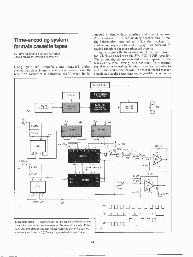
menred in simple data -recording and control systems.
Time -encoding system Also shown here is a rudimentary decoder circuit, andthe information required to utilize the markers for
formats cassette tapes controlling any cassette's stop, play, fast forward orrewind functions for more advanced systems.
by Fathi Saleh and Benham Bavarian Figure 1 a gives the block diagram of the tape format -Abadan Institute of Technology, Abadan, Iran ter, which was used with the JVC MC -1820R recorder.
The timing signals are recorded at the expense of onetrack of the tape, leaving the other track for monaural
Using operational amplifiers and standard digital sound or data recording. It might have been possible toelements to place 1 -minute markers on a stereo cassette add a thin head to the recorder in order to record markertape, this formatter is extremely useful when imple- signals and at the same time make possible two -channel
CLOCK (5 kHz)
DISPLAY4 -BIT EINARY
COU VIER
PARALLEL -TO -SERIAL
CONVERTER
TIMER(1 MINUTE)
DECADECOUNTER
SHAPINGCIRCUIT
(a)
10µF
1.5 MS2
560 k525V
7 6
555
11
0.005µF
_EH
(b)
2 3
82 1(2
27 kS2
7 6
555
2 3 14
5V
5V 5V
90Sh 7490
A OA Og Oc
0,, 0, 0. 0 0, 0 0. 0
NS74151
4 x LED
2
147400
5 -kHz CLOCK
1. On your mark . . . Tape encoder (a) places time markers on onetrack of a two -track cassette tape at 60 -second intervals. Pulsesfrom 555 step decade counter, whose output is converted to a BCDequivalent each minute (b). Timing diagram details operation (c).
27 kL2
27 kSl
120 kS2
0TAPE
3
2.2 kS2
270 kS2
5V
Al741
-5 V
+5 V
A2
741
120 kS2 -5 V
0 0 0 0 1 0 1 1 1
0(c)
0TORECO RDINGHEAD
41

data recording, but this was not tried.As shown in Fig. 1 b, the recording system uses a 555
timer to generate a pulse every 60 seconds, two 7490decade counters that are stepped by the timer to yieldrequired 8 -bit patterns, eight light -emitting diodes tomonitor the number generated, a parallel -to -serialconverter (74151) that is clocked at 5 kilohertz by asecond timer, a 4 -bit counter (7493), and shapingcircuitry.
Pulses emanating from the 1 -minute timer advancethe 7490s. The output of these devices is introduced tothe 74151, which is being clocked at a 5 -kHz ratethrough the 7493. The output of the 74151, after passingthrough a NAND gate, appears as shown in the timingdiagram (Fig. lc).
Recombining the 5 -kHz clock with other summing -circuit (A1) signals yields an output at A2 having a 50%
duty cycle. This output returns to a logic 0 when theoutput from the 74151 is a logic 1 and moves high for alogic 0 output from the 74151. The signal is a two -digitbinary -coded -decimal character which advances from 0to 60 minutes. The return -to -zero format is used here sothat one may differentiate between the zero -state andthe no -signal levels. This format also simplifies thedesign of the decoding circuits.
The playback (decoder) circuit is shown in Fig. 2. Theblock diagram (Fig. 2a) shows a complete controlsystem, but the system, although straightforward,encompass more circuitry than can be shown here.
The basic decoder is shown in Fig. 2b. Passing throughthe shaping circuit is the output from the tape recorder.This input signal is compared with a 1.2 -volt reference atC1, enabling the original bit pattern recorded to berecovered at its output. Meanwhile, the original clock
TAPE
(a)
FROMPLAYBACKAMPLIFIER
0
0
0
( c )
SHAPINGCIRCUIT
1.8 kE2
0.02µF
SERIALTO
PARALLELCONVERTER
PLAY BACKWARD: X > YPLAY -.STOP: X - Y
PLAY FORWARD: X < Y
10 kt2 ®
101(2
741
C2
BITCOMPARATOR
3.9162
1N914
1N914
Ct
741
5V
1.2 V(REFERENCE)
0
1.2 V(REFERENCE)
0
2
10
ANALOG-TO -
DIGITALCONVERTER
DISPLAY
7448
13a
SETTING
14 x ('47400)
12 3 'W
16
390 E212
10 390 E211
2
10C
7448 d
`AN
fj1D08-4AA-15 390 E2
14
3
12
0
9
15
14
0.1µFi
1 kE2 C34- 1
741
47400
rm. 3
ENABLESIGNAL
2. . . . Get set, receive. Complete control system would be imple-mented in straightforward manner (a). Rudimentary decoder, whichincludes only shaping circuit, serial -to -parallel converter and BCD -to -seven -segment circuits (b), performs operation essentially inverseto one at transmitter, as timing diagram confirms (c).
42

pulses are regenerated at C2 by comparing the rectifiedIs and Os of the bipolar return -to -zero input signal withthe 1.2-v reference. The bit pattern output from CI isconnected to the 74164 serial -to -parallel converter,which is stepped by the output of C2.
Thus the output of the 74164 is a binary -coded -
decimal equivalent of the marker -input's value. Theseven -segment displays that follow indicate the time, inminutes, corresponding to the last marker detected. 0
Digital logic multipliespulse widthsby N. Bhaskara RaoU.V.C.E, Department of Electrical Engineering, Bangalore, India
Using logic elements to multiply the width of incomingpulses by a value selected by the user, this circuit issimple to build and provides a higher accuracy -to -costratio than its analog counterpart. It should therefore findnumerous uses in synchronous systems, and although itsprime function is to provide a multiplication factor ofgreater than unity, it can generate smaller values as well.
The figure will help make circuit operation clear. Themultiplication factor is selected by presetting two74S192 down counters, A, and A2. Initially, counter A,is set to a value, M; A2 is preset to a second value, N; A3is zero; and the Q output of flip-flop A4 is high.
An incoming pulse of width T, (the signal to bemultiplied) switches on the 7408 AND gate and enables
A3 to count to a number determined by fl, which isderived from an external clock having input frequency f.Thus, at the end of the pulse, the counter contains thenumber fiTI. Note that f, = f/M.
When the trailing edge of the pulse arrives, A5 istriggered and presets A6 with the number contained inA3. Meanwhile, A4 is cleared (Q = 0) by A5, and the OR
gate is thereby activated so that counter A6 can initiatecounting from its preset value. Note that A6 is driven byA2, the divide -by -N down counter, and that f2 = f/N.
The time taken for A6 to reach zero from its presetvalue is thus T2 = (f,/f2)T1 = (N/M)T,. At thistime, the output from A;'s borrow port clears A3 andpresets the flip-flop. Therefore the time between theflip-flop's move to logic 0 (at the trailing edge of theinput pulse) and the time its Q output moves high againis T2.
The output signal is not derived until the input pulse'strailing edge arrives. The multiplication factor, N/M,can thus be set to any value greater or less than unitybecause the conversion is carried out after a delay.Needless to say, f should be much greater than T, foraccurate pulse -width multiplication.
ENO
EXTERNALCLOCK 4
M
151 11 101 91 IT-.A B C D LOAD
DATA
COUNT BORROW13
DOWN AlM
745192UP -DOWN COUNTER
N
151 4 .1 91 11
DATA
A3
N
74S192
DOWN COUNTER
2
f1
3
'47408
2D3
5V
4f-19
1
A, A2
A5
74121
ONE-SHOT30 ns
2.3
RESET
A3
74S90
UP COUNTER
A B
12
.111
'4 7432
-ED1-2 43
9
5
8 11
10 9
DATA
A674S192
DOWN COUNTER
13
6 7404
OUTPUT
-0A4
CLR 7470 P
FLIP-FLOP
ENO
T2
Width multiplier. Circuit has no analogelements. Multiplication factor is determinedby ratio of N to M, set by user. A6 is preset to
f,T,; stepped to zero at f2 rate, it signals
flip-flop. Time between state changes of flip-flop is T2 = (N/M)T,.
43

Negative -output regulatortracks input voltageby Gil MarosiIn tech Function Modules Inc., Santa Clara, Calif.
By using an astable multivibrator in a flyback arrange-ment to develop negative voltages from positive ones, thisregulator ensures that its output tracks the input, suchthat Vo = - Vhi. The voltage -controlled circuit requiresonly three active devices, all of them transistors.
Q1 and Q2 form the free -running oscillator, as shownin the figure. With Q2 on, the V1,, voltage is impressedacross resistor L, causing the current through L toincrease linearly. The peak value of current reachedbefore Q2 turns off will be directly proportional to themagnitude of the output voltage developed across capac-itor C4.
During the time the current through the inductorincreases, no voltage can be developed across C4 becausediode D is back -biased. When Q2 switches off, however,the collector voltage drops from Vi., and the capacitorcharges to a negative voltage. This occurs because thecharging current through the coil makes D turn on,
thereby causing a negative voltage at the output.The field across L then begins to collapse and D is
biased on, placing the output voltage (V. + Vd) acrossL, where Vd is the diode drop. The current through Lmust then fall linearly to zero. This completes one cycleof the flyback operation.
The input voltage is next compared with the outputvoltage at the summing node, at the base of Q3. Thistransistor amplifies the voltage difference and trans-forms it into a current that is used to control Qz'sturn -on time. Thus if Vo, should fall, the control currentwill act to increase the on time of Qz, thereby increasingthe peak current through L and so raising the outputvoltage. This analysis assumes that Vi0 emanates from astiff source-that is, an increased current demand willnot cause a drop in V10 because of an increased voltagedrop across the source's internal impedance.
Without Q3, the load regulation would be directlyproportional to a change in load current (IL) and so a10% change in IL would cause a 10% change in loadvoltage VL. Q3 ensures that such a change in IL causesonly a 0.2% change.
Component values are given for a circuit that operateswith an IL = 20 milliamperes, a V. = -5 volts, and anastable multivibrator operating at 50 kilohertz (r = 20microseconds). Equations are given in order to facilitatethe design of regulators for specific parameters.
a,2N2907
1N4148
VIN
0,Ci 2N2907
7,100 pF1,000 pF
141N4148
C4
668 12 2 k.1?. R, C220µF
210 12, 712 pH
D3
2N2222
c,0.1AF
R4
rivoi, Vd]L= 4 IL
2 71 - T210r1amA) 5,s,/ T2 IL
C2
L 81,
ClT2=
5.6 1(11 200120.7 R2 12 Vol C3 - 64 C4 lAVol
R5FINE ADJUST
4.31(127.1
-0.7 1%441-0.8-= 62 -2. R32 C1 Ip IL
V0 + 0.7 VIN -0.70 4 =
1 mA 1 mA
Flyback follower. Regulator uses astable multivibrator 01-02 and inductor to generate negative output voltages from positive inputs whilealso ensuring that = Differential amplifier Q3 serves to develop feedback control voltage to readjust on time of 02 and thus voltagedeveloped across L and C4 when V.., # - V,. Component values are given for IL = 20 mA, V. = -5 V, and f = 50 kHz.
44

Controller selects mode formultiphase stepping motorby Oldrich PodzimekElectrical Engineering Research InsTitute, Prague, Czechoslovakia
Offering a selection of the most common steppingmodes, these circuits are an inexpensive solution to theproblem of torque control in four- and five -phase motors.The mode can be changed simply by the flip of a switch.
The basic circuit is the same for either stepping motor.It consists of a 4 -bit binary -coded -decimal counter, aBCD -to -decimal converter, and several gates that serve asphase detectors.
The four -phase controller is shown below. The 74193counter advances with each input -clock pulse at afrequency determined by individual requirements. Note
that the 74193 can count up or down and so may be usedto step the motor in the opposite direction if desired.
As the counter increments or decrements, the outputof the 7442 4 -to -10 -line decoder switches in a mannerdependent on switch S. If S connects port A' of the 7442to the A port of the 74193, the decoder's output willmove from 0 to 7 in sequence. Otherwise, the output willswitch to even values every other count (S connected tologic 0) or switch to odd values (S connected to logic 1).
A combinational logic circuit using gates G1-G4converts the 7442's output to phase information in orderto drive the motor. As can be seen in the truth table,either one or two windings of the motor will be active atany given time.
The motor will step most smoothly when S is connect-ed to A. When S is connected to L, the step angle will bedoubled, and only one of four motor windings will beexcited at any given instant, thereby improving the effi-ciency of the step operation for a given torque. Note thatwhen S is in the H position, the step angle will be the
74193 7442
912
08
CLOCK5 COUNT
7UP
3 6
65
54
8144
34
CLOCK4 COUNT
2DOWN *
A. 15 1A
2-5 V -0
11/2 x 7410
2
13
4
9
10
2
13
12
15-
CO -
12
COUNTER OUTPUTA L H
PHASEZ
PHASEZ
PHASE,
ZA B C D 1 2 3 4 1 2 3 4 1 2 3 4
0 0 0 0 OR 1 1 0 0 0 0 1 0 0 0 0 1 1 0 0 1
1 0 0 0 OR 1 1 1 0 0 1 1 0 0 0 0 1 1 0 0 1
0 1 0 0 OR 1 0 1 0 0 2 0 1 0 0 2 0 1 1 0 3
1 1 0 0 OR 1 0 1 1 0 3 0 1 0 0 2 0 1 1 0 3
0 0 1 0 OR 1 0 0 1 0 4 0 0 1 0 4 0 0 1 1 5
1 0 1 0 OR 1 0 0 1 1 5 0 0 1 0 4 0 0 1 1 5
0 1 1 0 OR 1 0 0 0 1 6 0 0 0 1 6 1 0 0 1 7
1 1 1 0 OR 1 1 0 0 1 7 0 0 0 1 6 1 0 0 1 7
Z = SWITCHED OUTPUT OF 7442 (DECIMA_ EQUIVALENT)
PHASE 4
PHASE 3
PHASE 2
PHASE 1
1. Multimode. Step controller uses up -down counter, decoder, and logic to control excitation of four -phase motor windings. Switch S selectsone of three possible operatinc modes, ranging from smooth -stepping to high -torque.
45

74192 7442
CLOCK 5 COUNTUP
CLOCK COUNTDOWN
7
2 1
A -
L0
15 A'
rn
8 10
7 r
6 r 7
5 6
4 /5.4
2 1 0
5 x 7430
3 65 PHASE 545
2
3 G4 PHASE 44
3 G3 PHASE 34
5
3 PHASE 245
23^8PHASE1
5
2
2
4
C UNTI IA UTPUTA L 14
PHASEZ
PHASEZ
PHASEZ
A B C D 1 2 3 4 5 1 2 3 4 5 1 2 3 4 5
0 0 0 0 1 1 0 0 0 0 1 1 0 0 0 0 1 1 1 0 0 1
1 0 0 0 1 1 1 0 0 1 1 1 0 0 0 0 1 1 1 0 0 1
0 1 0 0 0 1 1 0 0 2 0 1 1 0 0 2 0 1 1 1 0 3
1 1 0 0 0 1 1 1 0 3 0 1 1 0 0 2 0 1 1 1 0 3
0 0 1 0 0 0 1 1 0 4 0 0 1 1 0 4 0 0 1 1 1 5
1 0 1 0 0 0 1 1 1 5 0 0 1 1 0 4 0 0 1 1 1 5
0 1 1 0 0 0 0 1 1 6 0 0 0 1 1 6 1 0 0 1 1 7
1 1 1 0 1 0 0 1 1 7 0 0 0 1 1 6 1 0 0 1 1 7
0 0 0 1 1 0 0 0 1 8 1 0 0 0 1 8 1 1 0 0 1 9
1 0 0 1 1 1 0 0 1 9 1 0 0 0 1 8 1 1 0 0 1 9
Z = SWITCHED OUTPUT OF 7442 (DECIMAL EQUIVALENT)
2. Multiphase. Controller for stepping five -phase motors is similar to that for four -phase case. Five 5 -input NAND gates and some additionalwiring are the only new changes required for enabling up to three phases of a motor to be excited simultaneously.
same as in the preceding case, but two motor windingswill be active at any time, power input will be doubled,and 41% greater torque will be obtained.
A similar circuit suitable for stepping five -phase
motors is shown above. In this case, either two or threephases of the motor are excited simultaneously. Thiscircuit can be extended to solve a general m -phase motorproblem.
Op amps and counter formlow-cost transistor curve tracerby Forrest P. Clay Jr., Clarence E. Rash, and James M. WaldenOld Dominion University, Department of Physics, Norfolk, Va.
For a curve tracer, this relatively simple circuit isunusually inexpensive. Used to test small -signal bipolartransistors as well as junction diodes, it generates the
waveforms needed to display or plot their characteristiccurves on an oscilloscope or X -Y plotter, interfacingdirectly with either. Operational amplifiers, one transis-tor, and a single binary counter are the only activedevices needed.
Central to the circuit is a current generator made upof an op amp driven by the counter. It supplies eightlevels of base current in sequence to the transistor undertest. Op amps Al and Az, with the aid of the RI-It2-C1timing network, initially produce both square and trian-gular waves at test points A and B (TPA and TPB),respectively. S1 selects the waveform frequency-either
46

+15 V
R, 18 MS2 MYLARe'VA-01z,S1 CI 0.47p F
0.1 Hz-vvs,-0
R2 1 kHz
2k52
-15 V f R320 kS2
2
-15 Vnpn
S2c
R15
10 kS2
H,6
10 kS2
R17
10 kS2
(a)
415 Vpnp
TPB
10 k52
R19
10 kS2
R18
10 k2
TRIANGLEWAVEOFFSET
- CONTROL
R5
TPA
+15 V
R7
3 kS2
2N22226
3 k12
1 k2
1N4148
1 u2
0
R21
100 kS2
R2O
+15 V
\ 15V
pA759 0
TPE
TPC0
15
S2
+15 V
CD43151
R1,3
200 k52R9
100 kS2
14 R9
9 50 kS2
1.151412113.
R,,
27 kS2 R13
10 kS2+15 V
A3
-15 V
R12
10 kS2
R 5 k2
npn
pnpTPE
TPO 0 0
-15
SOCKET FORTRANSISTORUNDER TEST
Rc tt
100 2 1
R23W 10 kS2
R25
5k52
10 k52V4/1,
A7
R24
100 kS2 IMA
R26 R27
100
100 kS2ss
R29
100 k52
A, -A4, A6 -A9: %7L084
Prol°
X-AXIS OUTPUTR28 npn
Rat
R30 10 kS2
10 k2MA,
Vo AB
R32 5 kS2
-÷-
pnp(3 S 2e
04?) -4) Y-AXISn" OUTPUT
(b)
2.0
1.6
E
= 0.8
0.4
2N3053 (npn)
RETRACE
-"-- TRACE140
120
100
80
60
40J..- 20_1_
0 02 4 6 8 10 12 VcE (V)
Z:e
2.0
1.6
a 1.2E
= 0.8
0.4
0
RETRACE
2N2907A (pnp)
140
120
100
80
60 -f
40
200
2 4 6 8 10 12 VcE (V)
Current family. Tracer produces set of eight curves of collector current vs colector voltage from npn or pnp transistor under test. Diodes mayalso be checked in circuit's pnp-transistor mode (a). Representative curves are plotted using X -Y recorder (b). Note temperature effects seenon the retrace portion of curves for higher values of lb and lc.
1 kilohertz for output onto an oscilloscope or 0.1 hertzfor plotting with an X -Y recorder.
The waveform at TPA is then shaped by Di-R5 orD2-R6 into a clock pulse suitable for the 4516 binarycounter. The signals emanating from the Q., Q131 and Qcports of the counter, when fed into a binary -weightedsummation network (R8-R11), produce an eight -stepstaircase waveform at the output of A3 or A4, dependingupon whether a pnp or npn transistor is under test. Theactual base current value is determined by appropriateselection of R21. The collector current can be calculatedfrom l,, =
Both the collector -biasing voltage for the transistorunder test and the linear -deflecting voltage for theX-axis output to the scope are derived from the trianglewave. The first voltage is obtained by using Sec and R,6,which permit the proper dc component to be added tothe triangle signal.
Note that the Y axis is stepped at one eighth of therate at which the X axis is scanned. Thus, if thesampling rate is 1 kHz, each of the eight current levels isswept at a rate 125 Hz, well above the rate at whichflicker is detectable on a scope.
The circuit is easy to use. Simply place ganged switchS2 into whichever position is correct for the type oftransistor being measured (npn or pnp); place the tran-sistor into the test socket; and apply circuit power. Totest a diode, insert its anode and cathode leads into theemitter and collector sockets, respectively, and put S2 inthe pnp mode.
Figure lb shows two representative families of curvesthe circuit produced on an X -Y recorder for the twotypes of bipolar transistor. 0
47
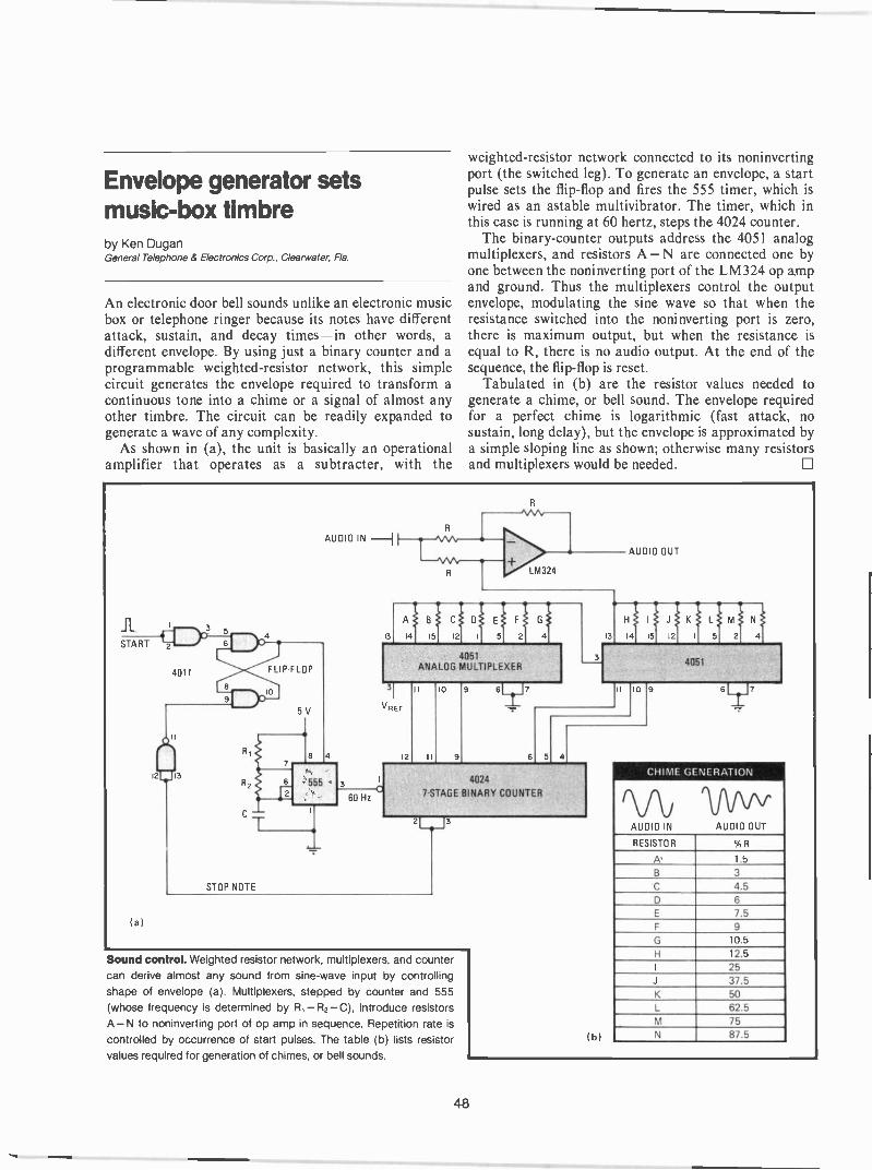
Envelope generator setsmusic -box timbreby Ken DuganGeneral Telephone & Electronics Corp., Clearwater, Fla.
An electronic door bell sounds unlike an electronic musicbox or telephone ringer because its notes have differentattack, sustain, and decay times-in other words, adifferent envelope. By using just a binary counter and aprogrammable weighted -resistor network, this simplecircuit generates the envelope required to transform acontinuous tone into a chime or a signal of almost anyother timbre. The circuit can be readily expanded togenerate a wave of any complexity.
As shown in (a), the unit is basically an operationalamplifier that operates as a subtracter, with the
weighted -resistor network connected to its noninvertingport (the switched leg). To generate an envelope, a startpulse sets the flip-flop and fires the 555 timer, which iswired as an astable multivibrator. The timer, which inthis case is running at 60 hertz, steps the 4024 counter.
The binary -counter outputs address the 4051 analogmultiplexers, and resistors A -N are connected one byone between the noninverting port of the LM324 op ampand ground. Thus the multiplexers control the outputenvelope, modulating the sine wave so that when theresistance switched into the noninverting port is zero,there is maximum output, but when the resistance isequal to R, there is no audio output. At the end of thesequence, the flip-flop is reset.
Tabulated in (b) are the resistor values needed togenerate a chime, or bell sound. The envelope requiredfor a perfect chime is logarithmic (fast attack, nosustain, long delay), but the envelope is approximated bya simple sloping line as shown; otherwise many resistorsand multiplexers would be needed. El
(a)
AUDIO IN -I
13
1
14
VREF
12
AB1 COEF G
LM324
15 12 1 5 2 4
4051ANALOG MULTIPLEXER
10 61 17
13
AUDIO OUT
HI J!K1LSM N
14 15 12 1 5 2 4
4051
10 9 6 7
6
4e27 -STAGE BINARY4 COUNTER
3
Sound control. Weighted resistor network, multiplexers, and countercan derive almost any sound from sine -wave input by controllingshape of envelope (a). Multiplexers, stepped by counter and 555(whose frequency is determined by R, -R2- C), introduce resistorsA -N to noninverting port of op amp in sequence. Repetition rate iscontrolled by occurrence of start pulses. The table (b) lists resistorvalues required for generation of chimes, or bell sounds.
5 4
(b)
CHIME GENERATION
AUDIO IN AUDIO OUT
RESISTOR %R
A, 1.5
B 3
C 4.5D 6
E 7.5F 9
G 10.5
H 12.5
I 25
J 37.5K 50
L 62.5M 75N 87.5
48

VCOs generate selectablepseudo -random noiseby James D. LongAerojet ElectroSystems Co., Azusa, Calif.
In this circuit, several voltage -controlled oscillators,whose outputs are summed in order to generate a suit-able feedback voltage to their inputs, are used to gener-ate pseudo -random noise over band limits that can beselected by the user. Using vcos makes possible a trans-fer function that is closer to the ideal and ensures thatthe circuit has better amplitude -versus -temperaturestability than conventional generators, which rely onspecial and often expensive diodes to produce noise overa wide band. This generator will be suitable for manyapplications, producing random noise over a bandwidthof three octaves, with a crest factor (ratio of peak to trueroot -mean -square voltage) of three.
The key to circuit operation is to generate a randomfeedback voltage to the bank of vcos so that their outputfrequencies vary randomly, thus in effect producingnoise. This task can be accomplished with the circuitshown in the block diagram. Note that the frequency ofthe feedback (modulating) voltage is unimportant solong as the maximum modulating frequency is less thanany oscillator's output frequency.
A single vco usually retains its linear input -voltage-
to -output frequency characteristic over less than one
octave. The three -octave bandwidth can be realized byoperating several vcos over adjacent frequency bands(staggered tuning). Low-pass filters remove the higher-
order harmonics contained in the square -wave outputs ofthe oscillators and the signal appearing at the output ofthe summing amplifier is similar to random noise.
The feedback signal required to generate the randomnoise is derived by first combining the output of all vcosin a resistive summing network. The output from thesummer is a signal that contains zero crossings occurringat random intervals.
A divide -by -64 circuit detects threshold crossings andbrings the summer signal down to a frequency rangeconsistent with the requirement that the highest modula-tion frequency be much less than the total outputfrequency of the vcos. A narrowband (Q=5) LC filterthen smooths these random amplitudes into a continuoussignal for the vcos' inputs. With proper scaling factorsprovided by the amplifier, the desired range of randomfrequencies can be generated.
Each vco is biased to its appropriate geometric -meanfrequency and operates there if the modulation ampli-tude is zero. Attenuators al through a allow indepen-dent control of the deviation range of each vco, and theadjustable limiter permits control of the peak deviationfrequency. The function of the adjustable limiter is toensure that the oscillators do not deviate beyond theirprescribed frequency bands. If the vcos' band edges arealigred so that no overlaps nor gaps occur betweenadjacent bands, the distribution of frequencies at theoutput of the summing amplifier will be uniform. Align-ment of the band edges is not difficult.
VOLTAGE -CONTROLLED OSCILLATORS: MOTOROLA MC1648OTHER
MODULATINGGENERATORS
LOW-PASS
S, ATTENUATORa1
DUAL VCO1
FILTER 1
LOW-PASSFILTER 2
LOW-PASSH ATTENUATORa2
DUAL VCO2
FILTER 3
SUMMING
OUTPUTSIGNAL
LOW-PASSFILTER 4
AMPLIFIERLOW-PASS
ATTENUATOR DUAL VCO,i FILTER 5
ADJUSTABLE LOW-PASSa3 3
LIMITER FILTER 6
LOW-PASSFILTER n-1ATTENUATOR
anDUAL VCO
n
ILOW-PASSFILTER n
AMPLIFIERNARROW:
BANDFILTER
64DIGITALDIVIDER
RESISTIVESUMMER
In the noise. Method for generating noise uses summed outputs of voltage -controlled oscillators to generate feedback voltage that variesrandomly with time, thereby causing frequencies of oscillators to vary in the same manner. System provides uniform noise output over threeoctaves, with a noise -voltage crest factor of three. Generator can produce other waveforms if appropriate modulating signals are applied.
49

This generator can produce signals other than noise. will generate a swept -tone output. If the vco has anSwitch SI may be used to apply any modulating signal to inhibit input, it can be selectively activated so thatthe vcos' inputs. For example, a sawtooth input signal pulsed tones can be generated.
Multiplier, op amp generatesine for producing vectorsby Jerald GraemeBurr -Brown, Tucson, Ariz.
To compute trigonometric functions of the kind thatproduce a vector from its X and Y components, a systemneeds to be supplied with signals that are proportional tothe sines of the applied X and Y dc -voltage inputs. Amultiplier, operating as a signal squarer, and an opera-tional amplifier, serving as a subtracter, will process theX or Y component more simply than other circuits nowgenerally used. With these components, the desiredwaveform response for either input-the positive half ofa sine function-can be approximated to within 5% of aperfect waveform, a value well within the limits thatyield good computational accuracy.
Using the multiplier and the op amp to generate thesinusoidal transfer function is much easier than usingdiodes in complex circuits to synthesize the nonlinearresponse by producing a piecewise-linear approximation.Also, this circuit produces the sine response over therequired - 90° to + 90° quadrant using one less multi-plier than existing analog circuits,' which generate theapproximation by means of a long mathematical seriesor an equivalent method.
The circuit shown in (a) processes the dc input voltagethat corresponds to either the X or Y component of thevector. The BB4213AM has a transfer function of G =X' Y' /10, where X' and Y' are the inputs; it is made tosquare the input voltage, e,, when the X' and Y' portsare connected. The output of the squarer is then intro-duced into the inverting port of the BB3500 op amp,with e, fed to its input, so that:
eo = 3.86 (e;-ice) (1)
But Eq. 1 can be expressed by:
eo 10 sin (for), 0< e, < 10 (2)
which results from a simple series approximation. Thiscan be confirmed in the actual output -versus -input volt-age plot (b). Equation 2 may be scaled for other input -voltage ranges by changing the gain of the op amp.
Note that term 2 in Eq. 1 (representing the actualoutput response) has a second -order exponent, whereas aTaylor -series, which would yield a closer approximationto a sine wave, would have a third -order exponent ofconsiderable magnitude in term 2. In spite of this differ-ence, however, Eq. 1 is reasonably accurate as evidencedby the error -curve plot (c), which peaks at 4% of fullscale. Dominant distortion is related to the second and
e,
X COM-PONENTORY COM-PONENT
(a)
13
0
(b)
CC
C/3
LLLL0
CC
0CCCCLLJ
(c)
ec,
TO VECTOR -PROCESSINGCIRCUIT
10.21(52 39.2 1(2
e. = 3.861e, - e,2/10) 10 sin (e,/10)7r, < e1 < 10
5 10 e, (V dc)
Coordinates. Squaring and subtraction (a) of input wave from itselfproduces a series approximation to a half sine wave (b). Two suchcircuits, given X and Y coordinates in the form of dc -voltage inputs,can generate output for systems suitable for computing vectors.Approximation error (c) for half sine is within 5%.
third harmonics that are present at the output.An additional error term of up to 1% is introduced by
the inherent nonlinearities in the multiplier circuit'stransfer function. The error introduced by the op amp,however, is negligible.
Rofitrences1. Burr -Brown, Model 4213 Product Data Sheet, PDS366, 1976.
50
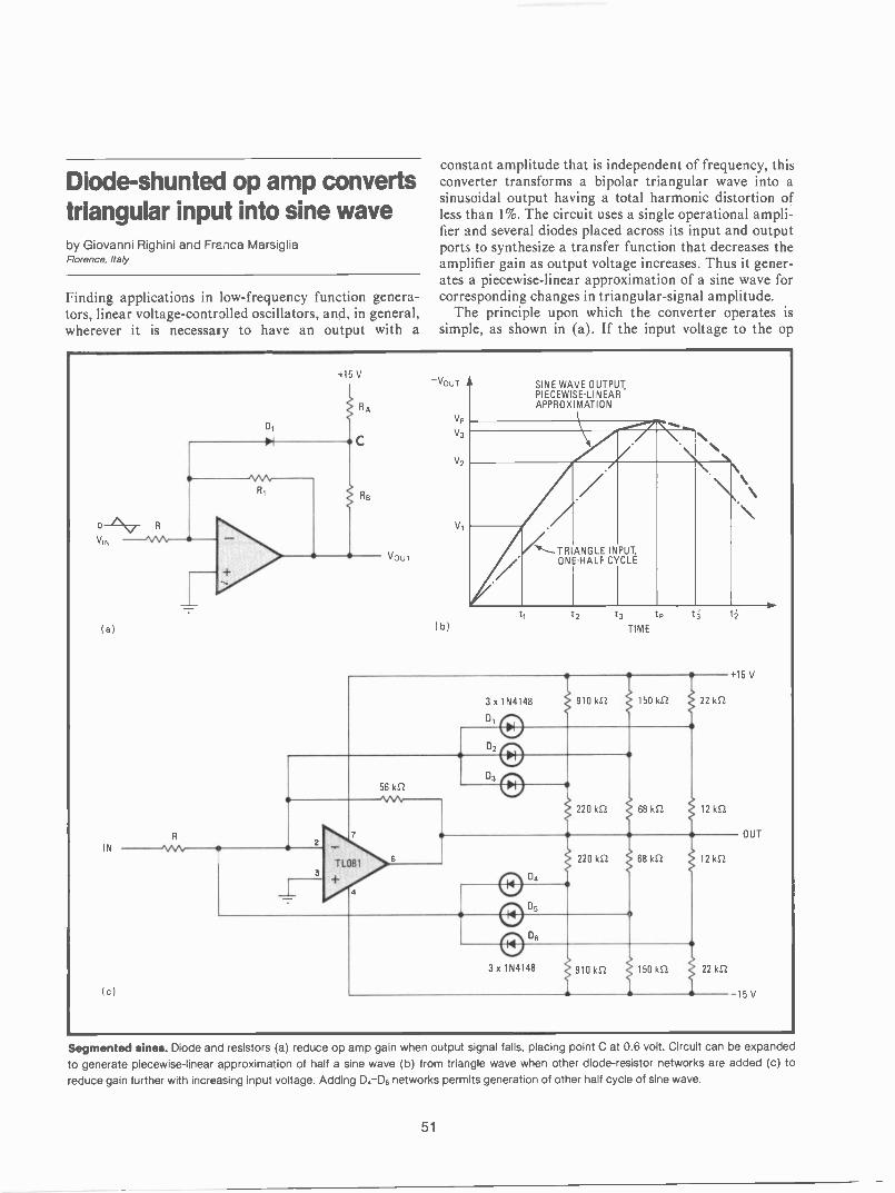
Diode -shunted op amp convertstriangular input into sine waveby Giovanni Righini and Franca MarsigliaFlorence, Italy
constant amplitude that is independent of frequency, thisconverter transforms a bipolar triangular wave into asinusoidal output having a total harmonic distortion ofless than 1%. The circuit uses a single operational ampli-fier and several diodes placed across its input and outputports to synthesize a transfer function that decreases theamplifier gain as output voltage increases. Thus it gener-ates a piecewise-linear approximation of a sine wave for
Finding applications in low -frequency function genera- corresponding changes in triangular -signal amplitude.tors, linear voltage -controlled oscillators, and, in general, The principle upon which the converter operates iswherever it is necessary to have an output with a simple, as shown in (a). If the input voltage to the op
(a)
N
( c)
+15 V
VouT
--VouT
VP
V,
(b)
SINE WAVE OUTPUT,PIECEWISE-LINEARAPPROXIMATION
56 k&2
2
TL081
3 x 1N4148
o
02 C)
0
1910 kSt 150 kS2 22 kS2
220 kS2 68 kS2 12 kS2
+15 V
220 kS2 68 kS2 12 kS2
3 x 1N4148 910 kS2 150k12 22 kS2
OUT
15V
Segmented sines. Diode and resistors (a) reduce op amp gain when output signal falls, placing point C at 0.6 volt. Circuit can be expandedto generate piecewise-linear approximation of half a sine wave (b) from triangle wave when other diode -resistor networks are added (c) toreduce gain further with increasing input voltage. Adding D., -D6 networks permits generation of other half cycle of sine wave.
51

amp is such that the output voltage is positive, diode D1does not conduct and the amplifier gain will be R1/R.But when a positive input voltage from the triangularinput is applied to the inverting port, the output will gonegative and DI will conduct when point C reaches athreshold value of -0.6 volt.
In effect, if the internal impedance of the diode isneglected so long as it is conducting, resistor 116 is inparallel with R1, and the amplifier gain is reduced toRIRb/(RI + Rb)R. The change in gain occurs at point V1on the transfer function (b).
By placing additional resistor -diode networks thatinclude D2 and D3 at the output of the op amp (c) and byselecting resistor values appropriately, the voltage atwhich conduction occurs for each diode can be set. So,for each progressive rise of the triangular voltage thetransfer function can be extended to points V2 and V3. Agood approximation to a half sinusoid can be obtained byusing four segments for every quarter of a (sine wave)period, as shown.
To process the negative -polarity portion of the trian-gular wave (which is required to generate the other halfof the sine wave), resistor -diode networks including D4,Ds, and D6 are placed in the circuit. Note that the diodeswill conduct in sequence as the op amp's output voltageexceeds the predetermined positive values.
The component values have been selected to producethree segments corresponding to end -point values ofIV = 4.35, =7.7, Iv31= 9.15. Vp is limited by the maxi-mum voltage of the input signal. Only resistors having atolerance of 5% or below should be used in this circuit, tokeep distortion to a minimum.
The gain of the op amp is most conveniently controlledby varying R and can be selected to handle a wide rangeof input voltages-from a few tens of millivolts to tens ofvolts. R should be about 1.8 kilohms for input voltages of1 v peak to peak and should be trimmed to minimizesine -wave distortion at the output.
The frequency response of the circuit will exceed 30kilohertz when the TL081 op amp is used. I=1
Open -collector logicswitches rf signalsby W. B. WarrenTRW Subsea Petroleum Systems Inc., Houston, Texas
The open -collector outputs of transistor -transistor logiccan provide a simple way of switching low-level radio -frequency signals and thus digitally selecting signalsources in test equipment or filters in a communicationsreceiver. With a 50 -ohm source and load, the rf attenua-tion through the switch at 10 megahertz is only 1.3decibels when the switch is active and greater than 40 dBwhen it is open.
Shown in (a) is the basic rf switching element. Whenthe logic control signal is low, the open collector outputof the NAND gate is high. Thus diode D1 is back -biased,D2 conducts, and the switch is turned on. The capaci-
tance of the open -collector output of the logic elementwill not affect circuit operation, since the reverse -biasedD1 prevents the element from shunting the rf path.
When the control signal is high, the open -collectoroutput is low and D1 conducts, forcing the dc voltage at
5V
(al
2V
Of
f4
5V
OPEN COLLECTOR
rf OUT
LOGIC--CONTROL
SIGNAL
0.1 pF
II
rt IN
2V
r(71)11pF
50pH
0 01 µFrf OUT
1
1N914
1N914
330 S2
3k12
5V
0.1 pF
0.01µF rf OUT#2
1N914
--"SAA/-1N914
330 ft -7-
I 5VT " PF
TTL INPUT °LOGIC 0 =
rf OUT #1 ILOGIC 1 =
rf OUT #2
(b(
2
5
3 kS2
10
6
SN7401
9
8
14
3 kS2
5V
Digital rf switch. Logic signal is capable of switching low-level radio -frequency signals without significant attenuation, if open -collectortransitor-transistor-logic element is used (a). Basic idea can easily be extended to single -pole, double -throw rf switch (b).
52
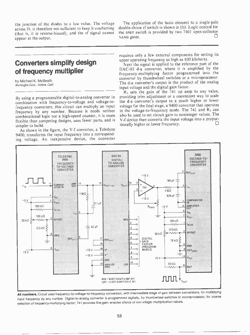
the junction of the diodes to a low value. The voltageacross DI is therefore not sufficient to keep it conducting(that is, it is reverse -biased), and the rf signal cannotappear at the output.
The application of the basic element to a single -poledouble -throw rf switch is shown in (b). Logic control forthe sPDT switch is provided by two 7401 open -collectorNAND gates.
Converters simplify designof frequency multiplierby Michael K. McBeathBurroughs Corp., Goleta, Calif.
By using a programmable digital -to -analog converter incombination with frequency -to -voltage and voltage -to -frequency converters, this circuit can multiply an inputfrequency by any number. Because it needs neithercombinational logic nor a high-speed counter, it is moreflexible than competing designs, uses fewer parts, and issimpler to build.
As shown in the figure, the V -f converter, a Teledyne9400, transforms the input frequency into a correspond-ing voltage. An inexpensive device, the converter
requires only a few external components for setting itsupper operating frequency as high as 100 kilohertz
Next the signal is applied to the reference port of theDAC-03 d -a converter, where it is amplified by thefrequency -multiplying factor programmed into theconverter by thumbwheel switches or a microprocessor.The d -a converter's output is the product of the analoginput voltage and the digital gain factor.
R3 sets the gain of the 741 op amp to any value,providing trim adjustment or a convenient way to scalethe d -a converter's output to a much higher or lowervoltage for the final stage, a 9400 converter that operatesin the voltage -to -frequency mode. The 741 and R3 canalso be used to set circuit gain to noninteger values. TheV -f device then converts the input voltage into a propor-tionally higher or lower frequency.
(IN
-5 V
20 kE2
+5 V
TELEDYNE9400
FREQUENCY -TO -VOLTAGECONVERTER
COMPAR-ATOR IN
v s
VRE F
'BIAS
OFFSET
GNU
0
AMPOUT
REFo,
15
1 ME2
3
0.1µF
47 pF
+15 V
-15 V
73
16
12
13
DAC-03
DIGITAL -TO -ANALOGCONVERTER
NI
V
V
GND
ANALOGGNU
VOUT
MSB
LSB
4 3
2
+15 V
741
-15 V
0
3
4
9
0
0
0
0
0
MSB = MOST SIGNIFICANT BITLSB = LEAST SIGNIFICANT BIT
RGAIN
50 kE2
DIGITALGAINFACTOR(PROGRAM-MABLE)
+5 V
5
180 pF
1 ME2
820 pF
-5 V 12
100 kS2
510 kit
10 1(11
10 kilo
9400
VOLTAGE -TO -FREQUENCYCONVERTER
REEDuT
COMPARATORIN
AMPLIFIEROUT
Vss
REF
BIAS
OFFSET
GNO
OUTGND
OUT
tOUT
All numbers. Circuit uses frequency -to -voltage -to -frequency conversion, with intermediate stage of gain between conversions, for multiplying
input frequency by any number. Digital -to -analog converter is programmed digitally, by thumbwheel switches or microprocessor, for coarse
selection of frequency -multiplying factor; 741 provides fine gain, enables choice of non-integer multiplication values.
53

Zero -sensing counter yieldsdata's magnitude and signby Gary A. FrazierRichardson, Texas
Upon sensing when an ordinary up -down counter isabout to count down through zero, this circuit reversesthe direction of the count to enable it to express anegative number by its magnitude and sign, instead of bythe more usual but less convenient 2's complement. Thecircuit similarly represents positive integers, making iteasy for any stored value to be handled directly by suchdata -system devices as digital -to -analog converters ormicroprocessors.
The unit shown in the figure has been found particu-
OVERFLOW
123
C1 -C,, 74192 (BCD) OR 74193 (BINARY)
CLUP OCK
A
C11
C
BORROW
CLEAR
CLOCK0 DOWN
12
CARRY Oa [lb a, ad BORROW
C2 CLEARCLUP OCK CLOCKABC D DOWN
5
12 0 3
15
2 6
10
7
9 4
13Q
CARRY O. a, 0, 0,1 BORROW
CLOCKUP
Cl
CLOCKDOWN
CLEAR
5
6
4
Y 7400
4 5 9
DATA
1/47400
10
%7400
zl 13
14
14
14
3 al.1/47486 2
'47400
3
5V
4 120 1
K C J
1/2
74107 CLEAR
O
larly useful in a digital -averaging application. Data issampled during an interval in which the ADD/grrB line istoggled at some frequency,'which in this case varies withtime, as shown. Any data in phase with the ADD/TITBsignal will accumulate in the n -stage counter (count-upmode), and digital noise will be averaged out (sub-tracted). The output of the counter is sampled at the endof the data -collection interval.
If the contents of the counter should ever decrease tozero, a borrow pulse is generated by the most significantcounter, C,,, and toggles the flip-flop. In turn, the NANDgate connected to the clock -up port of C1 is enabled. Inthis way, the output of the counter is mirrored about 0,as shown in the timing diagram, and is equal to theabsolute value of the difference between the number ofthe add -to and the subtract -from counts. The sign bit isset each time the data actually drops below zero.
Note that when using the up -down counter, it isnecessary to keep the counter cleared while the BORROWis low to avoid difficulties should the clock -up linesuddenly become disabled while the clock -down line isactivated. Otherwise, a decrement will take place. Thefrequency and symmetry of the ADD .113 waveform isarbitrary so long as the counter does not overflow on anyhalf cycle of a sampling interval. 1=1
About face. Circuit inhibits up -down counters C1 -C, from decre-menting below zero, instead forcing them to count up and mirror theresult of a negative -number addition in binary form. A negative -signbit is also generated. Thus, all numbers are suitable for directhandling by a d -a converter or other data -system device.
ADO/SUBTRACT SIGN CLEAR
ADD/SUBTRACT
COUNTS
SIGN
11VALUE OF COUNTER
TRUE VALUE OF DATA
Demand -switched supplyboosts amplifier efficiencyby Jerome LeinerLoral Electronic Systems, Yonkers, N. Y.
The efficiency of high -power audio amplifiers operatingin class B will be improved by up to 80% at low powerlevels if the supply voltage can be switched from a lowto a high value as the power demands on the amplifierincrease. Using the automatic -switching circuit de-scribed here ensures a lower heat dissipation than wouldbe possible with an amplifier that delivers a low -poweroutput from a single high -voltage supply, which is the
54

-1 v
-14.3 V
-20 V
Qt -Q2 ON
03-Q, ON
-15 V
r
10A1/46
I SE9403L
1N3879
a,
I SE9403
-30 V
04
10 S2
loutTO SCOPE
EoutTO SCOPE
High efficiency. Audio power amplifier switches from Darlington pair 0,-02 and low -voltage supply to 03-04 and high -voltage supply onlywhen power output demands increase. Circuit thereby eliminates the need for amplifier to dissipate excessive heat, a condition that occurs
when an amp with a single high -voltage supply is used to process a low -amplitude input signal.
most common situation. The increased efficiency of thispower amplifier can produce considerableweight and size and also reduces the amplifier's heatsink requirements.
The amplifier is designed to switch from the low- tothe high -voltage supply as the audio signal level passesup through the low -voltage supply level. The switchoveris made with virtually no perturbation in the outputcurrent up to as high as 25 kilohertz. At higher speeds,any waveshape distortion can be reduced by implement-ing negative feedback around the amplifier. Both supplyvoltages can be derived from one source, with the lowvoltage taken from a selected tap on the power trans-former.
Several circuit configurations were tried, among thema cascaded emitter follower, a series transistor configu-ration, and the parallel transistor arrangement shown inthe figure. The cascaded emitter follower and the seriesconfiguration performed adequately below 10 kHz. Athigher frequencies, however, the effects of carrier stor-age produced by the first two arrangements caused large
perturbations in the output current. The parallelarrangement finally adoptedproblem and appears to be the most useful at higherfrequencies.
For simplicity, the operation of one half of a comple-mentary -output stage (see figure) is described. A half -sine wave that swings from - 1 to - 20 volts is theinput -signal source in this case.
When the input level is at - 1 v, current flows throughD2, R1, and D. Thus the input base of Darlington pairQ,-Q2 is one diode drop lower than the base of Q3-Q4.As a result, Q,-Q2, which uses the - 15-v supply, is onand Q3-Q4 is off.
When the input signal reaches within one diode dropof the low -voltage power supply, D2 begins to turn offand Q3-Q4, which uses the - 30-v supply, starts to turnon. As Q3-Q4 moves into the linear region, Q,-Q2 beginsto turn off, so there is a smooth transition of current inthe load. Q3-Q4 stays on until the signal polarityreverses; when the signal passes through the low -voltagesupply level, QI-Q2 goes on and Q3-Q4 goes off.
Fast -acting voltage detectorprotects high -current suppliesby Jorges S. LucasEngeletro, Belo Horizonte, Brazil
Protecting a regulated, nonswitching power supplyagainst both short circuits and overvoltages can be diffi-cult, especially if the supply is to deliver high currents.Should either condition occur, this circuit will act quick-ly to protect the supply, and its load as well, by deacti-vatung the series or shunt pass element in the regulatorand thus forcing the output current and voltage to zero.
A typical high -current power supply (5 volts at 5
55

6A30 V --cam
2N3055
2N3055
1852
4.7 k1-2
C4
1 I
10 S2
BD139
BC141
100 nF
2N5064
BC141
0.112
1052
10v
680 Si
t -E' 2.2 V
741 TC
1 kS2
Vref
680 S2
4.7 kS2
1.5 k1-2
OUTPUT5V@ 5 A MAX
0, 02
1N4148
C,
10pF
1N4148
l
C327
12 kS2
02BC337
R2 R3
5.6 kS2
03
BC337
THRESHOLD
1N4148
Ra
18 kS2
3
R5
4.7 162 - C3
LINEAR 10µF
Power guard. Transistors 01-03 and SCR (within dotted lines) protect high -current power supply from short circuits and excessive outputvoltage. On occurrence of either event, Q2 turns on, disabling 0, and enabling SCR to fire, shutting down supply's regulator.
amperes), which is modified slightly to accommodate theprotection circuitry (dotted lines), is shown in the figure.When a short circuit occurs at the output, Q2 goes off,which in turn disables Q1. The voltage at the gate of thesilicon controlled rectifier then rises at a rate determinedby the time constant of elements RI, DI, D2, and C1.This delay prevents the SCR from triggering when poweris first applied to the circuit. The SCR then fires, disa-bling the BC141/BC139 transistors in the power supplyand shutting down the regulator.
Q3, on the other hand, detects when the output voltageclimbs above a user -set threshold. Once the threshold is
exceeded, Q3's base voltage rises, at a rate determined bythe time constant of elements C2, R4, D3, and thresholdpotentiometer R5 (delay must be provided for the reasondiscussed previously).
Q3 then turns on. Q2 and Q1 react accordingly, and theSCR fires, as it did for the short circuit. Normal circuitoperation may be restored simply by turning the powersupply off and removing the abnormal condition, thenswitching on the supply again.
56
Optoisolators slash costof three-phase detectorby G. Olivier and G. E. AprilConcordia University and Montreal Polytechnic Institute, Canada
Optically coupled isolators replace transformers in azero -voltage detector for synchronizing the firing of athyristor in three-phase control applications, making thiscircuit cheaper, less bulky, and simpler than mostcompeting designs. Moreover, the optoisolators eliminatethe need for a low-pass filter, required in standarddetectors for eliminating spurious zero -crossings causedby the thyristor's switching transients. They also providehigh -voltage isolation and present much lower capacitivecoupling to the circuit than a standard transformer, infact presenting about as low a coupling as double -shielded types.
As shown in the figure, a light -emitting diode (con-tained in the GE H I 1AI optoisolator) is inserted in eachof three legs of a delta network. Each LED is wired tofour standard diodes in a bridge arrangement, to enable
it to respond to both polarities of the power -line input.During most of the cycle, all phototransistors are on.
At times when the voltage between any two lines is
within 0.7 volt of zero, however, no current will flowthrough the LED connected across those lines. Thereforeits corresponding phototransistor will be off, causing pin2 of the 74LS221 one-shot to fire and a phase -identifica-tion pulse (P) to be generated twice every cycle.
In the case illustrated, the phototransistors are wiredso that a pulse will be generated at the output each timethe input voltage, as measured across 0 and 40b, passesthrough zero. Note that the one-shot should be adjustedso that the trailing edge of the output pulse correspondsto the actual zero -crossing point.
Identification pulses are also generated for all threephases collectively and these can be accessed, if required,at the zero -voltage pulse output, Z. These pulses occurthree times as often as P.
Because at least one LED is conducting at any onetime, no transient will normally be generated, so nolow-pass filter is needed. Furthermore, the phototransis-tor's slow response of a few microseconds acts tosuppress any transients that might occur near the zero -voltage points, thereby increasing the circuit's noiseimmunity. 0
k (De OA
120 V/ 208 V
60 Hz OPTOISOLATORS: GENERAL ELECTRIC H11A1
10 k12
5V
411
I10 1(2.
0.1 /IF"
205
Z 360 -Hz ZEROVOLTAGE10 '424LS22125
2d Z PULSESD2 CLR 2A
I 1 1 19
5V
10 k1-2
0 1 µ
4T
218 414LS221
10 PHASE
1 CLR 1A1C1 e P
IDENTIFICATION
3
5V
Economical. Three-phase, zero -voltage detector for synchronizing the firing of thyristors uses optoisolators in place of transformers to cutcost and bulk. Optocouplers provide circuit with high -voltage isolation and lower capacitive coupling than transformers.
57
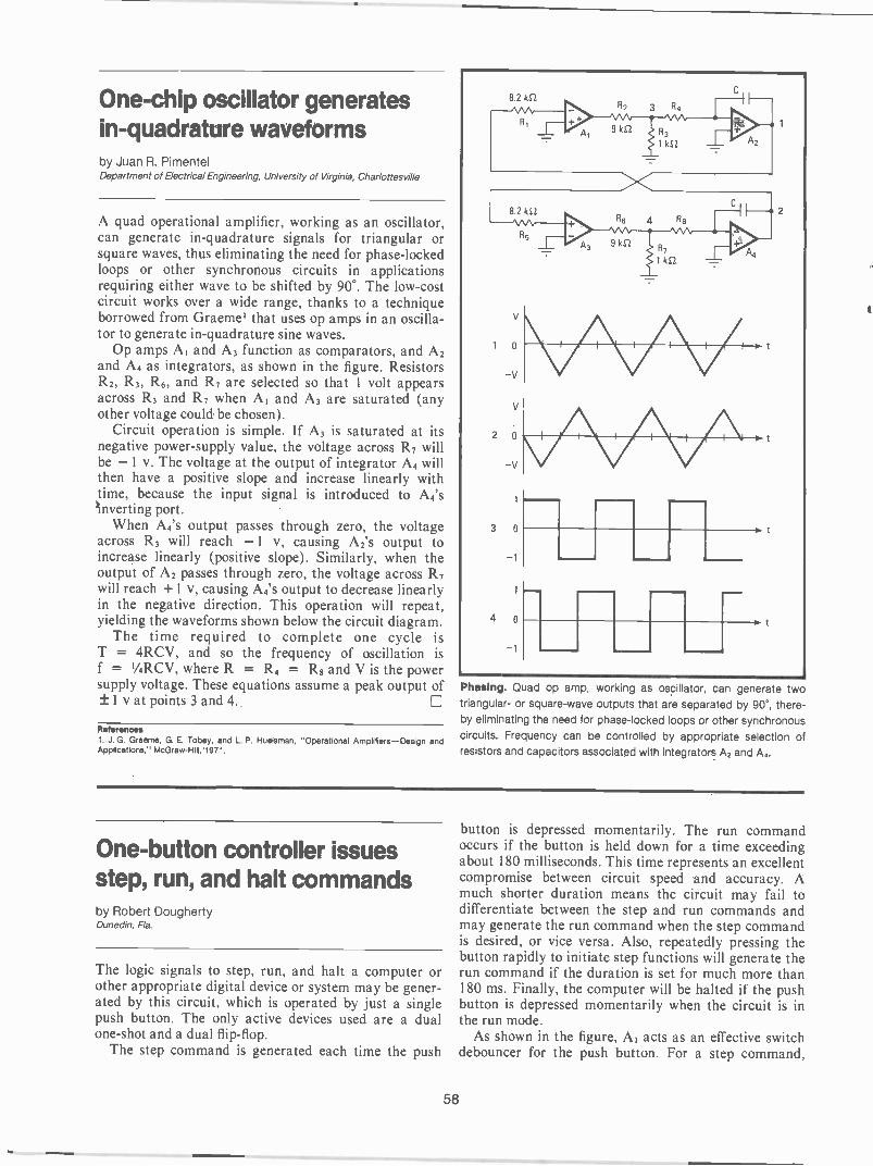
One -chip oscillator generatesin-quadrature waveformsby Juan R. PimentelDepartment of Electrical Engineering, University of Virginia, Charlottesville
A quad operational amplifier, working as an oscillator,can generate in-quadrature signals for triangular orsquare waves, thus eliminating the need for phase -lockedloops or other synchronous circuits in applicationsrequiring either wave to be shifted by 90°. The low-costcircuit works over a wide range, thanks to a techniqueborrowed from Graeme' that uses op amps in an oscilla-tor to generate in-quadrature sine waves.
Op amps AI and A3 function as comparators, and A2and A4 as integrators, as shown in the figure. ResistorsR2, R3, R6, and R7 are selected so that 1 volt appearsacross R3 and R7 when A1 and A3 are saturated (anyother voltage could be chosen).
Circuit operation is simple. If A3 is saturated at itsnegative power -supply value, the voltage across R7 willbe - I v. The voltage at the output of integrator A4 willthen have a positive slope and increase linearly withtime, because the input signal is introduced to A4'slinverting port.
When Aa's output passes through zero, the voltageacross R3 will reach - 1 v, causing Az's output toincrease linearly (positive slope). Similarly, when theoutput of A2 passes through zero, the voltage across R7will reach + 1 v, causing A4's output to decrease linearlyin the negative direction. This operation will repeat,yielding the waveforms shown below the circuit diagram.
The time required to complete one cycle isT = 4RCV, and so the frequency of oscillation isf = 1/4RCV, where R = R4 = R8 and V is the powersupply voltage. These equations assume a peak output of± 1 vat points 3 and 4.
Rirunona1. J. G. Graeme, G. E. Tobey, and L. P. Huelsman, "Operational Amplifiers-Design andApplications," McGraw-Hill, 1971.
Phasing.triangular- or square -wave outputs that are separated by 90°, there-by eliminating the need for phase -locked loops or other synchronous
circuits. Frequency can be controlled by appropriate selection ofresistors and capacitors associated with integrators A2 and A,.
Quad op amp, working as oscillator, can generate two
One -button controller issuesstep, run, and halt commandsby Robert DoughertyDunedin, Fla.
The logic signals to step, run, and halt a computer orother appropriate digital device or system may be gener-ated by this circuit, which is operated by just a singlepush button. The only active devices used are a dualone-shot and a dual flip-flop.
The step command is generated each time the push
button is depressed momentarily. The run commandoccurs if the button is held down for a time exceedingabout 180 milliseconds. This time represents an excellentcompromise between circuit speed and accuracy. Amuch shorter duration means the circuit may fail todifferentiate between the step and run commands andmay generate the run command when the step commandis desired, or vice versa. Also, repeatedly pressing thebutton rapidly to initiate step functions will generate therun command if the duration is set for much more than180 ms. Finally, the computer will be halted if the pushbutton is depressed momentarily when the circuit is inthe run mode.
As shown in the figure, A, acts as an effective switchdebouncer for the push button. For a step command,
58
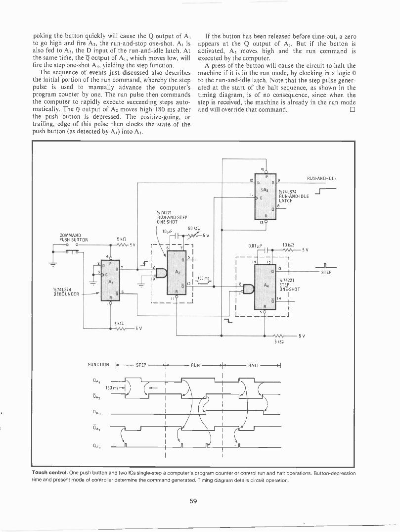
poking the button quickly will cause the Q output of Alto go high and fire Az, the run -and -stop one-shot. Al isalso fed to A3, the D input of the run -and -idle latch. Atthe same time, the Q output of AI, which moves low, willfire the step one-shot A4. yielding the step function.
The sequence of events just discussed also describesthe initial portion of the run command, whereby the steppulse is used to manually advance the computer'sprogram counter by one. The run pulse then commandsthe computer to rapidly execute succeeding steps auto-matically. The Q output of A2 moves high 180 ms afterthe push button is depressed. The positive -going, ortrailing, edge of this pulse then clocks the state of thepush button (as detected by AI) into A3.
If the button has been released before time-out, a zeroappears at the Q output of A3. But if the button isactivated, A3 moves high and the run command isexecuted by the computer.
A press of the button will cause the circuit to halt themachine if it is in the run mode, by clocking in a logic 0to the run -and -idle latch. Note that the step pulse gener-ated at the start of the halt sequence, as shown in thetiming diagram, is of no consequence, since when thestep is received, the machine is already in the run modeand will override that command. El
COMMANDPUSH BUTTON
0
'/ 74LS74DEBOUNCER
5 kft11P--M/o- 5 V
a
Al
10
12
II 0
± 19
10
-7. I
V274221RUN -AND -STEPONE-SHOT
51210µLI0 k
11 _J
5V
180 ms
A31/2 74LS74RUN -AND -IDLELATCH
RUN -AND -IDLE
Q_
Is
13
0.0111F 101(11
HD-NA.A.,- 5 V
5
3
2 4.4m,,t
5k12-'\AAr-- 5 V
FUNCTION STEP
74221A4 STEP
ONE-SHOT
- 14
A
---39
RUN
_J
-5V5k12
HALT
STEP
Touch control. One push button and two ICs single-step a computer's program counter or control run and halt operations. Button -depressiontime and present mode of controller determine the command generated. Timing diagram details circuit operation.
59
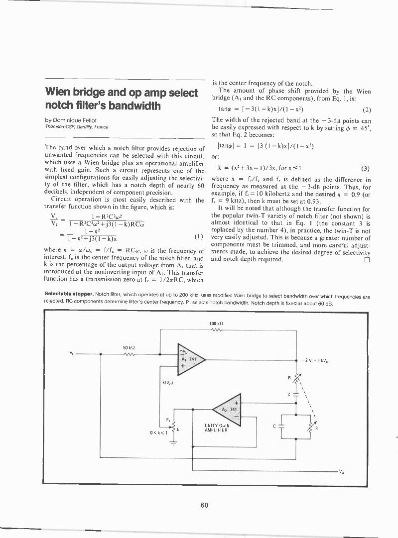
Wien bridge and op amp selectnotch filter's bandwidthby Dominique FellotThomson-CSF, GentiIly, France
The band over which a notch filter provides rejection ofunwanted frequencies can be selected with this circuit,which uses a Wien bridge plus an operational amplifierwith fixed gain. Such a circuit represents one of thesimplest configurations for easily adjusting the selectivi-ty of the filter, which has a notch depth of nearly 60decibels, independent of component precision.
Circuit operation is most easily described with thetransfer function shown in the figure, which is:
V. 1 - R2C2w2V, = 1 -R2C2co2+j3(1-k)RQ..)
1 -x2- 1 -x2 -I -j3(1 -k)x
where x = 0)/co, = f/f0 = RCw, w is the frequency ofinterest, fc is the center frequency of the notch filter, andk is the percentage of the output voltage from AI that isintroduced at the noninverting input of A2. This transferfunction has a transmission zero at f0 = 1 /2rRC, which
(1)
is the center frequency of the notch.The amount of phase shift provided by the Wien
bridge (A1 and the RC components), from Eq. 1, is:
tan4 = [ - 3(1 -k)x]/(1 - x2) (2)
The width of the rejected band at the -3 -dB points canbe easily expressed with respect to k by setting 4) = 45°,so that Eq. 2 becomes:
'tar* = 1 = [3 (1 -k)x]/(1 -x2)or:
k = (x2+ 3x- 1)/3x, for x<1 (3)
where x = fr/f, and fr is defined as the difference infrequency as measured at the -3 -dB points. Thus, forexample, if 1'0=10 kilohertz and the desired x = 0.9 (orfr = 9 kHz), then k must be set at 0.93.
It will be noted that although the transfer function forthe popular twin -T variety of notch filter (not shown) isalmost identical to that in Eq. 1 (the constant 3 isreplaced by the number 4), in practice, the twin -T is notvery easily adjusted. This is because a greater number ofcomponents must be trimmed, and more careful adjust-ments made, to achieve the desired degree of selectivityand notch depth required.
Selectable stopper. Notch filter, which operates at up to 200 kHz, uses modified Wien bridge to select bandwidth over which frequencies arerejected. RC components determine filter's center frequency. P, selects notch bandwidth. Notch depth is fixed at about 60 dB.
60

One -chip comparator circuitgenerates pulsed outputby Virgil Tiponut and Daniel StoiciuTimisoara, Romania
Generating a steady stream of pulses rather than theusual logic 0 or logic 1 output when triggered, thisspecial comparator circuit is useful in many controlapplications. The one -chip circuit is perhaps the simplestway to build what is essentially a low-cost switchedoscillator.
A 711 dual comparator serves as a Schmitt triggerand rectangular -wave generator, as shown in thefigure. The Schmitt trigger (A1, RI, and R2) hasswitched levels Vh and VI, given by:
V' RI + R2 VH
V' - RI + R2 VL
where VH and VL are the high and low output voltages,
respectively (at pin 10), VH = V, - 0.75, and V, is thecomparator's strobe voltage.
The outputs of each comparator are connected in thewired-oR configuration. When the control voltage, V isgreater than the user -set reference, Vref, the output of A2is low. Thus the output voltage, V0, is determined by thesignals at the input to comparator Al.
Al will then begin to oscillate. The output V. willmove high to VH because of the small differential voltagethat exists across the input of AI, charging C through Di
and R3. When the voltage across C, Vf, approaches VH,Al switches, bringing V. low. C then discharges throughD2 and R4 until the voltage across C drops below that atthe noninverting input. V. then moves high again, charg-ing C, and the process repeats.
Circuit operation may be visualized with the aid of thewaveforms shown. Al's switching times, T1 and T2, aregiven by:
T, = C1R3 ln [(VI- VH)/(VI, Vii)]T2 = C1R4 ln [(Vh- VL)/(V1- VI)]
neglecting the output resistance of the comparator.Oscillation ceases when V, is less than V,-. V. then
moves high permanently, since Al is prevented fromaffecting the output state. 111
Pulsating comparator. One 711, wired as Schmitt trigger and oscillator, generates continuous train of rectangular waves when fired bycontrol voltage, V,. Output voltage V. otherwise assumes logic 1 (high) state (when V, < V,e,). Waveforms detail circuit operation.
61

Removing the constraintsof C-MOS bilateral switchesby W. Chomik and A. J. CousinDepartment of Electrical Engineering, University ol Toronto, Canada
Two major limitations imposed on the popular comple-mentary -metal -oxide -semiconductor 4016 switch maybe overcome with this circuit. As well as allowing thesignal magnitude to exceed the power -supply voltage, itenables unipolar control signals to switch bipolar inputsignals. Only a second switch and an inverter need beadded to a standard circuit to remove these operatingconstraints on the signal -handling gate.
Usually, the signal voltage to be passed through asingle switch must be limited to between VDD + 0.7 voltand Vss - 0.7 v, where VDD is the positive supply (drain)voltage and Vss is the minus supply (source) voltage.Otherwise, the signal voltage will cause the forwardbiasing of the diode between the substrate and channelof one mos field-effect transistor, and the gate may bedestroyed.
This problem might arise if the power -supply valueapplied to some active element in a circuit happened tolie outside the voltage range that could be applied to theswitch (VDD - Vss), dictating that the gate must beprotected from input and control signals that saturate tothe supply level.
Furthermore, many circuits, especially those contain-ing operational amplifiers, use bipolar supplies. Theresulting signals to be processed are likely to be bipolar
as well. Yet the channel -voltage constraints inherent inthe design of the 4016 (that is, the fact that the logic 0control voltage, Vss, must be at or below the mostnegative signal voltage, and the logic 1 control voltage,VDD, must be at or above the most positive signalvoltage) means that bipolar supplies and control signalsmust also be applied to the switch if these bipolar signalsare to be passed. Unfortunately, too, many systems usedigital control signals that are unipolar, and so logic -level shifters are needed also, to make this signalsymmetrical with respect to ground.
With the addition of a second bilateral switch and aninverter to a standard op -amp circuit, as shown, thesignal -handling switch can operate from a single powersupply and be driven by unipolar logic at the controlinput in order to pass bipolar signals. Moreover, thesignal can lie outside the VDD- Vss limit of the switches.
The channel voltage of both switches is set by fixingtheir drain potentials at the virtual ground of the op ampor to circuit ground, depending on which switch is on.Because the virtual ground never strays from trueground by more than a few millivolts, the switches willbe protected from burn out, as their channel -voltagelimit will never be exceeded.
When switch A is on and switch B is off, node n willbe essentially at ground potential. When B is on and A isoff, the signal is removed from the op amp's input, butnode n will still be at ground (through B), and the samechannel -voltage conditions will prevail.
Note that the actual input voltage to the gate at noden will never drop more than a few millivolts below the
if the input signal isnegative. Thus, the gate's channel -voltage constraint isalways met. 0
No limitations. Inverter and gate B enable switching of bipolar input signals by unipolar control signals at gate A and also allow magnitude ofinput to exceed gate's supply voltage. Node n is held near to ground at all times, so that channel -voltage limit of gate is never exceeded.
Magnitude of signal at node n never exceeds control -signal potential, enabling gate to switch properly.
10k52 n
INPUT SIGNAL
VDU (+)
V. = 0
' 4009
1.4016
CONTROLSIGNAL
VDD ON
0 OFF
10 kS2
VDD (+)
741
(
OUT
62

Diodes adapt V -f converterfor processing bipolar signalsby Jerald GraemeBurr -Brown Research Corp., Tucson, Ariz
Two diodes and one operational amplifier will enable avoltage -to -frequency converter to process bipolar inputsignals, thus adapting it for operation in absolute-valuecircuits. Using the integrator of the converter eliminatesat least one of the op amps normally required for suchabsolute -value converters. Moreover, the approach issimpler overall than ones that bias the converter's inputsat a value midway between supply voltage and ground.
When input signal e, is positive (see figure), diode D,becomes forward -biased and D2 is reverse -biased. Opamp AI, which isolates the signal from the offset andbias currents of the V -f converter, then acts as a nonin-verting amplifier with a gain of 1 + R2/RI; it creates anintegrator feedback current equal to it = 10e,/R3,provided that R4 = (RI+ R2 + R3)R3/(Ri+ R2- R3).The voltage e,(1 + R2/R1) at the inverting input of theV -f converter is then transformed into a correspondingfrequency.
For negative values of e DI is back -biased and D2 is
forward -biased, enabling the op amp's output signal tobe applied to the noninverting input of the V -fconverter.In this configuration, the gain is negative, so that theintegrator current generated has the same polarity asbefore. Thus the V -f converter cannot distinguish posi-tive and negative voltages having the same magnitude,and so generates the same frequency for both signals.
If DI and D2 are replaced with the emitter -base junc-tions of any general-purpose transistors and the transis-tors' collectors are used to drive lamps or other indica-tors, the polarity of the input signal can be displayed.Care should be taken to avoid reverse emitter -basebreakdown caused by large input -signal levels by placingdiodes in series with the base of each transistor.
The accuracy of the converter is determined by thesame factors as affect conventional absolute -valuecircuits: resistor -ratio matching and the op amp's inputoffset voltage.' It is most important that the RI-R.,resistor values be correct for a given gain, as they have apart in equalizing circuit gain for both signal polarities.
The op amp offset voltage must also be minimized.The standard trimming procedure will in effect removeany offset at the point where the diodes switch. Theoffset at the output of the V -f converter can then beremoved by trimming its integrator circuit.
Iteferencos1. J. Graeme, "Applications of Operational Amplifiers-Third Generation Techniques,"McGraw-Hill, 1973.
R2
'VSA,100 kS2
+15 V
BB 351013
el 0
15 V
184154
R3
40.2 kS2kS2
0.01p F
84
11 --
INTEGRATOR CURRENT
+15 V
86.6 kS2
07
1N4154 4.7 kS2
A-,
BB VFC 32
-15 V
Absolute switchover. D, and D2 switch on alternately as polarity of input signal changes, thus maintaining direction of integrator current. V -fconverter cannot distinguish between signal polarities of the same magnitude and so generates the same frequency for both.
63

Prescaler and LSI chipform 135 -MHz counterby Gary McClellanLa Habra, Calif.
Combining a prescaler designed for very high frequen-cies with large-scale integrated circuits and a few otherdevices builds a multifunction frequency counter capableof working at 135 megahertz. The counter, which usescomplementary -metal -oxide -semiconductor and emitter -coupled -logic chips, has many desirable qualities, includ-ing the ability to measure the period of a waveform,moderate power consumption (100 milliamperes, includ-ing displays), good sensitivity (16 millivolts at 135 MHz),and portability.
In the frequency mode (selected by switch SI), signalsat the input are limited by the resistance -capacitancenetwork and two diodes (see figure) so as to preventoverloading of AI, the National DS -8629N prescaler. AI
amplifies the signal and divides it by 100, and then it iscounted by A2, the Intersil ICL-7216B.
The ICL-7216B contains a counter, a display multi-plexer, a seven -segment decoder, and digit and segmentcircuits for driving A3, the HP 5082-7441 display. Thechip also provides timing for the system, including thenecessary oscillator circuitry and frequency dividers togenerate the gate, latch, and reset pulses for multiplex-ing the display and controlling the sampling interval(selected by S2).
In the period mode, input signals are limited in orderto protect Q1, an impedance converter. A simple preampand Schmitt trigger, A3, converts the signal to appro-priate levels for A2.
The counter also has provision for an external oscilla-tor input. When properly used with an external 10 -MHzstandard, it makes measurements with a high degree ofaccuracy. S3 enables the measurement.
Calibration is easy. A signal of known frequency isconnected to the frequency input (a 100 -MHz signal isideal), and the 15-picofarad capacitor, which is in paral-lel with crystal Y I, is adjusted for a matching counter
, reading. Accuracy is not greatly affected by the supply
5V18
EXTERNALOSCILLATORIN
FREQUENCYIN
Ri
C6
11
C6
22 pF 15 PF2
39 pF Y1 R3
10 MHz T 22 MEt25
24
0.01µF =C2
1N4148 C1
A7
C5
10.1µF05 w
- 1N4148
47MO,
I2
C10 I+47µF1
C9
0.5pF R4
PERIOD1 kL2
IN
D3
1N4148
04
0.001 pFDS 8629N
S3
R
10 kL2
C361 1 D4
o.oi /IF
- -0.01 p F
Cil
1+TIS-75 2
1001.IF
R6
220 Et
R5
1 ME2
A3
7400
3
117 R8Vos V1r..
680 E2 470 E2
13
8
12
R9
12 kEt
810
10 kS2
27
FREQUENCY
PERIOD oSIa
A2
ICL72168
28
20F111 -R17
17 14B
16 2C
19 10
21 8
15 16
22 12 S
7 x 470 S250827441
DISPLAY
4 150,
6 1302
503
7 9
9 704
DS
10 506
o,3
12
R19
Ye%
10 kt2
S160, FREQUENCY
PERIOD
S2R19
10 k2
0.01 s
c- 0.1 s0- 1.0 s
10.0 s
Counting high. Three -chip circuit uses prescaler and LSI chip in frequency counter capable of operating at 135 MHz. Circuit draws total of100 milliamperes, has good sensitivity, is portable. Counter should be built on double -sided pc board for best performance.
64

voltage, as the counter holds to within two counts of thedisplayed frequency over 4.5 to 5.5 volts.
The counter is best built on a double -sided printed -circuit board. Parts layout is not critical, with the excep-tion of the input leads, which should be positioned away
from the display. Also, AI should have foil running on itsunderside, to act both as a heatsink and as shielding. 111
Clock module supplieschart -recorder time markersby G. J. MillardVolcanological Observatory, Rabaul, Papua, New Guinea
Utilizing the display segments of a standard digital clockmodule-or more precisely, the signals that drivethem-this circuit enables a chart recorder to markintervals of 1 minute or 1 hour or both. Use of an alreadybuilt electronic clock, such as National Semiconductor'spopular MA1012C, guarantees a chronometer that is
accurate, simple to construct, and low in cost ($25).The 1 -minute markers are developed from the signals
that drive segments d and e of the minutes-unit displayin the MA1012C. These signals, which are readily acces-sible, drive two frequency doublers, A1-A4, that in turnproduce a pulse at point C every minute. The pulse thentriggers a one-shot (A5, A6, R1, C1), which switches therelay on for 2 seconds.
If desired, markers can be generated at 1 -hour inter-vals by connecting segments d and e of the hours -unitdisplay to a similar circuit, the output of which isconnected to point D. To differentiate between theminute and hour markers, the relay on -time should beset at 4 seconds by making RI in the correspondingcircuit 680 kilohms. El
I I MINUTES -UNITSEGMENT
I FROM MA1012C
27 k12
12 V
56 kS1 56k12
0.01r
-1I
Al 0.01 pF
27 kSZ
1N914
FREQUENCYDOUBLERS
0.01 pF
EP0.01 pF
56 kn 56 kS1
12 V
011N914
D C,
12 V
330 kS2
10 pF
MONOSTABLE
A622 kSZ
1N914
TO SIMILAR 22 1(12
HOURS -UNIT -We--CIRCUIT
12V
2N3642
A1, A3, A6: 74C04
A2, A,: 74C00
A5: 74CO2
MINUTES 0 1 2 3 4 5 6 7 8
SEGMENT °
A
SEGMENT E
B
C
RELAYITO PEN ANDAPPROPRIATECIRCUITS INCHARTRECORDER)
On time. Markers at 1 minute and 1 hour are derived from signals that drive segments d and e of minutes -unit and hours -unit display,respectively, in MA 10 12C clock module. Relay's on -time is controlled by RIC,. Timing diagram details operation for minute markers.
65

Filter levels output swingof Wien -bridge oscillatorsby Maxwell G. StrangeGoddard Space Right Center, Greenbelt, Md.
Although the output of a tunable Wien -bridge oscillatornormally exhibits a large change in amplitude as afunction of frequency, a standard active filter will hold itto within ± 0.2 decibel over a ± 20% frequency range. Inthis application, the filter's response is set to compensatefor the amplitude variation of the oscillator. Most alter-native amplitude -stabilization circuits tend to draw highpower, create appreciable sine -wave distortion, or stabi-lize slowly.
The technique can be easily implemented at anyfrequency over the operating range of the oscillator,since the filter's component values are easy to calculate,being inversely proportional to frequency. The circuitshown was designed to control the speed of a 60 -hertz
Stability. Active filter's roll -off characteristics compensate for oscil-lator's inherent amplitude change with tuning, keeping output levelwithin ±0.2 dB in range of interest. Sine -wave distortion is alsodramatically reduced-from 1% at oscillator output to 0.1%.
22 kn 100 1(1-2
20 kn(OUTPUTAMPLITUDE)
1
0.022µF
-15 VOSCILLATOR
180 kn 100 kS2 DUAL 180 Id2
15 kS2
R
0.0222(F
15 Ica
0.222(F
0.22µF
I I
1 % (FREQUENCY) 1%
1N4148 = =1N4148 43 kf2
100 ksz
(a)
+15 V
INJ OUTPUT
48.* 74 Hz10 V PEAK TOPEAK
56 ks-2.
ALL CAPACITORS: 50 V POLYCARBONATE
66
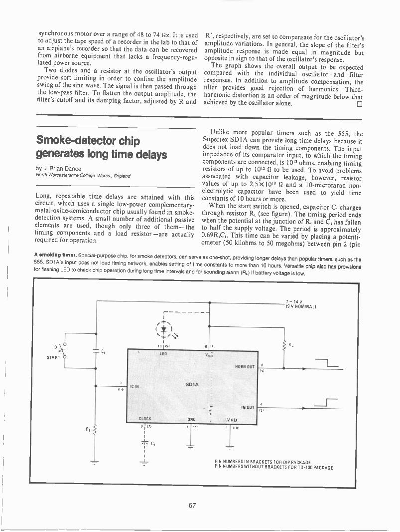
synchronous motor over a range of 48 to 74 Hz. It is usedto adjust the tape speed of a recorder in the lab to that ofan airplane's recorder so that the data can be recoveredfrom airborne equipment that lacks a frequency -regu-lated power source.
Two diodes and a resistor at the oscillator's outputprovide soft limiting in order to confine the amplitudeswing of the sine wave. The signal is then passed throughthe low-pass filter. To flatten the output amplitude, thefilter's cutoff and its damping factor, adjusted by R and
R', respectively, are set to compensate for the oscillator'samplitude variations. In general, the slope of the filter'samplitude response is made equal in magnitude butopposite in sign to that of the oscillator's response.
The graph shows the overall output to be expectedcompared with the individual oscillator and filterresponses. In addition to amplitude compensation, thefilter provides good rejection of harmonics. Third -harmonic distortion is an order of magnitude below thatachieved by the oscillator alone. El
Smoke -detector chipgenerates long time delaysby J. Brian DanceNorth Worcestershire College. Worcs., England
Long, repeatable time delays are attained with thiscircuit, which uses a single low-power complementary -metal -oxide -semiconductor chip usually found in smoke -detection systems. A small number of additional passiveelements are used, though only three of them-thetiming components and a load resistor-are actuallyrequired for operatiol.
,A1
Unlike more popular timers such as the 555, theSupertex SD1A can provide long time delays because itdoes not load down the timing components. The inputimpedance of its comparator input, to which the timingcomponents are connected, is 1013 ohms, enabling timingresistors of up to 1012 12 to be used. To avoid problemsassociated with capacitor leakage, however, resistorvalues of up to 2.5 X 10¹⁰ SI and a 10-microfarad non -electrolytic capacitor have been used to yield timeconstants of 10 hours or more.
When the start switch is opened, capacitor C, chargesthrough resistor It, (see figure). The timing period endswhen the potential at the junction of R, and C, has fallento half the supply voltage. The period is approximately0.69R,C,. This time can be varied by placing a potenti-ometer (50 kilohms to 50 megohms) between pin 2 (pin
A smoking timer. Special-purpose chip, for smoke detectors, can serve as one-shot, providing longer delays than popular timers, such as the555. SD1A's input does not load timing network, enables setting of time constants to more than 10 hours. Versatile chip also has provisionsfor flashing LED to check chip operation during long time intervals and for sounding alarm (RL) if battery voltage is low.
START
141IC IN
I-
LEO
SD1A
CLOCK GNO
8 171 7 161
1
C1
5 131
VDO
HORN OUT 6
IN/OUT
LV REF
141
4
7 - 14 V(9 V NOMINAL)
PIN NUMBERS IN BRACKETS FOR DIP PACKAGEPIN NUMBERS WITHOUT BRACKETS FOR TO -100 PACKAGE
67

12 of the dual in -line package) and the supply.At the end of the timing period, the voltage at the
input/output port rises to VDD - 0.5 volts. The hornoutput falls to near zero, serving as a current sink for theload, RL, which may be an alarm or just a resistor. Thehorn output can sink at least 300 milliamperes.
A light -emitting diode connected to the appropriateport of this versatile chip can be made to flash every 40seconds during the timed period if a 10-microfaradcapacitor is connected to the clock pin. The flashingprovides a useful indication that the circuit is operatingduring long timing periods. The frequency of the flash-ing is controlled by the value of CI or can be adjusted by
connecting a potentiometer between the clock pin andVDD for decreasing the period or between the'clock pinand ground for increasing the period.
The SD1A also includes a circuit for sounding thealarm every 40 seconds if the supply voltage is low(below 7 v). Here the low -voltage reference pin, LV REF,has been grounded so as to disable this feature.
The cost for the SD1A is $2.50 in the TO -100 packageversion, and $2 in the DIP. The manufacturer does notyet have authorized distributors for the device, however,and thus at this time the SD1A can only be purchased inlots of 50 or more directly from Supertex, 1225 BordeauDr., Sunnyvale, Calif. 94086. f=1
Opto-isolated detectorprotects thyristorsby Charles RoudeskiOhio University, Athens, Ohio
Although gating a thyristor with short pulses greatlyreduces the gate and driver dissipation, failure of thedriving logic can turn on the thyristor full time, possiblydestroying it, the driver, and their supply. Described hereis an opto-isolated zero -crossing detector that generatesa 100 -microsecond pulse each time its 60 -hertz power -line input traverses through zero. Besides isolating forthe logic element, the circuit terminates the generationof pulses if almost any detector component fails.
Most of the line voltage (see figure) is dropped acrossthe 10-kilohm input resistor before it is rectified. The25-microfarad capacitor charges during most of the60 -Hz cycle, but the 2N2907 transistor is held off by anyfull -wave rectified voltage above 2.3 v.
As the line voltage drops to about 4.5 v, the transistorbegins to turn on and the capacitor discharges throughthe 41'126's photodiode, sourcing about 14 milliamperes.This produces a pulse centered about the zero crossing.Wider pulse widths are obtained by reducing the value ofthe 15 -kg resistor. If a longer rise time is tolerable, the33-k0 resistor in the base lead of the optocoupler'sphototransistor can be eliminated.
The 3-v zener establishes the reference voltage for thecircuit. El
Protction. Zero -crossing detector uses optocoupler for gating of thyristors by power line. Output pulses, produced 120 times per second asinput voltage traverses through zero, last 100 As. Output of 4N26's phototransistor will be zero if most any element in detector fails, therebyprotecting thyristor, driver, and supply from damage that would be caused by activating the thyristor continuously.
120 Vac
1N914
10 kS2
VARO RECTIFIERBRIDGE (DUALIN -LINE PACKAGE)
33
0 kL.!
25pF
68

Industrial counter handleswidely varying intervalsby Rudolf E. SixThe Detroit News, Electronics Department, Detroit, Mich.
The time intervals between consecutive events in indus-trial processes can often vary over several decades, creat-ing a problem if their values are to be stored in amicroprocessor -based system. Normally, a great manyinput/output ports would be needed to handle, say, the24 significant bits needed to represent a 10 -second inter-val measured with a 1 -megahertz clock. But this counterrequires only 10 output lines to represent intervals rang-ing from 1 microsecond to 10 seconds, making it easy fora 16 -bit data system to process a 24 -bit binary number.
Wiring a set of 4 -bit counters, A1-A7, as a one -decadedivider is what makes it possible for fewer lines to beused. At the start of a measurement, a string of 74160counters immediately begin to divide down a gated1 -MHz clock signal into seven decades of time rangingfrom 1 microsecond to 10 seconds in duration, as shown.The outputs of Al-A, are then presented to Ag, the74152 eight -to -one multiplexer.
A10 and A11, two 74161 binary counters, are incre-mented once each microsecond until their combinedcount reaches 99. G1 moves low at this time. On count100, G1 moves high and presets A10 A11 to a count of 10,and steps the multiplier counter A9. A9 enables AB toadvance to the next decade position (D, to D,+1). A10-A11now counts at one tenth of the rate it did before A8 wasstepped to DH.1.
The process continues until such time that themeasurement interval is terminated. On the seven bina-ry -count lines will be a binary -equivalent number that is
4 5V001 ps
1 -MHz Al15 D1
GATEDCLOCK
74160 10 /Is9 6 5 4 3 9 6 4 5 3 1
6 7404
2
A8
74152
02100µs
9
A9
74161
Al
74161
7, 10Al
741617,10,
15
27,10
2 A2
7416012 3 14 12 13 14 II 12 13 14
B10
15 032 A3
1 74160 1 ms
1/6 7404
7,10 9
2 A4 15 15 04 5VI 74160 10 ms
2 3
10
4 5 6 11 12
7,10
2A5 15 D5 G
1 74160 100 niS 74H30
7,10
2 A6 15 13 06741M 1s
12 07
10 9
MSB
8
LSB
7 6LSB
5 4 3 2 1
MSB7,10.
152 A7
MULTIPLIER BINARY COUNTCLEAR 74160 10s
1/6 7404
Line reduction. Counter that measures time interval between two events over a range of 1 microsecond to 10 seconds needs only 10 outputlines to display the results and store them in a microprocessor -based system. System resolution is adequate for most applications but may beincreased if an extra 74161 is cascaded with the it1/4,0A, counter, at a cost of three more output lines.
69

related to the number of pulses in the gated clock signal.The actual (decimal -point) magnitude in microseconds,milliseconds, etc., is determined by the remaining threemultiplier output lines, which indicate the decade value(130---D7) as a three -bit binary number.
For example, an output of 01010001 on the binarylines combined with an output of 001 on the multiplierlines indicates a time interval of 810 ;is between two
events. After the computer has stored the information, aclear signal resets all the counters.
The resolution of the system (1 i,,ts at the low edge, 10 sat the high end) is adequate for most applications, but itmay be improved if an additional 74161 counter iscascaded to the A10-A1 1 circuit. This extension willincrease system accuracy by 1 bit, but then three addi-tional output lines will be required.
Three LEDs display responseof null -detector circuitby William A. PalmMagnetic Peripherals Inc., Minneapolis, Minn.
Three light -emitting diodes provide a visual readout forthis null-detector/bridge circuit that can be used tomatch resistors to within 0.5%. The LED display is bettersuited for production -line measurement purposes than anoutput meter, is lower in cost, and takes up less space.
Circuit operation is straightforward. Transistors Q1and Q2 will both be on when bridge resistor Rx, theresistor to be tested, is approximately equal to Rrcr, thereference resistance, because the differential voltage atthe input ports of the 741 operation amplifier is near
zero. Thus the output of the 741 assumes its midrangevalue of 4.5 volts, and LED A turns on. At this time, thevoltage dropped across A and the 100 -ohm collectorresistors connected to Q1 and Q2 ensure that D1 and D2cannot conduct, and so B and C cannot light.
When the differential voltage at the inputs of the opamp increases or decreases because of a change in R,one transistor will turn off, and this action will divert allcurrent through LED B or C instead, depending on thepolarity of the input voltage.
The null -detector response is illustrated within thecircuit diagram. Note that there is no single step -transition from one region to another, but rather twosmall regions where two LEDS may be on simultaneously.These regions correspond to a value of R that is about0.5% to either side of Rf.
5 kS2
9 V
RREF
BALANCE
470 S2
GAIN
5 kS23
Rx
741
4
250 1(12
Rx = RREF RX RREF RX = RREF
CD @NULLDETECTOR RESPONSE
1.8 kS2
1.8 kS2
100 12
470 12
01
2N4258
100 S2
ABOVE RREF
CENTER
B
022N3646
BELOW RREF
5V -I;Es Gl
5V' 02
Light reaction. Null detector uses simple LED readout to indicate if test resistor R. is below, equal to, or greater than test resistance Re, IfR. = Ref, 741 output sits at midpoint value of 4.5 volts and LED A lights. Otherwise, output of 741 turns off one transistor, diverts current from
other transistor through B or C, depending on polarity of input voltage difference. Null -detector response is illustrated.
70

Biaxial modulators doubledata -system transfer rateby Robert J. StetsonStorage Technology Corp., Aurora, Ill.
The information -handling capacity of simple datasystems will be doubled if a scheme employing bothpulse -width and pulse -amplitude modulation is used tomultiplex data through the transmission line. Morespecifically, a one -cable, single -channel system can beexpanded to two channels, enabling data to be sent attwice the original bit rate. Such a biaxial modulationcircuit is far more economical than those using separatecables and transmitter -receivers for each channel and is
less complex and costly on a per -channel basis than thoseusing synchronous eight -channel digital multiplexers.The biaxial transmitter and receiver are simple to build.
Figure la shows a transmitter suitable for transferringdata through a line at 4,800 bauds per channel, or 9,600bits of data per second for two channels. The X- and Y -input data, which are non -return -to-zero (NRz) pulsetrains, operate at the same baud rate and are synchro-nized with the bit clock. The latter is framed at themidpoint of the data, as shown in the timing diagram(Fig. 1 b).
The width of the pulse emanating from transistor Q1and therefore from the output line is a function of the X -input data. Q1 normally conducts with no input signal.Generally, the bit clock periodically fires A1, a one-shotwith an on time of 200 nanoseconds, and thus a 5 -volt,200-ns pulse appears at Q1 if X and Y are at logic 0.
When the X data is high, however, a bit clock pulse
DATA2
5V
50 162
__,._ 20 pF141
(a)
SPACE200 ns MARK Ell] V
SPACE= 5 V
Y DATA
X DATA
BIT CLOCK1 1
10V
LINE 5 V
0 V --(b)
1 1 1 1
_n_ ILL
1 1 1 1 1 1 1 1 1
_Lilt 11. Modulation multiplexing. Two -mode modulation permits low-cost data multiplexing. Pulse -width modulation of X data combined withpulse -amplitude modulation of Y data doubles the capacity of one -cable systems (a). Timing diagram (b) details modulation processes.
71

sends A2 high for a period of 800 ns, overriding A1. Theresult is that the output of Q1 is a pulse -width -modulatedwaveform having a width of 800 ns at 5 v for a logic 1input at the X port and a pulse 200 ns wide at 5 v for alogic 0 at the X port.
The output of Q2 and the line, on the other hand, ispulse -amplitude -modulated by data on the Y port. Whenthe Y input is high, and X = 0, the output of the signalline will be 10 v for a period of 200 ns after the arrival ofthe bit clock signal. If both X and Y are high, the lineoutput will be at 10 v for 800 ns. The four possible X -Yinput combinations are summarized in the timingdiagram. The PWM-PAM signal that is to be sent over
cable to the receiver appears at the line output, as shown.The line signal is first introduced to the receiver end of
the system through two LH0042 precision comparators(Fig. 2a). The 10-kilohm resistors limit the input currentto well below the comparators' rated maximum of 200microamperes. The Y comparator clips the signal, sothat only the 5 -to -10-v portion is seen at test point 1
(TP1). Note that the Y data is demodulated but not yetin the form it was originally at the transmitter, that is,reconstructed. The diode bridge at the input of the 7413sserves as a combination limiter and zero -crossovernetwork to aid in signal recovery. The output of one7413 fires the 74123 one-shot, A3, producing the V
5V20 kS2
LINE
LH0042
10 kS2
20 kS2
TP1 0
5V
Y27413
'h 7474
YD
1 kS2
2
5V
110
8 pF15 114
12
13 A3
%274123
A`I CLOCK
(a)
5V
30 kS2
1 Kt
7 1620 pF
10B A4
/274123
A12
2
X CLOCK
30 kS25V
10 k11
15
B A5
Y274123
A
20 pF14
4
'/27474
C 0
pF7T10 12
/2741239 A
XD
BIT CLOCK
LINE 5V
0 V
TP1
Y CLO
YD
XD
IM111 .1111=1M111 ILL__1111. JL
CK11111111111IIIII
BIT CLOCK
Ib)I I I 1 1 H I I 1 I I
(c)
LINE
10 V
5V
0V
TP1(HIGH-LEVELADJUSTMENT)
TP2(LIMITERADJUSTMENT)
1TV
NO PULSES IN THESEINTERVALS
SET R22 FOR EQUALMAXIMUM AMPLITUDE
2. Rocovery. Demodulation process is largely inverse to operation performed at transmitter. X and Y comparatorsseparate pulse -width- and
pulse -amplitude -modulated signals, generate XD and YD with aid of several one -shots and flip-flops (a). Timing diagram (b) aids in
understanding the circuit's reconstruction operation. Two circuit adjustments optimize receiver performance (c).
72

CLOCK signal to regenerate the Y data (YD).The PWM portion of the receiver derives its signal from
the X -data input component. The line signal is applied tothe D input of the 7474 to generate the XD signal. The7474 is also clocked by the same input signal through the74123 one-shot, A4, on the positive edge of each outputpulse of the x CLOCK.
The positive -going edge of the X CLOCK signal occurs400 to 600 ns after A4 fires. If the line -input signal is alogic 0 (200 ns wide), a space will be clocked in at the Dinput of the 7474 storing the XD data. If, on the otherhand, the X input is at a logic 1 (800 ns wide), a markwill be clocked through, since the X pulse will still bepresent on the arrival of the X CLOCK signal. The trailingedge of x CLOCK also fires A5 and A6, two monostablemultivibrators, for 400 to 600 ns. This enables the bitclock signal, which originated at the transmitter, to be
recovered also, as shown in the timing diagram (Fig. 2b).To set up the most efficient circuit, a scope is required.
Also, the X and Y data inputs should be initially tied toground at the transmitter. The scope should then beconnected to the signal line cable and R1 adjusted for apeak amplitude of 5 v. After a logic 1 is applied to the Yinput, the signal line pulses should rise to at least 10 v.
At the receiver end, the scope should be connected toTP1 and R,. adjusted as seen in Fig. 2c. Next, the scopeshould be connected to TP2 and R2a adjusted as shown.A slight shift between the X and Y data output willoccur, basically because of the internal -timing methodused to recover the data. The output data will otherwisebe a replica of the original information transmitted.
Go/no-go tester checksoptocoupler's transfer ratioby S. AshokRensselaer Polytechnic Institute, Troy, N. Y.
This extremely simple circuit performs a go/no-go teston the quality of an optocoupler. Here, an operationalamplifier and a zener diode are used to determine if themost fundamental parameter of the optocoupler, itsforward current -transfer ratio, a (which is the ratio ofthe phototransistor's output current to the photodiodeinput current), is greater or less than a preset value.
The operation of the circuit is based on the principlethat the phototransistor tends to saturate if the currentforced into its collector lead is less than ai, where i is the
Light test. Op amp and zener diode checkoptocoupler quality by determining if its
forward current -transfer ratio, a, is above orbelow preset value. If a is above value set bycurrent sources 1, and 12, phototransistorsaturates and Vb, = 0, indicating goodelement. Otherwise, the zener breaks down,and Von, = 5, indicating bad device.
photodiode current, and that it tends toward avalanchebreakdown if the current is higher than that amount.The forced current is (I, - 12), where I, and 12 arecurrent sources. The preset value of a corresponding tothese currents will thus be (I, -12)/11. Adequate currentsources for 11 and 12 can be implemented by usingvariable resistors returned to + 15- and - 15 -voltsupplies as shown in the figure.
Typically, the phototransistor breakdown voltage isgreater than 5 v, so that if the value of a is lower thanthe preset figure (bad optocoupler), the current into thezener-transistor combination will be greater than a the5-v zener will break down, and V., will then go to 5 v(logic 1). If on the other hand, a is higher than the presetvalue (good optocoupler), the phototransistor will satu-rate and there will be a logic 0 at the output.
Note that the polarity of 12 should be reversed ifoptocouplers with Darlington outputs are tested, becauseDarlington circuits have an a that is greater than unity.
OPTOCOUPLERUNDER TEST
RI
100 kn
-15 V
5V
CA324
R2
100 kn,
+15 V
Volt
73

Low -level -light detectorchecks optical cables fastby Edward W. RummelA. B. Dick Co., Chicago, Ill
A standard phototransistor and a quad operationalamplifier can be used as a total -energy detector ofpulsed -light signals that propagate through fiber-opticcommunications systems. Such a circuit is especiallyuseful for checking and comparing the condition of longfibers when the light intensity at the source is keptconstant. Alternatively, it may detect changes in lightintensity or pulse widths with a given fiber.
Current from the Fairchild FPT130B phototransistordrives AI, a bipolar-field-effect-transistor op amp thatserves as a current -to -voltage converter with anextremely high input impedance (see figure). The photo -transistor has high sensitivity and a low dark current-only 10 nanoamperes flows for zero radiant -input flux. ItJas been given a flat lens to facilitate the addition of
fiber-optic couplers, spectral band-pass filters, and so on.This input configuration enables the circuit to give a
linear response to light levels ranging from 100 to 10,000ergs per square centimeter, provided each pulse in agiven train has a width of no less than 10 microseconds.The phototransistor's low parasitic capacitances contrib-ute to the high response speed of the circuit. The lowinput bias current (0.4 nanoampere) and high slew rate(3.5 volts per microsecond) of Al and subsequent bi-FETamplifiers also contribute to the speed and accuracy. The100-kilohm trimming resistor at the output of Al isprovided to eliminate the variations in sensitivity causedby the 2:1 gain spread of the combination of the photo -
transistor and the optical components.A2 is a standard RC integrator that produces a voltage
directly proportional to the total light energy received.As both Al and A2 operate in the inverting mode and areon the same bi-FET chip, offset voltages appearing at theoutput of AI are virtually canceled by the input offsetvoltage of A2. The cascade connection of AI and A2shown also allows a high degree of freedom in the choiceof source voltages for the circuit.
The low input -bias current of the bi-FET amplifiersmakes it feasible to use low -value, and hence low-cost,
1N914
TRIGGER N ,C'0.001 I./FT
FIBER-OPTIC 12.6 VTRANSMISSIONLINE
BANDPASSFILTER
FPT130B
4.2 V
10
1 22MS2
4.2 V
it
1N914
22 MSZ
4.2 V
SENSITIVITY
2N5953
0.001-µF, 5%
POLYCARBONATE ORPOLYSTYRENE
TL064: TEXAS INSTRUMENTS QUAD BI-FET AMPLIFIER OR EQUIVALENT
12.6 VTR169 -(MERCURY, I I0.1 NF500 mA-H)
THRESHOLD
ANALOG OUTPUTTO BUFFER AND
SCOPE
12.6 V
1 A4
1 M12FILM
12.6 V
500 kS2FILM
4.2 V
DIGITALOUTPUT
Light monitor. Phototransistor and bi-FET op amps form $5 light detector useful for checking optical communications systems. Circuitresponds linearly to light levels in the range of 100 to 10,000 erg/cm2. Circuit runs for 500 hours from a 12.6-V mercury battery.
74
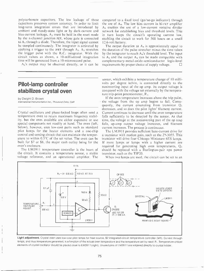
polycarbonate capacitors. The low leakage of thesecapacitors preserves system accuracy. In order to limitlong-term integration errors that are introduced byambient and steady-state light or by dark -current andbias -current leakage, A2 must be held in the reset modeby the n -channel junction FET, whose gate is connectedto A3 through a diode. Therefore, the input signal cannotbe sampled continuously. The integrator is activated byapplying a trigger to the JFET through A3. A3 stretchesthe trigger pulse with the RIC, integrator. With thecircuit values as shown, a 10 -millisecond integrationtime will be generated from a 10 -microsecond pulse.
A2's output may be observed directly, or it can be
compared to a fixed level (go/no-go indicator) throughthe use of A4. The low bias current in bi-FET amplifierA4 enables the use of a low -current resistive dividernetwork for establishing bias and threshold levels. Thisin turn keeps the circuit's operating current low,enabling the circuit to work for 500 hours on a small12.6 -volt battery.
The output duration at A4 is approximately equal tothe duration of the pulse stretcher minus the time takenby the integrator to reach A4's threshold level. The inputto A3 and the output A4 can be made compatible withcomplementary -metal -oxide -semiconductor logic -levelrequirements by proper choice of supply voltage.
Pilot -lamp controllerstabilizes crystal ovenby Dwight D. BrownInternational Instrumentation Inc., Thousand Oaks, Calif
Crystal oscillators and phase -locked loops often need atemperature oven to retain maximum frequency stabil-ity, but the ones available are either expensive or usespecial components not readily at hand. The oven (left,below), however, uses low-cost parts such as standardpilot lamps for the heater elements and a one -chipcontrol and sensing circuit that can maintain the temper-ature to within 0.5'C of the set value. The oven can bebuilt for $7 or $8, the major cash outlay being for theoven's enclosure.
The LM3911 temperature controller is the heart ofthe circuit. It contains a temperature sensor, a stablevoltage reference, and an operational amplifier. The
sensor, which exhibits a temperature change of 10 milli-volts per degree kelvin, is connected directly to thenoninverting input of the op amp. Its output voltage iscompared with the voltage set externally by the tempera-ture trip -point potentiometer, R1.
If the oven temperature increases above the trip point,the voltage from the op amp begins to fall. Conse-quently, the current emanating from transistor Q1decreases, and so does the pilot lights' filameitt current.Current continues to decrease until the oven temperaturefalls sufficiently to be detected by the sensor. At thattime, the voltage at the noninverting port of the op ampfalls, op -amp output voltage increases, and filamentcurrent increases. The process is continuous.
The LM3911 provides sufficient base -current drive fora transistor with modest gain, such as the 2N3055. Thistransistor will drive four Chicago Miniature 6ES lamps.If more lamps or lamps with a higher current arerequired for generating high oven temperatures, (:),should be replaced with a Darlington -pair npn powertransistor, such as the TI P20.
When two lamps are used, the circuit can be set to an
TEMPERATURETRIP -POINTADJUST
0.1 µF
V=15
R2 = (V-6.8) Id -2 2 8.2 Id -2 AT 15 V
f6.8 V
200 kt2
SENSOR
1N914
50 Id?
LM3911
CM 6ES
0,2N3055
USE TIP 120IF i>200 mA
CRYSTAL
SOLDER LEADS5-8 TO CRYSTAL
LM3911
PRINTED CIRCUIT BOARD
Light adjustment. Crystal oven uses low-cost pilot lamps for heat source, $2 integrated -circuit temperature controller (left). Current throughlamps, and thus temperature generated, is a function of the actual oven temperature and the temperature set by read: R,. Temperature -criticalelements of crystal oscillator should be placed close to LM3911 (right). Unused pins of LM3911 are soldered directly to crystal holder.
75

oven temperature between 22°C and 43°C, for a 1.5 -by -2 -by -3 -inch enclosure and an outside temperature of20°C or more. Stable operation is reached in less than 10minutes from a cold start. For each additional lamp inthe circuit, the oven temperature will increase amaximum of 10°C or so.
The most temperature -critical circuit elements shouldbe placed close to the LM3911, near the center of theoven housing. If a crystal oscillator is housed, it shouldbe in direct contact with the LM3911. The temperaturecontroller is available in several package types. In allcases, pins 1 through 4 are used to make circuitconnections. If the eight -pin, dual in -line package is theone employed, unused pins 5 through 8 should be
soldered directly to the crystal holder, as shown in (b).Almost any material may be used for the oven enclo-
sure. However, the inside surface of the selected caseshould be covered with asbestos or some other insulatingmaterial. A '/16 -inch -thick layer of the insulating mate-rial, glued to the inside of the cover, will suffice.
The component values shown in the circuit assume a15-v supply voltage, but other voltages can be used bychanging the value of R2 to equal (V -6.8) kilohms. Thepilot lamps should have an operating voltage slightlybelow the supply voltage used.
Tester determines solar cell'ssunlight -gathering efficiencyby Sudarshan SarpangalISRO Satellite Centre, Bangalore, India
The low-cost circuit shown in the figure performs ago/no-go test on the light -gathering efficiency of solarcells by checking the quality of its antireflection coating.A light -reflective transducer, a universal timer, and adual light -emitting -diode package form the checker,which can be useful in production -line testing.
The overall conversion efficiency of a solar cell isdirectly proportional to the amount of sunlight convertedto electricity, which in turn is equal to K(1 -R), whereK is a constant and R is the reflectivity factor of thecell's antireflection coating. R can be expected to lie inthe range 0.015 to 0.03 for space applications. An Requal to 0.05 would be considered undesirable.
In this circuit, the reflective transducer (OPB730),
which is actually an infrared photodiode transmitter anda photo -Darlington transistor receiver, discovers whetherthe value of R exceeds preset limits. Then it uses the 555timer and the red -green light -emitting diode array todisplay the results.
The OPB730 should be placed 1 centimeter from thecell's antireflection surface. Both should be contained ina test fixture that shields them against external light.
Part of the infrared energy emitted by the opticaldevice will be reflected by the solar cell's coating, whichis very often titanium, zirconium, or cerium dioxide,(Ti02, Zr02, or CeO2, respectively), and this reflectedenergy will be detected by the photo -Darlington tran-sistor in the receiver. If the antireflection coating is ofrelatively high quality (little reflection), the voltage atpoint A will climb above the preset limit set by RI, andthe output of the 555, which is configured as a Schmitttrigger, will go low. Then the green LED will glow,indicating a good solar cell. If the antireflection coatingis substandard (high R), the output voltage from thephoto -Darlington output of the receiver will be relativelylow. If the voltage is below the preset limit, pin 3 of thetimer will go high and turn the red LED on.
1 Cm
SOLAR CELL UNDER TEST
/7///77)///////////////)///77/7//
5V
THRESHOLD ff1
50 k52 41180 S2
2 ks-2
NE555REDTRIGGER
6THRESHOLD GREEN
14
OP8730 180 E2MV5491
AVAILABLE FROM:R2OPTRON INC. HYSTERESIS
1201 TAPPAN CIRCLE 10 kS2CARROLLTON, TEXAS 75006
Light work. Circuit performs qualitative check of solar cell's efficiency by determining if relative value of its antireflection coating exceedspreset limits. RI sets limits, R2 controls hysteresis in 555 timer, which operates as Schmitt trigger. If coating is of relatively high quality, Schmitttrigger moves low, lighting green LED. Otherwise, output voltage from OPB730 will be low, and red LED will glow. Circuit cost is under $10.
76

Interfacing an auto -rangingDVM to a microprocessorby Steve Hui and John RichartzTektronix Inc., Beaverton, Ore.
Several logic gates and a few bytes of instructionsprovide all the hardware and software needed forbuilding an interface between an auto -ranging digitalvoltmeter and a microprocessor. This circuit enables an8 -bit processor to read the magnitude of any voltagemeasured by a 21/2 -digit DVM. The accompanying deci-
mal -point information contained in the input data isrecovered with a combination of AND and OR gates and asimple program.
The hardware portion of the system is shown in thefigure. The auto -ranging DVM circuit contained withinthe dotted line is a standard data system. Generally, anydata introduced to the DVM is first converted by theLDI31 analog -to -digital converter into binary -coded-
decimal form, one digit at a time, in order to drive thedisplay decoder and thus the numeric displays. Thedecimal -point data is introduced into the displaysdirectly by means of lines DP1-DP3.
However, when the F8 8 -bit microprocessor reads anydata generated by such a system, the decimal -locationinformation cannot be directly introduced into it because
DP3
D3
DP,
Di
02 02'
DP2
07
D3
DIGITSELECTBITS
DATA VALID
01
LD 131/130 02ANALOG -TO -DIGITAL
CONVERTER 03
ANALOG GROUND
INPUT
BCD 4
02
D3
DATAINPUT AUTORANGING
SYSTEM
L
r"?n/ /7/ PP'
D3 D2 Di
_171
7'ri I
GATED IN BY DP,
N
1L_ mem
B7
B6
85
84
B3
B2
B1
Bo
F8 NUMBERMICROPROCESSOR XYZ.
OR(SEE TABLE) XY.Z
ORX.YZ
0. 1-7 nDTUT LIT
DP3DP2
DP,
DP, DP2 DP3
DP2
nini/7D3 D
02 1 1 07
BCD -TO -7 -SEGMENTDISPLAYDECODER
N SYSTEMCONTROL
2A -DIGIT DVM
DP3
://0/
D3 D2 0
GATED IN BY DP3 -4---i03 I I 771
a 3
02
r GATED IN BY DP3
1
DECIMAL POINT DECIMAL POINTFOLLOWS DIGIT 1 FOLLOWS DIGIT 2
D3
DECIMAL POINTFOLLOWS DIGIT 3
Interface. Several logic gates and small program will unite auto -ranging DVM to microprocessor. Decimal -point information is recovered atoutput of F8 by connecting each digit -select line (D,-D3) of a -d converter to two port bits of F8 through AND -OR gate interface, and by usingsimple software to detect resultant conditions shown in timing diagram. A storagescope helps check the digits' movement through the circuit.
77

there are too few input ports available. An obvioussolution might be to use a 16 -bit microprocessor, but thisis not efficient, either from a device -cost or a program-ming standpoint.
But although decimal -point data cannot be placed onthe BCD data lines (Bo-B3) of the F8, the informationmay be placed on lines B4-B6. 134-B6 would otherwiseperform their single function-accepting command datafrom the LD131's digit -select lines (DI-D3), whichenables the processor to read the digits in sequence.Now, however, each digit -select line with a gated -indecimal -point signal is coupled to two ports on the F8,not just one as before, in the manner apparent from themodule (see left of figure). This hardware connectionenables a simple program to be written for the F8 thatwill separate the digit -data from the decimal -point data.
As indicated by the timing diagram, if the decimalpoint occurs after the least significant bit (digit 1), linesDI and D2 assume a logic I state during the digit -1 timeinterval; if the decimal point occurs after digit 2, lines D2and D3 move to logic 1 during the digit -2 interval; ifafter digit 3, lines DI and D3 go high. In other words, ifthe decimal point occurs after digit i, then lines, d, andd,4.1 move high at the same time (for i = 3, i+ 1 = 1).
The software should be written so as to easily recog-nize the unique output condition for each decimal pointlocation as described above. It can do so by performingseveral rapid comparisons of the data lines, to determinewhich of them are simultaneously high. The flow chartgiven in the table outlines the algorithm used.
FLOWCHART: DVM-TO-MICROPROCESSOR INTERFACE
FIRSTDIGIT -CHECK FLAG
LOADREGISTER 1 = CO
READ INPUT
READ AGAIN
STORE INPUT
AND 70(MASKS BCD DATA)
DIGIT CHECK(ACCUMULATOR
PLUS REGISTER 1)
YES
DIGIT CHECKAGAIN
(ACCUMULATORPLUS REGISTER 1)
NO
STORE BCDINFORMATION
CHANGEDIGIT -CHECK FLAG
CO -.E0E0 FO F8
NO
Waveform integrator averagesover variable elapsed timesby Ron VogelNorthern Illinois University, Industry and Technology Department, De Kalb, N.
Finding the long-term average voltage of a waveform ismuch more difficult when the signal averaging must bedone over a variable rather than a fixed time. But theaverage value of any signal sampled over an interval of 1minute to 2 hours can be found easily with this circuit,which performs the task with the aid of an integrator -oscillator, an up -down counter, and a digital -to -analogconverter. The basic transfer function relating outputvoltage Vo to input voltage V, at time t:
is generated when feedback is implemented and whencircuit constants are selected with care.
For the circuit to perform integration, a simple feed-back loop is required. A voltage -controlled oscillator isused to drive an up -down counter in this circuit, and thecounter, in turn, has an effect on the vco frequency. Thefrequency of the vco is determined by Vo, and referencevoltage Vref. The oscillator is so configured that its
output frequency (point A) is:
fo = K \Tin K (V;" -V°°1)VrefVrefv ref Vref(2)
where K1 is a constant. Thus the up -down counter incre-ments at a rate of fo when V., is positive and decrementsat the same rate when Vo, is negative.
The contents of the counter at any time t is therefore:
Vol VoB= f t fodt = K, f0
Vref
Now, the ramp- and output -voltage equations are:
Vref = K2t (4)
(3)
V. = K313 (5)
where K2 and K3 are, respectively, the initial amplitudeof the ramp and the proportionality constant of the d -aconverter.
When Eq. 4 is substituted into Eq. 3 and thence intoEq. 5, and when circuit constants are selected so thatKIK, = K2 then:
V," V'dtVo = (6)
Differentiating and rearranging this equation yields:
d0Vo +
V d(vot)= Vie (7)
78

20 kE2
20 kE2
20 ,4S2
324
20 kt2
20 kE2
20 kE2
20 kE2
324
RESETo
1 MS2
100 kE2
VOLTAGE -CONTROLLEDOSCILLATOR
%4016
3
4
324
DIRECTION
13
'4016
RAMPC + GENERATOR
10µF
\fret
Hi
324
0.1
A2
INTEGRATOR
324
324
1N914R
'44013 a
10 kt2
10 kE2
5
9 121 13 31 6
15
.12 J3 J4 GNO PE
CI4029
CL
U D 1:11 02 03 04
CO
10 11 14 2
d GI
CL
U/0 01 02 03 04
UP -DOWNCOUNTER
J1 J2 J3 J4 GNO PE
12
3 4 5
4029
6 7 18
20 kE22.7 kE2
500 E2
DATELDAC -19813
10
DIGITAL -TO -ANALOGCONVERTER
+15 V
15 V
True average. Circuit finds average voltage of waveforms sampled over interval of 1 minute to 2 hours. Averaging time is determined by C.Averaged voltage is in digital form at the output of the up -down counter, in analog form at the output of the d -a converter.
and this equation reduces to Eq. 1 when integrated.The actual circuit uses all standard components. The
ramp generator (Al) is a standard integrator circuit,which is reset at the start of a timing interval. In thisapplication, however, the integrator requires a low -leakage integrating capacitor. A maximum integrationtime of 1 hour can be achieved with a 10-microfaradcapacitor and an integrator input voltage of 0.03 volt.
The voltage -controlled oscillator is somewhat unusual.Any input voltage, positive or negative, will cause inte-grator A2 to ramp in the positive direction starting fromthe initial V, potential and will also drive the 4013 flip-flop high. The logic 1 generated at the Q output willincrement or decrement the counter. When the rampvoltage from A2 reaches \Tref , the flip-flop will be reset,generating a feedback voltage that causes A2 to ramp inthe negative direction at the same rate it rose. When theramp reaches ground potential, A2 prepares to integrateV,. once more. The instantaneous value of V1. is againintroduced into the integrator, and the process isrepeated until the ramp generated by A2 fails to reachthe signal produced by AI, which is slowly rising towardthe positive supply voltage; this will be recognized as the
end of the sampling interval. The contents of the 4029counter or Datel 198B d -a converter can, of course, beobserved at any time. The averaged voltage will be indigital form at the output of the counter or may beobtained in analog form at the output of the d -aconverter.
In practice, the minimum value of Vrer should alwaysbe above ground potential. The lower limit, in general,will be determined by the response time and frequencycapability of the particular vco used. The ramp slopecan then be selected so that Vref will be less than thesupply voltage for the longest averaging time expected.Of course, since Vrd cannot start from zero, an error willbe observed at the output when the analog signal is firstprocessed (that is, for small values of t).
The highest frequency at which the vco can cycle is10 kilohertz. At this rate, the maximum measurementerror will be 1% after 2 minutes if the maximum aver-aging time is 1 hour. Accuracy will improve with timeand will be directly proportional to the vco frequency.
79

Digital sample -and -holdspeeds a -d conversion timeby T. L. SterlingMassachusetts Institute of Technology, Cambridge, Mass.
A set of comparators and latches serves as the sample -and -hold quantizer for this analog -to -digital converter.As a consequence, the circuit offers a faster conversiontime than those converters using standard, relativelyslow and expensive sample -and -hold units that work onthe principle of storing a sampled voltage on a capacitor.
In this circuit, the analog signals are immediatelytransformed into a digital signal by the comparators,then stored by the latches, and finally converted intobinary form with combinational logic. This scheme savesthe extra time required by a counting -type encoder tochange the analog signal to its binary equivalent.
This stacked -comparator technique, as it is called, isespecially convenient in high-speed, small -word applica-tions, where it provides reasonable accuracy. The overallsystem is shown in (a), with the actual circuitry for a4 -bit a -d converter shown in (b).
The comparators convert an analog -input signal into adigital signal with a resolution proportional to thenumber of threshold voltages in the comparator circuit.The output line of any comparator will move high when
VI,(ANALOG)
(a)
VREF
STACKEDCOMPARATOR
UNARYDUANTIZER
n=21m'i.
SAMPl.Ha
n -1 BIREGISTE
S/H_,
TWO -LEVELCOMBINATORIAL
UNARY -TO -BINARY
CONVERTER
b m -BIT
BINARY -DATA
REGISTER
CLOCK
m
SAMPLING CLOCK
DIGITALOUTPUT
VREF
)b)
VIN
74S175
SAMPLINGCLOCK
5
12
10
8
4
14
::NIDD745133
74S00 8
74S00
74S175
4D
CKU
74S20
CK5 7
D
b
BINARYOUTPUT
74S00
b
a
CK
10
12U
CKb3 13 15
0
SAMPLINGCLOCK
Jammed pipeline Analog -to -digital converter (a) that uses comparators and latches for sample -and -hold quantizer can perform fastconversions at relatively low cost. Comparators and latches perform parallel, or jam, transfer of unary (base -1) data (b) as previous sample isprocessed by output register (pipeline operation). Unary -to -binary converter uses combinational logic.
80
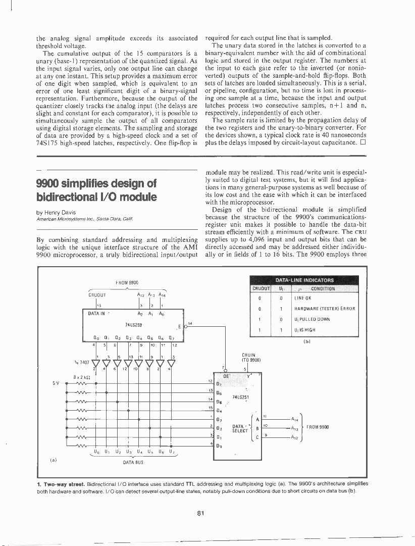
the analog signal amplitude exceeds its associatedthreshold voltage.
The cumulative output of the 15 comparators is aunary (base -I ) representation of the quantized signal. Asthe input signal varies, only one output line can changeat any one instant. This setup provides a maximum errorof one digit when sampled, which is equivalent to anerror of one least significant digit of a binary -signalrepresentation. Furthermore, because the output of thequantizer closely tracks the analog input (the delays areslight and constant for each comparator), it is possible tosimultaneously sample the output of all comparatorsusing digital storage elements. The sampling and storageof data are provided by a high-speed clock and a set of74S175 high-speed latches, respectively. One flip-flop is
required for each output line that is sampled.The unary data stored in the latches is converted to a
binary -equivalent number with the aid of combinationallogic and stored in the output register. The numbers atthe input to each gate refer to the inverted (or nonin-verted) outputs of the sample -and -hold flip-flops. Bothsets of latches are loaded simultaneously. This is a serial,or pipeline, configuration, but no time is lost in process-ing one sample at a time, because the input and outputlatches process two consecutive samples, n + 1 and n,respectively, independently of each other.
The sample rate is limited by the propagation delay ofthe two registers and the unary -to -binary converter. Forthe devices shown, a typical clock rate is 40 nanosecondsplus the delays imposed by circuit -layout capacitance.
9900 simplifies design ofbidirectional I/O moduleby Henry DavisAmerican Microsystems Inc., Santa Clara, Calif.
By combining standard addressing andlogic with the unique ir terface structure9900 microprocessor, a truly bidirectional
multiplexingof the AMIinput/output
module may be realized. This read/write unit is especial-ly suited to digital test systems, but it will find applica-tions in many general-purpose systems as well because ofits low cost and the ease with which it can be interfacedwith the microprocessor.
Design of the bidirectional module is simplifiedbecause the structure of the 9900's communications -register unit makes it possible to handle the data -bitstream efficiently with a minimum of software. The CRU
supplies up to 4,096 input and output bits that can bedirectly accessed and may be addressed either individu-ally or in fields of 1 to 16 bits. The 9900 employs three
5V
FROM 9900
CRUOUT Al2 A13 A14
113 I3 I2 1
DATA IN A2 Al
74LS259
A0
(10 0, 02 03 04 05 06 a,
E
4
1/6 7407
2
8 x 2 kS2
5 6 7 9
13 11
10 12
4 6VVVVV1210 8 2V4
140
U0 U, U2 U3 U4 U5 U6 U
DATA BUS
CRUOUT
DATA -LINE
Ui
INDICATORS
CONDITION
0 0 LINE OK
0 1 HARDWARE (TESTER) ERROR
1 0 lli PULLED DOWN
1 1 1.1i IS HIGH
(CTROL 91N900
7
OE
3
D,
0674LS251
05
04
A14
2
0310
A13DATASELECT
FROM 9900023 9
Al24
Do
1. Two-way street. Bidirectional I/O interface uses standard TTL addressing and multiplexing logic (a). The 9900's architecture simplifiesboth hardware and software. I/O can detect several output -line states, notably pull -down conditions due to short circuits on data bus (b).
81

WRITE
FROM 07 OR Do
13
74LS3678 -BIT SHIFTREGISTER
A13 A14 A15
3 2
DATA IN A2 Al A0
74LS259
ao Q1 Q2 03 04 Q5 a6 Q7
E 0
5 6 7 9 10 11 12
1 3 5 13 11 9 1 31,67407 VVVVVVVV2 4 6 12 10 8 2 4
8 x 2 k12
14
TO 07 OR Do
74LS367
7
2
13
-AAA,-WA
14
15
3
Up U1 U2 U3 U4 U5 U6 U7
DATA BUS
OE
74LS251
11
READ
10
A14
A13
Al2
FROM 9900
2. Easily mated. I/O unit can interface with other processors, such as the 6800. Software requirements will be more stringent, however; theymust provide for serial -to -parallel and parallel -to -serial conversions. Also, each bit must be mapped into one byte.
dedicated I/o pins (CRUIN, CRUOUT, and CRUCLK) andhas 12 -bit capability (lines A3-A14) of the address busfor interfacing with the CRU system. The processorinstructions controlling the CRU (SBZ, SBO, TB) canrespectively set, reset, or test any bit in the CRU array ormove the bits between memory and CRU data fields.
In the circuit example in Fig. la, the 9900 is used toperform an 8 -bit parallel -to -serial conversion for datathat is to be written on the data bus, from the micropro-cessor through the 74LS259 addressable latches. Duringall read operations, the 9900 converts the serial datastream emanating from the 74LS251 eight -channelmultiplexer (which receives the bus data) into a parallelword so that it may be processed.
As for the software, the bit instructions SBZ, SBO, andTB control a single processor -to -I/o data line, selectingthe address corresponding to the bit desired and execut-ing the required bit setting or bit test, as the case maybe. Multibit transfers are implemented by the processorusing the LDCR and STCR instructions.
Whether in the read or write phase, the startingaddress of the CRU field to be transferred should first beloaded into the base -address register. This address is theleast significant bit of the CRU field to be acted upon bythe software. Next, data should be transferred in theappropriate direction (system memory to I/o interface orinterface to memory) by reading or writing each I/O linein succession, under automatic processor control. The
LDCR output of the CRU initializes the shift of the desiredfield from the memory to the I/O, through a register inthe 9900, if in the write phase. The bits corresponding tothe field to be transferred are then shifted out onto theCRUOUT line, which is connected to the 74LS259. Thenoninverting, open -collector buffers (7407s) protect thelatches from short circuits on the data bus.
To use the I/o module for read -in, a logic 1 (high)must be written onto the corresponding output line to beexamined (from the processor through the 74LS259).This will cause the 7407 to be pulled low if the data busline is at logic 0. The CRUIN line can then be read usingthe STCR instruction.
The CRUIN line may be used to verify an outputcondition, making it easy to detect short circuits on thedata bus. The procedure is to set all lines high, lowereach in succession, and then read the lines to check formultiple lows. The table (Fig. 1b) outlines the variousinput/output conditions.
The circuit may be easily modified to work with otherprocessors. For instance, Fig. 2 depicts such an arrange-ment for the 6800 microprocessor. A greater burden isplaced upon the software here, because the programmust perform the serial -to -parallel and parallel -to -serialconversions.
82

Window generator increaseslogic analyzer's capabilityby Colin GylesCanadian Marconi Co., Montreal, Canada
Although the diagnostic power of the logic analyzer isunparalleled for troubleshooting digital systems, its abili-ty to detect the type of errors that lead to intermittentcircuit failures leaves something to be desired. For exam-ple, the analyzer would have difficulty in detecting arandom error in a computer system that passed data inshort bursts separated by longer periods containing no
relevant information. In such instances, this circuit vast-ly increases the recording range of analyzers of thetime -domain variety, such as the Biomation 8100D.
It is necessary to understand the operation of a stand-alone analyzer to appreciate the difficulties involved inthe display of certain data errors. In the example shownin the timing diagram of Fig. I a, a strobe or similardata -request signal is sent from a computer or othercontrol unit to a peripheral device. The peripheral thensends the data requested to the computer through thelatter's 1/0 port. Note that the data has a glitch, perhapscaused by noise, so that when checked by the computer itis found to contain an error.
There are two methods of recording the error with ananalyzer. The first method makes use of the analyzer'spre -trigger mode. Input data is recorded continuously,
DATA -IN STROBE(REQUEST) TOPERIPHERAL
DATA FROMPERIPHERAL TOCOMPUTER(I/ 0 BUS)
(a)
MODE
r1
GLITCH
LOGIC ANALYZER OPERATION
1-4- 2000
"4-'It P
t -0-
ANALYZER TRIGGERGENERATED BYCOMPUTER ONDETECTION OF ERROR
PRE -TRIG SAMPLES DISPLAYED
AUTO -ARM ANALYZERTRIGGER
2000 SAMPLES DISPLAYED ..2000 SAMPLES DISPLAYED --sH COMPUTER
HALTED ONDETECTIONOF ERROR
1-1 ANALYZERl'OESTROYED ON NEXT TRIGGER)TRIGGER
WINDOWWINDOWTRIGGER
\,..,..WINDOW
N SAMPLES TRIGGERRECORDED \*.
WINDOWN SAMPLES TRIGGERRECORDED ,-.....
N SAMPLESRECORDED
(b)
DATA -IN STROBETO PERIPHERAL
DATA FROMPERIPHERAL(I/O BUS)
(c)
I Is.____1 i
GLITCH
FIRST IWINDOW I LAST
WINDOW
5_1
N SAMPLES N SAMPLES-1 14- -01 14- -bi N SAMPLES I -4-
1. Analyzer overview. In typical example, stand-alone logic analyzer records glitch in the last word received on computer I/O bus only,because of limited record range (a, b). Record range is vastly extended with window generator, which produces bursts of clock pulses duringdata -strobe time, permitting many data words to be recorded. Errors occurring in other than the last word received can thus be detected (c).
83
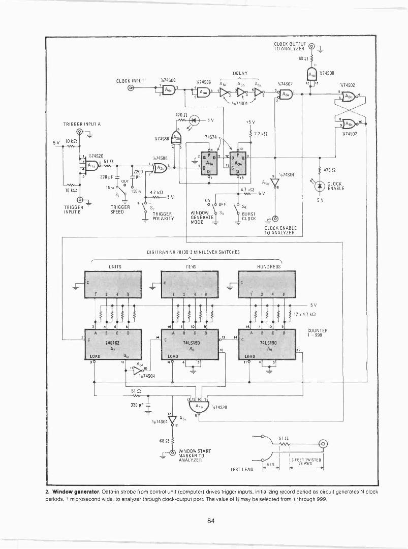
5V
TRIGGER INPUT A
10 k52
Y274S20
6 51 52
10 k52
TRIGGERINPUT B
CLOCK INPUT %74S08
%74S86
%74S86
2200220 pF pF
1 -OUT
15 ns0
S)_ 100 ns
TRIGGERSPEED
D
4.7 k52
3
3
DELAY
%74S08 Asa4
CLOCK OUTPUTTO ANALYZER
A55 A6c %74S02
MI6 5 3:0
470 E2
4
5V
POLARITY
S2
TRIGGER
W 5 V
6 0;/
5
74S74
410' 0
A3.
4
1674504
+5 V
2.2 k52
" u P aA3b
CL
9
68 12
iz 13
'474S08
%74S02
9
ONO OFF
WINDOW S3
GENERATEMODE _
9 '674SO4
A5dVre4.7 kE2mn 5V
ID
BURSTCLOCK r-Cs
CLOCK ENABLETO ANALYZER
5V
470 E2
%74S02
CLOCKENABLE
DIGITRAN NR 28138-3 MINILEVER SWITCHES
UNITS
1 2
TENS HUNDREDS
1 2 1 2 4
A B C D
745162
A7
LOAD Up
9 11 A5t
'/674SO4
10 9 15 1 10
A 8 C
7413190
A9
LOAD
4 5
3 1
5V
12 x 4.7 k52
A B
LOAD
74LS190
119 4
COUNTER1 - 999
51 E2
330 pFIL674504
68 E2
12
13112 10 9
Alb Y:74S20
WINDOW STARTMARKER TOANALYZER
TEST LEAD
51 E2
3 FEET TWISTED.126 AWG
2. Window generator. Data -in strobe from control unit (computer) drives trigger inputs, initializing record period as circuit generates N clockperiods, 1 microsecond wide, to analyzer through clock -output port. The value of N may be selected from 1 through 999.
84

and the analyzer is made to display the events causingthe glitch. In the case of the 8100D, it displays thesequence of states that occurred in the interval, 2,000sample units long, immediately preceding the triggergenerated by the computer when the error was detected.Each sample unit corresponds to the period of thesampling rate of the analyzer's internal data clock. Thus,if the clock period is 20 ns, the events occurring up to 40its before the trigger can be displayed.
Needless to say, the larger the required recordingrange, the poorer the resolution and the harder it is todetermine where an error occurs. And if the computer isso occupied with other duties that it cannot generate atrigger quickly enough after the error has occurred, theerror will be missed altogether. Thus the time At, shownin Fig. 1 b, must be minimized.
The second error -detection method uses the analyzer'sauto -arm mode, which when triggered by an errorrecords the following 2,000 samples. The circuitry is thenrearmed. If a second trigger should occur, the analyzerdestroys the previously recorded data and overwrites itwith 2,000 new samples. The results of its operation areillustrated in Fig. 1 b, with the trigger generated by theleading edge of the data -in strobe. With this method, therequired range over which the analyzer records is small,so that the resolution will be high.
The error -detection problem cannot be solved satisfac-torily by either method when the error is not containedwithin the last word received in a data stream (Fig. lc).This condition might occur if the computer were makingcheck -sum error determinations on a block of data froma paper -tape reader, where the results of the check wouldbe revealed after the data word was read. In mostinstances, it would be impossible to display the error,since the time between strobes for a reader might be 100milliseconds or so, but the strobe width might be only 1microsecond.
Thus, to record a block of, say, 10 words, the recordrange would be 10(100 ms) = 1 second, but the resolu-tion would be only 1/2,000 = 0.5 millisecond, and it issafe to conclude that an error lasting 1 is would not bedetected. Ideally it would be desirable to record theperiod in the vicinity of each strobe, where the errorwould occur, while holding the analyzer's internal clockoff during the remaining time.
Therefore to detect the error, it is necessary to gener-ate windows greater than 1µs wide by a counter deliver-ing N pulses to the external clock input of the analyzerafter each window trigger, where N could be selected bythe user. Then, on receipt of a trigger from the comput-er, due to detection of an error, the analyzer will stoprecording (assuming pre -trigger mode) and display2,000/N windows. The recording range would be equalto 4 seconds if N = 50 (that is, R = 100 ms [2,0001/50)for a resolution of 20 ns (equal to the analyzer's clockrate). This is an improvement of 100,000 times over the40-µs recording range previously shown to exist for thesame resolution.
The window -generator circuit for attaining the desiredrange magnification is shown in Fig. 2. The clock inputis driven by a square -wave generator to provide thedesired sampling interval. The logic analyzer is clocked
by the signal emanating from the clock -output port.When a transition of the required polarity occurs ateither of the trigger -input ports, the unit counts N clockpulses to the logic analyzer, N being set by the digitalswitch, which has a range of 1 to 999. During the time ofthe N -clock pulse burst, the trigger -input port is
disabled.The end result of the unit's operation is that N
samples are clocked into the analyzer after eachwindow -generator trigger. If the analyzer is set in thepre -trigger mode, then on receipt of an analyzer triggerfrom the computer, the recording will stop, displayingthe last 2,000 samples, made up of 2,000/N windowsside by side.
The window -start marker output may be fed to anyone of the eight analyzer channels. This pulse is oneclock period wide at the start of each window so thateach frame may be identified at will. The clock -enableoutput can be recorded on a second logic analyzer tomeasure the time between window frames, if desired.
Note that the analyzer can be used in all triggermodes while using the window generator. In any of thepost -trigger modes, the recording is complete when all2,000 samples have been taken. If there are not a suffi-cient number of window triggers, the analyzer will hangup. The burst -clock switch is therefore included toenable the recording cycle to be completed manuallywhenever there are too few triggers to record the 2,000samples.
The circuit relies mostly on sequential logic, as shown.SI and S2 select the trigger speed and polarity, respec-tively. A positive transition at A3a's clock input brings itsQ output low. At the next positive transition of the clockinput, A3b moves low. A4b and As; provide delay, inorder that Abe be enabled when the clock input is low.This is to prevent generation of a narrow clock -outputpulse, which could upset the analyzer operation. Theclock -output port now follows the clock -input signal. Thecircuit is designed to minimize the delay from the trig-ger -input pulse to the time the first clock -output pulseappears.
Just prior to the first clock at A6a, the flip-flop A6b-A6awas set, which enables counters AB and A9 to be loadedwith the digital switches. A7 is loaded during the firstpositive clock -input transition. This data is the 9'scomplement of what is displayed. Abc is then set high,and the counters are free to advance from their setvalues up to 999, at which time the counters enable Alband preset A3a to logic 1.
During the next clock input, A3b moves high. Thedelay provided by Agb and Asa-A5c disables A6. beforethe clock -input transition arrives at its input, thus ensur-ing that no narrow glitches can be produced at clockoutput, as mentioned previously. The logic present at theoutput of A3b then sets A6b-A6a, removing the presetsignal from A3a so that the trigger can be enabled for thenext window.
Lead lengths should be minimized when building thecircuit. The test lead for the trigger -input port should bebuilt carefully also. It should not exceed 4 feet in length.A 51 -ohm resistor on thi hot side of the test lead willminimize ringing and reflections of energy from probed
85

circuits. Twisted -pair wires should be used to avoid error between 33 and 60 MHz, which simply increases the
undesirable coupling effects. window size by one. The size of the window does not
The circuit can work up to 60 MHZ, with a one -count substantially affect circuit accuracy.
Synchronous pulsing cutsthree-phase motor's dissipationby D. J. GreenlandCambridge, England
At very low clock rates, below 20 hertz, the windings of athree-phase motor dissipate excessive power. But thisproblem may be overcome if the motor is not heavily
loaded-that is, the torque is less than 20 gram -centimeters. The circuit described here momentarilyswitches on the motor's supply line synchronously withthe phase -generator clock pulse that activates each wind-ing in sequence. Pulsing the windings at a low duty cycleand at the start of each phase increases circuit efficiency,yet enables the motor to develop sufficient torque.
Consider the savings in power. If each winding has adc resistance of 15 ohms and is periodically energizedfrom a 28 -volt source, the power dissipated by eachwinding as the clock rate approaches zero is P =(28)2/15, or 52.26, watts. Even when working at 20hertz, or a 50 -millisecond period, each winding would beenergized for the same 50 ms or so and the powerconsumed per phase would be P = (282/15)(50)(10-3)
= 2.61 w. But if the energizing time can be reduced to1 ms, say, the power consumed will be P=(282/15)(1)(10-3) = 52.26 milliwatts.
The energizing time, Tc, is controlled by elements Rand C of the 74121 monostable multivibrator, AI, asshown in the figure. The one-shot is driven by the samephase generator clock, OcK, that also drives the three-phase switching circuit. (Since many well-knownarrangements exist for deriving the required phase volt-ages for the windings, the actual schematic for thenetwork is not shown here.)
AI fires on the positive edge of Oa( and generates a1 -ms pulse that charges CI, switches Q1, and brings itscollector to 28 v. Q2 then turns on, driving the particularwindings that happen to be activated at that instant bythe switching network. The 0 output of A, then movesback to 1 after the 1 -ms interval and CI dischargesthrough R2 exponentially. CI, RI, and R2 are selectedonce the frequency of OCK, R, and C are known.
It should be mentioned that at clock rates above 1
kilohertz, this circuit offers no power -saving advantage.This is because the period of 1 -kHz waveform is 1 ms,comparable to the duty cycle required to reduce thedissipation for the 20 -Hz clock previously discussed. Li
OCK
OCK
5V
10
Al
74121
G1 J02
o,
Vol
50 ms
R,R1 «R>
I
c,
=1 msV = 28 e ' R2c1
28 V-
6 V
28 V 02
2N4237
6V
2N5961
OCK
3 x 2N4237
3-PHASESWITCHINGNETWORK
o,
02
1k12
03
1k12
Conservation. Power -pulsing the windings of three-phase steppingmotor at a low duty cycle and at the start of each phase cuts motor's
internal dissipation while developing sufficient torque for mediumloads. This technique is especially useful at stepping rates approach-
ing dc, where motor -overheating problems are notorious.
86

Small interface simplifiesprocessor interrupt routineby Robert ShanafeltLos Altos, Calif.
The closing and opening of an assigned key triggers anexit from the memory -resident display- and keyboard-strobing routine supplied in National Semiconductor'spopular SC/MP keyboard kit. But often the SC/MP micro-processor needs to respond to a signal not initiatedthrough the keyboard, such as a transmit/receive inter-rupt when the kit is used to control a transceiver. A wayout of this difficulty is to transform the interruptcommand into a simulated key closure by means of asmall hardware interface. Built out of a dual one-shotand four NAND gates, this interface not only simplifieshardware design but also keeps the amount of softwarethat will be needed for servicing the interrupt to aminimum.
As indicated by the figure, depressing the microphonekey initiates the transmit interrupt request to theNS10586 keyboard -to -microprocessor board that comeswith the kit. The event causes Al to generate a positive-
going, 16 -millisecond pulse. This pulse first combines atNAND gate G3 with the digit -1 strobe from G2 thatinterrogates keys A, 8, and 0 (line P55) of the keyboardmatrix. The result is then transferred through the wired -OR logic configuration of G1-G3 to column 1 on thematrix (line P39). At column 1 a negative -going pulse isproduced that is synchronous with the digit -1 strobe andis identical to the pulse that would be generated if the Akey on the keyboard matrix were depressed.
When the microphone key is released, A2 generates apositive -going pulse for long enough (16 ms) to overcomethe effects of switch bounce. The transfer of this pulse toline P39 is similar to the process previously described,except that gate G4 is activated instead of G3, corre-sponding to activation of the B key.
The program required to produce the interrupt requestis shown in the table. It is written so that a light will turnon when the circuit is in the transmitting mode and willturn off when the circuit is in the receiving mode. Inadvanced applications, the program steps that turn onthe light could be replaced with coding that would fetchthe transmitting frequency corresponding to the channelinput, display it, and present it to the frequency synthe-sizer for the transmitter, while the code that turns off thelight could be replaced with coding that would do thesame jobs for the receiver.
An advantage of this scheme is that during program
2.2 k2
5V
10
t A,
%74123
D
Ia
47 kS2
4.2' 11.,F
3 1
4
PUSH-TOTALKMICROPHONEKEY
_r 4
A2
h74123
a
47 kS2
1µF
5
4.7kS2
4.7 k2
TOMICROPROCESSOR
3
5
9
VIE
-can2 co -
7401
0
5V1
10
4
4 x 5.1 XS -2
P45 COL 8
P43 C 0 L 4
P27 SEG G
r KEYBOARD MATRIX -110 11 12 13 p 17
-F
P41 COL 2
P39 COL I
91 10
14
13
/2
CO
20 5
6
13,16
0
bt bf 1 1F bt
bt
1F 1 1 1 1 1-
LLA LB g i
of 1F It jt I
'55 DIG I
02 P53 DIG 21
3
.4' 4
'I 506
3 P51 DIG 3
04 P49 DIG 4
05 P63 DIG 5
06 P61 DIG 6
7 P59 DIG 7
7 0e P57 DIG 8
9
.1111M11
00
0
2
NS10586
Simulated keyboard interrupt. Two one -shots and four NAND gates transform transmit/receive command into an apparent keyboardclosure for SC/MP microprocessor. Only three interconnections to the microprocessor board are required. The small interface simplifieshardware design and keeps the amount of software needed for servicing the interrupt to a minimum (see table).
87

RAM location Code Mnemonic
SC/MP INTERRUPT ROUTINE
Comment
C4 LDI-0-0F20
OF21 01 01
OF22 37 XPAH Load 0184 into P3 register, which is starting point of keyboard
OF23 C4 LDIstrobe and display routine.
OF24 84 84
OF25 33 XPAL
OF26 3F XPPC } Start keyboard strobe and display routine
OF27 90 JMPJump if either GO, TERM, or MEM key pushed
0F28 00 00L}0F29 C4 LDI
OF2A OA OA
/Test if A key pushed
OF2B 60 XRE
OF2C 9C JNZ
05 05 1If not A, jump to OF33
OF2E C4 LDI
rOF2D
OF2F
O
F31
F30
00
07
90
00
CAS
JMP 1
/Set flag 1 low (turn light off)
Jump to OF2047 OF32 ED --19
4-0F33 C4 LDI
OF34 OB OB Test if 8 key pushed
/OF35 60 XRE
OF36 9C JNZ
OF37 E8 -24 }If not 8, jump to OF20
OF38 C4 LDI
OF39 02 02 Set flag 1 high (turn light on)
OF3A 07 CAS
OF3B 90 JMP
1
Jump to OF204 OF3C E3 -29
development, interrupts may be simulated simply bypressing the A or B buttons on the keyboard matrix. Insome cases, though, it would be better to use thecommand keys GO, MEM, and TERM for the interrupts,because they return the program counter to the nextprogram step instead of skipping over two program steps.
In the latter case, a JUMP command might be needed forrepositioning the program counter to the desired loca-tion, depending upon the program requirements. Notethat in no instance could the ABORT command be used,because program execution would terminate on thisinstruction. 0
Badge reader checksfor production defectsby K. C. HerrickESI Electronics Corp., San Francisco, Calif.
Though production testing of electronic products usuallyinvolves only a set of simple individual tests, the repeti-tive measurements that must be made require muchmanual switching to connect the test circuit to identicalpoints in each device. The small perforated -card (badge)reader described here, however, will eliminate much ofthe labor of constructing test -set fixtures by enabling asingle set of cards, each of which is individually coded
88

for a specific test, to set all switches automatically.The most useful type of badge reader for testing
purposes is the bed -of -nails variety. In this reader, anarray of metal pins is clamped against an inserted cardto sense hole or no -hole status at all possible holepositions simultaneously. Typical readers contain 100 to240 hole positions and include a switch at each positionthat is activated if a hole exists there. Actuation of thereader either is automatic, using a solenoid, or requires aspring -release, which is cocked by prior actuation of acard -ejection lever. The readers are readily availablefrom AMP, Sealectro and others, and some are availableon the surplus market.
A hand punch can be used to punch holes in a card inany desired configuration. A set of cards is thenprepared for each test performed. Only a single readerneed be used if the reader's sensing and control circuitsare connected to standardized connectors. The specifictest setup for each item to be checked is then configuredwith mating connectors so that the reader can be easilyplugged into the desired test jig.
The reader's sensing switches may be wired in almostany configuration, because both sides of each switch areisolated. In general, however, it is advantageous to createa switching matrix that is bused along one axis, yielding,for example, 10 individual switches making contact toeach of 12 buses. Far fewer wires need be brought to aconnector when the busing technique is used.
The usefulness of a small card reader may be illus-trated with a simple example in which 15 identicalcircuits have to be tested on each item. Each circuit is tohave one balanced input port and one output port. Bipo-
lar circuit potentials must be applied and measured.Because the input to each circuit is balanced, inputsignals must be applied separately. Only the input linesand power line may be bused. Also, 15 diodes must betested for their forward voltage drop and the peak -inverse voltage they can withstand.
Wiring up a conventional manual -switch test jig wouldrequire much labor and several multiposition switches.Consider how the card reader would be used instead.
Each of the 15 circuits may be looked upon as a blackbox with seven leads, of which the first two represent theinput port, the third and fourth go to measuring instru-ments, and the fifth represents the output. Each of the15 diodes can be accessed via the sixth (cathode) andseventh (anode) terminals.
A 12 -by -10 -switch matrix (Fig. la) may be used inthis example. The matrix lines or points are designatedby letters or letter pairs A-Z or AA-EV, each ofwhich denotes a bus or switch point. Note that columnsare bused, but switch contacts in the rows are individu-ally connected to the wire denoted by the letter orletter pair. The leads of each circuit to be connected to aswitch or bus are given by a designation in the areabelow and to the right of a given cross -point.
Conductor 1 of each circuit is assigned numbers 1-1 to1-15. Conductors 2 through 7 are similarly assigned n-1to n-15. Because each bus has only 10 contacts, twobuses must be assigned to accommodate all leads 1 and2. Thus lines A and B of the matrix are tied together,and so are lines C and D.
The signal source driving the circuits' input designated8 and 9 is not connected directly to the buses, but rather
E E E E E E E E E E E EH\J\K\L\MNP RS T U V1-9 1-10 2-9 2-10
D D D D D E E E E EE EV\W\X\Y\Z A BCD E F G1-8 1-11 2-8 2-11
D D D D D D D D D D D D
G\ H\ J\ K\ L M NPR ST U1-7 1-12 2-7 2-12
C C C C C C C D D DODT\U\V\W\X Y Z A B C E F1-6 1-13 2-6 2-13CCC,CCC C C C C C C
E\ F\ G\ H\ J K L M N P R S1-5 1-14 2-5 2-14BBBBEIBEIBBCCC
R\ S\ T\ U\VWXYZABD1-4 1-15 2-4 2-15
B BBB BB BBB BBBC\ D E\ F G H J K L M N P
1-3 2-3A A A A A A A A A AB El
P\ R S\ T U V W X Y Z A B1-2 2-2
A A A A A A A A A A A A
B\1 CDEF1
\-12
GHJK LMNNPR S TU VW X Y Z A\ \ \ \ A8 9 8 9
0 0 0 0 0 o 0 0 0 0 0 0A___13,CDEFGHJ KLM(a) CARD ENTRY (TOP VIEW)
(b(
7-1 - - -DIODEUNDERTEST
TEST -VOLTAGEINPUTS
DIGITALVOLTMETER
1. Automatic. A 12 -by -10 -switch matrix formed by card -reader contacts can be used to make production line test -jig checks (a).Programmed cards switch in balanced line inputs (and outputs) of seven -port circuits under test (see text), to be driven by external sources 8and 9 at lines A through D on matrix. Setup for checking diodes' forward voltage drop and inverse withstanding value is shown in (b).
89

2A
BADGE READER'S115-V ac SOLENOID
1N4004
1k52
2N5755
RESET 10052
1k52
POWER INTERLOCKPROTECTION FORCARD -READERCONTACTS
10 kE2dc- -MicYzicYzclfz-
+
50µF
2. Reader actuator. Control circuit for card reader that uses solenoid, such as Sealectro's model 0811-012-007, has relay delay that protectsreader contacts from excessive current should a short circuit exist in test jig. The relay also prevents pitting of reader's sensing switches ifcontacts make or break with current flowing. M represents reader microswitch that is activated by insertion of card.
to the field of the matrix, as shown. Then leads 1 and 2of the individual circuit boards are connected to theassigned matrix points.
Now, by punching a card at points AB, AD, N and S,an input signal of a given polarity can be applied to leads1 and 2 of circuit board number 1. By punching a secondcard at AB, AD, P and R, a voltage of the oppositepolarity is applied. In this way, all input connecting isdone by punching four holes in one card-two to selectthe signal polarity and two to select the individual circuitboard to be tested.
A circuit's measurement leads (3 and 4) and outputlead (5) may be accessed in a similar way, but becausepolarity need not be considered, test circuits may beconnected via the matrix buses. For instance, the outputdevice at lead 5 (perhaps a load or a meter) can beconnected to buses E and F, with leads 5 of the individu-al circuit boards connected to T, AF, AU, etc. Similarly,buses G and H should be tied together and then connect-ed to a meter (lead 3), and buses J and K should be tiedtogether and connected to the measuring instrument atlead 4.
Columns L and M of the matrix are used for diodemeasurements. One side of each diode is grounded, andits free end is connected to the matrix field. Extracontacts are available for applying two polarities of testsignal, and a digital voltmeter can be connected to busesL and M. The circuit is as shown in Fig. 1 b.
If holes AA and BB are punched on a card, the
forward drop for a diode will be measured by the digitalvoltmeter. If a second card is punched at Z and BB, thediode's reverse voltage will be measured.
For card readers that are operated by a solenoid, apermanent control circuit should be built. The one inFig. 2 serves well for a popular Sealectro reader.
With the example setup, all tests are done using 30cards and separate meters for 3, 4, and diode testing. Asingle meter could be used for all measurements if 92cards were used: a set of 30 cards would be required toaccess output lead 5, each of which, in addition to havingits normal complement of holes, would require a hole atV and a 3 hole in matrix column G or H. A second set of30 cards would access output lead 4. These cards wouldresemble the first set, except that hole X and holes incolumns J and K would have to be punched in addition.A final set of 32 cards would require holes only incolumns L and M for testing the diodes.
Blank cards can be obtained from at least one supplier(AMP), premarked with matrix -hole locations. AMP alsosells a hand punch. These accessories have on occasionbeen offered with surplus readers also.
The cost of a new badge reader could run from $150to $350. Surplus units can be obtained for as low as $50,and some of these units with cards and punches areavailable from the author.
90

Uniting number generatorsfor long bit patternsby Leonard H. AndersonSun Valley, Calif.
The length of a pseudo -random bit pattern can bepredictably extended if the rules for combining two ormore available sequence generators of given length areknown and applied. Fortunately, the interface requiredfor combining number generators is extremely simple,
often consisting of no more than one logic gate.Maximal -length sequence generators that use shift
registers normally have periods of 2" -1, where n repre-sents the number of registers used. Every such sequencehas a numerical length that is odd, but few lengths areprime (that is, most often the number can be factored).It is a property of the register to have recurring factorsthat depend on the n'h multiple. The table shows themaximum length for any n and the factors common toevery nth multiple from 2 to 47.
These factors enable the designer to determine wheth-er combining two or more generators of given length willincrease the total sequence length: two generators havingcommon factors tend to generate similar patterns during
40
3C 0
74._S14
0
90
11
CLR
A Al OH
90
'A 7 4 LS86
12
13
CLR
A A2
OD
QH
96
6
STAGE 13
3
CLR
A A3 QH
90
3
233-1 SEQUENCE GENERATOR
CLR
A A4
a
STAG E 33 --"r
13
100
11
Y:74L37412
90
'A 741S86
ecco
9
CLR
A A5 OH
OF
11
STAGE 7-
(2
1 kS2
+5V
I-- MANUAL RESETI
4
13
CLR
A A6 OH
90
225-1 SEQUENCE GENERATOR
CLOCK INPUT
CLR
A A,OH
STAGE 25'
13
NOTE: PIN 2 OF ALL SHIFT REGISTERS ANDPINS 1,13 OF 74LS74 TIED TO +5 V
Al 74LS164 8 -BIT SHIFT REGISTERS
13
PATTERN
5 )D6OUTPUT
'h74LS86
Extension. Nine -package circuit combines 33 -stage and 25 -stage pseudo -random sequence generators in order to extend pattern length to2.88x 10" clock periods. Generators' outputs are merged with one exclusive -OR gate. Combining generators of any length for long bitpattPrns is possible, provided rules for applying bit -pattern data (see table) to n -stage registers are known.
91

portions of their individual cycles, causing a departurefrom the pseudo -random output expected.
The factors for all sequence lengths have been foundby first factoring n, then finding all the possible productsof any and all factors, and finally consulting the table for
the nth -multiple sequence length. For a 224- 1 generator,n = 24 = 2.2.2.3. The n -factor combinations of 2.2.2.3are 2, 3, 4, 6, 8, 12, and 24; thus, sequence length factorsare 3, 7, 5, 3, 17, 13, and 241, respectively.
Now, if a 224- 1 generator is connected in series (cas-
BIT-PATTERN DATA - n -STAGE PSEUDO -RANDOM GENERATORS
n Sequence lengthSequence length factors
common to every nth multiple
2 3 3
3 7 7
4 15 5
5 31 31
6 63 3
7 127 127
8 255 17
9 511 73
10 1023 11
11 2047 23 89
12 4095 13
13 8191 8191
14 16,383 43
15 32,767 151
16 65,535 257
17 131,071 131,071
18 262,143 19
19 524,287 524,287
20 1,048,575 5 41
21 2,097,151 7 337
22 4,194,303 683
23 8,388,607 47 178,481
24 16,777,215 241
25 33,554,431 601 1801
26 67,108,863 2731
27 134,217,727 262,65728 268,435,455 29 113
29 536,870,911 233 1103 2089
30 1,073,741,823 331
31 2,147,483,647 2,147,483,64732 4,294,967,295 65,53733 8,589,934,591 599,47934 17,179,869,183 43,69135 34,359,738,367 71 122,921
36 68,719,476,735 3 37 109
37 137,438,953,471 223 616,318,17738 274,877,906,943 174,76339 549,755,813,887 79 121,369
40 1,099,511,627,775 61,68141 2,199,023,255,551 13,367 164,511,35342 4,398,046,511,103 541943 8,796,093,022,207 431 9719 2,099,86344 17,592,186,044,415 397 2113
45 35,184,372,088,831 631 23,311
46 70,368,744,177,663 2,796,20347 140,737,488,355,327 2351 4513 13,264,529
92
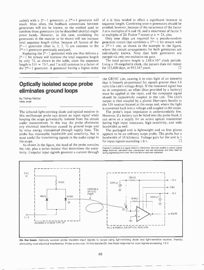
caded) with a 26- 1 generator, a 2" - 1 generator willresult. Most often, the feedback connections betweengenerators will not be known, so the method used tocombine these generators (to be described shortly) mightprove handy. However, in this case, combining thegenerators in the manner to be shown will not increasetotal sequence length either, because all factors of the26-1 generator (that is, 3, 3, 7) are common to the224_ 1 generator previously analyzed.
Replacing the 26-1 generator with one that delivers a29- 1 bit stream will increase the total sequence lengthby only 73, as shown in the table, since the sequencelength is 511 = 73.7, and 7 is still common to a factor ofthe 224- 1 generator. A generator having a higher order
of n is thus needed to effect a significant increase insequence length. Combining even -n generators should beavoided, however, because of the recurrence of the factor3 at n multiples of 6 and 18, and a recurrence of factor 5at multiples of 20. Factor 7 occurs at n = 21, also.
Only nine chips are required for a pseudo -randomgenerator circuit that combines a 2" -1 bit stream witha 2" -1 one, as shown in the example in the figure,where the circuit arrangements for both generators areindividually known. Note that both generators aremerged via only one exclusive-oR gate.
The total pattern length is 2.88 x 10'7 clock periods.Using a 10 -megahertz clock, the pattern does not repeatfor 333,600 days, or 913.347 years.
Optically isolated scope probeeliminates ground loopsby Vishay NetzerHaifa, Israel
The infrared -light -emitting diode and optical receiver inthis oscilloscope probe can detect an input signal whilekeeping the scope galvanically isolated from the circuitunder measurement. In this way the probe eliminatesany electrical interference caused by ground loops andby stray energy transmitted through supply lines. Theprobe has reasonable ismost useful for transferring signals in the audio range tothe scope.
As shown in the figure, the head of the probe containsthe LED, plus a series resistor that determines the sensi-tivity. Unipolar input signals generate a current through
the GE55C LED, causing it to emit light of an intensitythat is linearly proportional for signals greater than 1.6volts (the LED'S voltage drop). If the measured signal hasno dc component, an offset (bias provided by a battery)must be applied at the input, and the composite signalshould be capacitively coupled to the LED. The LED'Soutput is then coupled by a plastic fiber-optic bundle tothe 539 receiver located at the scope end, where the lightis converted back into a voltage and coupled to the scope.
The probe's input impedance is understandably low.However, if a battery can be fitted into the probe head, itcan serve as a supply for an active optical transmitterhaving high input resistance, high sensitivity, and widebandwidth as well.
The packaged unit is lightweight and on first glanceappears to be an ordinary scope probe. The probe has abandwidth of 10 kilohertz. Voltage gain for the unit is 1for input signals exceeding 1.6 v.
Engineer's notebook is a regular feature in Electronics. We invite readers to submit originaldesign shortcuts, calculation aids, measurement and test techniques, and other ideas forsaving engineering time or cost. We'll pay $50 for each item published.
r-(+)
( -)L
1N914 GE55C
HOUSING E-Z HOOK TYPE XP
1
CROFON-3OPTICALFIBER
F
0.041pF
130 kS2
20 MS2
7
0.047 pFl.
BELL & HOWELL 539 OPTICAL RECEIVER
I
+15 V
GND
15 V
SCOPE
On the beam. Optically isolated probe transfers input signals to scope using light -emitting diode and light-sensitive receiver, therebyeliminating most electrical interference. Probe works over 10 -kHz bandwidth, has linear response for input signals exceeding 1.6 V.
93

Single -wire pair multiplexespower and data for displayby Tommy N. TylerPowers Regulatory Co., Denver, Colo.
Using one decade counter per digit, this circuit multi-plexes both power and data to a remote digital displayover a single pair of wires. Implementing the circuit witha complementary -metal -oxide -semiconductor counterensures the multiplexer draws only microwatts of power,a level that can be easily supplied by the circuit's power -storage element while data is being sent.
The arrangement required for a single digit is shownin (a). The circuit automatically initializes the display atzero on power up.
During the hold time (b), power is supplied to the4033 counter via D1, and CI charges up to the supplyvoltage. Following the hold interval, Q1 turns off, allow-ing R2 to pull the reset pin high, clearing the counter.The reset is accomplished by holding the line voltage lowjust long enough for C2 to discharge and turn off Qi. C1
maintains power to the 4033 during this time.After 1 millisecond, Q1 turns on, and the number to be
displayed is transmitted through the data line as a seriesof pulses with a 10 -kilohertz burst frequency. These aresent directly to the counter's clock input. (Note that theyare too narrow for the reset circuit to respond to.) Thenthe hold interval is repeated.
The display reading is updated by resetting the 4033to zero and initiating a count again. By keeping the dutycycle of the data pulses very low, the display's supplyvoltage will remain essentially constant.
Multiple -digit displays require additional 4033s to becascaded. With a 1 -megahertz burst frequency, a four -
digit display can be updated in 12 milliseconds, morethan sufficient for ordinary viewing if the number ofupdates is at least two per second. Assuming fourupdates per second, the display will be steady 95% of thetime. The 4033 will source 5 milliamperes per segmentwhen operated at 9 volts, enough to produce fairly brightdisplays when MAN -3 devices are used. RCA applicationnote ICAN-6733 provides extensive information oninterfacing the 4033 chips with various displays. 0
12 V
D,
2N3904 C,VDO MAN 3
10
4033 12
DATADECADE 13
6 4009 15 COUNTERWITH
9© 7 -SEGMENTa, OUTPUTS 6
2N3904C
7
5
(a)
12 VHOLD
SS
(b)
C2 T
RESETRECOVERY
-. 1 msCOUNT UP/ AT 10 kHz
t
RESET
ms)
Time share. Decade counter enables multiplexing of power and data Ones with a single -wire pair (a). Power stored in C, during the firstportion of the cycle energizes 4033 during the time data is sent. The hold -count timing cycle (b) clarifies operation.
94

Digital strain gageeliminates a -d converterby N. Bhaskara RaoU. V C. E, Electrical Engineering Department, Bangalore, India
An up -down counter and several logic elements are usedhere to transform signals from a strain -gage transducerinto a corresponding digital output suitable for driving adisplay. Replacing the analog -to -digital converter nor-mally required for this application, the counter circuitnot only costs less but, more importantly, uses standardlogic devices normally found at hand in the lab.
A 555 timer, Ai, is used as an astable multivibrator(see figure) whose on time is T. = 0.685(R, + R2)C andwhose off time is Tb = 0.685R2C, where R, and R2 arethe resistances of two discrete transducer elementsmounted on a common surface. Their values vary direct-ly with the amount of strain applied. In this case, thenominal values of R1 and R2 are 120 ohms. Resistor r is
a 2-1 potentiometer that is used to zero the circuit (nooutput from the 555) under no -strain conditions.
R, and R2 are wired so that RI- R2 becomes a positivevalue when a strain is applied to them. When the outputof Ai is high, the 74192 counter (A2) advances up at arate of f/2, where f is the circuit's master clock frequen-cy and f/2 is derived from flip-flop A3.
When Al is low, the 74192 counts down at a rate of f.Thus, at the end of one cycle, the net counter readingwill be N = Ta(f/2) - Tbf, or:
N = 0.685f(R, - R2)C/2 = K(R, - R2)
where the scale factor, K, equals 0.3425fC. Thereforethe amount of stress becomes known when R, - R2 isdetermined. K can be set to any value by the properchoice of f and C. As seen from the equation, thesensitivity of the circuit increases as K is made larger.
As Al moves high at the start of the next cycle, onehalf of the 74123 dual one-shot, A4, is triggered andclocks the 7475 quad latch, A5. Thus the latch stores thecontents of A2. A6 converts the 4 -bit binary input into aseven -segment output for the display. The other one-shotin A4 then clears A2, and the new count cycle begins.
5V
Al
555
MASTERCLOCK
5V
1,10311
,4
12
5
K,, K2
Ji, .12
CLOCK
J ,K
A3
7470
0
67404
f/2
2
A4
'h74123
50 ns
13
14
5
'47432
6 4
4,13
CLOCKUP
CLOCKDOWN
A
CLEAR
A2
74192
3 2
3
5
6
7
7
4
10Y:74123
50 ns
CLOCKA5 7475
01 O2 03 D4
16 15 10
2
9
A6
7447
a bc d131l 121 1111OI 91,151 141
TO SEVEN SEGMENT DISPLAY
Stress test. Digital circuit transforms resistance change of strain -gage transducer R, -R2 into corresponding index without need for standarda -d converters. Number displayed represents R, -R2 scaled to a factor, K, that is equal to 0.3425 fC.
C-MOS tester checksfor assembly errorsby Joseph G. GaskillSolid State Scientific Inc., Montgomeryville, Pa.
Detecting most faults in complementary -metal -oxide -semiconductor devices due to errors in packaging orbecause of burnout while in actual operation, this testercan check virtually all the elements in the present c-moslogic family. The unit needs only to perform a set ofsimple open and short tests at each pin of the device toquickly check for chip failures.
Assembly -related rejects and in -circuit failures are
95
I, /4013B
3
FROMA5-15
Al
C
S
A2: 4011UB
11111-3 I 5r
50 kS2
4
200 pF
14CL A3
401713 C°''TCE RST 8"
131 15 9
TO
A16-62
5V
11:1"21 1µF-II
1START 1---
A14
45286
50 kS2
I 10 -F-2 kS2 15 14
6
5V
5V
2A14
50 kS2
10
10kS2
FROMA3-9
1.5 kS210 kS2
2
3
680.S1FROM
A6-3
200 S2
A6-1
A6-8
A7 1
A7-8
A8-1
A8-8
L6
Ag 1
A13-4
A9-8
A10-1
A10-8
A11-1
Ali 8
Al2-1
RANK C S
Al2 8
A
M311
A17
7
13
50 kS2.
50kS2
9
A4
CL
RST
Q
Q3
Q4
2
40246
111F50 kS2 50 kS2
H 10 -IId 15 14 10 82
A15
12
34528B
A15
13
5V
A18. 40111.18
01,
5V
23
r 7 F-71
A2
A
1I
1 .2
021
0. I
c
1 03
4 I 1
: 5056 6
7
1).
07
09RANK
0910 8
110 O012 d°
30 011
14 012
015 013 1
DITCH
IS, $2c S3c0 it
S4c
016014
L__J L__J16 PINS) (14 PINS
DEVICE UNDER TEST
9
0
12113 8 9
121 13
9
VA 19
10
FAIL
A19140016PASS
01
02
D3
04
A5
45156
ST
INH
S
S3
S4
S12
$13
$14
S15
5
9 6
12
5
A
3,9A6 3
8.11
2 10
8 6
12
5
A
39
8.11
2,1
.11Er
6
12
5
A8
3,9
1.4
8,11
2,
6
12
18 5
Ag
,11,
6
12
0 5
A10
9 6
12
14 5
Al
13 6
2
16 6
Al2
3 9
1.4
8111
2
RANK A SWITCHS1A
5
13
Al
A6 1
A6 8
A7 1
A7 8
AB 1 1-i
`7;A8-8 im-
- 1
-8
5A10-1 ctA10-8 LE
CJ
V)A11 1 0A -8
Al2-1A.2-8
2
9
4 8 10
r A13-1
5 kQ
TO A6-A13: 4416ABA1-3
S2A
S3A
S4A
SSA
S6A
S74
B SWITCH
°SIB
05213
S413
0 S38
S58
S68
S7B
14
N
$4
14
14
$4
5VA13-11
V V.
44
14
14
14
14
ALL DIODES: 1N914
A13-1
A13-11
Checking C-MOS. Tester checks for defects in C-MOS 4000 series devices. Device under test is placed in the appropriate test socket, therank switches set as given in table, and the start button depressed. Test results appear as active -high signal at pass or fail output.
96

SWITCH SETTINGS FOR C-MOS TEST SET
Switch rank A Switch rank B Switch rank C
Device 1 2 3 4 5 6 a 1 2 3 4 5 6 7 1 2 3 4
4000B ..... ......140016 000000 000000 04001D B ...... MM.... 1.140026 1.1.11.MM ..... .4006B II. 1111000 ......11111 1.114007UB MMEll 1.1 ....11. 11114008B 1.11.11............ III4009U B 111111.111111..M.NMI= M1. IIII4010 B .........11.1.1.1111 ... .4011 B ........ .111.10000 .4011 U 8l.M.1.11111M .1.11..11111.11 El40126 OliMMMM ...... 11140138 00001111.1 MM.... .4014 B IIIIIIIMMMI011111 IIMMIIMINIIM4015B .11.11.1....111...1111MM. ill4016B ...MEI. ....... 1114017 B .1111.1..........111. 11.40186 11111111111.M.11.111111.111111111.11111. I.40198 M=MMMINIMINIIIMMMMINI M4020B ...1.1111111........11 .4021B ................ 1.4022B 111000. . 11111111.11... .40238 .... ......... .40248 111111M000. . MI .4025B 11 INIMINIMMM MI4026B 1111............... I.40278 1111.1..11111....1111.... .40288 ....1.1...........1 MI4029 B MNIIIIIIII1111111111114030 B ........ ....... 1.114033 B ....1111.1.MM..... 1111.4035B ............... 111.4040 B ................ .4041 U B ....11.11. MM.... .1114042 B ...........001111111 I.4043 B ..111111111111111111..... 0111111 .114044B 1.1 .111........11111.1.11 .114046B 11......1111111.1.1.... .4049U8 M IN IIE mil4050B . . . . .11 11..1 M40518 MIIIMIIIMINIIIIMIIMIIIIIIIIMMM MI4052 B ..1.1110.11111.1....... I.4053 B 111.11....11.1.11111..... .4060B ......111.1111.....1111 .40668 ...... 1111111.1... . .40688 MI.. MM... .4069UB OM 11. 011.000. .
Switch rank A Switch rank B Switch rank CDevice 1 2 3 4 5 6 7 1 2 3 4 5 6 711 2 13 4
4070B .11.111...1. ...MEM M4071B ...... MM.... .4072B MIIIIIMMM 01111001111 .4073B 0001111111.1 0000.1.11 111140758 .111111...11111 ...... .40768 ..11.111111.1....11.1.111.111 1.1140278 00001.. ...MM. M40786 IMMIIIM ....11111 MI4081 6 111111111.... 11.01111... 1.114082 B MM.MMI 00001111 M4093B ......11 ..00001111 II.41 60 B ...11111111.1........11111. .111
MINIMIIINIMMMMIIIMIIIIIMIIII IM4161 B4162 B ................. .416313 .1.11.11.....11111111.1.11.1.. .44018 001110111. 11...... M.44 o 28 IIIMMMMM 0000. MI44048 MIMMINISMO . .... M441113 ...... 01.11.11.11.11. 1.14412B EM . MI4416e MIIIIMIEMI 11111111111101MM 1.144268 .11111,1111. .1111. 111.4428B ...... 111111.1.1.111111. 1.1MEN ....1111 M. I.4441U B MEI IMIM MM MI MI44456 EIM. . .11 1.11. .-44466 ....1.1111....... 11114449U B ..111111........ ... ME45026 M111111111111111MM 11.451013 111.11111.............. MI4511B .111..........111.1 MI45126 ..............11.111 11.145188 M.M....11.11.11111.1111...M ill4518B ................ -4520B .................. ' III45226 ....... .1.111111111.11111. III45268 .............11. .45278 .............. 11.4528B MMMINIIMEMEM11111.01.1. MIMI M45318 .1.1111.11111.1MM......111. .145438 MMINIMINIIIMMIMMIIMINIMMM M45558 1.1111111111.11.MIMMMM.Mill I.45568 ...............111 .45828 ..111.11.1.......... .4584 B 01101111.. 0000.1.11 1.4585B MINSIMMEINIIIIIINIMM
predominately caused by or result in internal shorting ofwires between leads or open bonds to device pads andpackaged posts. The detection of these failures is rela-tively simple for C-MOS chips because each input andoutput port is connected to two diodes internal to thedevice, one forward -biased with respect to the positive,supply voltage and the other back -biased with respect tothe negative supply. Hence it is necessary only to checkwhether each diode is opened or shorted. This, in princi-ple, is simple to do.
Most c-mos devices have at least 10 active ports,however, and consequently it becomes a problem todetect failures in many diodes while performing theminimum number of measurements. The proposed solu-tion arrived at for testing C-MOS devices having up to 16pins is shown in Fig. I.
Briefly, A2 serves as a gated oscillator operating at100 kilohertz for stepping A3, the 4017 decade counter,when the start button is pressed. A3 generates a strobefor circuit timing and also advances A4, the 4024 binarycounter, so that each location of the 4515 1 -of -16 -linedecoder can be addressed.
The decoder sequentially steps once througl- A6 -A13,the quad analog gates, each of which is wired as adouble -pole, single -throw switch. The output ports of the
4515 can thus provide a voltage for testing the diodes atall pins of the device under test.
Any transmission -gate output port connected to ashorted diode will move low. Open diodes will cause theoutput to float. The results of each individual diode testare monitored by window comparator A16 -A17. Thecomparator's output is then latched by A18 and passedinto either the pass or fail gate at the output.
Switches SIA-S7A, SIB-S7B, and S1c-S4c, the so-calledrank switches, which are connected to the test -socketpins, must be set accordingly to check the particulardevice desired. Required switch closures are presented inthe table for all 14- and 16 -pin 4000 -series devicesproduced by Solid State Scientific Inc.
Note that the 28 -diode matrix connected to the rankswitches must be individually switched into the circuit ofthe particular device under test. The matrix is wired sothat if there are any unused (inactive) pins in the device,the diodes will simulate the device's diodes; the open -short test may therefore be performed at each pin of thedevice without generating an erroneous response (that is,an open -circuit indication).
97

What happens to semiconductorsin a nuclear environment?
For designers who must select components to survive high-energy radiation,it's important to know how each type reacts
by David K. Myers, Fairchild Camera and Instrument Corp., Mountain View, Calif.
El Of all the many ambient conditions to which semicon-ductor devices are exposed, from a computer's air-conditioned room to under an automobile's hood, none isas demanding as the nuclear radiation encountered incertain military and space environments or in the nuclearindustrial field. Unhardened digital electronic equipmentcan fail when exposed to ionizing radiation doses of aslittle as 103 rads (Si) -out in space, for example, in theVan Allen Belt-or to a neutron fluence of as little as10" neutrons per square centimeter -near a nuclearreactor, say. (Rads (Si) stands for roentgens absorbeddose in silicon, while a fluence is defined as the timeintegral of neutron flux.)
Anyone engaged in designing circuitry for use in suchenvironments must be knowledgeable about theirdiffering effects on different semiconductor technologies.Exposure to high-energy radiation introduces primarystructural defects into semiconductor materials (andhence changes their electrical characteristics) in waysthat depend partly on the duration and type of incidentradiation and partly on that particular semiconductormaterial's resistivity, impurity types and concentrations,temperature, and carrier -injection levels.
The nuclear environments to be considered here are: Fast neutrons, which can permanently degrade gain inboth bipolar and metal -oxide -semiconductor devices andincrease the saturation voltage of bipolar transistors. Steady-state ionizing radiation (the total dose), whichcan increase leakage current in bipolar devices and alter
1. Radiation shift. In MOS and C-MOS devices, ionizing radiationalters gate turn -on voltage, changing the operating point radically. Inthe MOSFET curve shown, a threshold voltage change of almost 3 Vis observed after exposure of the devices to ionizing irradiation.
threshold voltages in mos and particularly complemen-tary-mos devices. The transient ionizing dose rate, which at a highenough level generates photocurrents in all reverse -biased pn junctions, causing changes of logic state inbipolar digital circuits and latch -up in c-mos devices.
Neutron effects
In general, it is only when neutron levels rise to 1010 to1012 n/cm2 (E = 10 kiloelectronvolts) that silicondevices start exhibiting changes in their electrical char-acteristics. The base transit time and the base width of abipolar transistor are the main physical parametersaffected by exposure to fast neutrons, as can be inferredfrom the degradation in current gain (hFE). Modernsemiconductor manufacturing methods measure neitherof these parameters directly, but do control hFE and thegain bandwidth product (1'0, from which base width canbe deduced.
MAXIMUM DOSE AT 12-V7. GATE BIAS = 3,000 RADS (Si)
laV1_-== 0.31
MAXIMUM DOSE AT 0-VGATE BIAS = 10°IAVT --- 0.31
2. Radiated RAM. Threshold -voltage shifts are a function of radia-tion dosage and bias conditions for 4,096 -bit n-MOS random-accessmemories. Units with gate bias fail at lower radiation levels than zero -
biased units. A 0.2 -to -0.3-V change in V, induces failure.
98

TABLE
Semiconductortechnology
Radiationenvironment
1: COMPARING
Discretebipular
transistorsand J-FETs
THE RADIATION
Siliconcontrolledrectifiers
SUSCEPTIBILITY
TTLLow-
powerSchottky
TTL
OF VARIOUS
Analogintegrated
circuits
SEMICONDUCTORS
C-MOS n-MOSLight -
emittingdiodes
Isoplanar IIECL
Neutrons (c/nm2 ) 1010-1012 1019-1012 10'4 1014. 1013 1015 1015 1013 >10'5
g..--:
2cs)cN
Total dose(rads (Sill
>104 104 106 106 5x 10⁴ -105
103-104 103 >105 107
Transient dose rate(rads (Si)/s)(upset or saturation)
103 107 5x 10⁷ 106 107 105 >108
Transient dose rate(rads (Sills)(survival)
1010 1010 >1010 >1010 >1010 109 1010 >1010 1011
Dormant total dose(zero bias)
>104 104 106 106 105 106 104 >105 >107
Burnout by EMPAn electromagnetic pulse from a nuclear event cancouple into a system's cables and antennas and createvoltage/current spikes that may fuse the metalizationon a semiconductor surface. Usually the interconnectsystem on a semiconductor device is a thin metal layer,only 10,000 angstroms or so thick, and will fuse at acurrent density of 106 amperes per square centimeter.Most integrated -circuit metalization stripe widths aredesigned to keep the current density below 105 A / cm2during normal operation, including worst -case testing.
EMP-induced burnout of semiconductor junctions istherefore a serious problem. But while it is a failuremode of semiconductor devices, it originates in thesystem design and not in semiconductor selection orreliability. The electromagnetic pulse must be shielded,filtered or shunted to ground.
Data available from Government laboratories andsemiconductor manufacturers on semiconductors sub-jected to neutron irradiation indicates that double -diffused, epitaxially constructed integrated circuits, bothdigital and linear, will function within their originalspecification limits to neutron levels of 5 X 10" n/cm2(E = 1 megaelectronvolt). This holds for diode- andtransistor -transistor logic, as well as for low -powerSchottky TTL. MOS circuits, whether n- or p -channel orc-mos, are majority -carrier devices and not susceptibleto neutron irradiation below 10" n/cm2.
The total ionizing dose
A steady state of ionization increases bipolar tran-sistor leakage current most markedly in low -current,large -area devices. But even under worst -case conditions,these increased leakages are not enough to cause circuitfailure at radiation levels below 105 rads (Si). Indeed, inmany cases, bipolar integrated circuits have functionedwell at levels in excess of 107 rads (Si). Tests run on DTL,TTL, and low -power Schottky TTL circuits reveal radia-tion -induced changes only above 106 rads (Si).
The effect of a total ionizing dose on mos devices ismore drastic. It permanently changes the crucialthreshold voltage, VT, which is applied to the gate of amos field-effect transistor to create the source -to -drainconduction path or channel. This change can be attri-buted to the buildup of a trapped positive charge in thegate -oxide insulator and to the creation of fast surfacestates at the interface of the silicon and silicon dioxide.The result is a marked shift in the operating point of adevice (Fig. 1).
Recent radiation tests indicate that n -channel mosdynamic random-access memories are very sensitive toionizing radiation, having a nearly 100% failure rate at3,500 rads (Si), regardless of manufacturer. Forinstance, the major failure mode of 4,096 -bit dynamicn-MOS RAMS is the incidence of decoders stuck in thelogic 1 state, which in turn is due to changes in thresholdvoltage that exceed the operating design tolerance.
Most current n-mos test data is derived from these 4-kRAMS, but other large-scale integrated circuits like16,384 -bit RAMS, microprocessors, and similar complexn-mos chips are also sensitive to continuous ionization,being manufactured according to similar design rulesand processing. Failure threshold is 1,700 rads (Si) for4,096 -bit dynamic RAMS and 1,000 rads (Si) for n-mosmicroprocessors.
Precise threshold voltage changes in n-mos units are afunction of dose and bias, as shown in Fig. 2. Under anormal + 12 -volt gate bias, shifts in VT of 0.2 to 0.4 vhave been observed at 3,000 rads (Si). Circuit analysisindicates that the n-mos electrical designs will tolerate achange of 0.2 to 0.3 v in VT without failing. Tests of mosdevices at zero gate bias (again, see Fig. 2) show theywill fail only with the approximately 0.3-v shift in VTcaused by a dose of 104 rads (Si).
Radiation -induced shifts in threshold voltage similarto those described for n-mos also occur with c-mossemiconductors. The operating design tolerance FAVTI isusually 1 v for commercial c-mos products, indicatingthat a dose of 104 rads (Si) is required to cause failure.Actual cobalt -60 irradiations of Fairchild Isoplanar
99

TABLE 2: RADIATION
Data source
SUSCEPTIBILITY OF EMITTER
Northrop
-COUPLED LOGIC
Sandia Fairchild
Pulsed ionizing radiation
Narrow -pulse transient failure level
Wide -pulse transient failure level
Permanent -damage failure level
3x10⁸ rads (Si)/s
1.1-1.4x10⁸ rads (Sil/s
not determined -greater than 1.5x10¹¹rads ISil/s
no tests performed 5-7x10⁸ rads (Si)/s
no tests performed
1011 rads (Bilismaximum level(flash X-ray equipment)
Neutron/gamma permanent damage
Mean neutron failure level
Total gamma dose
Observed neutron failure -level range
Device type tested
Transistor gain -bandwidth product (fT I
2.2x10¹⁵ n/cm2(1 MeVequivalent)
6.6x10⁸ rads (Si)
1.9-2.6x10¹⁵n/cm2(1 MeV equivalent)
MC1678 L4 -bit counter
2.0-2.5 GHz
1 x10¹⁵ n/cm2(1 MeV equivalent)
2.5x10⁷ rads (Si)
1x10¹⁵ n/cm2*(1 MeV equivalent)
custom IC fabricatedby TRW
1.5 GHz
1 x10¹⁵ n/cm2*(1 MeV equivalent)
107 rads (Si)
1 x10¹⁵ n/cm2*(1 MeV equivalent)
Isoplanar II, ECL F100101,F100117, F100102,F100141 and kit parts
4.5-5.5 GHz
Maximum radiation exposure level; no failures were observed at this level.
c-mos and other available c-mos devices cause devicefailures at above 5 x 10⁴ rads (Si).
If the c-mos design margin for VT is reduced forelectrical performance reasons, then the radiation toler-ance would be sacrificed. This is the case for certainc-mos circuits with a VT of about 0.2 v, which all fail atapproximately 2,000 rads (Si).
In general, improved tolerance of ionizing radiationcould be realized by use of hardened oxide manufac-turing techniques and circuit design modifications.However, though increasing the circuit VT operatingtolerance would raise the ionizing radiation failurethreshold, it would also adversely affect the power,speed, component density, chip size, and yield.
Loss of memory and latch -up
A transient dose of ionizing radiation creates a photo -current in any reverse -biased pn junction, such as thecollector -base junctions of transistors and the pn junc-tions used for isolation in standard bipolar integratedcircuits. These photocurrents can be large enough tocause digital circuits to change state, from a 1 to a 0. Butthough they may change the content of memories, theycause no permanent failure. For some programs, logicupset is acceptable, but survival at the specified transientradiation dose rate is required. Tests show that DTL, rrL,and low -power Schottky rrL devices will change logicstate above a dose 5 x 10⁶ rads (Si)/s and survive 1010rads (Si)/s.
These transient photocurrents can induce anotherphenomenon, known as latch -up, in those types of is thatcan be driven into silicon -controlled -rectifier action orsecond breakdown. In this situation, they force thedevice to latch into one state and remain there until thepower is interrupted or the circuit destroys itself.
Such radiation -induced latch -up has not been ob-served in digital or linear bipolar ics employing double -
diffused epitaxial fabrication methods and operatingwithin specifications. Fairchild has had over 140,000low -power DTL devices tested by outside contractors tolevels of approximately 1010 rads (Si)/s without a true
latch -up failure. Nor has any been observed in rrL,Schottky rrL, or bipolar operational amplifier andcomparator circuits.
Latch -up of triple -diffused la does occur. But thistechnology has not been used to manufacture commer-cially available circuits for over five years.
mos resistance to latch -up, on the other hand, varieswith the process used. The problem has not been foundto afflict n-mos devices, which lack the fourth junctionnecessary for SCR action. But junction -isolated c-mosics, which have that fourth junction, have been observedto latch up at dose rates as low as 3 x 10⁸ rads (Si)/s.When operated at 5 v in the latch -up state, c-mosdevices return to normal operation after the power hasbeen interrupted. But when operated at 10 v, they failcatastrophically because of latch -up.
It is worth noting that the latch -up dose -rate level ofc-mos devices varies with the manufacturer, device func-tion, and chip design: there is a very uniform suscepti-bility to latch -up for devices with the same function fromthe same manufacturer.
For bipolar devices, it is different. The radiation toler-ance of a generic bipolar family can be determined bytesting sample parts of the family, since circuit designrules and manufacturing processes are constant through-out. This theory has been tested and verified on low -power Schottky rrL ics manufactured by FairchildSemiconductor.
Low -power Schottky parts made by other is firmshave been tested using the same radiation criteria. Theseresults, with the Fairchild data, add to the overall confi-dence that a specific bipolar part type has a specifiedradiation tolerance irrespective of its source.
Only limited testing has been reported on the radia-tion tolerance of high-speed emitter -coupled logic. Adata summary of ECL failure threshold levels for variousradiation environments is presented in Table 2.Nevertheless, a preliminary comparison of ECL with anumber of other types of ics and discrete semiconductordevices (Table 1) indicates that ECL easily excels themall in radiation tolerance.
100

Easy impedance matching opensthe digital door to analog delay lines
Widely available new models, designed for simple interfacing,can replace complex arrangements of logic gates;
a few basic rules are the guide to practical implementation
by Larry Garde, Magnetic Peripherals Inc., Minneapolis, Minn.
El A new breed of delay line is attracting digital design-ers, for the units are designed to minimize the interfaceimpedance -matching considerations that proved soresistant to solution in earlier attempts at logic applica-tions. Moreover, the new lines boast incrementaltappings and come in the familiar 14- and 16 -pin dualin -line packages, rather than the bulky, oddly shapedpackages of earlier models. Thus, it is much easier tomake use of their inherent large bandwidth to processsuch discontinuous -boundary waveshapes as digital andswitching signals.
A standard product
The tapped delay lines in DIPS are widely available andcan replace complex arrangements of logic gates. Theycan drive or be driven by transistor -transistor logic,emitter -coupled logic, and other digital families that arecapable of delivering sufficient drive current. Happily, aknowledge of only a few basic rules is required forpractical implementation of these devices.
Several manufacturers now make what may beregarded as the industry -standard tapped delay line. Thetable gives typical characteristics for versions that intro-duce a signal delay of 10 to 150 nanoseconds. No matterwho the maker or what the delay time, cost is about $12apiece, dropping to $3 in lots of 1,000 or more.
Standard delay lines have either a 50- or 100 -ohmcharacteristic impedance, suited for ECL or TTL respec-tively. They require terminating resistors, which firstwere mounted on the printed -circuit board, external tothe delay line. However, this arrangement often createdmore problems with capacitive loading, reflections on theline, and so on. Now many of the standard delay lineshave built-in terminators.
For the units that still require add-on termination, asingle resistor or the Thevenin-equivalent (two -resistor)arrangement may be used. The two -resistor terminationis designed to reduce the current load on the unit drivingthe delay line.
Delay lines may be customized to provide a desired set
TYPICAL DELAY -LINE CHARACTERISTICS
tdTotal delay
Ins)
ttTap delay
Ins)
Maximum risetime (ns) Dc resistance
input tc1)?utputDistortion (%)
Impedance(n)
Totalattenuation
(%)
Totaltemperaturecoefficient
delay (ppm/°C)Prepulse
(a)Pulse
(b)Postpulse
(c)Input
TciOutput
Tro
10 ±1.0 1.0 ±0.25 3.0 5.0 1.0 ± 13 ± 13 ± 13100 ±10%50 ±10%
2 100(0°-85°C)
20 ±2.0 2.0±0.25 3.5 7.0 1.0 ± 12 ± 12 ±12
30 ±2.0 3.0 ±0.3 3.5 7.3 1.5 ± 10 ± 10 ± 10
50 ±2.5 5.0±0.5 5.0 11 2.5 ± 15 ±15 ± 15
100 ±5.0 10±1.0 6.5 23 1.4 ±13 ±13 ±13
150 ±7.5 15 ±1.5 8.0 30 1.7 ±13 ±13 ±13. . -
k WIDTH .---3td
Tri All data for minimum40-, - I.- -.
Eint
/
90%i
50% "
I
10%
input -pulse width = 3td
*
Eout
_i____÷.___
.4-- to -01
50%
10%
90%b+ b-
* iL -1----° a-
Troc+
101
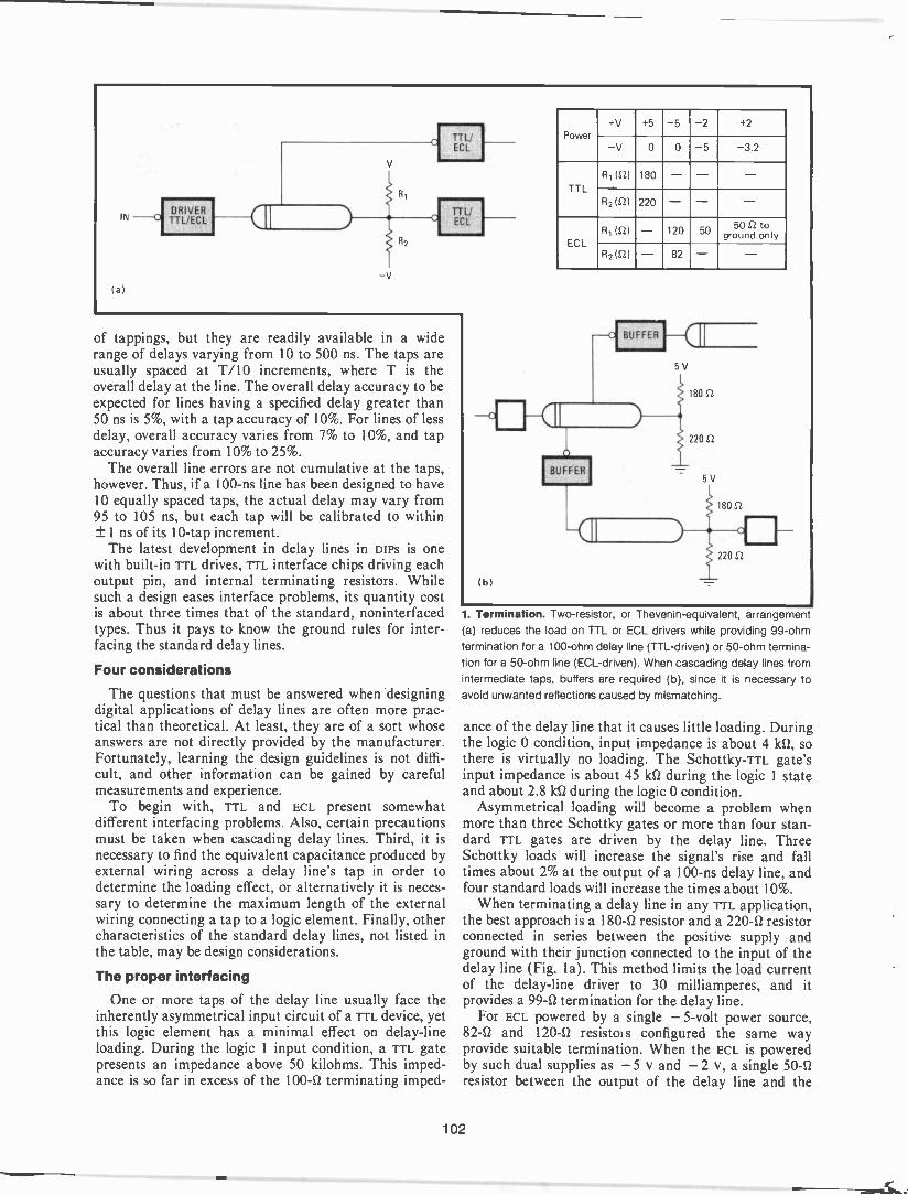
IN
(a)
DRIVERTTLJECL
-V
of tappings, but they are readily available in a widerange of delays varying from 10 to 500 ns. The taps areusually spaced at T/10 increments, where T is theoverall delay at the line. The overall delay accuracy to beexpected for lines having a specified delay greater than50 ns is 5%, with a tap accuracy of 10%. For lines of lessdelay, overall accuracy varies from 7% to 10%, and tapaccuracy varies from 10% to 25%.
The overall line errors are not cumulative at the taps,however. Thus, if a 100-ns line has been designed to have10 equally spaced taps, the actual delay may vary from95 to 105 ns, but each tap will be calibrated to within± 1 ns of its 10 -tap increment.
The latest development in delay lines in DIPS is onewith built-in rrt, drives, rrt, interface chips driving eachoutput pin, and internal terminating resistors. Whilesuch a design eases interface problems, its quantity costis about three times that of the standard, noninterfacedtypes. Thus it pays to know the ground rules for inter-facing the standard delay lines.
Four considerations
The questions that must be answered when designingdigital applications of delay lines are often more prac-tical than theoretical. At least, they are of a sort whoseanswers are not directly provided by the manufacturer.Fortunately, learning the design guidelines is not diffi-cult, and other information can be gained by carefulmeasurements and experience.
To begin with, TTL and ECL present somewhatdifferent interfacing problems. Also, certain precautionsmust be taken when cascading delay lines. Third, it isnecessary to find the equivalent capacitance produced byexternal wiring across a delay line's tap in order todetermine the loading effect, or alternatively it is neces-sary to determine the maximum length of the externalwiring connecting a tap to a logic element. Finally, othercharacteristics of the standard delay lines, not listed inthe table, may be design considerations.
The proper interfacing
One or more taps of the delay line usually face theinherently asymmetrical input circuit of a TTL device, yetthis logic element has a minimal effect on delay -lineloading. During the logic 1 input condition, a TTL gatepresents an impedance above 50 kilohms. This imped-ance is so far in excess of the 100$ terminating imped-
( b
Power+V +5 -5 -2 +2
-V 0 0 -5 -3.2
RI (2) 180 - - -TTL
82(n) 220 - - -R1 (n) - 120 50 5
S to2
groundECL
R2($2) - 82 - -
CI BUFFER
5V
180 D
220 St
5V
180 n
220 S2
1. Termination. Two -resistor, or Thevenin-equivalent, arrangement(a) reduces the load on TTL or ECL drivers while providing 99 -ohmtermination for a 100 -ohm delay line (TTL-driven) or 50 -ohm termina-tion for a 50 -ohm line (ECL-driven). When cascading delay lines from
intermediate taps, buffers are required (b), since it is necessary toavoid unwanted reflections caused by mismatching.
ance of the delay line that it causes little loading. Duringthe logic 0 condition, input impedance is about 4 kQ, sothere is virtually no loading. The Schottky-TTL gate'sinput impedance is about 45 kft during the logic 1 stateand about 2.8 ki/ during the logic 0 condition.
Asymmetrical loading will become a problem whenmore than three Schottky gates or more than four stan-dard TIT gates are driven by the delay line. ThreeSchottky loads will increase the signal's rise and falltimes about 2% at the output of a 100-ns delay line, andfour standard loads will increase the times about 10%.
When terminating a delay line in any TTL application,the best approach is a 180-0 resistor and a 220-2 resistorconnected in series between the positive supply andground with their junction connected to the input of thedelay line (Fig. la). This method limits the load currentof the delay -line driver to 30 milliamperes, and itprovides a 99-52 termination for the delay line.
For ECL powered by a single -5 -volt power source,82-Q and 12041 resistois configured the same wayprovide suitable termination. When the ECL is poweredby such dual supplies as -5 v and -2 v, a single 50-Qresistor between the output of the delay line and the
102
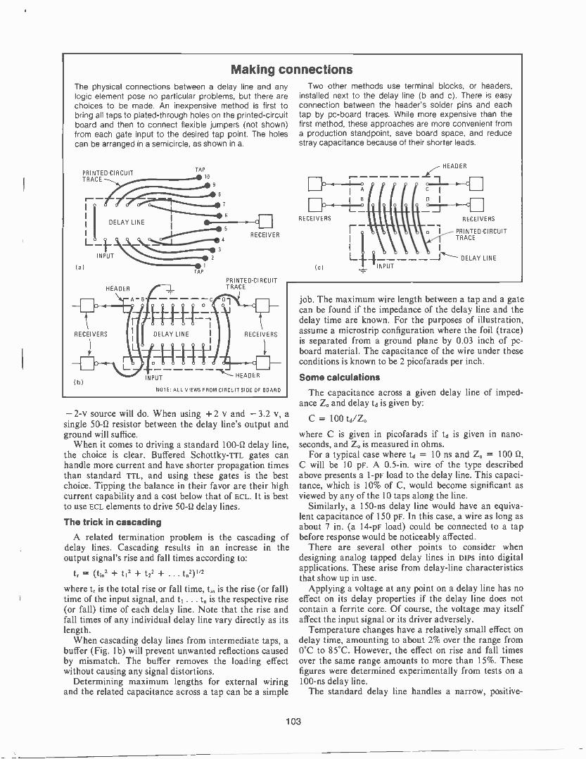
Making connectionsThe physical connections between a delay line and anylogic element pose no particular problems, but there arechoices to be made. An inexpensive method is first tobring all taps to plated -through holes on the printed -circuitboard and then to connect flexible jumpers (not shown)from each gate input to the desired tap point. The holescan be arranged in a semicircle, as shown in a.
PRINTED -CIRCUITTAP
TRACE 10
(a)
.0091;c:.41
I DELAY LINE
f.INPUT 2
1
HEADER
RECEIVERS
(b)
TAP
DELAY LINE
th-f-1-4-1HEADER
4RECEIVER
PRINTED -CIRCUITTRACE
RECEIVERS
NOTE ALL VIEWS FROM CIRCUIT SIDE OF BOARD
Two other methods use terminal blocks, or headers,installed next to the delay line (b and c). There is easyconnection between the header's solder pins and eachtap by pc -board traces. While more expensive than thefirst method, these approaches are more convenient froma production standpoint, save board space, and reducestray capacitance because of their shorter leads.
HEADER
I A
CD-4=oD I
RECEIVERS
( c )
RECEIVERS
PRINTED -CIRCUITTRACE
L 4 - _ _ _ _ DELAY LINEINPUT
- 2-v source will do. When using + 2 v and - 3.2 v, asingle 50-12 resistor between the delay line's output andground will suffice.
When it comes to driving a standard 10042 delay line,the choice is clear. Buffered Schottky-rrL gates canhandle more current and have shorter propagation timesthan standard rri., and using these gates is the bestchoice. Tipping the balance in their favor are their highcurrent capability and a cost below that of ECL. It is bestto use ECL elements to drive 5042 delay lines.
The trick in cascading
A related termination problem is the cascading ofdelay lines. Cascading results in an increase in theoutput signal's rise and fall times according to:
tr = (tint t12 t22 t.2)1/2
where tr is the total rise or fall time, is the rise (or fall)time of the input signal, and t1 . to is the respective rise(or fall) time of each delay line. Note that the rise andfall times of any individual delay line vary directly as itslength.
When cascading delay lines from intermediate taps, abuffer (Fig. lb) will prevent unwanted reflections causedby mismatch. The buffer removes the loading effectwithout causing any signal distortions.
Determining maximum lengths for external wiringand the related capacitance across a tap can be a simple
job. The maximum wire length between a tap and a gatecan be found if the impedance of the delay line and thedelay time are known. For the purposes of illustration,assume a microstrip configuration where the foil (trace)is separated from a ground plane by 0.03 inch of pc -board material. The capacitance of the wire under theseconditions is known to be 2 picofarads per inch.
Some calculations
The capacitance across a given delay line of imped-ance Z. and delay td is given by:
C = 100 td/Z.
where C is given in picofarads if td is given in nano-seconds, and Z. is measured in ohms.
For a typical case where td = 10 ns and Z. = 100 S2,C will be 10 pF. A 0.5 -in. wire of the type describedabove presents a 1-pF load to the delay line. This capaci-tance, which is 10% of C, would become significant asviewed by any of the 10 taps along the line.
Similarly, a 150-ns delay line would have an equiva-lent capacitance of 150 pF. In this case, a wire as long asabout 7 in. (a 14-pF load) could be connected to a tapbefore response would be noticeably affected.
There are several other points to consider whendesigning analog tapped delay lines in DIPS into digitalapplications. These arise from delay -line characteristicsthat show up in use.
Applying a voltage at any point on a delay line has noeffect on its delay properties if the delay line does notcontain a ferrite core. Of course, the voltage may itselfaffect the input signal or its driver adversely.
Temperature changes have a relatively small effect ondelay time, amounting to about 2% over the range from0°C to 85°C. However, the effect on rise and fall timesover the same range amounts to more than 15%. Thesefigures were determined experimentally from tests on a100-ns delay line.
The standard delay line handles a narrow, positive -
103
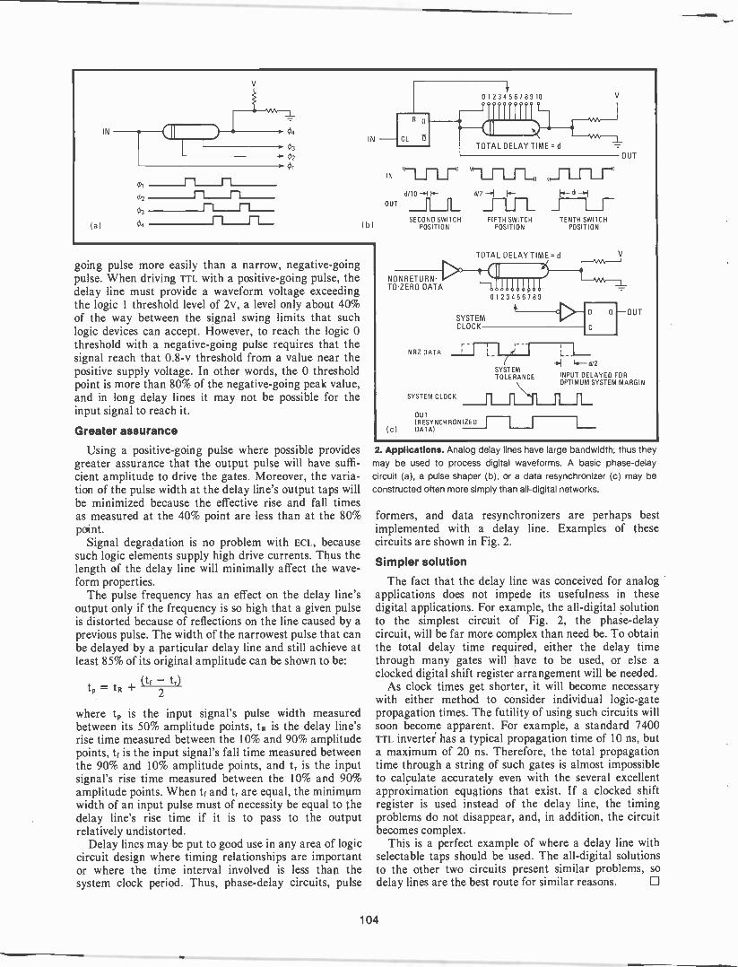
IN
(a)
951
02
03
04
IN
(b)
going pulse more easily than a narrow, negative -goingpulse. When driving TTL with a positive -going pulse, thedelay line must provide a waveform voltage exceedingthe logic 1 threshold level of 2v, a level only about 40%of the way between the signal swing limits that suchlogic devices can accept. However, to reach the logic 0threshold with a negative -going pulse requires that thesignal reach that 0.8-v threshold from a value near thepositive supply voltage. In other words, the 0 thresholdpoint is more than 80% of the negative -going peak value,and in long delay lines it may not be possible for theinput signal to reach it.
Greater assurance
Using a positive -going pulse where possible providesgreater assurance that the output pulse will have suffi-cient amplitude to drive the gates. Moreover, the varia-tion of the pulse width at the delay line's output taps willbe minimized because the effective rise and fall timesas measured at the 40% point are less than at the 80%point.
Signal degradation is no problem with Ect_., becausesuch logic elements supply high drive currents. Thus thelength of the delay line will minimally affect the wave-form properties.
The pulse frequency has an effect on the delay line'soutput only if the frequency is so high that a given pulseis distorted because of reflections on the line caused by aprevious pulse. The width of the narrowest pulse that canbe delayed by a particular delay line and still achieve atleast 85% of its original amplitude can be shown to be:
(tf - tr)t - tR +
2
where tp is the input signal's pulse width measuredbetween its 50% amplitude points, tR is the delay line'srise time measured between the 10% and 90% amplitudepoints, tr is the input signal's fall time measured betweenthe 90% and 10% amplitude points, and tr is the inputsignal's rise time measured between the 10% and 90%amplitude points. When tr and tr are equal, the minimtimwidth of an input pulse must of necessity be equal to thedelay line's rise time if it is to pass to the outputrelatively undistorted.
Delay lines may be put to good use in any area of logiccircuit design where timing relationships are importantor where the time interval involved is less than thesystem clock period. Thus, phase -delay circuits, pulse
O
CL 0
IN --Lriri
0 1 2 3 4 5 6 7 89 10
TOTAL DELAY TIME = d
V
d/10 14-
OUT 11
SECOND SWITCHPOSITION
NONRETURN-TO-ZERO
re>DATA
NRZ DATA
SYSTEM CLOCK
d/2 d
FIFTH SWITCH TENTH SWITCHPOSITION POSITION
TOTAL DELAY TIME = d
1(0d,111111
SYSTEMCLOCK
OUT(IESYNCHRONIZED
(c) DATA)
0 2 3 4 5 6 7 8 9
SYSTEMTOLERANCE
OUT
1.1 d/2
V
D -OUT
INPUT DELAYED FOROPTIMUM SYSTEM MARGIN
2. Applications. Analog delay lines have large bandwidth; thus theymay be used to process digital waveforms. A basic phase -delaycircuit (a), a pulse shaper (b), or a data resynchronizer (c) may beconstructed often more simply than all -digital networks.
formers, and data resynchronizers are perhaps bestimplemented with a delay line. Examples of thesecircuits are shown in Fig. 2.
Simpler solution
The fact that the delay line was conceived for analogapplications does not impede its usefulness in thesedigital applications. For example, the all -digital solutionto the simplest circuit of Fig. 2, the phase -delaycircuit, will be far more complex than need be. To obtainthe total delay time required, either the delay timethrough many gates will have to be used, or else aclocked digital shift register arrangement will be needed.
As clock times get shorter, it will become necessarywith either method to consider individual logic -gatepropagation times. The futility of using such circuits willsoon become apparent. For example, a standard 7400TTL inverter has a typical propagation time of 10 ns, buta maximum of 20 ns. Therefore, the total propagationtime through a string of such gates is almost impossibleto calculate accurately even with the several excellentapproximation equations that exist. If a clocked shiftregister is used instead of the delay line, the timingproblems do not disappear, and, in addition, the circuitbecomes complex.
This is a perfect example of where a delay line withselectable taps should be used. The all -digital solutionsto the other two circuits present similar problems, sodelay lines are the best route for similar reasons. LI
104
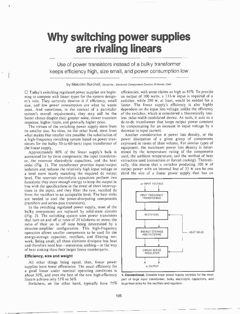
Why switching power suppliesare rivaling linears
Use of power transistors instead of a bulky transformerkeeps efficiency high, size small, and power consumption low
by Malcolm Burchall, Gould Inc., Electronic Components Division, El Monte, Calif
Today's switching regulated power supplies are begin-ning to compete with linear types for the system design-er's vote. They certainly deserve it if efficiency, smallsize, and low power consumption are what he wantsmost. And sometimes, in the context of a particularsystem's overall requirements, they may still be thebetter choice despite their greater noise, slower transientresponse, higher ripple, and generally higher price.
The virtues of the switching power supply stem fromits smaller size. Its vices, on the other hand, stem fromwhat makes that smaller size possible: the substitution ofa high -frequency switching system based on power tran-sistors for the bulky 50 -to -60 -hertz input transformer ofthe linear supply.
Approximately 80% of the linear supply's bulk isaccounted for by three components: the input transform-er, the reservoir electrolytic capacitors, and the heatsinks (Fig. 1). The transformer provides input/outputisolation and reduces the relatively high input voltage toa level more nearly matching the required dc outputlevel. The reservoir electrolytic capacitors perform twofunctions: they store enough energy to keep the output inline with the specifications in the event of short interrup-tions in the input, and they filter the raw, rectified dcfrom the rectifiers to an acceptable level. The heat sinksare needed to cool the power -dissipating components(rectifiers and series -pass transistors).
In the switching regulated power supply, most of thebulky components are replaced by solid-state circuits(Fig. 2). The switching system uses power transistorsthat turn on and off at rates of 20 kilohertz or more, theratio of their on to off time being determined by adetector -amplifier configuration. This high -frequencyoperation allows smaller components to be used for theenergy -storage capacitor, rectifiers, and filtering net-work. Being small, all these elements dissipate less heatand therefore need less-sometimes nothing-in the wayof heat sinking than their larger linear counterparts.
Efficiency, size and weight
All other things being equal, then, linear powersupplies have lower efficiencies. The usual efficiency fora good linear under nominal operating conditions isabout 50%, and even the best of the new high -efficiencylinears achieve only 53% to 56%.
Switchers, on the other hand, typically have 75%
efficiencies, with some claims as high as 85%. To providean output of 100 watts, a 133-w input is required of aswitcher, while 200 w, at least, would be needed for alinear. The linear supply's efficiency is also highlydependent on the input line voltage, unlike the efficiencyof the switcher, which is considered a theoretically loss -less pulse -width -modulated device. As such, it acts as adc -to -dc transformer that keeps output power constantby compensating for an increase in input voltage by adecrease in input current.
Another consideration is power loss density, or thepower dissipation of a given group of componentsexpressed in terms of their volume. For similar types ofequipment, the maximum power loss density is deter-mined by the temperature rating of the componentsused, the ambient temperature, and the method of heatextraction used (convection or forced cooling). Theoreti-cally, this means that a switcher producing 100 w ofoutput power with an internal loss of 33 w can be onethird the size of a linear power supply that has an
ac INPUT VOLTAGE
INPUT FREQUENCYTRANSFORMER
RECTIFIERS
ENERGY STORAGEAND FILTERING
LINEAR SERIESREGULATOR
dc OUTPUT
HEAT SINKS
1. Conventional. Sizeable linear power supply consists for the mostpart of large input transformer, bulky electrolytic capacitors, andlarge heat sinks for the rectifiers and regulator.
105
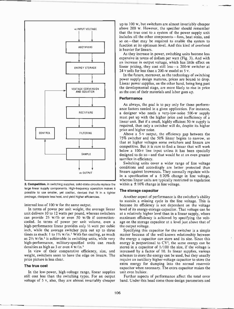
2. Competition. In switching supplies, solid-state circuits replace thelarge linear supply components. High -frequency operation makes itpossible to use smaller, yet costlier, devices that fit in a tighterpackage, dissipate less heat, and yield higher efficiencies.
internal loss of 100 w for the same output.In terms of power per unit weight, the average linear
unit delivers 10 to 12 watts per pound, whereas switcherscan provide 25 w/lb or even 50 w/lb if convection -cooled. In terms of power per unit volume, even ahigh-performance linear provides only 1/2 watt per cubicinch, while the average switcher puts out up to threetimes as much: 1 to 11/2 w/in.3 With fan cooling, as muchas 21/2 w/in.' is achievable in switching units, while veryhigh-performance, military -specified units can reachdensities as high as 3 or even 4 w/in.3
In view of their comparative efficiency, size, andweight, switchers seem to have the edge on linears. Theprice picture is less clear.
The true cost
In the low -power, high -voltage range, linear suppliesstill cost less than the switching types. For an outputvoltage of 5 v, also, they are almost invariably cheaper
up to 100 w, but switchers are almost invariably cheaperabove 200 w. However, the specifier should rememberthat the true cost to a system of the power supply unitincludes all the other components-fans, heat sinks, andso on-that may be required to enable the system tofunction at its optimum level. And this kind of overheadis heavier for linears.
As they increase in power, switching units become lessexpensive in terms of dollars per watt (Fig. 3). And withan increase in output voltage, which has little effect onlinear pricing, they cost still less-a 200-w switcher at24 v sells for less than a 200-w model at 5 v.
In the future, moreover, as the technology of switchingpower supply design matures, prices are bound to drop.Linear power supplies, on the other hand, being long pastthe developmental stage, are more likely to rise in priceas the cost of their materials and labor goes up.
Performance
As always, the goal is to pay only for those perform-ance factors needed in a given application. For instance,a designer who needs a very -low -noise 500-w supplymust put up with the higher price and inefficiency of alinear unit. But if a small, highly efficient 50-w supply isrequired, then only a switcher will do, despite its higherprice and higher noise.
Above a 5-v output, the efficiency gap between the75% switcher and the 50% linear begins to narrow, sothat at higher voltages some switchers and linears arecompetitive. But it is rare to find a linear that will workbelow a 100-v line input unless it has been speciallydesigned to do so-and that would be at an even greatersacrifice in efficiency.
Switching units cover a wider range of line voltageconditions and accordingly are better protected thanlinears against brownouts. They normally regulate with-in a specification of a ± 20% change in line voltage,whereas linear units are typically restricted to regulationwithin a ± 10% change in line voltage.
The storage capacitor
Another aspect of performance is the switcher's abilityto sustain, a missing cycle in the line voltage. This isbecause its efficiency is not dependent on the voltagelevel of its energy -storage capacitor. That voltage can beat a relatively higher level than in a linear supply, wheremaximum efficiency is achieved by specifying the volt-age on the storage capacitor at a level just above that ofthe output voltage.
Specifying this capacitor for the switcher is a simplematter because of the well-known relationship betweenthe energy a capacitor can store and its size. Since thisenergy is proportional to CV2, the same energy can bestored in a capacitor of 1/100 the size, if the voltage isincreased by a factor of 10. In linear supplies, variousschemes to store the energy can be used, but they usuallyrequire an auxiliary higher -voltage capacitor to store theextra energy for dumping into the normal reservoircapacitor when necessary. The extra capacitor makes theunit even bulkier.
Further aspects of performance affect the total errorband. Under this head come those design parameters and
106

10
3
2
0.8
0.6 -0.5
10
mmnosil emomminNOMMUMMU
MENEM MEN11111Ening 11111111111
11111111.11111111mimmommonewn.;:ImmiNimENNINEMEMEmniimmanwhogimi
IIIIMMEMENIIM11111111111U11111111
20 40 60 100 2 0 400 600 1,000
OUTPUT (WI
3. What price power? The larger their power output, the lessexpensive switching power supplies become in terms of their cost per
watt. The graph assumes 100 -quantity price and middle-of-the-roadspecifications for fully encased switching units.
the component ratings that between them set the toler-ance level of the supply's output -voltage within a plusand minus band.
Transient response, ripple, temperature stability,setting capability, load regulation, and line regulation,all contribute to the total error band and are usefulcriteria for choosing between linear power supplies andswitching power supplies.
In recovering from a momentary transient, switchingunits are on the order of 10 to 20 times slower thanlinears. A linear recovers in tens of microseconds, whileit takes a switcher hundreds and sometimes even thou-sands of microseconds to recover. For rates of change ofload current slower than 0.1 ampere per microsecond,transient amplitude deviations become detrimental forthe switcher, producing deviations on the order of 1% to2% per 10% of load change, whereas linears producenegligible deviations because of their faster responsetime. On the other hand, for very fast rates of change ofload current, in excess of 1 Aims, the output inductanceof the power supply becomes the limiting factor, andhere switchers can actually be better than linears. Inthese circumstances, the length of the power leads to theload and local decoupling at the load normally controlthe transient voltages seen by the load.
It is to be noted, though, that in digital systems,typically one logic circuit turns on as another turns off,so that the average load remains fairly even. The tran-sients caused by these relatively minor load variationsare small in amplitude and so of little consequence inpower supply choice.
The switching functions within a switching powersupply create an inherent ripple that is normally worsethan in linears. That has always been the switcher's flaw.However, the ripple has a limited effect on power supplychoice, since it is usually buried in the total system noise.Most digital circuits can tolerate a total error band of atleast ±5%, which compares favorably with the ± 0.5%ripple commonly observed in switchers. The usual indus-try standard for switching power supplies is 50 my or 1%peak to peak.
As far as temperature stability and load- and line -regulation and setting -capability tolerances are con-cerned, these are functions of component quality and of
TRADEOFFS
Parameter
IN CHOOSINGLINEAR REGULATED
Switchingpower
supplies
A SWITCHINGPOWER
Linearpower
supplies
ORSUPPLY
Remarks
Volume/watt excellent poor approximately 3:1 switcher-to-linear advantage
Weight/watt excellent poor approximately 3.1 switcher-to-linear advantage
Power levels unlimitedin practice
not normallyabove 500 W
switcher has less waste heat:higher power is possible
Noise acceptable excellent linear not always better -care in design required
Versatility excellent good switcher has wide line -voltage tolerance andbrown -out protection
Error band acceptableto good
acceptableto excellent
depends on the amount ofripple noise and transientresponse
Reliability acceptableto excellent
acceptableto excellent
depends on quality ofdesign and components
the design techniques used in both the switcher andlinear supplies. No basis for comparison between switch-ers and linears exists here.
The same can also be said of current limiting. Bothlinears and switchers contain current -limiting circuitryand are fairly well protected against that hazard.
However, the two kinds of supply differ in the waythey fail in response to excessive output -voltage varia-tions. In this situation, linears normally have a cata-strophic effect on their loads because they end up in anovervoltage condition. Still, it is easy enough to design anovervoltage crowbar circuit for them. This circuitconsists of a threshold device that senses when an outputovervoltage occurs and at once connects a high -current,fast -acting circuit, or crowbar (usually a siliconcontrolled rectifier) across the output terminals. Switch-ers, on the other hand, normally tend to fail downwardsto an undervoltage condition. For those cases where theymay end up in an overvoltage condition, a protectivecircuit for shutting them down can be provided thatoperates at much smaller currents than in linears.
To sum up, then, in terms of the total -error band, thechoice between a linear and a switcher is a hard one,even with the latter displaying the worse ripple.
Switch -on surges
There is a tendency to think that line -current switch -on surges created by switchers are much worse thanthose created by linears. Actually, the switch -on surge ina switcher is usually confined to the first one or twocharging current pulses, whereas in a linear, the switch -on surge current required to demagnetize the transform-er core can last for as many as 20 pulses if the 50 -60 -Hztransformer is switched off and switched on again at theworst possible phase relationship. With the large switch-ers, soft -start circuits are provided that spread thecurrent over several smaller pulses rather than the justone or two charging pulses. This makes the switcherseven more attractive for tackling the surge problem.
Finally, for both the linear and the switcher, the solecriterion as far as radio -frequency- and electromagnetic -interference tolerances are concerned is whether eithersupply can meet typical international specifications suchas the VDE 0875 EMI and RFI Specifications. CI
107

Standard symbols let designers grasplogic operation quickly and easily
ANSI Y32.14 specifies set of symbols forclearly depicting logic, from gates to systems
by Bill King, Hewlett-Packard Co., Santa Clara (Calif.) Division
0 The more complex integrated circuits become, thegreater the detail in which designers and techniciansneed to understand their workings. To give them thatinformation at a glance, manufacturers must depict thelogic operation of their chips clearly and concisely.
In 1973, therefore, the American National StandardsInstitute approved and published ANSI Y32.14, whichset the logic -symbol specifications for most devices-notably gates, flip-flops, and counters-and for systemscontaining them. But few users are familiar with thestandard, because so far it has been adopted by only twomanufacturers-by Hewlett-Packard Co. and, to someextent, by Texas Instruments Inc. Nonetheless, sinceANSI does set standards for 1c makers, its symbolism islikely to become widely accepted.
Symbol
TABLE 1: BASIC
Function
LOGIC ELEMENTS
Description
1>--- amplifier
The output will be active onlywhen the input is active (canbe used with polarity or logicindicator at input or output tosignify inversion).
Or ANDoutput will assume its
indicated active state onlywhen all its inputs assumetheir indicated active levels.
The
f
&
Or OR
The output will assume itsindicated active state onlywhen any of its inputs assumetheir indicated active levels.
311)
> 1
Or
BOexclusive -OR
The output will assume itsindicated active level if, andonly if, only one of the inputsassumes its indicated activelevel.= 1
wired -AND
This is a connection of outputsof two or more elements thatare joined together to achievethe effect of an AND function.0--
wired -ORThis is a connection of outputsof two or more elements thatare joined together to achievethe effect of an OR function.1)---
ANSI Y32.14 specifies: Definitions for the basic logic elements. Logic symbols, which show the defining shapes corre-sponding to the logic function performed. Qualifiers, which consist of letters, numbers, or arrowsplaced inside the logic -device symbol to indicate its logicfunction or special properties. Indicators, which show primarily if the input andoutput are active high or low. Dependency notation, which defines the logic -staterelationship between the inputs required to activate thedevice. Control and contiguous blocks, which integrate withgates, flip-flops, and other elements to form shift regis-ters, counters, and other commonly used devices.
TABLE 2: SELECTED
Symbol
QUALIFIER DESIGNATIONS
Description
Bilateral switch: a binary -controlled circuitthat acts as an on -off switch to analog orbinary signals flowing in both directions.
..__...
Logic threshold: output will assume itsactive state if m or more inputs are active.
rn
----m and only m: output will be active whenm and only m inputs are active (for example,exclusive -OR).
in
Majority function: output will be active onlyif more than half the inputs are active.
>0/2
Odd function: output is active only if an oddnumber of inputs are active.
mod
Even function: output is active only if an evennumber of inputs are active.
00
Signal -level converter: input levels are differentfrom output levels.
x/y
108

(a)
(b)
y = LOW, x = ACTIVEy = HIGH, x = INACTIVE
x = ACTIVE, y = LOWx= INACTIVE, y = HIGH
y= HIGH, x = ACTIVEy = LOW, x = INACTIVE
x= ACTIVE, y = HIGHx = INACTIVE, y = LOW
1. Polarity convention. Indicator symbol (top) signifies that corre-sponding inputs or outputs are active low (a), thereby characterizingCircuit operation without use of labeled outputs. The absence of thesymbol (b) indicates inputs and outputs are active high.
Table 1 gives the definitions of the basic elements-the amplifier, AND, OR, exclusive-oR, wired -AND, andwired-oR circuits-and their logic symbols. Note thatthe AND, OR, and exclusive-oR can be shown by theirassigned shape or by a rectangle, since the presence of anidentifying symbol within those elements specifies thedevice function. The inverting function for theseelements (that is, inverter, NAND, or NOR) is indicated byplacing the negation symbol (a small circle) at thecorresponding output ports of the devices-the samesymbol used currently. In addition to specifying thefunction of a logic element, qualifier symbols are usedfor classifying logic blocks. Table 2 shows the symbols
Flip-flop Originau symbols
TABLE 3: FLIP-FLOP
Previous standardMIL -STD -806B
SYMBOLISM
ANSI Y32.14Control designations description for flip-flop
R -SD
D
I R S Q aP
S Q
Q
C
F FR
S
I I
I h
h I
h h
n.c. n.c.
h I
I h
undetermined
S
R FF -RI
TD
p
Toggling occurs with everyclock pulse.
0
T
a
FF
T
-T
FF
DD Data output follows data input;
input is gated by C.
P
0 Q
CLK
Q
C
CFF
DG
R
s
D -= FF s' "-.
J -KD
D
J K Q bP
J 0
K Q
C
FF
K
R
S
1
."-
I I
I h
h I
h h
n.c. n.c.I h
h I
toggles
--FFK
"--
J -K(gated) H D
I- D
J and K inputs are gated by C.
P
J Q
CLK
C
JG F F
G
Ke
Rs
J
....KFF "--....
J -K(master-slave)
Outputs are dependent on thenegative -going edge of the clock.
jG FFG
Kr,
R
S
`-
...-.."
n.c. = no change
109
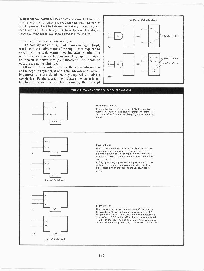
2. Dependency notation. Block -diagram equivalent of two -inputAND gate (a), which drives one-shot, provides quick overview ofcircuit operation. Identifier indicates dependency between inputs aand b, showing data on b is gated in by a. Approach to coding upthree -input AND gate follows logical extension of method (b).
for some of the most widely used ones.The polarity indicator symbol, shown in Fig. 1 (top),
establishes the active states of the input leads required toswitch on the logic element or indicates whether theoutput leads are active high or low. Any input or outputso labeled is active low (a). Otherwise, the inputs oroutputs are active high (b).
Although this symbol provides the same informationas the negation symbol, it offers the advantage of visual-ly representing the signal polarity required to activatethe device. Furthermore, it eliminates the inconsistentlabeling of logic devices. For example, the inverted
TABLE 4 COMMON CONTROL -BLOCK DEFINITIONS
Shift register block
This symbol is used with an array of flip-flop symbols toform a shift register. The data will shift to the right (- .)or to the left (4---) on the positive -going edge of the inputsignal.
Counter block
This symbol is used with an array of flip-flops or othercircuits serving as a binary or decade counter. In (a),the positive -going edge of an input to either the +m or-m input causes the counter to count upward or down-ward m times.In (b), a positive -going edge of an input to the ±m portwill cause the counter to increment or decrement mtimes depending on the input to the up -down controlIL/D).
(not ANSI -defined)
(a)
G1
G2
G3
SEL
SO
S1
(b) SEL r -(not ANSI -defined)
Selector block
This control block is used with an array of OR symbolsto provide for the gating lines (a) or selection lines (b(.
The gating lines have an AND relation with the respectiveinput of each OR function: G1 with the inputs numbered1, G2 with the inputs numbered 2, etc. The selection linesenable the input designated 0, 1, n of each OR function.
110

TABLE 5- COMMON DEVICE BLOCKS
4 -bit universal shift registerThis shift register has four parallel data inputs (Dc)and two synchronous serial data inputs (J, K). Thecontrol block contains those enable lines that willselect the way data is loaded into the register. Dataentry into the D flip-flops is dependent on C andG2 (Dc.2). A high input at C and a high at G2 willenable a parallel load on the positive -going edgeof G2.A serial load into the J -K flip-flop is dependenton GI and G2 (J0,2 , K0121. When there is a lowinput at GI and a high input at G2, data is loadedserially and shifted one position to the right onthe positive -going edge of G2.The device resets when there is a high present atthe reset.
- +1
--b. -1= 9, +1
-'=" C1
R= 0, -1
710 CNTRI
D, ;11 -+1
Di j21 -+1
D1 ql -+10, rej -+1
+1
-1=15,+1
-Cr Cl =0, -I
-116 CNTRfDi 1,1
D1
0, r4F, -D, ;8; _
Presettable decade counterThe counter control block is used to show thecommon inputs to a presettable decade up -downcounter. The symbol "+m" means to count up bym and "-rn" means to count down by m. (Note: ifm = 1, it may be omttted.) The "=9, +1" symbol isthe carry output or the terminal count up whenthe count equals 9. The "=0, -1" symbol is theborrow output or the terminal count down whenthe count equals 0. Cl is the control input for theD flip-flops and R is the master reset. When Cl isenabled, it loads all four flip-flops (DO in parallel.The presence of the output delay indicator is usedto indicate that the D flip-flops are master -slave.Flip-flop weights are indicated in the parentheses.
The symbol "10 CNTR" indicates that the counteris modulus 10.
2
2
4 AO -A158GIG2
Z
1,A
4 1, A A
12 1, Aio
RAM
2, A
2, A
2, A
5
1
9
DO
D1
D2
D3
Random-access memory(without identical input/output pins)Address selection is determined by the 4 -bitaddress input codes in the upper left cornerof the control block. These address codesare weighted to correspond to the possibleaddress )A0 -A,5). GI and G2 are the read/write enable. A low on pin 2 will enable datato be read into the chip in the memory loca-tion addressed; a high on pin 3 will enablethe chip to output data from the particularmemory location addressed. The inputs onthe lower left corner of the symbol arelabeled 1, A. This indicates that the informa-tion will be stored in the memory locationaddressed. 2, A on the outputs indicates thatthe data will be written from the memorylocation when G2 is enabled.
Presettable binary counterSame as above except that the carry output isindicated with "=15, +1," indicating that theterminal count up occurs when the count equals15. The symbol "16 CNTR" indicates that thecounter is modulus 16.
1
248163264128256512
Fl
AO - A1,023
ROM(threestate)
A,1 DO
A,1 DI
A,1 D2
A, 1 03
A,1 D4
A,1 D5
A, 1 D6
A, 1 D7
Read-only memoryThis is a read-only memory with 1,024addresses. Address selection is determinedby the 10 -bit address input in the upperleft corner of the control block.F1 is the three -state enable line. A highsignal on this line will enable the outputs.A, 1 on the outputs indicates the depen-dency on the three -state enable and thememory location addressed.
output of a flip-flop is normally designated .$5, and theinverted R and S inputs have negation symbols at theirports, rather than being labeled IT and g. These ports willnow be labeled Q, R, and S with appropriate polarityindicators. This change can be seen in Table 3, whichshows the development of flip-flop symbolism.
Block formBy providing for dependency symbols and one -block
devices, ANSI Y32.14 makes it easier for system design-ers to understand the operation of large circuits. So-called control blocks, which group the common controlinputs, can be joined to contiguous blocks, which depictthe remainder of the circuit (an array of gates, flip-flops,etc.). A combination of control and contiguous blocksforms a device block.
Figure 2 shows the application of dependency symbols.Dependency is indicated by subscripts, prefixes, orsuffixes. For example, in the case of DI, the 1 indicates alogic connection between the input, D, and a control lineassigned the numeral 1. In prefix form, the notationbecomes 1D; in suffix form, D 1.
In the simple example of Fig. 2a, a two -input AND gate
drives a one-shot multivibrator. The equivalent depen-dency for the gate is shown to the right. G1 is an input,through which data on line b is gated into the device.The 1 identifies the existence of the relationship betweenlines a and b, with the letter G defining the type ofrelationship (AND -gate dependency). The appropriateletter identifies other relationships: A (address), C (con-trol), F (free, or three -state), or V (oR-gate).
Figure 2b, an extension of Fig. 2a, shows how a circuithaving a three -input AND gate is coded. GI and G2 arethe gating inputs for data on line c, as indicated by the1,2 of the input 1,2 X.
Symbol buildupANSI'S recommended control blocks include a shift
register, a counter, and a selector, all of which are shownin Table 4. The lower figures of the counter block and ofthe selector block are not part of ANSI's standard, butthey have appeared occasionally in the literature and soare included for reference.
When these control blocks are united with contiguousblocks, such as flip-flops, then entire devices can be built.Several are illustrated in Table 5.
111
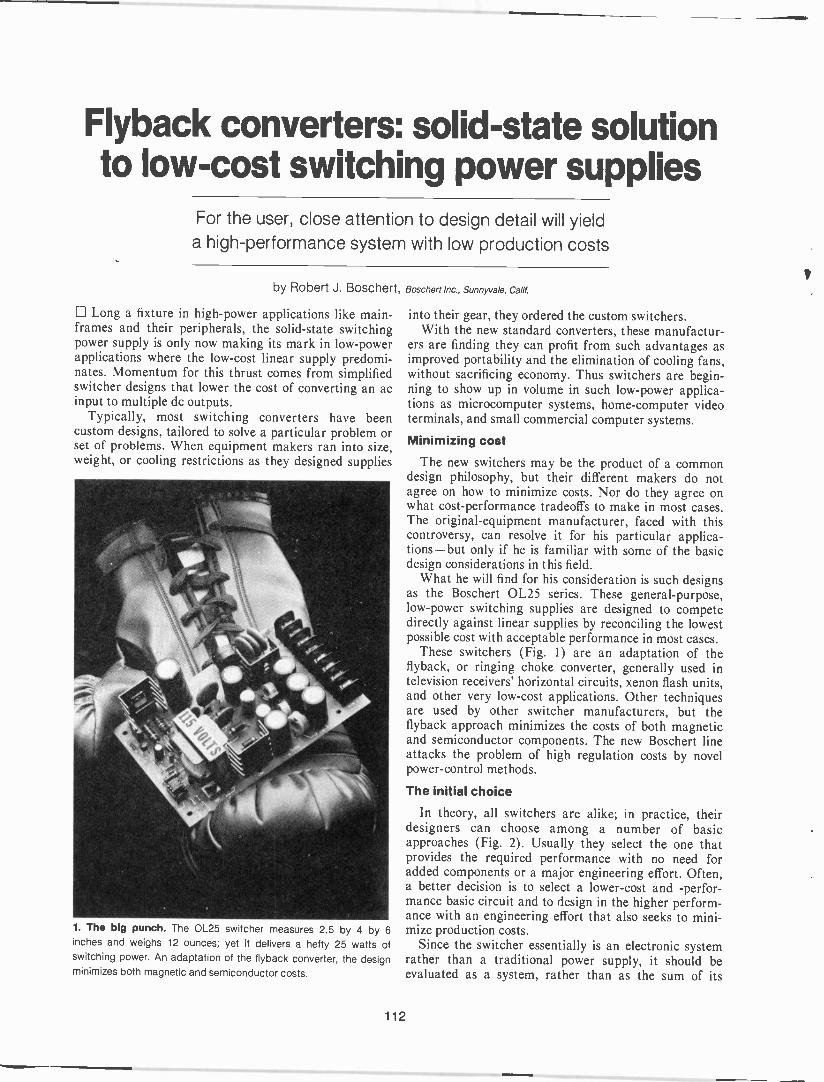
Flyback converters: solid-state solutionto low-cost switching power supplies
For the user, close attention to design detail will yielda high-performance system with low production costs
by Robert J. Boschert,
Long a fixture in high -power applications like main-frames and their peripherals, the solid-state switchingpower supply is only now making its mark in low -powerapplications where the low-cost linear supply predomi-nates. Momentum for this thrust comes from simplifiedswitcher designs that lower the cost of converting an acinput to multiple dc outputs.
Typically, most switching converters have beencustom designs, tailored to solve a particular problem orset of problems. When equipment makers ran into size,weight, or cooling restrictions as they designed supplies
1. The big punch. The OL25 switcher measures 2.5 by 4 by 6inches and weighs 12 ounces; yet it delivers a hefty 25 watts ofswitching power. An adaptation of the flyback converter, the designminimizes both magnetic and semiconductor costs.
Boschert Inc., Sunnyvale, Calif.
into their gear, they ordered the custom switchers.With the new standard converters, these manufactur-
ers are finding they can profit from such advantages asimproved portability and the elimination of cooling fans,without sacrificing economy. Thus switchers are begin-ning to show up in volume in such low -power applica-tions as microcomputer systems, home -computer videoterminals, and small commercial computer systems.
Minimizing cost
The new switchers may be the product of a commondesign philosophy, but their different makers do notagree on how to minimize costs. Nor do they agree onwhat cost -performance tradeoffs to make in most cases.The original -equipment manufacturer, faced with thiscontroversy, can resolve it for his particular applica-tions-but only if he is familiar with some of the basicdesign considerations in this field.
What he will find for his consideration is such designsas the Boschert OL25 series. These general-purpose,low -power switching supplies are designed to competedirectly against linear supplies by reconciling the lowestpossible cost with acceptable performance in most cases.
These switchers (Fig. 1) are an adaptation of theflyback, or ringing choke converter, generally used intelevision receivers' horizontal circuits, xenon flash units,and other very low-cost applications. Other techniquesare used by other switcher manufacturers, but theflyback approach minimizes the costs of both magneticand semiconductor components. The new Boschert lineattacks the problem of high regulation costs by novelpower -control methods.
The initial choice
In theory, all switchers are alike; in practice, theirdesigners can choose among a number of basicapproaches (Fig. 2). Usually they select the one thatprovides the required performance with no need foradded components or a major engineering effort. Often,a better decision is to select a lower -cost and -perfor-mance basic circuit and to design in the higher perform-ance with an engineering effort that also seeks to mini-mize production costs.
Since the switcher essentially is an electronic systemrather than a traditional power supply, it should beevaluated as a system, rather than as the sum of its
112
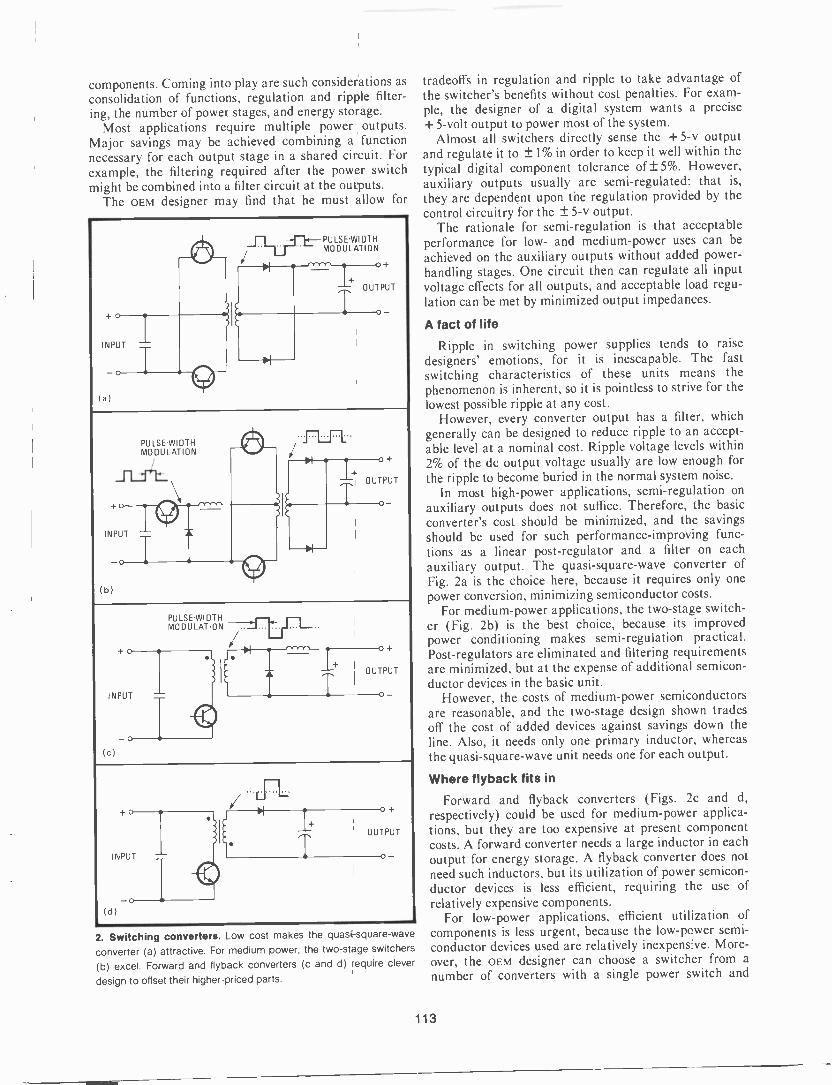
components. Coming into play are such considerations asconsolidation of functions, regulation and ripple filter-ing, the number of power stages, and energy storage.
Most applications require multiple power outputs.Major savings may be achieved combining a functionnecessary for each output stage in a shared circuit. Forexample, the filtering required after the power switchmight be combined into a filter circuit at the outputs.
The OEM designer may find that he must allow for
PULSE WIDTHel /111.07t.-MODULATIONi +
+OUTPUT
+
INPUT
I
I
- .
(a)
IIP4.1)
PULSEMODULATION
-WIDTH ip ... +
-11-11h.
1114
OUTPUT
+INPUT
a
(b)
PULSE WIDTHMODULATION .. .../ ... ... ..
-.---0++
INPUT
j; -3S-.-"-I
--- +OUTPUT
T _o
(c)
4.
INPUT -L
+
0+
OUTPUT
(d)
.
2. Switching converters. Low cost makes the quasi -square -waveconverter (a) attractive. For medium power, the two -stage switchers(b) excel. Forward and flyback converters (c and d) require cleverdesign to offset their higher -priced parts.
tradeoffs in regulation and ripple to take advantage ofthe switcher's benefits without cost penalties. For exam-ple, the designer of a digital system wants a precise+ 5 -volt output to power most of the system.
Almost all switchers directly sense the +5-v outputand regulate it to ± 1% in order to keep it well within thetypical digital component tolerance of ± 5%. However,auxiliary outputs usually are semi -regulated: that is,
they are dependent upon the regulation provided by thecontrol circuitry for the ± 5-v output.
The rationale for semi -regulation is that acceptableperformance for low- and medium -power uses can beachieved on the auxiliary outputs without added power -handling stages. One circuit then can regulate all inputvoltage effects for all outputs, and acceptable load regu-lation can be met by minimized output impedances.
A fact of lifeRipple in switching power supplies tends to raise
designers' emotions, for it is inescapable. The fastswitching characteristics of these units means thephenomenon is inherent, so it is pointless to strive for thelowest possible ripple at any cost.
However, every converter output has a filter, whichgenerally can be designed to reduce ripple to an accept-able level at a nominal cost. Ripple voltage levels within2% of the dc output voltage usually are low enough forthe ripple to become buried in the normal system noise.
In most high -power applications, semi -regulation onauxiliary outputs does not suffice. Therefore, the basicconverter's cost should be minimized, and the savingsshould be used for such performance -improving func-tions as a linear post -regulator and a filter on eachauxiliary output. The quasi -square -wave converter ofFig. 2a is the choice here, because it requires only onepower conversion, minimizing semiconductor costs.
For medium -power applications, the two -stage switch-er (Fig. 2b) is the best choice, because its improvedpower conditioning makes semi -regulation practical.Post -regulators are eliminated and filtering requirementsare minimized, but at the expense of additional semicon-ductor devices in the basic unit.
However, the costs of medium -power semiconductorsare reasonable, and the two -stage design shown tradesoff the cost of added devices against savings down theline. Also, it needs only one primary inductor, whereasthe quasi -square -wave unit needs one for each output.
Where flyback fits in
Forward and flyback converters (Figs. 2c and d,respectively) could be used for medium -power applica-tions, but they are too expensive at present componentcosts. A forward converter needs a large inductor in eachoutput for energy storage. A flyback converter does notneed such inductors, but its utilization of power semicon-ductor devices is less efficient, requiring the use ofrelatively expensive components.
For low -power applications, efficient utilization ofcomponents is less urgent, because the low -power semi-conductor devices used are relatively inexpensive. More-over, the OEM designer can choose a switcher from anumber of converters with a single power switch and
113

T
120 Vf MS ac
X Di63T
63T
C4
I I-RB 02
03
31
D4
5T
05
4T
8µH
1+
2µH
1+
+12V
41
06
5T
81.4H
D7 8µH
+5 V
OPTICAL ISOLATORMCT2E TL430
A1
+5 V
5V
12 V
SILICONCONT-ROLLEDRECTIFIER
3. The OL25 power supply. A novel control circuit to adjust current flow during operation is governed by a feedback from the + 5-V outputthrough A, and A2 to transistors 0, and Q2. The ±5-V outputs are regulated; the ± 12-V are semi -regulated.
one output change.Forward converters have been preferred over flyback
switchers because of their relatively higher performance.However, a flyback -based power supply can offer equiv-alent performance to a forward unit if its designer plowsback part of the savings in magnetic and semiconductorcosts into design improvements. The savings in outputinductors more than offsets the slight increase in trans-former complexity needed to combine the isolation andstorage functions.
Low-cost energyYet this more complex double -duty transformer
contributes heavily to the flyback converter's majoradvantage: lower -cost energy storage. Often overlookedas so fundamental a fact of switcher design, energystorage represents a large chunk of total system costs, aswell as being a key to the unit's efficiency.
Energy is stored when the power -switching transistorturns on and is delivered to the load when the transistorturns off. Switch -control regulation thus replaces thehighly inefficient energy -dissipation techniques used toregulate linear power supplies.
However, most switchers must store their energy inexpensive magnetic components. By storing energy in theisolation transformer, the flyback converter eliminatesthis component expense. Moreover, it needs the fewestcomponents for each basic power -handling function. Infact, one component suffices for each function, because
the flyback converter is a single -ended circuit.As the Boschert OL25 series shows, the result can be a
versatile design (Fig. 3) that provides 25 watts maxi-mum in four continuous outputs over worst -case line-
power conditions. The basic model has ± 5-v regulatedoutputs and ± 12-v semi -regulated outputs. A modulardesign approach allows outputs to be tailored for option-al voltages throughout a ±40-v range.
The main challenge in flyback design is to minimizethe cost of the control circuitry. In general, controllingthe output power is achieved by a blocking oscillatorpower stage that changes state whenever total positivefeedback gain from the switching section through thetransformer exceeds unity. The blocking oscillator thenusually delivers a fixed amount of power.
Controlling the power
The OL25 operates as a blocking oscillator under thefollowing control law: output is linearly proportional tocurrent flowing in the primary circuit at the time transis-tor Q, in Fig. 3 turns off. The simplifying assumption ismade that output power is independent of input linevoltage and operating frequency, so far as the controlloop is concerned. Then the control -loop model for thepower stage is simply a current source driving the outputcapacitances.
To adjust power flow during operation, the OL25implements a novel control circuit. The new techniqueprovides excellent regulation resulting in significant
114
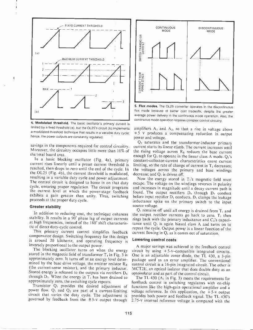
4. Modulated threshold. The basic oscillator's primary current islimited by a fixed threshold (a), but the OL25's circuit (b) implementsa modulated threshold technique that results in a variable duty cycle;hence, the power outputs are constantly regulated.
savings in the components required for control circuitry.Moreover, the circuitry occupies little more than 10% ofthe total board area.
In a basic blocking oscillator (Fig. 4a), primarycurrent rises linearly until a preset current threshold isreached, then drops to zero until the end of the cycle. Inthe OL25 (Fig. 4b), the current threshold is modulated,resulting in a variable duty cycle and power adjustment.The control circuit is designed to home in on that dutycycle, ensuring proper regulation. The circuit programsthe current level at which the power -stage feedbackexhibits a gain greater than unity. Thus, switchingproceeds at the proper duty cycle.
Greater stability
In addition to reducing cost, the technique enhancesstability. It results in a 90° phase lag of output currentsat high frequencies, instead of the 180° shift characteris-tic of direct duty -cycle control.
This primary current control simplifies feedbackcompensator design. Switching frequency for this designis around 20 kilohertz, and operating frequency isinversely proportional to the output power.
The blocking oscillator turns on when the energystored in the magnetic field of transformer Ty in Fig. 3 isapproximately zero. It turns off at an energy level deter-mined by the base drive voltage, the emitter resistor RE(the current -sense resistor), and the primary inductor.Stored energy is released to the outputs via rectifiers D4through D7. When the energy in T1 has been drained toapproximately zero, the switching cycle repeats.
Transistor Q1 provides the desired adjustment ofpower flow. Q1 and Q2 are part of a current -limitingcircuit that varies the duty cycle. The adjustment isgoverned by feedback from the ± 5-v output through
cc0
7.7)
¢xzzawI- CC
OCDCC <
U,2 ccw
0CJ
CONTINUOUSMODE
/,11=6.
DISCONTINUOUSMODE
5. Flux modes. The OL25 converter operates in the discontinuousflux mode because of better cost tradeoffs, despite the greateraverage power delivery in the continuous mode operation. Also, thecontinuous mode operation requires complex control circuitry.
amplifiers AI and Az, so that a rise in voltage above+5 v produces a compensating reduction in outputpower and voltage.
Q1 saturates and the transformer -inductor primarycurrent starts its linear climb. The current increases untilthe rising voltage across RE reduces the base currentenough for Qi to operate in the linear class A mode. Qi'sconstant -collector -current characteristics cause currentlimiting, so the rate of change of current in T1 decreases;the voltages across the primary and base windingsdecrease; and Q1 is driven off.
Now the energy stored in TI's magnetic field mustescape. The voltage on the windings reverses in polarityand increases in magnitude until a decay current path isfound. The output rectifiers D4 through D7 conductbefore input rectifier DI conducts. DI clamps the leakageinductance spike on the primary switch to the inputsource voltage.
Q1 remains off until all energy is drained from T1 andthe output rectifier currents go back to zero. T1 thenrings back with the primary inductance and Cz's capaci-tance until Q1 is again biased class A and turns on torepeat the cycle. Output power is a linear function of thecurrent flowing in Q1 as it comes out of saturation.
Lowering control costs
A major savings was achieved in the feedback controlcircuit by using + 5-v-compatible integrated circuits.One is an adjustable zener diode, the TL 430, a 3 -pinpackage used as an error amplifier. The conventionalcontrol circuit is a 16 -pin integrated circuit. The other isMCT2E, an optical isolator that does double duty as anoptoisolator and as part of the control circuit.
The TL 430 (A1 in Fig. 3) meets the requirements forfeedback control in switching regulators with on -chipfunctions like the high -gain operational amplifier and avoltage reference. In this application, the + 5-v outputprovides both power and feedback signal. The TL 430's2.75-v internal reference voltage is compared with the
115
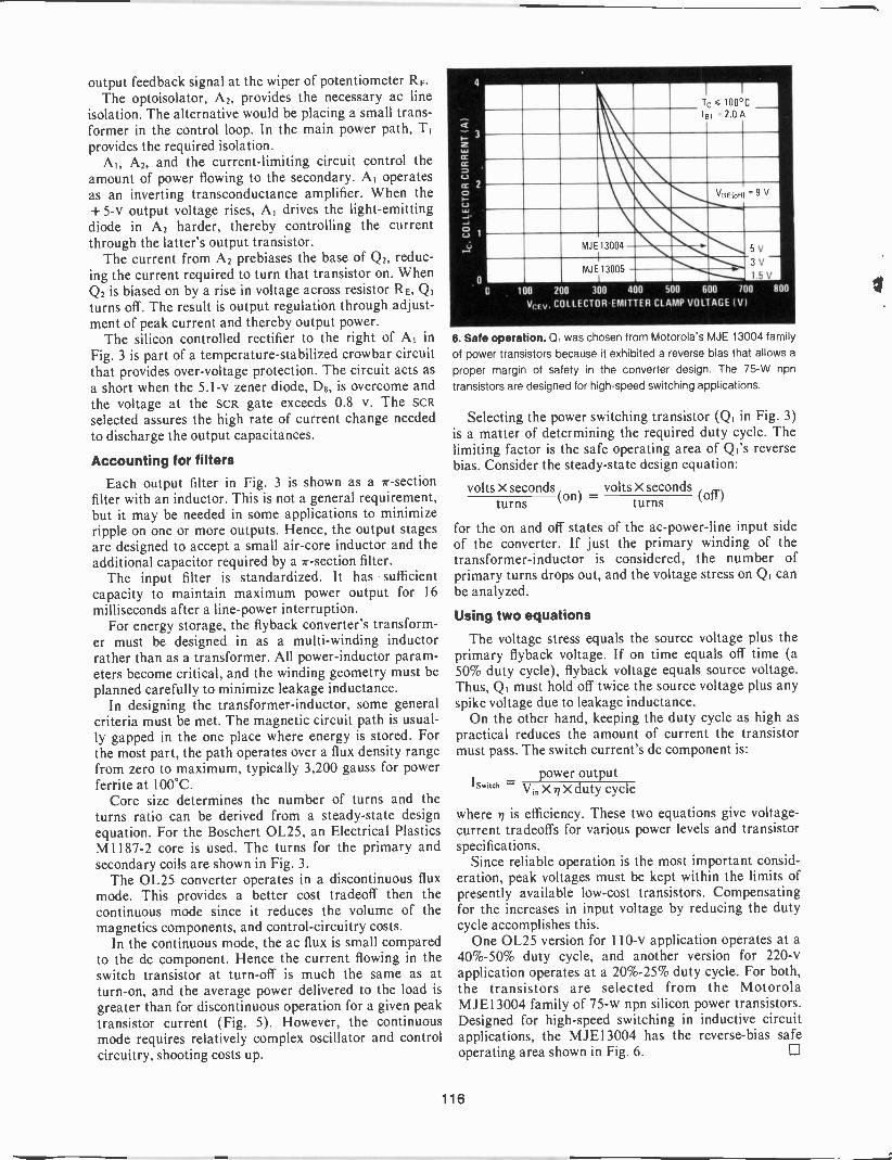
output feedback signal at the wiper of potentiometer R.The optoisolator, Az, provides the necessary ac line
isolation. The alternative would be placing a small trans-former in the control loop. In the main power path, T1provides the required isolation.
AI, Az, and the current -limiting circuit control theamount of power flowing to the secondary. AI operatesas an inverting transconductance amplifier. When the+5-v output voltage rises, AI drives the light -emittingdiode in A2 harder, thereby controlling the currentthrough the latter's output transistor.
The current from A2 prebiases the base of Qz, reduc-ing the current required to turn that transistor on. WhenQ2 is biased on by a rise in voltage across resistor RE, QIturns off. The result is output regulation through adjust-ment of peak current and thereby output power.
The silicon controlled rectifier to the right of AI inFig. 3 is part of a temperature -stabilized crowbar circuitthat provides over -voltage protection. The circuit acts asa short when the 5.1-v zener diode, D8, is overcome andthe voltage at the SCR gate exceeds 0.8 v. The SCR
selected assures the high rate of current change neededto discharge the output capacitances.
Accounting for filtersEach output filter in Fig. 3 is shown as a 7r -section
filter with an inductor. This is not a general requirement,but it may be needed in some applications to minimizeripple on one or more outputs. Hence, the output stagesare designed to accept a small air -core inductor and theadditional capacitor required by a 7r -section filter.
The input filter is standardized. It has sufficientcapacity to maintain maximum power output for 16
milliseconds after a line -power interruption.For energy storage, the flyback converter's transform-
er must be designed in as a multi -winding inductorrather than as a transformer. All power -inductor param-eters become critical, and the winding geometry must beplanned carefully to minimize leakage inductance.
In designing the transformer -inductor, some generalcriteria must be met. The magnetic circuit path is usual-ly gapped in the one place where energy is stored. Forthe most part, the path operates over a flux density rangefrom zero to maximum, typically 3,200 gauss for powerferrite at 100°C.
Core size determines the number of turns and theturns ratio can be derived from a steady-state designequation. For the Boschert OL25, an Electrical PlasticsM1187-2 core is used. The turns for the primary andsecondary coils are shown in Fig. 3.
The OL25 converter operates in a discontinuous fluxmode. This provides a better cost tradeoff then thecontinuous mode since it reduces the volume of themagnetics components, and control -circuitry costs.
In the continuous mode, the ac flux is small comparedto the dc component. Hence the current flowing in theswitch transistor at turn-off is much the same as atturn -on, and the average power delivered to the load isgreater than for discontinuous operation for a given peaktransistor current (Fig. 5). However, the continuousmode requires relatively complex oscillator and controlcircuitry, shooting costs up.
4
MJE13004
MJE 13005
100 200 300 400 500 600 700
VcFv, COLLECTOR -EMITTER CLAMP VOLTAGE (VI
800
6. Safe operation. 01 was chosen from Motorola's MJE 13004 familyof power transistors because it exhibited a reverse bias that allows aproper margin of safety in the converter design. The 75-W npntransistors are designed for high-speed switching applications.
Selecting the power switching transistor (Q, in Fig. 3)is a matter of determining the required duty cycle. Thelimiting factor is the safe operating area of QI's reversebias. Consider the steady-state design equation:
volts X seconds (on) - volts X secondsturns turns (off)
for the on and off states of the ac -power -line input sideof the converter. If just the primary winding of thetransformer -inductor is considered, the number ofprimary turns drops out, and the voltage stress on Qi canbe analyzed.
Using two equations
The voltage stress equals the source voltage plus theprimary flyback voltage. If on time equals off time (a50% duty cycle), flyback voltage equals source voltage.Thus, Q1 must hold off twice the source voltage plus anyspike voltage due to leakage inductance.
On the other hand, keeping the duty cycle as high aspractical reduces the amount of current the transistormust pass. The switch current's dc component is:
power outputIs"'" `h - v,,, x n x duty cycle
where n is efficiency. These two equations give voltage -current tradeoffs for various power levels and transistorspecifications.
Since reliable operation is the most important consid-eration, peak voltages must be kept within the limits ofpresently available low-cost transistors. Compensatingfor the increases in input voltage by reducing the dutycycle accomplishes this.
One OL25 version for 110-v application operates at a40%-50% duty cycle, and another version for 220-vapplication operates at a 20%-25% duty cycle. For both,the transistors are selected from the MotorolaMJE13004 family of 75-w npn silicon power transistors.Designed for high-speed switching in inductive circuitapplications, the MJE13004 has the reverse -bias safeoperating area shown in Fig. 6.
116

_

r
\

-1

d


0
I


14G07-099727-6