Embed Size (px)
Citation preview
FB
VIN VOUT
GND
VIN SW
RFB1
RFB2
EN
GNDVIDA
1
10
SON-10 3 mm x 3 mm
VIDB
VIDC
VIDS9
8
7
4
VDDIDAC_OUT
3
20 - 59.2 µA
LM10011
VCORE
2.97V to 5.5V
VIDInterface
RSET
SET6
MODE5
DC/DC
Product
Folder
Sample &Buy
Technical
Documents
Tools &
Software
Support &Community
LM10011SNVS822A –DECEMBER 2012–REVISED NOVEMBER 2014
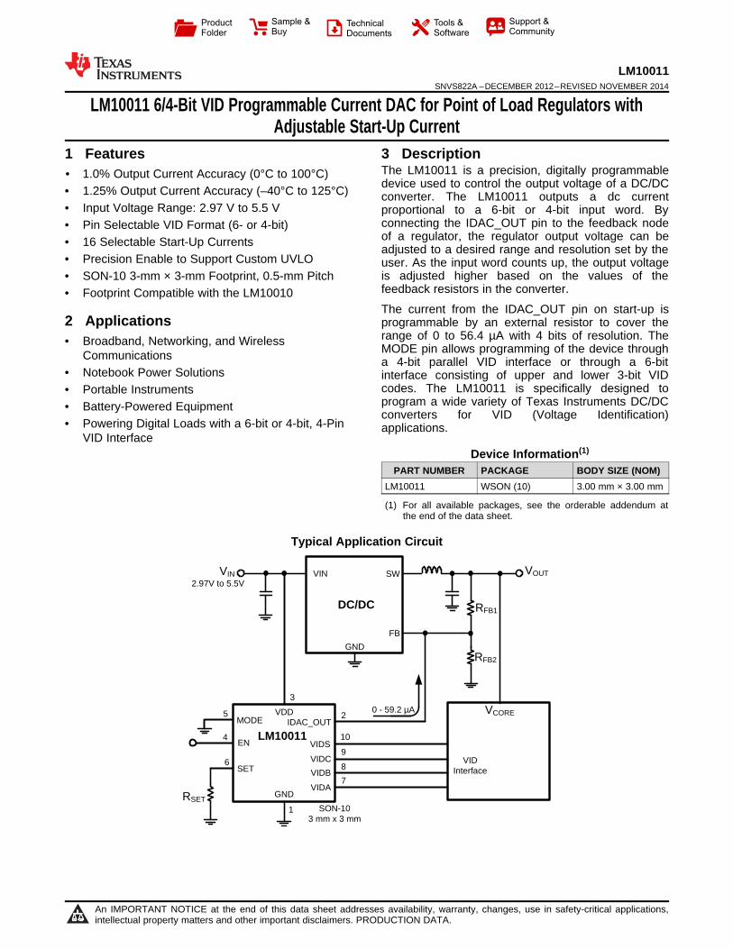
LM10011 6/4-Bit VID Programmable Current DAC for Point of Load Regulators withAdjustable Start-Up Current
1 Features 3 DescriptionThe LM10011 is a precision, digitally programmable
1• 1.0% Output Current Accuracy (0°C to 100°C)device used to control the output voltage of a DC/DC• 1.25% Output Current Accuracy (–40°C to 125°C) converter. The LM10011 outputs a dc current
• Input Voltage Range: 2.97 V to 5.5 V proportional to a 6-bit or 4-bit input word. Byconnecting the IDAC_OUT pin to the feedback node• Pin Selectable VID Format (6- or 4-bit)of a regulator, the regulator output voltage can be• 16 Selectable Start-Up Currents adjusted to a desired range and resolution set by the
• Precision Enable to Support Custom UVLO user. As the input word counts up, the output voltageis adjusted higher based on the values of the• SON-10 3-mm × 3-mm Footprint, 0.5-mm Pitchfeedback resistors in the converter.• Footprint Compatible with the LM10010The current from the IDAC_OUT pin on start-up is
2 Applications programmable by an external resistor to cover therange of 0 to 56.4 µA with 4 bits of resolution. The• Broadband, Networking, and Wireless MODE pin allows programming of the device throughCommunications a 4-bit parallel VID interface or through a 6-bit
• Notebook Power Solutions interface consisting of upper and lower 3-bit VIDcodes. The LM10011 is specifically designed to• Portable Instrumentsprogram a wide variety of Texas Instruments DC/DC• Battery-Powered Equipmentconverters for VID (Voltage Identification)
• Powering Digital Loads with a 6-bit or 4-bit, 4-Pin applications.VID Interface
Device Information(1)
PART NUMBER PACKAGE BODY SIZE (NOM)LM10011 WSON (10) 3.00 mm × 3.00 mm
(1) For all available packages, see the orderable addendum atthe end of the data sheet.
Typical Application Circuit
1
An IMPORTANT NOTICE at the end of this data sheet addresses availability, warranty, changes, use in safety-critical applications,intellectual property matters and other important disclaimers. PRODUCTION DATA.
LM10011SNVS822A –DECEMBER 2012–REVISED NOVEMBER 2014 www.ti.com
Table of Contents7.3 Feature Description................................................. 101 Features .................................................................. 17.4 Device Functional Modes........................................ 112 Applications ........................................................... 17.5 Programming........................................................... 113 Description ............................................................. 1
8 Application and Implementation ........................ 134 Revision History..................................................... 28.1 Application Information............................................ 135 Pin Configuration and Functions ......................... 38.2 Typical Application ................................................. 136 Specifications......................................................... 3
9 Power Supply Recommendations ...................... 166.1 Absolute Maximum Ratings ...................................... 310 Layout................................................................... 166.2 Handling Ratings....................................................... 4
10.1 Layout Guidelines ................................................. 166.3 Recommended Operating Conditions....................... 410.2 Layout Example .................................................... 176.4 Thermal Information .................................................. 4
11 Device and Documentation Support ................. 186.5 Electrical Characteristics........................................... 511.1 Trademarks ........................................................... 186.6 Typical Characteristics .............................................. 711.2 Electrostatic Discharge Caution............................ 187 Detailed Description .............................................. 911.3 Glossary ................................................................ 187.1 Overview ................................................................... 9
12 Mechanical, Packaging, and Orderable7.2 Functional Block Diagram ......................................... 9Information ........................................................... 18
4 Revision History
Changes from Original (December 2012) to Revision A Page
• Added Pin Configuration and Functions section, Handling Rating table, Feature Description section, DeviceFunctional Modes, Application and Implementation section, Power Supply Recommendations section, Layoutsection, Device and Documentation Support section, and Mechanical, Packaging, and Orderable Informationsection ................................................................................................................................................................................... 1
2 Submit Documentation Feedback Copyright © 2012–2014, Texas Instruments Incorporated
Product Folder Links: LM10011
VDD
IDAC_OUT
GND VIDS
VIDC
VIDB
VIDA
SET
1
3
2
5
4
10
9
8
7
6
DAP
EN
MODE
LM10011www.ti.com SNVS822A –DECEMBER 2012–REVISED NOVEMBER 2014
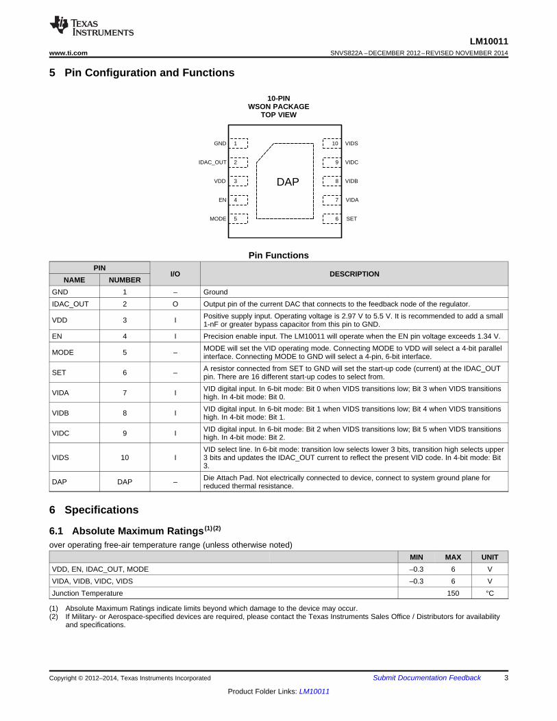
5 Pin Configuration and Functions
10-PINWSON PACKAGE
TOP VIEW
Pin FunctionsPIN
I/O DESCRIPTIONNAME NUMBER
GND 1 – GroundIDAC_OUT 2 O Output pin of the current DAC that connects to the feedback node of the regulator.
Positive supply input. Operating voltage is 2.97 V to 5.5 V. It is recommended to add a smallVDD 3 I 1-nF or greater bypass capacitor from this pin to GND.EN 4 I Precision enable input. The LM10011 will operate when the EN pin voltage exceeds 1.34 V.
MODE will set the VID operating mode. Connecting MODE to VDD will select a 4-bit parallelMODE 5 – interface. Connecting MODE to GND will select a 4-pin, 6-bit interface.A resistor connected from SET to GND will set the start-up code (current) at the IDAC_OUTSET 6 – pin. There are 16 different start-up codes to select from.VID digital input. In 6-bit mode: Bit 0 when VIDS transitions low; Bit 3 when VIDS transitionsVIDA 7 I high. In 4-bit mode: Bit 0.VID digital input. In 6-bit mode: Bit 1 when VIDS transitions low; Bit 4 when VIDS transitionsVIDB 8 I high. In 4-bit mode: Bit 1.VID digital input. In 6-bit mode: Bit 2 when VIDS transitions low; Bit 5 when VIDS transitionsVIDC 9 I high. In 4-bit mode: Bit 2.VID select line. In 6-bit mode: transition low selects lower 3 bits, transition high selects upper
VIDS 10 I 3 bits and updates the IDAC_OUT current to reflect the present VID code. In 4-bit mode: Bit3.Die Attach Pad. Not electrically connected to device, connect to system ground plane forDAP DAP – reduced thermal resistance.
6 Specifications
6.1 Absolute Maximum Ratings (1) (2)
over operating free-air temperature range (unless otherwise noted)MIN MAX UNIT
VDD, EN, IDAC_OUT, MODE –0.3 6 VVIDA, VIDB, VIDC, VIDS –0.3 6 VJunction Temperature 150 °C
(1) Absolute Maximum Ratings indicate limits beyond which damage to the device may occur.(2) If Military- or Aerospace-specified devices are required, please contact the Texas Instruments Sales Office / Distributors for availability
and specifications.
Copyright © 2012–2014, Texas Instruments Incorporated Submit Documentation Feedback 3
Product Folder Links: LM10011
LM10011SNVS822A –DECEMBER 2012–REVISED NOVEMBER 2014 www.ti.com
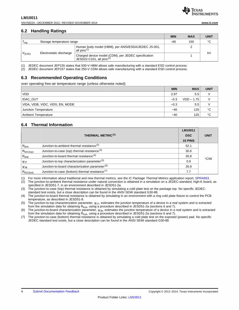
6.2 Handling RatingsMIN MAX UNIT
Tstg Storage temperature range –65 150 °CHuman body model (HBM), per ANSI/ESDA/JEDEC JS-001, 2all pins (1)
V(ESD) Electrostatic discharge kVCharged device model (CDM), per JEDEC specification 1JESD22-C101, all pins (2)
(1) JEDEC document JEP155 states that 500-V HBM allows safe manufacturing with a standard ESD control process.(2) JEDEC document JEP157 states that 250-V CDM allows safe manufacturing with a standard ESD control process.
6.3 Recommended Operating Conditionsover operating free-air temperature range (unless otherwise noted)
MIN MAX UNITVDD 2.97 5.5 VIDAC_OUT –0.3 VDD – 1.75 VVIDA, VIDB, VIDC, VIDS, EN, MODE –0.3 5.5 VJunction Temperature −40 125 °CAmbient Temperature −40 125 °C
6.4 Thermal InformationLM10011
THERMAL METRIC (1) DSC UNIT10 PINS
RθJA Junction-to-ambient thermal resistance (2) 52.1RθJC(top) Junction-to-case (top) thermal resistance (3) 30.6RθJB Junction-to-board thermal resistance (4) 26.8
°C/WψJT Junction-to-top characterization parameter (5) 0.9ψJB Junction-to-board characterization parameter (6) 26.9RθJC(bot) Junction-to-case (bottom) thermal resistance (7) 7.7
(1) For more information about traditional and new thermal metrics, see the IC Package Thermal Metrics application report, SPRA953.(2) The junction-to-ambient thermal resistance under natural convection is obtained in a simulation on a JEDEC-standard, high-K board, as
specified in JESD51-7, in an environment described in JESD51-2a.(3) The junction-to-case (top) thermal resistance is obtained by simulating a cold plate test on the package top. No specific JEDEC-
standard test exists, but a close description can be found in the ANSI SEMI standard G30-88.(4) The junction-to-board thermal resistance is obtained by simulating in an environment with a ring cold plate fixture to control the PCB
temperature, as described in JESD51-8.(5) The junction-to-top characterization parameter, ψJT, estimates the junction temperature of a device in a real system and is extracted
from the simulation data for obtaining RθJA, using a procedure described in JESD51-2a (sections 6 and 7).(6) The junction-to-board characterization parameter, ψJB, estimates the junction temperature of a device in a real system and is extracted
from the simulation data for obtaining RθJA, using a procedure described in JESD51-2a (sections 6 and 7).(7) The junction-to-case (bottom) thermal resistance is obtained by simulating a cold plate test on the exposed (power) pad. No specific
JEDEC standard test exists, but a close description can be found in the ANSI SEMI standard G30-88.Spacer
4 Submit Documentation Feedback Copyright © 2012–2014, Texas Instruments Incorporated
Product Folder Links: LM10011
LM10011www.ti.com SNVS822A –DECEMBER 2012–REVISED NOVEMBER 2014
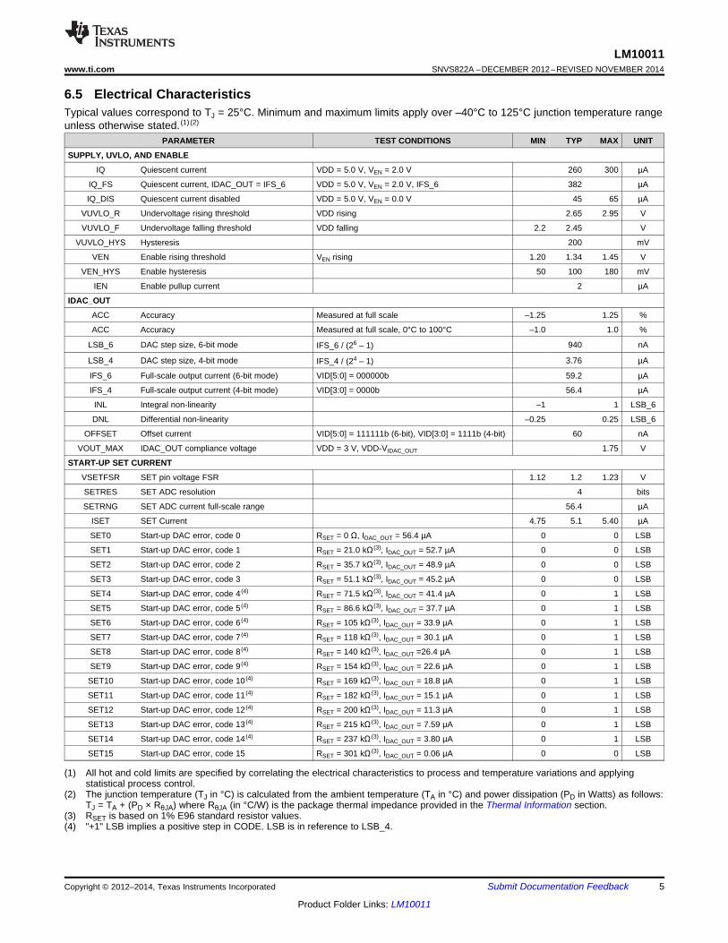
6.5 Electrical CharacteristicsTypical values correspond to TJ = 25°C. Minimum and maximum limits apply over –40°C to 125°C junction temperature rangeunless otherwise stated. (1) (2)
PARAMETER TEST CONDITIONS MIN TYP MAX UNIT
SUPPLY, UVLO, AND ENABLE
IQ Quiescent current VDD = 5.0 V, VEN = 2.0 V 260 300 µA
IQ_FS Quiescent current, IDAC_OUT = IFS_6 VDD = 5.0 V, VEN = 2.0 V, IFS_6 382 µA
IQ_DIS Quiescent current disabled VDD = 5.0 V, VEN = 0.0 V 45 65 µA
VUVLO_R Undervoltage rising threshold VDD rising 2.65 2.95 V
VUVLO_F Undervoltage falling threshold VDD falling 2.2 2.45 V
VUVLO_HYS Hysteresis 200 mV
VEN Enable rising threshold VEN rising 1.20 1.34 1.45 V
VEN_HYS Enable hysteresis 50 100 180 mV
IEN Enable pullup current 2 µA
IDAC_OUT
ACC Accuracy Measured at full scale –1.25 1.25 %
ACC Accuracy Measured at full scale, 0°C to 100°C –1.0 1.0 %
LSB_6 DAC step size, 6-bit mode 940 nAIFS_6 / (26 – 1)
LSB_4 DAC step size, 4-bit mode 3.76 µAIFS_4 / (24 – 1)
IFS_6 Full-scale output current (6-bit mode) VID[5:0] = 000000b 59.2 µA
IFS_4 Full-scale output current (4-bit mode) VID[3:0] = 0000b 56.4 µA
INL Integral non-linearity –1 1 LSB_6
DNL Differential non-linearity –0.25 0.25 LSB_6
OFFSET Offset current VID[5:0] = 111111b (6-bit), VID[3:0] = 1111b (4-bit) 60 nA
VOUT_MAX IDAC_OUT compliance voltage VDD = 3 V, VDD-VIDAC_OUT 1.75 V
START-UP SET CURRENT
VSETFSR SET pin voltage FSR 1.12 1.2 1.23 V
SETRES SET ADC resolution 4 bits
SETRNG SET ADC current full-scale range 56.4 µA
ISET SET Current 4.75 5.1 5.40 µA
SET0 Start-up DAC error, code 0 RSET = 0 Ω, IDAC_OUT = 56.4 µA 0 0 LSB
SET1 Start-up DAC error, code 1 RSET = 21.0 kΩ (3), IDAC_OUT = 52.7 µA 0 0 LSB
SET2 Start-up DAC error, code 2 RSET = 35.7 kΩ (3), IDAC_OUT = 48.9 µA 0 0 LSB
SET3 Start-up DAC error, code 3 RSET = 51.1 kΩ (3), IDAC_OUT = 45.2 µA 0 0 LSB
SET4 Start-up DAC error, code 4 (4) RSET = 71.5 kΩ (3), IDAC_OUT = 41.4 µA 0 1 LSB
SET5 Start-up DAC error, code 5 (4) RSET = 86.6 kΩ (3), IDAC_OUT = 37.7 µA 0 1 LSB
SET6 Start-up DAC error, code 6 (4) RSET = 105 kΩ (3), IDAC_OUT = 33.9 µA 0 1 LSB
SET7 Start-up DAC error, code 7 (4) RSET = 118 kΩ (3), IDAC_OUT = 30.1 µA 0 1 LSB
SET8 Start-up DAC error, code 8 (4) RSET = 140 kΩ (3), IDAC_OUT =26.4 µA 0 1 LSB
SET9 Start-up DAC error, code 9 (4) RSET = 154 kΩ (3), IDAC_OUT = 22.6 µA 0 1 LSB
SET10 Start-up DAC error, code 10 (4) RSET = 169 kΩ (3), IDAC_OUT = 18.8 µA 0 1 LSB
SET11 Start-up DAC error, code 11 (4) RSET = 182 kΩ (3), IDAC_OUT = 15.1 µA 0 1 LSB
SET12 Start-up DAC error, code 12 (4) RSET = 200 kΩ (3), IDAC_OUT = 11.3 µA 0 1 LSB
SET13 Start-up DAC error, code 13 (4) RSET = 215 kΩ (3), IDAC_OUT = 7.59 µA 0 1 LSB
SET14 Start-up DAC error, code 14 (4) RSET = 237 kΩ (3), IDAC_OUT = 3.80 µA 0 1 LSB
SET15 Start-up DAC error, code 15 RSET = 301 kΩ (3), IDAC_OUT = 0.06 µA 0 0 LSB
(1) All hot and cold limits are specified by correlating the electrical characteristics to process and temperature variations and applyingstatistical process control.
(2) The junction temperature (TJ in °C) is calculated from the ambient temperature (TA in °C) and power dissipation (PD in Watts) as follows:TJ = TA + (PD × RθJA) where RθJA (in °C/W) is the package thermal impedance provided in the Thermal Information section.
(3) RSET is based on 1% E96 standard resistor values.(4) "+1" LSB implies a positive step in CODE. LSB is in reference to LSB_4.
Copyright © 2012–2014, Texas Instruments Incorporated Submit Documentation Feedback 5
Product Folder Links: LM10011
VIDS
IDAC_OUT Current
t1
VIDA,B,C
t2
t3
t4
t1
VID[5:3] Capture VID[2:0] Capture
t5 t5
t6 t6
IDAC_OUT Update
VID[5:3] Capture
IDAC_OUT Update
tDEGLITCHVIDA,B,C,St7
VID[0:3] Hold-Time
6 BIT MODE TIMING
4 BIT MODE TIMING
t5
t6
IDAC_OUT Current
LM10011SNVS822A –DECEMBER 2012–REVISED NOVEMBER 2014 www.ti.com
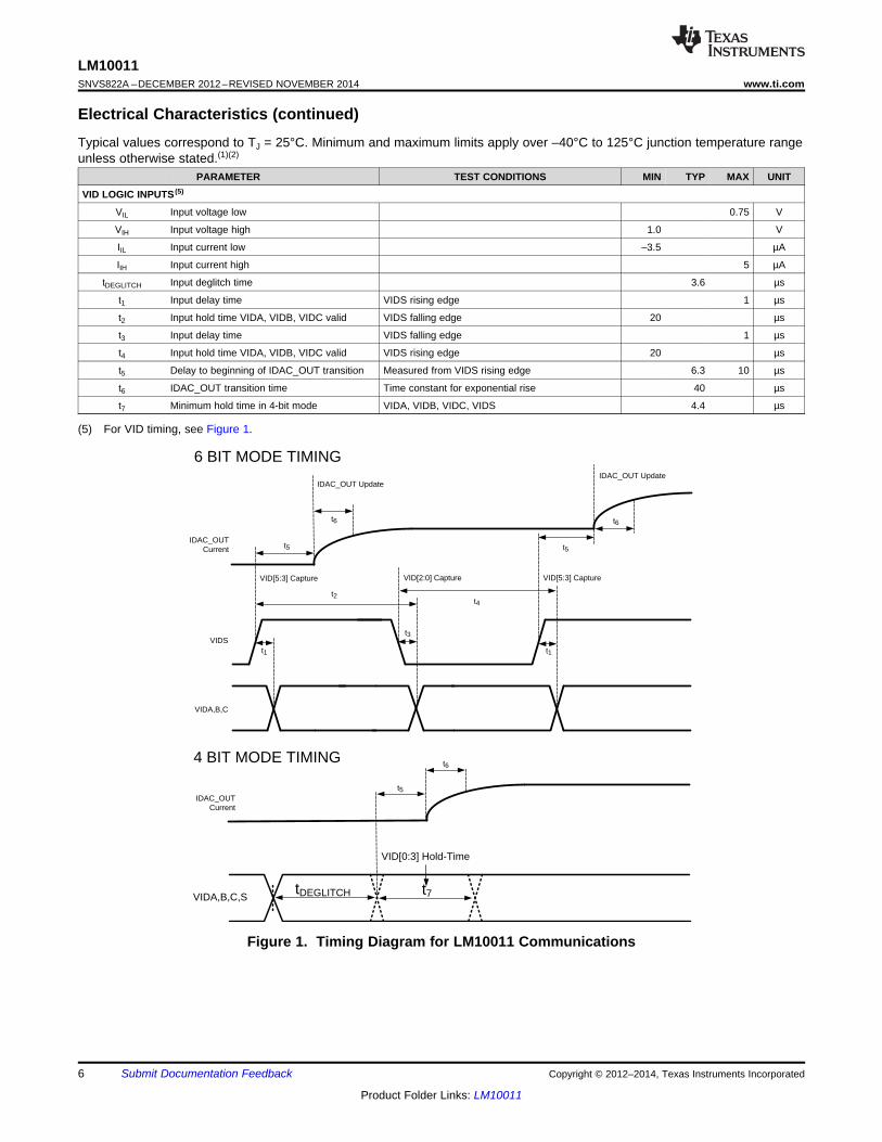
Electrical Characteristics (continued)Typical values correspond to TJ = 25°C. Minimum and maximum limits apply over –40°C to 125°C junction temperature rangeunless otherwise stated.(1)(2)
PARAMETER TEST CONDITIONS MIN TYP MAX UNIT
VID LOGIC INPUTS (5)
VIL Input voltage low 0.75 V
VIH Input voltage high 1.0 V
IIL Input current low –3.5 µA
IIH Input current high 5 µA
tDEGLITCH Input deglitch time 3.6 µs
t1 Input delay time VIDS rising edge 1 µs
t2 Input hold time VIDA, VIDB, VIDC valid VIDS falling edge 20 µs
t3 Input delay time VIDS falling edge 1 µs
t4 Input hold time VIDA, VIDB, VIDC valid VIDS rising edge 20 µs
t5 Delay to beginning of IDAC_OUT transition Measured from VIDS rising edge 6.3 10 µs
t6 IDAC_OUT transition time Time constant for exponential rise 40 µs
t7 Minimum hold time in 4-bit mode VIDA, VIDB, VIDC, VIDS 4.4 µs
(5) For VID timing, see Figure 1.
Figure 1. Timing Diagram for LM10011 Communications
6 Submit Documentation Feedback Copyright © 2012–2014, Texas Instruments Incorporated
Product Folder Links: LM10011
20
30
40
50
60
70
80
90
100
-50 -25 0 25 50 75 100 125 150
OF
FS
ET
CU
RR
EN
T (
nA
)
-81&7,21�7(03(5$785(��Û&� C006
2.4
2.45
2.5
2.55
2.6
2.65
2.7
2.75
-50 -25 0 25 50 75 100 125 150
VD
D U
VL
O V
OL
TA
GE
(V
)
-81&7,21�7(03(5$785(��Û&� C009
VDD RISING
VDD FALLING
1
1.1
1.2
1.3
1.4
1.5
1.6
-50 -25 0 25 50 75 100 125 150
CO
MP
LIA
NC
E V
OL
TA
GE
(V
)
-81&7,21�7(03(5$785(��Û&� C007
VDD = 5.5V
VDD = 3.3V
-0.5
-0.3
-0.1
0.1
0.3
0.5
-50 -25 0 25 50 75 100 125 150
GA
IN E
RR
OR
(%
)
-81&7,21�7(03(5$785(��Û&� C005
360
365
370
375
380
385
390
-50 -25 0 25 50 75 100 125 150
VD
D C
UR
RE
NT
(µA
)
-81&7,21�7(03(5$785(��Û&� C010
VDD = 2.97V
VDD = 5.0V
0
10
20
30
40
50
60
-50 -25 0 25 50 75 100 125 150
VD
D C
UR
RE
NT
(n
A)
-81&7,21�7(03(5$785(��Û&� C003
VDD = 2.97V
VDD = 5.0V
LM10011www.ti.com SNVS822A –DECEMBER 2012–REVISED NOVEMBER 2014
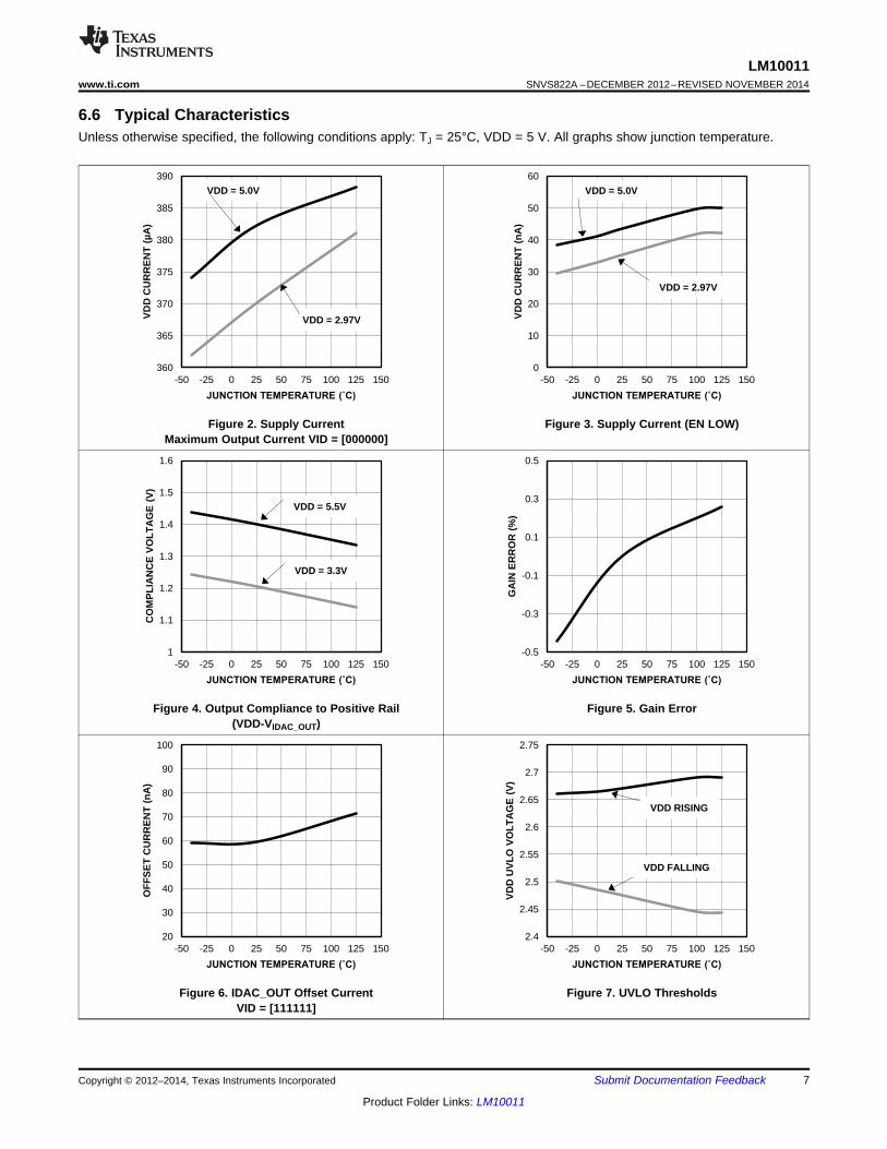
6.6 Typical CharacteristicsUnless otherwise specified, the following conditions apply: TJ = 25°C, VDD = 5 V. All graphs show junction temperature.
Figure 2. Supply Current Figure 3. Supply Current (EN LOW)Maximum Output Current VID = [000000]
Figure 4. Output Compliance to Positive Rail Figure 5. Gain Error(VDD-VIDAC_OUT)
Figure 6. IDAC_OUT Offset Current Figure 7. UVLO ThresholdsVID = [111111]
Copyright © 2012–2014, Texas Instruments Incorporated Submit Documentation Feedback 7
Product Folder Links: LM10011
-0.04
-0.02
0
0.02
0.04
0.06
0.08
0 10 20 30 40 50 60 70
DIF
FE
RE
NT
IAL
NO
N-L
INE
AR
ITY
(L
SB
)
CODE C001
���Û& -��Û& ��Û&
1.15
1.2
1.25
1.3
1.35
1.4
1.45
-50 -25 0 25 50 75 100 125 150
EN
VO
LT
AG
E (
V)
-81&7,21�7(03(5$785(��Û&� C008
RISING
FALLING
-0.25
-0.2
-0.15
-0.1
-0.05
0
0.05
0.1
0.15
0 10 20 30 40 50 60 70
INT
EG
RA
L N
ON
-LIN
EA
RIT
Y (
LS
B)
CODE C002
���Û&
��Û&
-��Û&
LM10011SNVS822A –DECEMBER 2012–REVISED NOVEMBER 2014 www.ti.com
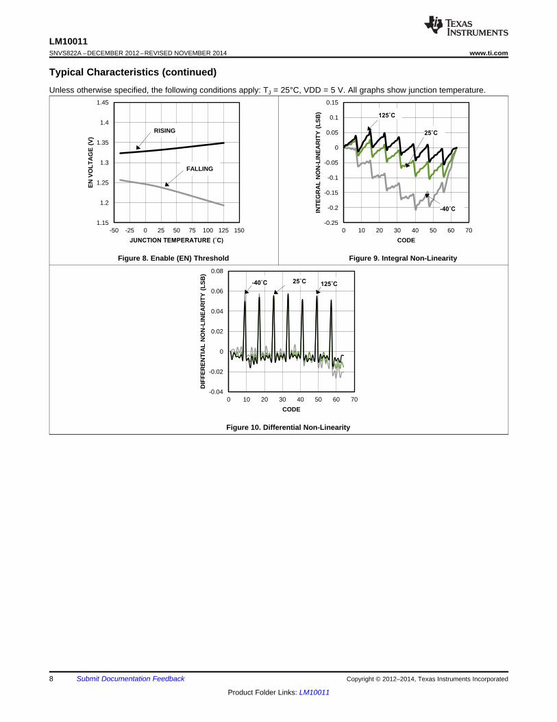
Typical Characteristics (continued)Unless otherwise specified, the following conditions apply: TJ = 25°C, VDD = 5 V. All graphs show junction temperature.
Figure 8. Enable (EN) Threshold Figure 9. Integral Non-Linearity
Figure 10. Differential Non-Linearity
8 Submit Documentation Feedback Copyright © 2012–2014, Texas Instruments Incorporated
Product Folder Links: LM10011
rise
Edge-Detector
fall
VIDAUVLO
D Q
QR
UVLO
rise
fall
VID[3]
BandgapCore
+
-
IREF
6 bitIDAC
IDAC_OUT0 ± 56.4 / 59.2 µA
(4-bit / 6-bit)
UVLO(VDD > 2.65V)
PRECISIONENABLE(1.34V)
VDD
EN
DISABLE
GND
SlewLimit
LogicReceiver
Update DAC
VIDB
VIDC
VIDS
3 µsdeglitch
LogicReceiver
3 µsdeglitch
LogicReceiver
3 µsdeglitch
LogicReceiver
6 µsdeglitch
VID[0]
D Q
QR
UVLO
D Q
QR
UVLO
rise
fall
VID[4]
VID[1]
D Q
QR
UVLO
D Q
QR
UVLO
rise
fall
VID[5]
VID[2]
D Q
QR
3 µsdeglitch
VID Start-Up Current
Set
6-BIT MODE=0
Edge-Detector
VID[0]
VID[1]
VID[2]
VID[3]
4-BIT MODE=1
MODE
RSET
3 µsdeglitch
LM10011www.ti.com SNVS822A –DECEMBER 2012–REVISED NOVEMBER 2014
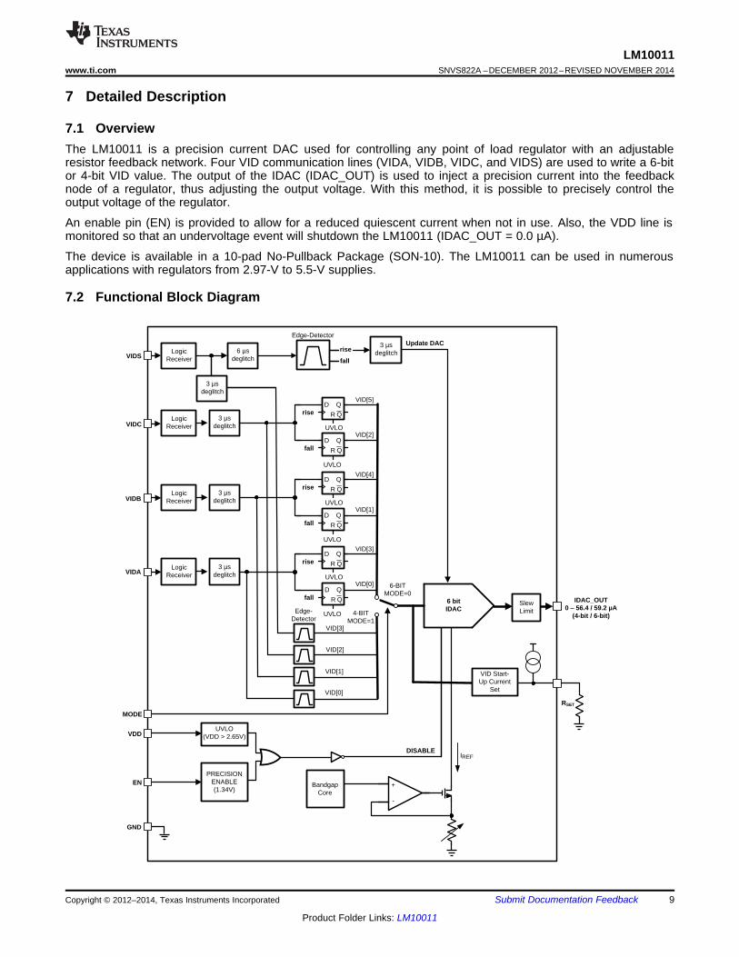
7 Detailed Description
7.1 OverviewThe LM10011 is a precision current DAC used for controlling any point of load regulator with an adjustableresistor feedback network. Four VID communication lines (VIDA, VIDB, VIDC, and VIDS) are used to write a 6-bitor 4-bit VID value. The output of the IDAC (IDAC_OUT) is used to inject a precision current into the feedbacknode of a regulator, thus adjusting the output voltage. With this method, it is possible to precisely control theoutput voltage of the regulator.
An enable pin (EN) is provided to allow for a reduced quiescent current when not in use. Also, the VDD line ismonitored so that an undervoltage event will shutdown the LM10011 (IDAC_OUT = 0.0 µA).
The device is available in a 10-pad No-Pullback Package (SON-10). The LM10011 can be used in numerousapplications with regulators from 2.97-V to 5.5-V supplies.
7.2 Functional Block Diagram
Copyright © 2012–2014, Texas Instruments Incorporated Submit Documentation Feedback 9
Product Folder Links: LM10011
Slave Regulator
FB
VOUT
LM10011
RFB1
RFB2
+- VOUT
VFB
+
-
+
-IRFB2
IDAC_OUT
IRFB1 VRFB1
+
-
IDAC_OUT
VID
LM10011
LM10011SNVS822A –DECEMBER 2012–REVISED NOVEMBER 2014 www.ti.com
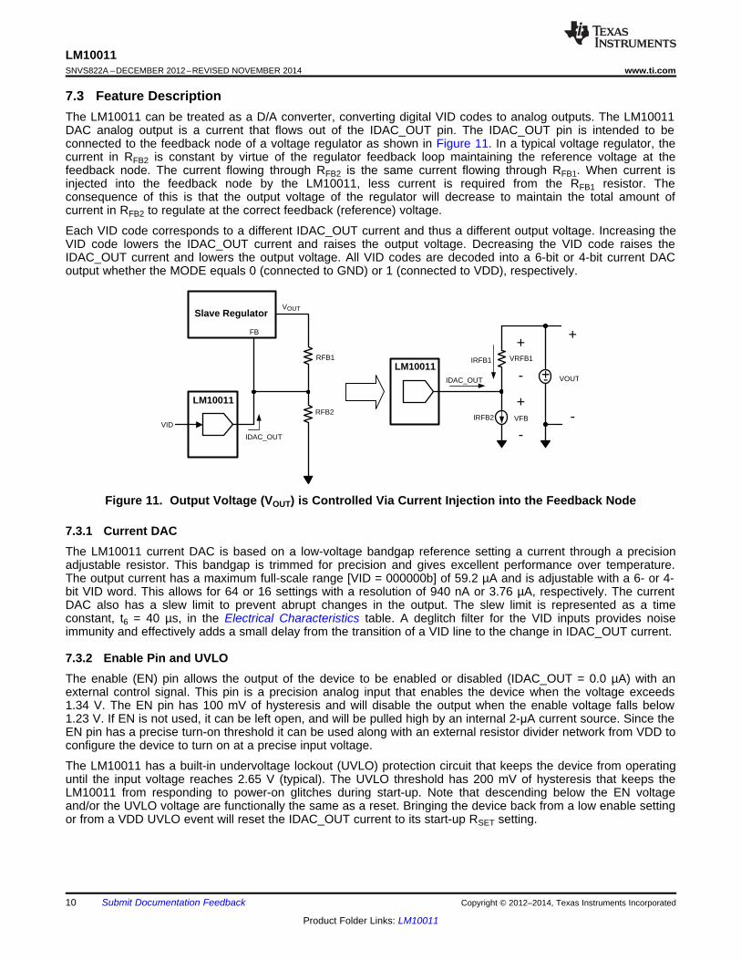
7.3 Feature DescriptionThe LM10011 can be treated as a D/A converter, converting digital VID codes to analog outputs. The LM10011DAC analog output is a current that flows out of the IDAC_OUT pin. The IDAC_OUT pin is intended to beconnected to the feedback node of a voltage regulator as shown in Figure 11. In a typical voltage regulator, thecurrent in RFB2 is constant by virtue of the regulator feedback loop maintaining the reference voltage at thefeedback node. The current flowing through RFB2 is the same current flowing through RFB1. When current isinjected into the feedback node by the LM10011, less current is required from the RFB1 resistor. Theconsequence of this is that the output voltage of the regulator will decrease to maintain the total amount ofcurrent in RFB2 to regulate at the correct feedback (reference) voltage.
Each VID code corresponds to a different IDAC_OUT current and thus a different output voltage. Increasing theVID code lowers the IDAC_OUT current and raises the output voltage. Decreasing the VID code raises theIDAC_OUT current and lowers the output voltage. All VID codes are decoded into a 6-bit or 4-bit current DACoutput whether the MODE equals 0 (connected to GND) or 1 (connected to VDD), respectively.
Figure 11. Output Voltage (VOUT) is Controlled Via Current Injection into the Feedback Node
7.3.1 Current DACThe LM10011 current DAC is based on a low-voltage bandgap reference setting a current through a precisionadjustable resistor. This bandgap is trimmed for precision and gives excellent performance over temperature.The output current has a maximum full-scale range [VID = 000000b] of 59.2 µA and is adjustable with a 6- or 4-bit VID word. This allows for 64 or 16 settings with a resolution of 940 nA or 3.76 µA, respectively. The currentDAC also has a slew limit to prevent abrupt changes in the output. The slew limit is represented as a timeconstant, t6 = 40 µs, in the Electrical Characteristics table. A deglitch filter for the VID inputs provides noiseimmunity and effectively adds a small delay from the transition of a VID line to the change in IDAC_OUT current.
7.3.2 Enable Pin and UVLOThe enable (EN) pin allows the output of the device to be enabled or disabled (IDAC_OUT = 0.0 µA) with anexternal control signal. This pin is a precision analog input that enables the device when the voltage exceeds1.34 V. The EN pin has 100 mV of hysteresis and will disable the output when the enable voltage falls below1.23 V. If EN is not used, it can be left open, and will be pulled high by an internal 2-μA current source. Since theEN pin has a precise turn-on threshold it can be used along with an external resistor divider network from VDD toconfigure the device to turn on at a precise input voltage.
The LM10011 has a built-in undervoltage lockout (UVLO) protection circuit that keeps the device from operatinguntil the input voltage reaches 2.65 V (typical). The UVLO threshold has 200 mV of hysteresis that keeps theLM10011 from responding to power-on glitches during start-up. Note that descending below the EN voltageand/or the UVLO voltage are functionally the same as a reset. Bringing the device back from a low enable settingor from a VDD UVLO event will reset the IDAC_OUT current to its start-up RSET setting.
10 Submit Documentation Feedback Copyright © 2012–2014, Texas Instruments Incorporated
Product Folder Links: LM10011
LM10011www.ti.com SNVS822A –DECEMBER 2012–REVISED NOVEMBER 2014
7.4 Device Functional ModesTable 1 lists the functional modes of the LM10011 device.
Table 1. Mode Pin SummaryMODE PIN CONNECTION LOGIC STATE DESCRIPTION
GND 0 6-bit modeVDD 1 4-bit mode
7.5 Programming
7.5.1 VID Programming, 6-Bit ModeFour pins are used to communicate with the LM10011. In 6-bit mode (MODE = 0), VIDA, VIDB, and VIDC aredata lines, while VIDS is a latching strobe that programs in the LM10011 data. As shown in the 6-bit mode timingdiagram of Figure 1, the falling edge of VIDS latches in the data from VIDA, VIDB, and VIDC as the lower threeLSB of the IDAC_OUT value, [2:0]. After a minimum hold time (t2), the rising edge of VIDS latches in the datafrom VIDA, VIDB, and VIDC as the upper three LSB of the IDAC_OUT value, [5:3]. Internally, a delay (t3,t1) onVIDS allows for the setting of all VIDA, VIDB, and VIDC lines to change simultaneously as VIDS rises or falls.
7.5.2 VID Programming, 4-Bit ModeThe LM10011 includes a 4-bit mode to facilitate parallel VID communication. In 4-bit mode (MODE = 1), VIDC,VIDB, VIDA, and VIDS are all parallel data lines. As shown in the 4-bit mode timing diagram in Figure 1, achanging edge of any of the VID communication lines will change the IDAC_OUT current to the correspondingnew 4-bit value found on the data lines. There is a 3-μs deglitch filter to eliminate spurious noise events. Thedata must overcome the deglitch time and the minimum hold time (t7) or else the IDAC_OUT pin current may notreflect the value indicated at the VID data inputs. During the hold time, no other data line can be transitioned.
As mentioned in a previous section, for both the 4-bit and 6-bit mode, the VID data word is set so that the lowestoutput current is seen at the highest VID data word (59.2 µA at a code of 0d in 6-bit mode and 56.4 µA in 4-bitmode). Conversely, the lowest current is seen at the highest VID data word (0.06 µA at 63d or 15d). During VIDoperation with the regulator, this will translate to the lowest output voltage with the lowest VID word, 0d, and thehighest output voltage with the highest VID word, 63d or 15d. The communications pins can be used with a low-voltage microcontroller with a maximum VIL of 0.75 V and a minimum VIH of 1.0 V.
7.5.3 Programming the Start-Up CurrentDepending on the value of RSET during start-up (when VDD > VUVLO_R and EN > VEN), the output current onthe IDAC_OUT pin will take on 1 of 16 discrete values corresponding to the currents available in the 4-bit mode.These discrete start-up currents can be programmed by connecting a resistor (RSET) from the SET pin to GND. Ifthe EN voltage is toggled or a UVLO is triggered during operation, the current will default back to the value set bythe RSET resistor. It takes only one VID command transition in either 4-bit or 6-bit mode to change the current tosomething other than the pre-programmed start-up current. The required RSET resistors and their correspondingstart-up currents codes can be found in Table 2.
Table 2. Start-Up–4-Bit Mode Currents with Corresponding RSET Values and Output CurrentsVID CODE NOMINAL IDAC_OUT CURRENT (µA) RSET (kΩ)0000b (0d) 56.4 00001b (1d) 52.7 21.00010b (2d) 48.9 35.70011b (3d) 45.2 51.10100b (4d) 41.4 71.50101b (5d) 37.7 86.60110b (6d) 33.9 1050111b (7d) 30.1 1181000b (8d) 26.4 1401001b (9d) 22.6 154
Copyright © 2012–2014, Texas Instruments Incorporated Submit Documentation Feedback 11
Product Folder Links: LM10011
LM10011SNVS822A –DECEMBER 2012–REVISED NOVEMBER 2014 www.ti.com
Programming (continued)Table 2. Start-Up–4-Bit Mode Currents with Corresponding RSET Values and Output Currents (continued)
VID CODE NOMINAL IDAC_OUT CURRENT (µA) RSET (kΩ)1010b (10d) 18.8 1691011b (11d) 15.1 1821100b (12d) 11.3 2001101b (13d) 7.59 2151110b (14d) 3.80 2371111b (15d) 0.06 301
Codes 0100b (4d) through 1110b (14d) will start-up into either the selected code or 1 code higher. This meansthat the output voltage of the POL may start-up into the selected output voltage or 1 LSB higher.
7.5.4 IDAC_OUT Current ValuesTable 3. IDAC_OUT Currents and Corresponding
Table 3. IDAC_OUT Currents and Corresponding VID Codes (continued)VID Codes
VID CODE (6-BIT [4-BIT]) IDAC CURRENT (µA)VID CODE (6-BIT [4-BIT]) IDAC CURRENT (µA) 32d 29.2
0d 59.2 33d 28.21d 58.3 34d 27.32d 57.4 35d [8d] 26.4
3d [0d] 56.4 36d 25.44d 55.5 37d 24.55d 54.6 38d 23.66d 53.6 39d [9d] 22.6
7d [1d] 52.7 40d 21.68d 51.7 41d 20.79d 50.8 42d 19.810d 49.8 43d [10d] 18.8
11d [2d] 48.9 44d 17.912d 48.0 45d 17.013d 47.0 46d 16.014d 46.1 47d [11d] 15.1
15d [3d] 45.2 48d 14.116d 44.2 49d 13.217d 43.3 50d 12.318d 42.3 51d [12d] 11.3
19d [4d] 41.4 52d 10.420d 40.5 53d 9.5021d 39.5 54d 8.5222d 38.6 55d [13d] 7.59
23d [5d] 37.7 56d 6.6024d 36.7 57d 5.7025d 35.7 58d 4.7426d 34.8 59d [14d] 3.80
27d [6d] 33.9 60d 2.8728d 33.0 61d 1.9329d 32.0 62d 1.0030d 31.1 63d [15d] 0.06
31d [7d] 30.1
12 Submit Documentation Feedback Copyright © 2012–2014, Texas Instruments Incorporated
Product Folder Links: LM10011
FB
PGOOD
VIN
LM21215A-1
VOUT
AGND
COMP
PVIN SW
ENCIN COUT
LF
RC1CC1
CC2
CC3
RFB1
RFB2
RC2
PGND
AVIN
CF
11-16
3
4
17
19
18
208,9,10
5,6,7
RF
SS/TRK
CSS
2optional
TSSOP-20
EN
GNDVIDA
1
10
SON-10 3 mm x 3 mm
VIDB
VIDC
VIDS9
8
7
4 VDDIDAC_OUT
3
20 - 59.2 µA
LM10011
SYNC1
CVDD
3V to 5.5V
CVDD
CBYPASS
VCNTL[3]
VCNTL[2]
VCNTL[1]
VCNTL[0]
TMS320C6670/TMS320C6678
0.7V to 1.1V
DVDD18RPU1:4
MODE5
RSET
SET6
LM10011www.ti.com SNVS822A –DECEMBER 2012–REVISED NOVEMBER 2014
8 Application and Implementation
NOTEInformation in the following applications sections is not part of the TI componentspecification, and TI does not warrant its accuracy or completeness. TI’s customers areresponsible for determining suitability of components for their purposes. Customers shouldvalidate and test their design implementation to confirm system functionality.
8.1 Application InformationLM10011 is a precision, digitally programmable device used for controlling the dc-dc converter output voltage.The LM10011 GUI design tool is available at www.ti.com/product/LM10011 and can be used to program anyvoltage regulator output to a desired range and resolution. The GUI enables changing the output voltage of theon-board POL based on direct user input. It is also able to assist the power designer in selecting the correctexternal components needed for any given application.
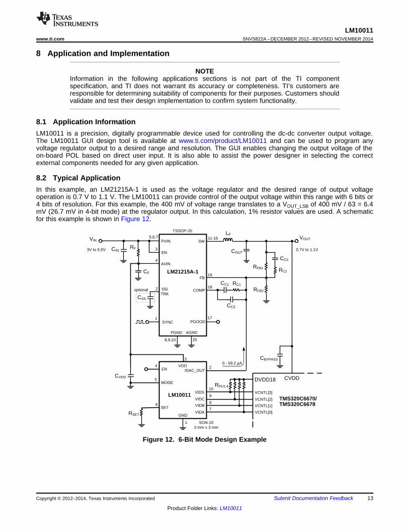
8.2 Typical ApplicationIn this example, an LM21215A-1 is used as the voltage regulator and the desired range of output voltageoperation is 0.7 V to 1.1 V. The LM10011 can provide control of the output voltage within this range with 6 bits or4 bits of resolution. For this example, the 400 mV of voltage range translates to a VOUT_LSB of 400 mV / 63 = 6.4mV (26.7 mV in 4-bit mode) at the regulator output. In this calculation, 1% resistor values are used. A schematicfor this example is shown in Figure 12.
Figure 12. 6-Bit Mode Design Example
Copyright © 2012–2014, Texas Instruments Incorporated Submit Documentation Feedback 13
Product Folder Links: LM10011
RFB1 = 6.8k
6.4mV = 0.940µA x RFB1
IDAC_OUT = VFB x 1+RFB1
RFB2- VOUT
RFB1
1
VOUT_LSB = LSB x RFB1
VOUT = VFB x 1+RFB1
RFB2- IDAC_OUT x RFB1
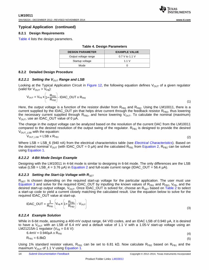
LM10011SNVS822A –DECEMBER 2012–REVISED NOVEMBER 2014 www.ti.com
Typical Application (continued)8.2.1 Design RequirementsTable 4 lists the design parameters.
Table 4. Design ParametersDESIGN PARAMETER EXAMPLE VALUEOutput voltage range 0.7 V to 1.1 V
Startup voltage 1.1 VMode 0
8.2.2 Detailed Design Procedure
8.2.2.1 Setting the VOUT Range and LSBLooking at the Typical Application Circuit in Figure 12, the following equation defines VOUT of a given regulator(valid for VOUT > VFB):
(1)
Here, the output voltage is a function of the resistor divider from RFB1 and RFB2. Using the LM10011, there is acurrent supplied by the IDAC_OUT pin that helps drive current through the feedback resistor RFB2, thus loweringthe necessary current supplied through RFB1, and hence lowering VOUT. To calculate the nominal (maximum)VOUT, use an IDAC_OUT value of 0 µA.
The change in the output voltage can be analyzed based on the resolution of the current DAC from the LM10011compared to the desired resolution of the output swing of the regulator. RFB1 is designed to provide the desiredVOUT_LSB with the equation:
(2)
Where LSB = LSB_6 (940 nA) from the electrical characteristics table (see Electrical Characteristics). Based onthe desired nominal VOUT (with IDAC_OUT = 0 µA) and the calculated RFB1 from Equation 2, RFB2 can be solvedusing Equation 1.
8.2.2.2 4-Bit Mode Design ExampleDesigning with the LM10011 in 4-bit mode is similar to designing in 6-bit mode. The only differences are the LSBvalue (LSB = LSB_4 = 3.76 µA) in Equation 2 and full-scale current range (IDAC_OUT = 56.4 µA).
8.2.2.3 Setting the Start-Up Voltage with RSET
RSET is chosen depending on the required start-up voltage for the particular application. The user must useEquation 3 and solve for the required IDAC_OUT by inputting the known values of RFB1 and RFB2, VFB, and thedesired start-up output voltage, VOUT. Once IDAC_OUT is solved for, choose an RSET based on Table 2 to selecta start-up code to yield a current closely matching the calculated result. Use the equation below to solve for therequired IDAC_OUT value at start-up.
(3)
8.2.2.4 Example SolutionWhile in 6-bit mode, assuming a 400-mV output range, 64 VID codes, and an IDAC LSB of 0.940 µA, it is desiredto have a VOUT with an LSB of 6.4 mV and a default value of 1.1 V with a 1.05-V start-up voltage using anLM21215A-1 regulator (VFB = 0.6 V):
(4)(5)
Using 1% standard resistor values, RFB1 can be set to 6.81 kΩ. Now calculate RFB2 based on RFB1 and themaximum VOUT of 1.1 V using Equation 1.14 Submit Documentation Feedback Copyright © 2012–2014, Texas Instruments Incorporated
Product Folder Links: LM10011
6-Bit VID Code (Decimal)
Out
put V
olta
ge (
V)
0 5 10 15 20 25 30 35 40 45 50 55 60 650.690.720.750.780.810.840.87
0.90.930.960.991.021.051.081.111.14
VIN = 2.9VVIN = 5.5V
IDAC_OUT = 0.6V x 1+6.81k 8.06k
- 1.05V 6.81k
1= 8.36µA
RFB2 = 8.1k
1.1V = .6V x 1+6.81k
RFB2-0V
LM10011www.ti.com SNVS822A –DECEMBER 2012–REVISED NOVEMBER 2014
(6)(7)
Using 1% standard resistor values, RFB2 can be set to 8.06 kΩ. This will yield a regulator output range of 0.704 V(CODE 0d) to 1.107 V (CODE 63d). Values calculated here will be dependent on the accuracy of the regulator,the LM10011 IDAC_OUT, and the resistor values used in the circuit.
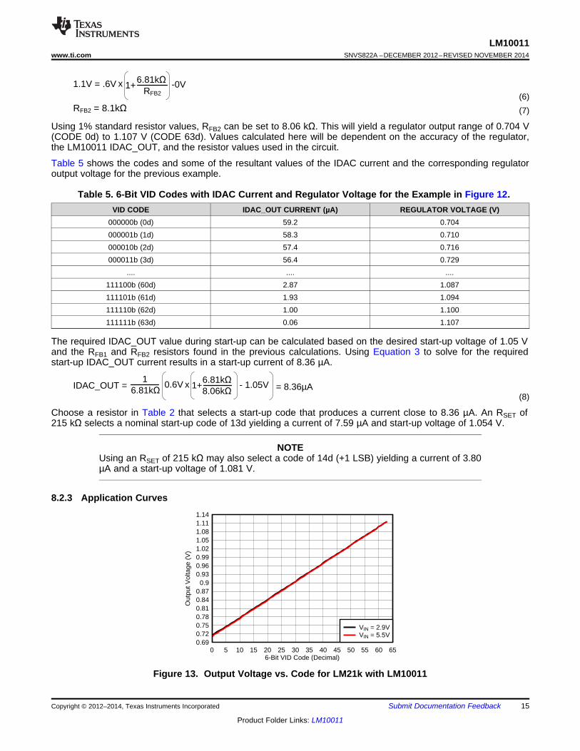
Table 5 shows the codes and some of the resultant values of the IDAC current and the corresponding regulatoroutput voltage for the previous example.
Table 5. 6-Bit VID Codes with IDAC Current and Regulator Voltage for the Example in Figure 12.VID CODE IDAC_OUT CURRENT (µA) REGULATOR VOLTAGE (V)
000000b (0d) 59.2 0.704000001b (1d) 58.3 0.710000010b (2d) 57.4 0.716000011b (3d) 56.4 0.729
.... .... ....111100b (60d) 2.87 1.087111101b (61d) 1.93 1.094111110b (62d) 1.00 1.100111111b (63d) 0.06 1.107
The required IDAC_OUT value during start-up can be calculated based on the desired start-up voltage of 1.05 Vand the RFB1 and RFB2 resistors found in the previous calculations. Using Equation 3 to solve for the requiredstart-up IDAC_OUT current results in a start-up current of 8.36 µA.
(8)
Choose a resistor in Table 2 that selects a start-up code that produces a current close to 8.36 µA. An RSET of215 kΩ selects a nominal start-up code of 13d yielding a current of 7.59 µA and start-up voltage of 1.054 V.
NOTEUsing an RSET of 215 kΩ may also select a code of 14d (+1 LSB) yielding a current of 3.80µA and a start-up voltage of 1.081 V.
8.2.3 Application Curves
Figure 13. Output Voltage vs. Code for LM21k with LM10011
Copyright © 2012–2014, Texas Instruments Incorporated Submit Documentation Feedback 15
Product Folder Links: LM10011
LM10011SNVS822A –DECEMBER 2012–REVISED NOVEMBER 2014 www.ti.com
9 Power Supply RecommendationsThe LM10011 can be driven from a PWM controller VDD pin or from the VIN supply pin as shown in Figure 12. Toensure reliable operation, the LM10011 VDD input power supply must be limited to 6 V maximum.
10 Layout
10.1 Layout GuidelinesThe following guidelines should be followed when designing the PC board for the LM10011:• Place the LM10011 close to the regulator feedback pin to minimize the FB trace length.• Place a small capacitor, CVDD, (1 nF) directly adjacent to the VDD and GND pins of the LM10011 to help
minimize transients which may occur on the input supply line.• The high-current path from the board input to the load and the return path should be parallel and close to
each other to minimize loop inductance.• The ground connections for the various components around the LM10011 should be connected directly to
each other, and to the LM10011 GND pins, and then connected to the system ground at one point. Do notconnect the various component grounds to each other through the high-current ground line.
• For additional information about the operation of the regulator, please consult the respective data sheet andapplication notes on the respective evaluation boards.
16 Submit Documentation Feedback Copyright © 2012–2014, Texas Instruments Incorporated
Product Folder Links: LM10011
LM10011www.ti.com SNVS822A –DECEMBER 2012–REVISED NOVEMBER 2014
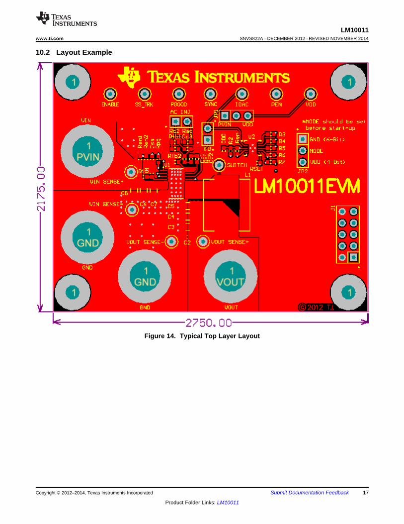
10.2 Layout Example
Figure 14. Typical Top Layer Layout
Copyright © 2012–2014, Texas Instruments Incorporated Submit Documentation Feedback 17
Product Folder Links: LM10011
LM10011SNVS822A –DECEMBER 2012–REVISED NOVEMBER 2014 www.ti.com
11 Device and Documentation Support
11.1 TrademarksAll trademarks are the property of their respective owners.
11.2 Electrostatic Discharge CautionThese devices have limited built-in ESD protection. The leads should be shorted together or the device placed in conductive foamduring storage or handling to prevent electrostatic damage to the MOS gates.
11.3 GlossarySLYZ022 — TI Glossary.
This glossary lists and explains terms, acronyms, and definitions.
12 Mechanical, Packaging, and Orderable InformationThe following pages include mechanical, packaging, and orderable information. This information is the mostcurrent data available for the designated devices. This data is subject to change without notice and revision ofthis document. For browser-based versions of this data sheet, refer to the left-hand navigation.
18 Submit Documentation Feedback Copyright © 2012–2014, Texas Instruments Incorporated
Product Folder Links: LM10011
PACKAGE OPTION ADDENDUM
www.ti.com 20-Oct-2014
Addendum-Page 1
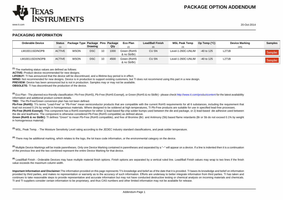
PACKAGING INFORMATION
Orderable Device Status(1)
Package Type PackageDrawing
Pins PackageQty
Eco Plan(2)
Lead/Ball Finish(6)
MSL Peak Temp(3)
Op Temp (°C) Device Marking(4/5)
Samples
LM10011SD/NOPB ACTIVE WSON DSC 10 1000 Green (RoHS& no Sb/Br)
CU SN Level-1-260C-UNLIM -40 to 125 L271B
LM10011SDX/NOPB ACTIVE WSON DSC 10 4500 Green (RoHS& no Sb/Br)
CU SN Level-1-260C-UNLIM -40 to 125 L271B
(1) The marketing status values are defined as follows:ACTIVE: Product device recommended for new designs.LIFEBUY: TI has announced that the device will be discontinued, and a lifetime-buy period is in effect.NRND: Not recommended for new designs. Device is in production to support existing customers, but TI does not recommend using this part in a new design.PREVIEW: Device has been announced but is not in production. Samples may or may not be available.OBSOLETE: TI has discontinued the production of the device.
(2) Eco Plan - The planned eco-friendly classification: Pb-Free (RoHS), Pb-Free (RoHS Exempt), or Green (RoHS & no Sb/Br) - please check http://www.ti.com/productcontent for the latest availabilityinformation and additional product content details.TBD: The Pb-Free/Green conversion plan has not been defined.Pb-Free (RoHS): TI's terms "Lead-Free" or "Pb-Free" mean semiconductor products that are compatible with the current RoHS requirements for all 6 substances, including the requirement thatlead not exceed 0.1% by weight in homogeneous materials. Where designed to be soldered at high temperatures, TI Pb-Free products are suitable for use in specified lead-free processes.Pb-Free (RoHS Exempt): This component has a RoHS exemption for either 1) lead-based flip-chip solder bumps used between the die and package, or 2) lead-based die adhesive used betweenthe die and leadframe. The component is otherwise considered Pb-Free (RoHS compatible) as defined above.Green (RoHS & no Sb/Br): TI defines "Green" to mean Pb-Free (RoHS compatible), and free of Bromine (Br) and Antimony (Sb) based flame retardants (Br or Sb do not exceed 0.1% by weightin homogeneous material)
(3) MSL, Peak Temp. - The Moisture Sensitivity Level rating according to the JEDEC industry standard classifications, and peak solder temperature.
(4) There may be additional marking, which relates to the logo, the lot trace code information, or the environmental category on the device.
(5) Multiple Device Markings will be inside parentheses. Only one Device Marking contained in parentheses and separated by a "~" will appear on a device. If a line is indented then it is a continuationof the previous line and the two combined represent the entire Device Marking for that device.
(6) Lead/Ball Finish - Orderable Devices may have multiple material finish options. Finish options are separated by a vertical ruled line. Lead/Ball Finish values may wrap to two lines if the finishvalue exceeds the maximum column width.
Important Information and Disclaimer:The information provided on this page represents TI's knowledge and belief as of the date that it is provided. TI bases its knowledge and belief on informationprovided by third parties, and makes no representation or warranty as to the accuracy of such information. Efforts are underway to better integrate information from third parties. TI has taken andcontinues to take reasonable steps to provide representative and accurate information but may not have conducted destructive testing or chemical analysis on incoming materials and chemicals.TI and TI suppliers consider certain information to be proprietary, and thus CAS numbers and other limited information may not be available for release.
PACKAGE OPTION ADDENDUM
www.ti.com 20-Oct-2014
Addendum-Page 2
In no event shall TI's liability arising out of such information exceed the total purchase price of the TI part(s) at issue in this document sold by TI to Customer on an annual basis.
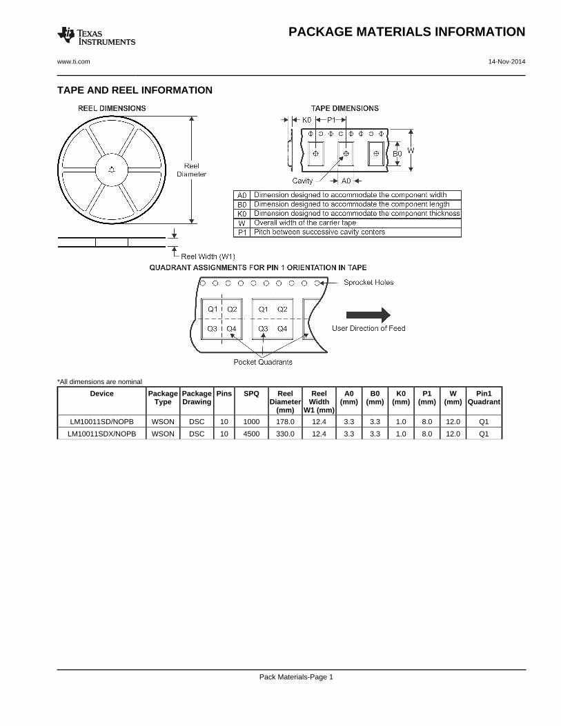
TAPE AND REEL INFORMATION
*All dimensions are nominal
Device PackageType
PackageDrawing
Pins SPQ ReelDiameter
(mm)
ReelWidth
W1 (mm)
A0(mm)
B0(mm)
K0(mm)
P1(mm)
W(mm)
Pin1Quadrant
LM10011SD/NOPB WSON DSC 10 1000 178.0 12.4 3.3 3.3 1.0 8.0 12.0 Q1
LM10011SDX/NOPB WSON DSC 10 4500 330.0 12.4 3.3 3.3 1.0 8.0 12.0 Q1
PACKAGE MATERIALS INFORMATION
www.ti.com 14-Nov-2014
Pack Materials-Page 1
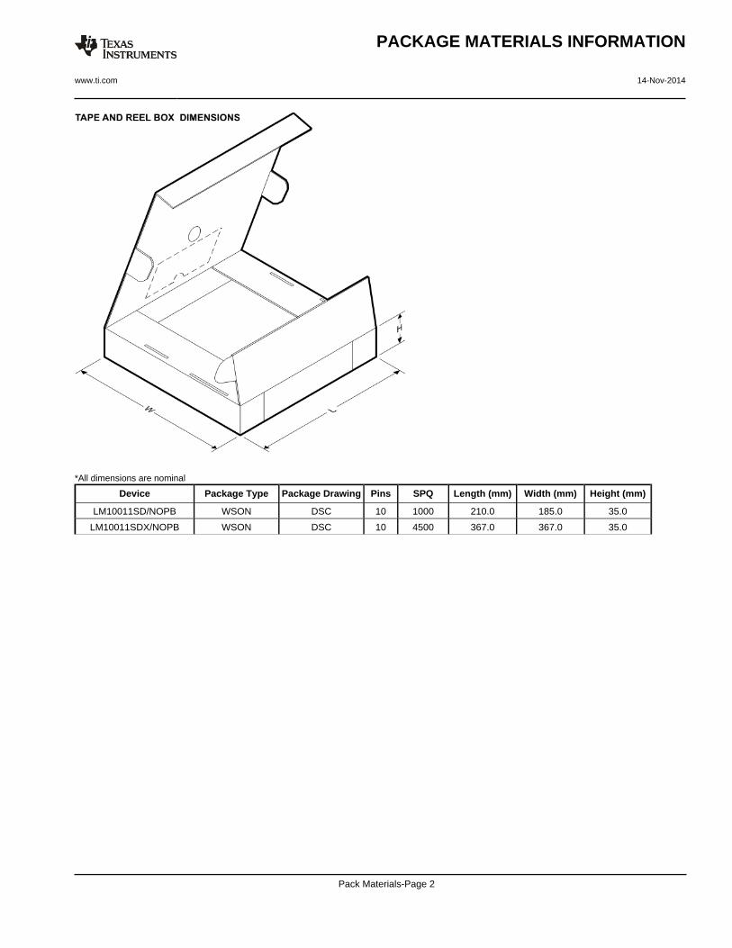
*All dimensions are nominal
Device Package Type Package Drawing Pins SPQ Length (mm) Width (mm) Height (mm)
LM10011SD/NOPB WSON DSC 10 1000 210.0 185.0 35.0
LM10011SDX/NOPB WSON DSC 10 4500 367.0 367.0 35.0
PACKAGE MATERIALS INFORMATION
www.ti.com 14-Nov-2014
Pack Materials-Page 2
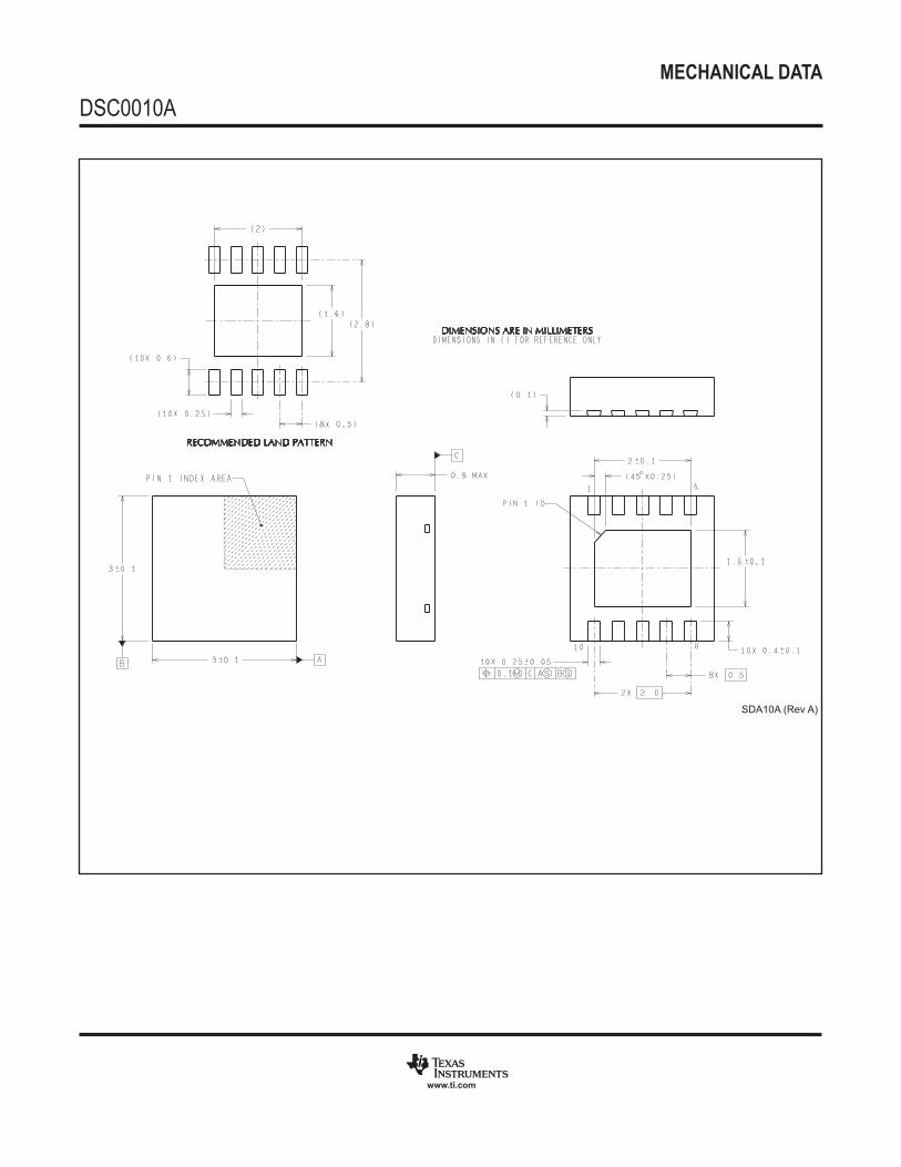
MECHANICAL DATA
DSC0010A
www.ti.com
SDA10A (Rev A)
IMPORTANT NOTICE
Texas Instruments Incorporated (TI) reserves the right to make corrections, enhancements, improvements and other changes to itssemiconductor products and services per JESD46, latest issue, and to discontinue any product or service per JESD48, latest issue. Buyersshould obtain the latest relevant information before placing orders and should verify that such information is current and complete.TI’s published terms of sale for semiconductor products (http://www.ti.com/sc/docs/stdterms.htm) apply to the sale of packaged integratedcircuit products that TI has qualified and released to market. Additional terms may apply to the use or sale of other types of TI products andservices.Reproduction of significant portions of TI information in TI data sheets is permissible only if reproduction is without alteration and isaccompanied by all associated warranties, conditions, limitations, and notices. TI is not responsible or liable for such reproduceddocumentation. Information of third parties may be subject to additional restrictions. Resale of TI products or services with statementsdifferent from or beyond the parameters stated by TI for that product or service voids all express and any implied warranties for theassociated TI product or service and is an unfair and deceptive business practice. TI is not responsible or liable for any such statements.Buyers and others who are developing systems that incorporate TI products (collectively, “Designers”) understand and agree that Designersremain responsible for using their independent analysis, evaluation and judgment in designing their applications and that Designers havefull and exclusive responsibility to assure the safety of Designers' applications and compliance of their applications (and of all TI productsused in or for Designers’ applications) with all applicable regulations, laws and other applicable requirements. Designer represents that, withrespect to their applications, Designer has all the necessary expertise to create and implement safeguards that (1) anticipate dangerousconsequences of failures, (2) monitor failures and their consequences, and (3) lessen the likelihood of failures that might cause harm andtake appropriate actions. Designer agrees that prior to using or distributing any applications that include TI products, Designer willthoroughly test such applications and the functionality of such TI products as used in such applications.TI’s provision of technical, application or other design advice, quality characterization, reliability data or other services or information,including, but not limited to, reference designs and materials relating to evaluation modules, (collectively, “TI Resources”) are intended toassist designers who are developing applications that incorporate TI products; by downloading, accessing or using TI Resources in anyway, Designer (individually or, if Designer is acting on behalf of a company, Designer’s company) agrees to use any particular TI Resourcesolely for this purpose and subject to the terms of this Notice.TI’s provision of TI Resources does not expand or otherwise alter TI’s applicable published warranties or warranty disclaimers for TIproducts, and no additional obligations or liabilities arise from TI providing such TI Resources. TI reserves the right to make corrections,enhancements, improvements and other changes to its TI Resources. TI has not conducted any testing other than that specificallydescribed in the published documentation for a particular TI Resource.Designer is authorized to use, copy and modify any individual TI Resource only in connection with the development of applications thatinclude the TI product(s) identified in such TI Resource. NO OTHER LICENSE, EXPRESS OR IMPLIED, BY ESTOPPEL OR OTHERWISETO ANY OTHER TI INTELLECTUAL PROPERTY RIGHT, AND NO LICENSE TO ANY TECHNOLOGY OR INTELLECTUAL PROPERTYRIGHT OF TI OR ANY THIRD PARTY IS GRANTED HEREIN, including but not limited to any patent right, copyright, mask work right, orother intellectual property right relating to any combination, machine, or process in which TI products or services are used. Informationregarding or referencing third-party products or services does not constitute a license to use such products or services, or a warranty orendorsement thereof. Use of TI Resources may require a license from a third party under the patents or other intellectual property of thethird party, or a license from TI under the patents or other intellectual property of TI.TI RESOURCES ARE PROVIDED “AS IS” AND WITH ALL FAULTS. TI DISCLAIMS ALL OTHER WARRANTIES ORREPRESENTATIONS, EXPRESS OR IMPLIED, REGARDING RESOURCES OR USE THEREOF, INCLUDING BUT NOT LIMITED TOACCURACY OR COMPLETENESS, TITLE, ANY EPIDEMIC FAILURE WARRANTY AND ANY IMPLIED WARRANTIES OFMERCHANTABILITY, FITNESS FOR A PARTICULAR PURPOSE, AND NON-INFRINGEMENT OF ANY THIRD PARTY INTELLECTUALPROPERTY RIGHTS. TI SHALL NOT BE LIABLE FOR AND SHALL NOT DEFEND OR INDEMNIFY DESIGNER AGAINST ANY CLAIM,INCLUDING BUT NOT LIMITED TO ANY INFRINGEMENT CLAIM THAT RELATES TO OR IS BASED ON ANY COMBINATION OFPRODUCTS EVEN IF DESCRIBED IN TI RESOURCES OR OTHERWISE. IN NO EVENT SHALL TI BE LIABLE FOR ANY ACTUAL,DIRECT, SPECIAL, COLLATERAL, INDIRECT, PUNITIVE, INCIDENTAL, CONSEQUENTIAL OR EXEMPLARY DAMAGES INCONNECTION WITH OR ARISING OUT OF TI RESOURCES OR USE THEREOF, AND REGARDLESS OF WHETHER TI HAS BEENADVISED OF THE POSSIBILITY OF SUCH DAMAGES.Unless TI has explicitly designated an individual product as meeting the requirements of a particular industry standard (e.g., ISO/TS 16949and ISO 26262), TI is not responsible for any failure to meet such industry standard requirements.Where TI specifically promotes products as facilitating functional safety or as compliant with industry functional safety standards, suchproducts are intended to help enable customers to design and create their own applications that meet applicable functional safety standardsand requirements. Using products in an application does not by itself establish any safety features in the application. Designers mustensure compliance with safety-related requirements and standards applicable to their applications. Designer may not use any TI products inlife-critical medical equipment unless authorized officers of the parties have executed a special contract specifically governing such use.Life-critical medical equipment is medical equipment where failure of such equipment would cause serious bodily injury or death (e.g., lifesupport, pacemakers, defibrillators, heart pumps, neurostimulators, and implantables). Such equipment includes, without limitation, allmedical devices identified by the U.S. Food and Drug Administration as Class III devices and equivalent classifications outside the U.S.TI may expressly designate certain products as completing a particular qualification (e.g., Q100, Military Grade, or Enhanced Product).Designers agree that it has the necessary expertise to select the product with the appropriate qualification designation for their applicationsand that proper product selection is at Designers’ own risk. Designers are solely responsible for compliance with all legal and regulatoryrequirements in connection with such selection.Designer will fully indemnify TI and its representatives against any damages, costs, losses, and/or liabilities arising out of Designer’s non-compliance with the terms and provisions of this Notice.
Mailing Address: Texas Instruments, Post Office Box 655303, Dallas, Texas 75265Copyright © 2017, Texas Instruments Incorporated