Embed Size (px)
Citation preview

3000 Service Manual

3000 Service Manual
Copyright © Acorn Computers Limited 1989
Neither the whole nor any part of the information contained in, nor the product described in this Guide may be adapted or reproduced in any material form except with the prior written approval of Acorn Computers Limited.
The products described in this manual are subject to continuous development and improvement. All information of a technical nature and particulars of the products and their use (including the information and particulars in this Manual) are given by Acorn Computers Limited in good faith. However, Acorn Computers Limited cannot accept any liability for any loss or damage arising from the use of any information or particulars in this manual, or any incorrect use of the products. All maintenance and service on the products must be carried out by Acorn Computers' authorised dealers or Approved Service Centres. Acorn Computers Limited can accept no liability whatsoever for any loss or damage caused by service, maintenance or repair by unauthorised personnel.
All correspondence should be addressed to: Customer ServiceAcorn Computers LimitedFulbourn RoadCherry Hinton Cambridge CB1 4JN
Information can also be obtained from the Acorn Support Information Database (SID). This is an on-line viewdata system available to registered SID users. Initially, access SID on Cambridge (0223) 243642: this will allow you to inspect the system and use a response frame for registration.
ACORN and ECONET are trademarks of Acorn Computers Limited.
IBM is a trademark of International Business Machines Corporation.
Within this publication, the term 'BBC' is used as an abbreviation for 'British Broadcasting Corporation'.
Published September 1989Published by Acorn Computers Technical Publications Department Part number 0480,050 Issue 1
2
3000 Service Manual
Contents
System description 5Introduction 5General 5The I/O system 6The sound system 13The keyboard and mouse 14Floppy disc drive 19Power supply 19Links 20Plugs 21Sockets 21Changes between Issue A and Issue 1 PCBs 23
A3000 expansion 25Internal expansion 25External expansion 29
Disassembly and reassembly 31
Fault diagnosis 33Introduction 33Checking a 'dead' computer 34Functional tests 36Main computer tests 38Upgrade tests 42
Main PCB fault diagnosis & repair 45Introduction 45System failure 46Video faults 46Peripheral faults 47Test ROMs 48
Parts lists 51Appendix A: Serial port loopback plug 55
Appendix B: Earth continuity testing 57
Drawings
A3000 final assembly diagram User Port / MIDI circuit diagram Internal upgrade diagram External podule fixing diagram
Main PCB circuit diagram )Main PCB top assembly diagram ) boundMain PCB bottom assembly diagram ) separately
3

3000 Service Manual
4

3000 Service Manual
System description IntroductionThe A3000 computer is built around the ARM chip set, comprising the Acorn Risc Machine (ARM) itself, the Memory Controller (MEMC), Video Controller (VIDC)
and Input Output Controller (IOC).A block diagram of the A3000 is shown below:
GeneralThe ARM IC is a pipelined, 32-bit reduced instruction set microprocessor which accepts instructions and manipulates data via a high speed 32-bit data bus and 26-bit address bus, giving a 64 Mbyte uniform address space. The ARM supports virtual memory systems using a simple but powerful instruction set with good high-level language compiler support.
MEMC acts as the interface between the ARM, the Video and I/0 Controllers, Read-Only Memory (ROM) and Dynamic memory devices (DRAM), providing all the critical system timing signals including processor clocks.
1 or 2 Mbyte of DRAM is connected to MEMC which provides all signals and refresh operations. A Logical to Physical Translator maps the Physical Memory into a 32 Mbyte Logical address space (with three levels of protection) allowing Virtual Memory and Multi-Tasking operations to be implemented. Fast page mode DRAM
accesses are used to maximise memory bandwidth. VIDC requests data from the RAM when required and buffers it in one of three FIFOs before using it. Data is requested in blocks of four 32-bit words, allowing efficient use of paged-mode DRAM without locking the system data bus for long periods.
MEMC supports Direct Memory Access (DMA) operations with a set of programmable DMA Address Generators which provide a circular buffer for Video data, a linear buffer for Cursor data and a double buffer for Sound data.
The Input Output Controller (IOC) controls the I/O bus and expansion cards, and provides basic functions such as the keyboard interface, system timers, interrupt masks and control registers. It supports a number of different peripheral cycles, and all I/O accesses are memory mapped.
System description 5

3000 Service Manual
VIDC takes video data from memory under DMA control, serialises it and passes it through a colour look-up palette, then converts it to analogue signals for driving the CRT guns. VIDC also controls all the display timing parameters and controls the position and pattern of the cursor sprite. In addition, it
incorporates an exponential Digital to Analogue Converter (DAC) and stereo image table for the generation of high quality sound from data in the DRAM.
VIDC is a highly programmable device, offering a very wide choice of display formats. The colour look-up palette which drives the three on-chip DACs is 13 bits wide, offering a choice from 4096 colours or an external video source.
The cursor sprite is 32 pixels wide and any number of rasters high. Three simultaneous colours (again from a choice of 4096) are supported and any pixel can be defined as transparent, making possible cursors of many shapes. It can be positioned anywhere on the screen.
The sound system implemented on the device can support up to 8 channels, each with a separate stereo position.
The I/O systemThe I/O system is controlled by the I/O Controller (IOC) and the Memory Controller (MEMC). The I/O Bus supports all the internal peripherals and the expansion cards. Details of the expansion bus can be found in the chapter entitled 'A3000 expansion'.
This section is intended to give the reader a general understanding of the A3000 I/O system and should not be used to program the I/O system directly. The implementation details are liable to change at any time and only the published software interfaces should be used to manipulate the I/O system. Future systems may have a different implementation of the I/O system, and in particular the addresses (and number) of expansion card locations may move. For this reason, and to ensure that any device may be plugged into any slot, all driver code for expansion cards must be relocatable. References to the direct expansion card addresses should never be used. It is up to the machine operating system, in conjunction with the expansion card ID, to determine the address at which an expansion card should be accessed. To this extent, some of the following sections are for background information only.
6 System description
3000 Service Manual
System architectureThe I/O system (which includes expansion card devices) consists of a 16-bit data bus (BD[0:15]) a buffered address bus (LA[2:21]) and various control and timing signals. The I/O data bus is independent of the main 32-bit system data bus, being separated from it by bidirectional latches and buffers. In this way the I/0 data bus can run at much slower speeds than the main system bus to cater for slower peripheral devices. The latches between the two buses, and hence the I/O bus timing are controlled by IOC. IOC caters for 4 different cycle speeds (slow, medium, fast and synchronous).
A typical A3000 I/O system is shown in the diagram on the previous page. For clarity, the data and address buses are omitted from this diagram.
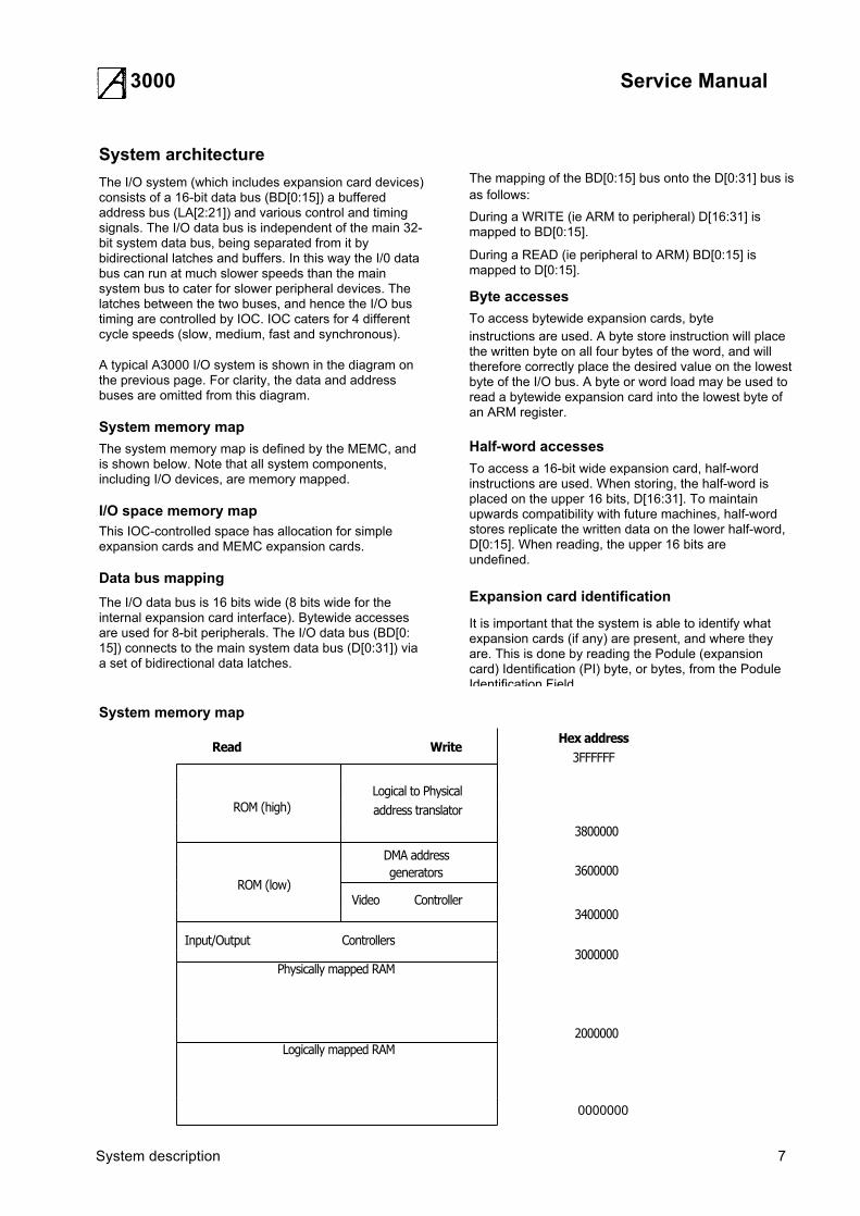
System memory mapThe system memory map is defined by the MEMC, and is shown below. Note that all system components, including I/O devices, are memory mapped.
I/O space memory mapThis IOC-controlled space has allocation for simple expansion cards and MEMC expansion cards.
Data bus mappingThe I/O data bus is 16 bits wide (8 bits wide for the internal expansion card interface). Bytewide accesses are used for 8-bit peripherals. The I/O data bus (BD[0:15]) connects to the main system data bus (D[0:31]) via a set of bidirectional data latches.
System memory map
The mapping of the BD[0:15] bus onto the D[0:31] bus is as follows:
During a WRITE (ie ARM to peripheral) D[16:31] is mapped to BD[0:15].
During a READ (ie peripheral to ARM) BD[0:15] is mapped to D[0:15].
Byte accessesTo access bytewide expansion cards, byteinstructions are used. A byte store instruction will place the written byte on all four bytes of the word, and will therefore correctly place the desired value on the lowest byte of the I/O bus. A byte or word load may be used to read a bytewide expansion card into the lowest byte of an ARM register.
Half-word accessesTo access a 16-bit wide expansion card, half-word instructions are used. When storing, the half-word is placed on the upper 16 bits, D[16:31]. To maintain upwards compatibility with future machines, half-word stores replicate the written data on the lower half-word, D[0:15]. When reading, the upper 16 bits are undefined.
Expansion card identification
It is important that the system is able to identify what expansion cards (if any) are present, and where they are. This is done by reading the Podule (expansion card) Identification (PI) byte, or bytes, from the Podule Identification Field.
Read WriteHex address
3FFFFFF
Logical to PhysicalROM (high) address translator
3800000
DMA addressgenerators 3600000
ROM (low)Video Controller
3400000
Input/Output Controllers3000000
Physically mapped RAM
2000000Logically mapped RAM
0000000
System description 7

3000 Service Manual
I/O address memory mappingAll I/O accesses are memory mapped. IOC is connected as detailed in this table:
IOC ARM
CS LA[21]
T[1] LA[20]T[0] LA[19]B(2] LA[18]B[1] LA[17]B[0] LA[16]
Internal register memory map
Address Read Write
3200000H Control Control3200004H Serial Rx Data Serial Tx Data3200008H - -320000CH - -3200010H IRQ status A -3200014H IRQ request A IRQ clear3200018H IRQ mask A IRQ mask A320001CH - -3200020H IRQ status B -3200024H IRQ request B -3200028H IRQ mask B IRQ mask B320002CH - -3200030H FIQ status -3200034H FIQ request -3200038H FIQ mask FIQ mask320003CH - -3200040H T0 count Low T0 latch Low3200044H T0 count High T0 latch High3200048H - T0 go command320004CH - T0 latch command3200050H T1 count Low T1 latch Low3200054H T1 count High T1 latch High3200058H - T1 go command320005CH - T1 latch command3200060H T2 count Low T2 latch Low3200064H T2 count High T2 latch High3200068H - T2 go command320006CH - T2 latch command3200070H T3 count Low T3 latch Low3200074H T3 count High 13 latch High3200078H - T3 go command320007CH - T3 latch command
Peripheral address
Cycle BaseType Bk Address IC Use
Fast 1 &3310000 1772 Floppy disc controllerSync 2 &33A0000 6854 Econet controller*Sync 3 &3380000 6551 Serial line controller*Med. 5 &32D0000 HD63463 Hard disc**Med. 5 &32D0020 HD63463 Hard disc**Med. 5 &32D0008 HD63463 Hard disc**Med. 5 &32D0028 HD63463 Hard disc**Fast 5 &3350010 HC374 Printer DataFast 5 &3350018 HC574 Latch BFast 5 &3350040 HC574 Latch A
6 - - ReservedSlow 4 &3244000 Podule Internal expansionMed. 4 &32C4000 Podule Internal expansionFast 4 &3344000 Podule Internal expansionSync 4 &33C4000 Podule Internal expansionSlow 4 &3240000 Podule External expansionMed. 4 &32C0000 Podule External expansionFast 4 &3340000 Podule External expansionSync &33C0000 Podule External expansionSlow 7 &3270000 Podule Extended ext expansion
*If fitted***not fitted
8 System description

3000 Service Manual
I/O programming details
External latch A
External Latch A is a write only latch used to control parts of the floppy disc sub-system:
External latch B
The External Latch B is a write only register shared between several users who must maintain a consistent RAM copy. Updates must be made with IRQ disabled.
System description 9
3000 Service Manual
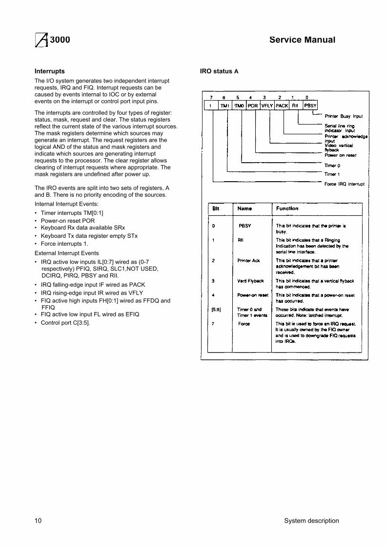
InterruptsThe I/O system generates two independent interrupt requests, IRQ and FIQ. Interrupt requests can be caused by events internal to IOC or by external events on the interrupt or control port input pins.
The interrupts are controlled by four types of register: status, mask, request and clear. The status registers reflect the current state of the various interrupt sources. The mask registers determine which sources may generate an interrupt. The request registers are the logical AND of the status and mask registers and indicate which sources are generating interrupt requests to the processor. The clear register allows clearing of interrupt requests where appropriate. The mask registers are undefined after power up.
The IRO events are split into two sets of registers, A and B. There is no priority encoding of the sources.Internal Interrupt Events:• Timer interrupts TM[0:1]• Power-on reset POR• Keyboard Rx data available SRx• Keyboard Tx data register empty STx• Force interrupts 1.External Interrupt Events• IRQ active low inputs IL[0:7] wired as (0-7
respectively) PFIQ, SIRQ, SLC1,NOT USED, DCIRQ, PIRQ, PBSY and RII.
• IRQ falling-edge input IF wired as PACK• IRQ rising-edge input IR wired as VFLY• FIQ active high inputs FH[0:1] wired as FFDQ and
FFIQ• FIQ active low input FL wired as EFIQ• Control port C[3:5].
IRO status A
10 System description

3000 Service Manual
IRQ status B Interrupt status FIQ
System description 11

3000 Service Manual
Control portThe control register allows the external control pins C[0:5] to be read and written and the status of the PACK and VFLY inputs to be inspected. The C[0:5] bits manipulate the C[0:5] I/0 port. When read, they reflect the current state of these pins. When written LOW the output pin is driven LOW. These outputs are open-drain, and if programmed HIGH the pin is undriven and may be treated as an input.
On reset all bits in the control register are set to 1.
12 System description

3000 Service Manual
The sound system
The sound system is based on the VIDC stereo sound hardware. External analogue anti-alias filters are used which are optimised for a 20 kHz sample rate. The high quality sound output is available at a 3.5mm stereo jack socket at the rear of the machine which will directlydrive personal stereo headphones or alternatively an amplifier and speakers. Two internal speakers are fitted, to provide stereo audio.
VIDC sound system hardwareVIDC contains an independent sound channel consisting of the following components: A four-word FIFO buffers sixteen 8-bit sound samples with a DMA request issued whenever the last byte is consumed from the FIFO. The sample bytes are read out at a constant sample rate programmed into the 8-bit Audio Frequency Register. This may be programmed to allow samples to be output synchronously at any integer value between 3 and 255 microsecond intervals.
The sample data bytes are treated as sine plus seven-bit logarithmic magnitude and after exponential digital to analogue conversion, de-glitching and sign-bit steering, are output as a current at one of the audio output pins to be integrated and filtered externally.
VIDC also contains a bank of eight stereo image position registers each of three bits. These eight registers are sequenced through at the sample rate with the first register synchronised to the first byte clocked out of the FIFO. Every sample time is divided into eight time slots and the three bit image value programmed for each register is used to pulse width modulate the output amplitude between the LEFT and RIGHT audio current outputs in multiples of time slot subdivisions. This allows the signal to be spatially positioned in one of seven stereo image positions.
MEMC sound system hardwareMEMC provides three internal DMA addressregisters to support Sound buffer output; these control the DMA operations performed following Sound DMA requests from VIDC. The registers allow the physical addresses for the START, PNTR (incremental) and END buffer pointers to a block of data in the lowest half Megabyte of physical RAM to be accessed. These operate as follows: programming a 19-bit address into the PNTR register sets the physical address from which sequential DMA reads will occur (in multiples of four words) and programming the END pointer sets the last physical address of the buffer. Whenever the PNTR register increments up to this END value the address programmed into the START register is automatically written into the PNTR register for the DMA to continue with a new sample buffer in
memory. A Sound Buffer Interrupt (SIRQ) signal is generated when the reload operation occurs which is processed by IOC as a maskable interrupt (IRQ) source.
The Memory Controller also includes a sound channel enable/disable signal. Because this enable/disable control signal is not synchronised to the sound sampling requests will normally be disabled after the waveforms which are being synthesised have been programmed to decay to zero amplitude; the last value loaded into the Audio data latch in the VIDC will be output to each of the Stereo image positions at the current Audio Sample rate.
IOC sound system hardwareIOC provides a programmed output control signal which is used to turn the internal speaker on or off, as well as an interrupt enable/status/reset register interface for the Sound Start Buffer reload signal generated by MEMC.
The internal speakers may be muted by the control line SMUTE which is driven from the IOC output C5. On reset this signal will be taken high and the internal speakers will be muted.
The stereo output to the headphone socket is not muted by SMUTE and will always reflect the current output of the DAC channels.
System description 13

3000 Service Manual
The keyboard and mouseThe Keyboard and mouse connection to the ARM is via a keyboard controller and a serial link to the IOC. The ARM reads and writes to the KART registers in the IOC. The protocol is essentially half duplex, so in normal operation the keyboard controller will not send a second byte until it has received an ACK. The only exception to this is during the reset protocol used to synchronise the handshaking, where each side is expecting specific responses from the other, and will not respond further until it has those.
In addition to this simple handshaking system, the keyboard controller will not send mouse data unless specifically allowed to, as indicated by Ack Mouse, which allows the transmission of one set ofaccumulated mouse coordinate changes, or the next move made by the mouse. While it is not allowed to send mouse changes the keyboard controller will buffer mouse changes.A similar handshake exists on key changes,transmitted as key up and key down, and enabled by Ack Scan. At the end of a keyboard packet (two bytes) the operating system will perform an Ack Scan as there is no protocol for re-enabling later. Mouse data may be requested later by means of Request Mouse Position (ROMP).
Key codesThe keyboard controller identifies each key by its row and column address in the keyboard matrix. Row and column codes are appended to the key up or down prefix to form the complete key code.
For example, Q key down — the complete row code is
11000010 (C2 hex) and the column code is 11000111 (C7 hex).Note: Eight keys have N key roll over. The operating system is responsible for implementing two-key roll-over, therefore the keyboard controller transmits all key changes (when enabled). The keyboard controller does not operate any auto-repeat; only one down code is sent, at the start of the key down period.
Data protocolData transmissions from the keyboard are either one or two bytes in length. Each byte sent by the keyboard controller is individually acknowledged. The keyboard controller will not transmit a byte until the previous byte has been acknowledged, unless it is the HRST code indicating that a power on or user reset occurred or that a protocol error occurred; see below.
Reset protocolThe keyboard controller restarts when it receives a HardReSeT (HRST) code from the ARM. To initiate a restart the keyboard controller sends a HRST code to the ARM, which will then send back HRST to command a restart.
The keyboard controller sends HRST to the ARM if :• A power-on reset occurs• A user reset occurs• A protocol error is detected.After sending HRST, the keyboard controller waits for a HRST code. Any non HRST code received causes the keyboard controller to resend HRST.
The pseudo program below illustrates the reset sequence or protocol:
START reset
ON error Send HRST code to ARM then wait for code from ARM.IF code - HRST THEN restart ELSE errorON restart clear mouse position counters
set mouse mode to data only in response to an RMPS request.stop key matrix scanning and set key flags to upsend HRST code to ARM
Wait for next code
IF code - RAK1 THEN send RAK1 to ARM ELSE errorWait for next codeIF code - RAK2 THEN send RAK2 to ARM ELSE error
Wait for next codeIF code SMAK THEN mouse mode to send if not zero and enable key scanELSE IF code - SACK THEN enable key scanningELSE IF code - MACK THEN set mouse mode to send when not zeroELSE IF code NACK THEN do nothing ELSE errorEND reset
Reset sequencingDirection Code Expected Action on Action on Action if
reply wrong reply timeout unexpected(Sender) (Sender) (Receiver)
ARM -> kb Hard reset Hard reset Resend Resend Hard resetKb -> ARM Hard reset Reset Ack 1 Resend Nothing Hard resetARM -> Kb Reset Ack 1 Reset Ack 1 Hard reset Hard reset Hard resetKb -> ARM Reset Ack 1 Reset Ack 2 Nothing Nothing Hard resetARM -> Kb Reset Ack 2 Reset Ack 2 Hard reset Hard reset Hard reset
14 System description

3000 Service Manual
Note, the on/off state of the LEDs does not change across a reset event, hence the LED state is not defined at power on. The ARM is always responsible for selecting the LED status. After the resetsequence, key scanning will only be enabled if a scan enable acknowledged (SACK or SMAK) was received from the ARM.
Data transmissionWhen enabled for scanning, the keyboard controller informs the ARM of any new key down or new key up by sending a two byte code incorporating the key row and column addresses. The first byte gives the row and is acknowledged by a byte acknowledge (BACK) code from the ARM. If BACK was not the acknowledge code then the error process (ON error) is entered. If the BACK code was received the keyboard controller sends the column information and waits for an acknowledge. If either a NACK, SACK, MACK or SMAK acknowledge code is received, the keyboard controller continues by processing the ACK type and selecting the mouse and scan modes implied. If the character received as the second byte acknowledge was not one of NACK/MACK/SACK/SMAK then the error process is entered.
Mouse dataMouse data is sent by the keyboard controller if requested by a ROMP request from the ARM or if a SMAK or MACK have enabled transmission of nonzero values. Two bytes are used for mouse position data. Byte one encodes the accumulated movement along the X axis while byte two gives Y axis movement.
Code values
Both X and Y counts must be transferred to temporary registers when data transmission is triggered, so that accumulation of further mouse movement can occur. The X and Y counters are cleared upon each transfer to the transmit holding registers. Therefore, the count values are relative to the last values sent. The ARM acknowledges the first byte (Xcount) with a BACK code and the second byte (Ycount) with any of NACK/MACK/SACK/SMAK. A protocol failure causes the keyboard controller to enter the error process (ON error).
When transmission of non-zero mouse data is enabled, the keyboard controller gives key data transmission priority over mouse data except when the mouse counter over/underflows.
Acknowledge codesThere are seven acknowledge codes which may be sent by the ARM. RAK1 and RAK2 are used during the reset sequence. BACK is the acknowledge to the first byte of a two byte keyboard data set. The four remaining types, NACK/MACK/SACK and SMAK, acknowledge the final byte of a data set. NACK disables key scanning and therefore key up/down data transmission as well as setting the mouse mode to send data only on ROMP request. SACK enables key scanning and key data transmission but disables unsolicited mouse data. MACK disables key scanning and keydata transmission and enables the transmission of mouse count values it either X or Y counts are non-zero. SMAK enables key scanningand both key and mouse data transmission. It combines
Mnemonic msb lsb CommentsHRST 1111 1111 One byte command, keyboard resetRAK1 1111 1110 One byte response in reset protocolRAK2 1111 1101 One byte response in reset protocolRQPD 0100 xxxx One byte from ARM, encodes four bits of dataPDAT 1110 xxxx One byte from keyboard, echoes four data bits of RQPDRQID 0010 0000 One byte ARM request for keyboard IDKBID 10xx xxxx One byte from keyboard encoding keyboard IDKDDA 1100 xxxx New key down data. Encoded Row (1st byte) and column (2nd byte)
numbersKUDA 1101 xxxx Encoded Row (1st byte) and column (2nd byte) numbers for a new key upRQMP 0010 0010 One byte ARM request for mouse dataMDAT Oxxx xxxx Encoded mouse count, X (byte1) then Y (byte2). Only from ARM to
keyboardBACK 0011 1111 Ack for first keyboard data byte pairNACK 0011 0000 Last data byte ack, selects scan/mouse modeSACK 0011 0001 Last data byte ackMACK 0011 0010 Last data byte ackSMAK 0011 0011 Last data byte ackLEDS 0000 Oxxx Bit flag to turn LED(s) on/offPRST 0010 0001 From ARM, one byte command, does nothing
x is a data bit in the Code; e.g. xxxx is a four bit data field
System description 15

3000 Service Manual
the enable function of SACK and MACK.While key scanning is suspended (after NACK or MACK) any new key depression is ignored and will not result in a key down transmission unless the key remains down after scanning resumes following a SACK or SMAK. Similarly a key release is ignored while scanning is off.
Commands may be received at any time. Therefore, commands can be interleaved with acknowledge replies from the ARM. For example, keyboard sends KDDA (1st byte), keyboard receives command, keyboard receives BACK, keyboard sends KDDA (2nd byte), keyboard receives command, keyboard receives SMACK. If the HRST command is received, the keyboard immediately enters the restart sequence, (ON restart). The LEDS and PRST commands may be acted on immediately. Commands which require a response are held pending until the current data protocol is complete. Repeated commands only require a single response from the keyboard.
ARM commands
Mnemonic FunctionHRST Reset keyboardLEDS Turns key cap LEDs on/off. A three bit field
indicates which state the LEDs should bein. Logic 1 is ON, logic 0 (zero) OFF.DO controls CAPS LOCKD1 controls NUM LOCKD2 controls SCROLL LOCK
RQM Request mouse position (X,Y counts)RQID Request keyboard identification code. The
computer is manufactured with a 6 bit codeto identify the keyboard type to the ARM.Upon receipt of ROID the keyboardcontroller transmits KBID to the ARM
PRST Reserved for future use, the keyboardcontroller ignores this command
RQPD For future use. The keyboard controllerwill encode the four data bits into the PDATcode data field and then send PDAT to theARM.
Mouse interface
The mouse interface has three switch sense inputs and two quadrature encoded movement signals for each of the X axis and Y axis directions. Mouse key operations are debounced and then reported to the ARM using the Acorn key up / key down protocol. The mouse keys are allocated unused row and column codes within the main key matrix.
Switch 1 (left) Row code - 7 Column code -0Switch 2 (middle Row code - 7 Column code - 1Switch 3 (right) Row code - 7 Column code - 2
For example, switch 1 release would give 11010111 (D7 hex) as the complete row code, followed by 11010000 (DO hex) for the column code.
Note: Mouse keys are disabled by NACK and MACK acknowledge codes, and are only enabled by SACK and SMAK codes, ie they behave in the same way as the keyboard keys.
The mouse is powered from the computer 5 V supply and may consume up to 100 mA.
Movement signals
Each axis of movement is independently encoded in two quadrature signals. The two signals are labelled REFerence and DIRection (e.g. X REF and X DIR). The table below defines the absolute direction of movement. Circuitry in the keyboard decodes the quadrature signals and maintains a signed 7 bit count for each axis of mouse movement.
Ink alState
NextState
REF DIR REF DIR
1 1 1 01 0 0 0 Increase count by one0 0 0 1 for each change of state.0 1 1 1
1 1 0 10 1 0 0 Decrease count by one0 0 1 0 for each change of state.1 0 1 1
When count overflow or underflow occurs on either axis both X and Y axis counts lock and ignore further mouse movement until the current data has been sent to the ARM.
Overflow occurs when a counter holds its maximum positive count (0111111 binary). Underflow occurs when a counter holds its maximum negative count (1000000 binary).
16 System description

3000 Service Manual
Keyswitch mapping
KeySize
KeyName
Rowcode
Col.code
Notes
1 Esc 0 0 11 F1 0 1 21 F2 0 2 21 F3 0 3 21 F4 0 4 21 F5 0 5 21 F6 0 6 21 F7 0 7 21 F8 0 8 21 F9 0 9 21 F10 0 A 21 F11 0 B 21 F12 0 C 21 Print 0 D 1,31 Scroll 0 E 11 Break 0 F 1
1 - 1 01 1 1 11 2 1 21 3 1 31 4 1 41 5 1 51 6 1 61 7 1 71 8 1 81 9 1 91 0 1 A1 -_ 1 B1 =+ 1 C1 £ 1 D1 Backspc 1 E 11 Insert 1 F 11 Home 2 0 1,31 Pgup 2 1 11 Numlock2 2 1,41 / 2 3 11 * 2 4 11 # 2 5 1
KeySize
KeyName
Rowcode
Col.code
Notes
1.5 Tab 2 6 11 Q 2 71 W 2 81 E 2 91 R 2 A1 T 2 B1 Y 2 C1 U 2 D1 I 2 E1 O 2 F1 P 3 01 [{ 3 11 ]} 3 21.5 \ 3 31 Delete 3 4 11 Copy 3 5 11 Pgdwn 3 6 11 7 3 71 8 3 81 9 3 91 - 3 A 1
1.75 Ctrl 3 B 1,31 A 3 C1 S 3 D1 D 3 E1 F 3 F1 G 4 01 H 4 11 J 4 21 K 4 31 L 4 41 ;: 4 51 ,* 4 6 •2.25 return 4 7 11 4 4 81 5 4 91 6 4 A1 + 4 B 1
Row and column codes are in Hexadecimal.Notes: 1 Key colour - dark grey
2 Key colour - red3 Key position with N key roll over.4 Green light emitting diode under key cap.
S y s t e m description 1 7

3000 Service Manual
KeySize
KeyName
Rowcode
Col.code
Notes
2.25 shift 4 C 1,31 Z 4 E1 X 4 F1 C 5 01 V 5 11 B 5 21 N 5 31 M 5 41 ,< 5 51 .> 5 61 /? 5 72.75 shift 5 8 1,31 crsrUp 5 9 11 1 5 A1 2 5 B1 3 5 C
1.5 Caps 5 D 1,41.5 Alt 5 E 1,37.0 Space 5 F1.5 Alt 6 0 1,31.5 Ctrl 6 1 1,31 crsrLt 6 2 11 crsrDn 6 3 11 crsrRt 6 4 12.0 0 6 51 6 62.0 Enter 6 7 1
Row and column codes are in Hexadecimal.Notes: 1 Key colour - dark grey
2 Key colour - red3 Key position with N key roll over.4 Green light emitting diode under key cap.
18 System description
3000 Service Manual
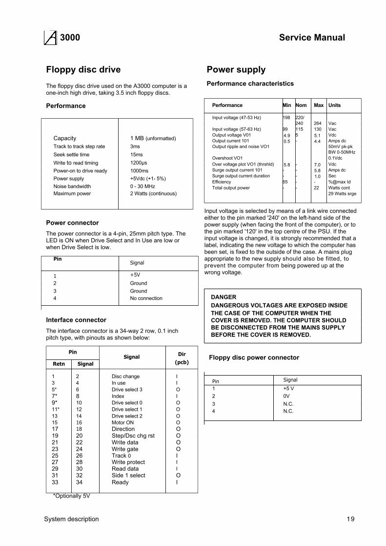
Floppy disc driveThe floppy disc drive used on the A3000 computer is a one-inch high drive, taking 3.5 inch floppy discs.
Performance
Capacity 1 MB (unformatted)Track to track step rate 3msSeek settle time 15msWrite to read timing 1200µsPower-on to drive ready 1000msPower supply +5Vdc (+1- 5%)Noise bandwidth 0 - 30 MHzMaximum power 2 Watts (continuous)
Power connectorThe power connector is a 4-pin, 25mm pitch type. The LED is ON when Drive Select and In Use are low or when Drive Select is low.
PinSignal
1 +5V
2 Ground3 Ground4 No connection
Interface connectorThe interface connector is a 34-way 2 row, 0.1 inch pitch type, with pinouts as shown below:
PinSignal Dir
(pcb)Retn Signal
1 2 Disc change I3 4 In use I5* 6 Drive select 3 O7* 8 Index I9* 10 Drive select 0 O11* 12 Drive select 1 O13 14 Drive select 2 O15 16 Motor ON O17 18 Direction O19 20 Step/Dsc chg rst O21 22 Write data O23 24 Write gate O25 26 Track 0 I27 28 Write protect I29 30 Read data I31 32 Side 1 select O33 34 Ready I
*Optionally 5V
Power supplyPerformance characteristics
Performance Min Nom Max Units
Input voltage (47-53 Hz) 198 220/240 264 Vac
Input voltage (57-63 Hz) 99 115 130 VacOutput voltage V01 4.9 5 5.1 VdcOutput current 101 0.5 - 4.4 Amps dcOutput ripple and noise VO1 50mV pk-pk
BW 0-50MHzOvershoot VO1 0.1VdcOver voltage plot VO1 (thrshld) 5.8 - 7.0 VdcSurge output current 101 - - 5.8 Amps dcSurge output current duration - - 1.0 SecEfficiency 65 - - %@max IdTotal output power - - 22 Watts cont
29 Watts srge
Input voltage is selected by means of a link wire connected either to the pin marked '240' on the left-hand side of the power supply (when facing the front of the computer), or to the pin marked '120' in the top centre of the PSU. If the input voltage is changed, it is strongly recommended that a label, indicating the new voltage to which the computer has been set, is fixed to the outside of the case. A mains plug appropriate to the new supply should also be fitted, to prevent the computer from being powered up at the wrong voltage.
DANGERDANGEROUS VOLTAGES ARE EXPOSED INSIDETHE CASE OF THE COMPUTER WHEN THECOVER IS REMOVED. THE COMPUTER SHOULDBE DISCONNECTED FROM THE MAINS SUPPLYBEFORE THE COVER IS REMOVED.
Floppy disc power connector
Pin Signal
1 +5 V2 0V3 N.C.4 N.C.
System description 19

3000 Service Manual
LinksLink Fitted Effect Default
LK22 Yes
Connection point forleft channel audiospeaker. P1 0V, P2 signal.
None
LK23 YesConnection point forright channel audiospeaker. P1 0V, P2 signal.
None
LK5 No Connection point for anexternal battery. (Only usedif supply of on board NiCadbecomes a problem.)
None
LK20 YesUsed in conjunction with LK19to select size of ROM devices.
Shunt 2-3
LK19 YesUsed in conjunction with LK20to select size of ROM devices.
Shunt 2-3ie 1M
ROM LK19 LK20512K 2-3 2-31M 2-3 2-32M 1-2 2-34M 1-2 1-2
LK25 YesUsed to configure P5 of SK14(RGB Video Socket) to beeither 'VSync' or 'Mode'.
Shunt NFie 'Mode'
Fit shunt for 'VSync'NF shunt for 'Mode'(Mode is required by someSCART TVs.)
LK24 YesUsed to configure P4 of SK14(RGB Video Socket) to beeither 'HSync' or 'CSync'.
Shunt 2-3ie 'CSync'
Shunt , 1-2 for 'HSync'Shunt , 2-3 for 'CSync'
LK27 Yes Used to invert 'VSync'. Shunt NFie 'VSync'
Shunt fitted , VSync*Shunt NF, VSync
LK26 Yes Used to invert 'HSync'. Shunt NFie 'HSync'
Shunt fitted , HSync*Shunt NF, HSync
LK7 No Test point for Non VolatileMemory clock frequency.P1 OV NoneP2 32.768KHz
LK30 Not Used in conjunction with LK29and LK28 (&. 31 on Iss1) toprovide the necessary signalsfor a Genlock interface circuit.P1 VS* NoneP2 HS*
LK28 Not P1 Ckvidc Trk 1-2P2 Clksys* (Shunt
on Iss1)
LK29 Not P1 0V Trk 1-2P2 Sink (Shunt
on Iss 1 )
LK31 Not P1 'Sup' NoneP2 0V
LK6 No Test point for Non Volatile NoneMemory battery voltage.P1 0VP2 1.2V +/- 0.2V
Link Fitted Effect Default
LK8 NoLK9 NoLK10 No Used to set nationality id of LK12 TrkLK11 No the keyboard. ie UKLK12 NoLK13 No
LK1 No Used to optionally link 0V to NF
LK2 No the RFI Shield (Earth). NFLK3 No
Connection point for a designbackup, self containedkeyboard.
NF
P1 Krst * Keyboard resetP2 NCP3 0VP4 5VP5 Krx' From keyboardPS K u ' To keyboard
LK4 NoConnection point for designbackup, mouse to keyboardlink.
NF
P1 Xr X ref P5 Sw(1) Switch 1P2 Xd X dir P6 Sw(2) Switch 2P3 Yr Yref P7 Sw(3) Switch 3P4 Yd Ydir P8 0V
LK17 N o t Used in conjunction with LK18 .to select ROM device type. Trk 1-2
(Shunton Iss1)
LK18 Not Used in conjunction with LK17to select ROM device type.
Trk 1-2ie NonJEDEC
ROM LK17 LK18512K EPROM 1-2 1-2
(Shunton Iss1)
Non JEDEC 1 M ROM 1-2 1-2Non JEDEC 1M EPROM 1-2 1-2JEDEC 1/214M ROM/
EPROM 1 — 12 — 2
LK16 No Used to select the designbackup keyboard. See LK3.
Trk 2-3ieMain K/B
1-2 Selects backup keyboard2-3 Selects main keyboard
LK21 NoSelects the +5V power feed tothe floppy disc drive to be viathe data cable or by separatefeed with PLS.
Trk 2-3ie not viadata cable
1-2 +5V via data cable2-3 +5V via separate cable
LK14 No Used in conjunction with LK15 Trk 1-2LK15 No to select the keyboard uC
device type.Trk 1-2ie NMOS
Device Type LK14 LK158051 (NMOS) 1-2 1-280051 (CMOS) O/C 2-3
LK32 No Provides access to RGB inter-face signals (Issue 1 only):
NF
1 - Red 4 - I-VCSYNCH2 - Green 5 - VSYNC/MODE3 - Blue 6 - 0V
Notes: NF - Not FittedP1 - Pin 10/C - Open CircuitTrk - Tracked
** Active lowt Fitted on Issue 1 PCB
20 System description
3000 Service Manual
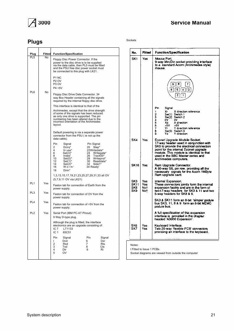
Plugs
Plug Fitted Function/SpecificationPL5 No
Floppy Disc Power Connector. If thepower to the disc drive is to be suppliedvia the data cable, then PL5 must be fittedand the PSU free disc power socket mustbe connected to this plug with LK21.
P1 NCP2 OVP3 OVP4 +5V
PL6 NoFloppy Disc Drive Data Connector. 34way Box Header containing all the signalsrequired by the internal floppy disc drive.
This interface is identical to that of theArchimedes, except that the drive strengthof some of the signals has been reducedas only one drive is supported. The pinnumbering has been altered due to theincorrect orientation of the Archimedeslayout.
Default powering is via a separate powerconnector from the PSU ( ie not up thedata cable).
Pin Signal Pin Signal2 Dcirq* 20 Step*4 In use* 22Writedata*6 Sel(3)* 24 Writegate*8 Index' 26 Track00*10 Sel(0)* 28 Writeprot*12 Sel(1)* 30 Readdata*14 Sel(2)* 32 Side1*16 W o r m ' 34 Ready'18 Dirin*
1,3,13,15,17,19,21,23,25,27,29,31,33 all OV(5,7,9,11 OV via LK21)
PL1 YesFaston tab for connection of Earth from thepower supply.
PL3 Yes Faston tab for connection of OV from thepower supply.
PL4 YesFaston tab for connection of +5V from thepower supply.
PL2 Yes Serial Port (IBM PC-AT Pinout)9 Way D-type plug.
Although the plug is fitted, the interfaceelectronics are an upgrade consisting of:IC 7 LT1133IC 1 65C51
Pin Signal Pin SignalI Dcd 6 Dsr2 Rxd 7 Rts3 Txd 8 Cts4 Dtr 9 Ri5 OV
Sockets
Notes:t Fitted to Issue 1 PCBsSocket diagrams are viewed from outside the computer
System description 21

3000 Service Manual
Sockets (contd)
22 System description

3000 Service Manual
Changes between Issue A and Issue 1 PCBsThis manual covers A3000s produced with both Issue A and Issue 1 PCBs, and drawings for both versions are included. This section summarises the changes made during the production of Issue A boards, and the design changes made for Issue 1.
Modifications to Issue A PCBsComponent value changesThe chart below summarises the component value changes made during the production of Issue A PCBs, showing the first serial number changed.
(Unless otherwise stated, resistors are 5% SMD.)
Comp. Issue A Changed to Serial no.
R67 68R 22R 1000051R68 68R 22R 1000051R69 68R 22R 1000051R70 68R 22R 1000051R71 68R 22R 1000051R81 33K 3K3 1000013R82 150K 1% 22K 1% 1000013R85 33K 3K3 1000013R86 150K 1% 22K 1% 1000013R88 33K 3K3 1000013R89 33K 3K3 1000013R91 150K 1% 22K 1% 1000013R92 33K 3K3 1000013R93 150K 1% 22K 1% 1000013R95 150K 1% 22K 1% 1000013R97 150K 1% 22K 1% 1000013R98 150K 1% 22K 1% 1000013R99 150K 1% 22K 1% 1000013R101 33K 3K3 1000013R105 470R 680R 1000051R129 33R 22R 1000051R130 33R 22R 1000051R131 33R 22R 1000051R132 33R 22R 1000051R133 33R 22R 1000051R137 100K 10K 1000051R502 6K8 4K7 1000013R530 22K 1K 1004150C75 100p CPLT 2n2 CPLT 10% 1000013C77 2n7 CPLT 22n MPSTR 10% 1000013C80 22n MPSTR 100n MPSTR 10% 1000013C81 330p 2n2 CPLT 1000013C82 330p 2n2 CPLT 1000013C86 330p 2n2 CPLT 1000013C88 22n MPSTR 100n MPSTR 10% 1000013C90 100p CPLT 2n2 CPLT 10% 1000013C91 330p 2n2 CPLT 1000013C92 2n7 CPLT 22n MPSTR 10% 1000013
The following additional modifications were made during the production of Issue A PCBs:
Serial interface10K resistor (5%, conventional type) was added as a 'pullup' to the rear of the PCB, connected between the signal Rii* (IC7 pin 18) and +5V (from serial number 1000001).
Video genlockingThe tracks on the underside of the PCB, between the pins of both LK28 and LK29, were cut. 2-pin wafers were fitted to LK28, 29 & 30, and shunts to LK28 and 29 (but not LK30) (from 1000251).
I2C-bus accessTwo 5-way headers (0800,486) were fitted to SK8 and SK9 (from 1000251).
JEDEC & non-JEDEC EPROMsTo permit the use of JEDEC and non-JEDECEPROMs, tracks on the PCB, between the pins ofboth LK17 and LK18, were cut. 2-pin wafers were fitted to LK17 & 18, and shunts fitted to LK17 and 18 (from 1000251).
Fixing of 64W connectorTwo rivets (Avdel 11070312) were added to the mounting holes of the 64-way expansion connector.
Design changes made between Issue A and Issue 1 PCBs
Serial interfaceThe 'strapped on' resistor (see above) was replaced by a permanent resistor (10K SMD 5%) — R144.
Signal conditioningR141, R142 and R143 have been added (22R SMD 5%) to REF8M, RA9 and IORQ. R134 has been moved to accomodate these.
A capacitor C116 (2n7) has been added between SW3 and OV.
Video genlockingLK28 & 29 tracks have been deleted (see above). LK 28, 29 & 30 moved.LK31 has been added. This allows access to the VIDC supremacy bit (pin 28) and GND.
JEDEC & non-JEDEC EPROMsThe tracks between the pins of LK17 & 18 have beendeleted (see above).
System description 23

3000 Service Manual
RGB & SYNCA 6-way connector (LK32, not fitted) has been added to RGB & SYNC for internal access.
Production changesThe components R550, C55, C78, C500, C501 and C504 have been moved to facilitate production.
R145 (4K7 SMD 5%) has been added between 1C2 pin 31 and +5V to accomodate ATE.
Test points have been added to the following lines:ARM20-MEMC3MEMC38 MEMC39 MEMC40 MEMC41 MEMC42(R129-R132 have been moved to accomodate thesetest points.)
24 System description

3000 Service Manual
A3000 expansionInternal expansion
DANGERDANGEROUS VOLTAGES ARE EXPOSED INSIDETHE CASE OF THE COMPUTER WHEN THECOVER IS REMOVED. THE COMPUTER SHOULDBE DISCONNECTED FROM THE MAINS SUPPLYBEFORE THE COVER IS REMOVED.
The following internal upgrades are currently available for the A3000 computer:• User port / MIDI internal expansion card• 1 Mb Ram upgrade• Serial port• Econet moduleInternal upgrades must be fitted by an Acorn Dealer or Approved Service Centre.
InterfaceThe electrical signals available on the internal expansion are a subset of those described in 'A Series podules', available from Acorn Customer Service as an Application Note, or on the SID system (Doc Ref 0310101).
The connection is via two 17-way 0.1 inch pitch connectors and two 5-way 0.1 inch connectors (the latter fitted as standard to Issue 1 PCBs and later). Expansion cards should use 0.025 in square pin headers.
Expansion bus connectors
Pin no SK3 SK11 SK8 SK91 +5V 0V C[0] 0v2 PWE* +5v C[1] REF8M3 PS1* PRE* BI PFIQ*4 CLK2 PR/nW IORQ* Ms[1]*5 LA[2] LA[4] IOGT +5V6 LA[3] LA[5]7 BD[0] LA[6]8 BD[1] LA[7]9 BD[2] 0V10 BD[3] LA[8]11 BD[4] LA[9]12 BD[5] LA[10]13 BD[6) LA[11]14 BD[7] LA[12]15 RST* LA[13]16 0V PIRQ*17 +5V 0V
Note: Pin 1 is at the righthand end when viewed from thefront of the computer.
The interface is configured as 'Podule 1, Module 1'.
It is recommended that the load on each signal does no exceed 3HCT gates or that stated in 'A Seriespodules'. Any upgrade must be able to drive at least 7 HCT and 3 TTL loads on the data bus.
Power supplyThe maximum power available from the +5V rail is 600 mA. The maximum dissipation inside the case is 0.5W (100mA).
MechanicalThe rear panel required is shown in the drawing at the back of this manual. The size of the User Port/MIDI expansion card PCB and position of the connectors are also shown in the drawing at the back of the manual.
User port/MIDI expansion card (UPM)
IntroductionThe A3000 User Port / MIDI expansion card fits inside the computer, and provides:• An 8-bit User Port, largely compatible with the User
Port interface on the BBC Model B and Master 128 microcomputers (and with the User Port on the Archimedes I/O expansion card).
MIDI (Musical Instrument Digital Interface), with IN, OUT and THRU connections, compatible with the International MIDI Association specification.
Main components• 65C22 VIA for the User Port• 2691 UART for the MIDI• 27128 EPROM containing firmware and ID byte.
A3000 expansion 25

3000 Service Manual
UPM block diagram
Comparison with Archimedes expansion cardsARCHIMEDES I/O EXPANSION CARD• The VIA is at the same address and clocked at the
same speed. Port A PA<0..2.> is used to page ROM. These are the same as the UPM when set for 2764/27128.
• The User port is the same (Port B). The VIA interrupts go through a link, which is not normally fitted.
• The MIDI section is not the same.• The ADC and 1 MHz bus are not fitted to the UPM.
MIDI EXPANSION CARD• The UART is the same (Signetics 2691), but is at a
different address (see below).• The ROM page latch is not the same.
LA13 LAl2 offset address
MiDi PoduleUPM upgrade
11
01
8200083000
Addresses of main system components
Address Component
&0000-1FFC ROM/EPROM 271 28 as standard (16k x8 bit). Larger EPROMS can be fitted ifthe links marked X are cut between pins1 & 2, and relinked 2 to 3.Eprom size LK 1 LK 2 LK3 LK427642712827256 X27512 X X1M bit (JEDEC) X X2m bit X X X4m bit X X X X
Contains the iD byte 63 (dec).The start-up information must be at thetop of the ROM.
&2000-2FFC VIA 65C22 - 2Mhz part.
Port A PA<7..0> used to page the ROM.
CAs Not Used.
Port B PB<7..0>, CB1 and CB2 for the
User Port.
Use 2Mhz synchronous cycle to accessthe VIA.
The interrupt output connects directly to
PIRQ*.
No User Port interrupt handler provided.&3000-3FFC UART 2691 - For the MiDi interface.
26 A3000 expansion

3000 Service Manual
Fitting an Internal expansion cardThis procedure covers the fitting of an internal expansion card, such as the User Port / MIDI expansion card. This work should only be carried by Acorn Dealers or Approved Service Centres:1 Follow the procedure for removing the cover of the
computer given in the next chapter.2 Unscrew the two machine screws holding the rear
blanking plate in place, and remove the plate:
3 Plug the expansion card into the connectors on the PCB, and press firmly home:
4 Replace the two screws holding the expansion card backplate, and secure firmly.
5 Replace the cover of the computer.6 Run the dealer test software to test the correct
function of the computer and the upgrade, and of any other upgrades fitted.
Keep the rear panel blanking plate with the computer, in case the expansion card is removed later.
1Mb RAM upgrade
The A3000 computer RAM can be upgraded from 1Mb to 2 Mb by the addition of a 1Mb RAM module which plugs into the main PCB.
Fitting a RAM upgrade1 Follow the procedures detailed in the next chapter
for the removal of the computer cover and the keyboard.
2 To fit earlier RAM upgrades with securing lugs, remove two PCB retaining screws and plug the upgrade module, in a vertical position, into the board. Later upgrades, with no fitting lugs, simply push into the connectors on the PCB:
3 Replace the screws securing the PCB and the upgrade module.
4 Replace the keyboard and the cover of the computer.
5 Run the dealer test software to test the correct function of the computer and the upgrade, and of any other upgrades fitted.
A3000 expansion 27

3000 Service Manual
Serial port upgradeIntroductionThe A3000 computer is fitted with a 9-way D-type serial connector on the back panel, but this is not functional until a serial port upgrade kit has been fitted by an Acorn Dealer or Approved Service Centre. Only Acorn Serial Port Upgrade kits should be used.
The A3000 serial port upgrade consists of a serial processor chip and a line driver chip, which fit into existing sockets on the PCB.
Connector pinouts
Fitting the Acorn A3000 serial port upgrade
WARNING: It is a recommended requirement thatanti-static precautions should be utilised at all lev-els of servicing, ie antistatic matting and wrist-straps.
1 Follow the procedures in the next chapter for the removal of the cover and the keyboard.
2 Remove the Econet module and the User Port / MIDI expansion card, if fitted.
3 Insert the 28-pin IC 65C51 into socket IC1, and the 24-pin IC LT1133 into socket IC7. The notched ends of the ICs should face towards the left hand side of the PCB (viewed from the front of the computer) :
4 Fit the serial number label to the PCB near the upgrade ICs.
5 Refit any modules and expansion cards removed in step 2 above, and replace the cover of the computer.
6 Remove the label 'Serial not fitted' from the rear panel.
7 Run the dealer test software to test the correct function of the computer and the serial port, and of any other upgrades d is turbed dur ing th is installation.
28 A3000 expansion
3000 Service Manual
Fitting an Econet module1 Follow the procedure in the next chapter for
removing the cover of the computer.2 Plug the module onto the PCB connectors:
3 Replace the cover of the computer.
4 Run the dealer test software to test the correct function of the computer and the Econet module, and of any other upgrades fitted. Refer to the appropriate Econet file server Manager's Guide for instructions on setting the station id.
External expansion
InterfaceintroductionThe A3000 computer supports an external expansion card (podule) interface, although with some minor differences from other ARM based systems:• Single +5Volt power supply rail, rated at a maximum of
1 Amp (no +12 or –5 Volt rails provided)• No support for Co-Processor type cards• The external expansion card is in software slot 0• The podule must be capable of driving 3 TTL and
7HCT loads on the data bus.
Refer to the application note 'A series podules' (referenced at the start of this chapter) for a full podule interface specification.
Physical dimensionsAs the podule is external to the computer enclosure there is no real limit on the size of the unit. Care should be taken not to block off any of the other expansion ports on the rear of the computer.
Fitting an expansion card
WARNINGPower down the computer before fitting or removingan external expansion card. It is anticipated that expansion cards will be fitted into a suitable external expansion card unit. Slots are provided underneath the case of the computer, into which a tongue in the case of the expansion card unit can locate. Tapped holes are provided in the backplate of the computer to enable the expansion unit to be secured to the computer with two M6 screws.
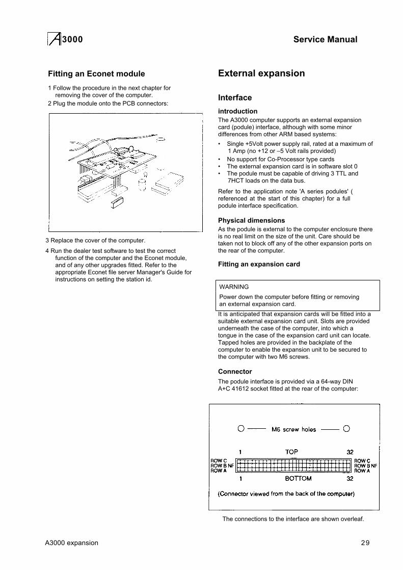
ConnectorThe podule interface is provided via a 64-way DIN A+C 41612 socket fitted at the rear of the computer:
The connections to the interface are shown overleaf.
A3000 expansion 29

3000 Service Manual
External expansion connections
Pin ROW A ROW C Row C description
1 0V 0V Ground2 LA[15] reserved3 LA[14] 0V Ground4 LA[13] 0V Ground5 LA[12] reserved6 LA[11] MS[0]* MEMC Podule select7 LA[10] reserved8 LA[9] reserved9 LA[8] reserved10 LA[7] reserved11 LA[6] reserved12 LA[5] FIST* Reset (see note below)13 LA[4] PR/W* Read/not write14 LA[3] PWE* Write strobe15 LA[2] PRE* Read strobe16 BD[15] PIRQ* Normal interrupt17 BD[14] PFIQ* Fast interrupt18 BD[13] S[6]*19 BD[12] C[1] 12C serial bus clock20 BD[11] C[0] I2C serial bus data21 BD[10] S[7]* External Podule select22 BD[9] PS[0] Simple Podule select23 BD[8] IOGT* MEMC Podule handshake24 BD[7] IORO MEMC Podule request25 BD[6] BL* VO data latch control26 BD[5] 0V Supply27 BD[4] CLK2 2MHz Synchronous clock28 BD[3] CLK8 8MHz Synchronous clock29 BD[2] REF8M 8MHz Reference clock30 BD[1] +5V Supply31 BD[0] reserved32 +5V reserved
Note: The RST* signal is the system reset signal, drivenby IOC on power-up or by the keyboard reset switch. It isan open-collector signal, and expansion cards may driveit also if this is desirable. The pulse width should be atleast 50ms.
30 A3000 expansion

3000 Service Manual
Disassembly and reassembly
DANGERDANGEROUS VOLTAGES ARE EXPOSED INSIDETHE CASE OF THE COMPUTER WHEN THECOVER IS REMOVED. THE COMPUTER SHOULDBE DISCONNECTED FROM THE MAINS SUPPLYBEFORE THE COVER IS REMOVED.
Removing the coverTo remove the cover from the computer, follow this procedure:1 Disconnect all peripherals and unplug the computer
from the mains supply.2 Unplug the mouse connector from the underside of
the computer.3 Remove the centre fixing screw on the underside of
the case:
4 Remove the two screws from the clips at the rear of the computer:
5 Unhook the two clips and slightly lift up the back of the cover, pivoting on the front.
6 Locate the three rectangular holes on the front underside of the case. Insert a screwdriver into the rear edge of each of these holes in turn. Push and twist until the catch comes free of the lower case.
7 Repeat this procedure for the other two holes until the cover lifts clear.
Fitting is the reverse of the above procedure, ignoring step six.
Removing the keyboard
WARNINGThe keyboard connector can be damaged byincorrect handling. Hold it by the white plasticstrengthening strip only. Do not touch the trackfaces or apply pressure to the cable itself.
1 Follow the procedure for removing the cover.2 Unplug the keyboard connector, and lift the
keyboard out from the lower case.Fitting is the reverse of the above procedure.
Removing the floppy disc drive1 Follow the procedure for removing the cover.2 Disconnect the power supply cable from the drive,
and the ribbon cable from the PCB.3 Remove the keyboard (see above).4 Turn the lower case upside down and support the
drive on a foam pad.5 Remove the four recessed drive fixing screws:
Disassembly and reassembly 31

3000 Service Manual
6 Tturn the case back up again. Lift the drive clear. Fitting is the reverse of the above procedure.
Removing the PSU1 Follow the procedures for removing the cover and the
keyboard (above).2 Disconnect the two faston connectors from the PCB, the
connector on the PSU and the power cable to the disc drive.
3 Remove the warning sticker on top of the PSU cover. If the PSU is held in place by a plastic rivet, release the rivet jaws by pushing the pin in the centre of the jaw down, and then push the rivet itself down. If a self-tapping retaining screw is fitted, this should be should be unscrewed. The PSU and its cover will then lift out:
Replacing the PSUWhen replacing the PSU, ensure that the plastic insulating film is replaced underneath the PSU, and that the the cover is correctly located. Take care not to overtighten the self-tapping screws.
Removing the PCB1 Follow the procedures above for the removal of the
cover, the keyboard, floppy disc drive and the 1MByte RAM, if fitted.
2 Remove the power leads at the point where they connect to the PCB (red +5V and black OV).
3 Disconnect the two speaker leads, and remove the RH speaker (viewed from the front).
4 Unscrew the three self-tapping screws retaining the PCB, and the PCB and rear panel will lift out of
the case:
Fitting is the reverse of the above procedure — insert the PCB into the clips at the front edge of the case before lowering into place. Care should taken to ensure that the RESET key is not damaged.
Replacing the batteryThe battery providing current to the real-time clock and battery-backed RAM is soldered to the PCB:
If this needs replacing, it will have to be removed using a soldering iron and a desoldering gun. Repair sites lacking the equipment and experience in this type of work should not attempt to carry it out, or damage to the PCB may result. Care should be taken to avoid shorting the battery — connecting the positive and negative terminals — even on a battery being discarded.
32 Disassembly and reassembly

3000 Service Manual
Fault diagnosis IntroductionThis chapter is a guide to the diagnosis and repair of basic faults in the A3000 computer system.
It consists of algorithms to enable you to trace & remedy faults in a 'dead' computer, followed by instructions for running the functional test software, designed to isolate faults in a computer which is working.
The next chapter 'Main PCB fault diagnosis and repair' is designed to help those repair centres equipped to do so, to diagnose and repair faults at component level on the main PCB.
Test equipment required:• 100 MHz oscilloscope.• DC Voltmeter.• Earth Continuity tester.• Serial port loopback plug (part number 0280,087).
See the Appendix for details of the plug.• 32 ohm impedance headphones.• IC extraction tools.• Antistatic matting and wrist straps.• Standard hand tools.
DANGER
AFTER REFITTING OR FITTING AREPLACEMENT ASSEMBLY, CARRY OUTEARTH CONTINUITY TESTING ON THEASSEMBLED COMPUTER ACCORDING TO THEPROCEDURE GIVEN IN APPENDIX B.
WARNINGS• Repairs to multi-layered PCBs:
The main PCB is a four-layer board.Components should only be removed from theboard using equipment specifically designed forthis purpose. For details of suitable equipmentavailable, contact Acorn Customer Service.
• Repairs to surface-mounted devices:The ARM, MEMC, IOC AND VIDC ICs on theA3000 PCB are surface-mounted components.Do not attempt to remove them from the boardand replace them unless you have theexperience and the correct equipment to do so.
• System clock failure:If the computer is powered on for more than afew seconds and there is no system clock,there is a risk that all four ARM chips may bedamaged, as well as the RAM.
• Faulty MEMC:if MEMC is faulty or the RAS/CAS signals arenot being generated, the RAM may be damagedif the machine is left on too long. If you suspecta fault in these areas, scope the RAS and CASlines for a few seconds in order to make surethat they are still active, then turn the machineoff. Do not leave the computer on for more thana few seconds at a time.
• Antistatic precautions:It is a recommended requirement that anti-staticprecautions should be utilised at all levels ofservicing, ie antistatic matting and wrist-straps.
Fault diagnosis 33

3000 Service Manual
Checking a 'dead' computer
34 Fault diagnosis

3000 Service Manual
Checking the sound system for faultsNote: Both SoundDMA and SoundChannel modules must be active (ie, not unplugged) before starting this test.
*TEST PROGRAM
10 REM > Check all channels
20 VOICES 830 FOR channel-1 TO B40 OSCLI("Channelvoice "+STRS(channel)+" "+STR$(2))50 NEXT60 FOR channel - 1 to 870 SOUND channel, -15, 100,2480 PRINTchannel
90 k-GET
100 NEXT
RUN PROGRAM.PRESS A KEY AND REPEAT EIGHT TIMES. PRiNTS CHANNEL NUMBER TO THE SCREEN AND PLAYS VOICE 2 FOR EACH CHANNEL.
Fault diagnosis 35
3000 Service Manual
• headphones to the 'Headphones 32 ohm' socket• monochrome monitor to the 'MONO VIDEO' socket• analogue RGB monitor to the 'ANALOGUE RGB'
socket• monitors to the mains supply• A3000 computer to the mains supply.
Connecting and disconnecting the power• You must CONNECT the power only when you have
made all the other connections• You must DISCONNECT the power before
removing any other connections.
Validating the test equipmentBefore carrying out any of the tests in this section, validate the test equipment using a known good system. If the test equipment fails, you should repair the test equipment and retest on a known good part.
Before you startBefore the start of each day or testing session, you must first:• Adjust the colour monitor to ensure adequate
contrast and brightness• Inspect all the mechanical parts of the test
equipment and replace any parts as necessary.Also, if required:• Ensure that the printer has sufficient paper• Connect the printer to the mains supply. Do NOT
turn on.
Saving and restoring the CMOS RAMThe tests alter the contents of the battery backed RAM that holds the A3000's configuration data. These must be saved before any of the tests is run, and restored when the last test is over.1 Insert the Test disc into the floppy disc drive.2 Switch on the monitors and computer.3 Type F12 to get to the command line prompt.4 At the RISC OS supervisor prompt (an asterisk)
type the following;DRIVE 0 CMOSLS
5 When prompted, replace the Test disc with an ADFS 800k write enabled disc, the Data disc.
6 Type 'S' to save the contents of the RAM, or 'L' to load a previously saved copy of the RAM.
7 Type the filename to use.8 When prompted, replace the Test disc in the drive
and press the space bar to continue.9 Put the data disc in a safe place. Do NOT use this
disc for the later floppy disc test.10Type 'Q' to quit this option.
Functional tests
Notes:• Please read the following section 'General test
procedure' before you carry out any of the tests.• For details of how to repair the main PCB, see Main
functional test.
IntroductionThe A3000 test disc enables the engineer to test the functionality of the computer and Acorn upgrades, and to isolate any faults which may appear. The functional test cannot of course be run on a 'dead' computer — see the previous section for advice on diagnosing faults in 'dead' computers.
General test procedureThe A3000 computer, mouse, expansion cards, Testdisc, Port Tester assembly and Econet cables aredesigned and specified by Acorn Computers Ltd andmay not be changed without written consent from
Acorn. All items should be complete with the correctcables so that you can connect them to the A3000computer.
Equipment required• A3000 computer to be tested• Mouse• 3.5 inch Test disc, part number 0280,032• Two ADFS 800k 'D' formatted, write enabled, 3.5
inch discs, to be labelled Scratch Disc and Data disc.
• Serial port loopback' plug for A3000 (Acorn part number (0280,087). See the Appendix for details.
• Epson FX80 or Olivetti JP101 printer• Pair of 32 ohm stereo headphones• Mono monitor• Analogue RGB monitor.
Note: You can replace the specified printers with any other manufacturer's direct functional equivalent (in terms of BOTH hardware interface and software).
Removing the top cover of the computer main unitRemove the top cover of the A3000 computer as detailed in the previous chapter 'Disassembly and Assembly'.
Connecting up the equipmentConnect the:• serial port 'Ioopback' plug to the 'SERIAL' socket• printer to the 'PARALLEL PRINTER' port
36 Fault diagnosis

3000 Service Manual
Carrying out the testsThere are two types of tests – subjective and non subjective. The test program passes or fails the equipment on the non-subjective tests; however, you must judge whether the equipment passes or fails the subjective tests. It is a good idea for testers tofamiliarise themselves with the correct results givenby a known good computer. In this way they will be in a better position to judge faulty results.
Performing soak testsAt the successful completion of a main PCB functional test, you should carry out a soak test. To do this, select the relevant option and then insert the scratch disc when prompted. The test runs for 12 hours. When the test is running the Caps Lock and Num Lock LEDs will flash, provided that no error has occurred. If a disc error occurs all the LEDs will be off (see table below); the disc error is also displayed on the screen. If the test is completed without an error then the Scroll Lock LED will flash and the Caps Lock and Num Lock LEDs will be extinguished.
Num Lock Caps Lock Scroll Lock Screen
No errorsErrorFinished
FlashingOffOff
FlashingOffOff
OffOff
Flashing
RunningFail
Pass
WarningDuring the soak test the unit under test should not be subjected to mechanical shock or movement. The unit shall not be turned off unless the test has terminated –the pass or fail message will be displayed.
Safety checkAfter repairing a unit, and after the soak test, you should carry out the earth continuity check mentioned at the start of the chapter, followed by a further run-through of the functional test, in case the earth check causes malfunction in the computer.
Repairing faultsWhen repairing an A3000 computer, you should repair the faults in the order in which they occurred during the test (ie repair the first recorded failure FIRST).
For further information on checking for faults and carrying out repairs, refer to the appropriate section of this manual.
Restoring the CMOS RAMAfter passing the soak test, the unit under test needs to be restored to the customer's configuration. This is carried out by reloading the CMOS RAM from the data disc saved earlier, by selecting the Load/Save CMOS RAMoption from the main menu. Then select the Load option after inserting the Data disc when
prompted. See 'Saving and restoring the CMOS RAM' above for details of the test procedure.
PackingAfter servicing, repack the A3000 computer in its box. To avoid damage, do NOT send the computer through the post or by courier unless it is in its original packaging. The original packaging should be checked for damage to the outer casing and poly inserts.
Fault diagnosis 37

3000 Service Manual
Main computer tests
Running the testRun the main functional test software as follows:Ensure that CMOS RAM contents have been savedto disc by using the Load/Save CMOS RAM option described above. Then restart the system with a delete-power-on. To perform a delete-power-on, do the following: Whilst holding down the <Delete> key, turn the computer on. Note that the <Delete> key needs to be held down for several seconds. The screen should display the DESKTOP environment.
Note: A useful indication of the success of the delete-power-on sequence is the momentary appearance of a red border area on the screen.
Insert the Test disc. Hold down Ctrl, Shift and *, then press Break. The program will load from disc.The 'Dealer Test Menu' is displayed:
1
2
34
5
A3000 Dealer Test Menu
Main ComputerUpgradesLoad/Save CMOS RAMSoak Test
QuitSELECT OPTION :
Machine identification testSelect the option Main computer.
After selecting and loading the required test program, the A3000 computer cycles through a series of tests beginning with the computer type/model test. This test is extremely fast and the type and model number of the computer is displayed immediately:
This computer is a
BBC A3000
CHECK DESCRIPTION
THEN PRESS <SPACE> TO CONTINUE
You should:1 Check that the description displayed on the screen
is correct.2 If Unknown UUT is displayed then there is a memory
fault.
Action If test fallsChange the main PCB, or see the next chapter for
repair.If an RS232 or 1Mb RAM upgrade is fitted but not mentioned, switch off the unit under test, remove the upgrade and then continue the test. When the computer has passed the main test sequence, power down the unit and re-install the upgrade and then run the relevant upgrade test.
If the description is the same, press the space bar to continue to the next test.
Test optionsTEST
OPTIONS
A AllTests Except PrinterB AllTests and Epson PrinterC AllTests and JP101 Printer
SELECTOPTION
Select the test appropriate to the printer fitted. If you do not want to test the printer and do not need a printout of the results, you can select the 'All Tests Except Printer' option.
MemoryThe functional test continues by testing the memory. The screen clears and displays the following messages:
Memory test
Phase one: incrementing pattern ....
Phase two: TRUE hierarchy ............
Phase three: FALSE hierarchy ........
Phase four: Cycling bits ............
PASSED/FAILED messagePress SPACE to continue.
A failed message will end the tests. Action if test fallsChange the main PCB, or run the main memory test in the next chapter, and repair as necessary.If the test has PASSED, press the Space Bar to continue the test.
38 Fault diagnosis

3000 Service Manual
Battery backed RAMThe test continues by testing battery backed RAM. The following message is displayed on the screen:
Battery Backed Ram (BBR) test running.
Reading BBR into main memory.
Checking read/write function of BBR.
Re—loading configuration parameters.
PASSED/FAILED message
PRESS <SPACE> TO CONTINUE
Press the Space Bar to continue the test. Action if test fallsCheck battery and connections, and check battery is charged. Re run the test. if the test still fails, replace the main PCB, or see the NVM and RTC tests in the next chapter, and repair as necessary.
TimeThe functional test continues by testing the time and date settings. A series of options is displayed on the screen:
DO YOU WANT TO ?
1. CHECK THE DATE AND TIME2. SET THE DATE AND TIME3. CHECK THEN SET THE DATE AND TIME
PRESS 1 OR 2 OR 3
The normal procedure is to select option 1. If you want to reset the time or date you would select 2 or 3. For example, you can:
1 Type 1 to check the date and time.2 Check that the time is correct and the seconds are
incrementing correctly.3 To continue with the test, press the Space Bar.
LoudspeakerThe functional test continues by testing the operation of the loudspeakers. A short repeating sequence of four notes is played, first through the left and then the right speaker. The following message is displayed:
LOUDSPEAKER TESTLISTEN AND CHECK SOUND
THEN PRESS <SPACE> TO CONTINUE
You should:1 Listen to the sequence of notes.2 Check that the first four notes come from the left
speaker and the second four from the right.3 Check that the sound produced is correct. This is a
subjective test, so if you detect any deviation, make a note of the fault.
Action if test fallsIf no sound, or sound from one speaker only, then check speaker connections. If it still fails, substitute known good speakers and re-test. If the sound comes from one speaker only check that the headphone plug is inserted correctly. If test still fails, replace the main PCB, or carry out the Audio test in the next chapter, and repair as necessary
To continue with the test, press the space bar.
HeadphonesThe Functional test continues by testing the operation of the headphones. The following message is displayed as the test proceeds:
HEADPHONE TEST RUNNING
LISTEN AND CHECK SOUNDTHEN PRESS <SPACE> TO CONTINUE
The test consists of a repeating sequence of eight musical notes. The first four notes are played on one headphone and the next four notes on the other headphone.
1 Put on the headphones.2 Listen to the sequence of notes.3 This is a subjective test, so if you detect any deviation
in either headphone, note down the fault.
Action if test fallsIf no sound or poor/faulty sound on known good headphones, replace the main PCB, or carry out the Audio test in the next chapter, and repair as necessary. Ensure the headphones are plugged in correctly.
To continue with the test, press the Space Bar.
Standard colour monitorThis test consists of a series of screen displays. You proceed through the test at your own pace.
The first display consists of a series of white lines radiating from the top lefthand corner. A cursor, in the shape of a bird, travels across the screen, starting from the bottom left and finishing at the top right. The features to check are:
• the accuracy of the lines• the movement and integrity of the cursor.
Fault diagnosis 39
3000 Service Manual
This is a subjective test, so make a note of any faults.When you have finished looking at the screen display, press the Space Bar to move to the next display.
The next screen displays consist of four test cards. There is a test card for each of the three colour guns, and a 'grey scale' to test the three guns. The four test cards are:• Red scale• Green scale• Blue scale• Grey scale.Each test card consists of 16 concentric circles beneath a horizontal band which is divided into 16 sections. A pale border highlights the left most eight sections of the band in order to distinguish the band from the background. The whole test card is surrounded by a contrasting border.
The purpose of the cards is to display 16 shades with the shade of the border as the middle of the range. You should observe:• the 16 shades displayed• the mid-coloured border• the quality of the 'grey scale' display• the integrity of each test card.This is a subjective test, so make a note of any faults which you detect and when you are ready to continue press the Space Bar.
Action If test fallsif display rolls or is unstable, perform a Delete Power-on until the correct default value is obtained. The computer may have lost its configuration value for SYNC. Type at the keyboard:
•CON. SYNC 1 (RETURN)
Press RESET and see if if any change occurs. If no improvement is visible, change the main PCB, or perform the Video tests in the next chapter, and repair as necessary.
Keyboard Functional testLEDs
This test checks that the LEDs (Caps Lock, Scroll Lock and Num Lock) are working.
Keys stuckDuring this test, any keys or mouse buttons which are in a permanently closed position (ie stuck down; are displayed on the screen. If any keys are permanently closed, then it will be impossible to continue the test.
If everything is normal and no keys are stuck, then the last key pressed clears the screen and the Test program passes straight on to the next test.
To carry out this test:1 Follow the instructions which appear on the screen.
These tell you when to check that each LED is ON and OFF.
2 Note down any LED failures before continuing the test. These are not recorded.
3 After each set of instructions press Break to move to the next instruction.
MouseThis tests the three buttons on the mouse and the movement of the mouse to the left, right, up and down. Each of the mouse buttons (ie left, middle, right) are displayed on the screen in turn, together with a pointer. You should:
1 Move the mouse, until the pointer is within the box on the screen, then press the button displayed on the screen.
2 The box displayed on the screen should disappear and the next button appear.
If the button cannot be made to disappear then it will be IMPOSSIBLE to continue the test. You should repeat the test with the known good mouse to isolate the fault to either the keyboard or the mouse. Replace faulty components, then retest.
If everything is normal, the program moves on automatically to the next test.
KeysThe screen clears to show a representation of thekeys in the main keyboard area. You need to test each key in turn in the correct order, ie work from the bottom line of the keyboard and from left of the keyboard to the right:
1 Press Caps Lock.2 Check that the picture of the Caps Lock key disappears from the screen.
3 Press Alt and check that the picture of the Alt key disappears from the screen. If the picture of the key does not disappear from the screen then leave a small delay before pressing the next key.
If the screen stops clearing the characters as you press the keys, go back to the lowest, leftmost key remaining on the screen and start again from there.4 Continue working along the bottom line. Then start working from left to right along the next line up.
Note: If you accidentally press two keys together, you will see both keys displayed on the screen. You should press Break to continue.
If the same fault occurs repeatedly or the picture of the depressed key refuses to disappear, then it will be IMPOSSIBLE to continue the test. You should replace the keyboard and start the whole test again.
40 Fault diagnosis
3000 Service Manual
5 When all keys in the main keyboard area have been pressed successfully, the screen clears and displays a diagram of the rest of the keyboard area. Again, press each key in turn, following the guidelines above.
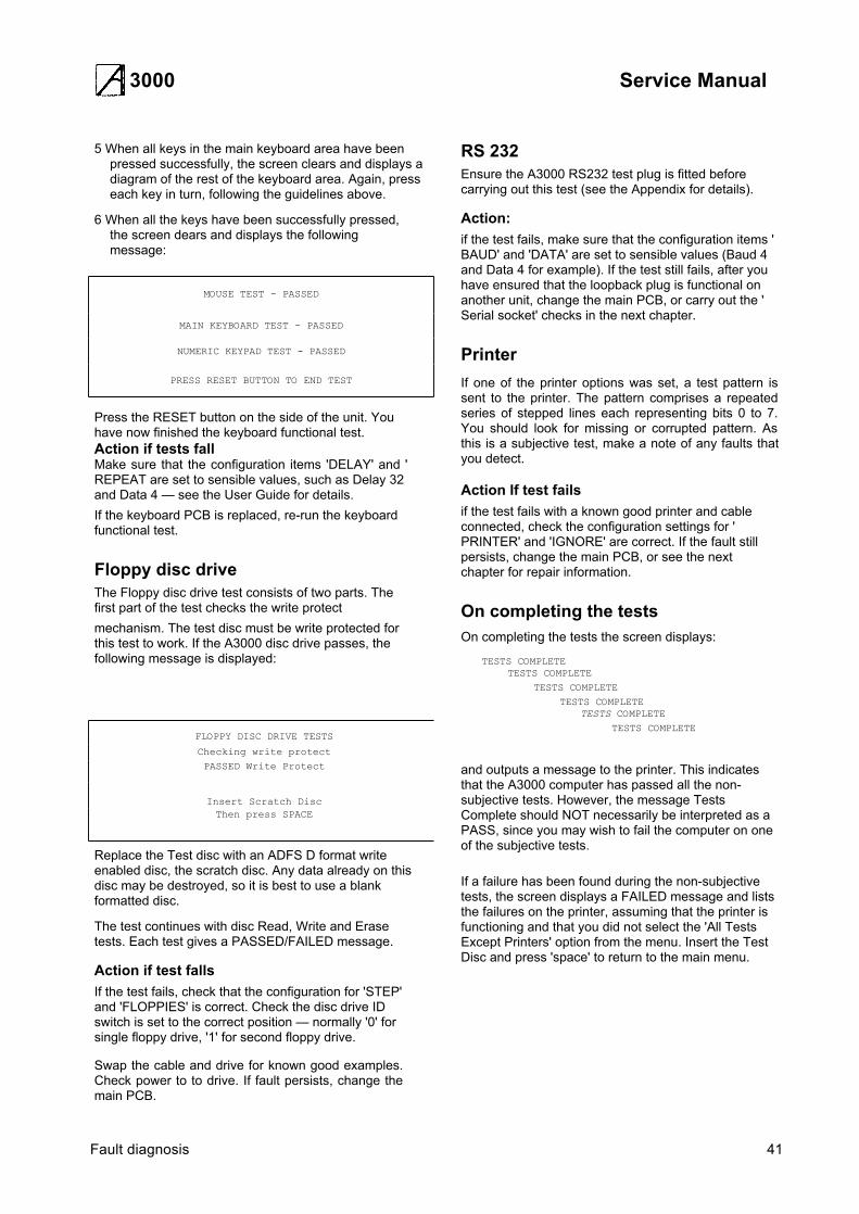
6 When all the keys have been successfully pressed, the screen dears and displays the following message:
MOUSE TEST - PASSED
MAIN KEYBOARD TEST - PASSED
NUMERIC KEYPAD TEST - PASSED
PRESS RESET BUTTON TO END TEST
Press the RESET button on the side of the unit. You have now finished the keyboard functional test. Action if tests fallMake sure that the configuration items 'DELAY' and 'REPEAT are set to sensible values, such as Delay 32 and Data 4 — see the User Guide for details.If the keyboard PCB is replaced, re-run the keyboard functional test.
Floppy disc driveThe Floppy disc drive test consists of two parts. The first part of the test checks the write protectmechanism. The test disc must be write protected for this test to work. If the A3000 disc drive passes, the following message is displayed:
FLOPPY DISC DRIVE TESTS
Checking write protect
PASSED Write Protect
Insert Scratch DiscThen press SPACE
Replace the Test disc with an ADFS D format write enabled disc, the scratch disc. Any data already on this disc may be destroyed, so it is best to use a blank formatted disc.
The test continues with disc Read, Write and Erase tests. Each test gives a PASSED/FAILED message.
Action if test fallsIf the test fails, check that the configuration for 'STEP' and 'FLOPPIES' is correct. Check the disc drive ID switch is set to the correct position — normally '0' for single floppy drive, '1' for second floppy drive.
Swap the cable and drive for known good examples. Check power to to drive. If fault persists, change the main PCB.
RS 232Ensure the A3000 RS232 test plug is fitted before carrying out this test (see the Appendix for details).
Action:if the test fails, make sure that the configuration items 'BAUD' and 'DATA' are set to sensible values (Baud 4 and Data 4 for example). If the test still fails, after you have ensured that the loopback plug is functional on another unit, change the main PCB, or carry out the 'Serial socket' checks in the next chapter.
PrinterIf one of the printer options was set, a test pattern is sent to the printer. The pattern comprises a repeated series of stepped lines each representing bits 0 to 7. You should look for missing or corrupted pattern. As this is a subjective test, make a note of any faults that you detect.
Action If test failsif the test fails with a known good printer and cable connected, check the configuration settings for 'PRINTER' and 'IGNORE' are correct. If the fault still persists, change the main PCB, or see the next chapter for repair information.
On completing the testsOn completing the tests the screen displays:
TESTS COMPLETETESTS COMPLETE
TESTS COMPLETE
TESTS COMPLETETESTS COMPLETE
TESTS COMPLETE
and outputs a message to the printer. This indicates that the A3000 computer has passed all the non-subjective tests. However, the message Tests Complete should NOT necessarily be interpreted as a PASS, since you may wish to fail the computer on one of the subjective tests.
If a failure has been found during the non-subjective tests, the screen displays a FAILED message and lists the failures on the printer, assuming that the printer is functioning and that you did not select the 'All Tests Except Printers' option from the menu. Insert the Test Disc and press 'space' to return to the main menu.
Fault diagnosis 41

3000 Service Manual
Upgrade testsTo test Upgrades fitted to the computer, follow the procedure detailed at the start of the 'Main functional test' section for loading and running the software, then select option 2 from the main Dealer Test Menu. The Upgrades menu will appear:
A3000 Upgrades Test Menu
1 Midi
2 1M Byte Memory3 RS2324 Main Menu
SELECT OPTION:
IntroductionType in the number of the test you wish to run; if it fails, substitute a known good upgrade. If the test still fails, replace the main PCB, or see the next chapter for repair information.
A3000 User Port MIDI Upgrade
IntroductionThe UPM Upgrade functional test should be carried out whenever you install, repair or replace a UPM Upgrade. The suite of programs provide assistance when fault finding, by providing continuous looping.
Note: The MIDI Thru' port is NOT tested.
Equipment requiredIn order to carry out the test, you will require the following equipment:• UPM Upgrade to be tested, which should have
been installed• A3000 Computer• 3.5 inch Test Disc, write protected• Monochrome or analogue RGB monitor.• Acorn Econet cable• User port loopback plug (wired as in the diagram
below)• Dual trace oscilloscope, if you are fault finding.
Connecting the equipmentConnect the:• Computer to the monitor• MIDI IN socket to the MIDI OUT socket, using the
Econet cable• User port loopback plug to the User port• Monitor to the mains supply• A3000 to the mains supply.
Running the testWhen you have selected Midi from the Upgrades menu, the UPM test menu will appear:
A3000 UPM UPGRADE DEALER TESTS
1Functional test.
2Functional test soak.
3Services routines.
Enter choice
Select the appropriate test from the menu; all tests load automatically.
Selections 1 and 2 give a PASSED or FAILED message.
Selections 3 gives a further choice, after which a 'Running message indicates that the selected routine is functioning and the associated signals can be traced with an oscilloscope.
Action if test fallsCheck that the test leads are working and are plugged into the correct sockets. if the test still fails then try using a known working PCB. If this passes then replace the MIDI podule under test, or else replace the main PCB.
1 Mbyte DRAM Expansion TestSelecting 1M Byte Memory from the Upgrades test menu runs the memory upgrade test, which records its progress on the screen:
1 Mbyte Dram Expansion Test
Phase one: incrementing pattern ....
Phase two: TRUE hierarchy ............
Phase three: FALSE hierarchy .........
Phase four: Cycling bits ............
PASSED/FAILED messagePress SPACE to continue.
42 Fault diagnosis

3000 Service Manual
Action if test fallsIf the computer fails the test, restart the system with a delete-power-on and run the test again. If the test still fails, check the connection between the main PCB and the memory expansion card. If test fails yet again, try a known working memory card. If this fails, then replace the main PCB, else replace the faulty memory card.
RS 232 testWhen it has been selected, this test will automatically run and give a PASSED or FAILED message.
Action
If the test fails, make sure that the configuration items 'BAUD' and 'DATA' are set to sensible values (BAUD 4 and DATA 4, for example). If the test still fails, after you have ensured that the loopback plug is functional on another unit, change the main PCB. A diagram for the loopback plug is included in the Appendices.
Fault diagnosis 43

3000 Service Manual
44 Fault diagnosis

3000 Service Manual
Main PCB fault diagnosis & repair
IntroductionThis chapter deals with fault diagnosis and repair of the main PCB at component level.
See the previous chapter for basic fault diagnosis before proceeding to this chapter.
Tools requiredThe suggested tools for fault diagnosis and repair of the A3000 PCB are as follows:• 100 MHz oscilloscope• DC voltmeter• Earth continuity tester (see Appendix B)• Chip extraction tools (68/84 pin)• Soldering/desoldering workstations, capable of
handling both conventional and surface-mounted devices
• Standard handtools.
It is a recommended requirement that anti-static precautions should be utilised at all levels of servicing, ie antistatic matting and wrist-straps.
DANGERAFTER REFITTING OR FITTING AREPLACEMENT ASSEMBLY, CARRY OUTEARTH CONTINUITY TESTING ON THEASSEMBLED COMPUTER ACCORDING TO THEPROCEDURE GIVEN IN APPENDIX B.
WARNINGS• Repairs to multi-layered PCBs:
The main PCB is a four-layer board.Components should only be removed from theboard using equipment specifically designed forthis purpose. For details of suitable equipmentavailable, contact Acorn Customer Service.
• Repairs to surface-mounted devices:The ARM, MEMC, IOC AND VIDC ICs on theA3000 PCB are surface-mounted components.Do not attempt to remove them from the boardand replace them unless you are appropriatelytrained in surface-mount technology and havethe correct equipment to do so. f in doubtcontact Acorn Customer Services.
• System clock failure:f the computer is powered on for more than afew seconds and there is no system clock,there is a risk that all four ARM chips may bedamaged, as well as the RAM.
• Faulty MEMC:f MEMC is faulty or the RAS/CAS signals arenot being generated, the RAM may be damagedif the machine is left on too long. If you suspecta fault in these areas, scope the RAS and CASlines for a few seconds in order to make surethat they still active, then turn the machine off.Do not leave the computer on for more than afew seconds at a time.
• Antistatic precautions:It is a recommended requirement that anti-staticprecautions should be utilised at all levels ofservicing, ie antistatic matting and wrist-straps.
Main PCB fault diagnosis & repair 45
3000 Service Manual
System failureIf the system appears to be dead, proceed as follows:
WARNING: System clock failuref the computer is powered on for more than a fewseconds and there is no system dock, there is arisk that all four ARM chips may be damaged, aswell as the RAM, due to lack of refresh on theDRAM:1 Check RAS and CAS on R133, R129-132.2 Check IC41 pin 19 and IC37 pins 1 and 2 for clock
signals.3 Check for a RAS signal on pin 5 of all the
DRAMS.
1 Check for system RESET — look for a delayed signal on power on (on IC13 pin 29).
2 Check that the signal RST driving IC 44 pin 44 and IC 37 pin 9 is not stuck high.
3 Check for main system clock of 24 MHz on LK28. f absent, check again on IC47, pins 3, 4, 5 and 6, and change IC47 if required. Finally, change the crystal X3.
4 Check SKT 15 for the following: 27C to be CLK 2, 28C to be CLK 8 and 29C to be Ref 8.
5 Check for clocks on IC44 pin 67 and IC41 pin 19.6 Check for the presence and validity of the processor
addresses and PHI 1 clock. This can be done by examining the signals on IC 29 pins 12 to 19, IC 30 pins 12 to 19 and IC 31 pins 12 to 15, whilst holding down the RESET button (RESET can be activated by pressing the RESET key, or by short-circuiting SKT3 pin 15 and 16). When RESET is held down, the address lines will increment (not AO and Al). Should none of the signals toggle, check for the PHI 1 clock on the appropriate IC, at its source on IC 44 pin 66, and on R135. Also check to see that addresses are being presented to the inputs of the above devices. Change ICs 29, 30 or 31 as appropriate, or if no addresses are present, change the ARM — IC 37.
7 Check for all address lines on MEMC, 1C44, again with RESET held down.Check for the presence of LA2 to LA6 and LA16 to LA21 on 1OC IC13.
8 The data bus can be inspected by probing on resistors R49 to R65, R115 to R128 and R87. Note that MEMC1A will not enable the ROMs whilst RESET is activated. By their nature, it is difficult to interpret the signals seen, so just check for the ability of the signals to move between logic states. None of these lines should be stuck permanently high, low or in a midrail state. Any of these resistors may be removed in order to isolate the DRAM bank from the CPU, thus easing the tracing of shorts, etc. Also check for short or open circuits on the BDATA bus, IC 43 pins 12 to 19 and IC 46 pins 12 to 19.
9 Check for shorts on the DRAM address bus, either on the DRAMS themselves or on IC 44 pins 28 to 37. Check all data signals on IC41.
10Check for Data and Address signals on all four of the ROMs. This is especially important if a ROM change has been carried out, as misuse of a screwdriver during ROM removal may havedamaged or broken PCB tracks, socket or ROM legs (an IC extraction tool should have been used).
11 Check the processor interrupt lines FIO and IRO pins 8 and 7 on ARM IC 37. Neither of these should be stuck low. IRO can be expected to pulse low, FIO should be high. These interrupts should also be checked at their source on IOC IC13 pins 50 and 51. Should these also be low, the interrupt source can be traced by examining all interrupt inputs to IOC IC 13 on pins 30 to 42 (note that pins 30, 31 and 42 are active high logic).
46 Main PCB fault diagnosis & repair

3000 Service Manual
Test ROMsThe A3000 Test ROMs are designed to assist in the repair of all A3000 systems where 'Failure to Initialise' faults are present – ie the machine appears to be 'dead' on power-up.
The ROMs contain software which can be categorised in two sections:1 Main memory test routines2 Test routines for use under repetitive reset.To install the test ROMs, carefully remove the RISC OS ROM set, ICs 14, 15, 16 and 17, and replace them with the test ROMs, 1, 2, 3 and 4 respectively:
The test ROMs use the bare minimum of hardware to run the system – remove/disconnect all peripherals not needed for the tests, although a keyboard is needed. A printer can also be connected if required.
Main memory testProviding that the ARM, MEMC and VIDC are functioning, the test ROMs will auto-boot into the menu-driven display below. At any point in the operation of the test ROMs, pressing the RESET key or re-powering the machine will re-start the program and re-display the menu:
0123456789012345678901234567890123456789012345678901234!
Al DIAGNOSTIC TEST ROMS MEMORY SIZE -&0XX00000 BYTES
1. CYCLIC MEMORY TEST WITH PRINTOUT
2. CYCLIC MEMORY TEST
SELECT:
The memory test checks memory according to memory size selected.It is possible that faulty memory may lie in the region
designated as 'screen memory'. f this occurs, the video display may become unreadable. For this reason, the sequence 0123456789 is repeated across the top line of the display. Every 4 digits represent a 32-bit word. Watch for missing or corrupted display.As the start of the screen memory is known to be at physical address &2000000, it should be possible to determine the exact device that is faulty by examining the corruption pattern on the display.The default 'memory size' is &100000 bytes (1 Mbyte), however this may be cycled through 0.5, 1, 2 and 4 Mbyte memory sizes by pressing the 'M' key.When using the ROMs on a machine having memory content other than 1 Mbyte, the video display may at first appear out of line or incorrect. In this instance press the M key repeatedly until the required memory size has been selected.The memory test is cyclic and on completion of each full memory test a full stop (.) will be displayed until it completes one line of the screen. The next completed cycle will move the lefthand full stop down one pixel, and then in sequence across the screen. The 0.5 Mbyte test takes between 3 and 4 seconds to complete whilst the 4 Mbyte test takes about 29 seconds.If for some reason the video display is completely blank or unreadable (eg because of a video fault), a printed output may be obtained by selecting option 1, the output being produced at the printer port as well as on the VDU.
If an error is found in the memory, the display will show:AT ADDRESS &nnnnnnnn WROTE &pppppppp READ xxxxxxxxxxx xxxxxxxxxxxxxxxxxxxxx
(The message will be displayed on one line) where nnnn is the faulty address, pppp is the data written to that address and xxxxxxxx is the data read back from that address in binary form. The least significant bit is the righthand bit.The memory tests do not terminate unless an error is found, in which case after reporting 8 or 9 errors, the test will terminate. Any error will have a cascading effect, so it is good practice to repair the first error displayed first.Note: An additional check is made on the state of CMOS RAM control lines CO and C1 at the beginning of the test, before the display. If either of these lines are short-circuit to 0 Volts, the Test ROMs will indicate this on power-up.
Main PCB fault diagnosis & repair 47

3000 Service Manual
Memory mapPhysical Address IC Numbers
&2000000&2000001&2000002&2000003repeat until&20FFFFF8 2100000to&21FFFFF
IC21 IC20IC22 IC23IC24 IC25IC26 IC27
upgrade
Repetitive reset testThis section of test code is intended for use when the main memory test menu fails to initialise.To make use of this section of the ROMs the following test equipment is required:• Oscilloscope• Signal or pulse generatorThe purpose of the code is to produce certain signals around specific areas of the PCB. These signals may then be monitored using the oscilloscope to assess the operation of that area of the circuit.
A suitable square wave or, preferably, a negative-going pulse generator output at 10 kHz should be connected to the reset line via a component connected to SKT3 pin 13.
After setting the border colour to white, the signals should be observable in the following order, which checks the output selection of IC13 (IOC):
SVPMD lowSVPMD lowSVPMD low
IC44 pin 52and IC37 pin 10
OC CS & S1 hi IC13 pin 67 + pin 63OC CS & S2 hi + pin 62OC CS & S3 hi + pin 61OCCS&S4 hi + pin 59OCCS&S5 hi + pin 58OCCS&S6 hi + pin 57OC CS & S7 hi +pin 56
nB/W lownB/W low IC44 pin 63nB/W low and IC37 pin 84
IOC CS & CO hi IC13 pin 67 + pin 44IOC CS & C1 hi + pin 45IOC CS & C2 hi + pin 4610C CS & C3 hi + pin 47IOC CS & C4h hi + pin 48IOC CS & C5 hi + pin 49IOC CS hi
Repetitive reset test assembler listing
LDRT
LDRT
LDRTLDR
r0,r0,r0,r1,
[r5][1-5][r5]iocmof
;SVPMD pin low ); )continual toggle of:-; )
;re—load ioc base addr. —offset
LDRLDR
1-0,r0,
[r1,r6]![r1, r6]!
;SVPMD pin high;IOC CS pin high ;S1 ioc hi
LDR r0, [r1, r6]! ;IOC CS pin high ;S2 ioc hiLDR r0, [r1, r6]! ;IOC CS pin high ;S3 ioc hiLDR r0, [r1, r6]! ;IOC CS pin high ;S4 ioc hiLDR r0, [r1, r6]! ;IOC CS pin high ;S5 ioc hiLDR r0, [rl, r6]! ;IOC CS pin high ;56 ioc hiLDR r0, [r1, r6]! ;IOC CS pin high ;S7 ioc hi
LDRB r0, [r5] ;nB/W pin high )LDRB r0, [r5] ;nB/W pin high ]
LDRBMOV
r0,r1
[r5]#&FE0000
;nB/W pin high;
)
STR r1, [r7] ; set C0 )
MOV r1 #&FD0000 ; ]
STR r1, [r7] ; set Cl ]
MOV r1 #&FB0000 ; )STR r1, [r7] ; set C2 )MOV r1 #&F70000 ; ) I.O.C.STR r1, [r7] ; set C3 )MOV r1 #&EF0000 ; )STR r1, [r7] ; set C4 )MOV r1 #&DF0000 ; )
STRMOV
rl,r1
[r7]#&FF0000
; set C5;
)
STR r1, [r7] ; reset all
48 Main PCB fault diagnosis & repair
3000 Service Manual
Video faults
Video failure1 Check for +5 V on both ends of L18. If open circuit then
check C100 for a short circuit. Replace L18 and C100 as appropriate. Also check for 3.5 Volts (approx.) on IC 41 pin 43. Should this not be present then check R109, D16 and C93.
2 Check for a 24 MHz clock on IC41 pin 19. f missing then check continuity to and through LK28 and R138.
3 Check for video data on IC41 pins 39, 40 and 41. f not present, check power supply to IC41.
4 Check for short circuits on signals VIDRQ and VIDAK.
5 Check connection of all data lines to VIDC (IC41).6 Finally, change IC41.
Unstable or scrolling displayThe computer may have lost its configuration value for SYNC. Type at the keyboard:*CON. SYNC 1 (RETURN)
Press reset RESET and see if if any change occurs. Investigate configuration failure.
Check for CSYNC signal on SK14 pin 4. If not present, trace back through LK24, R535 and IC40, finally changing VIDC 1041.
Check settings of LK24 and LK27 (see Links table).
Corrupted displayIf the display breaks up around its edges and spurious characters appear then investigate the system oscillator. Suspect IC47or X3.
Check DRAM using the memory test routines.
Colours incorrect or missingWith a full white screen, VIDC IC41 pins 39, 40 and 41 should all have the same signal on them. f not, check pin 43, which should show approximately 3.5V; if not, check R109, C93 and D16. Finally, change VIDC, IC41.
Trace each signal through the periphery circuitry and out to SK14, where the voltage on R, G and B should be the same.
AudioTest the audio with both headphones and internal speakers. Do not forget to issue *SPEAKER ON and *VOLUME 127 commands, if required, making sure that the sound modules are active (see the 'No sound'
algorithm in the previous chapter).If either of the speakers fail, but the headphone socket functions normally, check connections to the main PCB via LK22 and LK23, and check IC32 or 1C38 pin 5 for a signal of 2-3 V amplitude. If no signal is present on pin 5 but can be found on pin 3, change IC32 or 38. Check continuity through R76 and R45 and check that IC13 pin 49 is not stuck high.
If there is no audio at all, first check for +5 V on both ends of L19. f this is open circuit, check the condition of C108 before replacement. Check for about 3 V on VIDC IC41 pin 12. f there is no voltage or a different one, check R500, C107 and C108.
A low amplitude signal should be found on VIDC IC41 pins 13, 14, 15 and 16. f not, change VIDC. These signals can be traced through the peripheral circuitry and out to 011 and 012. The signal amplitude at these points should be about 1.3 V pk-to-pk.
Check for short or open circuit on signals SNDAK and SNDRQ on VIDC IC41 pins 9 and 24.
Configuration, NV memory and RTCIf the NVM suffers data retention problems and the RTC fails, then, with the computer power off, check for about 1.1 V on IC6 pin 8. If this voltage is not present, check R3 and R7. If less then 1V, change the battery B1 and check the operation of D2 and C15.
If the NVM IC6 consistently fails on the same data bits, change the device.If the clock fails to run or runs inaccurately, checkand if necessary replace X2. LK7 allows access to the clock signal.
Main PCB fault diagnosis & repair 49

3000 Service Manual
Peripheral faults
Keyboard and mouseMake sure that the configuration items DELAY and REPEAT are set to sensible values - see the A3000 User Guide.
Check computer interface by swapping to a known good keyboard or mouse.
Floppy disc driveMake sure that the configuration items STEP and FLOPPIES are correctly set. Check that the disc drive ID selection switch is in the zero position. Swap the disc drive for a known good drive and cable. f this also fails, check the power supply connection for +5 V and 0 V.
If the computer is not recognising the drive, check that all cables are connected both to the drive and to the PCB, and that power is present on the power cable. Also check that the drive ID plate has not fallen off inside the drive and jammed it.
PrinterMake sure that the configuration items for IGNORE and PRINT are set to sensible values. Swap the printer for a known good printer and cable.
If the printer fails completely, check for a STROBE signal on Q1 collector; trace back through R36 and IC18. Also check for shorts or open circuits on PACK and PBSY on pins 2 and 4 of 1C9, and 11 and 13 of IC8.
If the data printed is incorrect, check the continuity of the data lines into and out of IC 11, though the series resistors and onto SK 10.
If both the printer and the floppy disc drive fail, change IC 18.Capacitors C23 to C33 on the printer portoccasionally go open circuit. These should be checked if printer problems are being experienced.
Serial port (upgrade)Check that the upgrade has been correctly installed. Make sure that the configuration items BAUD and DATA are set to sensible values. Check for =+10V on IC7 pin 1 and =-10V on pin 24. Check for the clock on IC 1 pins 6 and 7; change X1 if faulty. f OK, change IC1 and IC7.
Expansion cardsRun the relevant expansion card test; if it fails, substitute a known good expansion card. f the test still fails, check through System failure, tracing all signals through to the expansion card socket SK15 (external) or SK3 and 11 (internal). f necessary, replace expansion card backplane.
WARNINGPower down the computer before fitting or removingan external expansion card.
50 Main PCB fault diagnosis & repair

3000 Service Manual
Parts lists
The parts lists in this chapter detail the components used in the manufacture of the computer and its upgrades. Contact the Spares Department of Acorn Computers Limited (account holders only), or its authorised dealers and Approved Service Centres, for information as to which parts are available as spares.
Final assembly parts list
Part no. Description Qty
1 0060,000/A FINAL ASSEMBLY DRAWING 1*3 0176.005 DISC DRIVE CABLE ASSY 14 0276,038 'NO ECONET' LABEL 15 0276,106 RESET BUTTON 17 0180,000 AVON MAIN PCB ASSY 18 0180.010 22W 240V PSU 19 0160,011 KEYBOARD (UK) 110 0180,012 MAINS CABLE ASSY 111 0180,081 SPEAKER ASSEMBLY 212 0183,004 3.5x1" 1MB DISC DRIVE 114 0260,061 LOWER MOULDING 115 0260.062 UPPER MOULDING 116 0260,063 BATTERY COVER 117 0280.073 BLANKING PANEL 118 0260,074 LOCK PLATE 219 0260,075 CABLE RESTRAINT PLATE 120 0260,077 PSU COVER 121 0280,078 PSU INSULATION SHEET 123 0480,041 BBC/LED LABEL 124 0480,042 BASE LABEL 125 0480.043 'NO SERIAL' LABEL 126 0480,044 REAR MAINS LABEL 127 0480,047 ACORN LOGO LABEL 129 0860,024 GMAT CBL RND 7,4Dx4T BLK 130 0940,007 ADH HOT-MELT A/R31 0882,770 SCW No2x1/4" PLST PAN POS 132 0882.716 SCW No4x1/4" PLST PAN POS 233 0662,111 SCW M2.5x6 PAN HD POSI 434 0662,121 SCW M3x6 PAN HD POSI 435 0862,711 SCW No4x3/4" PLST PAN POS 136 0682,730 SCW No6x3/8" PLST PAN POS 137 0882,971 WSHR M2,5 SPRF IT STL 238 0884,048 RIVET PLST DOME 3,1Dx4THK 139 0691,026 LABEL HiVOLT40mmSq MAX SA 140 0890,013 FOOT S/A RUBR 8Dx2.5Hmm 2
'per batch
PCB assembly parts listItem Part no. Description Qty
1 0260,000 BARE PCB 12 0160.000/A AVON PCB ASSEMBLY DWG 1*3 0180,000/C AVON PCB CIRCUIT DIAGRAM 1*6 0280,072 PCB BACK PANEL 19 0800,070 CONR 2W SHUNT 0.1" 10
(FITTED TO LK17-20,24-29)10 0800,126 SKT IC 24/0.3" NORM (IC7) 111 0800,128 SKT IC 28/0.6" NORM (IC1) 112 0600,132 SKT IC 32/0.6" SUPA (IC14-17) 413 0800,140 SKT IC 40/0.6" NORM 11C215 0870,422 WIRE 25SWG CPR TIN A/R
(X1,X2,X3)17 0902,004 LABEL SERIAL PCB 15x50mm 119 xxxx,xxx RIVET AVDEL 11070312 (SKIS) 2
R1 0521,102 RES 1K0 SW 5% 0W25 1206 1R2 0521.102 RES 1 K0 SMD 5% 0W25 1206 1R3 0521,181 RES 160R SMD 5%0W25 1206 1R4 0521,331 RES 330R SMD 5% 0W25 1206 1R5 0521,271 RES 270R SMD 5% 0W25 1206 1R6 N/FR7 0521,181 RES 160R SMD 5%0W25 1206 1R6 0521.101 RES 100R SMD 5% 0W25 1206 1R9 0521223 RES 22K SMD 5% 0W25 1206 1R10 0521,472 RES 4K7 SMD 5% 0W25 1206 1R11 0521,102 RES 1 K0 SMD 5% 0W25 1206 1R12 0521,472 RES 4K7 SMD 5% 0W25 1206 1R13 0521,472 RES 4K7 SW 5%0W25 1206 1R14 0521,331 RES 330R SMD 5% 0W25 1206 1R15 0521,222 RES 2K2 SMD 5% 0W25 1206 1R16-R24 0521,220 RES 22R SW 5% 0W25 1206 9R25-R28 0521,472 RES 4K7 SW 5%0W25 1206 4R29 0521,102 RES 1K0 SW 5% 0W25 1206 1R30 0521,472 RES 4K7 SMD 5% 0W25 1206 1R31 0521,472 RES 4K7 SMD 5% 0W25 1206 1R32 0521,103 RES 10K SMD 5% 0W25 1206 1R33 0521,103 RES 10K SMD 5% 0W25 1206 1R34 0521,331 RES 330R SW) 5% 0W25 1206 1R35 0521,331 RES 330R SW) 5% 0W25 1206 1R36 0521,102 RES 1K0 SW 5% 0W25 1206 1R37 0521,104 RES 100K SMD 5% 0W25 1206 1R36 0521,104 RES 100K SMD 5% 0W25 1206 1R39 0521,104 RES 100K SMD 5% 0W25 1206 1R40 0521,103 RES 10K SMD 5% 0W25 1206 1R41 0521,104 RES 100K SMD 5% 0W25 1206 1R42 0521,104 RES 100K SMD 5% 0W25 1206 1R43 0521,102 RES 1K0 SMD 5% 0W25 1206 1R44 0521,472 RES 4K7 SMD 5% 0W25 1206 1R45 0521,562 RES 5K6 SMD 5% 0W25 1206 1R46 0521,681 RES 680R SW 5%0W25 1206 1R47 0521,100 RES 10R SW 5% 0W25 1206 1R48 0521,122 RES 1K2 SMD 5% 0W25 1206 1R49-R65 0521,680 RES 66R SMD 5% 0W25 1206 17R66 0521,331 RES 330R SMD 5% 0W25 1206 1R67-R71 0521,220 RES 22R SMD 5% 0W25 1206 5R72-R75 0521,472 RES 4K7 SMD 5% 0W25 1206 4R76 0521,562 RES 5K6 SW 5% 0W25 1206 1R77 0521,681 RES 660R SMD 5% 0W25 1206 1R76 0521,100 RES 10R SMD 5% 0W25 1206 1R79 0506,250 RES 332R MF 1%0W25 E96 1R80 0521,330 RES 33R SMD 5% 0W25 1206 1R61 0521,332 RES 3K3 SMD 5%0W25 1206 1R82 0507,223 RES 22K MF 1% 0W25 1R83 0506250 RES 332R ME 1% 0W25 E96 1R84 0521.560 RES 56R SMD 5% 0W25 1206 1R85 0521,332 RES 3K3 SMD 5% 0W25 1206 1R86 0507,223 RES 22K MF 1% 0W25 1R87 0521,680 RES 68R SMD 5% 0W25 1206 1
Main PCB fault diagnosis & repair 51

3000 Service Manual
Item Part no. Description Qty
R88 0521,332 RES 3K3 SMD 5% 0W25 1206 1R89 0521,332 RES 3K3 SMD 5% 0W25 1206 1R90 0521,560 RES 56R SMD 5% 0W25 1206 1R91 0507,223 RES 22K MF 1% 0W25 1R92 0521,332 RES 3K3 SMD 5% 0W25 1206 1R93 0507,223 RES 22K MF 1% 0W25 1R94 0521,560 RES 56R SMD 5% 0W25 1206 1R95 0507,223 RES 22K MF 1% 0W25 1R96 0506,250 RES 332R MF 1% 0W25 E96 1R97 0507,223 RES 22K MF 1% 0W25 1R96 0507,223 RES 22K MF 1% 0W25 1R99 0507,223 RES 22K MF 1% 0W25 1R100 0521,330 RES 33R SMD 5% 0W25 1206 1R101 0521,332 RES 3K3 SMD 5% 0W25 1206 1R102 0506,161 RES 43R2 MF 1% 0W25 E96 1R103 0506,161 RES 43R2 MF 1% 0W25 E96 1R104 0506,161 RES 43R2 MF 1% 0W25 E96 1R105 0521,681 RES 680R SW 5%0W25 1206 1R106 0521,103 RES 10K SMD 5%0W25 1206 1R107 0521,103 RES 10K SMD 5% 0W25 1206 1R108 0521,331 RES 330R SMD 5% 0W25 1206 1R109 0521,103 RES 10K SMD 5% 0W25 1206 1R110-R115 0506,300 RES 1K00 MF 1% 0W25 E96 4R114 0521,122 RES 1K2 SMD 5% 0W25 1206 1R115-R128 0521,680 RES 68R SMD 5% 0W25 1206 14R129-R133 0521,220 RES 22R SMD 5% 0W25 1206 5R134 0521,122 RES 1K2 SMD 5% 0W25 1206 1R135 0521,330 RES 33R SMD 5% 0W25 1206 1R136 0521,221 RES 220R SMD 5% 0W25 1206 1R137 0521,103 RES 10K SMD 5% 0W25 1206 1R138 0521,680 RES 68R SMD 5% 0W25 1206 1R139 0521,680 RES 68R SMD 5% 0W25 1206 1R140 0521,680 RES 68R SMD 5% 0W25 1206 1R141 0521,220 RES 22R SMD 5% 0W25 1206 1R142 0521,220 RES 22R SMD 5% 0W25 1206 1R143 0521,220 RES 22R SMD 5% 0W25 1206 1R144 0521,103 RES 10K SMD 5% 0W25 1206 1R145 0521,472 RES 4K7 SMD 5% 0W25 1206 1R500 0521,333 RES 33K SWD 5% 0W25 1206 1R501 0521,103 RES 10K SMD 5% 0W25 1206 1R502 0521,472 RES 4K7 SMD 5% 0W25 1206 1R503-R518 0521,680 RES 68R SMD 5% 0W25 1206 16R519-R529 0521,104 RES 100K SMD 5%0W25 1206 11R530 0521,102 RES 1K0 SMD 5% 0W25 1206 1P531 0521,181 RES 180R SMD 5%0W25 1206 1R532 0521,820 RES 82R SMD 5% 0W25 1206 1R533 0521,331 RES 330R SMD 5% 0W25 1206 1R534 0521,680 RES 68R SMD 5% 0W25 1206 1R535 0521,680 RES 68R SMD 5% 0W25 1206 1R536 0521221 RES 220R WO 5% 0W25 1206 1R537 0521,680 RES 68R SMD 5% 0W25 1206 1R538 0521,221 RES 220R SMD 5% 0W25 1206 1R539 0521,680 RES 68R SMD 5% 0W25 1206 1R540 0521,221 RES 220R SMD 5% 0W25 1206 1R541 0521,680 RES 68R SW) 5% 0W25 1206 1P542 0521,221 RES 220R SMD 5% 0W25 1206 1R543-R546 0521,102 RES 1 K0 SMD 5% 0W25 1206 4R547 0521,472 RES 4K7 SMD 5% 0W25 1206 1R548 0521,472 RES 4K7 SMD 5% 0W25 1206 1R549 0521,104 RES 100K SMD 5% 0W25 1206 1R550 0521,472 RES 4K7 SMD 5% 0W25 1206 1R551 0521,472 RES 4K7 SMD 5% 0W25 1206 1R552 0521,472 RES 4K7 SMD 5% 0W25 1206 1R553 0521221 RES 220R SMD 5% 0W25 1206 1P554 0521,103 RES 10K SMD 5% 0W25 1206 1R555 N/FR556 N/FP557 0521,473 RES 47K SMD 5% 0W25 1206 1R558 N/FR559 N/FR560 0521,331 RES 330R SMD 5% 0W25 1206 1R561 0521,271 RES 270R SW 5% 0W25 1206 1
Item Part no. Description Qty
R562 N/FR563 N/FR564 0521,473 RES 47K SW 5% 0W25 1206R565 0521,473 RES 47K SMD 5% 0W25 1206 1R566R567- N/FR571 0521,473 RES 47K SMD 5% 0W25 1206 5R572 0521,221 RES 220R SMD 5% 0W25 1206 1R573-R579 N/F
CI 0681,001 PCPCTR DCPLR 33n SMD 1210 1C2 0631.033 CPCTR CPLT 33p 30V 2% 1C3 0640,473 CPCTR CER 47n 30V 80% 1C4 0610,010 CPCTR TANT 10u 10V 20% 1C5 0681,001 CPCTR DCPLR 33n SMD 1210 1C6-C10 0635,100 CPCTR ALEC 10u 16V RAD 5C11 0681,001 CPCTR DCPLR 33n SMD 1210 1C12 0635230 CPCTR ALEC 220u 16V RAD 1C13 0610,010 CPCTR TANT 10u 10V 20% 1C14 0635,230 CPCTR ALEC 220u 16V RAD 1C15 0635,470 CPCTR ALEC 47u 16V RAD 1C16 0631,012 CPCTR CPLT 12p 30V 2% 1C17 0681,001 CPCTR DCPLR 33n SMD 1210 1C18 0681,001 CPCTR DCPLR 33n SMD 1210 1C19 0635,100 CPCTR ALEC 10u 16V RAD 1C20 0681,001 CPCTR DCPLR 33n SMD 1210 1C21 0681,001 CPCTR DCPLR 33n SMD 1210 1C22 0610,010 CPCTR TANT 10u 10V 20% 1C23 0631,100 CPCTR CPLT 100p 30V 2% 1C24-C31 0630,220 CPCTR CPLT 2n2 30V 10% 8C32 0631,100 CPCTR CPLT 100p 30V 2% 1C33 0631,100 CPCTR CPLT 100p 30V 2% 1C34 0610,010 CPCTR TANT 10u 10V 20% 1C35 0681,001 CPCTR DCPLR 33n SMD 1210 1C36 0681,001 CPCTR DCPLR 33n SMD 1210 1C37 0681,001 CPCTR DCPLR 33n SMD 1210 1C38 N/FC39 0621,470 CPCTR ALEC 47u 10V AX 1C40-C47 0681,001 CPCTR DCPLR 33n SMD 1210 8C48 0681,003 CPCTR DCPLR 100n SMD 1210 1C49 0681,003 CPCTR DCPLR 100n SMD 1210 1C50-054 0681,001 CPCTR DCPLR 33n SMD 1210 5C55 0610,010 CPCTR TANT 10u 10V 20% 1C56 0681,003 CPCTR DCPLR 100n SMD 1210 1C57 0610,010 CPCTR TANT 10u 10V 20% 1C58 0681,003 CPCTR DCPLR 100n SMD 1210 1C59 0681,001 CPCTR DCPLR 33n SMD 1210 1C60 0635,470 CPCTR ALEC 47u 16V RAD 1C61 0635,230 CPCTR ALEC 220u 16V RAD 1C62 0640,473 CPCTR CER 47n 30V 80% 1C63 0635,470 CPCTR ALEC 47u 16V RAD 1C64 0681,001 CPCTR DCPLR 33n SMD 1210 1C65 0642,103 CPCTR ALEC 100u 25V RAD 1C66 0635,230 CPCTR ALEC 220u 16V RAD 1C67 0635,047 CPCTR ALEC 4u7 16V RAD 1C68 0640,473 CPCTR CER 47n 30V 80% 1C69 0635,230 CPCTR ALEC 220u 16V RAD 1C70 0642,103 CPCTR ALEC 100u 25V RAD 1C71 0681,003 CPCTR DCPLR 100n SMD 1210 1C72 0681,003 CPCTR DCPLR 100n SMD 1210 1C73 0681,003 CPCTR DCPLR 100n SMD 1210 1C74 0640,473 CPCTR CER 47n 30V 80% 1C75 0630,220 CPCTR CPLT 2n2 30V 10% 1C76 0681,001 CPCTR DCPLR 33n SMD 1210 1C77 0650223 CPCTR MPSTR 22n 50V 10% 1C78 0610,010 CPCTR TANT 10u 10V 20% 1C79 0630,100 CPCTR CPLT 1n 30V 10% 1C80 0650,106 CPCTR MPSTR 100n 50V 10% 1C81 0630,220 CPCTR CPLT 2n2 30V 10% 1C82 0630,220 CPCTR CPLT 2n2 30V 10% 1C83 0621,470 CPCTR ALEC 47u 10V AX 1C84 0681,003 CPCTR DCPLR 100n SMD 1210 1
52 Main PCB fault diagnosis & repair

3000 Service Manual
Item Part no. Description Qty
C85 0630,100 CPCTR CPLT 1n 30V 10% 1C86 0630,220 CPCTR CPLT 2n2 30V 10% 1C87 0681,001 CPCTR DCPLR 33n SW) 1210 1C88 0650,106 CPCTR MPSTR 100n 50V 10% 1C89 0610,010 CPCTR TANT 10u 10V 20% 1C90 0630,220 CPCTR CPLT 2n2 30V 10% 1C91 0630,220 CPCTR CPLT 2n2 30V 10% 1C92 0650,223 CPCTR MPSTR 22n 50V 10% 1C93 0635,100 CPCTR ALEC 10u 16V RAD 1C94 0610,010 CPCTR TANT 10u 10V 20% 1C95 0635,470 CPCTR ALEC 47u 16V RAD 1C96 0640,473 CPCTR CER 47n 30V 80% 1C97 0635,100 CPCTR ALEC 10u 16V RAD 1C98 0681,001 CPCTR DCPLR 33n SW) 1210 1C99 0681,001 CPCTR DCPLR 33n SW) 1210 1C100 0610,010 CPCTR TANT 10u 10V 20% 1C101 N/FC102 N/FC103 N/FC104 N/FC105 0681,001 CPCTR DCPLR 33n SMD 1210 1C106 0681,001 CPCTR DCPLR 33n SW) 1210 1C107 0640,473 CPCTR CER 47n 30V 80% 1C108 0610,010 CPCTR TANT 10u 10V 20% 1C109 0621,470 CPCTR ALEC 47u 10V AX 1C110 0621,470 CPCTR ALEC 47u 10V AX 1C111 0610,010 CPCTR TANT l0u 10V 20% 1C112 0635,230 CPCTR ALEC 220u 16V RAD 1C113 0681,001 CPCTR DCPLR 33n SMD 1210 1C114 0631,010 CPCTR CPLT 10p 30V 2% 1C115 0631,033 CPCTR CPLT 33p 30V 2% 1C116 0630,270 CPCTR CPLT 2n7 30V 10% 1C500-0506 0681,001 CPCTR DCPLR 33n SMD 1210 7
IC1 N/FIC2 0280,022 IC KBD CNTRLR (0708,051) 1IC3 0740,038 IC 7438 TTL 14/0.3" 1IC4 0742,145 IC 74LS145 TTL 16/0.3 1ICS 0742,145 IC 74LS145 TTL 16/0.3 1IC6 0708,583 IC 8583 RTC RAM 8/0.3" 1IC7 N/FIC8 0749,014 IC 74HCT14 CMOS 14/0.3" 1IC9 0747,004 IC 74HC04 CMOS 14/0.3" 1IC10 0747,074 IC 74HC74 CMOS 14/0.3" 1IC11 0742,374 IC 74LS374 TTL 20/0.3' 1IC12 0747,138 IC 74HC138 CMOS 16/0.3" 1IC13 2201,368 IC 10C (PLSTC) 1IC14 0283.022 RISC OS ROM 1 V2.0 1IC15 0283,023 RISC OS ROM 2 V2.0 1IC16 0283,024 RISC OS ROM 3 V2.0 1IC17 0283,025 RISC OS ROM 4 V2.0 1IC18 0747,574 IC 74HC574 CMOS 20.0.3" 1IC19 0747,574 IC 74HC574 CMOS 20.0.3" 1IC20-IC27 0704,118 IC DRAM 256Kx4 120n 20ZIP 8IC28 0747,139 IC 741HC139 CMOS 16/0.3" 1IC29 0747,573 IC 74HC573 CMOS 20/0.3" 1IC30 0747,573 IC 74HC573 CMOS 20/0.3" 1IC31 0747,573 IC 74HC573 CMOS 20/0.3" 11C32 0770,386 IC LM386 AUDIO AMP 1IC33 0747,139 IC 74HC139 CMOS 16/0.3" 1IC34 0747,000 IC 74HC00 CMOS 14/0.3" 1IC35 0740,006 IC 7406 TTL 14/0.3" 1
0740,016 IC 7416 TTL 14/0.3" (OPTION)IC36 0701,772 IC 1772 FDC 28/0.6' 1IC37 2201,365 IC ARM Rum PLSTC) 1IC38 0770,386 IC LM386 AUDIO AMP 1IC39 0770,324 IC LM324 QUAD OP AMP 11C40 0750,086 IC 74AC86 CMOS 14/0.3" 1IC41 2201,367 IC VIDC 1A (PLSTC) 1IC42 0749,573 IC 74HCT573 CMOS 20/0.3" 1IC43 0747,573 IC 74HC573 CMOS 20/0.3" 1IC44 2201,375 IC MEMC 1 A {PLSTC-8MHz) 1IC45 0749,573 IC 74HCT573 CMOS 20/0.3' 1IC46 0747,573 IC 74HC573 CMOS 20/0.3" 1IC47 0747,004 IC 74HC04 CMOS 14/0.3" 1
Item Part no. Description Qty
01 0780,241 TRANS 8C239 NPN 0.2"P LDS 102-010 0783,907 TRANS 2N3906 PNP .2"P LDS 9011 0780,241 TRANS BC239 NPN 0.2"P LDS 1012 0780,241 TRANS BC239 NPN 0.2-P LDS 1D1 N/F02 0794,005 DIODE SI 1N4005 600V 1A 1D3-D16 0794,148 DIODE SI 1N4148 14
B10817,013
BAT NICAD 1V2 280mAH PCB 1
L1- (0500,000 RES ZERO-OHM 0W25 (0.6"ptch) 14L14 (0870,420 WIRE 22SWG TIN (OPTION)L15 N/FL16 0860,015 CHOKE RF FE BEAD 1L17 0860,015 CHOKE RF FE BEAD 1L18 0860,012 CHOKE RF 2u2H AX 0-30 1L19 0860,005 COIL RF 33uH AX 0-45 1L20 0860,015 CHOKE RF FE BEAD 1L21 0860,015 CHOKE RF FE BEAD 1
LK 1-LK16 N/FLK17 0800,050 CONR 2W WAFR 0.1" ST PCB 1LK18 0800,050 CONR 2W WAFR 0.1" ST PCB 111(19 0800,051 CONR 3W WAFR 0.1" ST PCB 1LK20 0800,051 CONR 3W WAFR 0.1' ST PCB 1LK21 N/FLK22 0800,458 CONR 2W WAFR 0.1" ST LK 2LK23 0800,458 CONR 2W WAFR 0.1" ST LK 2LK24 0800,051 CONR 3W WAFR 0.1" ST PCB 1LK25 0800,050 CONR 2W WAFR 0.1" ST PCB 11K26 0800.050 CONR 2W WAFR 0.1" ST PCB 1LK27 0800,050 CONR 2W WAFR 0.1" ST PCB 1LK28 0800,050 CONR 2W WAFR 0.1" ST PCB 1LK29 0800,050 CONR 2W WAFR 0.1" ST PCB 1LK30 0800,050 CONR 2W WAFR 0.1" ST PCB 1LK31 0800,050 CONR 2W WAFR 0.1" ST PCB 1
PL 1 0180,013 EARTH STRAP {PCB/PSU} 1PL2 0800,291 CONRD 9W PLG RAPCB+RFI+LK 1PL3 0800.203 FSTN TAB 6,3mmx0,8 ST PCB 1PL4 0800,203 FSTN TAB 6,3mmx0,8 ST PCB 1PL5 N/FPL6 0803,102 CONR 34W BOX IDC LP ST 1
SKI 0800,920 CONR 9W MINDIN RA PCB 1SK2 0800,004 CONR SW SKT DIN RA PCB 1SK3 0800,487 CONR 17W SKT 0.1" PCB 1SK4 0800,487 CONR 17W SKI' 0.1" PCB 1SK5 0800,481 CONR 5W SKT HSNG 0.1" PCB 1SK6 0801,202 CONR 20W 0.1" FLXPCB SKT 1SK7 0801,202 CONR 20W 0.1" FLXPCB SKT 1SK8 0800,486 CONR 5W SKT 0.1" PCB 1SK9 0800.486 CONR 5W SKT 0.1" PCB 1SK10 0800,293 CONRD 25W SKT RAPCB+RFI+L 1SK11 0800,487 CONR 17W SKT 0.1" PCB 1SK12 0800,642 CONR JKSKT 3W 3,5mm RAPCB 1SK13 0800,611 CONR PHONO SKT RA PCB 1SK14 0800,292 CONRD 9W SKT RAPCB+RFI+LK 1SKIS 0800,411 CONR 64W SKT RA AC PCB 1SK16 0800,476 CONR 20W WAFR 0.1 ST 10mm 3
SW1 0805,704 SW 2P MOM CO P/B RA PCB 1
X1 0820,019 XTAL 1.8432MHz HC18 1X2 0821,327 XTAL 32.768KHz CC 0.05' 1X3 0820240 XTAL 24.00MHz HC18 1
Main PCB fault diagnosis & repair 53

3000 Service Manual
2Mb RAM upgrade
Item Part no. Description thy
1 0280,200 BARE PCB 12 0180,200/A ASSEMBLY DRAWING 1*3 0180,200/C CIRCUIT DIAGRAM 1*
C 1-C8 0680,102 CPCTR DCPLR 100n AXA 25V 8C9 0635,470 CPCTR 47u ALEC 16V RAD 1C10 0635,470 CPCTR 47u ALEC 16V RAD 1
IC1-1C8 0704,118 IC DRAM 256Kx4 120n 20ZIP 8
SK1 0800,488 CONR 20W SKT 0 . r RA PCB 1SK2 0800,488 CONR 20W SKT 0.1" RA PCB 1SK3 0800,488 CONR 20W SKT 0.1" RA PCB 1
•per batch
User Port MIDI upgrade
Item Part no. Description Qty
2 0180,300/A ASSEMBLY DRAWING 1 "3 0180,300/C CIRCUIT DIAGRAM 1*6 0280,360 PCB REAR PANEL 19 0800,128 SKT IC 28/0.6" NORM 11C311 0884,042 RIVET POP DOME 3,2D & THK 2
(USE ON ITEM 6)
L1 -L18 0500,000 RES ZERO R 0W25 18
R1 0502.222 RES 21(2 C/MF 5% 0W25 1R2 0502222 RES 21(2 C/MF 5% 0W25 1R3 0502,221 RES 220R C/MF 5% 0W25 1R4 0502,221 RES 220R C/MF 5% 0W25 1R5 0502,221 RES 220R C/MF 5% 0W25 1R6 0502,221 RES 220R C/MF 5% 0W25 1R7 0502,102 RES 1K0 C/MF 5% 0W25 1R8 0502,222 RES 2K2 C/MF 5% 0W25 1R9 0502,222 RES 2K2 C/MF 5% 0W25 1RI0 0502,221 RES 220R C/MF 5% 0W25 1R11 0502,103 RES 10K C/MF 5%0W25 1R12 0502,103 RES 10K C/MF 5%0W25 1
C1 0635,230 CPCTR 220u ALEC 16V RAD 1C2-C8 0680,002 CPCTR DCPLR 33/47n 0.2" 7
IC 1 0706,525 IC 65C22 VIA CMOS 2MHz 1IC2 0799,504 OPTO ISOL 6N138 8/0.3" 1IC3 0280,320 ROM (0727,128/9 TBP) 1IC4 0740,006 IC 7406 TTL 14/0.3" 1ICS 0732,691 IC 2691 UART CMOS 24/0.3" 1IC6 0747,139 IC 74HC139 CMOS 16/0.3" 1
D1 0794,148 DIODE 1N4148 SI 1
LK 1-LK4 N/F
SK1 0800,009 CONR 20W HDR IDC RA 4WALL 1SK2 0800,004 CONR SW SKT DIN RA PCB 1SK3 0800,004 CONR 5W SKT DIN RA PCB 1SK4 0800,004 CONR 5W SKT DIN RA PCB 1SK5 0800,475 CONR 17W WAFR 0.1 23,5mmL 1SK6 0800,475 CONR 17W WAFR 0.1 23,5mmL 1
• per batch
54 Main PCB fault diagnosis & repair

3000 Service Manual
Appendix A: Serial port loopback plug
Serial port loopback plug
Parts list*
Item Part no. Description Qty
1 0276.081 CIRCUIT 8 ASSEMBLY DRAWING 1'3 0800,288 CONR 9W SCKT 'D' ST MS SB 15 0800,991 CONR 9W SHELL D' + SCREWS 1
R1 0502,122 RES 1K2 C/MF 5% 0W25 1R2 0502,122 RES 1K2 C/MF 5% 0W25 1R3 0502,122 RES 1K2 C/MF 5%0W25 1R4 0502,122 RES 1K2 C/MF 5% 0W25 1R5 0502,472 RES 4K7 C/MF 5% 0W25 1R6 N/FR7 0502,472 RES 4K7 C/MF 5% 0W25 1R8 0502,472 RES 4K7 C/MF 5% 0W25 1
D1 0790,085 DIODE BAT85 SBL 1D1 0790,085 DIODE BAT85 SBL 1
per batch
Assembly notes
Assemble the components onto 'Veroboard', and fit item 5 (the shell) to protect the assembly
Main PCB fault diagnosis & repair 55

3000 Service Manual
56 Main PCB fault diagnosis & repair
3000 Service Manual
Appendix B: Earth continuity testing
Equipment requiredAn earth continuity tester capable of sourcing 25A derived from an AC source with a no-load voltage not exceeding 12V.
It is recommended that the calibration and operation of the instrument be checked frequently enough to assure its accuracy.
Test Procedure
DANGERTHE FOLLOWING TESTS INVOLVE HIGHCURRENTS BUT LOW VOLTAGES. ALLNECESSARY PRECAUTIONS MUST BE TAKENTO ENSURE OPERATOR SAFETY DURINGTESTING.
DANGERSWITCH OFF THE COMPUTER, DISCONNECT ITFROM THE MAINS SUPPLY, AND DISCONNECTANY PERIPHERALS BEFORE CARRYING OUTTHIS TEST.
The test should be performed on a fully assembled computer.
Using the Earth continuity tester, check the continuity between the power supply cord 13A plug earth pin and the following points:-
1 the rear panel internal expansion card fixing screws2 both printer/parallel port D-type fixing bolts.The resistance measured between the earth pin and
each of the above test points shall not exceed 0.15 a This value includes an allowance for the resistance of the mains cable. The duration of each test shall not exceed 10 seconds. No waiting period between tests is necessary.
Main PCB fault diagnosis & repair 57