Embed Size (px)
Citation preview

DR0
GD0
OutP
REFRTN
VIN
DR1
DR5
Primary power supply
Voltage feedback pin
Voltage output
High Power LED Arrays
Q1
RDHC
GND
GND
RISNS1
RISNS2
RISNS6
GND GND
Q2
Q6
GD1
SE0
Faultb
D1
VRAIL
U1
LM3463
SE1
SE5
GD5
REFRTN
RIADJ2
RIADJ1
CVCC
Vcc
VREF
IOUTADJ
GND
CFLTCDHC
FCAP
CDHC
RFS
FS
VCC
MODE
DIM01
DIM23
DIM4
DIM5
EN
RFB1
RFB2
CIN
VLedFB
REFRTN
GND
GND
Faultb
MODE
DIM01
DIM23
DIM4
DIM5
EN
CVREF
RLMT1DRVLIM
RLMT2
LM3463
www.ti.com SNVS807A –MAY 2012–REVISED MAY 2013
Dynamic Headroom Controller with Thermal Control Interface and Individual ChannelDimming Control
Check for Samples: LM3463
1FEATURES APPLICATIONS2• Dynamic Headroom Control Output to • Streetlights
Maximize Efficiency • Solid State Lighting Solutions• 6 Channels Current Regulated LED Driver
DESCRIPTION• High Precision Analog Dimming ControlThe LM3463 is a six channel linear LED driver withInterfaceDynamic Headroom Control (DHC) interface that is• 4 Individual PWM Dimming Control Inputspecialized for high power LED lighting applications.
• Dimming Control via Digital Data Bus The variation of the output current of every outputchannel in the temperature range of -40°C to 125°C• Built-In Maximum MOSFET Power Limitingis well controlled to less than ±1%. The output currentMechanismof every channel is accurately matched to each other• Allows Cascade Operation to Extend thewith less than ± 1% difference as well.Output ChannelsBy interfacing the LM3463 to the output voltage• Fault Indicator Outputfeedback node of a switching power supply via the
• Thermal Shutdown DHC interface, the system efficiency is optimized• UVLO With Hysteresis automatically. The dynamic headroom control circuit
in the LM3463 minimizes power dissipation on the• 48L WQFN Packageexternal MOSFETs by adjusting the output voltage ofthe primary switching power supply according to theKEY SPECIFICATIONSchanging forward voltage of the LEDs. Comprising
• Wide supply voltage range (12V-95V) the advantages of linear and switching converters,the LM3463 delivers accurately regulated current to• Thermal fold-back dimming controlLEDs while maximizing the system efficiency.• DHC regulates the lowest MOSFET drainThe dimming control interface of the LM3463 acceptsvoltage to 1Vboth analog and PWM dimming control signals. Theanalog dimming control input controls the current ofall LEDs while the PWM control inputs control thedimming duty of output channels individually.
Typical Application
1
Please be aware that an important notice concerning availability, standard warranty, and use in critical applications ofTexas Instruments semiconductor products and disclaimers thereto appears at the end of this data sheet.
2All trademarks are the property of their respective owners.
PRODUCTION DATA information is current as of publication date. Copyright © 2012–2013, Texas Instruments IncorporatedProducts conform to specifications per the terms of the TexasInstruments standard warranty. Production processing does notnecessarily include testing of all parameters.
DR0
DR1
DR2
DR3
DR4
DR5V
IN
IOUTADJ
VREF
EN
GN
D
REFRTN
FS
Faultb
SYNC
MO
DE
DIM01
DIM23
DIM4
DIM5
CD
HC
DR
VLI
M
CLKOUT
FC
AP
Out
P
VLe
dFB
ISR
VC
C
GD
0
SE
0
GD
1
SE
1
GD
2
SE
2
GD
3
SE
3
GD
4
SE
4
GD
5
SE
5
NC
NC
NC
NC
NC
NC
NC
NC
1
2
3
4
5
6
7
8
9
10
11
12
242322212019181716151413
25
26
27
28
29
30
31
32
33
34
35
36
48 47 46 45 44 43 42 41 40 39 38 37
EP
LM3463
SNVS807A –MAY 2012–REVISED MAY 2013 www.ti.com
DESCRIPTION CONTINUEDThe LM3463 provides a sophisticated protection mechanism that secures high reliability and stability of thelighting system. The protection features include VIN Under-Voltage–Lock-Out (UVLO), thermal shut-down, LEDshort / open circuit protection and MOSFET drain voltage limiting. The LED short circuit protection protects boththe LED and MOSFETS by limiting the power dissipation on the MOSFETS.
Connection Diagram
Figure 1. TOP VIEW48-Lead Plastic WQFNPackage Number RHS
PIN DESCRIPTIONSPin Name Description Application information
0V reference for small signal return This pin should connect to the end points of current sensing resistors with1 REFRTN paths individual connections to ensure channel to channel current accuracy.
The current of all output channels (defined by RISNSn) reduces according2 IOUTADJ Output current level adjust pin to the voltage at this pin. This pin should connect to the VREF pin when
output current reduction is not required.
This pin is the output of a precision reference voltage regulator. This pin3 VREF Precision reference voltage output must be bypassed through a ceramic capacitor to REFRTN.
Device enable pin with internal pull-up
4 EN Enable input Enable: VEN = Floating
Disable: VEN = GND
Frequency setting pin. Connect a resistor across this pin to GND to set theinternal oscillator frequency.Internal oscillator control or external5 FS clock input pin The internal clock frequency can be defined by forcing an external clocksignal to this pin.
Fault indicator output. This pin is an open-drain output and is pulled low6 Faultb Fault indicator output when an open circuit of LED string is identified.
2 Submit Documentation Feedback Copyright © 2012–2013, Texas Instruments Incorporated
Product Folder Links: LM3463

LM3463
www.ti.com SNVS807A –MAY 2012–REVISED MAY 2013
PIN DESCRIPTIONS (continued)
Pin Name Description Application information
The function of this pin differs depending on the selected operation modeMulti-function input pin. that sets by the MODE pin.
Direct PWM mode: Apply a bi-level PWM signal (TTL logic high and low)Channel 0/1 PWM dimming control to this pin to enable/disable ch0 and ch1. Apply logic high to this pin to
7 DIM01 enable channel 0 and 1.
Serial data input In serial interface mode, this pin is configured as the serial data input.
In DC interface mode, the voltage on this pin is converted into PWMDC voltage dimming control dimming duty for channel 0 and 1.
The function of this pin differs depending on the selected operation modeMulti-function input pin. that sets by the MODE pin.
Direct PWM mode: apply bi-level PWM signal (TTL logic high and low) toChannel 2/3 PWM dimming control this pin to enable/disable ch2 and ch3. Apply a logic high to this pin to
enable both channel 2 and 3.8 DIM23In serial interface mode, this pin is configured as the serial clock signalSerial clock input input.
In DC interface mode, the voltage on this pin is converted into PWMDC voltage dimming control dimming duty for channel 2 and 3.
The function of this pin differs depending on the selected operation modeMulti-function input pin. that sets by the MODE pin.
Direct PWM mode: apply bi-level PWM signal to this pin to enable/disableChannel 4 dimming control channel 4. Apply logic high to this pin to enable channel 4.
In serial interface mode, this pin is configured as load pulse input, pulling9 DIM4 this pin low will latch the shifted-in data into internal register of the
Load data control pin LM3463. This pin is pulled low if the requested load operation is notcompleted. User should check the status of this pin before writing data intothe LM3463 through this pin.
In DC interface mode, the voltage on this pin is converted into PWMDC voltage dimming control dimming duty for channel 4.
The function of this pin differs depending on the selected operation modeMulti-function input pin. that sets by the MODE pin.
Direct PWM mode: Apply a bi-level PWM signal (TTL logic high and low)Channel 5 dimming control to this pin to enable/disable channel 5. Apply a logic high to this pin to
10 DIM5 enable channel 5.
Serial operation mode This pin should connect to GND when serial operation mode is selected.
In DC interface mode, the voltage on this pin is converted into PWMDC voltage dimming control dimming duty for channel 5.
Serial control signal output pin for cascade operation. This signalSerial data output for cascade synchronizes with the rising edge of the CLKOUT signal and carriesoperation information to the slave devices to turn on LEDs.11 SYNCSync. pulse input in direct PWM This is a synchronization signal input pin for the slave device to performmode LED pretest upon system startup.
Dimming clock output for cascade Dimming clock output for cascade operation. The frequency at this pin12 CLKOUT operation / Sync pulse output for equal to 1/2 of the internal clock or externally applied clock frequency.
Direct PWM mode
Connect a resistor from this pin to GND to set the additional bias current13 ISR Start up current control pin to the CDHC upon system startup.
The voltage on this pin defines the threshold of the drain voltage of theexternal MOSFETs (VDRn) to begin output current reduction.
As the VDRn exceeds VDRVLIM, the LED driving current reduces according14 DRVLIM MOSFET power limit setting inputto the increasing of VDRn at certain fixed rate. This function prevents theMOSFET from over-heating. The maximum power dissipation is limited toVDRVLIM * ILED(per ch.).
Dynamic headroom control time Connect a capacitor (CDHC) from this pin to ground to program the DHC15 CDHC constant capacitor loop response.
Connect a capacitor, CFLT from this pin to ground to program the fault de-16 FCAP Fault de-bounce capacitor bounce time.
17 GND System ground This pin should connect to the system ground
Copyright © 2012–2013, Texas Instruments Incorporated Submit Documentation Feedback 3
Product Folder Links: LM3463
LM3463
SNVS807A –MAY 2012–REVISED MAY 2013 www.ti.com
PIN DESCRIPTIONS (continued)
Pin Name Description Application information
Operation mode selection input pin. Bias this pin externally to set theLM3463 in different operation mode.
Direct PWM mode: VMODE = GND18 MODE Mode select input pinSerial interface mode: VMODE = No Connection
DC interface mode: VMODE = VCC
Output terminal of the internal voltage regulator. This pin should be19 VCC Internal regulator output bypassed to GND through a 1uf ceramic capacitor.
This pin detects the output voltage of the primary power supply (VRAIL).LEDs will be turned on when the voltage at this pin reaches 2.5V.20 VLedFB Rail voltage detection input pinConnect this pin to VCC to set a device as a slave.
This pin is an open drain output (current sink) which should connect to the21 OutP DHC output Driver output voltage feedback node of the primary power supply through a
resistor and a diode to realize rail voltage adjustment.
22 NC No connection
Supply voltage input pin. This pin should be bypassed to GND using a 1uF23 VIN System supply ceramic capacitor.
24 NC No connection
Connect to the junction of the drain terminal of the external MOSFET andChannel 5 drain voltage feedback25 DR5 the cathode of the LED string. This pin is connected to the internalinput to facilitate DHC comparator to facilitate DHC.
26 NC No connection
Connect to the junction of the drain terminal of the external MOSFET andChannel 4 drain voltage feedback27 DR4 the cathode of the LED string. This pin is connected to the internalinput to facilitate DHC comparator to facilitate DHC.
28 NC No connection
Connect to the junction of the drain terminal of the external MOSFET andChannel 3 drain voltage feedback29 DR3 the cathode of the LED string. This pin is connected to the internalinput to facilitate DHC comparator to facilitate DHC.
30 NC No connection
Connect to the junction of the drain terminal of the external MOSFET andChannel 2 drain voltage feedback31 DR2 the cathode of the LED string. This pin is connected to the internalinput to facilitate DHC comparator to facilitate DHC.
32 NC No connection
Connect to the junction of the drain terminal of the external MOSFET andChannel 1 drain voltage feedback33 DR1 the cathode of the LED string. This pin is connected to the internalinput to facilitate DHC comparator to facilitate DHC.
34 NC No connection
Connect to the junction of the drain terminal of the external MOSFET andChannel 0 drain voltage feedback35 DR0 the cathode of the LED string. Voltage on this pin is being fed to theinput to facilitate DHC internal comparator to facilitate DHC.
36 NC No connection
Channel 5 LED driver sense input Connect to the junction of the source terminal of the external MOSFET37 SE5 pin and the sense resistor to facilitate current regulation for channel 5.
38 GD5 channel 5 gate drive output pin Gate driver output. Connect to the gate terminal of the external MOSFET.
Channel 4 LED driver sense input Connect to the junction of the source terminal of the external MOSFET39 SE4 pin and the sense resistor to facilitate current regulation for channel 4.
40 GD4 channel 4 gate drive output pin Gate driver output. Connect to the gate terminal of the external MOSFET.
Channel 3 LED driver sense input Connect to the junction of the source terminal of the external MOSFET41 SE3 pin and the sense resistor to facilitate current regulation for channel 3.
42 GD3 channel 3 gate drive output pin Gate driver output. Connect to the gate terminal of the external MOSFET.
Channel 2 LED driver sense input Connect to the junction of the source terminal of the external MOSFET43 SE2 pin and the sense resistor to facilitate current regulation for channel 2.
44 GD2 channel 2 gate drive output pin Gate driver output. Connect to the gate terminal of the external MOSFET.
Channel 1 LED driver sense input Connect to the junction of the source terminal of the external MOSFET45 SE1 pin and the sense resistor to facilitate current regulation for channel 1.
4 Submit Documentation Feedback Copyright © 2012–2013, Texas Instruments Incorporated
Product Folder Links: LM3463

LM3463
www.ti.com SNVS807A –MAY 2012–REVISED MAY 2013
PIN DESCRIPTIONS (continued)
Pin Name Description Application information
46 GD1 channel 1 gate drive output pin Gate driver output. Connect to the gate terminal of the external MOSFET.
Channel 0 LED driver sense input Connect to the junction of the source terminal of the external MOSFET47 SE0 pin and the sense resistor to facilitate current regulation for channel 0.
48 GD0 channel 0 gate drive output pin Gate driver output. Connect to the gate terminal of the external MOSFET.
Connect to the GND pin. The EP has no internal connection to ground andEP Thermal Pad must connect to the GND pin externally. Place 9 vias from EP to copper
ground plane.
Copyright © 2012–2013, Texas Instruments Incorporated Submit Documentation Feedback 5
Product Folder Links: LM3463
LM3463
SNVS807A –MAY 2012–REVISED MAY 2013 www.ti.com
These devices have limited built-in ESD protection. The leads should be shorted together or the device placed in conductive foamduring storage or handling to prevent electrostatic damage to the MOS gates.
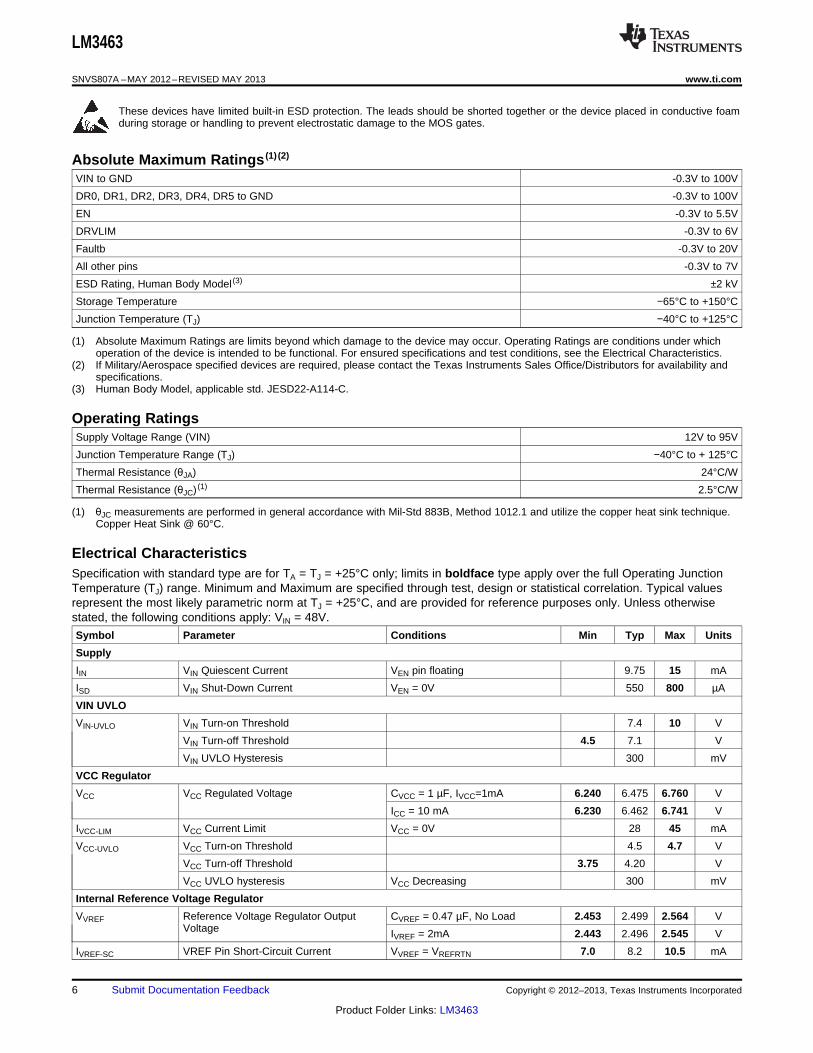
Absolute Maximum Ratings (1) (2)
VIN to GND -0.3V to 100V
DR0, DR1, DR2, DR3, DR4, DR5 to GND -0.3V to 100V
EN -0.3V to 5.5V
DRVLIM -0.3V to 6V
Faultb -0.3V to 20V
All other pins -0.3V to 7V
ESD Rating, Human Body Model (3) ±2 kV
Storage Temperature −65°C to +150°C
Junction Temperature (TJ) −40°C to +125°C
(1) Absolute Maximum Ratings are limits beyond which damage to the device may occur. Operating Ratings are conditions under whichoperation of the device is intended to be functional. For ensured specifications and test conditions, see the Electrical Characteristics.
(2) If Military/Aerospace specified devices are required, please contact the Texas Instruments Sales Office/Distributors for availability andspecifications.
(3) Human Body Model, applicable std. JESD22-A114-C.
Operating RatingsSupply Voltage Range (VIN) 12V to 95V
Junction Temperature Range (TJ) −40°C to + 125°C
Thermal Resistance (θJA) 24°C/W
Thermal Resistance (θJC) (1) 2.5°C/W
(1) θJC measurements are performed in general accordance with Mil-Std 883B, Method 1012.1 and utilize the copper heat sink technique.Copper Heat Sink @ 60°C.
Electrical CharacteristicsSpecification with standard type are for TA = TJ = +25°C only; limits in boldface type apply over the full Operating JunctionTemperature (TJ) range. Minimum and Maximum are specified through test, design or statistical correlation. Typical valuesrepresent the most likely parametric norm at TJ = +25°C, and are provided for reference purposes only. Unless otherwisestated, the following conditions apply: VIN = 48V.
Symbol Parameter Conditions Min Typ Max Units
Supply
IIN VIN Quiescent Current VEN pin floating 9.75 15 mA
ISD VIN Shut-Down Current VEN = 0V 550 800 µA
VIN UVLO
VIN-UVLO VIN Turn-on Threshold 7.4 10 V
VIN Turn-off Threshold 4.5 7.1 V
VIN UVLO Hysteresis 300 mV
VCC Regulator
VCC VCC Regulated Voltage CVCC = 1 µF, IVCC=1mA 6.240 6.475 6.760 V
ICC = 10 mA 6.230 6.462 6.741 V
IVCC-LIM VCC Current Limit VCC = 0V 28 45 mA
VCC-UVLO VCC Turn-on Threshold 4.5 4.7 V
VCC Turn-off Threshold 3.75 4.20 V
VCC UVLO hysteresis VCC Decreasing 300 mV
Internal Reference Voltage Regulator
VVREF Reference Voltage Regulator Output CVREF = 0.47 µF, No Load 2.453 2.499 2.564 VVoltage IVREF = 2mA 2.443 2.496 2.545 V
IVREF-SC VREF Pin Short-Circuit Current VVREF = VREFRTN 7.0 8.2 10.5 mA
6 Submit Documentation Feedback Copyright © 2012–2013, Texas Instruments Incorporated
Product Folder Links: LM3463
LM3463
www.ti.com SNVS807A –MAY 2012–REVISED MAY 2013
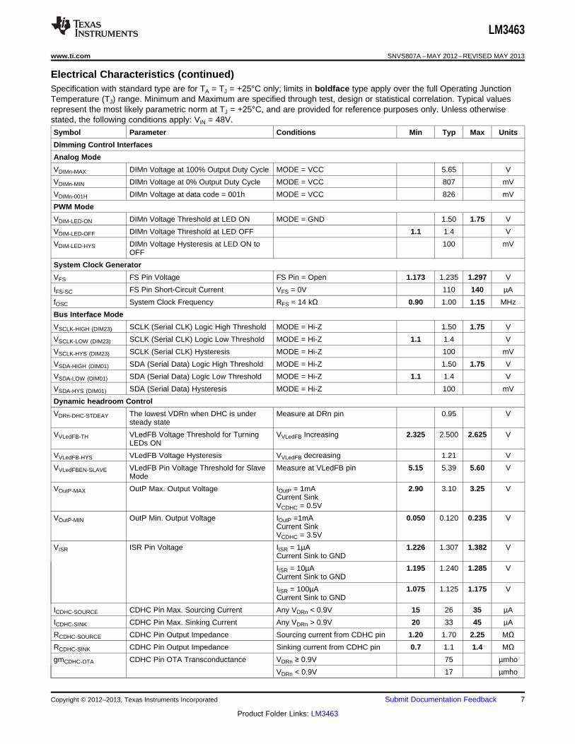
Electrical Characteristics (continued)Specification with standard type are for TA = TJ = +25°C only; limits in boldface type apply over the full Operating JunctionTemperature (TJ) range. Minimum and Maximum are specified through test, design or statistical correlation. Typical valuesrepresent the most likely parametric norm at TJ = +25°C, and are provided for reference purposes only. Unless otherwisestated, the following conditions apply: VIN = 48V.
Symbol Parameter Conditions Min Typ Max Units
Dimming Control Interfaces
Analog Mode
VDIMn-MAX DIMn Voltage at 100% Output Duty Cycle MODE = VCC 5.65 V
VDIMn-MIN DIMn Voltage at 0% Output Duty Cycle MODE = VCC 807 mV
VDIMn-001H DIMn Voltage at data code = 001h MODE = VCC 826 mV
PWM Mode
VDIM-LED-ON DIMn Voltage Threshold at LED ON MODE = GND 1.50 1.75 V
VDIM-LED-OFF DIMn Voltage Threshold at LED OFF 1.1 1.4 V
VDIM-LED-HYS DIMn Voltage Hysteresis at LED ON to 100 mVOFF
System Clock Generator
VFS FS Pin Voltage FS Pin = Open 1.173 1.235 1.297 V
IFS-SC FS Pin Short-Circuit Current VFS = 0V 110 140 µA
fOSC System Clock Frequency RFS = 14 kΩ 0.90 1.00 1.15 MHz
Bus Interface Mode
VSCLK-HIGH (DIM23) SCLK (Serial CLK) Logic High Threshold MODE = Hi-Z 1.50 1.75 V
VSCLK-LOW (DIM23) SCLK (Serial CLK) Logic Low Threshold MODE = Hi-Z 1.1 1.4 V
VSCLK-HYS (DIM23) SCLK (Serial CLK) Hysteresis MODE = Hi-Z 100 mV
VSDA-HIGH (DIM01) SDA (Serial Data) Logic High Threshold MODE = Hi-Z 1.50 1.75 V
VSDA-LOW (DIM01) SDA (Serial Data) Logic Low Threshold MODE = Hi-Z 1.1 1.4 V
VSDA-HYS (DIM01) SDA (Serial Data) Hysteresis MODE = Hi-Z 100 mV
Dynamic headroom Control
VDRn-DHC-STDEAY The lowest VDRn when DHC is under Measure at DRn pin 0.95 Vsteady state
VVLedFB-TH VLedFB Voltage Threshold for Turning VVLedFB Increasing 2.325 2.500 2.625 VLEDs ON
VVLedFB-HYS VLedFB Voltage Hysteresis VVLedFB decreasing 1.21 V
VVLedFBEN-SLAVE VLedFB Pin Voltage Threshold for Slave Measure at VLedFB pin 5.15 5.39 5.60 VMode
VOutP-MAX OutP Max. Output Voltage IOutP = 1mA 2.90 3.10 3.25 VCurrent SinkVCDHC = 0.5V
VOutP-MIN OutP Min. Output Voltage IOutP =1mA 0.050 0.120 0.235 VCurrent SinkVCDHC = 3.5V
VISR ISR Pin Voltage IISR = 1µA 1.226 1.307 1.382 VCurrent Sink to GND
IISR = 10µA 1.195 1.240 1.285 VCurrent Sink to GND
IISR = 100µA 1.075 1.125 1.175 VCurrent Sink to GND
ICDHC-SOURCE CDHC Pin Max. Sourcing Current Any VDRn < 0.9V 15 26 35 µA
ICDHC-SINK CDHC Pin Max. Sinking Current Any VDRn > 0.9V 20 33 45 µA
RCDHC-SOURCE CDHC Pin Output Impedance Sourcing current from CDHC pin 1.20 1.70 2.25 MΩRCDHC-SINK CDHC Pin Output Impedance Sinking current from CDHC pin 0.7 1.1 1.4 MΩgmCDHC-OTA CDHC Pin OTA Transconductance VDRn ≥ 0.9V 75 µmho
VDRn < 0.9V 17 µmho
Copyright © 2012–2013, Texas Instruments Incorporated Submit Documentation Feedback 7
Product Folder Links: LM3463
LM3463
SNVS807A –MAY 2012–REVISED MAY 2013 www.ti.com
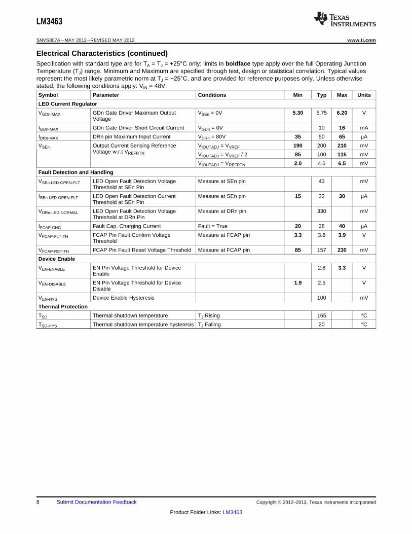
Electrical Characteristics (continued)Specification with standard type are for TA = TJ = +25°C only; limits in boldface type apply over the full Operating JunctionTemperature (TJ) range. Minimum and Maximum are specified through test, design or statistical correlation. Typical valuesrepresent the most likely parametric norm at TJ = +25°C, and are provided for reference purposes only. Unless otherwisestated, the following conditions apply: VIN = 48V.
Symbol Parameter Conditions Min Typ Max Units
LED Current Regulator
VGDn-MAX GDn Gate Driver Maximum Output VSEn = 0V 5.30 5.75 6.20 VVoltage
IGDn-MAX GDn Gate Driver Short Circuit Current VGDn = 0V 10 16 mA
IDRn-MAX DRn pin Maximum Input Current VDRn = 80V 35 50 65 µA
VSEn Output Current Sensing Reference VIOUTADJ = VVREF 190 200 210 mVVoltage w.r.t VREFRTN VIOUTADJ = VVREF / 2 85 100 115 mV
VIOUTADJ = VREFRTN 2.0 4.6 6.5 mV
Fault Detection and Handling
VSEn-LED-OPEN-FLT LED Open Fault Detection Voltage Measure at SEn pin 43 mVThreshold at SEn Pin
ISEn-LED-OPEN-FLT LED Open Fault Detection Current Measure at SEn pin 15 22 30 µAThreshold at SEn Pin
VDRn-LED-NORMAL LED Open Fault Detection Voltage Measure at DRn pin 330 mVThreshold at DRn Pin
IFCAP-CHG Fault Cap. Charging Current Fault = True 20 28 40 µA
VFCAP-FLT-TH FCAP Pin Fault Confirm Voltage Measure at FCAP pin 3.3 3.6 3.9 VThreshold
VFCAP-RST-TH FCAP Pin Fault Reset Voltage Threshold Measure at FCAP pin 85 157 230 mV
Device Enable
VEN-ENABLE EN Pin Voltage Threshold for Device 2.6 3.3 VEnable
VEN-DISABLE EN Pin Voltage Threshold for Device 1.9 2.5 VDisable
VEN-HYS Device Enable Hysteresis 100 mV
Thermal Protection
TSD Thermal shutdown temperature TJ Rising 165 °C
TSD-HYS Thermal shutdown temperature hysteresis TJ Falling 20 °C
8 Submit Documentation Feedback Copyright © 2012–2013, Texas Instruments Incorporated
Product Folder Links: LM3463
-40 -20 0 20 40 60 80 100 120 140
0.10
0.12
0.15
0.16
0.18
0.20
0.22
0.24
0.26
0.29
VS
EnC
H-C
H V
aria
tion
(%)
TA(°C)
VIOUTADJ=VREF
-40 -20 0 20 40 60 80 100 120 140
0.20
0.25
0.30
0.35
0.40
0.45
0.50
0.56
VS
EnC
H-C
H V
aria
tion
(%)
TA(°C)
VIOUTADJ=0.5*VREF
-40 -20 0 20 40 60 80 100 120 140
-0.8
-0.6
-0.4
-0.2
0.0
0.2
0.4
0.6
0.8
ûV
SE
n(%
)
TA(°C)
VIOUTADJ=VREF
CH0CH1CH2CH3CH4CH5
-40 -20 0 20 40 60 80 100 120 140
-1.5
-1.0
-0.5
0.0
0.5
1.0
1.5
ûV
SE
n(%
)
TA(°C)
VIOUTADJ=0.5*VREF
CH0CH1CH2CH3CH4CH5
-40 -20 0 20 40 60 80 100 120 140
0.198
0.199
0.200
0.201
0.202
0.203
VS
En(
V)
TA(°C)
VIOUTADJ= VREF
CH0CH1CH2CH3CH4CH5
-40 -20 0 20 40 60 80 100 120 140
99.0
99.5
100.0
100.5
101.0
101.5
102.0
102.5
103.0
VS
En(
mV
)
TA(°C)
VIOUTADJ=0.5*VREF
CH0CH2CH3CH4CH5
LM3463
www.ti.com SNVS807A –MAY 2012–REVISED MAY 2013
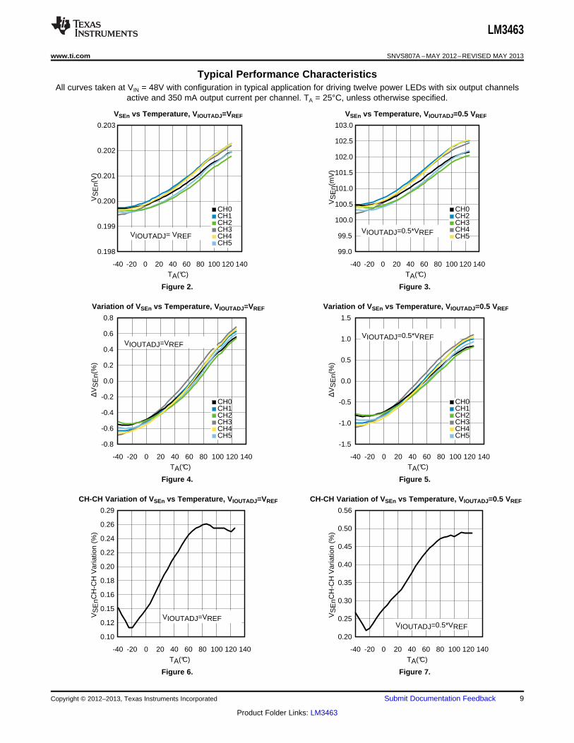
Typical Performance CharacteristicsAll curves taken at VIN = 48V with configuration in typical application for driving twelve power LEDs with six output channels
active and 350 mA output current per channel. TA = 25°C, unless otherwise specified.
VSEn vs Temperature, VIOUTADJ=VREF VSEn vs Temperature, VIOUTADJ=0.5 VREF
Figure 2. Figure 3.
Variation of VSEn vs Temperature, VIOUTADJ=VREF Variation of VSEn vs Temperature, VIOUTADJ=0.5 VREF
Figure 4. Figure 5.
CH-CH Variation of VSEn vs Temperature, VIOUTADJ=VREF CH-CH Variation of VSEn vs Temperature, VIOUTADJ=0.5 VREF
Figure 6. Figure 7.
Copyright © 2012–2013, Texas Instruments Incorporated Submit Documentation Feedback 9
Product Folder Links: LM3463
0.0 0.5 1.0 1.5 2.0 2.5
0.000
0.025
0.050
0.075
0.100
0.125
0.150
0.175
0.200
VS
En(
V)
VIOUTADJ(V)
TA=-40°C
0 10 20 30 40 50 60
0
2
4
6
8
10
12
VS
En(
mV
)
VIOUTADJ(mV)
TA=-40°C
CH0CH1CH2CH3CH4CH5
0.0 0.5 1.0 1.5 2.0 2.5
0.000
0.025
0.050
0.075
0.100
0.125
0.150
0.175
0.200
VS
En(
V)
VIOUTADJ(V)
TA=25°C
0 10 20 30 40 50 60
0
2
4
6
8
10
12
VS
En(
mV
)
VIOUTADJ(mV)
TA=25°C
CH0CH1CH2CH3CH4CH5
0.0 0.5 1.0 1.5 2.0 2.5
0.000
0.025
0.050
0.075
0.100
0.125
0.150
0.175
0.200
VS
En(
V)
VIOUTADJ(V)
TA=125°C
0 10 20 30 40 50 60
0
2
4
6
8
10
12
VS
En(
mV
)
VIOUTADJ(mV)
TA=125°C
CH0CH1CH2CH3CH4CH5
LM3463
SNVS807A –MAY 2012–REVISED MAY 2013 www.ti.com
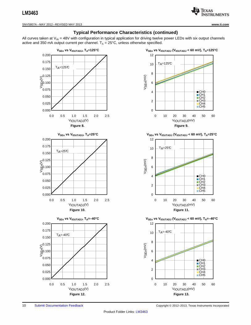
Typical Performance Characteristics (continued)All curves taken at VIN = 48V with configuration in typical application for driving twelve power LEDs with six output channelsactive and 350 mA output current per channel. TA = 25°C, unless otherwise specified.
VSEn vs VIOUTADJ, TA=125°C VSEn vs VIOUTADJ (VIOUTADJ < 60 mV), TA=125°C
Figure 8. Figure 9.
VSEn vs VIOUTADJ, TA=25°C VSEn vs VIOUTADJ (VIOUTADJ < 60 mV), TA=25°C
Figure 10. Figure 11.
VSEn vs VIOUTADJ, TA=–40°C VSEn vs VIOUTADJ (VIOUTADJ < 60 mV), TA=–40°C
Figure 12. Figure 13.
10 Submit Documentation Feedback Copyright © 2012–2013, Texas Instruments Incorporated
Product Folder Links: LM3463
-40 -20 0 20 40 60 80 100 120 140
6.40
6.42
6.44
6.46
6.48
6.50
6.52
6.54
6.56
VC
C(V
)
TA(°C)-40 -20 0 20 40 60 80 100 120 140
8.50
8.56
8.60
8.65
8.70
8.75
8.80
8.85
8.90
8.95
9.00
OP
ER
AT
ING
I IN
(mA
)
TA(°C)
-40 -20 0 20 40 60 80 100 120 140
3.00
3.05
3.10
3.15
3.20
3.25
3.30
3.35
3.40
3.45
3.50
VO
utP
-MA
X(V
)
TA(°C)-40 -20 0 20 40 60 80 100 120 140
2.46
2.46
2.48
2.48
2.50
2.50
2.51
2.52
2.53
2.54
2.55
VR
EF
(V)
TA(°C)
LM3463
www.ti.com SNVS807A –MAY 2012–REVISED MAY 2013
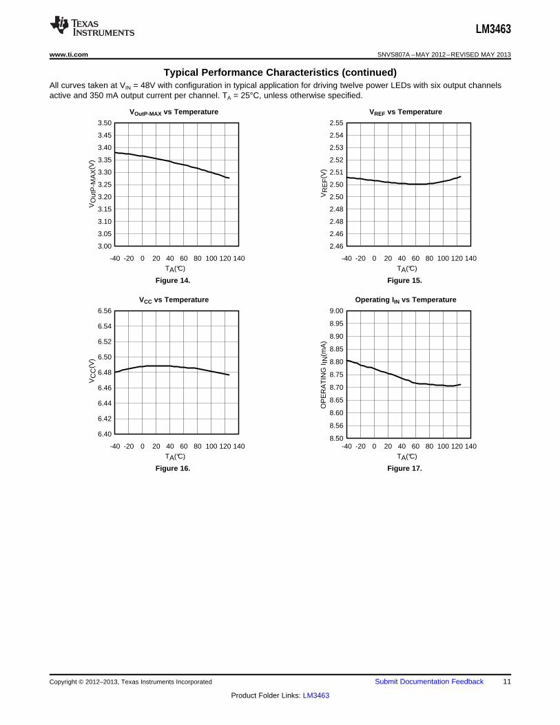
Typical Performance Characteristics (continued)All curves taken at VIN = 48V with configuration in typical application for driving twelve power LEDs with six output channelsactive and 350 mA output current per channel. TA = 25°C, unless otherwise specified.
VOutP-MAX vs Temperature VREF vs Temperature
Figure 14. Figure 15.
VCC vs Temperature Operating IIN vs Temperature
Figure 16. Figure 17.
Copyright © 2012–2013, Texas Instruments Incorporated Submit Documentation Feedback 11
Product Folder Links: LM3463
GD0
SE0Ref1
S/H
Fault
DR2
GD1
SE1Ref1
S/H
Fault
GD2
SE2Ref1
S/H
Fault
GD3
SE3Ref1
S/H
Fault
GD4
SE4Ref1
S/H
Fault
GD5
SE5Ref1
S/H
Fault
Fault/Control Logic
High voltage Fault detection circuitry
DR3
DR4
DR5
DR0
DR1
DHC circuitryCDHC
OutP
Faultb
FCAP
Pre-Regulator VIN
VCC
EN
GND
Output currentcontrol circuitry
IOUTADJ
ISR
Ref1 VBG
ADCRef
VLedFB
MODE
DIM01
DIM23
DIM4
DIM5
Mode Control
Inpu
t Int
erfa
ce
Serial IF
32 b
it sh
ift r
egis
ter
PC
LK
C25
5Lo
ad
SYNC
Mod
e C
ontr
olC
223
Shi
ft E
nabl
e
Pul
se W
idth
Con
trol
ler
C25
5
PC
LK
Ser
ial I
F
LM3463VREF
REFRTN
DRVLIM
SAR ADC
Oscillator (ADC, duty cycle control)
FS
5 to 1 MUX
CLK
OU
T
8-bit Timing Decoder
PCLK
C22
3
C25
5
LM3463
SNVS807A –MAY 2012–REVISED MAY 2013 www.ti.com
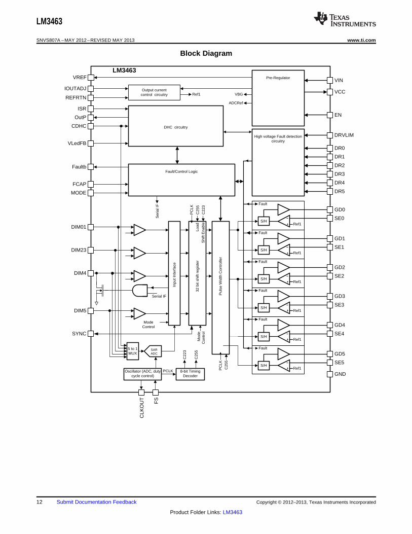
Block Diagram
12 Submit Documentation Feedback Copyright © 2012–2013, Texas Instruments Incorporated
Product Folder Links: LM3463

DHC CircuitVREF
Regulator
VCCLM3463
DRn
GDn
SEn
GND
IOUTADJ
VREF
REFRTN
RIADJ1
RIADJ2RISNSn
To LEDCathode
LM3463
www.ti.com SNVS807A –MAY 2012–REVISED MAY 2013
Overview
The LM3463 is a six channel linear current regulator which designed for LED lighting applications. The use of theDynamic Headroom Control (DHC) method secures high system power efficiency and prolongs system operationlifetime by minimizing the power stress on critical components. The output currents of the LM3463 driver stageare regulated by six individual low-side current regulators.
The current regulators are accompanied by a high precision current sensing circuit. In order to ensure excellentcurrent matching among output channels, the current sensing inputs are corresponding to a dedicated referencepoint, the REFRTN pin to insulate the ground potential differences due to trace resistances. With this currentsensing circuit, the channel to channel output current difference is well controlled below ±10% when the outputcurrent is reduced (DC LED current reduction) to 5%.
LED Current Regulators and Analog Dimming Control
The LM3463 provides six individual linear current regulators to perform LED current regulation. Each currentregulator includes an internal MOSFET driver and error amplifier and an external MOSFET and current sensingresistor. The output current of every output channel is defined by the value of an external current sensing resistorindividually. The reference voltage of the regulators can be adjusted by changing the bias voltage at theIOUTADJ pin.
When analog dimming control applies, the output current of all channels reduces proportional to the voltagebeing applied to the IOUTADJ pin. Figure 18 shows the simplified block diagram of a current regulator.
Figure 18. Block diagram of a linear current regulator
Since the driving current of a LED string is determined by the resistance of the current sensing resistor RISNSnindividually, every channel can have different output current by using different value of RISNSn. The LED current,IOUTn is calculated using the following expression:
(1)
AND since:
(2)
Thus,
(3)
Copyright © 2012–2013, Texas Instruments Incorporated Submit Documentation Feedback 13
Product Folder Links: LM3463

GND
IOUTADJ
REFRTN
GND
LM3463
V0V - 2.5V
External voltage source
0 1 2 3 4 5 6 7
0.00
0.05
0.10
0.15
0.20
0.25
VS
En(
V)
VIOUTADJ(V)
LM3463
SNVS807A –MAY 2012–REVISED MAY 2013 www.ti.com
The above equations apply when VIOUTADJ is equal to or below VREF (2.5V). Generally the VIOUTADJ should not beset higher than VREF. Applying a voltage high than VREF to the IOUTADJ pin could result in inaccurate LEDdriving currents which fall out of the specification. Figure 19 shows the relationship of VIOUTADJ and VSEn.
Figure 19. VSEn versus VIOUTADJ
Since the analog dimming control interface is designed for slow brightness control only, the rate of change of thevoltage at the IOUTADJ pin must not be higher than 1.25V/sec to allow good tracking of the output current andchanging of the VIOUTADJ. The voltage at the IOUTADJ pin can be provided by an external voltage source asshown in Figure 20.
Figure 20. Adjust VSEn by external voltage
To secure high accuracy and linearity of dimming control, the voltage of the IOUTADJ pin can be provided by avoltage divider connecting across the VREF and REFRTN pins as shown in Figure 21.
14 Submit Documentation Feedback Copyright © 2012–2013, Texas Instruments Incorporated
Product Folder Links: LM3463

RIADJ2
RIADJ1
GND
VREF
CVREFIOUTADJ
REFRTN
GND
LM3463
LM3463
www.ti.com SNVS807A –MAY 2012–REVISED MAY 2013
Figure 21. Biasing IOUTADJ from VREF
VCC Regulator
The VCC regulator accepts an input voltage in the range of 12V to 95V from the VIN pin and delivers a 6.5Vtypical constant voltage at the VCC pin to provide power and bias voltages to the internal circuits. The VCC pinshould be bypassed to ground by a low ESR capacitor across the VCC and GND pins. A 1uF 10V X7R capacitoris suggested.
The output current of the VCC regulator is limited to 20 mA which includes the biasing currents to the internalcircuit. When using the VCC regulator to bias external circuits, it is suggested to sink no more than 10 mA fromthe VCC regulator to prevent over-heating of the device.
VREF Regulator
The VREF regulator is used to provide precision reference voltage to internal circuits and the IOUTADJ pin.Other than providing bias voltage to the IOUTADJ pin, the VREF pin should not be used to provide power toexternal circuit. The VREF pin must be bypassed to ground by a low ESR capacitor across the VREF andRETRTN pins. A 0.47uF 10V X7R capacitor is suggested.
Copyright © 2012–2013, Texas Instruments Incorporated Submit Documentation Feedback 15
Product Folder Links: LM3463

GD0
REFRTN
Q1
GND
RISNS1
RISNS2
RISNS6
GND GND
Q2
Q6
GD1
SE0
LM3463
SE1
SE5
GD5
RIADJ2
RIADJ1
VREF
IOUTADJ
GND
GND
CVREF
LM3463
SNVS807A –MAY 2012–REVISED MAY 2013 www.ti.com
Figure 22. Individual connections to REFRTN
REFRTN and GND
The REFRTN pin is the reference point for the high precision and low noise internal circuits. The pins whichreferenced to the REFRTN are VREF, IOUTADJ, SE0, SE1, SE2, SE3, SE4 and SE5. To secure accuratecurrent regulations, the current sensing resistors, RISNSn should connect to the REFRTN pin directly usingdedicated connections. And the REFRTN and GND pins should be connected together using dedicatedconnection as shown in Figure 22.
Device Enable
The LM3463 can be disabled by pulling the EN pin to ground. The EN pin is pulled up by an internal weak-pull-up circuit, thus the LM3463 is enabled by default. Pulling the EN pin to ground will reset all fault status. A systemrestart will be undertaken when the EN pin is released from pulling low.
Open Circuit of LED String(s)
When a LED string is disconnected, the LM3463 pulls the Faultb low to indicate a fault condition. The Faultb isan open-drain output pin. An open circuit of a LED string is detected when a VSEn is below 43 mV and the VDRnof the corresponding channel is below 300mV simultaneously. When the fault conditions are fulfilled, the LM3463waits for a delay time to recognize whether there is a disconnected LED or not. If the conditions of open circuit ofLED is sustained longer than the delay time, a real fault is recognized. The delay time for fault recognition isdefined by the value of an external capacitor, CFLT, and governed by the following equation:
(4)
The fault indication can be reset by either applying a falling edge to the EN pin or performing a system re-powering.
16 Submit Documentation Feedback Copyright © 2012–2013, Texas Instruments Incorporated
Product Folder Links: LM3463

LM3463
www.ti.com SNVS807A –MAY 2012–REVISED MAY 2013
System Clock Generator
The LM3463 includes an internal clock generator which is used to provide clock signal to the internal digitalcircuits. The clock frequency at the CLKOUT pin is equal to 1/2 of the frequency of the internal system clockgenerator. The system clock generator governs the rate of operation of the following functions:• PWM dimming frequency in Serial Interface Mode• PWM dimming frequency in DC Interface Mode• Clock frequency in cascade operation (CLKOUT pin)
The system clock frequency is defined by the value of an external resistor, RFS following the equation:
(5)
Operation Mode CLKOUT Freq. Dimming Freq. RFS
Serial Interface Mode 125 kHz 488. 3Hz 125 kΩDC Interface Mode 625 kHz 488.3Hz 62.2 kΩDirect PWM Mode 625 kHz Virtually no limit 62.2 kΩ
Dynamic Headroom Control (DHC)
The Dynamic Headroom Control (DHC) is a control method which aimed at minimizing the voltage drops on thelinear regulators to optimize system efficiency. The DHC circuit inside the LM3463 controls the output voltage ofthe primary power supply (VRAIL) until the voltage at any drain voltage sensing pin (VDRn) equals 1V. The LM3463interacts with the primary power supply through the OutP pin in a slow manner which determined by thecapacitor, CDHC. Generally, the value of the CDHC defines the frequency response of the LM3463. The higher thecapacitance of the CDHC, the lower the frequency response of the DHC loop, and vice versa. Since the VRAIL iscontrolled by the LM3463 via the DHC loop, the response of the LM3463 driver stage must be set one decadelower than the generic response of the primary power supply to secure stable operation.
The cut-off frequency of the DHC loop is governed by the following equation:
(6)
Practically, the frequency response of the primary power supply might not be easily identified (e.g. off-the-shelfAC/DC power supply). For the situations that the primary power supply has an unknown frequency response, it issuggested to use a 2.2uF 10V X7R capacitor for CDHC as an initial value and decrease the value of the CDHC toincrease the response of the whole system as needed.
Holding VRAIL In Analog Dimming Control
Due to the V-I characteristic of the LED, the forward voltage of the LED strings decreases when the forwardcurrent is decreased. In order to compensate the rising of the voltage drop on the linear regulators whenperforming analog dimming control (due to the reduction of LED forward voltages), the DHC circuit in the LM3463reduces the rail voltage (VRAIL) to maintain minimum voltage headroom (i.e. minimum VDRn).
In order to ensure good response of analog dimming control, the VRAIL is maintained at a constant level toprovide sufficient voltage headroom when the output currents are adjusted to a very low level. When the voltageat the IOUTADJ pin is decreased from certain level to below 0.63V, the DHC circuit stops to react to thechanging of VDRn and maintains the VRAIL at the level while VIOUTADJ equals 0.63V. DHC resumes when theVIOUTADJ is increased to above 0.63V. Figure 23 shows the relationship of the VRAIL, VSEn and VIOUTADJ.
Copyright © 2012–2013, Texas Instruments Incorporated Submit Documentation Feedback 17
Product Folder Links: LM3463

VIOUTADJ
Time
VSEn
Time
Time
VRAIL
0V
0V
VRAIL maintains as the
VIOUADJ equals 0.63V
VRAIL(steady)
2.5V
VSEn changes
following VIOUTADJ
0.63V
DHC resumes as
VIOUTADJ increases to above 0.63V
Due to the changing of LED current, DHC adjusts the
VRAIL to maintain constant voltage headroom
LED current changes
with constant VRAIL
VRAIL remains constant when the
VIOUTADJ is equal to or below 0.63V
LM3463
SNVS807A –MAY 2012–REVISED MAY 2013 www.ti.com
Figure 23. Holding VRAIL when VIOUTADJ is below 0.63V
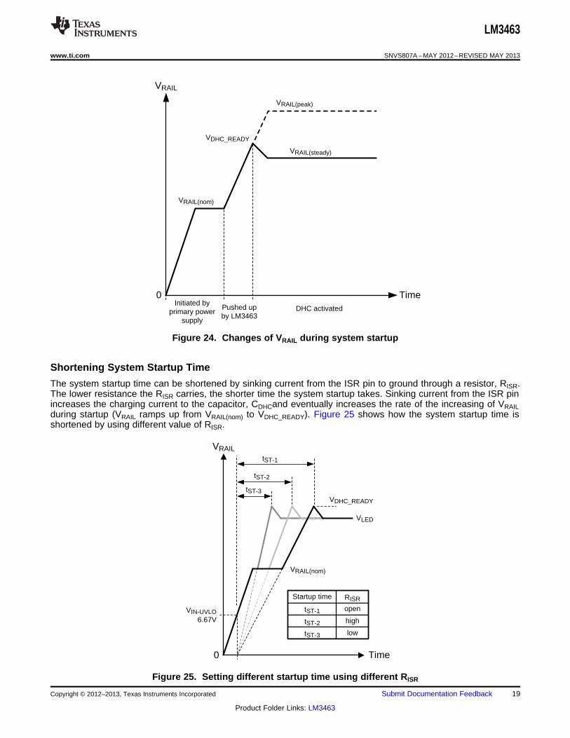
System Startup
When the LM3463 is powered, the internal Operational Transconductance Amplifier (OTA) charges the capacitorCDHC through the CDHC pin. As the voltage at the CDHC pin increases, the voltage at the OutP pin starts toreduce from VCC. When the voltage of the OutP pin falls below VFB + 0.7V, the OutP pin sinks current from theVFB node and eventually pulls up the output voltage of the primary power supply (VRAIL). As the VRAIL reachesVDHC_READY, the LM3463 performs a test to identify the status of the LED strings (short / open circuit of LEDstrings). The VDHC_REDAY is defined by an external voltage divider which consists of RFB1 and RFB2. TheVDHC_READY is calculated following the equation:
(7)
After the test is completed, the LM3463 turns on the LED strings with regulated output currents. At the momentthat the LM3463 turns the LEDs on, the OutP pin stops sinking current from the VFB node and in turn VRAIL slewsdown. Along with the decreasing of VRAIL, the voltage at the VDRn pins falls to approach 1V. When a VDRn isdecreased to 1V, the DHC loop enters a steady state to maintain the lowest VDRn to 1V average at a slowmanner defined by CDHC. Figure 24 presents the changes of VRAIL from system power up to DHC loop enterssteady state.
18 Submit Documentation Feedback Copyright © 2012–2013, Texas Instruments Incorporated
Product Folder Links: LM3463
0
VDHC_READY
VRAIL(nom)
VLED
VRAIL
Time
tST-1
tST-2
tST-3
tST-1 open
RISRStartup time
tST-2 high
tST-3 low
VIN-UVLO6.67V
0
VDHC_READY
VRAIL(nom)
VRAIL(steady)
VRAIL(peak)
VRAIL
TimePushed up by LM3463
Initiated by primary power
supply
DHC activated
LM3463
www.ti.com SNVS807A –MAY 2012–REVISED MAY 2013
Figure 24. Changes of VRAIL during system startup
Shortening System Startup Time
The system startup time can be shortened by sinking current from the ISR pin to ground through a resistor, RISR.The lower resistance the RISR carries, the shorter time the system startup takes. Sinking current from the ISR pinincreases the charging current to the capacitor, CDHCand eventually increases the rate of the increasing of VRAILduring startup (VRAIL ramps up from VRAIL(nom) to VDHC_READY). Figure 25 shows how the system startup time isshortened by using different value of RISR.
Figure 25. Setting different startup time using different RISR
Copyright © 2012–2013, Texas Instruments Incorporated Submit Documentation Feedback 19
Product Folder Links: LM3463
LM3463
SNVS807A –MAY 2012–REVISED MAY 2013 www.ti.com
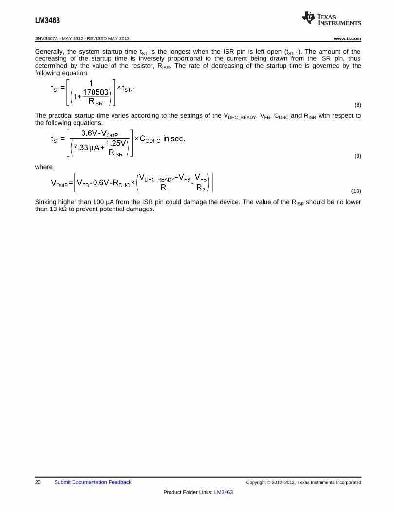
Generally, the system startup time tST is the longest when the ISR pin is left open (tST-1). The amount of thedecreasing of the startup time is inversely proportional to the current being drawn from the ISR pin, thusdetermined by the value of the resistor, RISR. The rate of decreasing of the startup time is governed by thefollowing equation.
(8)
The practical startup time varies according to the settings of the VDHC_READY, VFB, CDHC and RISR with respect tothe following equations.
(9)
where
(10)
Sinking higher than 100 µA from the ISR pin could damage the device. The value of the RISR should be no lowerthan 13 kΩ to prevent potential damages.
20 Submit Documentation Feedback Copyright © 2012–2013, Texas Instruments Incorporated
Product Folder Links: LM3463
VLED-MAX-COLD, the highest forward voltage of LED strings under low temperature
Identify VLED-MAX-COLD
Identify VLED-MIN-HOT
Adjust the nominal output voltage of the primary power supply,
VRAIL(nom) = VLED-MIN-HOT - 5V
Set the peak output voltage of the primary
power supply (at VOutP = 0.15V),
VRAIL(peak) = VLED-MAX-COLD + 10V
Set the LED turn on voltage,
VDHC_READY = VLED-MAX-COLD + 5V
Begin design
End of design
VLED-MIN-HOT, the lowest forward voltage of LED strings under high temperature
VRAIL(nom), the nominal output voltage of the primary power supply.
e.g. Assume VFB = 2.5V,
REMARKSPROCEDURES
VRAIL(peak), the output voltage of the primary power supply when the OutP pin is pulling to its minimum.
VFB
R2
VFB - 0.15 - 0.6
RDHCVFBR1VRAIL(peak) =
R1 + R2
R2
2.5VVRAIL(nom) =
VDHC_READY, the LED turn on voltage is
defined by RFB1 and RFB2 connected to the VLedFB pin.
RFB1 + RFB2
RFB22.5VVDHC_READY =
LM3463
www.ti.com SNVS807A –MAY 2012–REVISED MAY 2013
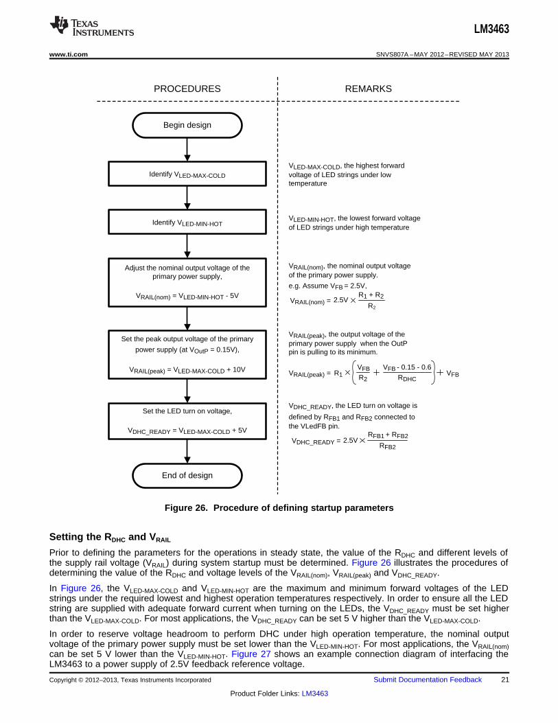
Figure 26. Procedure of defining startup parameters
Setting the RDHC and VRAIL
Prior to defining the parameters for the operations in steady state, the value of the RDHC and different levels ofthe supply rail voltage (VRAIL) during system startup must be determined. Figure 26 illustrates the procedures ofdetermining the value of the RDHC and voltage levels of the VRAIL(nom), VRAIL(peak) and VDHC_READY.
In Figure 26, the VLED-MAX-COLD and VLED-MIN-HOT are the maximum and minimum forward voltages of the LEDstrings under the required lowest and highest operation temperatures respectively. In order to ensure all the LEDstring are supplied with adequate forward current when turning on the LEDs, the VDHC_READY must be set higherthan the VLED-MAX-COLD. For most applications, the VDHC_READY can be set 5 V higher than the VLED-MAX-COLD.
In order to reserve voltage headroom to perform DHC under high operation temperature, the nominal outputvoltage of the primary power supply must be set lower than the VLED-MIN-HOT. For most applications, the VRAIL(nom)can be set 5 V lower than the VLED-MIN-HOT. Figure 27 shows an example connection diagram of interfacing theLM3463 to a power supply of 2.5V feedback reference voltage.
Copyright © 2012–2013, Texas Instruments Incorporated Submit Documentation Feedback 21
Product Folder Links: LM3463

VRAIL(peak) is the highest output voltage that the power converter needs to deliver.
ILEDx is the forward current of an LED string.
Determine:
ILEDx, VRAIL(peak) and VRAIL(nom)
Prepare a power converter which has a
maximum output power > POUT(nom) and a
maximum output voltage > VRAIL(peak)
Adjust R1 and R2 to reduce the nominal output voltage of the power converter to
VRAIL(nom)
Begin powersupply selection
The power converter must be able to
deliver a power no less than PRAIL(peak)
even if the VRAIL is pushed to the
maximum by the LM3463, VRAIL(peak)
REMARKSPROCEDURES
Adjust the value of R1 and R2 so as to meet the equation:
VFBR2
VRAIL(nom) =
Calculate the required maximum output
Power, PRAIL(peak) of the power supply
End of powersupply selection
ILEDxNo. of
output ch. PRAIL(peak) = VRAIL(peak)
R1 + R2
2.5V
To control circuit of primary power supply
VFB
R1
R2
VRAIL
GND
OutP
VIN
GND REFRTN
RDHC
Primary power supply
LM3463
RFB1
RFB2
VLedFB
LM3463
SNVS807A –MAY 2012–REVISED MAY 2013 www.ti.com
Figure 27. Connecting the LM3463 to a power supply
Figure 28. Procedures of selecting the primary power supply
22 Submit Documentation Feedback Copyright © 2012–2013, Texas Instruments Incorporated
Product Folder Links: LM3463

VDRn
VSEnVDRx = VDRVLIM x 4
LM3463
www.ti.com SNVS807A –MAY 2012–REVISED MAY 2013
Choosing the proper Primary Power Supply
If the primary power supply is an off-the-shelf power converter, it is essential to make certain that the powerconverter is able to withstand the VRAIL(peak). In order to allow DHC, the nominal output voltage of the primarypower supply needs to be adjusted to below VLED-MIN-HOT as well. The suggested procedures for selecting theproper power supply are as shown in Figure 28.
Selection of External MOSFET
The selection of external MOSFET is dependent on the highest current and the highest voltage that could beapplied to the drain terminal of the MOSFET. Generally, the Drain-to-Source breakdown voltage (VDSS) and thecontinuous drain current (ID) of the external MOSFET must be higher than the defined peak supply rail voltage(VRAIL(peak)) and the maximum output LED current (IOUTn) respectively.
Testing LEDs at System Startup
As VRAIL increases to VDHC_READY, the voltage at the VLedFB pin equals 2.5V. When the voltage at the VLedFBpin rises to 2.5V, the LM3463 sinks 100 µA through every LED strings from the supply rail into the DRn pins forcertain period of time to determine the status of the LED strings. The time for checking LED strings is defined bythe value of the external capacitor, CFLT and is governed by the following equation:
(11)
If the voltage at any DRn pin is detected lower than 350 mV in the LED test period, that particular output channelwill be disabled and excluded from the DHC loop. All disabled output channels will remain in OFF state until asystem restarting is undertaken. The LED test performs only once after the voltage at VLedFB pin hits 2.5V. Thedisabled channel can be re-enabled by pulling the EN pin to GND for 10 ms (issuing a system restart) or re-powering the entire system.
MOSFET Power Dissipation Limit
In order to protect the MOSFETs from thermal break down when a short circuit of the LED sting(s) isencountered, the LM3463 reduces the output current according to the increment of the drain voltage of theMOSFET (VDRn) when the drain voltage exceeds a certain preset threshold voltage to limit the power dissipationon the MOSFETs. This threshold voltage is defined by the voltage being applied to the DRVLIM pin, VDRVLIM andis roughly four times the voltage of the VDRVLIM. For example, if the desired drain threshold voltage to performoutput current reduction is 16V, the DRVLIM pin voltage should be biased to 4V. Figure 29 shows the relationbetween VSEn, VDRn and VDRVLIM.
Figure 29. VSEn reduces as VDRn exceeds VDRVLIM x4
Copyright © 2012–2013, Texas Instruments Incorporated Submit Documentation Feedback 23
Product Folder Links: LM3463
VCC Regulator
LM3463
GND
47 k
VCC
BUF
GND
DIMnO/P
GND
External PWM signal source
(e.g. MCU)
BUF To dimming control circuit
PWM signal
RPU
Open-drain output
2 M
LM3463
SNVS807A –MAY 2012–REVISED MAY 2013 www.ti.com
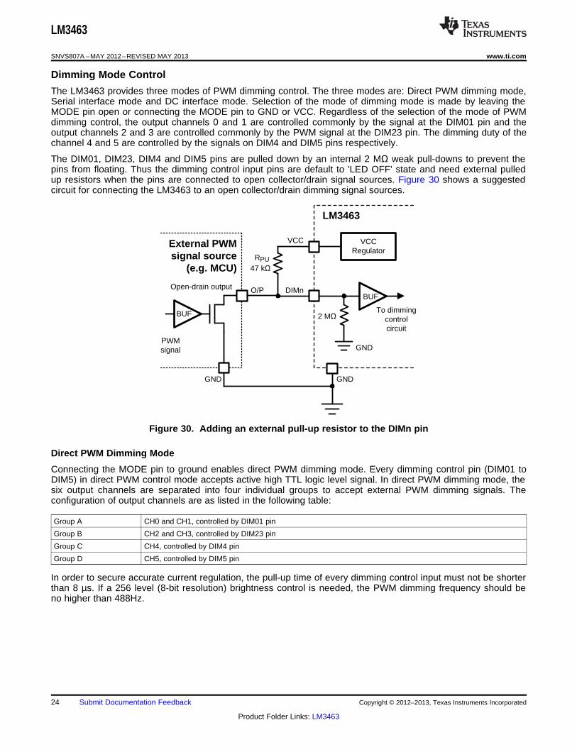
Dimming Mode Control
The LM3463 provides three modes of PWM dimming control. The three modes are: Direct PWM dimming mode,Serial interface mode and DC interface mode. Selection of the mode of dimming mode is made by leaving theMODE pin open or connecting the MODE pin to GND or VCC. Regardless of the selection of the mode of PWMdimming control, the output channels 0 and 1 are controlled commonly by the signal at the DIM01 pin and theoutput channels 2 and 3 are controlled commonly by the PWM signal at the DIM23 pin. The dimming duty of thechannel 4 and 5 are controlled by the signals on DIM4 and DIM5 pins respectively.
The DIM01, DIM23, DIM4 and DIM5 pins are pulled down by an internal 2 MΩ weak pull-downs to prevent thepins from floating. Thus the dimming control input pins are default to 'LED OFF' state and need external pulledup resistors when the pins are connected to open collector/drain signal sources. Figure 30 shows a suggestedcircuit for connecting the LM3463 to an open collector/drain dimming signal sources.
Figure 30. Adding an external pull-up resistor to the DIMn pin
Direct PWM Dimming Mode
Connecting the MODE pin to ground enables direct PWM dimming mode. Every dimming control pin (DIM01 toDIM5) in direct PWM control mode accepts active high TTL logic level signal. In direct PWM dimming mode, thesix output channels are separated into four individual groups to accept external PWM dimming signals. Theconfiguration of output channels are as listed in the following table:
Group A CH0 and CH1, controlled by DIM01 pin
Group B CH2 and CH3, controlled by DIM23 pin
Group C CH4, controlled by DIM4 pin
Group D CH5, controlled by DIM5 pin
In order to secure accurate current regulation, the pull-up time of every dimming control input must not be shorterthan 8 µs. If a 256 level (8-bit resolution) brightness control is needed, the PWM dimming frequency should beno higher than 488Hz.
24 Submit Documentation Feedback Copyright © 2012–2013, Texas Instruments Incorporated
Product Folder Links: LM3463

LM3463
www.ti.com SNVS807A –MAY 2012–REVISED MAY 2013
Serial Interface Mode
Leaving MODE pin floating enables serial interface mode. In serial interface mode, the DIM01, DIM23 and DIM4pins are used together as a serial data interface to accept external dimming control data frames serially. Thefollowing table presents the functions of the DIM01, DIM23 and DIM4 pins in serial interface mode:
DIM01 Serial data packet input (8-bit packet size)
DIM23 Clock signal input for data bit latching
DIM4 End Of Frame (EOF) signal input for data packet loading
The DIM5 pin is not used in this mode and should connect to GND. Every data frame contains four 8–bit widedata byte for PWM dimming control. Every data byte controls the PWM dimming duty of its corresponding outputchannel(s): A hexadecimal 000h gives 0% dimming duty; a hexadecimal 0FFh gives 100% dimming duty.Respectively, the first byte being loaded into the LM3463 controls the dimming duty of CH0 and CH1, the secondbyte controls the dimming duty of CH2 and CH3, the third byte controls the dimming duty of CH4 and the forthbyte controls the dimming duty of CH5.
In serial interface mode, the six output channels are separated into four individual groups as listed in thefollowing table:
Group A CH0 and CH1, controlled by the first byte
Group B CH2 and CH3, controlled by the second byte
Group C CH4, controlled by the third byte
Group D controlled by the forth byte
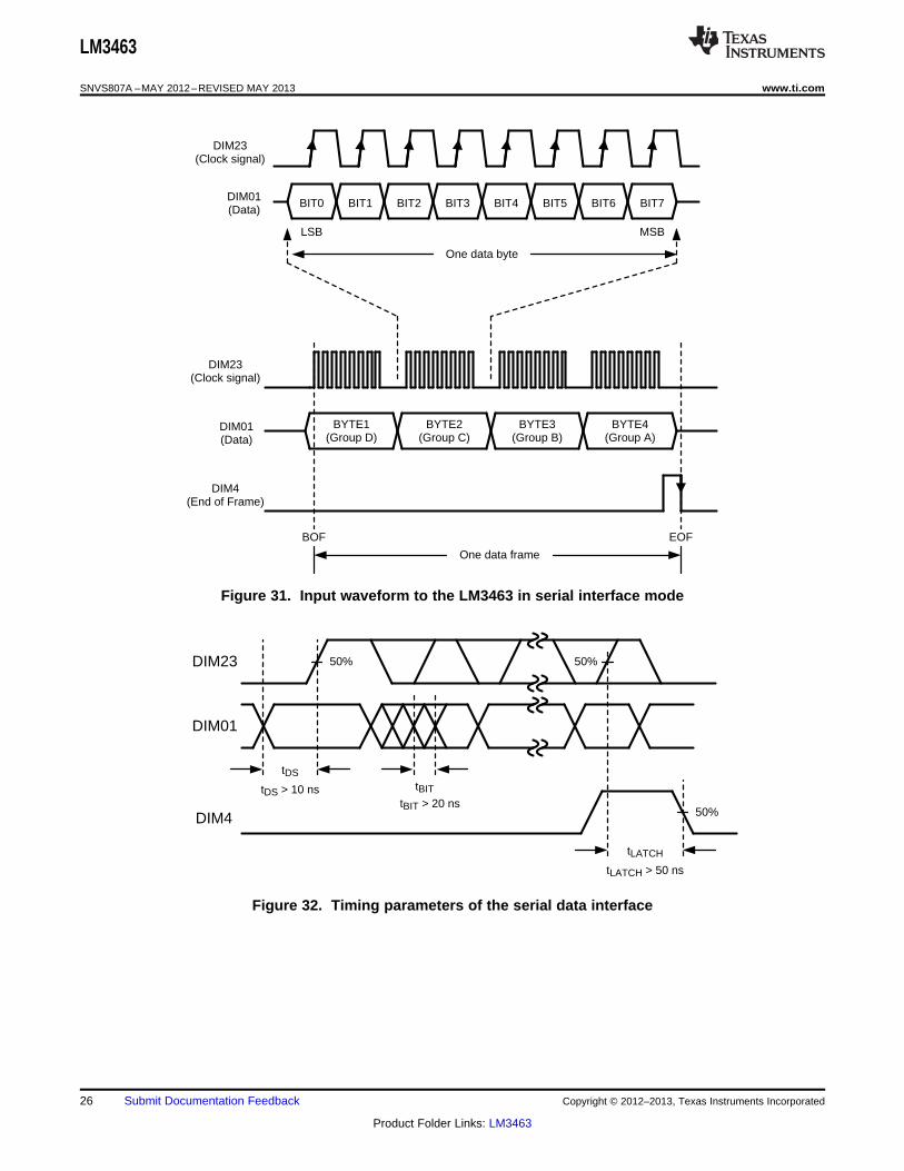
A data bit is latched into the LM3463 by applying a rising edge to the DIM02 pin. After clocking 32 bits (4 databytes) into the LM3463, a falling edge should be applied to the DIM4 pin to indicate an EOF and load data bytesfrom data buffer to output channels accordingly. Figure 31 shows the serial input waveforms to the LM3463 tofacilitate in serial interface mode. Figure 32 shows the timing parameters of the serial data interface. The PWMdimming duty in the serial interface mode is governed by the following equation:
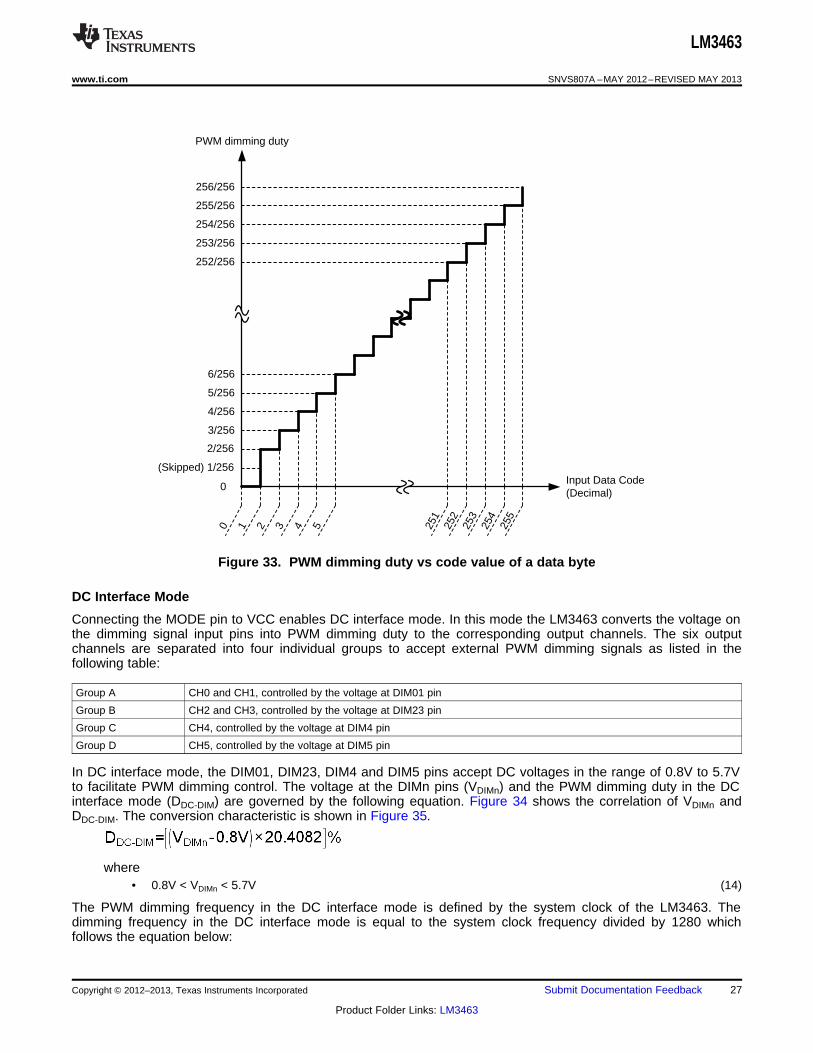
(12)
The PWM dimming duty at decimal data codes 01 (001h) and 02 (002h) are rounded up to 2/256. Thus theminimum dimming duty in the serial interface mode is 2/256 or 0.781%. Figure 33 shows the relationship of thePWM dimming duty and the code value of a data byte in the serial interface mode. The PWM dimming frequencyin serial interface mode is defined by the system clock of the LM3463. The dimming frequency in the serialinterface mode is equal to the system clock frequency divided by 256 which follows the equation below:
(13)
In order to achieve a 256 level (8–bit resolution) brightness control, the minimum on time of every channel(1/(fSERIAL-DIM*256)) should be no shorter than 8us, thus a dimming frequency of 488Hz is suggested to use.
Copyright © 2012–2013, Texas Instruments Incorporated Submit Documentation Feedback 25
Product Folder Links: LM3463
50%
tDS
DIM01
DIM23
tDS > 10 ns tBIT
tBIT > 20 ns50%
tLATCH
50%
tLATCH > 50 ns
DIM4
BIT7BIT6BIT5BIT4BIT3BIT2BIT1BIT0
One data byte
DIM01
DIM23(Clock signal)
(Data)
DIM01
DIM23(Clock signal)
(Data)BYTE1
(Group D)BYTE2
(Group C)BYTE3
(Group B)BYTE4
(Group A)
DIM4(End of Frame)
EOF
One data frame
LSB MSB
BOF
LM3463
SNVS807A –MAY 2012–REVISED MAY 2013 www.ti.com
Figure 31. Input waveform to the LM3463 in serial interface mode
Figure 32. Timing parameters of the serial data interface
26 Submit Documentation Feedback Copyright © 2012–2013, Texas Instruments Incorporated
Product Folder Links: LM3463
Input Data Code (Decimal)
3/256
PWM dimming duty
4/256
5/256
0
6/256
32 41 5 254
253
255
252
0
256/256
251
255/256
254/256
253/256
252/256
(Skipped) 1/256
2/256
LM3463
www.ti.com SNVS807A –MAY 2012–REVISED MAY 2013
Figure 33. PWM dimming duty vs code value of a data byte
DC Interface Mode
Connecting the MODE pin to VCC enables DC interface mode. In this mode the LM3463 converts the voltage onthe dimming signal input pins into PWM dimming duty to the corresponding output channels. The six outputchannels are separated into four individual groups to accept external PWM dimming signals as listed in thefollowing table:
Group A CH0 and CH1, controlled by the voltage at DIM01 pin
Group B CH2 and CH3, controlled by the voltage at DIM23 pin
Group C CH4, controlled by the voltage at DIM4 pin
Group D CH5, controlled by the voltage at DIM5 pin
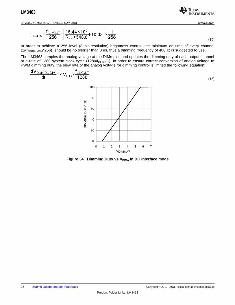
In DC interface mode, the DIM01, DIM23, DIM4 and DIM5 pins accept DC voltages in the range of 0.8V to 5.7Vto facilitate PWM dimming control. The voltage at the DIMn pins (VDIMn) and the PWM dimming duty in the DCinterface mode (DDC-DIM) are governed by the following equation. Figure 34 shows the correlation of VDIMn andDDC-DIM. The conversion characteristic is shown in Figure 35.
where• 0.8V < VDIMn < 5.7V (14)
The PWM dimming frequency in the DC interface mode is defined by the system clock of the LM3463. Thedimming frequency in the DC interface mode is equal to the system clock frequency divided by 1280 whichfollows the equation below:
Copyright © 2012–2013, Texas Instruments Incorporated Submit Documentation Feedback 27
Product Folder Links: LM3463
0 1 2 3 4 5 6 7
0
20
40
60
80
100D
IMM
ING
DU
TY
(%
)
VDIMn(V)
LM3463
SNVS807A –MAY 2012–REVISED MAY 2013 www.ti.com
(15)
In order to achieve a 256 level (8–bit resolution) brightness control, the minimum on time of every channel(1/(fSERIAL-DIM*256)) should be no shorter than 8 us, thus a dimming frequency of 488Hz is suggested to use.
The LM3463 samples the analog voltage at the DIMn pins and updates the dimming duty of each output channelat a rate of 1280 system clock cycle (1280/fCLKOUT). In order to ensure correct conversion of analog voltage toPWM dimming duty, the slew rate of the analog voltage for dimming control is limited the following equation:
(16)
Figure 34. Dimming Duty vs VDIMn in DC interface mode
28 Submit Documentation Feedback Copyright © 2012–2013, Texas Instruments Incorporated
Product Folder Links: LM3463

Analog voltageat the DIMn pin
(Skipped) 1/256
PWM dimming duty
3/256
4/256
0
5/256
5.7V
-VLS
B
5.7V
-2V LS
B5.
7V
5.7V
-3V LS
B
256/256
5.7V
-4V LS
B
255/256
254/256
253/256
252/2560.
8V+3
V LSB
0.8V
+2V LS
B0.
8V+4
V LSB
0.8V
+VLS
B
0.8V
6/256
VLSB =5.7V - 0.8V
256
2/256
LM3463
www.ti.com SNVS807A –MAY 2012–REVISED MAY 2013
Figure 35. Conversion characteristic of the analog voltage to PWM dimming control circuit
Using Less than Six Output Channels
If less than 6 output channels are needed, the unused output channel(s) of the LM3463 can be disabled by notinstalling the external MOSFET and current sensing resistor. The drain voltage sensing pin (DRn), gate driveroutput pin (GDn) and current sensing input pin (SEn) of a disabled channel must be left floating to secure properoperation. The output channel(s) which has no external MOSFET and current sensing resistor installed isdisabled and excluded from DHC loop at system startup while the VRAIL reaches VDHC_READY.
A total of five output channels of the LM3463 can be disabled. The channel 0 must be in use regardless of thenumber of disabled channel. This feature also applies in cascade operation.
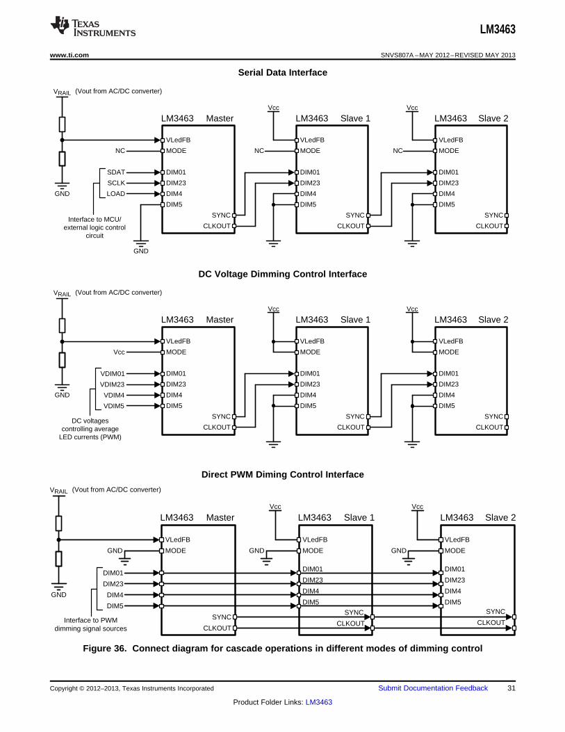
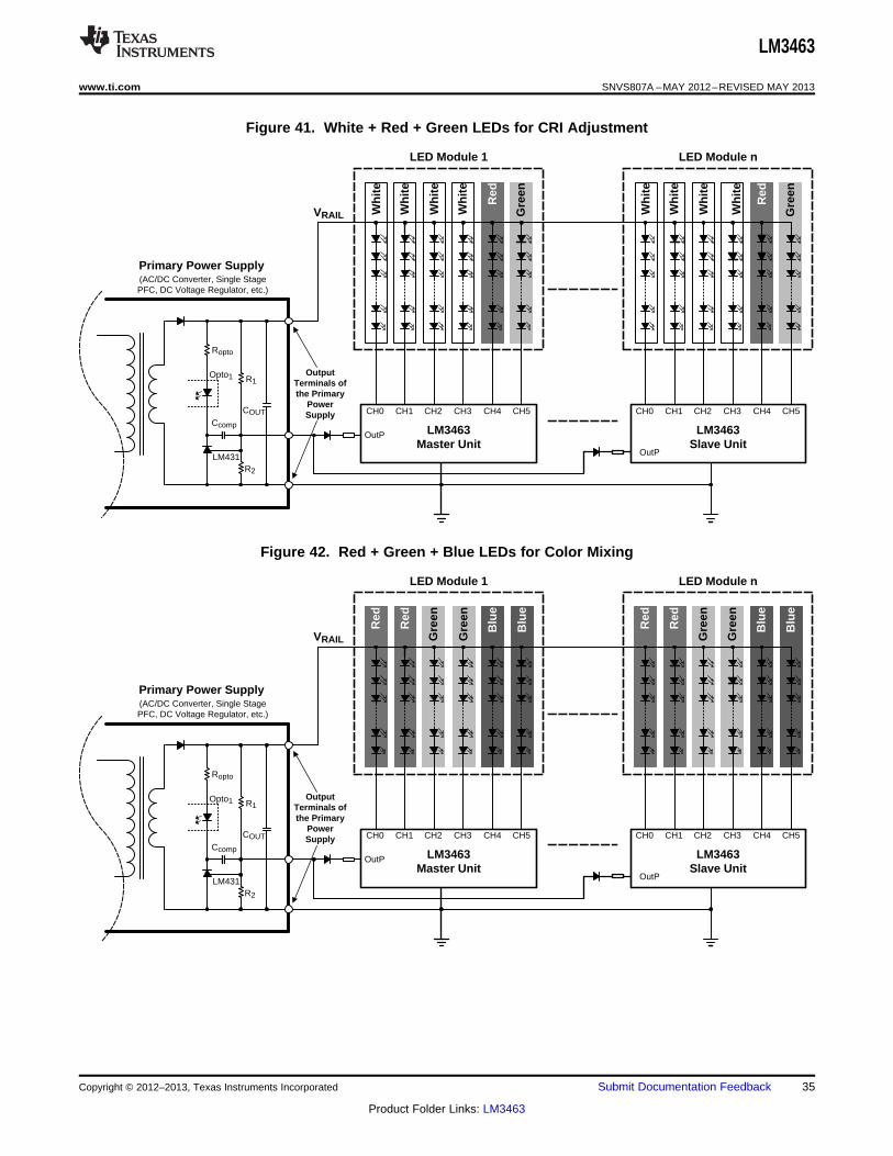
Cascading of LM3463
For the applications that require more than six output channels, two or more pieces of LM3463 can be cascadedto expand the number of output channel. Dimming control is allowed in cascade operation. The connectiondiagrams for cascade operation in different modes of dimming control are as shown in Figure 36.
Serial interface mode in cascade operation
In the serial interface mode, the master LM3463 accepts external data frames through the serial data interfacewhich consists of the DIM01, DIM23 and DIM4 pins and passes the frames to the following slave LM3463through its serial data output interface (SYNC and CLKOUT pins). Every slave unit shifts data in and out bit bybit to its following slave unit.
Copyright © 2012–2013, Texas Instruments Incorporated Submit Documentation Feedback 29
Product Folder Links: LM3463

LM3463
SNVS807A –MAY 2012–REVISED MAY 2013 www.ti.com
DC interface mode in cascade operation
In the DC interface mode, the master unit accepts four individual analog dimming control signals from externalsignal sources (via the DIM01, DIM23, DIM4 and DIM5 pins) and encodes the analog signals into 8-bit serialdimming control signals. The master LM3463 passes the encoded dimming control signals serially to thefollowing slave unit through its serial data output interface (SYNC and CLKOUT pins). Every slave unit shifts datain and out bit by bit to its following slave unit.
Direct PWM dimming mode in cascade operation
In the Direct PWM Dimming mode, the master and slave units share the PWM dimming control signals at theDIM01, DIM23, DIM4 and DIM5 pin to facilitate dimming control. In this mode, the SYNC and CLKOUT of allslave units should be connected to the SYNC and CLKOUT pin of the master unit accordingly to perform startupsynchronization. Since the dimming control signal inputs of all the LM3464 are connected in parallel to share thecontrol signals, it is essential to ensure the signal source is strong enough to drive all the LM3463 in parallel.
30 Submit Documentation Feedback Copyright © 2012–2013, Texas Instruments Incorporated
Product Folder Links: LM3463
DIM01
DIM23
DIM4
DIM5
VLedFB
MODE
SYNC
CLKOUT
LM3463 Master
DIM01
DIM23
DIM4
DIM5
VLedFB
MODE
SYNC
CLKOUT
LM3463 Slave 1Vcc
GND
DIM01
DIM23
DIM4
DIM5
VLedFB
MODE
SYNC
CLKOUT
LM3463 Slave 2Vcc
GNDGND
GND
VRAIL
Interface to PWM dimming signal sources
(Vout from AC/DC converter)
DIM01
DIM23
DIM4
DIM5
VLedFB
MODE
SYNC
CLKOUT
LM3463 Master
DIM01
DIM23
DIM4
DIM5
VLedFB
MODE
SYNC
CLKOUT
LM3463 Slave 1Vcc
DIM01
DIM23
DIM4
DIM5
VLedFB
MODE
SYNC
CLKOUT
LM3463 Slave 2Vcc
GND
VRAIL (Vout from AC/DC converter)
Vcc
VDIM01
VDIM23
VDIM4
VDIM5
DC voltages controlling average
LED currents (PWM)
DIM01
DIM23
DIM4
DIM5
VLedFB
MODE
SYNC
CLKOUT
LM3463 Master
DIM01
DIM23
DIM4
DIM5
VLedFB
MODE
SYNC
CLKOUT
LM3463 Slave 1Vcc
NC
DIM01
DIM23
DIM4
DIM5
VLedFB
MODE
SYNC
CLKOUT
LM3463 Slave 2Vcc
NC
SDAT
SCLK
LOAD
GND
NC
GND
VRAIL
Interface to MCU/external logic control
circuit
(Vout from AC/DC converter)
LM3463
www.ti.com SNVS807A –MAY 2012–REVISED MAY 2013
Serial Data Interface
DC Voltage Dimming Control Interface
Direct PWM Diming Control Interface
Figure 36. Connect diagram for cascade operations in different modes of dimming control
Copyright © 2012–2013, Texas Instruments Incorporated Submit Documentation Feedback 31
Product Folder Links: LM3463
DR0
GD0
OutP
REFRTN
VIN
DR1
DR5
Primary power supply
Voltage feedback pin
Voltage output
High Power LED Arrays
Q1
RDHC
GND
GND
RISNS1
RISNS2
RISNS6
GND GND
Q2
Q6
GD1
SE0
Faultb
D1
VIN
LED1 LED2 LED6
VRAIL
U1
LM3463
SE1
SE5
GD5
REFRTN
CVCC
Vcc
VREF
IOUTADJ
GND
CFLTCDHC
RIBIAS FCAP
CDHC
ISR
RFS
FS
DRVLIM
RLMT2
RLMT1
VCC
MODE
DIM01
DIM23
DIM4
DIM5
EN
RFB1
RFB2
CIN
VLedFB
REFRTN
GND
GND
Faultb
MODE
DIM01
DIM23
DIM4
DIM5
EN
CLKOUT SYNC
Connections for cascade operation
PWM dimming signal inputs
CVREF
LM3463
SNVS807A –MAY 2012–REVISED MAY 2013 www.ti.com
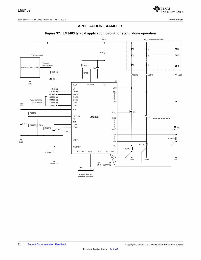
APPLICATION EXAMPLES
Figure 37. LM3463 typical application circuit for stand alone operation
32 Submit Documentation Feedback Copyright © 2012–2013, Texas Instruments Incorporated
Product Folder Links: LM3463

DR0
GD0
OutP
REFRTN
VIN
DR1
DR5
Primary power supply
Voltage feedback pin
Voltage output
High Power LED Arrays
Q1
RDHC
GND
GND
RISNS1
RISNS2
RISNS6
GND GND
Q2
Q6
GD1
SE0
Faultb
D1
VIN
LED1 LED2 LED6
VRAIL
U1
LM3463
SE1
SE5
GD5
REFRTN
RIADJ2
RIADJ1
CVCC
Vcc
VREF
IOUTADJ
GND
CFLTCDHC
RIBIAS FCAP
CDHC
ISR
RFS
FS
DRVLIM
RLMT2
RLMT1
VCC
EN
RFB1
RFB2
CIN
VLedFB
REFRTN
GND
GND
Faultb
MODE
DIM01
DIM23
DIM4
DIM5
EN
CLKOUT SYNC
Connections for cascade operation
CVREF
GND
LM3463
www.ti.com SNVS807A –MAY 2012–REVISED MAY 2013
Figure 38. LM3463 typical application circuit for true analog dimming control
Copyright © 2012–2013, Texas Instruments Incorporated Submit Documentation Feedback 33
Product Folder Links: LM3463

Wh
ite
Am
ber
Wh
ite
Wh
ite
Wh
ite
Wh
ite
Am
ber
Wh
ite
CH0 CH1 CH2 CH3 CH4 CH5COUT
R1
R2
Ropto
Opto1
Ccomp
LM431
(AC/DC Converter, Single StagePFC, DC Voltage Regulator, etc.)
Primary Power Supply
LED Module 1
LM3463Master Unit
OutP
VRAIL
Output Terminals of the Primary
Power Supply
Wh
ite
Wh
ite
Wh
ite
Wh
ite
LED Module n
LM3463Slave Unit
OutP
CH0 CH1 CH2 CH3 CH4 CH5
Wh
ite
Wh
ite
Wh
ite
Wh
ite
Wh
ite
Wh
ite
Wh
ite
Wh
ite
CH0 CH1 CH2 CH3 CH4 CH5COUT
R1
R2
Ropto
Opto1
Ccomp
LM431
(AC/DC Converter, Single StagePFC, DC Voltage Regulator, etc.)
Primary Power Supply
LED Module 1
LM3463Master Unit
OutP
VRAIL
Output Terminals of the Primary
Power Supply
Wh
ite
Wh
ite
Wh
ite
Wh
ite
LED Module n
LM3463Slave Unit
OutP
CH0 CH1 CH2 CH3 CH4 CH5
LM3463
SNVS807A –MAY 2012–REVISED MAY 2013 www.ti.com
Figure 39. White LEDs Only
Figure 40. White + Amber LEDs for Color Temperature Adjustment
34 Submit Documentation Feedback Copyright © 2012–2013, Texas Instruments Incorporated
Product Folder Links: LM3463
Red
Gre
en
Blu
e
Blu
e
Red
Gre
en
Red
Gre
en
Blu
e
Blu
e
Red
Gre
en
CH0 CH1 CH2 CH3 CH4 CH5COUT
R1
R2
Ropto
Opto1
Ccomp
LM431
(AC/DC Converter, Single StagePFC, DC Voltage Regulator, etc.)
Primary Power Supply
LED Module 1
LM3463Master Unit
OutP
VRAIL
Output Terminals of the Primary
Power Supply
LED Module n
LM3463Slave Unit
OutP
CH0 CH1 CH2 CH3 CH4 CH5
Red
Gre
en
Wh
ite
Wh
ite
Wh
ite
Red
Gre
en
Wh
ite
CH0 CH1 CH2 CH3 CH4 CH5COUT
R1
R2
Ropto
Opto1
Ccomp
LM431
(AC/DC Converter, Single StagePFC, DC Voltage Regulator, etc.)
Primary Power Supply
LED Module 1
LM3463Master Unit
OutP
VRAIL
Output Terminals of the Primary
Power Supply
Wh
ite
Wh
ite
Wh
ite
Wh
ite
LED Module n
LM3463Slave Unit
OutP
CH0 CH1 CH2 CH3 CH4 CH5
LM3463
www.ti.com SNVS807A –MAY 2012–REVISED MAY 2013
Figure 41. White + Red + Green LEDs for CRI Adjustment
Figure 42. Red + Green + Blue LEDs for Color Mixing
Copyright © 2012–2013, Texas Instruments Incorporated Submit Documentation Feedback 35
Product Folder Links: LM3463
LM3463
SNVS807A –MAY 2012–REVISED MAY 2013 www.ti.com
REVISION HISTORY
Changes from Original (May 2013) to Revision A Page
• Changed layout of National Data Sheet to TI format .......................................................................................................... 35
36 Submit Documentation Feedback Copyright © 2012–2013, Texas Instruments Incorporated
Product Folder Links: LM3463
PACKAGE OPTION ADDENDUM
www.ti.com 10-Dec-2020
Addendum-Page 1
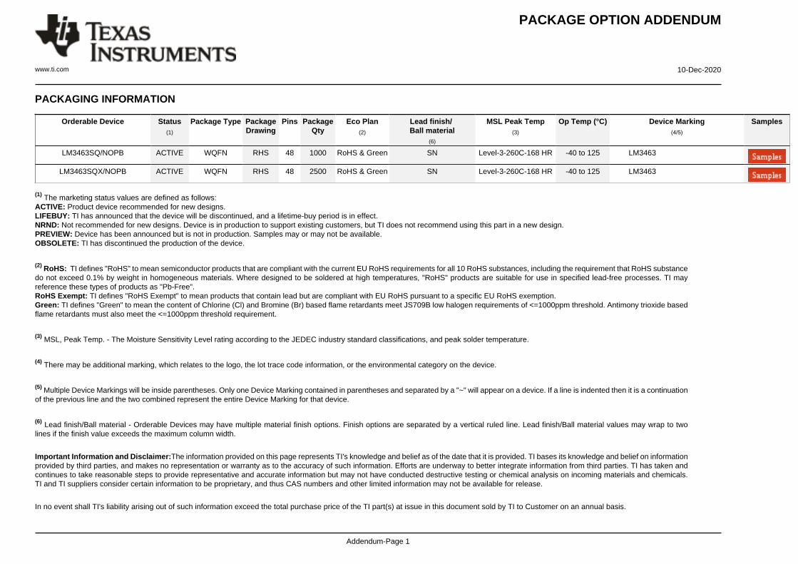
PACKAGING INFORMATION
Orderable Device Status(1)
Package Type PackageDrawing
Pins PackageQty
Eco Plan(2)
Lead finish/Ball material
(6)
MSL Peak Temp(3)
Op Temp (°C) Device Marking(4/5)
Samples
LM3463SQ/NOPB ACTIVE WQFN RHS 48 1000 RoHS & Green SN Level-3-260C-168 HR -40 to 125 LM3463
LM3463SQX/NOPB ACTIVE WQFN RHS 48 2500 RoHS & Green SN Level-3-260C-168 HR -40 to 125 LM3463
(1) The marketing status values are defined as follows:ACTIVE: Product device recommended for new designs.LIFEBUY: TI has announced that the device will be discontinued, and a lifetime-buy period is in effect.NRND: Not recommended for new designs. Device is in production to support existing customers, but TI does not recommend using this part in a new design.PREVIEW: Device has been announced but is not in production. Samples may or may not be available.OBSOLETE: TI has discontinued the production of the device.
(2) RoHS: TI defines "RoHS" to mean semiconductor products that are compliant with the current EU RoHS requirements for all 10 RoHS substances, including the requirement that RoHS substancedo not exceed 0.1% by weight in homogeneous materials. Where designed to be soldered at high temperatures, "RoHS" products are suitable for use in specified lead-free processes. TI mayreference these types of products as "Pb-Free".RoHS Exempt: TI defines "RoHS Exempt" to mean products that contain lead but are compliant with EU RoHS pursuant to a specific EU RoHS exemption.Green: TI defines "Green" to mean the content of Chlorine (Cl) and Bromine (Br) based flame retardants meet JS709B low halogen requirements of <=1000ppm threshold. Antimony trioxide basedflame retardants must also meet the <=1000ppm threshold requirement.
(3) MSL, Peak Temp. - The Moisture Sensitivity Level rating according to the JEDEC industry standard classifications, and peak solder temperature.
(4) There may be additional marking, which relates to the logo, the lot trace code information, or the environmental category on the device.
(5) Multiple Device Markings will be inside parentheses. Only one Device Marking contained in parentheses and separated by a "~" will appear on a device. If a line is indented then it is a continuationof the previous line and the two combined represent the entire Device Marking for that device.
(6) Lead finish/Ball material - Orderable Devices may have multiple material finish options. Finish options are separated by a vertical ruled line. Lead finish/Ball material values may wrap to twolines if the finish value exceeds the maximum column width.
Important Information and Disclaimer:The information provided on this page represents TI's knowledge and belief as of the date that it is provided. TI bases its knowledge and belief on informationprovided by third parties, and makes no representation or warranty as to the accuracy of such information. Efforts are underway to better integrate information from third parties. TI has taken andcontinues to take reasonable steps to provide representative and accurate information but may not have conducted destructive testing or chemical analysis on incoming materials and chemicals.TI and TI suppliers consider certain information to be proprietary, and thus CAS numbers and other limited information may not be available for release.
In no event shall TI's liability arising out of such information exceed the total purchase price of the TI part(s) at issue in this document sold by TI to Customer on an annual basis.
PACKAGE OPTION ADDENDUM
www.ti.com 10-Dec-2020
Addendum-Page 2

TAPE AND REEL INFORMATION
*All dimensions are nominal
Device PackageType
PackageDrawing
Pins SPQ ReelDiameter
(mm)
ReelWidth
W1 (mm)
A0(mm)
B0(mm)
K0(mm)
P1(mm)
W(mm)
Pin1Quadrant
LM3463SQ/NOPB WQFN RHS 48 1000 330.0 16.4 7.3 7.3 1.3 12.0 16.0 Q1
LM3463SQX/NOPB WQFN RHS 48 2500 330.0 16.4 7.3 7.3 1.3 12.0 16.0 Q1
PACKAGE MATERIALS INFORMATION
www.ti.com 21-Oct-2021
Pack Materials-Page 1
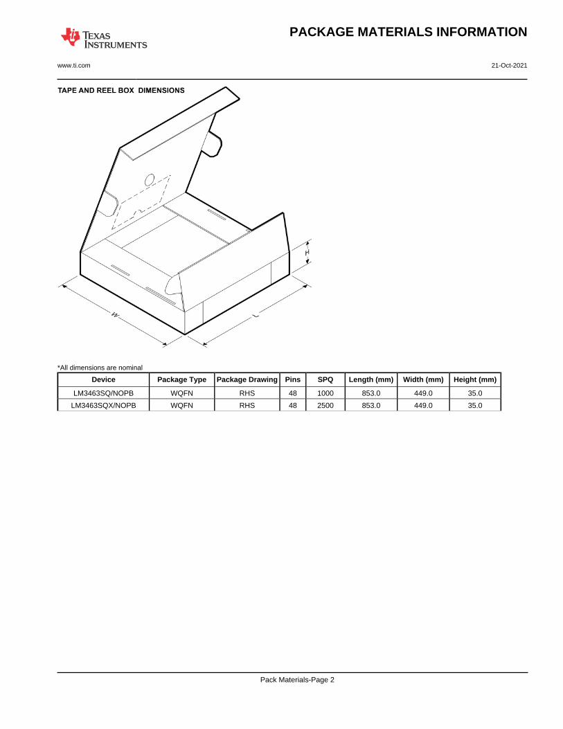
*All dimensions are nominal
Device Package Type Package Drawing Pins SPQ Length (mm) Width (mm) Height (mm)
LM3463SQ/NOPB WQFN RHS 48 1000 853.0 449.0 35.0
LM3463SQX/NOPB WQFN RHS 48 2500 853.0 449.0 35.0
PACKAGE MATERIALS INFORMATION
www.ti.com 21-Oct-2021
Pack Materials-Page 2
www.ti.com
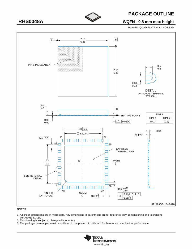
PACKAGE OUTLINE
C
SEE TERMINALDETAIL
48X 0.300.18
5.1 0.1
48X 0.50.3
0.80.7
(A) TYP
0.050.00
44X 0.5
2X5.5
2X 5.5
A 7.156.85
B
7.156.85
0.300.18
0.50.3
(0.2)
WQFN - 0.8 mm max heightRHS0048APLASTIC QUAD FLATPACK - NO LEAD
4214990/B 04/2018
DIM AOPT 1 OPT 2(0.1) (0.2)
PIN 1 INDEX AREA
0.08 C
SEATING PLANE
1
1225
36
13 24
48 37
(OPTIONAL)PIN 1 ID 0.1 C A B
0.05
EXPOSEDTHERMAL PAD
49 SYMM
SYMM
NOTES: 1. All linear dimensions are in millimeters. Any dimensions in parenthesis are for reference only. Dimensioning and tolerancing per ASME Y14.5M. 2. This drawing is subject to change without notice. 3. The package thermal pad must be soldered to the printed circuit board for thermal and mechanical performance.
SCALE 1.800
DETAILOPTIONAL TERMINAL
TYPICAL

www.ti.com
EXAMPLE BOARD LAYOUT
0.07 MINALL AROUND
0.07 MAXALL AROUND
48X (0.25)
48X (0.6)
( 0.2) TYPVIA
44X (0.5)
(6.8)
(6.8)
(1.25) TYP
( 5.1)
(R0.05)TYP
(1.25)TYP
(1.05) TYP
(1.05)TYP
WQFN - 0.8 mm max heightRHS0048APLASTIC QUAD FLATPACK - NO LEAD
4214990/B 04/2018
SYMM
1
12
13 24
25
36
3748
SYMM
LAND PATTERN EXAMPLEEXPOSED METAL SHOWN
SCALE:12X
NOTES: (continued) 4. This package is designed to be soldered to a thermal pad on the board. For more information, see Texas Instruments literature number SLUA271 (www.ti.com/lit/slua271).5. Vias are optional depending on application, refer to device data sheet. If any vias are implemented, refer to their locations shown on this view. It is recommended that vias under paste be filled, plugged or tented.
49
SOLDER MASKOPENING
METAL UNDERSOLDER MASK
SOLDER MASKDEFINED
EXPOSEDMETAL
METAL EDGE
SOLDER MASKOPENING
SOLDER MASK DETAILS
NON SOLDER MASKDEFINED
(PREFERRED)
EXPOSEDMETAL
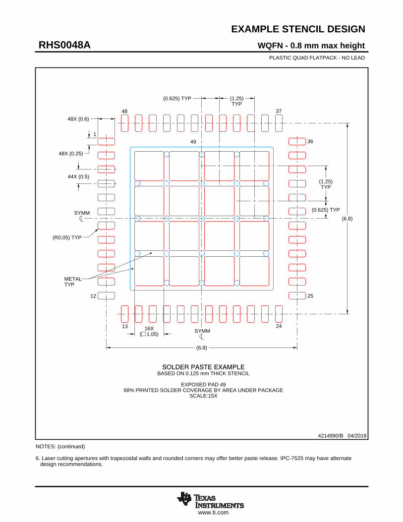
www.ti.com
EXAMPLE STENCIL DESIGN
48X (0.6)
48X (0.25)
44X (0.5)
(6.8)
(6.8)
16X( 1.05)
(0.625) TYP
(R0.05) TYP
(1.25)TYP
(1.25)TYP
(0.625) TYP
WQFN - 0.8 mm max heightRHS0048APLASTIC QUAD FLATPACK - NO LEAD
4214990/B 04/2018
NOTES: (continued) 6. Laser cutting apertures with trapezoidal walls and rounded corners may offer better paste release. IPC-7525 may have alternate design recommendations.
49
SYMM
METALTYP
SOLDER PASTE EXAMPLEBASED ON 0.125 mm THICK STENCIL
EXPOSED PAD 49
68% PRINTED SOLDER COVERAGE BY AREA UNDER PACKAGESCALE:15X
SYMM
1
12
13 24
25
36
3748

IMPORTANT NOTICE AND DISCLAIMERTI PROVIDES TECHNICAL AND RELIABILITY DATA (INCLUDING DATA SHEETS), DESIGN RESOURCES (INCLUDING REFERENCE DESIGNS), APPLICATION OR OTHER DESIGN ADVICE, WEB TOOLS, SAFETY INFORMATION, AND OTHER RESOURCES “AS IS” AND WITH ALL FAULTS, AND DISCLAIMS ALL WARRANTIES, EXPRESS AND IMPLIED, INCLUDING WITHOUT LIMITATION ANY IMPLIED WARRANTIES OF MERCHANTABILITY, FITNESS FOR A PARTICULAR PURPOSE OR NON-INFRINGEMENT OF THIRD PARTY INTELLECTUAL PROPERTY RIGHTS.These resources are intended for skilled developers designing with TI products. You are solely responsible for (1) selecting the appropriate TI products for your application, (2) designing, validating and testing your application, and (3) ensuring your application meets applicable standards, and any other safety, security, regulatory or other requirements.These resources are subject to change without notice. TI grants you permission to use these resources only for development of an application that uses the TI products described in the resource. Other reproduction and display of these resources is prohibited. No license is granted to any other TI intellectual property right or to any third party intellectual property right. TI disclaims responsibility for, and you will fully indemnify TI and its representatives against, any claims, damages, costs, losses, and liabilities arising out of your use of these resources.TI’s products are provided subject to TI’s Terms of Sale or other applicable terms available either on ti.com or provided in conjunction with such TI products. TI’s provision of these resources does not expand or otherwise alter TI’s applicable warranties or warranty disclaimers for TI products.TI objects to and rejects any additional or different terms you may have proposed. IMPORTANT NOTICE
Mailing Address: Texas Instruments, Post Office Box 655303, Dallas, Texas 75265Copyright © 2021, Texas Instruments Incorporated