Embed Size (px)
Citation preview
SN8P2711A 8-Bit Micro-Controller
SONiX TECHNOLOGY CO., LTD Page 1 Version 0.1
SN8P2711A
USER’S MANUAL Version 0.1
SSOONNiiXX 88--BBiitt MMiiccrroo--CCoonnttrroolllleerr
SONIX reserves the right to make change without further notice to any products herein to improve reliability, function or design. SONIX does not assume any liability arising out of the application or use of any product or circuit described herein; neither does it convey any license under its patent rights nor the rights of others. SONIX products are not designed, intended, or authorized for us as components in systems intended, for surgical implant into the body, or other applications intended to support or sustain life, or for any other application in which the failure of the SONIX product could create a situation where personal injury or death may occur. Should Buyer purchase or use SONIX products for any such unintended or unauthorized application. Buyer shall indemnify and hold SONIX and its officers, employees, subsidiaries, affiliates and distributors harmless against all claims, cost, damages, and expenses, and reasonable attorney fees arising out of, directly or indirectly, any claim of personal injury or death associated with such unintended or unauthorized use even if such claim alleges that SONIX was negligent regarding the design or manufacture of the part.
SN8P2711A 8-Bit Micro-Controller
SONiX TECHNOLOGY CO., LTD Page 2 Version 0.1
AMENDENT HISTORY
Version Date Description VER 0.1 Jun. 2007 First issue.
SN8P2711A 8-Bit Micro-Controller
SONiX TECHNOLOGY CO., LTD Page 3 Version 0.1
Table of Content
AMENDENT HISTORY................................................................................................................................ 2
111 PRODUCT OVERVIEW................................................................................................................. 7
1.1 FEATURES........................................................................................................................................ 7 1.2 SYSTEM BLOCK DIAGRAM .......................................................................................................... 9 1.3 PIN ASSIGNMENT ......................................................................................................................... 10 1.4 PIN DESCRIPTIONS....................................................................................................................... 11 1.5 PIN CIRCUIT DIAGRAMS............................................................................................................. 12
222 CENTRAL PROCESSOR UNIT (CPU) ...................................................................................... 14
2.1 MEMORY MAP............................................................................................................................... 14 2.1.1 PROGRAM MEMORY (ROM)............................................................................................... 14
2.1.1.1 RESET VECTOR (0000H) .................................................................................................. 15 2.1.1.2 INTERRUPT VECTOR (0008H)......................................................................................... 16 2.1.1.3 LOOK-UP TABLE DESCRIPTION.................................................................................... 18 2.1.1.4 JUMP TABLE DESCRIPTION ........................................................................................... 20 2.1.1.5 CHECKSUM CALCULATION........................................................................................... 22
2.1.2 CODE OPTION TABLE.......................................................................................................... 23 2.1.3 DATA MEMORY (RAM) ....................................................................................................... 24 2.1.4 SYSTEM REGISTER .............................................................................................................. 25
2.1.4.1 SYSTEM REGISTER TABLE ............................................................................................ 25 2.1.4.2 SYSTEM REGISTER DESCRIPTION ............................................................................... 25 2.1.4.3 BIT DEFINITION of SYSTEM REGISTER....................................................................... 26 2.1.4.4 ACCUMULATOR ............................................................................................................... 27 2.1.4.5 PROGRAM FLAG............................................................................................................... 28 2.1.4.6 PROGRAM COUNTER....................................................................................................... 29 2.1.4.7 Y, Z REGISTERS................................................................................................................. 32 2.1.4.8 R REGISTERS ..................................................................................................................... 33
2.2 ADDRESSING MODE .................................................................................................................... 34 2.2.1 IMMEDIATE ADDRESSING MODE .................................................................................... 34 2.2.2 DIRECTLY ADDRESSING MODE ....................................................................................... 34 2.2.3 INDIRECTLY ADDRESSING MODE ................................................................................... 34
2.3 STACK OPERATION...................................................................................................................... 35 2.3.1 OVERVIEW............................................................................................................................. 35 2.3.2 STACK REGISTERS............................................................................................................... 36 2.3.3 STACK OPERATION EXAMPLE.......................................................................................... 37
333 RESET ............................................................................................................................................. 38
SN8P2711A 8-Bit Micro-Controller
SONiX TECHNOLOGY CO., LTD Page 4 Version 0.1
3.1 OVERVIEW..................................................................................................................................... 38 3.2 POWER ON RESET......................................................................................................................... 39 3.3 WATCHDOG RESET...................................................................................................................... 39 3.4 BROWN OUT RESET ..................................................................................................................... 40
3.4.1 BROWN OUT DESCRIPTION ............................................................................................... 40 3.4.2 THE SYSTEM OPERATING VOLTAGE DECSRIPTION ................................................... 41 3.4.3 BROWN OUT RESET IMPROVEMENT .............................................................................. 41
3.5 EXTERNAL RESET ........................................................................................................................ 44 3.6 EXTERNAL RESET CIRCUIT ....................................................................................................... 44
3.6.1 Simply RC Reset Circuit .......................................................................................................... 44 3.6.2 Diode & RC Reset Circuit ........................................................................................................ 45 3.6.3 Zener Diode Reset Circuit ........................................................................................................ 45 3.6.4 Voltage Bias Reset Circuit ....................................................................................................... 46 3.6.5 External Reset IC...................................................................................................................... 47
444 SYSTEM CLOCK .......................................................................................................................... 48
4.1 OVERVIEW..................................................................................................................................... 48 4.2 CLOCK BLOCK DIAGRAM .......................................................................................................... 48 4.3 OSCM REGISTER........................................................................................................................... 49 4.4 SYSTEM HIGH CLOCK ................................................................................................................. 50
4.4.1 INTERNAL HIGH RC............................................................................................................. 50 4.4.2 EXTERNAL HIGH CLOCK.................................................................................................... 50
4.4.2.1 CRYSTAL/CERAMIC......................................................................................................... 51 4.4.2.2 RC......................................................................................................................................... 51 4.4.2.3 EXTERNAL CLOCK SIGNAL........................................................................................... 52
4.5 SYSTEM LOW CLOCK .................................................................................................................. 53 4.5.1 SYSTEM CLOCK MEASUREMENT .................................................................................... 54
555 SYSTEM OPERATION MODE ................................................................................................... 56
5.1 OVERVIEW..................................................................................................................................... 56 5.2 SYSTEM MODE SWITCHING EXAMPLE................................................................................... 57 5.3 WAKEUP ......................................................................................................................................... 59
5.3.1 OVERVIEW............................................................................................................................. 59 5.3.2 WAKEUP TIME ...................................................................................................................... 59
666 INTERRUPT................................................................................................................................... 60
6.1 OVERVIEW..................................................................................................................................... 60 6.2 INTEN INTERRUPT ENABLE REGISTER................................................................................... 61 6.3 INTRQ INTERRUPT REQUEST REGISTER ................................................................................ 62 6.4 GIE GLOBAL INTERRUPT OPERATION .................................................................................... 63 6.5 PUSH, POP ROUTINE .................................................................................................................... 64
SN8P2711A 8-Bit Micro-Controller
SONiX TECHNOLOGY CO., LTD Page 5 Version 0.1
6.6 INT0 (P0.0) INTERRUPT OPERATION......................................................................................... 65 6.7 INT1 (P0.1) INTERRUPT OPERATION......................................................................................... 67 6.8 TC0 INTERRUPT OPERATION..................................................................................................... 68 6.9 TC1 INTERRUPT OPERATION..................................................................................................... 69 6.10 ADC INTERRUPT OPERATION ................................................................................................... 71 6.11 MULTI-INTERRUPT OPERATION............................................................................................... 72
777 I/O PORT ........................................................................................................................................ 73
7.1 I/O PORT MODE ............................................................................................................................. 73 7.2 I/O PULL UP REGISTER ................................................................................................................ 74 7.3 I/O PORT DATA REGISTER .......................................................................................................... 75 7.4 PORT 4 ADC SHARE PIN............................................................................................................... 76
888 TIMERS .......................................................................................................................................... 80
8.1 WATCHDOG TIMER...................................................................................................................... 80 8.2 TIMER/COUNTER 0 (TC0) ............................................................................................................ 83
8.2.1 OVERVIEW............................................................................................................................. 83 8.2.2 TC0M MODE REGISTER....................................................................................................... 84 8.2.3 TC1X8, TC0X8, TC0GN FLAGS............................................................................................ 85 8.2.4 TC0C COUNTING REGISTER .............................................................................................. 85 8.2.5 TC0R AUTO-LOAD REGISTER............................................................................................ 87 8.2.6 TC0 CLOCK FREQUENCY OUTPUT (BUZZER)................................................................ 88 8.2.7 TC0 TIMER OPERATION SEQUENCE ................................................................................ 89
8.3 TIMER/COUNTER 1 (TC1) ............................................................................................................ 91 8.3.1 OVERVIEW............................................................................................................................. 91 8.3.2 TC1M MODE REGISTER....................................................................................................... 92 8.3.3 TC1X8 FLAG........................................................................................................................... 92 8.3.4 TC1C COUNTING REGISTER .............................................................................................. 93 8.3.5 TC1R AUTO-LOAD REGISTER............................................................................................ 95 8.3.6 TC1 CLOCK FREQUENCY OUTPUT (BUZZER)................................................................ 96 8.3.7 TC1 TIMER OPERATION SEQUENCE ................................................................................ 97
8.4 PWM MODE .................................................................................................................................... 99 8.4.1 OVERVIEW............................................................................................................................. 99 8.4.2 TCnIRQ and PWM Duty........................................................................................................ 100 8.4.3 PWM Duty with TCnR Changing .......................................................................................... 101 8.4.4 PWM PROGRAM EXAMPLE.............................................................................................. 102
999 5+1 CHANNEL ANALOG TO DIGITAL CONVERTER....................................................... 103
9.1 OVERVIEW................................................................................................................................... 103 9.2 ADM REGISTER........................................................................................................................... 104 9.3 ADR REGISTERS.......................................................................................................................... 105
SN8P2711A 8-Bit Micro-Controller
SONiX TECHNOLOGY CO., LTD Page 6 Version 0.1
9.4 ADB REGISTERS.......................................................................................................................... 106 9.5 P4CON REGISTERS ..................................................................................................................... 107 9.6 VREFH REGISTERS..................................................................................................................... 108 9.7 ADC CONVERTING TIME .......................................................................................................... 109 9.8 ADC ROUTINE EXAMPLE.......................................................................................................... 110 9.9 ADC CIRCUIT............................................................................................................................... 112
111000 INSTRUCTION TABLE ..................................................................................................... 113
111111 ELECTRICAL CHARACTERISTIC ................................................................................ 114
11.1 ABSOLUTE MAXIMUM RATING.............................................................................................. 114 11.2 ELECTRICAL CHARACTERISTIC............................................................................................. 114
111222 DEVELOPMENT TOOL VERSION ................................................................................. 117
12.1 ICE (IN CIRCUIT EMULATION)......................................................................................................... 117 12.2 OTP WRITER ................................................................................................................................ 117 12.3 SN8IDE .......................................................................................................................................... 117 12.4 SN8P2711 EV KIT ......................................................................................................................... 118
12.4.1 PCB DESCRIPTION.............................................................................................................. 118 12.4.2 SN8P2711 EV KIT CONNECT TO SN8ICE 2K .................................................................. 120
12.5 TRANSITION BOARD FOR OTP PROGRAMMING ................................................................. 121 12.5.1 SN8P2711 V3 TRANSITION BOARD................................................................................. 121 12.5.2 SN8P2711 MP028A TRANSITION BOARD FOR EZ/MPEZ WRITER ............................ 122 12.5.3 SN8P2711 MP028A CONNECT TO EZ_MP WRITER....................................................... 123 12.5.4 SN8P2711 MP028A CONNECT TO EZ WRITER............................................................... 123 12.5.5 SN8P2711 V3 CONNECT TO EZ WRITER ........................................................................ 124 12.5.6 SN8P2711 V3 CONNECT TO EZ_MP WRITER................................................................. 124
12.6 OTP PROGRAMMING PIN .......................................................................................................... 125 12.6.1 EASY WRITER TRANSITION BOARD SOCKET PIN ASSIGNMENT........................... 125 12.6.2 PROGRAMMING PIN MAPPING: ...................................................................................... 126
111333 PACKAGE INFORMATION ............................................................................................. 127
13.1 P-DIP 14 PIN .................................................................................................................................. 127 13.2 SOP 14 PIN..................................................................................................................................... 128 13.3 SSOP 16 PIN................................................................................................................................... 129
111444 MARKING DEFINITION................................................................................................... 130
14.1 INTRODUCTION.......................................................................................................................... 130 14.2 MARKING INDETIFICATION SYSTEM.................................................................................... 130 14.3 MARKING EXAMPLE ................................................................................................................. 131 14.4 DATECODE SYSTEM .................................................................................................................. 131
SN8P2711A 8-Bit Micro-Controller
SONiX TECHNOLOGY CO., LTD Page 7 Version 0.1
111 PRODUCT OVERVIEW SN8P2711A is modified from SN8P2711. Good internal high RC frequency 16MHz±2%. Good high noisy protecting performance for household application.
SN8P2711 is compatible to SN8P2711A. Better IHRC performance from 16MHz±5% to 16MHz±2%. Good brown out reset production. SN8P2711 code can transfer to SN8P2711A directly. Program the original SN8 of SN8P2711
into SN8P2711A directly without declare SN8P2711A in source code and re-compile again. 1.1 FEATURES
Features Selection Table
Timer PWMCHIP ROM RAM Stack TC0 TC1 I/O ADC Green Mode Buzzer
Wakeup Pin No. Package
SN8P2711 1K*16 64 4 V V 12 5+1 ch V 2 5 P-DIP 14/SOP 14/SSOP 16SN8P2711A 1K*16 64 4 V V 12 5+1 ch V 2 5 P-DIP 14/SOP 14/SSOP 16
♦ Memory configuration ♦ 5+1 channel 12-bit ADC. OTP ROM size: 1K * 16 bits. Five external ADC input RAM size: 64 * 8 bits. One internal battery measurement Internal AD reference voltage (VDD, 4V, 3V ,2V). ♦ Four levels stack buffer. ♦ Two 8-bit Timer/Counter ♦ I/O pin configuration TC0: Auto-reload timer/Counter/PWM0/Buzzer output. Bi-directional: P0, P4, P5. TC1: Auto-reload timer/Counter/PWM1/Buzzer output. Input only: P0.4 shared with reset pin. Wakeup: P0 level change trigger. ♦ On chip watchdog timer and clock source is internal Pull-up resisters: P0, P4, P5. low clock RC type (16KHz @3V, 32KHz @5V). External Interrupt trigger edge: P0.0 controlled by PEDGE register. ♦ Dual system clocks P0.1 is falling edge trigger only. External high clock: RC type up to 10 MHz. External high clock: Crystal type up to 16 MHz. ♦ 3-Level LVD. Internal high clock: 16MHz RC type. Reset system and power monitor. Internal low clock: RC type 16KHz(3V), 32KHz(5V). ♦ Five interrupt sources ♦ Operating modes Three internal interrupts: TC0, TC1, ADC. Normal mode: Both high and low clock active. Two external interrupts: INT0, INT1. Slow mode: Low clock only. Sleep mode: Both high and low clock stop. ♦ Powerful instructions Green mode: Periodical wakeup by TC0 timer One clocks per instruction cycle (1T) Most of instructions are one cycle only. ♦ Package (Chip form support) All ROM area JMP instruction. P-DIP 14 pins All ROM area CALL address instruction. SOP 14 pins All ROM area lookup table function (MOVC). SSOP 16 pins
SN8P2711A 8-Bit Micro-Controller
SONiX TECHNOLOGY CO., LTD Page 8 Version 0.1
Migration SN8P2711 to SN8P2711A
Item SN8P2711 SN8P2711A
PCL PCL can’t be written at 0xnnFE and 0xnnFF ROM address. No limitation.
32KHz oscillator mode Not support. Support 32KHz mode.
Firmware comparison
SN8P2711 SN8 file can program into SN8P2711A OTP directly by EZ/MP writer.
SN8P2711A SN8 file (e.g. Re-compile SN8P2711 source code with declaring S8P2711A, SN8P2711A new code... ) can't program into SN8P2711 OTP directly by EZ/MP writer.
SN8P2711A 8-Bit Micro-Controller
SONiX TECHNOLOGY CO., LTD Page 9 Version 0.1
1.2 SYSTEM BLOCK DIAGRAM
INTERRUPTCONTROL
EXTERNALHIGH OSC.
ACC
INTERNALLOW RC
INTERNALHIGH RC
TIMING GENERATOR
RAM
SYSTEM REGISTERS
LVD(Low Voltage Detector)
WATCHDOG TIMER
PWM 1
BUZZER 1
TIMER & COUNTER
P0 P5 P4
12-BIT ADC
PWM 0
BUZZER 0
ALU
PC
FLAGS
IROTP
ROM
PWM0
PWM1
BUZZER0
BUZZER1
AIN0~AIN4
InternalReference
Internal ADCChannel for
Battery Detect
SN8P2711A 8-Bit Micro-Controller
SONiX TECHNOLOGY CO., LTD Page 10 Version 0.1
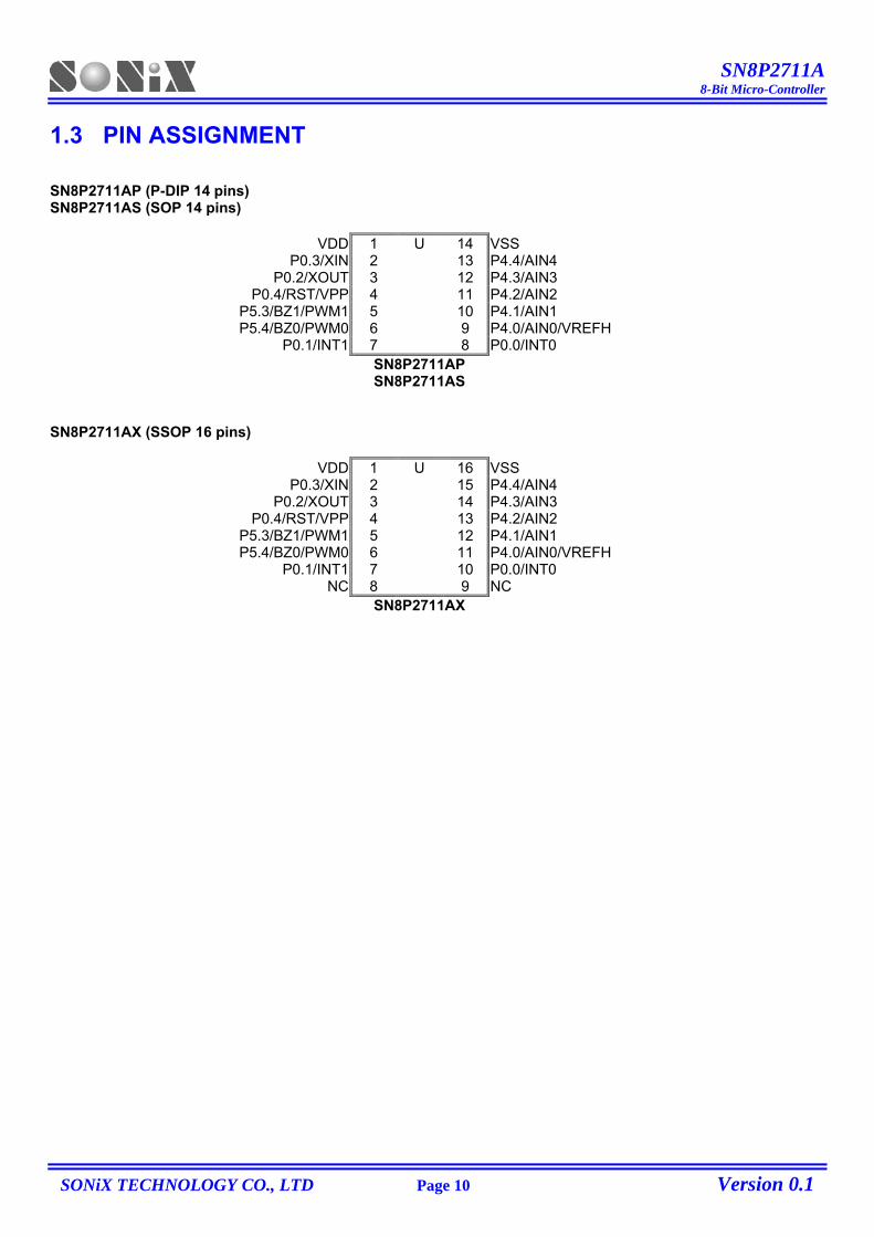
1.3 PIN ASSIGNMENT SN8P2711AP (P-DIP 14 pins) SN8P2711AS (SOP 14 pins)
VDD 1 U 14 VSS P0.3/XIN 2 13 P4.4/AIN4
P0.2/XOUT 3 12 P4.3/AIN3 P0.4/RST/VPP 4 11 P4.2/AIN2
P5.3/BZ1/PWM1 5 10 P4.1/AIN1 P5.4/BZ0/PWM0 6 9 P4.0/AIN0/VREFH
P0.1/INT1 7 8 P0.0/INT0 SN8P2711AP SN8P2711AS SN8P2711AX (SSOP 16 pins)
VDD 1 U 16 VSS P0.3/XIN 2 15 P4.4/AIN4
P0.2/XOUT 3 14 P4.3/AIN3 P0.4/RST/VPP 4 13 P4.2/AIN2
P5.3/BZ1/PWM1 5 12 P4.1/AIN1 P5.4/BZ0/PWM0 6 11 P4.0/AIN0/VREFH
P0.1/INT1 7 10 P0.0/INT0 NC 8 9 NC
SN8P2711AX
SN8P2711A 8-Bit Micro-Controller
SONiX TECHNOLOGY CO., LTD Page 11 Version 0.1
1.4 PIN DESCRIPTIONS
PIN NAME TYPE DESCRIPTION VDD, VSS P Power supply input pins for digital circuit.
P0.4/RST/VPP I, P
P0.4: Input only pin (Schmitt trigger) if disable external reset function. P0.4 without build-in pull-up resister. P0.4 is input only pin without pull-up resistor under P0.4 mode. Add the 100 ohm external resistor on P0.4, when it is set to be input pin. Built-in wakeup function. RST: System reset input pin. Schmitt trigger structure, low active, normal stay to “high”. VPP: OTP programming pin.
P0.3/XIN I/O
Port 0.3 bi-direction pin. Schmitt trigger structure as input mode. Built-in pull-up resisters. Built-in wakeup function. Oscillator input pin while external oscillator enable (crystal and RC).
P0.2/XOUT I/O
Port 0.2 bi-direction pin. Schmitt trigger structure as input mode. Built-in pull-up resisters. Built-in wakeup function. XOUT: Oscillator output pin while external crystal enable.
P0.0/INT0 I/O
Port 0.0 bi-direction pin. Schmitt trigger structure as input mode. Built-in pull-up resisters. Built-in wakeup function. INT0 trigger pin (Schmitt trigger). TC0 event counter clock input pin.
P0.1/INT1 I/O
Port 0.1 bi-direction pin. Schmitt trigger structure as input mode. Built-in pull-up resisters. Built-in wakeup function. INT1 trigger pin (Schmitt trigger). TC1 event counter clock input pin.
P4.0/AIN0/VREFH I/O
Port 4.0 bi-direction pin. No Schmitt trigger structure. Built-in pull-up resisters. AIN0: ADC channel-0 input. VREFH: ADC external high reference voltage input.
P4.[4:1]/AIN[4:1] I/O Port 4 [4:1] bi-direction pins. No Schmitt trigger structure. Built-in pull-up resisters. AIN[4:1]: ADC channel-1~4 input.
P5.3/BZ1/PWM1 I/O Port 5.3 bi-direction pin. Schmitt trigger structure as input mode. Built-in pull-up resisters. TC1 ÷ 2 signal output pin for buzzer or PWM1 output pin.
P5.4/BZ0/PWM0 I/O Port 5.4 bi-direction pin. Schmitt trigger structure as input mode. Built-in pull-up resisters. TC0 ÷ 2 signal output pin for buzzer or PWM0 output pin.
SN8P2711A 8-Bit Micro-Controller
SONiX TECHNOLOGY CO., LTD Page 12 Version 0.1
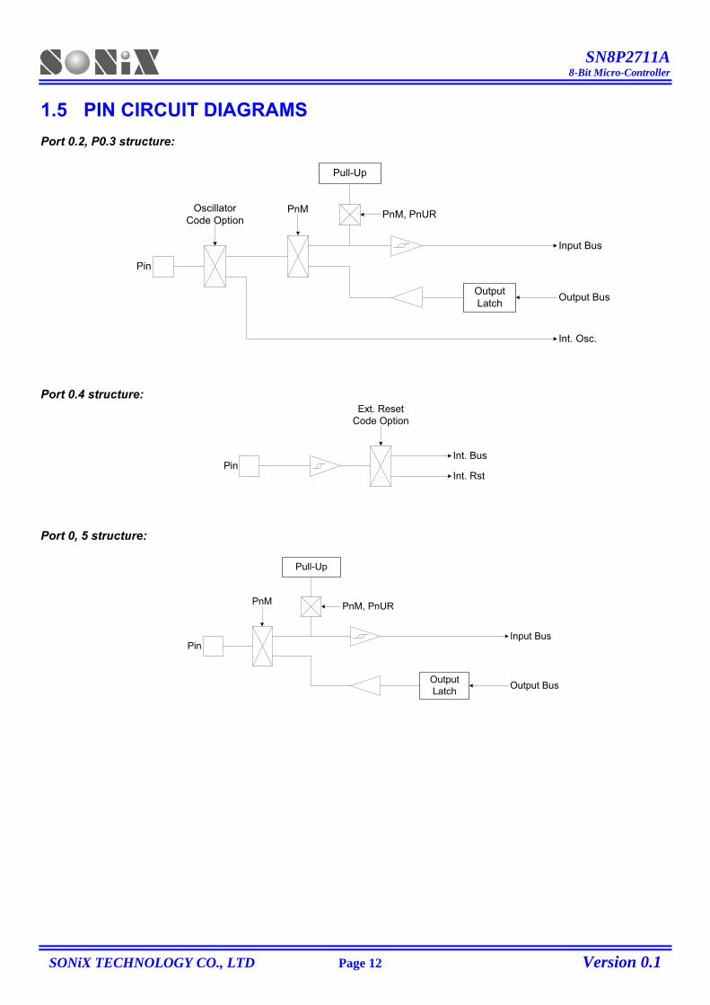
1.5 PIN CIRCUIT DIAGRAMS
Port 0.2, P0.3 structure:
OscillatorCode Option
Int. Osc.
Pull-Up
Pin
OutputLatch
PnM, PnUR
Input Bus
PnM
Output Bus
Port 0.4 structure:
Pin
Ext. ResetCode Option
Int. Bus
Int. Rst
Port 0, 5 structure:
Pull-Up
Pin
OutputLatch
PnM, PnUR
Input Bus
PnM
Output Bus
SN8P2711A 8-Bit Micro-Controller
SONiX TECHNOLOGY CO., LTD Page 13 Version 0.1
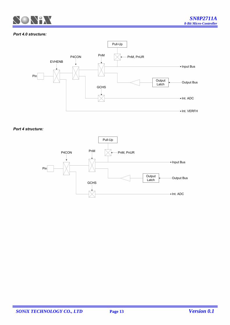
Port 4.0 structure:
Int. VERFH
Pin
EVHENB
GCHS
Int. ADC
P4CON
Pull-Up
OutputLatch
PnM, PnUR
Input Bus
PnM
Output Bus
Port 4 structure:
GCHS
Int. ADC
P4CON
Pull-Up
OutputLatch
PnM, PnUR
Input Bus
PnM
Output Bus
Pin
SN8P2711A 8-Bit Micro-Controller
SONiX TECHNOLOGY CO., LTD Page 14 Version 0.1
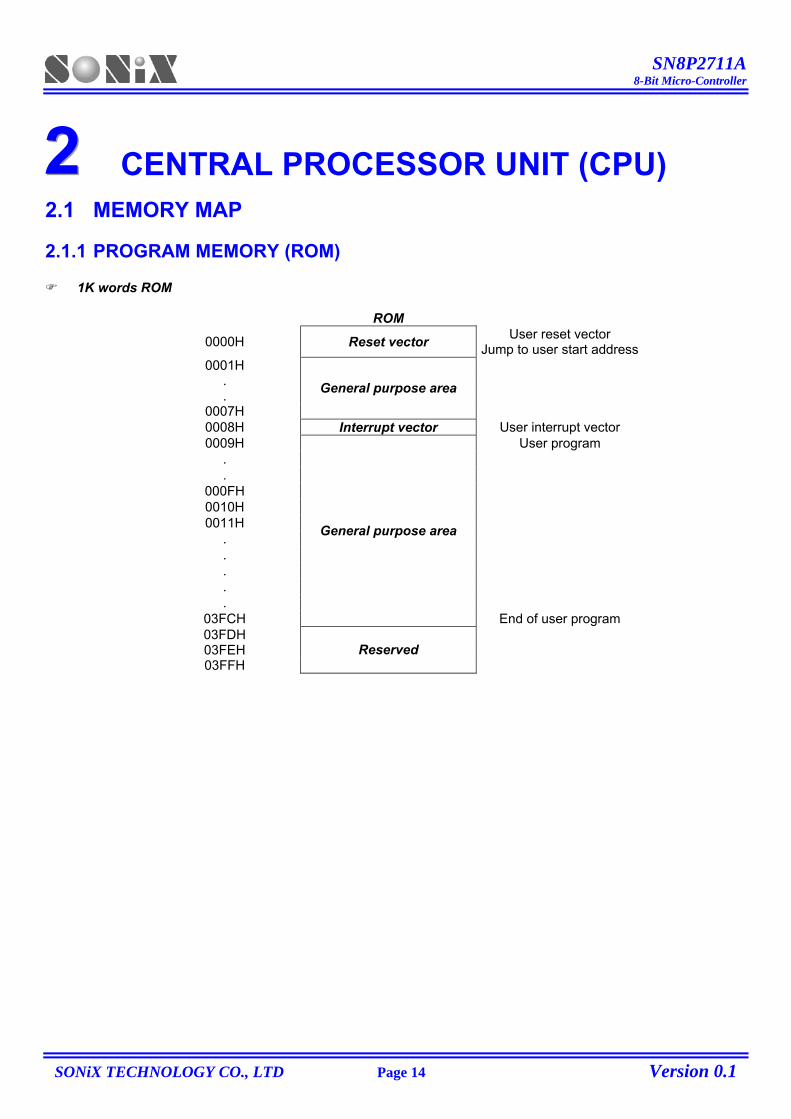
222 CENTRAL PROCESSOR UNIT (CPU)
2.1 MEMORY MAP 2.1.1 PROGRAM MEMORY (ROM)
1K words ROM
ROM
0000H Reset vector User reset vector Jump to user start address
0001H . .
0007H
General purpose area
0008H Interrupt vector User interrupt vector 0009H User program
.
. 000FH 0010H 0011H
.
.
.
.
. 03FCH
General purpose area
End of user program 03FDH 03FEH 03FFH
Reserved
SN8P2711A 8-Bit Micro-Controller
SONiX TECHNOLOGY CO., LTD Page 15 Version 0.1
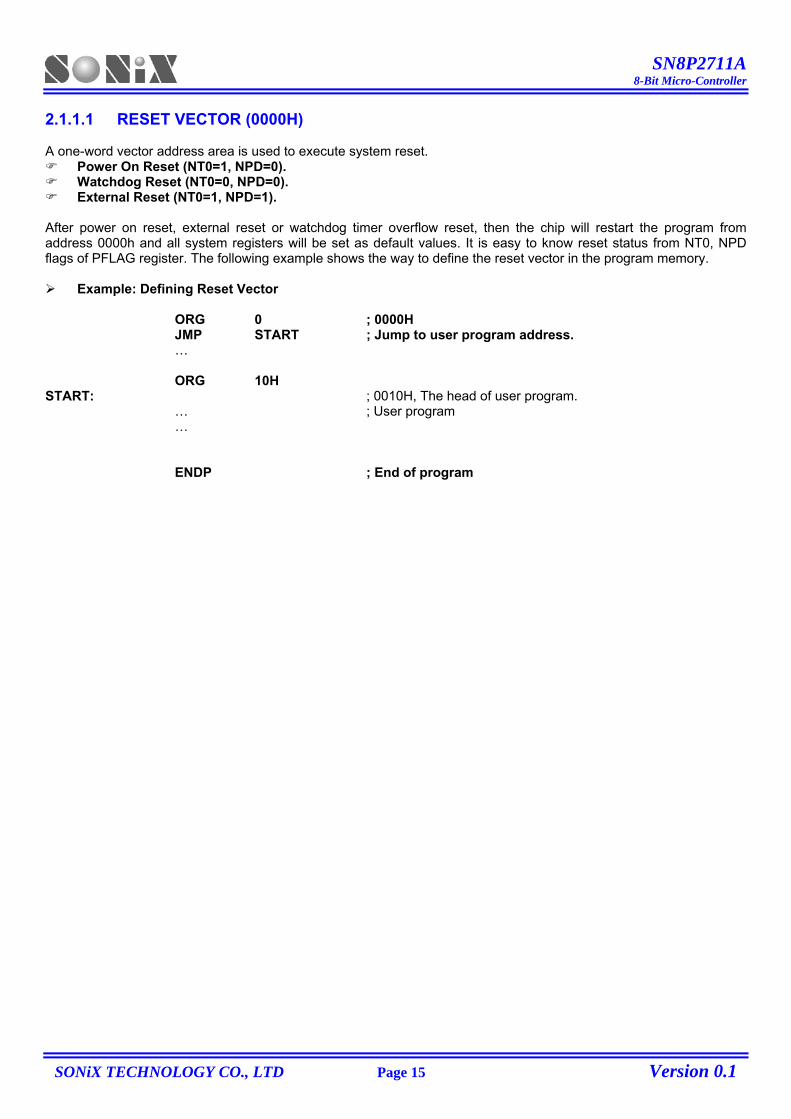
2.1.1.1 RESET VECTOR (0000H) A one-word vector address area is used to execute system reset.
Power On Reset (NT0=1, NPD=0). Watchdog Reset (NT0=0, NPD=0). External Reset (NT0=1, NPD=1).
After power on reset, external reset or watchdog timer overflow reset, then the chip will restart the program from address 0000h and all system registers will be set as default values. It is easy to know reset status from NT0, NPD flags of PFLAG register. The following example shows the way to define the reset vector in the program memory.
Example: Defining Reset Vector ORG 0 ; 0000H JMP START ; Jump to user program address. … ORG 10H START: ; 0010H, The head of user program. … ; User program … ENDP ; End of program
SN8P2711A 8-Bit Micro-Controller
SONiX TECHNOLOGY CO., LTD Page 16 Version 0.1
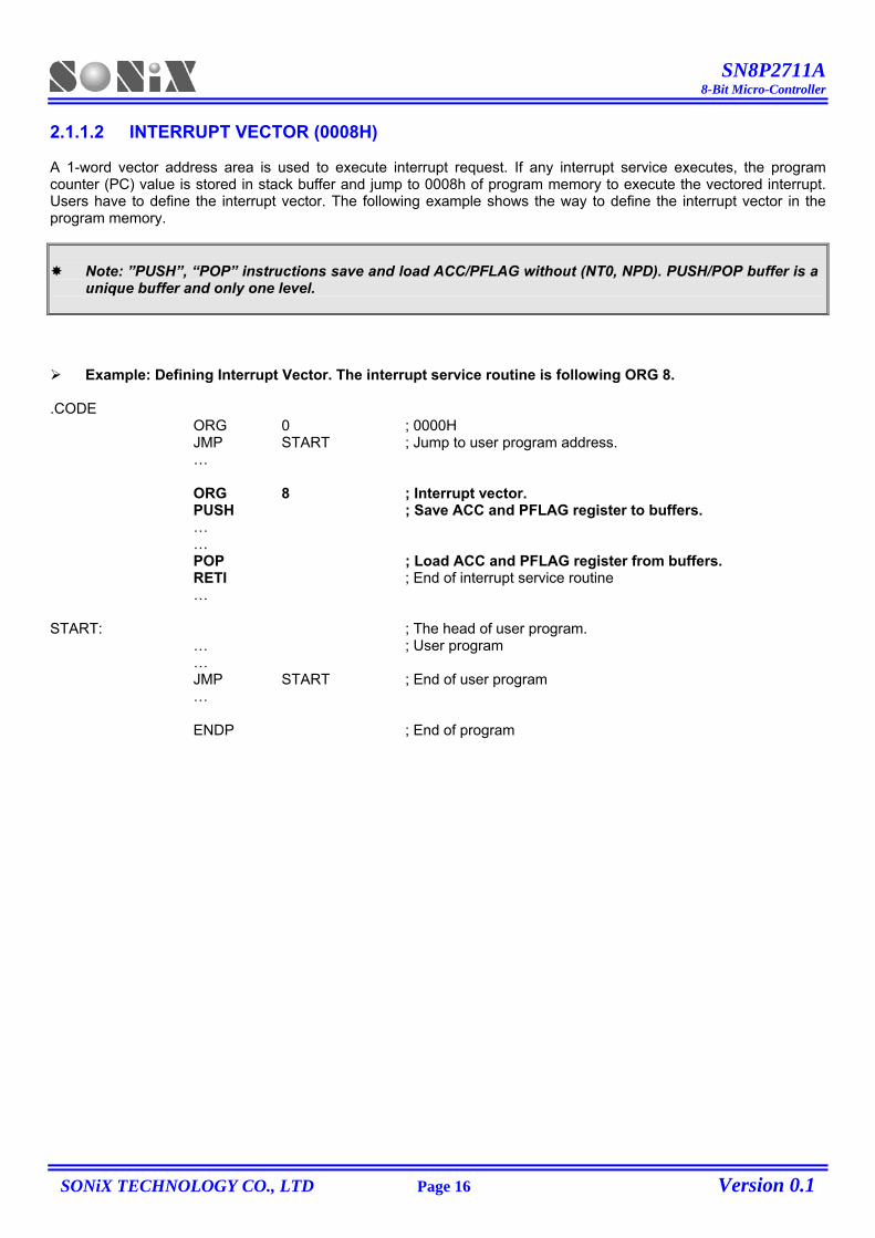
2.1.1.2 INTERRUPT VECTOR (0008H) A 1-word vector address area is used to execute interrupt request. If any interrupt service executes, the program counter (PC) value is stored in stack buffer and jump to 0008h of program memory to execute the vectored interrupt. Users have to define the interrupt vector. The following example shows the way to define the interrupt vector in the program memory.
Note: ”PUSH”, “POP” instructions save and load ACC/PFLAG without (NT0, NPD). PUSH/POP buffer is a unique buffer and only one level.
Example: Defining Interrupt Vector. The interrupt service routine is following ORG 8. .CODE ORG 0 ; 0000H JMP START ; Jump to user program address. … ORG 8 ; Interrupt vector. PUSH ; Save ACC and PFLAG register to buffers. … … POP ; Load ACC and PFLAG register from buffers. RETI ; End of interrupt service routine … START: ; The head of user program. … ; User program … JMP START ; End of user program … ENDP ; End of program
SN8P2711A 8-Bit Micro-Controller
SONiX TECHNOLOGY CO., LTD Page 17 Version 0.1
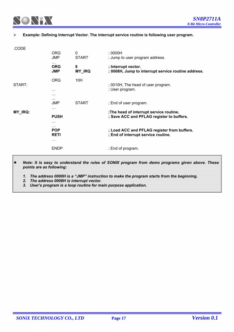
Example: Defining Interrupt Vector. The interrupt service routine is following user program.
.CODE ORG 0 ; 0000H JMP START ; Jump to user program address. … ORG 8 ; Interrupt vector. JMP MY_IRQ ; 0008H, Jump to interrupt service routine address. ORG 10H START: ; 0010H, The head of user program. … ; User program. … … JMP START ; End of user program. … MY_IRQ: ;The head of interrupt service routine. PUSH ; Save ACC and PFLAG register to buffers. … … POP ; Load ACC and PFLAG register from buffers. RETI ; End of interrupt service routine. … ENDP ; End of program.
Note: It is easy to understand the rules of SONIX program from demo programs given above. These points are as following:
1. The address 0000H is a “JMP” instruction to make the program starts from the beginning. 2. The address 0008H is interrupt vector. 3. User’s program is a loop routine for main purpose application.
SN8P2711A 8-Bit Micro-Controller
SONiX TECHNOLOGY CO., LTD Page 18 Version 0.1
2.1.1.3 LOOK-UP TABLE DESCRIPTION In the ROM’s data lookup function, Y register is pointed to middle byte address (bit 8~bit 15) and Z register is pointed to low byte address (bit 0~bit 7) of ROM. After MOVC instruction executed, the low-byte data will be stored in ACC and high-byte data stored in R register.
Example: To look up the ROM data located “TABLE1”. B0MOV Y, #TABLE1$M ; To set lookup table1’s middle address B0MOV Z, #TABLE1$L ; To set lookup table1’s low address. MOVC ; To lookup data, R = 00H, ACC = 35H ; Increment the index address for next address. INCMS Z ; Z+1 JMP @F ; Z is not overflow. INCMS Y ; Z overflow (FFH 00), Y=Y+1 NOP ; ; @@: MOVC ; To lookup data, R = 51H, ACC = 05H. … ; TABLE1: DW 0035H ; To define a word (16 bits) data. DW 5105H DW 2012H …
Note: The Y register will not increase automatically when Z register crosses boundary from 0xFF to 0x00. Therefore, user must take care such situation to avoid look-up table errors. If Z register overflows, Y register must be added one. The following INC_YZ macro shows a simple method to process Y and Z registers automatically.
Example: INC_YZ macro. INC_YZ MACRO INCMS Z ; Z+1 JMP @F ; Not overflow INCMS Y ; Y+1 NOP ; Not overflow @@: ENDM
SN8P2711A 8-Bit Micro-Controller
SONiX TECHNOLOGY CO., LTD Page 19 Version 0.1
Example: Modify above example by “INC_YZ” macro.
B0MOV Y, #TABLE1$M ; To set lookup table1’s middle address B0MOV Z, #TABLE1$L ; To set lookup table1’s low address. MOVC ; To lookup data, R = 00H, ACC = 35H INC_YZ ; Increment the index address for next address. ; @@: MOVC ; To lookup data, R = 51H, ACC = 05H. … ; TABLE1: DW 0035H ; To define a word (16 bits) data. DW 5105H DW 2012H … The other example of look-up table is to add Y or Z index register by accumulator. Please be careful if “carry” happen.
Example: Increase Y and Z register by B0ADD/ADD instruction.
B0MOV Y, #TABLE1$M ; To set lookup table’s middle address. B0MOV Z, #TABLE1$L ; To set lookup table’s low address. B0MOV A, BUF ; Z = Z + BUF. B0ADD Z, A B0BTS1 FC ; Check the carry flag. JMP GETDATA ; FC = 0 INCMS Y ; FC = 1. Y+1. NOP GETDATA: ; MOVC ; To lookup data. If BUF = 0, data is 0x0035 ; If BUF = 1, data is 0x5105 ; If BUF = 2, data is 0x2012 … TABLE1: DW 0035H ; To define a word (16 bits) data. DW 5105H DW 2012H …
SN8P2711A 8-Bit Micro-Controller
SONiX TECHNOLOGY CO., LTD Page 20 Version 0.1
2.1.1.4 JUMP TABLE DESCRIPTION The jump table operation is one of multi-address jumping function. Add low-byte program counter (PCL) and ACC value to get one new PCL. If PCL is overflow after PCL+ACC, PCH adds one automatically. The new program counter (PC) points to a series jump instructions as a listing table. It is easy to make a multi-jump program depends on the value of the accumulator (A).
Note: PCH only support PC up counting result and doesn’t support PC down counting. When PCL is carry after PCL+ACC, PCH adds one automatically. If PCL borrow after PCL–ACC, PCH keeps value and not change.
Example: Jump table.
ORG 0X0100 ; The jump table is from the head of the ROM boundary B0ADD PCL, A ; PCL = PCL + ACC, PCH + 1 when PCL overflow occurs. JMP A0POINT ; ACC = 0, jump to A0POINT JMP A1POINT ; ACC = 1, jump to A1POINT JMP A2POINT ; ACC = 2, jump to A2POINT JMP A3POINT ; ACC = 3, jump to A3POINT SONIX provides a macro for safe jump table function. This macro will check the ROM boundary and move the jump table to the right position automatically. The side effect of this macro maybe wastes some ROM size.
Example: If “jump table” crosses over ROM boundary will cause errors. @JMP_A MACRO VAL IF (($+1) !& 0XFF00) !!= (($+(VAL)) !& 0XFF00) JMP ($ | 0XFF) ORG ($ | 0XFF) ENDIF ADD PCL, A ENDM
Note: “VAL” is the number of the jump table listing number.
SN8P2711A 8-Bit Micro-Controller
SONiX TECHNOLOGY CO., LTD Page 21 Version 0.1
Example: “@JMP_A” application in SONIX macro file called “MACRO3.H”.
B0MOV A, BUF0 ; “BUF0” is from 0 to 4. @JMP_A 5 ; The number of the jump table listing is five. JMP A0POINT ; ACC = 0, jump to A0POINT JMP A1POINT ; ACC = 1, jump to A1POINT JMP A2POINT ; ACC = 2, jump to A2POINT JMP A3POINT ; ACC = 3, jump to A3POINT JMP A4POINT ; ACC = 4, jump to A4POINT If the jump table position is across a ROM boundary (0x00FF~0x0100), the “@JMP_A” macro will adjust the jump table routine begin from next RAM boundary (0x0100).
Example: “@JMP_A” operation.
; Before compiling program. ROM address B0MOV A, BUF0 ; “BUF0” is from 0 to 4. @JMP_A 5 ; The number of the jump table listing is five. 0X00FD JMP A0POINT ; ACC = 0, jump to A0POINT 0X00FE JMP A1POINT ; ACC = 1, jump to A1POINT 0X00FF JMP A2POINT ; ACC = 2, jump to A2POINT 0X0100 JMP A3POINT ; ACC = 3, jump to A3POINT 0X0101 JMP A4POINT ; ACC = 4, jump to A4POINT ; After compiling program. ROM address B0MOV A, BUF0 ; “BUF0” is from 0 to 4. @JMP_A 5 ; The number of the jump table listing is five. 0X0100 JMP A0POINT ; ACC = 0, jump to A0POINT 0X0101 JMP A1POINT ; ACC = 1, jump to A1POINT 0X0102 JMP A2POINT ; ACC = 2, jump to A2POINT 0X0103 JMP A3POINT ; ACC = 3, jump to A3POINT 0X0104 JMP A4POINT ; ACC = 4, jump to A4POINT
SN8P2711A 8-Bit Micro-Controller
SONiX TECHNOLOGY CO., LTD Page 22 Version 0.1
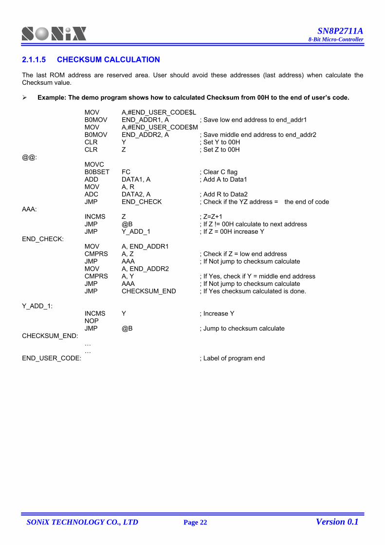
2.1.1.5 CHECKSUM CALCULATION The last ROM address are reserved area. User should avoid these addresses (last address) when calculate the Checksum value.
Example: The demo program shows how to calculated Checksum from 00H to the end of user’s code. MOV A,#END_USER_CODE$L B0MOV END_ADDR1, A ; Save low end address to end_addr1 MOV A,#END_USER_CODE$M B0MOV END_ADDR2, A ; Save middle end address to end_addr2 CLR Y ; Set Y to 00H CLR Z ; Set Z to 00H @@: MOVC B0BSET FC ; Clear C flag ADD DATA1, A ; Add A to Data1 MOV A, R ADC DATA2, A ; Add R to Data2 JMP END_CHECK ; Check if the YZ address = the end of code AAA: INCMS Z ; Z=Z+1 JMP @B ; If Z != 00H calculate to next address JMP Y_ADD_1 ; If Z = 00H increase Y END_CHECK: MOV A, END_ADDR1 CMPRS A, Z ; Check if Z = low end address JMP AAA ; If Not jump to checksum calculate MOV A, END_ADDR2 CMPRS A, Y ; If Yes, check if Y = middle end address JMP AAA ; If Not jump to checksum calculate JMP CHECKSUM_END ; If Yes checksum calculated is done. Y_ADD_1: INCMS Y ; Increase Y NOP JMP @B ; Jump to checksum calculate CHECKSUM_END: … … END_USER_CODE: ; Label of program end
SN8P2711A 8-Bit Micro-Controller
SONiX TECHNOLOGY CO., LTD Page 23 Version 0.1
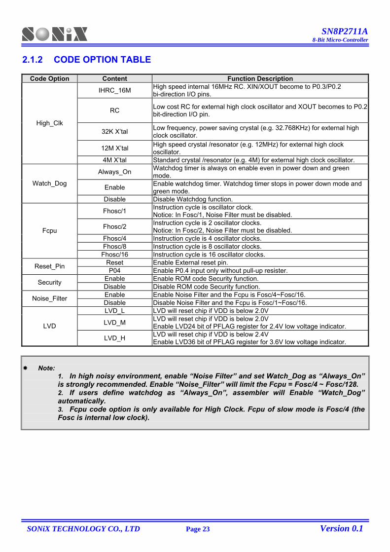
2.1.2 CODE OPTION TABLE
Code Option Content Function Description
IHRC_16M High speed internal 16MHz RC. XIN/XOUT become to P0.3/P0.2 bi-direction I/O pins.
RC Low cost RC for external high clock oscillator and XOUT becomes to P0.2 bit-direction I/O pin.
32K X’tal Low frequency, power saving crystal (e.g. 32.768KHz) for external high clock oscillator.
12M X’tal High speed crystal /resonator (e.g. 12MHz) for external high clock oscillator.
High_Clk
4M X’tal Standard crystal /resonator (e.g. 4M) for external high clock oscillator.
Always_On Watchdog timer is always on enable even in power down and green mode.
Enable Enable watchdog timer. Watchdog timer stops in power down mode and green mode.
Watch_Dog
Disable Disable Watchdog function.
Fhosc/1 Instruction cycle is oscillator clock. Notice: In Fosc/1, Noise Filter must be disabled.
Fhosc/2 Instruction cycle is 2 oscillator clocks. Notice: In Fosc/2, Noise Filter must be disabled.
Fhosc/4 Instruction cycle is 4 oscillator clocks. Fhosc/8 Instruction cycle is 8 oscillator clocks.
Fcpu
Fhosc/16 Instruction cycle is 16 oscillator clocks. Reset Enable External reset pin. Reset_Pin P04 Enable P0.4 input only without pull-up resister. Enable Enable ROM code Security function. Security Disable Disable ROM code Security function. Enable Enable Noise Filter and the Fcpu is Fosc/4~Fosc/16. Noise_Filter Disable Disable Noise Filter and the Fcpu is Fosc/1~Fosc/16. LVD_L LVD will reset chip if VDD is below 2.0V
LVD_M LVD will reset chip if VDD is below 2.0V Enable LVD24 bit of PFLAG register for 2.4V low voltage indicator. LVD
LVD_H LVD will reset chip if VDD is below 2.4V Enable LVD36 bit of PFLAG register for 3.6V low voltage indicator.
Note: 1. In high noisy environment, enable “Noise Filter” and set Watch_Dog as “Always_On” is strongly recommended. Enable “Noise_Filter” will limit the Fcpu = Fosc/4 ~ Fosc/128. 2. If users define watchdog as “Always_On”, assembler will Enable “Watch_Dog” automatically. 3. Fcpu code option is only available for High Clock. Fcpu of slow mode is Fosc/4 (the Fosc is internal low clock).
SN8P2711A 8-Bit Micro-Controller
SONiX TECHNOLOGY CO., LTD Page 24 Version 0.1
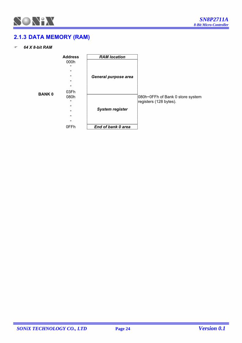
2.1.3 DATA MEMORY (RAM)
64 X 8-bit RAM
Address RAM location 000h
“ “
“ “ “
03Fh
General purpose area
080h
“ 080h~0FFh of Bank 0 store system registers (128 bytes).
“ “ “ “
System register
BANK 0
0FFh End of bank 0 area
SN8P2711A 8-Bit Micro-Controller
SONiX TECHNOLOGY CO., LTD Page 25 Version 0.1
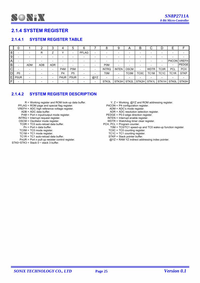
2.1.4 SYSTEM REGISTER 2.1.4.1 SYSTEM REGISTER TABLE 0 1 2 3 4 5 6 7 8 9 A B C D E F 8 - - R Z Y - PFLAG - - - - - - - - - 9 - - - - - - - - - - - - - - - - A - - - - - - - - - - - - - - P4CON VREFHB - ADM ADB ADR - - - - P0M - - - - - - PEDGE
C - - - - P4M P5M - - INTRQ INTEN OSCM - WDTR TC0R PCL PCHD P0 - - - P4 P5 - - T0M - TC0M TC0C TC1M TC1C TC1R STKPE P0UR - - - P4UR P5UR - @YZ - - - - - - - - F - - - - - - - - STK3L STK3H STK2L STK2H STK1L STK1H STK0L STK0H
2.1.4.2 SYSTEM REGISTER DESCRIPTION
R = Working register and ROM look-up data buffer. Y, Z = Working, @YZ and ROM addressing register. PFLAG = ROM page and special flag register. P4CON = P4 configuration register. VREFH = ADC high reference voltage register. ADM = ADC’s mode register.
ADB = ADC data buffer. ADR = ADC resolution selection register. PnM = Port n input/output mode register. PEDGE = P0.0 edge direction register.
INTRQ = Interrupt request register. INTEN = Interrupt enable register. OSCM = Oscillator mode register. WDTR = Watchdog timer clear register. TC0R = TC0 auto-reload data buffer. PCH, PCL = Program counter.
Pn = Port n data buffer. T0M = TC0/TC1 speed-up and TC0 wake-up function register. TC0M = TC0 mode register. TC0C = TC0 counting register. TC1M = TC1 mode register. TC1C = TC1 counting register. TC1R = TC1 auto-reload data buffer. STKP = Stack pointer buffer. PnUR = Port n pull-up resister control register. @YZ = RAM YZ indirect addressing index pointer.
STK0~STK3 = Stack 0 ~ stack 3 buffer.
SN8P2711A 8-Bit Micro-Controller
SONiX TECHNOLOGY CO., LTD Page 26 Version 0.1
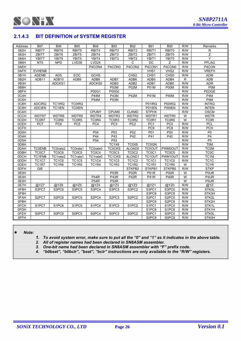
2.1.4.3 BIT DEFINITION of SYSTEM REGISTER
Address Bit7 Bit6 Bit5 Bit4 Bit3 Bit2 Bit1 Bit0 R/W Remarks 082H RBIT7 RBIT6 RBIT5 RBIT4 RBIT3 RBIT2 RBIT1 RBIT0 R/W R 083H ZBIT7 ZBIT6 ZBIT5 ZBIT4 ZBIT3 ZBIT2 ZBIT1 ZBIT0 R/W Z 084H YBIT7 YBIT6 YBIT5 YBIT4 YBIT3 YBIT2 YBIT1 YBIT0 R/W Y 086H NT0 NPD LVD36 LVD24 C DC Z R/W PFLAG 0AEH P4CON4 P4CON3 P4CON2 P4CON1 P4CON0 R/W P4CON 0AFH EVHENB VHS1 VHS2 R/W VREFH 0B1H ADENB ADS EOC GCHS CHS2 CHS1 CHS0 R/W ADM 0B2H ADB11 ADB10 ADB9 ADB8 ADB7 ADB6 ADB5 ADB4 R ADB 0B3H ADCKS1 ADCKS0 ADB3 ADB2 ADB1 ADB0 R/W ADR 0B8H P03M P02M P01M P00M R/W P0M 0BFH P00G1 P00G0 R/W PEDGE 0C4H P44M P43M P42M P41M P40M R/W P4M 0C5H P54M P53M R/W P5M 0C8H ADCIRQ TC1IRQ TC0IRQ P01IRQ P00IRQ R/W INTRQ 0C9H ADCIEN TC1IEN TC0IEN P01IEN P00IEN R/W INTEN 0CAH CPUM1 CPUM0 CLKMD STPHX R/W OSCM 0CCH WDTR7 WDTR6 WDTR5 WDTR4 WDTR3 WDTR2 WDTR1 WDTR0 W WDTR 0CDH TC0R7 TC0R6 TC0R5 TC0R4 TC0R3 TC0R2 TC0R1 TC0R0 W TC0R 0CEH PC7 PC6 PC5 PC4 PC3 PC2 PC1 PC0 R/W PCL 0CFH PC9 PC8 R/W PCH 0D0H P04 P03 P02 P01 P00 R/W P0 0D4H P44 P43 P42 P41 P40 R/W P4 0D5H P54 P53 R/W P5 0D8H TC1X8 TC0X8 TC0GN R/W T0M 0DAH TC0ENB TC0rate2 TC0rate1 TC0rate0 TC0CKS ALOAD0 TC0OUT PWM0OUT R/W TC0M 0DBH TC0C7 TC0C6 TC0C5 TC0C4 TC0C3 TC0C2 TC0C1 TC0C0 R/W TC0C 0DCH TC1ENB TC1rate2 TC1rate1 TC1rate0 TC1CKS ALOAD1 TC1OUT PWM1OUT R/W TC1M 0DDH TC1C7 TC1C6 TC1C5 TC1C4 TC1C3 TC1C2 TC1C1 TC1C0 R/W TC1C 0DEH TC1R7 TC1R6 TC1R5 TC1R4 TC1R3 TC1R2 TC1R1 TC1R0 W TC1R 0DFH GIE STKPB2 STKPB1 STKPB0 R/W STKP 0E0H P03R P02R P01R P00R W P0UR 0E4H P44R P43R P42R P41R P40R W P4UR 0E5H P54R P53R W P5UR 0E7H @YZ7 @YZ6 @YZ5 @YZ4 @YZ3 @YZ2 @YZ1 @YZ0 R/W @YZ 0F8H S3PC7 S3PC6 S3PC5 S3PC4 S3PC3 S3PC2 S3PC1 S3PC0 R/W STK3L 0F9H S3PC9 S3PC8 R/W STK3H 0FAH S2PC7 S2PC6 S2PC5 S2PC4 S2PC3 S2PC2 S2PC1 S2PC0 R/W STK2L 0FBH S2PC9 S2PC8 R/W STK2H 0FCH S1PC7 S1PC6 S1PC5 S1PC4 S1PC3 S1PC2 S1PC1 S1PC0 R/W STK1L 0FDH S1PC9 S1PC8 R/W STK1H 0FEH S0PC7 S0PC6 S0PC5 S0PC4 S0PC3 S0PC2 S0PC1 S0PC0 R/W STK0L 0FFH S0PC9 S0PC8 R/W STK0H
Note: 1. To avoid system error, make sure to put all the “0” and “1” as it indicates in the above table. 2. All of register names had been declared in SN8ASM assembler. 3. One-bit name had been declared in SN8ASM assembler with “F” prefix code. 4. “b0bset”, “b0bclr”, ”bset”, ”bclr” instructions are only available to the “R/W” registers.
SN8P2711A 8-Bit Micro-Controller
SONiX TECHNOLOGY CO., LTD Page 27 Version 0.1
2.1.4.4 ACCUMULATOR The ACC is an 8-bit data register responsible for transferring or manipulating data between ALU and data memory. If the result of operating is zero (Z) or there is carry (C or DC) occurrence, then these flags will be set to PFLAG register. ACC is not in data memory (RAM), so ACC can’t be access by “B0MOV” instruction during the instant addressing mode.
Example: Read and write ACC value. ; Read ACC data and store in BUF data memory. MOV BUF, A ; Write a immediate data into ACC. MOV A, #0FH ; Write ACC data from BUF data memory. MOV A, BUF ; or B0MOV A, BUF The system doesn’t store ACC and PFLAG value when interrupt executed. ACC and PFLAG data must be saved to other data memories. “PUSH”, “POP” save and load ACC, PFLAG data into buffers.
Example: Protect ACC and working registers. INT_SERVICE: PUSH ; Save ACC and PFLAG to buffers. … . … POP ; Load ACC and PFLAG from buffers. RETI ; Exit interrupt service vector
SN8P2711A 8-Bit Micro-Controller
SONiX TECHNOLOGY CO., LTD Page 28 Version 0.1
2.1.4.5 PROGRAM FLAG The PFLAG register contains the arithmetic status of ALU operation, system reset status and LVD detecting status. NT0, NPD bits indicate system reset status including power on reset, LVD reset, reset by external pin active and watchdog reset. C, DC, Z bits indicate the result status of ALU operation. LVD24, LVD36 bits indicate LVD detecting power voltage status.
086H Bit 7 Bit 6 Bit 5 Bit 4 Bit 3 Bit 2 Bit 1 Bit 0 PFLAG NT0 NPD LVD36 LVD24 - C DC Z
Read/Write R/W R/W R R - R/W R/W R/W After reset - - 0 0 - 0 0 0
Bit [7:6] NT0, NPD: Reset status flag.
NT0 NPD Reset Status 0 0 Watch-dog time out 0 1 Reserved 1 0 Reset by LVD 1 1 Reset by external Reset Pin
Bit 5 LVD36: LVD 3.6V operating flag and only support LVD code option is LVD_H.
0 = Inactive (VDD > 3.6V). 1 = Active (VDD <= 3.6V).
Bit 4 LVD24: LVD 2.4V operating flag and only support LVD code option is LVD_M. 0 = Inactive (VDD > 2.4V). 1 = Active (VDD <= 2.4V).
Bit 2 C: Carry flag
1 = Addition with carry, subtraction without borrowing, rotation with shifting out logic “1”, comparison result ≥ 0.
0 = Addition without carry, subtraction with borrowing signal, rotation with shifting out logic “0”, comparison result < 0.
Bit 1 DC: Decimal carry flag
1 = Addition with carry from low nibble, subtraction without borrow from high nibble. 0 = Addition without carry from low nibble, subtraction with borrow from high nibble.
Bit 0 Z: Zero flag 1 = The result of an arithmetic/logic/branch operation is zero. 0 = The result of an arithmetic/logic/branch operation is not zero.
Note: Refer to instruction set table for detailed information of C, DC and Z flags.
SN8P2711A 8-Bit Micro-Controller
SONiX TECHNOLOGY CO., LTD Page 29 Version 0.1
2.1.4.6 PROGRAM COUNTER The program counter (PC) is a 10-bit binary counter separated into the high-byte 2 and the low-byte 8 bits. This counter is responsible for pointing a location in order to fetch an instruction for kernel circuit. Normally, the program counter is automatically incremented with each instruction during program execution. Besides, it can be replaced with specific address by executing CALL or JMP instruction. When JMP or CALL instruction is executed, the destination address will be inserted to bit 0 ~ bit 9.
Bit 15 Bit 14 Bit 13 Bit 12 Bit 11 Bit 10 Bit 9 Bit 8 Bit 7 Bit 6 Bit 5 Bit 4 Bit 3 Bit 2 Bit 1 Bit 0PC - - - - - - PC9 PC8 PC7 PC6 PC5 PC4 PC3 PC2 PC1 PC0
After reset - - - - - - 0 0 0 0 0 0 0 0 0 0
PCH PCL
ONE ADDRESS SKIPPING There are nine instructions (CMPRS, INCS, INCMS, DECS, DECMS, BTS0, BTS1, B0BTS0, B0BTS1) with one address skipping function. If the result of these instructions is true, the PC will add 2 steps to skip next instruction. If the condition of bit test instruction is true, the PC will add 2 steps to skip next instruction. B0BTS1 FC ; To skip, if Carry_flag = 1 JMP C0STEP ; Else jump to C0STEP. … … C0STEP: NOP B0MOV A, BUF0 ; Move BUF0 value to ACC. B0BTS0 FZ ; To skip, if Zero flag = 0. JMP C1STEP ; Else jump to C1STEP. … … C1STEP: NOP If the ACC is equal to the immediate data or memory, the PC will add 2 steps to skip next instruction. CMPRS A, #12H ; To skip, if ACC = 12H. JMP C0STEP ; Else jump to C0STEP. … … C0STEP: NOP
SN8P2711A 8-Bit Micro-Controller
SONiX TECHNOLOGY CO., LTD Page 30 Version 0.1
If the destination increased by 1, which results overflow of 0xFF to 0x00, the PC will add 2 steps to skip next instruction. INCS instruction: INCS BUF0 JMP C0STEP ; Jump to C0STEP if ACC is not zero. … … C0STEP: NOP INCMS instruction: INCMS BUF0 JMP C0STEP ; Jump to C0STEP if BUF0 is not zero. … … C0STEP: NOP If the destination decreased by 1, which results underflow of 0x00 to 0xFF, the PC will add 2 steps to skip next instruction. DECS instruction: DECS BUF0 JMP C0STEP ; Jump to C0STEP if ACC is not zero. … … C0STEP: NOP DECMS instruction: DECMS BUF0 JMP C0STEP ; Jump to C0STEP if BUF0 is not zero. … … C0STEP: NOP
SN8P2711A 8-Bit Micro-Controller
SONiX TECHNOLOGY CO., LTD Page 31 Version 0.1
MULTI-ADDRESS JUMPING
Users can jump around the multi-address by either JMP instruction or ADD M, A instruction (M = PCL) to activate multi-address jumping function. Program Counter supports “ADD M,A”, ”ADC M,A” and “B0ADD M,A” instructions for carry to PCH when PCL overflow automatically. For jump table or others applications, users can calculate PC value by the three instructions and don’t care PCL overflow problem.
Note: PCH only support PC up counting result and doesn’t support PC down counting. When PCL is carry after PCL+ACC, PCH adds one automatically. If PCL borrow after PCL–ACC, PCH keeps value and not change.
Example: If PC = 0323H (PCH = 03H, PCL = 23H) ; PC = 0323H MOV A, #28H B0MOV PCL, A ; Jump to address 0328H … ; PC = 0328H MOV A, #00H B0MOV PCL, A ; Jump to address 0300H …
Example: If PC = 0323H (PCH = 03H, PCL = 23H) ; PC = 0323H B0ADD PCL, A ; PCL = PCL + ACC, the PCH cannot be changed. JMP A0POINT ; If ACC = 0, jump to A0POINT JMP A1POINT ; ACC = 1, jump to A1POINT JMP A2POINT ; ACC = 2, jump to A2POINT JMP A3POINT ; ACC = 3, jump to A3POINT … …
SN8P2711A 8-Bit Micro-Controller
SONiX TECHNOLOGY CO., LTD Page 32 Version 0.1
2.1.4.7 Y, Z REGISTERS The Y and Z registers are the 8-bit buffers. There are three major functions of these registers.
can be used as general working registers can be used as RAM data pointers with @YZ register can be used as ROM data pointer with the MOVC instruction for look-up table
084H Bit 7 Bit 6 Bit 5 Bit 4 Bit 3 Bit 2 Bit 1 Bit 0 Y YBIT7 YBIT6 YBIT5 YBIT4 YBIT3 YBIT2 YBIT1 YBIT0
Read/Write R/W R/W R/W R/W R/W R/W R/W R/W After reset - - - - - - - -
083H Bit 7 Bit 6 Bit 5 Bit 4 Bit 3 Bit 2 Bit 1 Bit 0
Z ZBIT7 ZBIT6 ZBIT5 ZBIT4 ZBIT3 ZBIT2 ZBIT1 ZBIT0 Read/Write R/W R/W R/W R/W R/W R/W R/W R/W After reset - - - - - - - -
Example: Uses Y, Z register as the data pointer to access data in the RAM address 025H of bank0. B0MOV Y, #00H ; To set RAM bank 0 for Y register B0MOV Z, #25H ; To set location 25H for Z register B0MOV A, @YZ ; To read a data into ACC Example: Uses the Y, Z register as data pointer to clear the RAM data. B0MOV Y, #0 ; Y = 0, bank 0 B0MOV Z, #07FH ; Z = 7FH, the last address of the data memory area CLR_YZ_BUF: CLR @YZ ; Clear @YZ to be zero DECMS Z ; Z – 1, if Z= 0, finish the routine JMP CLR_YZ_BUF ; Not zero CLR @YZ END_CLR: ; End of clear general purpose data memory area of bank 0 …
SN8P2711A 8-Bit Micro-Controller
SONiX TECHNOLOGY CO., LTD Page 33 Version 0.1
2.1.4.8 R REGISTERS R register is an 8-bit buffer. There are two major functions of the register.
Can be used as working register For store high-byte data of look-up table
(MOVC instruction executed, the high-byte data of specified ROM address will be stored in R register and the low-byte data will be stored in ACC).
082H Bit 7 Bit 6 Bit 5 Bit 4 Bit 3 Bit 2 Bit 1 Bit 0
R RBIT7 RBIT6 RBIT5 RBIT4 RBIT3 RBIT2 RBIT1 RBIT0 Read/Write R/W R/W R/W R/W R/W R/W R/W R/W After reset - - - - - - - -
Note: Please refer to the “LOOK-UP TABLE DESCRIPTION” about R register look-up table application.
SN8P2711A 8-Bit Micro-Controller
SONiX TECHNOLOGY CO., LTD Page 34 Version 0.1
2.2 ADDRESSING MODE 2.2.1 IMMEDIATE ADDRESSING MODE The immediate addressing mode uses an immediate data to set up the location in ACC or specific RAM.
Example: Move the immediate data 12H to ACC. MOV A, #12H ; To set an immediate data 12H into ACC.
Example: Move the immediate data 12H to R register. B0MOV R, #12H ; To set an immediate data 12H into R register.
Note: In immediate addressing mode application, the specific RAM must be 0x80~0x87 working register. 2.2.2 DIRECTLY ADDRESSING MODE The directly addressing mode moves the content of RAM location in or out of ACC.
Example: Move 0x12 RAM location data into ACC. B0MOV A, 12H ; To get a content of RAM location 0x12 of bank 0 and save in
ACC.
Example: Move ACC data into 0x12 RAM location. B0MOV 12H, A ; To get a content of ACC and save in RAM location 12H of
bank 0. 2.2.3 INDIRECTLY ADDRESSING MODE The indirectly addressing mode is to access the memory by the data pointer registers (Y/Z).
Example: Indirectly addressing mode with @YZ register. B0MOV Y, #0 ; To clear Y register to access RAM bank 0. B0MOV Z, #12H ; To set an immediate data 12H into Z register. B0MOV A, @YZ ; Use data pointer @YZ reads a data from RAM location ; 012H into ACC.
SN8P2711A 8-Bit Micro-Controller
SONiX TECHNOLOGY CO., LTD Page 35 Version 0.1
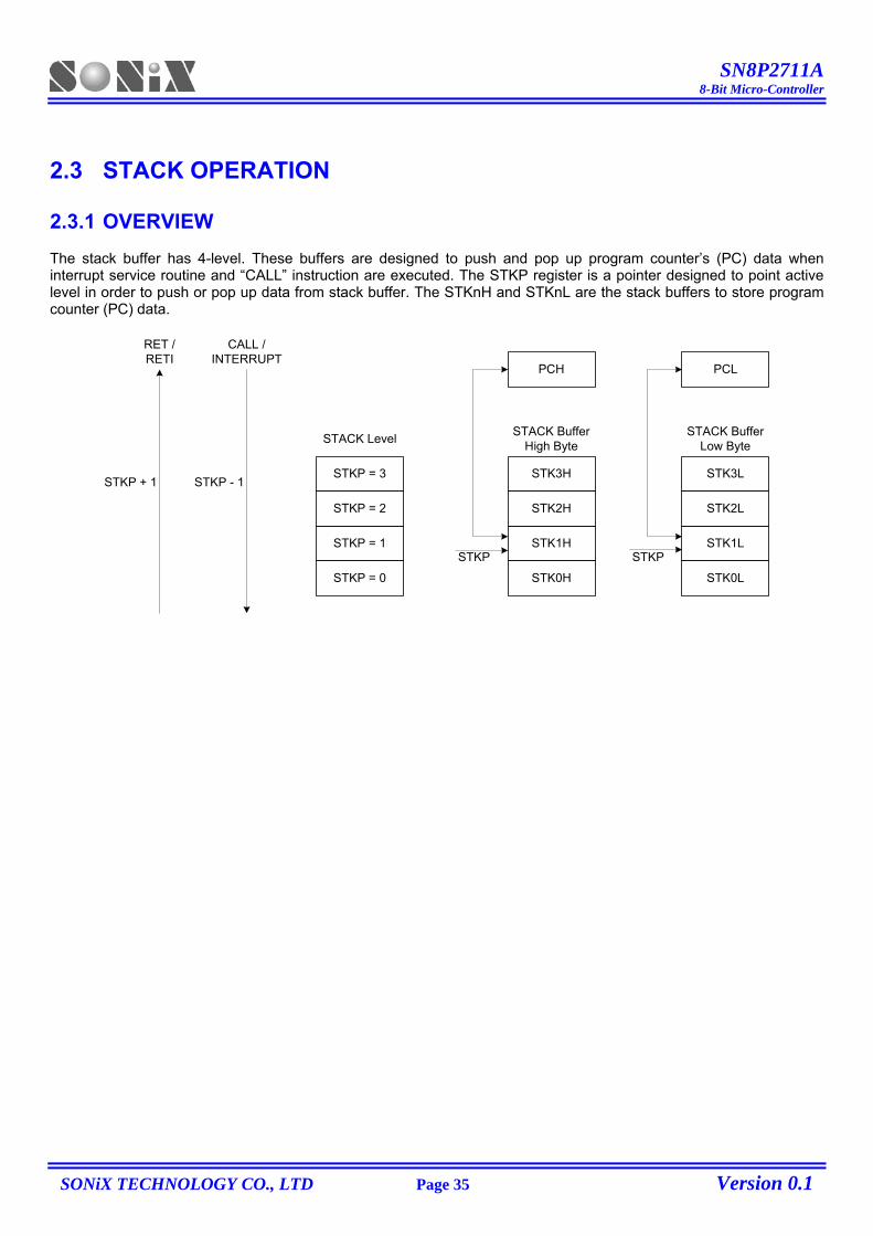
2.3 STACK OPERATION 2.3.1 OVERVIEW The stack buffer has 4-level. These buffers are designed to push and pop up program counter’s (PC) data when interrupt service routine and “CALL” instruction are executed. The STKP register is a pointer designed to point active level in order to push or pop up data from stack buffer. The STKnH and STKnL are the stack buffers to store program counter (PC) data.
RET /RETI
CALL /INTERRUPT
STKP = 3
STKP = 2
STKP = 1
STKP = 0
STACK Level
STK3H
STK2H
STK1H
STK0H
STACK BufferHigh Byte
PCH
STKP
STK3L
STK2L
STK1L
STK0L
STACK BufferLow Byte
PCL
STKP
STKP - 1STKP + 1
SN8P2711A 8-Bit Micro-Controller
SONiX TECHNOLOGY CO., LTD Page 36 Version 0.1
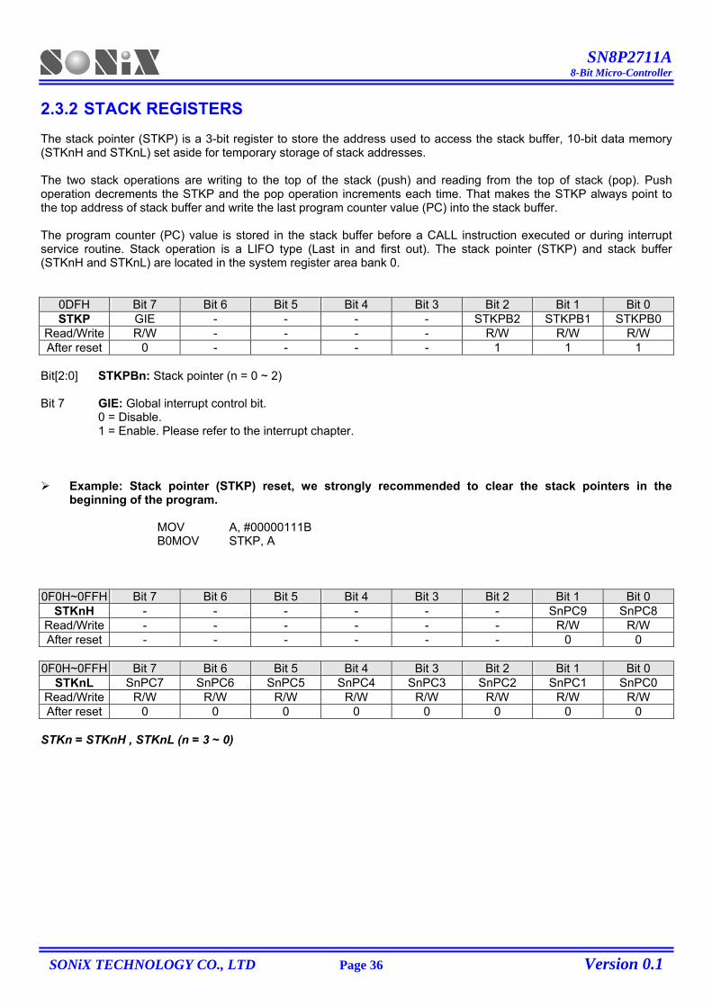
2.3.2 STACK REGISTERS The stack pointer (STKP) is a 3-bit register to store the address used to access the stack buffer, 10-bit data memory (STKnH and STKnL) set aside for temporary storage of stack addresses. The two stack operations are writing to the top of the stack (push) and reading from the top of stack (pop). Push operation decrements the STKP and the pop operation increments each time. That makes the STKP always point to the top address of stack buffer and write the last program counter value (PC) into the stack buffer. The program counter (PC) value is stored in the stack buffer before a CALL instruction executed or during interrupt service routine. Stack operation is a LIFO type (Last in and first out). The stack pointer (STKP) and stack buffer (STKnH and STKnL) are located in the system register area bank 0.
0DFH Bit 7 Bit 6 Bit 5 Bit 4 Bit 3 Bit 2 Bit 1 Bit 0 STKP GIE - - - - STKPB2 STKPB1 STKPB0
Read/Write R/W - - - - R/W R/W R/W After reset 0 - - - - 1 1 1
Bit[2:0] STKPBn: Stack pointer (n = 0 ~ 2) Bit 7 GIE: Global interrupt control bit.
0 = Disable. 1 = Enable. Please refer to the interrupt chapter.
Example: Stack pointer (STKP) reset, we strongly recommended to clear the stack pointers in the beginning of the program.
MOV A, #00000111B B0MOV STKP, A 0F0H~0FFH Bit 7 Bit 6 Bit 5 Bit 4 Bit 3 Bit 2 Bit 1 Bit 0
STKnH - - - - - - SnPC9 SnPC8 Read/Write - - - - - - R/W R/W After reset - - - - - - 0 0
0F0H~0FFH Bit 7 Bit 6 Bit 5 Bit 4 Bit 3 Bit 2 Bit 1 Bit 0
STKnL SnPC7 SnPC6 SnPC5 SnPC4 SnPC3 SnPC2 SnPC1 SnPC0 Read/Write R/W R/W R/W R/W R/W R/W R/W R/W After reset 0 0 0 0 0 0 0 0
STKn = STKnH , STKnL (n = 3 ~ 0)
SN8P2711A 8-Bit Micro-Controller
SONiX TECHNOLOGY CO., LTD Page 37 Version 0.1
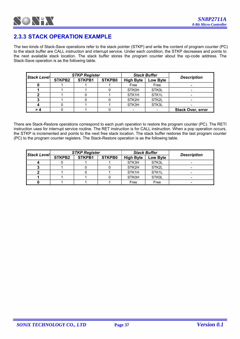
2.3.3 STACK OPERATION EXAMPLE The two kinds of Stack-Save operations refer to the stack pointer (STKP) and write the content of program counter (PC) to the stack buffer are CALL instruction and interrupt service. Under each condition, the STKP decreases and points to the next available stack location. The stack buffer stores the program counter about the op-code address. The Stack-Save operation is as the following table.
STKP Register Stack Buffer Stack Level STKPB2 STKPB1 STKPB0 High Byte Low Byte Description
0 1 1 1 Free Free - 1 1 1 0 STK0H STK0L - 2 1 0 1 STK1H STK1L - 3 1 0 0 STK2H STK2L - 4 0 1 1 STK3H STK3L -
> 4 0 1 0 - - Stack Over, error There are Stack-Restore operations correspond to each push operation to restore the program counter (PC). The RETI instruction uses for interrupt service routine. The RET instruction is for CALL instruction. When a pop operation occurs, the STKP is incremented and points to the next free stack location. The stack buffer restores the last program counter (PC) to the program counter registers. The Stack-Restore operation is as the following table.
STKP Register Stack Buffer Stack Level STKPB2 STKPB1 STKPB0 High Byte Low Byte Description
4 0 1 1 STK3H STK3L - 3 1 0 0 STK2H STK2L - 2 1 0 1 STK1H STK1L - 1 1 1 0 STK0H STK0L - 0 1 1 1 Free Free -
SN8P2711A 8-Bit Micro-Controller
SONiX TECHNOLOGY CO., LTD Page 38 Version 0.1
333 RESET
3.1 OVERVIEW The system would be reset in three conditions as following.
Power on reset Watchdog reset Brown out reset External reset (only supports external reset pin enable situation)
When any reset condition occurs, all system registers keep initial status, program stops and program counter is cleared. After reset status released, the system boots up and program starts to execute from ORG 0. The NT0, NPD flags indicate system reset status. The system can depend on NT0, NPD status and go to different paths by program.
086H Bit 7 Bit 6 Bit 5 Bit 4 Bit 3 Bit 2 Bit 1 Bit 0 PFLAG NT0 NPD LVD36 LVD24 - C DC Z
Read/Write R/W R/W R R - R/W R/W R/W After reset - - 0 0 - 0 0 0
Bit [7:6] NT0, NPD: Reset status flag.
NT0 NPD Condition Description 0 0 Watchdog reset Watchdog timer overflow. 0 1 Reserved - 1 0 Power on reset and LVD reset. Power voltage is lower than LVD detecting level.1 1 External reset External reset pin detect low level status.
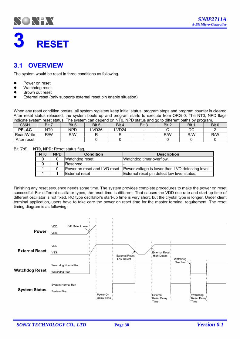
Finishing any reset sequence needs some time. The system provides complete procedures to make the power on reset successful. For different oscillator types, the reset time is different. That causes the VDD rise rate and start-up time of different oscillator is not fixed. RC type oscillator’s start-up time is very short, but the crystal type is longer. Under client terminal application, users have to take care the power on reset time for the master terminal requirement. The reset timing diagram is as following.
VDD
VSS
VDD
VSS
Watchdog Normal Run
Watchdog Stop
System Normal Run
System Stop
LVD Detect Level
External Reset Low Detect
External Reset High Detect
Watchdog Overflow
WatchdogReset DelayTime
ExternalReset DelayTime
Power OnDelay Time
Power
External Reset
Watchdog Reset
System Status
SN8P2711A 8-Bit Micro-Controller
SONiX TECHNOLOGY CO., LTD Page 39 Version 0.1
3.2 POWER ON RESET The power on reset depend no LVD operation for most power-up situations. The power supplying to system is a rising curve and needs some time to achieve the normal voltage. Power on reset sequence is as following.
Power-up: System detects the power voltage up and waits for power stable. External reset (only external reset pin enable): System checks external reset pin status. If external reset pin is
not high level, the system keeps reset status and waits external reset pin released. System initialization: All system registers is set as initial conditions and system is ready. Oscillator warm up: Oscillator operation is successfully and supply to system clock. Program executing: Power on sequence is finished and program executes from ORG 0.
3.3 WATCHDOG RESET Watchdog reset is a system protection. In normal condition, system works well and clears watchdog timer by program. Under error condition, system is in unknown situation and watchdog can’t be clear by program before watchdog timer overflow. Watchdog timer overflow occurs and the system is reset. After watchdog reset, the system restarts and returns normal mode. Watchdog reset sequence is as following.
Watchdog timer status: System checks watchdog timer overflow status. If watchdog timer overflow occurs, the system is reset.
System initialization: All system registers is set as initial conditions and system is ready. Oscillator warm up: Oscillator operation is successfully and supply to system clock. Program executing: Power on sequence is finished and program executes from ORG 0.
Watchdog timer application note is as following.
Before clearing watchdog timer, check I/O status and check RAM contents can improve system error. Don’t clear watchdog timer in interrupt vector and interrupt service routine. That can improve main routine fail. Clearing watchdog timer program is only at one part of the program. This way is the best structure to enhance the
watchdog timer function.
Note: Please refer to the “WATCHDOG TIMER” about watchdog timer detail information.
SN8P2711A 8-Bit Micro-Controller
SONiX TECHNOLOGY CO., LTD Page 40 Version 0.1
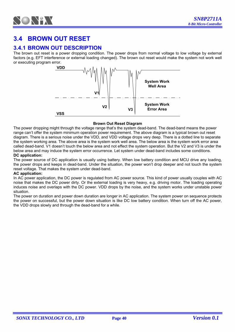
3.4 BROWN OUT RESET 3.4.1 BROWN OUT DESCRIPTION The brown out reset is a power dropping condition. The power drops from normal voltage to low voltage by external factors (e.g. EFT interference or external loading changed). The brown out reset would make the system not work well or executing program error.
VDD
VSS
V1
V2V3
System WorkWell Area
System WorkError Area
Brown Out Reset Diagram The power dropping might through the voltage range that’s the system dead-band. The dead-band means the power range can’t offer the system minimum operation power requirement. The above diagram is a typical brown out reset diagram. There is a serious noise under the VDD, and VDD voltage drops very deep. There is a dotted line to separate the system working area. The above area is the system work well area. The below area is the system work error area called dead-band. V1 doesn’t touch the below area and not effect the system operation. But the V2 and V3 is under the below area and may induce the system error occurrence. Let system under dead-band includes some conditions. DC application: The power source of DC application is usually using battery. When low battery condition and MCU drive any loading, the power drops and keeps in dead-band. Under the situation, the power won’t drop deeper and not touch the system reset voltage. That makes the system under dead-band. AC application: In AC power application, the DC power is regulated from AC power source. This kind of power usually couples with AC noise that makes the DC power dirty. Or the external loading is very heavy, e.g. driving motor. The loading operating induces noise and overlaps with the DC power. VDD drops by the noise, and the system works under unstable power situation. The power on duration and power down duration are longer in AC application. The system power on sequence protects the power on successful, but the power down situation is like DC low battery condition. When turn off the AC power, the VDD drops slowly and through the dead-band for a while.
SN8P2711A 8-Bit Micro-Controller
SONiX TECHNOLOGY CO., LTD Page 41 Version 0.1
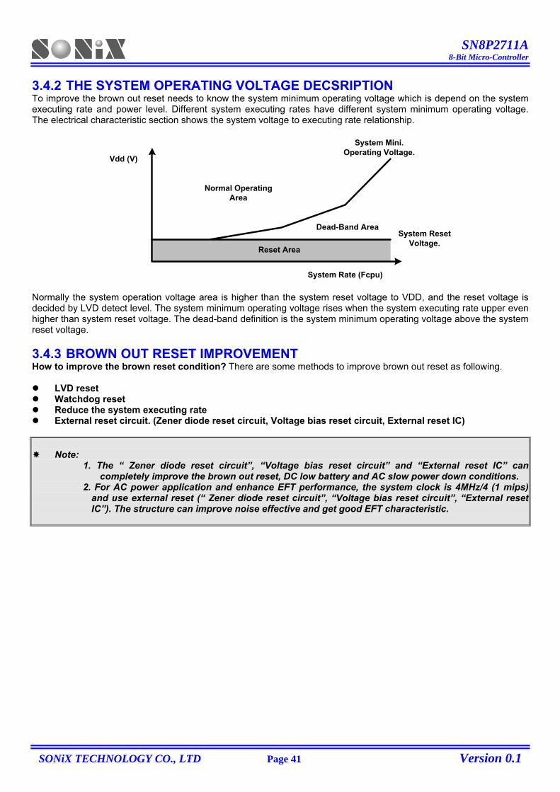
3.4.2 THE SYSTEM OPERATING VOLTAGE DECSRIPTION To improve the brown out reset needs to know the system minimum operating voltage which is depend on the system executing rate and power level. Different system executing rates have different system minimum operating voltage. The electrical characteristic section shows the system voltage to executing rate relationship.
Vdd (V)
System Rate (Fcpu)
System Mini.Operating Voltage.
System ResetVoltage.
Dead-Band Area
Normal OperatingArea
Reset Area
Normally the system operation voltage area is higher than the system reset voltage to VDD, and the reset voltage is decided by LVD detect level. The system minimum operating voltage rises when the system executing rate upper even higher than system reset voltage. The dead-band definition is the system minimum operating voltage above the system reset voltage. 3.4.3 BROWN OUT RESET IMPROVEMENT How to improve the brown reset condition? There are some methods to improve brown out reset as following.
LVD reset Watchdog reset Reduce the system executing rate External reset circuit. (Zener diode reset circuit, Voltage bias reset circuit, External reset IC)
Note: 1. The “ Zener diode reset circuit”, “Voltage bias reset circuit” and “External reset IC” can
completely improve the brown out reset, DC low battery and AC slow power down conditions. 2. For AC power application and enhance EFT performance, the system clock is 4MHz/4 (1 mips)
and use external reset (“ Zener diode reset circuit”, “Voltage bias reset circuit”, “External reset IC”). The structure can improve noise effective and get good EFT characteristic.
SN8P2711A 8-Bit Micro-Controller
SONiX TECHNOLOGY CO., LTD Page 42 Version 0.1
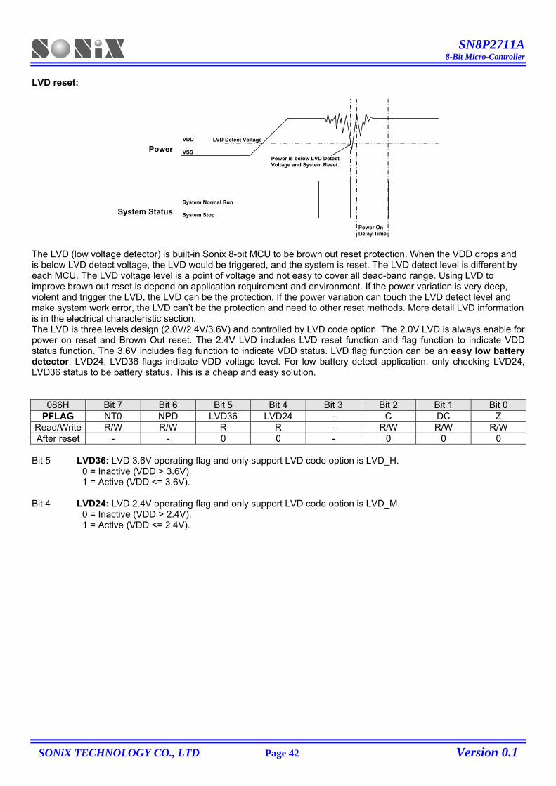
LVD reset:
VDD
VSS
System Normal Run
System Stop
LVD Detect Voltage
Power OnDelay Time
Power
System Status
Power is below LVD DetectVoltage and System Reset.
The LVD (low voltage detector) is built-in Sonix 8-bit MCU to be brown out reset protection. When the VDD drops and is below LVD detect voltage, the LVD would be triggered, and the system is reset. The LVD detect level is different by each MCU. The LVD voltage level is a point of voltage and not easy to cover all dead-band range. Using LVD to improve brown out reset is depend on application requirement and environment. If the power variation is very deep, violent and trigger the LVD, the LVD can be the protection. If the power variation can touch the LVD detect level and make system work error, the LVD can’t be the protection and need to other reset methods. More detail LVD information is in the electrical characteristic section. The LVD is three levels design (2.0V/2.4V/3.6V) and controlled by LVD code option. The 2.0V LVD is always enable for power on reset and Brown Out reset. The 2.4V LVD includes LVD reset function and flag function to indicate VDD status function. The 3.6V includes flag function to indicate VDD status. LVD flag function can be an easy low battery detector. LVD24, LVD36 flags indicate VDD voltage level. For low battery detect application, only checking LVD24, LVD36 status to be battery status. This is a cheap and easy solution.
086H Bit 7 Bit 6 Bit 5 Bit 4 Bit 3 Bit 2 Bit 1 Bit 0 PFLAG NT0 NPD LVD36 LVD24 - C DC Z
Read/Write R/W R/W R R - R/W R/W R/W After reset - - 0 0 - 0 0 0
Bit 5 LVD36: LVD 3.6V operating flag and only support LVD code option is LVD_H.
0 = Inactive (VDD > 3.6V). 1 = Active (VDD <= 3.6V).
Bit 4 LVD24: LVD 2.4V operating flag and only support LVD code option is LVD_M. 0 = Inactive (VDD > 2.4V). 1 = Active (VDD <= 2.4V).
SN8P2711A 8-Bit Micro-Controller
SONiX TECHNOLOGY CO., LTD Page 43 Version 0.1
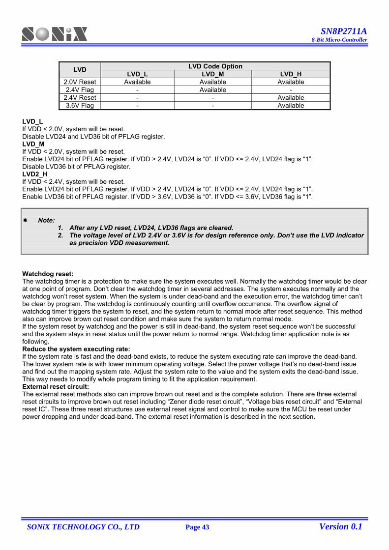
LVD Code Option LVD LVD_L LVD_M LVD_H 2.0V Reset Available Available Available 2.4V Flag - Available -
2.4V Reset - - Available 3.6V Flag - - Available
LVD_L If VDD < 2.0V, system will be reset. Disable LVD24 and LVD36 bit of PFLAG register. LVD_M If VDD < 2.0V, system will be reset. Enable LVD24 bit of PFLAG register. If VDD > 2.4V, LVD24 is “0”. If VDD <= 2.4V, LVD24 flag is “1”. Disable LVD36 bit of PFLAG register. LVD2_H If VDD < 2.4V, system will be reset. Enable LVD24 bit of PFLAG register. If VDD > 2.4V, LVD24 is “0”. If VDD <= 2.4V, LVD24 flag is “1”. Enable LVD36 bit of PFLAG register. If VDD > 3.6V, LVD36 is “0”. If VDD <= 3.6V, LVD36 flag is “1”.
Note: 1. After any LVD reset, LVD24, LVD36 flags are cleared. 2. The voltage level of LVD 2.4V or 3.6V is for design reference only. Don’t use the LVD indicator
as precision VDD measurement.
Watchdog reset: The watchdog timer is a protection to make sure the system executes well. Normally the watchdog timer would be clear at one point of program. Don’t clear the watchdog timer in several addresses. The system executes normally and the watchdog won’t reset system. When the system is under dead-band and the execution error, the watchdog timer can’t be clear by program. The watchdog is continuously counting until overflow occurrence. The overflow signal of watchdog timer triggers the system to reset, and the system return to normal mode after reset sequence. This method also can improve brown out reset condition and make sure the system to return normal mode. If the system reset by watchdog and the power is still in dead-band, the system reset sequence won’t be successful and the system stays in reset status until the power return to normal range. Watchdog timer application note is as following. Reduce the system executing rate: If the system rate is fast and the dead-band exists, to reduce the system executing rate can improve the dead-band. The lower system rate is with lower minimum operating voltage. Select the power voltage that’s no dead-band issue and find out the mapping system rate. Adjust the system rate to the value and the system exits the dead-band issue. This way needs to modify whole program timing to fit the application requirement. External reset circuit: The external reset methods also can improve brown out reset and is the complete solution. There are three external reset circuits to improve brown out reset including “Zener diode reset circuit”, “Voltage bias reset circuit” and “External reset IC”. These three reset structures use external reset signal and control to make sure the MCU be reset under power dropping and under dead-band. The external reset information is described in the next section.
SN8P2711A 8-Bit Micro-Controller
SONiX TECHNOLOGY CO., LTD Page 44 Version 0.1
3.5 EXTERNAL RESET External reset function is controlled by “Reset_Pin” code option. Set the code option as “Reset” option to enable external reset function. External reset pin is Schmitt Trigger structure and low level active. The system is running when reset pin is high level voltage input. The reset pin receives the low voltage and the system is reset. The external reset operation actives in power on and normal running mode. During system power-up, the external reset pin must be high level input, or the system keeps in reset status. External reset sequence is as following.
External reset (only external reset pin enable): System checks external reset pin status. If external reset pin is not high level, the system keeps reset status and waits external reset pin released.
System initialization: All system registers is set as initial conditions and system is ready. Oscillator warm up: Oscillator operation is successfully and supply to system clock. Program executing: Power on sequence is finished and program executes from ORG 0.
The external reset can reset the system during power on duration, and good external reset circuit can protect the system to avoid working at unusual power condition, e.g. brown out reset in AC power application…
3.6 EXTERNAL RESET CIRCUIT 3.6.1 Simply RC Reset Circuit
MCU
VDD
VSS
VCC
GND
RST
R147K ohm
C10.1uF
R2
100 ohm
This is the basic reset circuit, and only includes R1 and C1. The RC circuit operation makes a slow rising signal into reset pin as power up. The reset signal is slower than VDD power up timing, and system occurs a power on signal from the timing difference.
Note: The reset circuit is no any protection against unusual power or brown out reset.
SN8P2711A 8-Bit Micro-Controller
SONiX TECHNOLOGY CO., LTD Page 45 Version 0.1
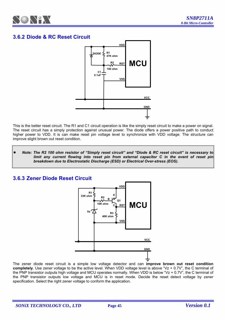
3.6.2 Diode & RC Reset Circuit
MCU
VDD
VSS
VCC
GND
RST
R147K ohm
C10.1uF
DIODE
R2
100 ohm
This is the better reset circuit. The R1 and C1 circuit operation is like the simply reset circuit to make a power on signal. The reset circuit has a simply protection against unusual power. The diode offers a power positive path to conduct higher power to VDD. It is can make reset pin voltage level to synchronize with VDD voltage. The structure can improve slight brown out reset condition.
Note: The R2 100 ohm resistor of “Simply reset circuit” and “Diode & RC reset circuit” is necessary to limit any current flowing into reset pin from external capacitor C in the event of reset pin breakdown due to Electrostatic Discharge (ESD) or Electrical Over-stress (EOS).
3.6.3 Zener Diode Reset Circuit
MCU
VDD
VSS
VCC
GND
RST
R133K ohm
R340K ohm
R2
10K ohm
Vz
Q1
E
C
B
The zener diode reset circuit is a simple low voltage detector and can improve brown out reset condition completely. Use zener voltage to be the active level. When VDD voltage level is above “Vz + 0.7V”, the C terminal of the PNP transistor outputs high voltage and MCU operates normally. When VDD is below “Vz + 0.7V”, the C terminal of the PNP transistor outputs low voltage and MCU is in reset mode. Decide the reset detect voltage by zener specification. Select the right zener voltage to conform the application.
SN8P2711A 8-Bit Micro-Controller
SONiX TECHNOLOGY CO., LTD Page 46 Version 0.1
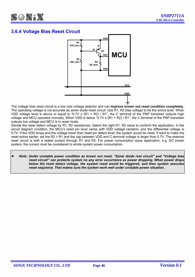
3.6.4 Voltage Bias Reset Circuit
MCU
VDD
VSS
VCC
GND
RST
R147K ohm
R32K ohm
R210K ohm
Q1
E
C
B
The voltage bias reset circuit is a low cost voltage detector and can improve brown out reset condition completely. The operating voltage is not accurate as zener diode reset circuit. Use R1, R2 bias voltage to be the active level. When VDD voltage level is above or equal to “0.7V x (R1 + R2) / R1”, the C terminal of the PNP transistor outputs high voltage and MCU operates normally. When VDD is below “0.7V x (R1 + R2) / R1”, the C terminal of the PNP transistor outputs low voltage and MCU is in reset mode. Decide the reset detect voltage by R1, R2 resistances. Select the right R1, R2 value to conform the application. In the circuit diagram condition, the MCU’s reset pin level varies with VDD voltage variation, and the differential voltage is 0.7V. If the VDD drops and the voltage lower than reset pin detect level, the system would be reset. If want to make the reset active earlier, set the R2 > R1 and the cap between VDD and C terminal voltage is larger than 0.7V. The external reset circuit is with a stable current through R1 and R2. For power consumption issue application, e.g. DC power system, the current must be considered to whole system power consumption.
Note: Under unstable power condition as brown out reset, “Zener diode rest circuit” and “Voltage bias reset circuit” can protects system no any error occurrence as power dropping. When power drops below the reset detect voltage, the system reset would be triggered, and then system executes reset sequence. That makes sure the system work well under unstable power situation.
SN8P2711A 8-Bit Micro-Controller
SONiX TECHNOLOGY CO., LTD Page 47 Version 0.1
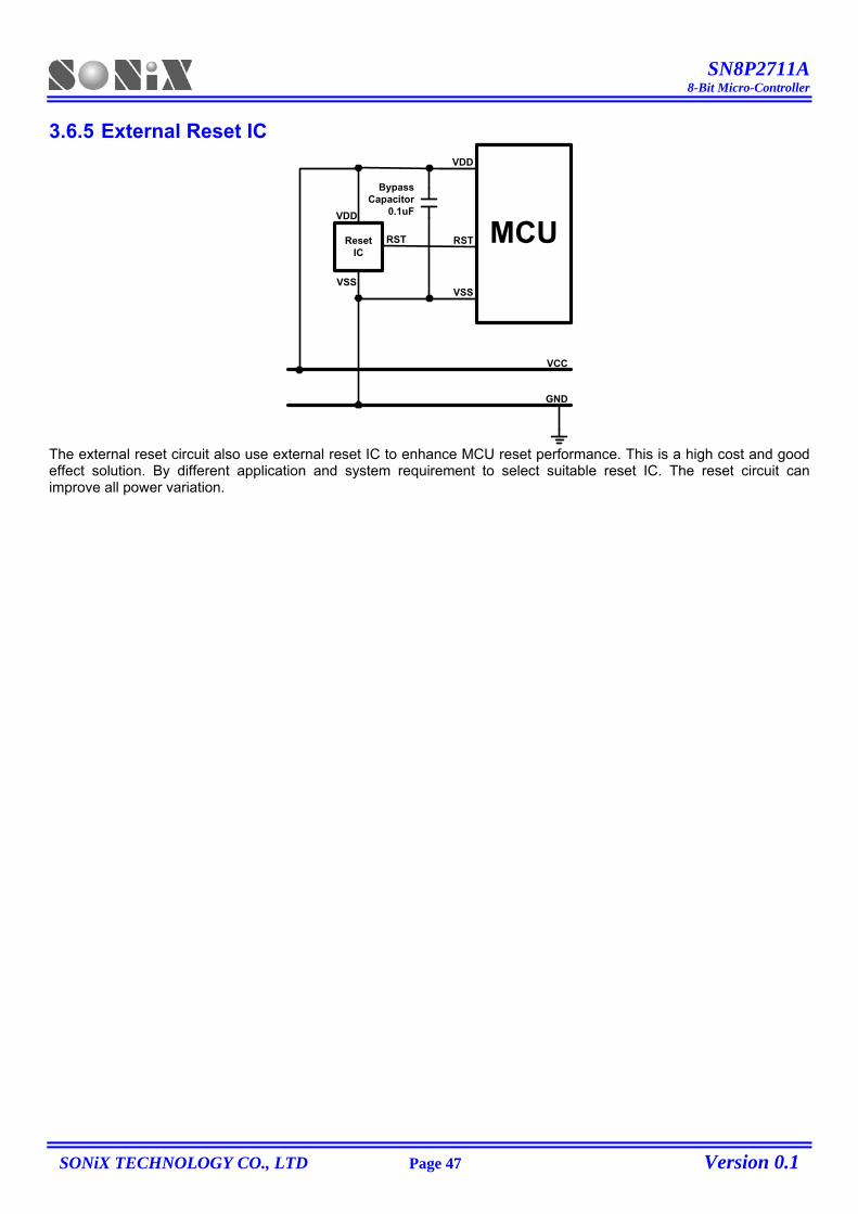
3.6.5 External Reset IC
MCU
VDD
VSS
VCC
GND
RSTResetIC
VDD
VSS
RST
BypassCapacitor
0.1uF
The external reset circuit also use external reset IC to enhance MCU reset performance. This is a high cost and good effect solution. By different application and system requirement to select suitable reset IC. The reset circuit can improve all power variation.
SN8P2711A 8-Bit Micro-Controller
SONiX TECHNOLOGY CO., LTD Page 48 Version 0.1
444 SYSTEM CLOCK
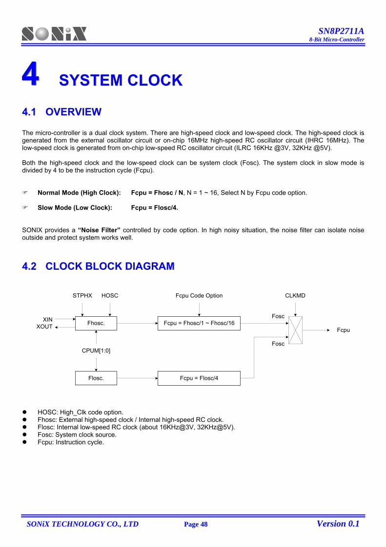
4.1 OVERVIEW The micro-controller is a dual clock system. There are high-speed clock and low-speed clock. The high-speed clock is generated from the external oscillator circuit or on-chip 16MHz high-speed RC oscillator circuit (IHRC 16MHz). The low-speed clock is generated from on-chip low-speed RC oscillator circuit (ILRC 16KHz @3V, 32KHz @5V). Both the high-speed clock and the low-speed clock can be system clock (Fosc). The system clock in slow mode is divided by 4 to be the instruction cycle (Fcpu).
Normal Mode (High Clock): Fcpu = Fhosc / N, N = 1 ~ 16, Select N by Fcpu code option.
Slow Mode (Low Clock): Fcpu = Flosc/4. SONIX provides a “Noise Filter” controlled by code option. In high noisy situation, the noise filter can isolate noise outside and protect system works well.
4.2 CLOCK BLOCK DIAGRAM
Fhosc. Fcpu = Fhosc/1 ~ Fhosc/16
Flosc. Fcpu = Flosc/4
CPUM[1:0]
XINXOUT
STPHX HOSC Fcpu Code Option
Fosc
Fosc
CLKMD
Fcpu
HOSC: High_Clk code option. Fhosc: External high-speed clock / Internal high-speed RC clock. Flosc: Internal low-speed RC clock (about 16KHz@3V, 32KHz@5V). Fosc: System clock source. Fcpu: Instruction cycle.
SN8P2711A 8-Bit Micro-Controller
SONiX TECHNOLOGY CO., LTD Page 49 Version 0.1
4.3 OSCM REGISTER The OSCM register is an oscillator control register. It controls oscillator status, system mode.
0CAH Bit 7 Bit 6 Bit 5 Bit 4 Bit 3 Bit 2 Bit 1 Bit 0 OSCM 0 0 0 CPUM1 CPUM0 CLKMD STPHX 0
Read/Write - - - R/W R/W R/W R/W - After reset - - - 0 0 0 0 -
Bit 1 STPHX: External high-speed oscillator control bit.
0 = External high-speed oscillator free run. 1 = External high-speed oscillator free run stop. Internal low-speed RC oscillator is still running.
Bit 2 CLKMD: System high/Low clock mode control bit.
0 = Normal (dual) mode. System clock is high clock. 1 = Slow mode. System clock is internal low clock.
Bit[4:3] CPUM[1:0]: CPU operating mode control bits.
00 = normal. 01 = sleep (power down) mode. 10 = green mode. 11 = reserved.
Example: Stop high-speed oscillator B0BSET FSTPHX ; To stop external high-speed oscillator only.
Example: When entering the power down mode (sleep mode), both high-speed oscillator and internal low-speed oscillator will be stopped.
B0BSET FCPUM0 ; To stop external high-speed oscillator and internal low-speed ; oscillator called power down mode (sleep mode).
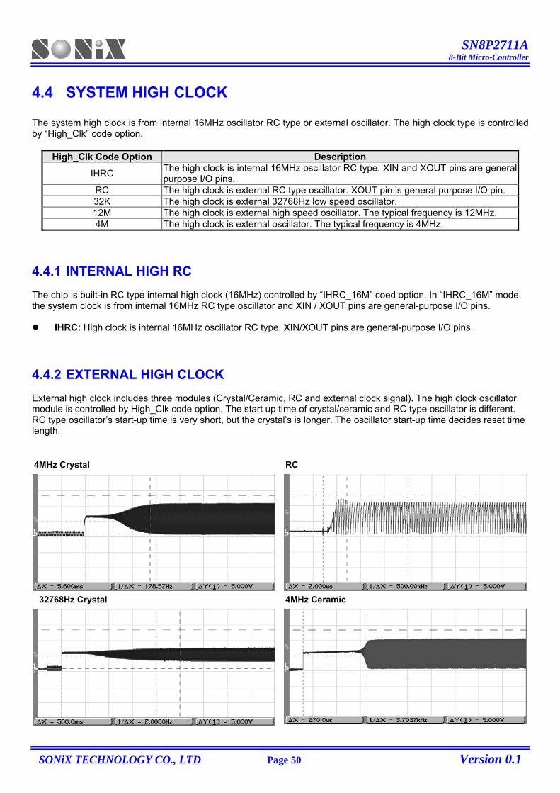
SN8P2711A 8-Bit Micro-Controller
SONiX TECHNOLOGY CO., LTD Page 50 Version 0.1
4.4 SYSTEM HIGH CLOCK The system high clock is from internal 16MHz oscillator RC type or external oscillator. The high clock type is controlled by “High_Clk” code option.
High_Clk Code Option Description
IHRC The high clock is internal 16MHz oscillator RC type. XIN and XOUT pins are general purpose I/O pins.
RC The high clock is external RC type oscillator. XOUT pin is general purpose I/O pin. 32K The high clock is external 32768Hz low speed oscillator. 12M The high clock is external high speed oscillator. The typical frequency is 12MHz. 4M The high clock is external oscillator. The typical frequency is 4MHz.
4.4.1 INTERNAL HIGH RC The chip is built-in RC type internal high clock (16MHz) controlled by “IHRC_16M” coed option. In “IHRC_16M” mode, the system clock is from internal 16MHz RC type oscillator and XIN / XOUT pins are general-purpose I/O pins.
IHRC: High clock is internal 16MHz oscillator RC type. XIN/XOUT pins are general-purpose I/O pins.
4.4.2 EXTERNAL HIGH CLOCK External high clock includes three modules (Crystal/Ceramic, RC and external clock signal). The high clock oscillator module is controlled by High_Clk code option. The start up time of crystal/ceramic and RC type oscillator is different. RC type oscillator’s start-up time is very short, but the crystal’s is longer. The oscillator start-up time decides reset time length.
RC
4MHz Ceramic
4MHz Crystal
32768Hz Crystal
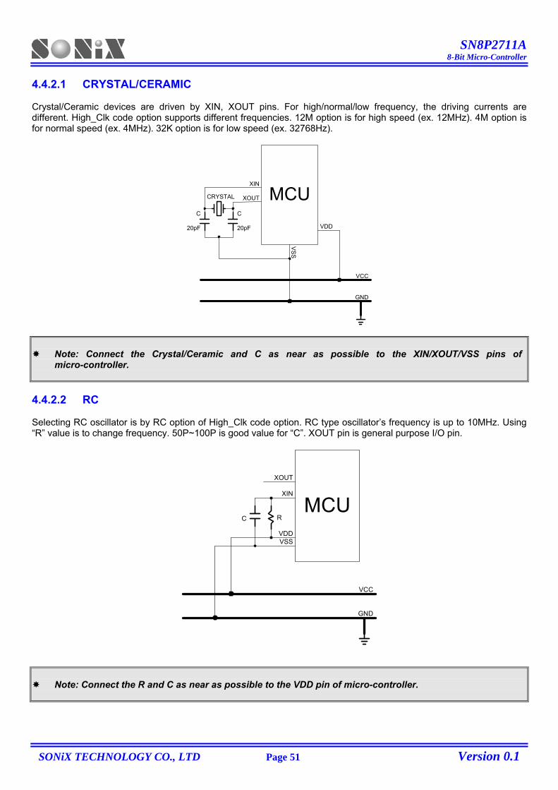
SN8P2711A 8-Bit Micro-Controller
SONiX TECHNOLOGY CO., LTD Page 51 Version 0.1
4.4.2.1 CRYSTAL/CERAMIC Crystal/Ceramic devices are driven by XIN, XOUT pins. For high/normal/low frequency, the driving currents are different. High_Clk code option supports different frequencies. 12M option is for high speed (ex. 12MHz). 4M option is for normal speed (ex. 4MHz). 32K option is for low speed (ex. 32768Hz).
MCU
VCC
GND
C
20pF
XIN
XOUT
VDD
VS
S
C
20pF
CRYSTAL
Note: Connect the Crystal/Ceramic and C as near as possible to the XIN/XOUT/VSS pins of micro-controller.
4.4.2.2 RC Selecting RC oscillator is by RC option of High_Clk code option. RC type oscillator’s frequency is up to 10MHz. Using “R” value is to change frequency. 50P~100P is good value for “C”. XOUT pin is general purpose I/O pin.
RMCU
VCC
GND
XIN
XOUT
VDDVSS
C
Note: Connect the R and C as near as possible to the VDD pin of micro-controller.
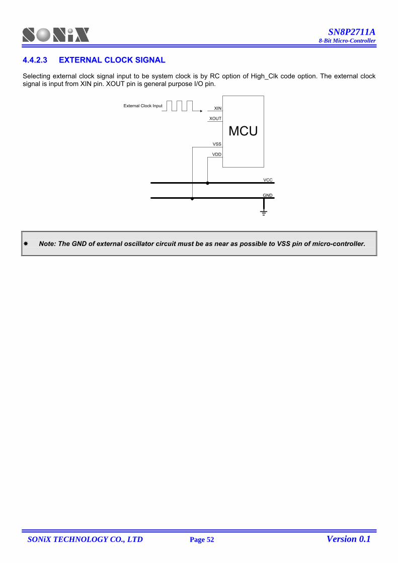
SN8P2711A 8-Bit Micro-Controller
SONiX TECHNOLOGY CO., LTD Page 52 Version 0.1
4.4.2.3 EXTERNAL CLOCK SIGNAL Selecting external clock signal input to be system clock is by RC option of High_Clk code option. The external clock signal is input from XIN pin. XOUT pin is general purpose I/O pin.
MCU
VCC
GND
VSS
VDD
XIN
XOUT
External Clock Input
Note: The GND of external oscillator circuit must be as near as possible to VSS pin of micro-controller.
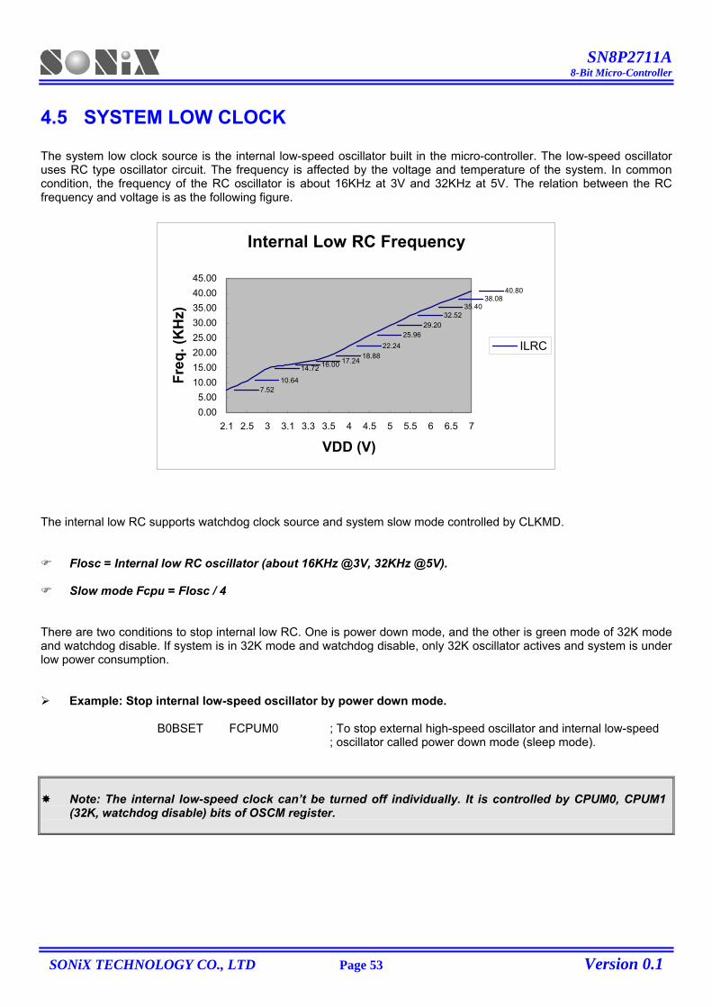
SN8P2711A 8-Bit Micro-Controller
SONiX TECHNOLOGY CO., LTD Page 53 Version 0.1
4.5 SYSTEM LOW CLOCK The system low clock source is the internal low-speed oscillator built in the micro-controller. The low-speed oscillator uses RC type oscillator circuit. The frequency is affected by the voltage and temperature of the system. In common condition, the frequency of the RC oscillator is about 16KHz at 3V and 32KHz at 5V. The relation between the RC frequency and voltage is as the following figure.
Internal Low RC Frequency
7.5210.64
14.72 16.00 17.2418.88
22.2425.96
29.2032.52
35.4038.08
40.80
0.005.00
10.0015.0020.0025.0030.0035.0040.0045.00
2.1 2.5 3 3.1 3.3 3.5 4 4.5 5 5.5 6 6.5 7
VDD (V)
Freq
. (K
Hz)
ILRC
The internal low RC supports watchdog clock source and system slow mode controlled by CLKMD.
Flosc = Internal low RC oscillator (about 16KHz @3V, 32KHz @5V).
Slow mode Fcpu = Flosc / 4 There are two conditions to stop internal low RC. One is power down mode, and the other is green mode of 32K mode and watchdog disable. If system is in 32K mode and watchdog disable, only 32K oscillator actives and system is under low power consumption.
Example: Stop internal low-speed oscillator by power down mode. B0BSET FCPUM0 ; To stop external high-speed oscillator and internal low-speed ; oscillator called power down mode (sleep mode).
Note: The internal low-speed clock can’t be turned off individually. It is controlled by CPUM0, CPUM1 (32K, watchdog disable) bits of OSCM register.
SN8P2711A 8-Bit Micro-Controller
SONiX TECHNOLOGY CO., LTD Page 54 Version 0.1
4.5.1 SYSTEM CLOCK MEASUREMENT Under design period, the users can measure system clock speed by software instruction cycle (Fcpu). This way is useful in RC mode.
Example: Fcpu instruction cycle of external oscillator. B0BSET P0M.0 ; Set P0.0 to be output mode for outputting Fcpu toggle signal. @@: B0BSET P0.0 ; Output Fcpu toggle signal in low-speed clock mode. B0BCLR P0.0 ; Measure the Fcpu frequency by oscilloscope. JMP @B
Note: Do not measure the RC frequency directly from XIN; the probe impendence will affect the RC frequency.

SN8P2711A 8-Bit Micro-Controller
SONiX TECHNOLOGY CO., LTD Page 55 Version 0.1
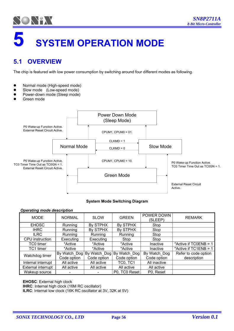
SN8P2711A 8-Bit Micro-Controller
SONiX TECHNOLOGY CO., LTD Page 56 Version 0.1
555 SYSTEM OPERATION MODE 5.1 OVERVIEW The chip is featured with low power consumption by switching around four different modes as following.
Normal mode (High-speed mode) Slow mode (Low-speed mode) Power-down mode (Sleep mode) Green mode
Power Down Mode(Sleep Mode)
Slow Mode
Green Mode
Normal ModeCLKMD = 1
CLKMD = 0
P0 Wake-up Function Active.External Reset Circuit Active. CPUM1, CPUM0 = 01.
CPUM1, CPUM0 = 10. P0 Wake-up Function Active.TC0 Timer Time Out as TC0GN = 1.
External Reset CircuitActive.
P0 Wake-up Function Active.TC0 Timer Time Out as TC0GN = 1.
External Reset Circuit Active.
System Mode Switching Diagram
Operating mode description
MODE NORMAL SLOW GREEN POWER DOWN (SLEEP) REMARK
EHOSC Running By STPHX By STPHX Stop IHRC Running By STPHX By STPHX Stop ILRC Running Running Running Stop
CPU instruction Executing Executing Stop Stop TC0 timer *Active *Active *Active Inactive *Active if TC0ENB = 1TC1 timer *Active *Active *Active Inactive *Active if TC1ENB = 1
Watchdog timer By Watch_Dog Code option
By Watch_DogCode option
By Watch_Dog Code option
By Watch_Dog Code option
Refer to code option description
Internal interrupt All active All active TC0, TC1 All inactive External interrupt All active All active All active All active Wakeup source - - P0, TC0 Reset P0, Reset
EHOSC: External high clock IHRC: Internal high clock (16M RC oscillator) ILRC: Internal low clock (16K RC oscillator at 3V, 32K at 5V)
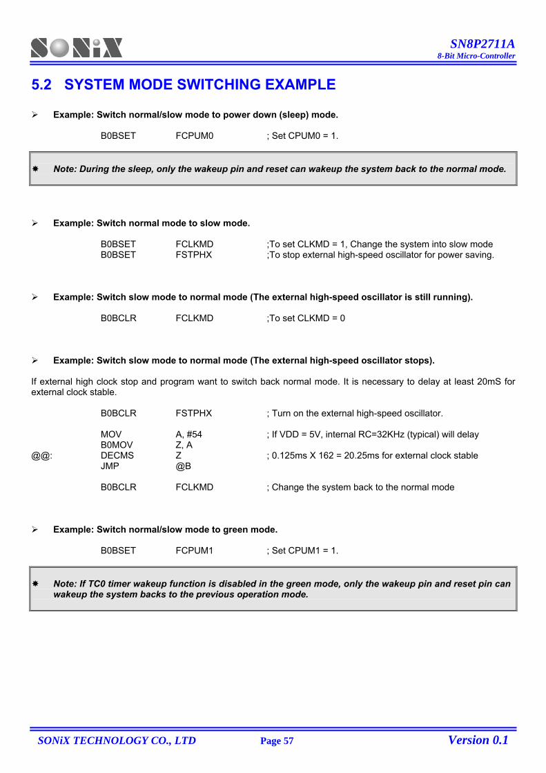
SN8P2711A 8-Bit Micro-Controller
SONiX TECHNOLOGY CO., LTD Page 57 Version 0.1
5.2 SYSTEM MODE SWITCHING EXAMPLE
Example: Switch normal/slow mode to power down (sleep) mode. B0BSET FCPUM0 ; Set CPUM0 = 1.
Note: During the sleep, only the wakeup pin and reset can wakeup the system back to the normal mode.
Example: Switch normal mode to slow mode. B0BSET FCLKMD ;To set CLKMD = 1, Change the system into slow mode B0BSET FSTPHX ;To stop external high-speed oscillator for power saving.
Example: Switch slow mode to normal mode (The external high-speed oscillator is still running). B0BCLR FCLKMD ;To set CLKMD = 0
Example: Switch slow mode to normal mode (The external high-speed oscillator stops). If external high clock stop and program want to switch back normal mode. It is necessary to delay at least 20mS for external clock stable. B0BCLR FSTPHX ; Turn on the external high-speed oscillator. MOV A, #54 ; If VDD = 5V, internal RC=32KHz (typical) will delay B0MOV Z, A @@: DECMS Z ; 0.125ms X 162 = 20.25ms for external clock stable JMP @B B0BCLR FCLKMD ; Change the system back to the normal mode
Example: Switch normal/slow mode to green mode. B0BSET FCPUM1 ; Set CPUM1 = 1.
Note: If TC0 timer wakeup function is disabled in the green mode, only the wakeup pin and reset pin can wakeup the system backs to the previous operation mode.
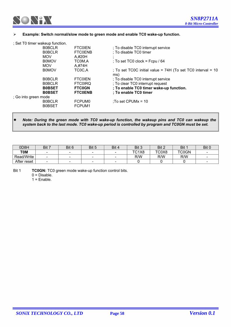
SN8P2711A 8-Bit Micro-Controller
SONiX TECHNOLOGY CO., LTD Page 58 Version 0.1
Example: Switch normal/slow mode to green mode and enable TC0 wake-up function.
; Set T0 timer wakeup function. B0BCLR FTC0IEN ; To disable TC0 interrupt service B0BCLR FTC0ENB ; To disable TC0 timer MOV A,#20H ; B0MOV TC0M,A ; To set TC0 clock = Fcpu / 64 MOV A,#74H B0MOV TC0C,A ; To set TC0C initial value = 74H (To set TC0 interval = 10
ms) B0BCLR FTC0IEN ; To disable TC0 interrupt service B0BCLR FTC0IRQ ; To clear TC0 interrupt request B0BSET FTC0GN ; To enable TC0 timer wake-up function. B0BSET FTC0ENB ; To enable TC0 timer ; Go into green mode B0BCLR FCPUM0 ;To set CPUMx = 10 B0BSET FCPUM1
Note: During the green mode with TC0 wake-up function, the wakeup pins and TC0 can wakeup the system back to the last mode. TC0 wake-up period is controlled by program and TC0GN must be set.
0D8H Bit 7 Bit 6 Bit 5 Bit 4 Bit 3 Bit 2 Bit 1 Bit 0 T0M - - - - TC1X8 TC0X8 TC0GN -
Read/Write - - - - R/W R/W R/W - After reset - - - - 0 0 0 -
Bit 1 TC0GN: TC0 green mode wake-up function control bits.
0 = Disable. 1 = Enable.
SN8P2711A 8-Bit Micro-Controller
SONiX TECHNOLOGY CO., LTD Page 59 Version 0.1
5.3 WAKEUP 5.3.1 OVERVIEW Under power down mode (sleep mode) or green mode, program doesn’t execute. The wakeup trigger can wake the system up to normal mode or slow mode. The wakeup trigger sources are external trigger (P0 level change) and internal trigger (TC0 timer overflow).
Power down mode is waked up to normal mode. The wakeup trigger is only external trigger (P0 level change) Green mode is waked up to last mode (normal mode or slow mode). The wakeup triggers are external trigger (P0
level change) and internal trigger (TC0 timer overflow). 5.3.2 WAKEUP TIME When the system is in power down mode (sleep mode), the high clock oscillator stops. When waked up from power down mode, MCU waits for 2048 external high-speed oscillator clocks as the wakeup time to stable the oscillator circuit. After the wakeup time, the system goes into the normal mode.
Note: Wakeup from green mode is no wakeup time because the clock doesn’t stop in green mode. The value of the wakeup time is as the following.
The Wakeup time = 1/Fosc * 2048 (sec) + high clock start-up time
Note: The high clock start-up time is depended on the VDD and oscillator type of high clock.
Example: In power down mode (sleep mode), the system is waked up. After the wakeup time, the system goes into normal mode. The wakeup time is as the following.
The wakeup time = 1/Fosc * 2048 = 0.512 ms (Fosc = 4MHz)
The total wakeup time = 0.512ms + oscillator start-up time
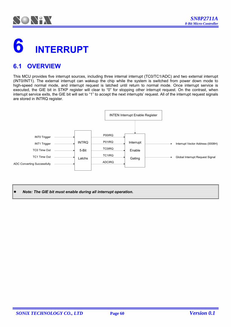
SN8P2711A 8-Bit Micro-Controller
SONiX TECHNOLOGY CO., LTD Page 60 Version 0.1
666 INTERRUPT 6.1 OVERVIEW This MCU provides five interrupt sources, including three internal interrupt (TC0/TC1/ADC) and two external interrupt (INT0/INT1). The external interrupt can wakeup the chip while the system is switched from power down mode to high-speed normal mode, and interrupt request is latched until return to normal mode. Once interrupt service is executed, the GIE bit in STKP register will clear to “0” for stopping other interrupt request. On the contrast, when interrupt service exits, the GIE bit will set to “1” to accept the next interrupts’ request. All of the interrupt request signals are stored in INTRQ register.
INTEN Interrupt Enable Register
Interrupt
Enable
Gating
INTRQ
5-Bit
Latchs
P00IRQ
P01IRQ
TC0IRQ
TC1IRQ
ADCIRQ
Interrupt Vector Address (0008H)
Global Interrupt Request Signal
INT0 Trigger
INT1 Trigger
TC0 Time Out
TC1 Time Out
ADC Converting Successfully
Note: The GIE bit must enable during all interrupt operation.
SN8P2711A 8-Bit Micro-Controller
SONiX TECHNOLOGY CO., LTD Page 61 Version 0.1
6.2 INTEN INTERRUPT ENABLE REGISTER INTEN is the interrupt request control register including three internal interrupts, two external interrupts enable control bits. One of the register to be set “1” is to enable the interrupt request function. Once of the interrupt occur, the stack is incremented and program jump to ORG 8 to execute interrupt service routines. The program exits the interrupt service routine when the returning interrupt service routine instruction (RETI) is executed.
0C9H Bit 7 Bit 6 Bit 5 Bit 4 Bit 3 Bit 2 Bit 1 Bit 0 INTEN ADCIEN TC1IEN TC0IEN - - - P01IEN P00IEN
Read/Write R/W R/W R/W - - - R/W R/W After reset 0 0 0 - - - 0 0
Bit 0 P00IEN: External P0.0 interrupt (INT0) control bit.
0 = Disable INT0 interrupt function. 1 = Enable INT0 interrupt function.
Bit 1 P01IEN: External P0.1 interrupt (INT1) control bit. 0 = Disable INT1 interrupt function. 1 = Enable INT1 interrupt function.
Bit 5 TC0IEN: TC0 timer interrupt control bit. 0 = Disable TC0 interrupt function. 1 = Enable TC0 interrupt function.
Bit 6 TC1IEN: TC1 timer interrupt control bit. 0 = Disable TC1 interrupt function. 1 = Enable TC1 interrupt function.
Bit 7 ADCIEN: ADC interrupt control bit. 0 = Disable ADC interrupt function. 1 = Enable ADC interrupt function.
SN8P2711A 8-Bit Micro-Controller
SONiX TECHNOLOGY CO., LTD Page 62 Version 0.1
6.3 INTRQ INTERRUPT REQUEST REGISTER INTRQ is the interrupt request flag register. The register includes all interrupt request indication flags. Each one of the interrupt requests occurs, the bit of the INTRQ register would be set “1”. The INTRQ value needs to be clear by programming after detecting the flag. In the interrupt vector of program, users know the any interrupt requests occurring by the register and do the routine corresponding of the interrupt request.
0C8H Bit 7 Bit 6 Bit 5 Bit 4 Bit 3 Bit 2 Bit 1 Bit 0 INTRQ ADCIRQ TC1IRQ TC0IRQ - - - P01IRQ P00IRQ
Read/Write R/W R/W R/W - - - R/W R/W After reset 0 0 0 - - - 0 0
Bit 0 P00IRQ: External P0.0 interrupt (INT0) request flag.
0 = None INT0 interrupt request. 1 = INT0 interrupt request.
Bit 1 P01IRQ: External P0.1 interrupt (INT1) request flag. 0 = None INT1 interrupt request. 1 = INT1 interrupt request.
Bit 5 TC0IRQ: TC0 timer interrupt request flag. 0 = None TC0 interrupt request. 1 = TC0 interrupt request.
Bit 6 TC1IRQ: TC1 timer interrupt request flag. 0 = None TC1 interrupt request. 1 = TC1 interrupt request.
Bit 7 ADCIRQ: ADC interrupt request flag.
0 = None ADC interrupt request. 1 = ADC interrupt request.
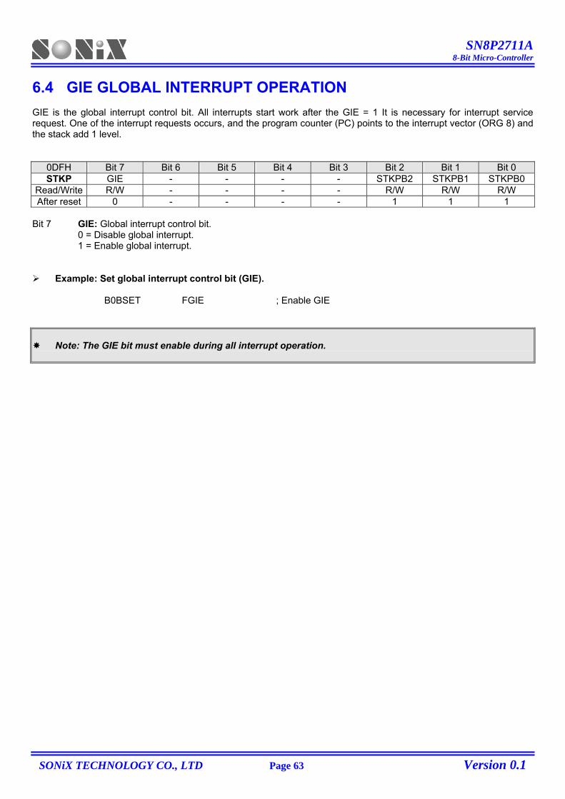
SN8P2711A 8-Bit Micro-Controller
SONiX TECHNOLOGY CO., LTD Page 63 Version 0.1
6.4 GIE GLOBAL INTERRUPT OPERATION GIE is the global interrupt control bit. All interrupts start work after the GIE = 1 It is necessary for interrupt service request. One of the interrupt requests occurs, and the program counter (PC) points to the interrupt vector (ORG 8) and the stack add 1 level.
0DFH Bit 7 Bit 6 Bit 5 Bit 4 Bit 3 Bit 2 Bit 1 Bit 0 STKP GIE - - - - STKPB2 STKPB1 STKPB0
Read/Write R/W - - - - R/W R/W R/W After reset 0 - - - - 1 1 1
Bit 7 GIE: Global interrupt control bit.
0 = Disable global interrupt. 1 = Enable global interrupt.
Example: Set global interrupt control bit (GIE). B0BSET FGIE ; Enable GIE
Note: The GIE bit must enable during all interrupt operation.
SN8P2711A 8-Bit Micro-Controller
SONiX TECHNOLOGY CO., LTD Page 64 Version 0.1
6.5 PUSH, POP ROUTINE When any interrupt occurs, system will jump to ORG 8 and execute interrupt service routine. It is necessary to save ACC, PFLAG data. The chip includes “PUSH”, “POP” for in/out interrupt service routine. The two instruction save and load ACC, PFLAG data into buffers and avoid main routine error after interrupt service routine finishing.
Note: ”PUSH”, “POP” instructions save and load ACC/PFLAG without (NT0, NPD). PUSH/POP buffer is an unique buffer and only one level.
Example: Store ACC and PAFLG data by PUSH, POP instructions when interrupt service routine executed. ORG 0 JMP START ORG 8 JMP INT_SERVICE ORG 10H START: … INT_SERVICE: PUSH ; Save ACC and PFLAG to buffers. … … POP ; Load ACC and PFLAG from buffers. RETI ; Exit interrupt service vector … ENDP
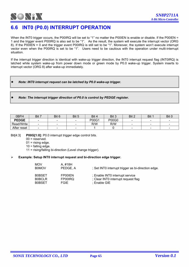
SN8P2711A 8-Bit Micro-Controller
SONiX TECHNOLOGY CO., LTD Page 65 Version 0.1
6.6 INT0 (P0.0) INTERRUPT OPERATION When the INT0 trigger occurs, the P00IRQ will be set to “1” no matter the P00IEN is enable or disable. If the P00IEN = 1 and the trigger event P00IRQ is also set to be “1”. As the result, the system will execute the interrupt vector (ORG 8). If the P00IEN = 0 and the trigger event P00IRQ is still set to be “1”. Moreover, the system won’t execute interrupt vector even when the P00IRQ is set to be “1”. Users need to be cautious with the operation under multi-interrupt situation. If the interrupt trigger direction is identical with wake-up trigger direction, the INT0 interrupt request flag (INT0IRQ) is latched while system wake-up from power down mode or green mode by P0.0 wake-up trigger. System inserts to interrupt vector (ORG 8) after wake-up immediately.
Note: INT0 interrupt request can be latched by P0.0 wake-up trigger.
Note: The interrupt trigger direction of P0.0 is control by PEDGE register.
0BFH Bit 7 Bit 6 Bit 5 Bit 4 Bit 3 Bit 2 Bit 1 Bit 0 PEDGE - - - P00G1 P00G0 - - -
Read/Write - - - R/W R/W - - - After reset - - - 1 0 - - -
Bit[4:3] P00G[1:0]: P0.0 interrupt trigger edge control bits.
00 = reserved. 01 = rising edge. 10 = falling edge. 11 = rising/falling bi-direction (Level change trigger).
Example: Setup INT0 interrupt request and bi-direction edge trigger.
MOV A, #18H B0MOV PEDGE, A ; Set INT0 interrupt trigger as bi-direction edge. B0BSET FP00IEN ; Enable INT0 interrupt service B0BCLR FP00IRQ ; Clear INT0 interrupt request flag B0BSET FGIE ; Enable GIE
SN8P2711A 8-Bit Micro-Controller
SONiX TECHNOLOGY CO., LTD Page 66 Version 0.1
Example: INT0 interrupt service routine.
ORG 8 ; Interrupt vector JMP INT_SERVICE INT_SERVICE: … ; Push routine to save ACC and PFLAG to buffers. B0BTS1 FP00IRQ ; Check P00IRQ JMP EXIT_INT ; P00IRQ = 0, exit interrupt vector B0BCLR FP00IRQ ; Reset P00IRQ … ; INT0 interrupt service routine … EXIT_INT: … ; Pop routine to load ACC and PFLAG from buffers. RETI ; Exit interrupt vector
SN8P2711A 8-Bit Micro-Controller
SONiX TECHNOLOGY CO., LTD Page 67 Version 0.1
6.7 INT1 (P0.1) INTERRUPT OPERATION When the INT1 trigger occurs, the P01IRQ will be set to “1” no matter the P01IEN is enable or disable. If the P01IEN = 1 and the trigger event P01IRQ is also set to be “1”. As the result, the system will execute the interrupt vector (ORG 8). If the P01IEN = 0 and the trigger event P01IRQ is still set to be “1”. Moreover, the system won’t execute interrupt vector even when the P01IRQ is set to be “1”. Users need to be cautious with the operation under multi-interrupt situation. If the interrupt trigger direction is identical with wake-up trigger direction, the INT1 interrupt request flag (INT1IRQ) is latched while system wake-up from power down mode or green mode by P0.1 wake-up trigger. System inserts to interrupt vector (ORG 8) after wake-up immediately.
Note: INT1 interrupt request can be latched by P0.1 wake-up trigger.
Note: The interrupt trigger direction of P0.1 is falling edge.
Example: INT1 interrupt request setup. B0BSET FP01IEN ; Enable INT1 interrupt service B0BCLR FP01IRQ ; Clear INT1 interrupt request flag B0BSET FGIE ; Enable GIE
Example: INT1 interrupt service routine. ORG 8 ; Interrupt vector JMP INT_SERVICE INT_SERVICE: … ; Push routine to save ACC and PFLAG to buffers. B0BTS1 FP01IRQ ; Check P01IRQ JMP EXIT_INT ; P01IRQ = 0, exit interrupt vector B0BCLR FP01IRQ ; Reset P01IRQ … ; INT1 interrupt service routine … EXIT_INT: … ; Pop routine to load ACC and PFLAG from buffers.
RETI ; Exit interrupt vector
SN8P2711A 8-Bit Micro-Controller
SONiX TECHNOLOGY CO., LTD Page 68 Version 0.1
6.8 TC0 INTERRUPT OPERATION When the TC0C counter overflows, the TC0IRQ will be set to “1” no matter the TC0IEN is enable or disable. If the TC0IEN and the trigger event TC0IRQ is set to be “1”. As the result, the system will execute the interrupt vector. If the TC0IEN = 0, the trigger event TC0IRQ is still set to be “1”. Moreover, the system won’t execute interrupt vector even when the TC0IEN is set to be “1”. Users need to be cautious with the operation under multi-interrupt situation.
Example: TC0 interrupt request setup. B0BCLR FTC0IEN ; Disable TC0 interrupt service B0BCLR FTC0ENB ; Disable TC0 timer MOV A, #20H ; B0MOV TC0M, A ; Set TC0 clock = Fcpu / 64 MOV A, #74H ; Set TC0C initial value = 74H B0MOV TC0C, A ; Set TC0 interval = 10 ms B0BSET FTC0IEN ; Enable TC0 interrupt service B0BCLR FTC0IRQ ; Clear TC0 interrupt request flag B0BSET FTC0ENB ; Enable TC0 timer B0BSET FGIE ; Enable GIE
Example: TC0 interrupt service routine. ORG 8 ; Interrupt vector JMP INT_SERVICE INT_SERVICE: … ; Push routine to save ACC and PFLAG to buffers.
B0BTS1 FTC0IRQ ; Check TC0IRQ JMP EXIT_INT ; TC0IRQ = 0, exit interrupt vector B0BCLR FTC0IRQ ; Reset TC0IRQ MOV A, #74H B0MOV TC0C, A ; Reset TC0C. … ; TC0 interrupt service routine … EXIT_INT: … ; Pop routine to load ACC and PFLAG from buffers. RETI ; Exit interrupt vector
SN8P2711A 8-Bit Micro-Controller
SONiX TECHNOLOGY CO., LTD Page 69 Version 0.1
6.9 TC1 INTERRUPT OPERATION When the TC1C counter overflows, the TC1IRQ will be set to “1” no matter the TC1IEN is enable or disable. If the TC1IEN and the trigger event TC1IRQ is set to be “1”. As the result, the system will execute the interrupt vector. If the TC1IEN = 0, the trigger event TC1IRQ is still set to be “1”. Moreover, the system won’t execute interrupt vector even when the TC1IEN is set to be “1”. Users need to be cautious with the operation under multi-interrupt situation. Example: TC1 interrupt request setup. B0BCLR FTC1IEN ; Disable TC1 interrupt service B0BCLR FTC1ENB ; Disable TC1 timer MOV A, #20H ; B0MOV TC1M, A ; Set TC1 clock = Fcpu / 64 MOV A, #74H ; Set TC1C initial value = 74H B0MOV TC1C, A ; Set TC1 interval = 10 ms B0BSET FTC1IEN ; Enable TC1 interrupt service B0BCLR FTC1IRQ ; Clear TC1 interrupt request flag B0BSET FTC1ENB ; Enable TC1 timer B0BSET FGIE ; Enable GIE Example: TC1 interrupt service routine. ORG 8 ; Interrupt vector JMP INT_SERVICE INT_SERVICE: … ; Push routine to save ACC and PFLAG to buffers.
B0BTS1 FTC1IRQ ; Check TC1IRQ JMP EXIT_INT ; TC1IRQ = 0, exit interrupt vector B0BCLR FTC1IRQ ; Reset TC1IRQ MOV A, #74H B0MOV TC1C, A ; Reset TC1C. … ; TC1 interrupt service routine … EXIT_INT: … ; Pop routine to load ACC and PFLAG from buffers. RETI ; Exit interrupt vector

SN8P2711A 8-Bit Micro-Controller
SONiX TECHNOLOGY CO., LTD Page 70 Version 0.1
SN8P2711A 8-Bit Micro-Controller
SONiX TECHNOLOGY CO., LTD Page 71 Version 0.1
6.10 ADC INTERRUPT OPERATION When the ADC converting successfully, the ADCIRQ will be set to “1” no matter the ADCIEN is enable or disable. If the ADCIEN and the trigger event ADCIRQ is set to be “1”. As the result, the system will execute the interrupt vector. If the ADCIEN = 0, the trigger event ADCIRQ is still set to be “1”. Moreover, the system won’t execute interrupt vector even when the ADCIEN is set to be “1”. Users need to be cautious with the operation under multi-interrupt situation.
Example: ADC interrupt request setup. B0BCLR FADCIEN ; Disable ADC interrupt service MOV A, #10110000B ; B0MOV ADM, A ; Enable P4.0 ADC input and ADC function. MOV A, #00000000B ; Set ADC converting rate = Fcpu/16 B0MOV ADR, A B0BSET FADCIEN ; Enable ADC interrupt service B0BCLR FADCIRQ ; Clear ADC interrupt request flag B0BSET FGIE ; Enable GIE B0BSET FADS ; Start ADC transformation
Example: ADC interrupt service routine. ORG 8 ; Interrupt vector JMP INT_SERVICE INT_SERVICE: … ; Push routine to save ACC and PFLAG to buffers.
B0BTS1 FADCIRQ ; Check ADCIRQ JMP EXIT_INT ; ADCIRQ = 0, exit interrupt vector B0BCLR FADCIRQ ; Reset ADCIRQ … ; ADC interrupt service routine … EXIT_INT: … ; Pop routine to load ACC and PFLAG from buffers. RETI ; Exit interrupt vector
SN8P2711A 8-Bit Micro-Controller
SONiX TECHNOLOGY CO., LTD Page 72 Version 0.1
6.11 MULTI-INTERRUPT OPERATION Under certain condition, the software designer uses more than one interrupt requests. Processing multi-interrupt request requires setting the priority of the interrupt requests. The IRQ flags of interrupts are controlled by the interrupt event. Nevertheless, the IRQ flag “1” doesn’t mean the system will execute the interrupt vector. In addition, which means the IRQ flags can be set “1” by the events without enable the interrupt. Once the event occurs, the IRQ will be logic “1”. The IRQ and its trigger event relationship is as the below table.
Interrupt Name Trigger Event Description P00IRQ P0.0 trigger controlled by PEDGE. P01IRQ P0.1 falling edge trigger. TC0IRQ TC0C overflow. TC1IRQ TC1C overflow. ADCIRQ ADC converting successfully.
For multi-interrupt conditions, two things need to be taking care of. One is to set the priority for these interrupt requests. Two is using IEN and IRQ flags to decide which interrupt to be executed. Users have to check interrupt control bit and interrupt request flag in interrupt routine.
Example: Check the interrupt request under multi-interrupt operation ORG 8 ; Interrupt vector JMP INT_SERVICE INT_SERVICE: … ; Push routine to save ACC and PFLAG to buffers. INTP00CHK: ; Check INT0 interrupt request B0BTS1 FP00IEN ; Check P00IEN JMP INTP01CHK ; Jump check to next interrupt B0BTS0 FP00IRQ ; Check P00IRQ JMP INTP00 ; Jump to INT0 interrupt service routine INTP01CHK: ; Check INT0 interrupt request B0BTS1 FP01IEN ; Check P01IEN JMP INTTC0CHK ; Jump check to next interrupt B0BTS0 FP01IRQ ; Check P01IRQ JMP INTP01 ; Jump to INT1 interrupt service routine INTTC0CHK: ; Check TC0 interrupt request B0BTS1 FTC0IEN ; Check TC0IEN JMP INTTC1CHK ; Jump check to next interrupt B0BTS0 FTC0IRQ ; Check TC0IRQ JMP INTTC0 ; Jump to TC0 interrupt service routine INTTC1CHK: ; Check TC1 interrupt request B0BTS1 FTC1IEN ; Check TC1IEN JMP INTADCHK ; Jump check to next interrupt B0BTS0 FTC1IRQ ; Check TC1IRQ JMP INTTC1 ; Jump to TC1 interrupt service routine INTADCHK: ; Check ADC interrupt request B0BTS1 FADCIEN ; Check ADCIEN JMP INT_EXIT ; Jump to exit of IRQ B0BTS0 FADCIRQ ; Check ADCIRQ JMP INTADC ; Jump to ADC interrupt service routine INT_EXIT: … ; Pop routine to load ACC and PFLAG from buffers. RETI ; Exit interrupt vector
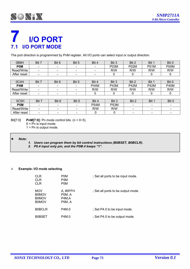
SN8P2711A 8-Bit Micro-Controller
SONiX TECHNOLOGY CO., LTD Page 73 Version 0.1
777 I/O PORT 7.1 I/O PORT MODE The port direction is programmed by PnM register. All I/O ports can select input or output direction.
0B8H Bit 7 Bit 6 Bit 5 Bit 4 Bit 3 Bit 2 Bit 1 Bit 0 P0M - - - - P03M P02M P01M P00M
Read/Write - - - - R/W R/W R/W R/W After reset - - - - 0 0 0 0
0C4H Bit 7 Bit 6 Bit 5 Bit 4 Bit 3 Bit 2 Bit 1 Bit 0 P4M - - - P44M P43M P42M P42M P40M
Read/Write - - - R/W R/W R/W R/W R/W After reset - - - 0 0 0 0 0
0C5H Bit 7 Bit 6 Bit 5 Bit 4 Bit 3 Bit 2 Bit 1 Bit 0 P5M - - - P54M P53M - - -
Read/Write - - - R/W R/W - - - After reset - - - 0 0 - - -
Bit[7:0] PnM[7:0]: Pn mode control bits. (n = 0~5). 0 = Pn is input mode.
1 = Pn is output mode.
Note: 1. Users can program them by bit control instructions (B0BSET, B0BCLR). 2. P0.4 input only pin, and the P0M.4 keeps “1”.
Example: I/O mode selecting CLR P0M ; Set all ports to be input mode. CLR P4M CLR P5M MOV A, #0FFH ; Set all ports to be output mode. B0MOV P0M, A B0MOV P4M,A B0MOV P5M, A B0BCLR P4M.0 ; Set P4.0 to be input mode. B0BSET P4M.0 ; Set P4.0 to be output mode.
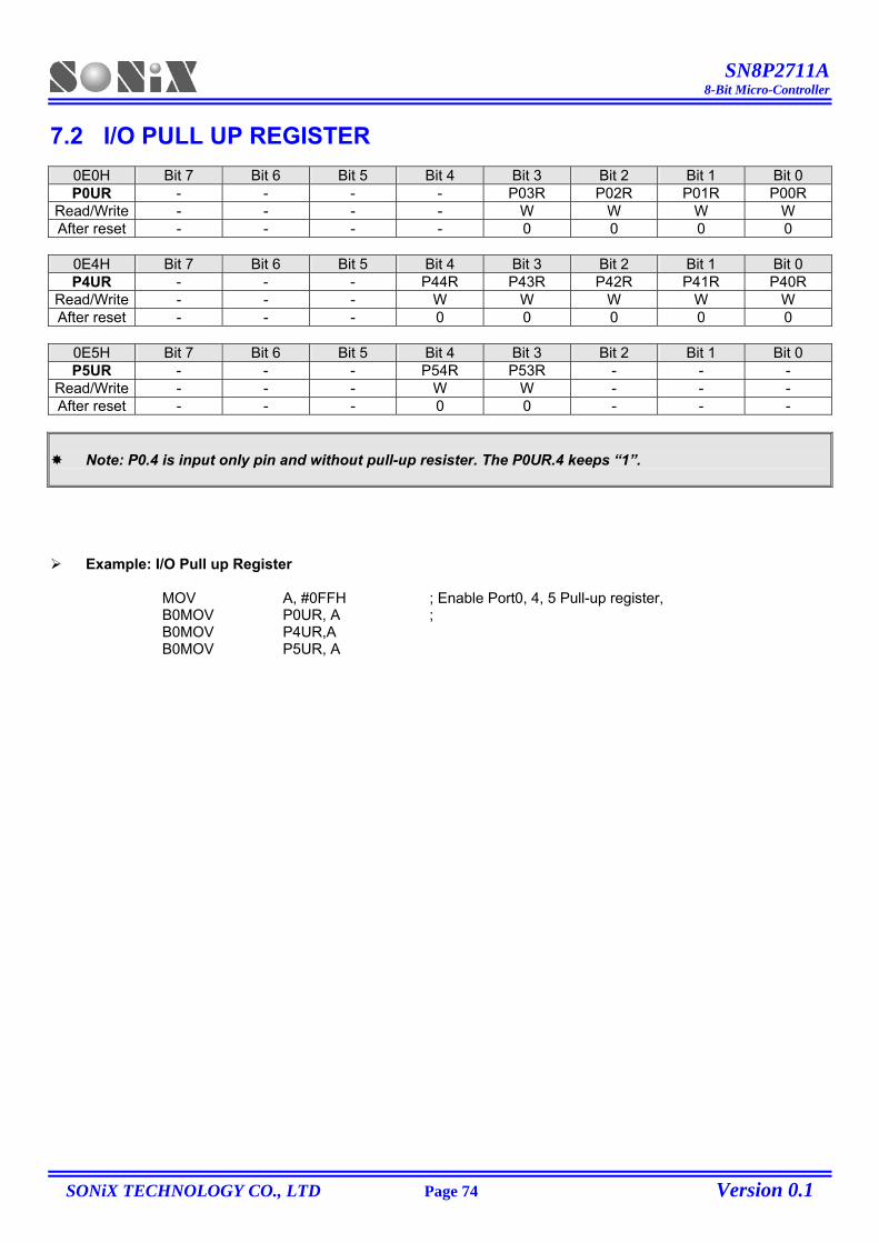
SN8P2711A 8-Bit Micro-Controller
SONiX TECHNOLOGY CO., LTD Page 74 Version 0.1
7.2 I/O PULL UP REGISTER
0E0H Bit 7 Bit 6 Bit 5 Bit 4 Bit 3 Bit 2 Bit 1 Bit 0 P0UR - - - - P03R P02R P01R P00R
Read/Write - - - - W W W W After reset - - - - 0 0 0 0
0E4H Bit 7 Bit 6 Bit 5 Bit 4 Bit 3 Bit 2 Bit 1 Bit 0 P4UR - - - P44R P43R P42R P41R P40R
Read/Write - - - W W W W W After reset - - - 0 0 0 0 0
0E5H Bit 7 Bit 6 Bit 5 Bit 4 Bit 3 Bit 2 Bit 1 Bit 0 P5UR - - - P54R P53R - - -
Read/Write - - - W W - - - After reset - - - 0 0 - - -
Note: P0.4 is input only pin and without pull-up resister. The P0UR.4 keeps “1”.
Example: I/O Pull up Register MOV A, #0FFH ; Enable Port0, 4, 5 Pull-up register, B0MOV P0UR, A ; B0MOV P4UR,A B0MOV P5UR, A
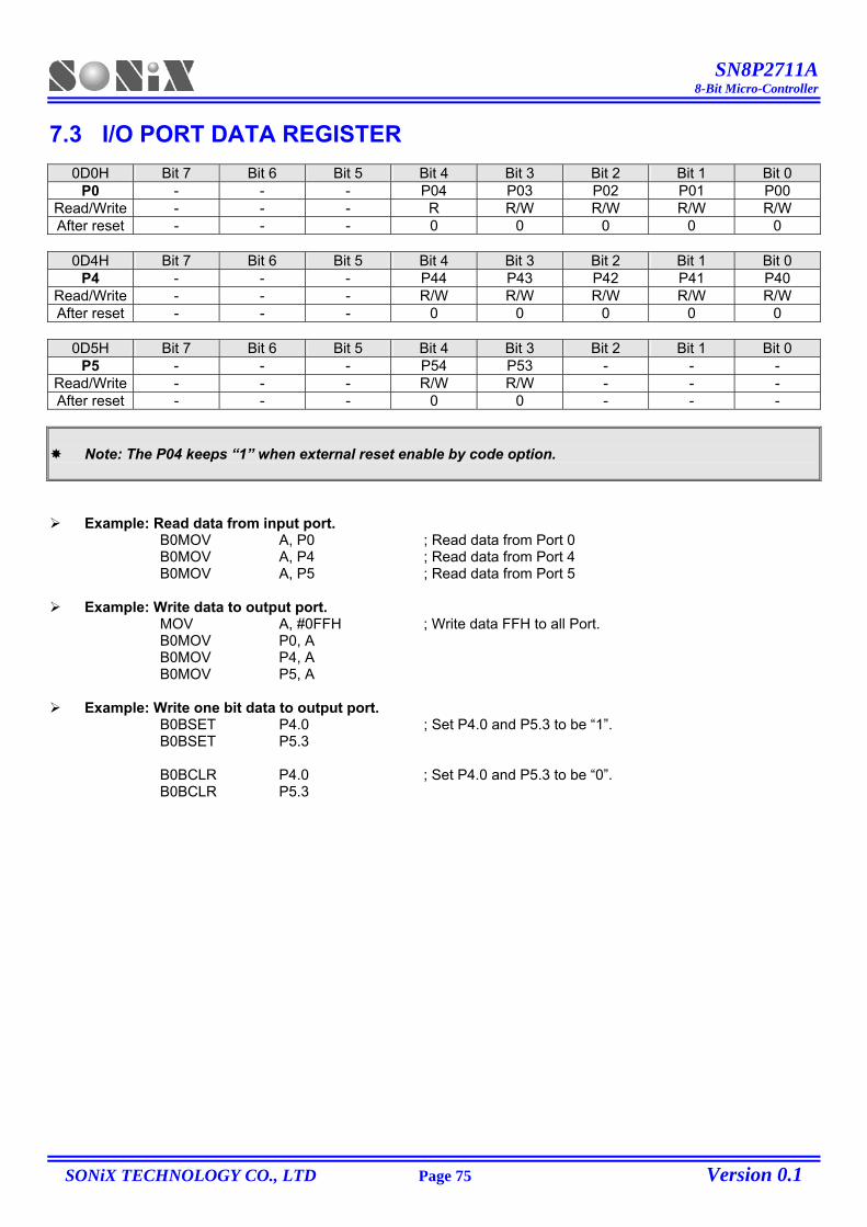
SN8P2711A 8-Bit Micro-Controller
SONiX TECHNOLOGY CO., LTD Page 75 Version 0.1
7.3 I/O PORT DATA REGISTER
0D0H Bit 7 Bit 6 Bit 5 Bit 4 Bit 3 Bit 2 Bit 1 Bit 0 P0 - - - P04 P03 P02 P01 P00
Read/Write - - - R R/W R/W R/W R/W After reset - - - 0 0 0 0 0
0D4H Bit 7 Bit 6 Bit 5 Bit 4 Bit 3 Bit 2 Bit 1 Bit 0
P4 - - - P44 P43 P42 P41 P40 Read/Write - - - R/W R/W R/W R/W R/W After reset - - - 0 0 0 0 0
0D5H Bit 7 Bit 6 Bit 5 Bit 4 Bit 3 Bit 2 Bit 1 Bit 0
P5 - - - P54 P53 - - - Read/Write - - - R/W R/W - - - After reset - - - 0 0 - - -
Note: The P04 keeps “1” when external reset enable by code option.
Example: Read data from input port. B0MOV A, P0 ; Read data from Port 0 B0MOV A, P4 ; Read data from Port 4 B0MOV A, P5 ; Read data from Port 5
Example: Write data to output port. MOV A, #0FFH ; Write data FFH to all Port. B0MOV P0, A B0MOV P4, A B0MOV P5, A
Example: Write one bit data to output port. B0BSET P4.0 ; Set P4.0 and P5.3 to be “1”. B0BSET P5.3 B0BCLR P4.0 ; Set P4.0 and P5.3 to be “0”. B0BCLR P5.3
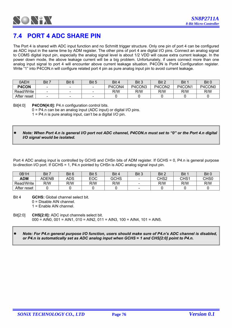
SN8P2711A 8-Bit Micro-Controller
SONiX TECHNOLOGY CO., LTD Page 76 Version 0.1
7.4 PORT 4 ADC SHARE PIN The Port 4 is shared with ADC input function and no Schmitt trigger structure. Only one pin of port 4 can be configured as ADC input in the same time by ADM register. The other pins of port 4 are digital I/O pins. Connect an analog signal to COMS digital input pin, especially the analog signal level is about 1/2 VDD will cause extra current leakage. In the power down mode, the above leakage current will be a big problem. Unfortunately, if users connect more than one analog input signal to port 4 will encounter above current leakage situation. P4CON is Port4 Configuration register. Write “1” into P4CON.n will configure related port 4 pin as pure analog input pin to avoid current leakage.
0AEH Bit 7 Bit 6 Bit 5 Bit 4 Bit 3 Bit 2 Bit 1 Bit 0 P4CON - - - P4CON4 P4CON3 P4CON2 P4CON1 P4CON0
Read/Write - - - R/W R/W R/W R/W R/W After reset - - - 0 0 0 0 0
Bit[4:0] P4CON[4:0]: P4.n configuration control bits. 0 = P4.n can be an analog input (ADC input) or digital I/O pins. 1 = P4.n is pure analog input, can’t be a digital I/O pin.
Note: When Port 4.n is general I/O port not ADC channel, P4CON.n must set to “0” or the Port 4.n digital I/O signal would be isolated.
Port 4 ADC analog input is controlled by GCHS and CHSn bits of ADM register. If GCHS = 0, P4.n is general purpose bi-direction I/O port. If GCHS = 1, P4.n pointed by CHSn is ADC analog signal input pin.
0B1H Bit 7 Bit 6 Bit 5 Bit 4 Bit 3 Bit 2 Bit 1 Bit 0 ADM ADENB ADS EOC GCHS - CHS2 CHS1 CHS0
Read/Write R/W R/W R/W R/W - R/W R/W R/W After reset 0 0 0 0 - 0 0 0
Bit 4 GCHS: Global channel select bit. 0 = Disable AIN channel. 1 = Enable AIN channel. Bit[2:0] CHS[2:0]: ADC input channels select bit. 000 = AIN0, 001 = AIN1, 010 = AIN2, 011 = AIN3, 100 = AIN4, 101 = AIN5.
Note: For P4.n general purpose I/O function, users should make sure of P4.n’s ADC channel is disabled, or P4.n is automatically set as ADC analog input when GCHS = 1 and CHS[2:0] point to P4.n.
SN8P2711A 8-Bit Micro-Controller
SONiX TECHNOLOGY CO., LTD Page 77 Version 0.1
Example: Set P4.1 to be general purpose input mode. P4CON.1 must be set as “0”.
; Check GCHS and CHS[2:0] status. B0BCLR FGCHS ;If CHS[2:0] point to P4.1 (CHS[2:0] = 001B), set GCHS=0 ;If CHS[2:0] don’t point to P4.1 (CHS[2:0] ≠ 001B), don’t
care GCHS status. ; Clear P4CON. B0BCLR P4CON.1 ; Enable P4.1 digital function. ; Enable P4.1 input mode. B0BCLR P4M.1 ; Set P4.1 as input mode.
Example: Set P4.1 to be general purpose output. P4CON.1 must be set as “0”. ; Check GCHS and CHS[2:0] status. B0BCLR FGCHS ;If CHS[2:0] point to P4.1 (CHS[2:0] = 001B), set GCHS=0. ;If CHS[2:0] don’t point to P4.1 (CHS[2:0] ≠ 001B), don’t
care GCHS status. ; Clear P4CON. B0BCLR P4CON.1 ; Enable P4.1 digital function. ; Set P4.1 output buffer to avoid glitch. B0BSET P4.1 ; Set P4.1 buffer as “1”. ; or B0BCLR P4.1 ; Set P4.1 buffer as “0”. ; Enable P4.1 output mode. B0BSET P4M.1 ; Set P4.1 as input mode.
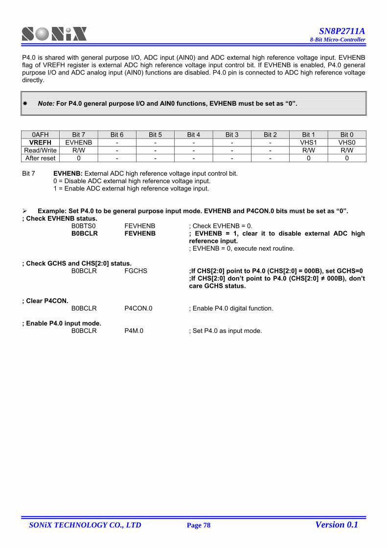
SN8P2711A 8-Bit Micro-Controller
SONiX TECHNOLOGY CO., LTD Page 78 Version 0.1
P4.0 is shared with general purpose I/O, ADC input (AIN0) and ADC external high reference voltage input. EVHENB flag of VREFH register is external ADC high reference voltage input control bit. If EVHENB is enabled, P4.0 general purpose I/O and ADC analog input (AIN0) functions are disabled. P4.0 pin is connected to ADC high reference voltage directly.
Note: For P4.0 general purpose I/O and AIN0 functions, EVHENB must be set as “0”.
0AFH Bit 7 Bit 6 Bit 5 Bit 4 Bit 3 Bit 2 Bit 1 Bit 0 VREFH EVHENB - - - - - VHS1 VHS0
Read/Write R/W - - - - - R/W R/W After reset 0 - - - - - 0 0
Bit 7 EVHENB: External ADC high reference voltage input control bit. 0 = Disable ADC external high reference voltage input. 1 = Enable ADC external high reference voltage input.
Example: Set P4.0 to be general purpose input mode. EVHENB and P4CON.0 bits must be set as “0”. ; Check EVHENB status. B0BTS0 FEVHENB ; Check EVHENB = 0. B0BCLR FEVHENB ; EVHENB = 1, clear it to disable external ADC high
reference input. ; EVHENB = 0, execute next routine. ; Check GCHS and CHS[2:0] status. B0BCLR FGCHS ;If CHS[2:0] point to P4.0 (CHS[2:0] = 000B), set GCHS=0 ;If CHS[2:0] don’t point to P4.0 (CHS[2:0] ≠ 000B), don’t
care GCHS status. ; Clear P4CON. B0BCLR P4CON.0 ; Enable P4.0 digital function. ; Enable P4.0 input mode. B0BCLR P4M.0 ; Set P4.0 as input mode.
SN8P2711A 8-Bit Micro-Controller
SONiX TECHNOLOGY CO., LTD Page 79 Version 0.1
Example: Set P4.0 to be general purpose output. EVHENB and P4CON.0 bits must be set as “0”.
; Check EVHENB status. B0BTS0 FEVHENB ; Check EVHENB = 0. B0BCLR FEVHENB ; EVHENB = 1, clear it to disable external ADC high
reference input. ; EVHENB = 0, execute next routine. ; Check GCHS and CHS[2:0] status. B0BCLR FGCHS ;If CHS[2:0] point to P4.0 (CHS[2:0] = 000B), set GCHS=0 ;If CHS[2:0] don’t point to P4.0 (CHS[2:0] ≠ 000B), don’t
care GCHS status. ; Clear P4CON. B0BCLR P4CON.0 ; Enable P4.0 digital function. ; Set P4.0 output buffer to avoid glitch. B0BSET P4.0 ; Set P4.0 buffer as “1”. ; or B0BCLR P4.0 ; Set P4.0 buffer as “0”. ; Enable P4.0 output mode. B0BSET P4M.0 ; Set P4.0 as input mode.
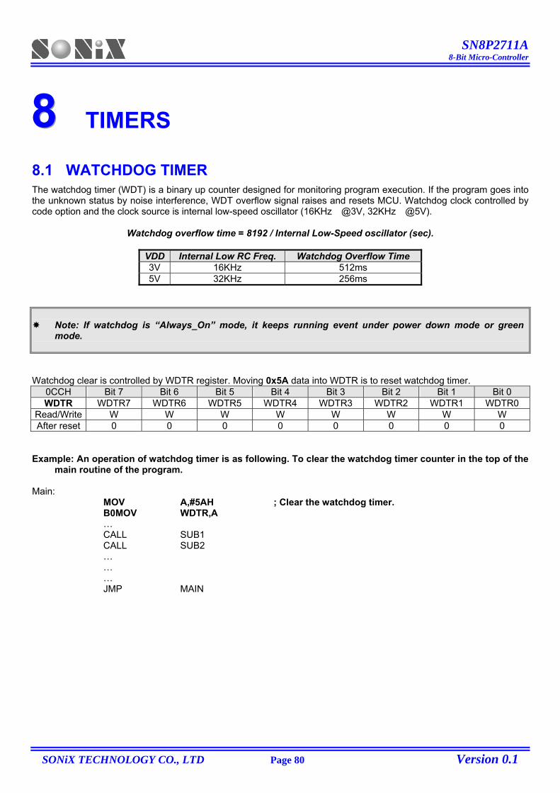
SN8P2711A 8-Bit Micro-Controller
SONiX TECHNOLOGY CO., LTD Page 80 Version 0.1
888 TIMERS
8.1 WATCHDOG TIMER The watchdog timer (WDT) is a binary up counter designed for monitoring program execution. If the program goes into the unknown status by noise interference, WDT overflow signal raises and resets MCU. Watchdog clock controlled by code option and the clock source is internal low-speed oscillator (16KHz @3V, 32KHz @5V).
Watchdog overflow time = 8192 / Internal Low-Speed oscillator (sec).
VDD Internal Low RC Freq. Watchdog Overflow Time 3V 16KHz 512ms 5V 32KHz 256ms
Note: If watchdog is “Always_On” mode, it keeps running event under power down mode or green mode.
Watchdog clear is controlled by WDTR register. Moving 0x5A data into WDTR is to reset watchdog timer.
0CCH Bit 7 Bit 6 Bit 5 Bit 4 Bit 3 Bit 2 Bit 1 Bit 0 WDTR WDTR7 WDTR6 WDTR5 WDTR4 WDTR3 WDTR2 WDTR1 WDTR0
Read/Write W W W W W W W W After reset 0 0 0 0 0 0 0 0
Example: An operation of watchdog timer is as following. To clear the watchdog timer counter in the top of the
main routine of the program. Main: MOV A,#5AH ; Clear the watchdog timer. B0MOV WDTR,A … CALL SUB1 CALL SUB2 … … … JMP MAIN
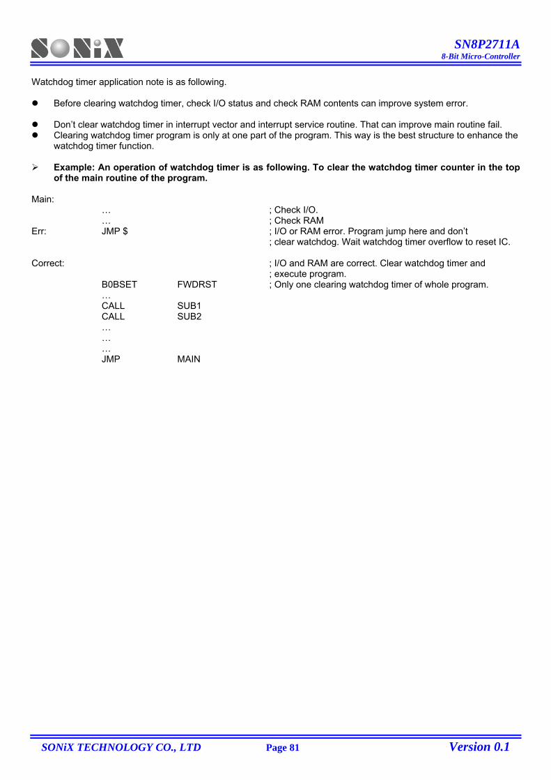
SN8P2711A 8-Bit Micro-Controller
SONiX TECHNOLOGY CO., LTD Page 81 Version 0.1
Watchdog timer application note is as following.
Before clearing watchdog timer, check I/O status and check RAM contents can improve system error.
Don’t clear watchdog timer in interrupt vector and interrupt service routine. That can improve main routine fail. Clearing watchdog timer program is only at one part of the program. This way is the best structure to enhance the
watchdog timer function.
Example: An operation of watchdog timer is as following. To clear the watchdog timer counter in the top of the main routine of the program.
Main: … ; Check I/O. … ; Check RAM Err: JMP $ ; I/O or RAM error. Program jump here and don’t ; clear watchdog. Wait watchdog timer overflow to reset IC. Correct: ; I/O and RAM are correct. Clear watchdog timer and ; execute program. B0BSET FWDRST ; Only one clearing watchdog timer of whole program. … CALL SUB1 CALL SUB2 … … … JMP MAIN

SN8P2711A 8-Bit Micro-Controller
SONiX TECHNOLOGY CO., LTD Page 82 Version 0.1
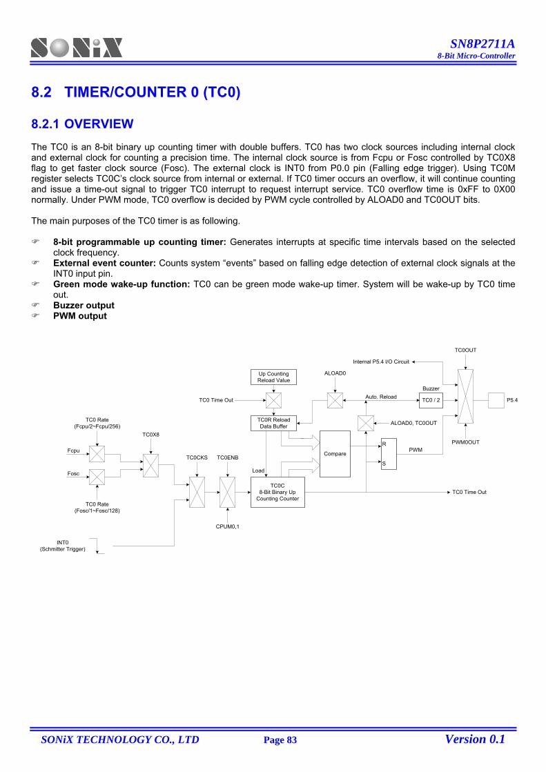
SN8P2711A 8-Bit Micro-Controller
SONiX TECHNOLOGY CO., LTD Page 83 Version 0.1
8.2 TIMER/COUNTER 0 (TC0) 8.2.1 OVERVIEW The TC0 is an 8-bit binary up counting timer with double buffers. TC0 has two clock sources including internal clock and external clock for counting a precision time. The internal clock source is from Fcpu or Fosc controlled by TC0X8 flag to get faster clock source (Fosc). The external clock is INT0 from P0.0 pin (Falling edge trigger). Using TC0M register selects TC0C’s clock source from internal or external. If TC0 timer occurs an overflow, it will continue counting and issue a time-out signal to trigger TC0 interrupt to request interrupt service. TC0 overflow time is 0xFF to 0X00 normally. Under PWM mode, TC0 overflow is decided by PWM cycle controlled by ALOAD0 and TC0OUT bits. The main purposes of the TC0 timer is as following.
8-bit programmable up counting timer: Generates interrupts at specific time intervals based on the selected clock frequency.
External event counter: Counts system “events” based on falling edge detection of external clock signals at the INT0 input pin.
Green mode wake-up function: TC0 can be green mode wake-up timer. System will be wake-up by TC0 time out.
Buzzer output PWM output
Fcpu
TC0 Rate(Fcpu/2~Fcpu/256)
Fosc
TC0 Rate(Fosc/1~Fosc/128)
TC0X8
INT0(Schmitter Trigger)
TC0CKS TC0ENB
CPUM0,1
TC0C8-Bit Binary Up
Counting Counter
TC0R ReloadData Buffer
Up CountingReload Value
TC0 Time Out
Compare
ALOAD0
R
S
TC0 Time Out
Auto. Reload TC0 / 2
Buzzer
Internal P5.4 I/O Circuit
P5.4
PWMPWM0OUT
TC0OUT
ALOAD0, TC0OUT
Load
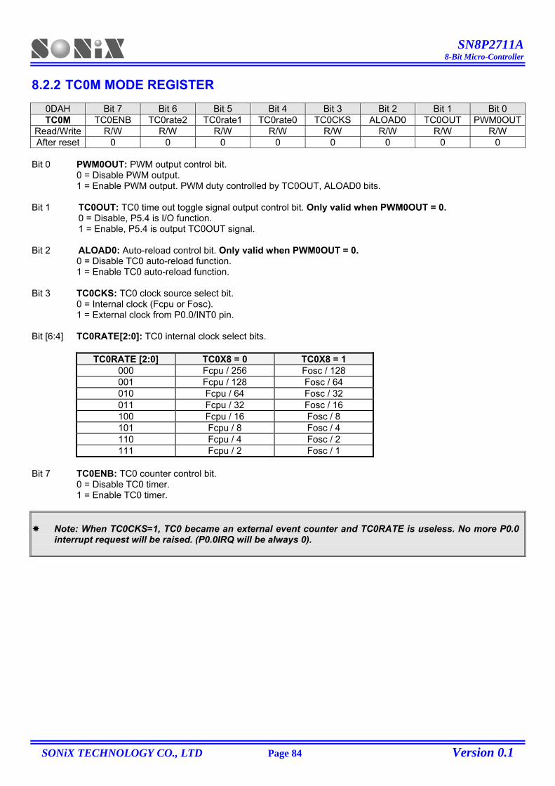
SN8P2711A 8-Bit Micro-Controller
SONiX TECHNOLOGY CO., LTD Page 84 Version 0.1
8.2.2 TC0M MODE REGISTER
0DAH Bit 7 Bit 6 Bit 5 Bit 4 Bit 3 Bit 2 Bit 1 Bit 0 TC0M TC0ENB TC0rate2 TC0rate1 TC0rate0 TC0CKS ALOAD0 TC0OUT PWM0OUT
Read/Write R/W R/W R/W R/W R/W R/W R/W R/W After reset 0 0 0 0 0 0 0 0
Bit 0 PWM0OUT: PWM output control bit.
0 = Disable PWM output. 1 = Enable PWM output. PWM duty controlled by TC0OUT, ALOAD0 bits.
Bit 1 TC0OUT: TC0 time out toggle signal output control bit. Only valid when PWM0OUT = 0. 0 = Disable, P5.4 is I/O function. 1 = Enable, P5.4 is output TC0OUT signal. Bit 2 ALOAD0: Auto-reload control bit. Only valid when PWM0OUT = 0.
0 = Disable TC0 auto-reload function. 1 = Enable TC0 auto-reload function.
Bit 3 TC0CKS: TC0 clock source select bit. 0 = Internal clock (Fcpu or Fosc). 1 = External clock from P0.0/INT0 pin.
Bit [6:4] TC0RATE[2:0]: TC0 internal clock select bits.
TC0RATE [2:0] TC0X8 = 0 TC0X8 = 1 000 Fcpu / 256 Fosc / 128 001 Fcpu / 128 Fosc / 64 010 Fcpu / 64 Fosc / 32 011 Fcpu / 32 Fosc / 16 100 Fcpu / 16 Fosc / 8 101 Fcpu / 8 Fosc / 4 110 Fcpu / 4 Fosc / 2 111 Fcpu / 2 Fosc / 1
Bit 7 TC0ENB: TC0 counter control bit.
0 = Disable TC0 timer. 1 = Enable TC0 timer.
Note: When TC0CKS=1, TC0 became an external event counter and TC0RATE is useless. No more P0.0 interrupt request will be raised. (P0.0IRQ will be always 0).
SN8P2711A 8-Bit Micro-Controller
SONiX TECHNOLOGY CO., LTD Page 85 Version 0.1
8.2.3 TC1X8, TC0X8, TC0GN FLAGS
0D8H Bit 7 Bit 6 Bit 5 Bit 4 Bit 3 Bit 2 Bit 1 Bit 0 T0M - - - - TC1X8 TC0X8 TC0GN -
Read/Write - - - - R/W R/W R/W - After reset - - - - 0 0 0 -
Bit 1 TC0GN: TC0 green mode wake-up function control bit.
0 = Disable TC0 green mode wake-up function. 1 = Enable TC0 green mode wake-up function.
Bit 2 TC0X8: TC0 internal clock source control bit.
0 = TC0 internal clock source is Fcpu. TC0RATE is from Fcpu/2~Fcpu/256. 1 = TC0 internal clock source is Fosc. TC0RATE is from Fosc/1~Fosc/128.
Bit 3 TC1X8: TC1 internal clock source control bit.
0 = TC1 internal clock source is Fcpu. TC1RATE is from Fcpu/2~Fcpu/256. 1 = TC1 internal clock source is Fosc. TC1RATE is from Fosc/1~Fosc/128.
Note: Under TC0 event counter mode (TC0CKS=1), TC0X8 bit and TC0RATE are useless.
8.2.4 TC0C COUNTING REGISTER TC0C is an 8-bit counter register for TC0 interval time control.
0DBH Bit 7 Bit 6 Bit 5 Bit 4 Bit 3 Bit 2 Bit 1 Bit 0 TC0C TC0C7 TC0C6 TC0C5 TC0C4 TC0C3 TC0C2 TC0C1 TC0C0
Read/Write R/W R/W R/W R/W R/W R/W R/W R/W After reset 0 0 0 0 0 0 0 0
The equation of TC0C initial value is as following.
TC0C initial value = N - (TC0 interrupt interval time * input clock) N is TC0 overflow boundary number. TC0 timer overflow time has six types (TC0 timer, TC0 event counter, TC0 Fcpu clock source, TC0 Fosc clock source, PWM mode and no PWM mode). These parameters decide TC0 overflow time and valid value as follow table.
TC0CKS TC0X8 PWM0 ALOAD0 TC0OUT N TC0C valid value
TC0C value binary type Remark
0 x x 256 0x00~0xFF 00000000b~11111111b Overflow per 256 count1 0 0 256 0x00~0xFF 00000000b~11111111b Overflow per 256 count1 0 1 64 0x00~0x3F xx000000b~xx111111b Overflow per 64 count1 1 0 32 0x00~0x1F xxx00000b~xxx11111b Overflow per 32 count
0
(Fcpu/2~ Fcpu/256)
1 1 1 16 0x00~0x0F xxxx0000b~xxxx1111b Overflow per 16 count0 x x 256 0x00~0xFF 00000000b~11111111b Overflow per 256 count1 0 0 256 0x00~0xFF 00000000b~11111111b Overflow per 256 count1 0 1 64 0x00~0x3F xx000000b~xx111111b Overflow per 64 count1 1 0 32 0x00~0x1F xxx00000b~xxx11111b Overflow per 32 count
0
1 (Fosc/1~ Fosc/128)
1 1 1 16 0x00~0x0F xxxx0000b~xxxx1111b Overflow per 16 count1 - - - - 256 0x00~0xFF 00000000b~11111111b Overflow per 256 count
SN8P2711A 8-Bit Micro-Controller
SONiX TECHNOLOGY CO., LTD Page 86 Version 0.1
Example: To set 10ms interval time for TC0 interrupt. TC0 clock source is Fcpu (TC0KS=0, TC0X8=0) and
no PWM output (PWM0=0). High clock is external 4MHz. Fcpu=Fosc/4. Select TC0RATE=010 (Fcpu/64).
TC0C initial value = N - (TC0 interrupt interval time * input clock) = 256 - (10ms * 4MHz / 4 / 64) = 256 - (10-2 * 4 * 106 / 4 / 64) = 100 = 64H
The basic timer table interval time of TC0, TC0X8 = 0.
High speed mode (Fcpu = 4MHz / 4) Low speed mode (Fcpu = 32768Hz / 4) TC0RATE TC0CLOCK Max overflow interval One step = max/256 Max overflow interval One step = max/256
000 Fcpu/256 65.536 ms 256 us 8000 ms 31250 us 001 Fcpu/128 32.768 ms 128 us 4000 ms 15625 us 010 Fcpu/64 16.384 ms 64 us 2000 ms 7812.5 us 011 Fcpu/32 8.192 ms 32 us 1000 ms 3906.25 us 100 Fcpu/16 4.096 ms 16 us 500 ms 1953.125 us 101 Fcpu/8 2.048 ms 8 us 250 ms 976.563 us 110 Fcpu/4 1.024 ms 4 us 125 ms 488.281 us 111 Fcpu/2 0.512 ms 2 us 62.5 ms 244.141 us
The basic timer table interval time of TC0, TC0X8 = 1.
High speed mode (Fcpu = 4MHz / 4) Low speed mode (Fcpu = 32768Hz / 4) TC0RATE TC0CLOCK Max overflow interval One step = max/256 Max overflow interval One step = max/256
000 Fosc/128 8.192 ms 32 us 1000 ms 7812.5 us 001 Fosc/64 4.096 ms 16 us 500 ms 3906.25 us 010 Fosc/32 2.048 ms 8 us 250 ms 1953.125 us 011 Fosc/16 1.024 ms 4 us 125 ms 976.563 us 100 Fosc/8 0.512 ms 2 us 62.5 ms 488.281 us 101 Fosc/4 0.256 ms 1 us 31.25 ms 244.141 us 110 Fosc/2 0.128 ms 0.5 us 15.625 ms 122.07 us 111 Fosc/1 0.064 ms 0.25 us 7.813 ms 61.035 us
SN8P2711A 8-Bit Micro-Controller
SONiX TECHNOLOGY CO., LTD Page 87 Version 0.1
8.2.5 TC0R AUTO-LOAD REGISTER TC0 timer is with auto-load function controlled by ALOAD0 bit of TC0M. When TC0C overflow occurring, TC0R value will load to TC0C by system. It is easy to generate an accurate time, and users don’t reset TC0C during interrupt service routine. TC0 is double buffer design. If new TC0R value is set by program, the new value is stored in 1st buffer. Until TC0 overflow occurs, the new value moves to real TC0R buffer. This way can avoid TC0 interval time error and glitch in PWM and Buzzer output.
Note: Under PWM mode, auto-load is enabled automatically. The ALOAD0 bit is selecting overflow boundary.
0CDH Bit 7 Bit 6 Bit 5 Bit 4 Bit 3 Bit 2 Bit 1 Bit 0 TC0R TC0R7 TC0R6 TC0R5 TC0R4 TC0R3 TC0R2 TC0R1 TC0R0
Read/Write W W W W W W W W After reset 0 0 0 0 0 0 0 0
The equation of TC0R initial value is as following.
TC0R initial value = N - (TC0 interrupt interval time * input clock) N is TC0 overflow boundary number. TC0 timer overflow time has six types (TC0 timer, TC0 event counter, TC0 Fcpu clock source, TC0 Fosc clock source, PWM mode and no PWM mode). These parameters decide TC0 overflow time and valid value as follow table.
TC0CKS TC0X8 PWM0 ALOAD0 TC0OUT N TC0R valid value
TC0R value binary type
0 x x 256 0x00~0xFF 00000000b~11111111b1 0 0 256 0x00~0xFF 00000000b~11111111b1 0 1 64 0x00~0x3F xx000000b~xx111111b 1 1 0 32 0x00~0x1F xxx00000b~xxx11111b
0
(Fcpu/2~ Fcpu/256)
1 1 1 16 0x00~0x0F xxxx0000b~xxxx1111b 0 x x 256 0x00~0xFF 00000000b~11111111b1 0 0 256 0x00~0xFF 00000000b~11111111b1 0 1 64 0x00~0x3F xx000000b~xx111111b 1 1 0 32 0x00~0x1F xxx00000b~xxx11111b
0
1 (Fosc/1~ Fosc/128)
1 1 1 16 0x00~0x0F xxxx0000b~xxxx1111b 1 - - - - 256 0x00~0xFF 00000000b~11111111b
Example: To set 10ms interval time for TC0 interrupt. TC0 clock source is Fcpu (TC0KS=0, TC0X8=0) and no PWM output (PWM0=0). High clock is external 4MHz. Fcpu=Fosc/4. Select TC0RATE=010 (Fcpu/64).
TC0R initial value = N - (TC0 interrupt interval time * input clock) = 256 - (10ms * 4MHz / 4 / 64) = 256 - (10-2 * 4 * 106 / 4 / 64) = 100 = 64H
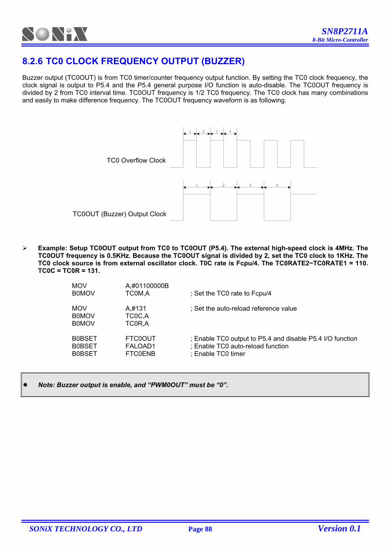
SN8P2711A 8-Bit Micro-Controller
SONiX TECHNOLOGY CO., LTD Page 88 Version 0.1
8.2.6 TC0 CLOCK FREQUENCY OUTPUT (BUZZER) Buzzer output (TC0OUT) is from TC0 timer/counter frequency output function. By setting the TC0 clock frequency, the clock signal is output to P5.4 and the P5.4 general purpose I/O function is auto-disable. The TC0OUT frequency is divided by 2 from TC0 interval time. TC0OUT frequency is 1/2 TC0 frequency. The TC0 clock has many combinations and easily to make difference frequency. The TC0OUT frequency waveform is as following.
1 2 3 4
1 2 3 4
TC0 Overflow Clock
TC0OUT (Buzzer) Output Clock
Example: Setup TC0OUT output from TC0 to TC0OUT (P5.4). The external high-speed clock is 4MHz. The TC0OUT frequency is 0.5KHz. Because the TC0OUT signal is divided by 2, set the TC0 clock to 1KHz. The TC0 clock source is from external oscillator clock. T0C rate is Fcpu/4. The TC0RATE2~TC0RATE1 = 110. TC0C = TC0R = 131.
MOV A,#01100000B B0MOV TC0M,A ; Set the TC0 rate to Fcpu/4 MOV A,#131 ; Set the auto-reload reference value B0MOV TC0C,A B0MOV TC0R,A B0BSET FTC0OUT ; Enable TC0 output to P5.4 and disable P5.4 I/O function B0BSET FALOAD1 ; Enable TC0 auto-reload function B0BSET FTC0ENB ; Enable TC0 timer
Note: Buzzer output is enable, and “PWM0OUT” must be “0”.
SN8P2711A 8-Bit Micro-Controller
SONiX TECHNOLOGY CO., LTD Page 89 Version 0.1
8.2.7 TC0 TIMER OPERATION SEQUENCE TC0 timer operation includes timer interrupt, event counter, TC0OUT and PWM. The sequence of setup TC0 timer is as following.
Stop TC0 timer counting, disable TC0 interrupt function and clear TC0 interrupt request flag. B0BCLR FTC0ENB ; TC0 timer, TC0OUT and PWM stop. B0BCLR FTC0IEN ; TC0 interrupt function is disabled. B0BCLR FTC0IRQ ; TC0 interrupt request flag is cleared.
Set TC0 timer rate. (Besides event counter mode.) MOV A, #0xxx0000b ;The TC0 rate control bits exist in bit4~bit6 of TC0M. The ; value is from x000xxxxb~x111xxxxb. B0MOV TC0M,A ; TC0 interrupt function is disabled.
Set TC0 timer clock source. ; Select TC0 internal / external clock source. B0BCLR FTC0CKS ; Select TC0 internal clock source. or B0BSET FTC0CKS ; Select TC0 external clock source. ; Select TC0 Fcpu / Fosc internal clock source . B0BCLR FTC0X8 ; Select TC0 Fcpu internal clock source. or B0BSET FTC0X8 ; Select TC0 Fosc internal clock source.
Note: TC0X8 is useless in TC0 external clock source mode.
Set TC0 timer auto-load mode.
B0BCLR FALOAD0 ; Enable TC0 auto reload function. or B0BSET FALOAD0 ; Disable TC0 auto reload function.
Set TC0 interrupt interval time, TC0OUT (Buzzer) frequency or PWM duty cycle. ; Set TC0 interrupt interval time, TC0OUT (Buzzer) frequency or PWM duty.
MOV A,#7FH ; TC0C and TC0R value is decided by TC0 mode. B0MOV TC0C,A ; Set TC0C value. B0MOV TC0R,A ; Set TC0R value under auto reload mode or PWM mode.
; In PWM mode, set PWM cycle. B0BCLR FALOAD0 ; ALOAD0, TC0OUT = 00, PWM cycle boundary is B0BCLR FTC0OUT ; 0~255. or B0BCLR FALOAD0 ; ALOAD0, TC0OUT = 01, PWM cycle boundary is B0BSET FTC0OUT ; 0~63. or B0BSET FALOAD0 ; ALOAD0, TC0OUT = 10, PWM cycle boundary is B0BCLR FTC0OUT ; 0~31. or B0BSET FALOAD0 ; ALOAD0, TC0OUT = 11, PWM cycle boundary is B0BSET FTC0OUT ; 0~15.
SN8P2711A 8-Bit Micro-Controller
SONiX TECHNOLOGY CO., LTD Page 90 Version 0.1
Set TC0 timer function mode.
B0BSET FTC0IEN ; Enable TC0 interrupt function. or B0BSET FTC0OUT ; Enable TC0OUT (Buzzer) function. or B0BSET FPWM0OUT ; Enable PWM function. or B0BSET FTC0GN ; Enable TC0 green mode wake-up function.
Enable TC0 timer. B0BSET FTC0ENB ; Enable TC0 timer.
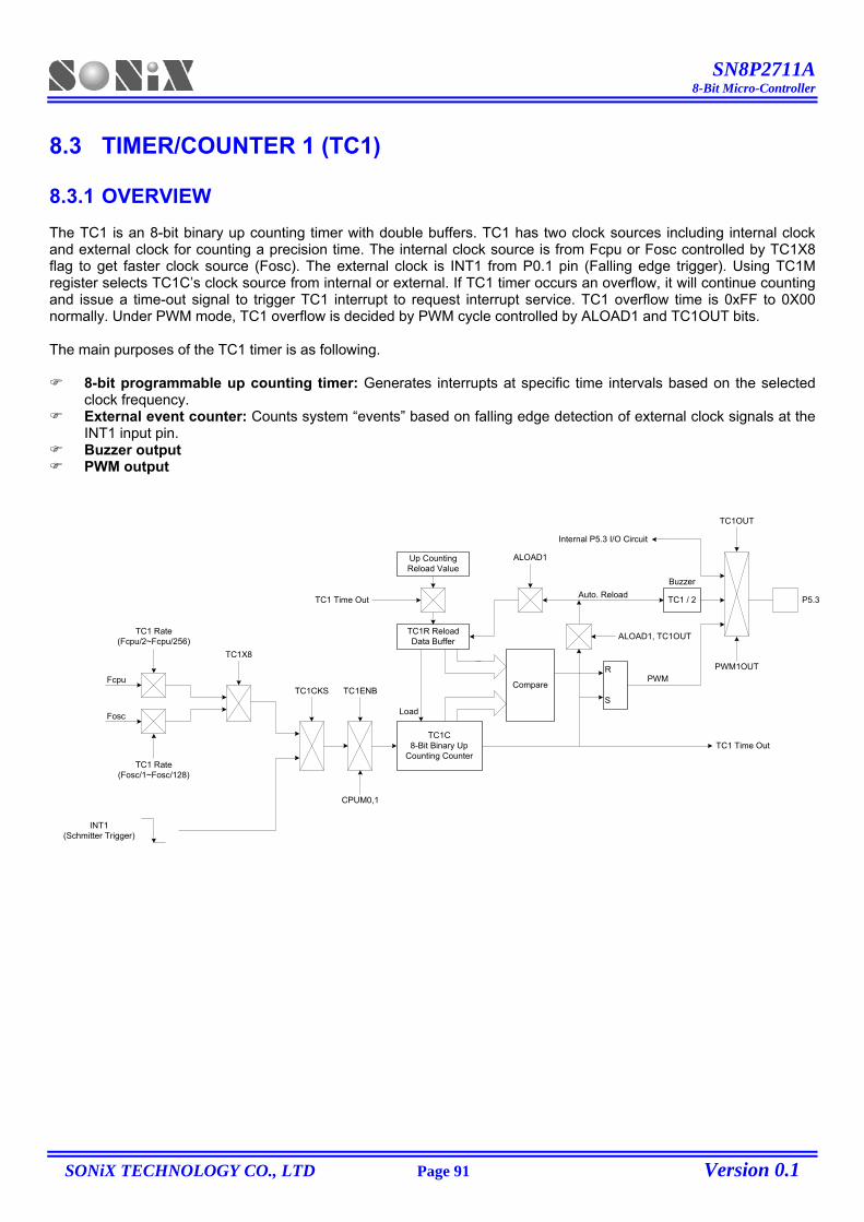
SN8P2711A 8-Bit Micro-Controller
SONiX TECHNOLOGY CO., LTD Page 91 Version 0.1
8.3 TIMER/COUNTER 1 (TC1) 8.3.1 OVERVIEW The TC1 is an 8-bit binary up counting timer with double buffers. TC1 has two clock sources including internal clock and external clock for counting a precision time. The internal clock source is from Fcpu or Fosc controlled by TC1X8 flag to get faster clock source (Fosc). The external clock is INT1 from P0.1 pin (Falling edge trigger). Using TC1M register selects TC1C’s clock source from internal or external. If TC1 timer occurs an overflow, it will continue counting and issue a time-out signal to trigger TC1 interrupt to request interrupt service. TC1 overflow time is 0xFF to 0X00 normally. Under PWM mode, TC1 overflow is decided by PWM cycle controlled by ALOAD1 and TC1OUT bits. The main purposes of the TC1 timer is as following.
8-bit programmable up counting timer: Generates interrupts at specific time intervals based on the selected clock frequency.
External event counter: Counts system “events” based on falling edge detection of external clock signals at the INT1 input pin.
Buzzer output PWM output
Fcpu
TC1 Rate(Fcpu/2~Fcpu/256)
Fosc
TC1 Rate(Fosc/1~Fosc/128)
TC1X8
INT1(Schmitter Trigger)
TC1CKS TC1ENB
CPUM0,1
TC1C8-Bit Binary Up
Counting Counter
TC1R ReloadData Buffer
Up CountingReload Value
TC1 Time Out
Compare
ALOAD1
R
S
TC1 Time Out
Auto. Reload TC1 / 2
Buzzer
Internal P5.3 I/O Circuit
P5.3
PWMPWM1OUT
TC1OUT
ALOAD1, TC1OUT
Load
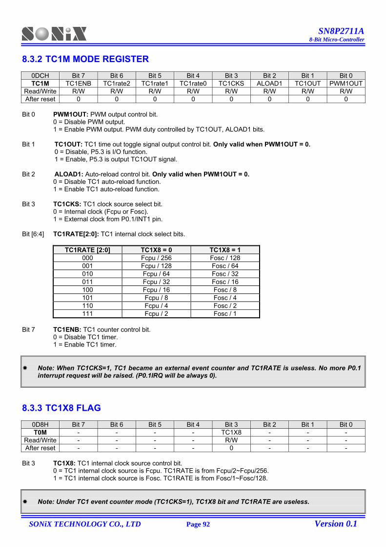
SN8P2711A 8-Bit Micro-Controller
SONiX TECHNOLOGY CO., LTD Page 92 Version 0.1
8.3.2 TC1M MODE REGISTER
0DCH Bit 7 Bit 6 Bit 5 Bit 4 Bit 3 Bit 2 Bit 1 Bit 0 TC1M TC1ENB TC1rate2 TC1rate1 TC1rate0 TC1CKS ALOAD1 TC1OUT PWM1OUT
Read/Write R/W R/W R/W R/W R/W R/W R/W R/W After reset 0 0 0 0 0 0 0 0
Bit 0 PWM1OUT: PWM output control bit.
0 = Disable PWM output. 1 = Enable PWM output. PWM duty controlled by TC1OUT, ALOAD1 bits.
Bit 1 TC1OUT: TC1 time out toggle signal output control bit. Only valid when PWM1OUT = 0. 0 = Disable, P5.3 is I/O function. 1 = Enable, P5.3 is output TC1OUT signal. Bit 2 ALOAD1: Auto-reload control bit. Only valid when PWM1OUT = 0.
0 = Disable TC1 auto-reload function. 1 = Enable TC1 auto-reload function.
Bit 3 TC1CKS: TC1 clock source select bit. 0 = Internal clock (Fcpu or Fosc). 1 = External clock from P0.1/INT1 pin.
Bit [6:4] TC1RATE[2:0]: TC1 internal clock select bits.
TC1RATE [2:0] TC1X8 = 0 TC1X8 = 1 000 Fcpu / 256 Fosc / 128 001 Fcpu / 128 Fosc / 64 010 Fcpu / 64 Fosc / 32 011 Fcpu / 32 Fosc / 16 100 Fcpu / 16 Fosc / 8 101 Fcpu / 8 Fosc / 4 110 Fcpu / 4 Fosc / 2 111 Fcpu / 2 Fosc / 1
Bit 7 TC1ENB: TC1 counter control bit.
0 = Disable TC1 timer. 1 = Enable TC1 timer.
Note: When TC1CKS=1, TC1 became an external event counter and TC1RATE is useless. No more P0.1 interrupt request will be raised. (P0.1IRQ will be always 0).
8.3.3 TC1X8 FLAG
0D8H Bit 7 Bit 6 Bit 5 Bit 4 Bit 3 Bit 2 Bit 1 Bit 0 T0M - - - - TC1X8 - - -
Read/Write - - - - R/W - - - After reset - - - - 0 - - -
Bit 3 TC1X8: TC1 internal clock source control bit.
0 = TC1 internal clock source is Fcpu. TC1RATE is from Fcpu/2~Fcpu/256. 1 = TC1 internal clock source is Fosc. TC1RATE is from Fosc/1~Fosc/128.
Note: Under TC1 event counter mode (TC1CKS=1), TC1X8 bit and TC1RATE are useless.
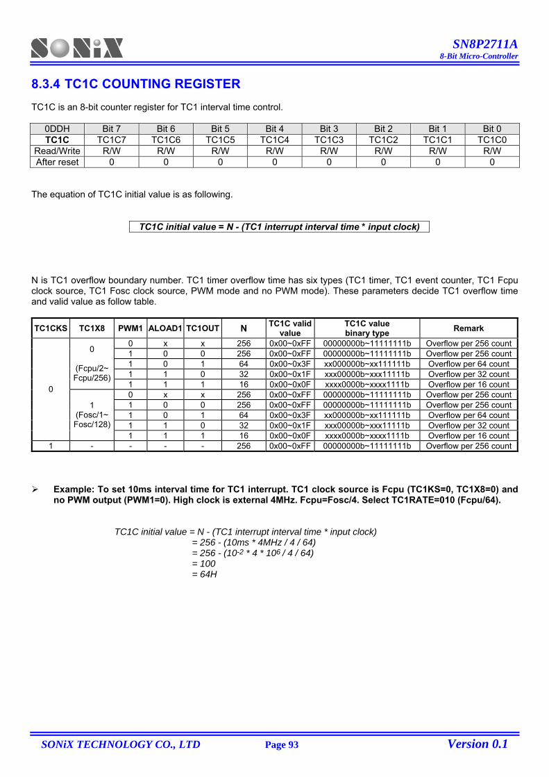
SN8P2711A 8-Bit Micro-Controller
SONiX TECHNOLOGY CO., LTD Page 93 Version 0.1
8.3.4 TC1C COUNTING REGISTER TC1C is an 8-bit counter register for TC1 interval time control.
0DDH Bit 7 Bit 6 Bit 5 Bit 4 Bit 3 Bit 2 Bit 1 Bit 0 TC1C TC1C7 TC1C6 TC1C5 TC1C4 TC1C3 TC1C2 TC1C1 TC1C0
Read/Write R/W R/W R/W R/W R/W R/W R/W R/W After reset 0 0 0 0 0 0 0 0
The equation of TC1C initial value is as following.
TC1C initial value = N - (TC1 interrupt interval time * input clock) N is TC1 overflow boundary number. TC1 timer overflow time has six types (TC1 timer, TC1 event counter, TC1 Fcpu clock source, TC1 Fosc clock source, PWM mode and no PWM mode). These parameters decide TC1 overflow time and valid value as follow table.
TC1CKS TC1X8 PWM1 ALOAD1 TC1OUT N TC1C valid value
TC1C value binary type Remark
0 x x 256 0x00~0xFF 00000000b~11111111b Overflow per 256 count1 0 0 256 0x00~0xFF 00000000b~11111111b Overflow per 256 count1 0 1 64 0x00~0x3F xx000000b~xx111111b Overflow per 64 count1 1 0 32 0x00~0x1F xxx00000b~xxx11111b Overflow per 32 count
0
(Fcpu/2~ Fcpu/256)
1 1 1 16 0x00~0x0F xxxx0000b~xxxx1111b Overflow per 16 count0 x x 256 0x00~0xFF 00000000b~11111111b Overflow per 256 count1 0 0 256 0x00~0xFF 00000000b~11111111b Overflow per 256 count1 0 1 64 0x00~0x3F xx000000b~xx111111b Overflow per 64 count1 1 0 32 0x00~0x1F xxx00000b~xxx11111b Overflow per 32 count
0
1 (Fosc/1~ Fosc/128)
1 1 1 16 0x00~0x0F xxxx0000b~xxxx1111b Overflow per 16 count1 - - - - 256 0x00~0xFF 00000000b~11111111b Overflow per 256 count
Example: To set 10ms interval time for TC1 interrupt. TC1 clock source is Fcpu (TC1KS=0, TC1X8=0) and no PWM output (PWM1=0). High clock is external 4MHz. Fcpu=Fosc/4. Select TC1RATE=010 (Fcpu/64).
TC1C initial value = N - (TC1 interrupt interval time * input clock) = 256 - (10ms * 4MHz / 4 / 64) = 256 - (10-2 * 4 * 106 / 4 / 64) = 100 = 64H
SN8P2711A 8-Bit Micro-Controller
SONiX TECHNOLOGY CO., LTD Page 94 Version 0.1
The basic timer table interval time of TC1, TC1X8 = 0.
High speed mode (Fcpu = 4MHz / 4) Low speed mode (Fcpu = 32768Hz / 4) TC1RATE TC1CLOCK Max overflow interval One step = max/256 Max overflow interval One step = max/256
000 Fcpu/256 65.536 ms 256 us 8000 ms 31250 us 001 Fcpu/128 32.768 ms 128 us 4000 ms 15625 us 010 Fcpu/64 16.384 ms 64 us 2000 ms 7812.5 us 011 Fcpu/32 8.192 ms 32 us 1000 ms 3906.25 us 100 Fcpu/16 4.096 ms 16 us 500 ms 1953.125 us 101 Fcpu/8 2.048 ms 8 us 250 ms 976.563 us 110 Fcpu/4 1.024 ms 4 us 125 ms 488.281 us 111 Fcpu/2 0.512 ms 2 us 62.5 ms 244.141 us
The basic timer table interval time of TC1, TC1X8 = 1.
High speed mode (Fcpu = 4MHz / 4) Low speed mode (Fcpu = 32768Hz / 4) TC1RATE TC1CLOCK Max overflow interval One step = max/256 Max overflow interval One step = max/256
000 Fosc/128 8.192 ms 32 us 1000 ms 7812.5 us 001 Fosc/64 4.096 ms 16 us 500 ms 3906.25 us 010 Fosc/32 2.048 ms 8 us 250 ms 1953.125 us 011 Fosc/16 1.024 ms 4 us 125 ms 976.563 us 100 Fosc/8 0.512 ms 2 us 62.5 ms 488.281 us 101 Fosc/4 0.256 ms 1 us 31.25 ms 244.141 us 110 Fosc/2 0.128 ms 0.5 us 15.625 ms 122.07 us 111 Fosc/1 0.064 ms 0.25 us 7.813 ms 61.035 us
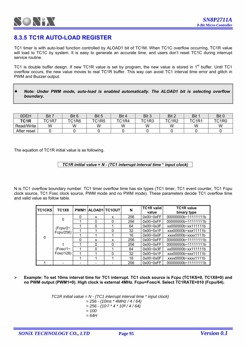
SN8P2711A 8-Bit Micro-Controller
SONiX TECHNOLOGY CO., LTD Page 95 Version 0.1
8.3.5 TC1R AUTO-LOAD REGISTER TC1 timer is with auto-load function controlled by ALOAD1 bit of TC1M. When TC1C overflow occurring, TC1R value will load to TC1C by system. It is easy to generate an accurate time, and users don’t reset TC1C during interrupt service routine. TC1 is double buffer design. If new TC1R value is set by program, the new value is stored in 1st buffer. Until TC1 overflow occurs, the new value moves to real TC1R buffer. This way can avoid TC1 interval time error and glitch in PWM and Buzzer output.
Note: Under PWM mode, auto-load is enabled automatically. The ALOAD1 bit is selecting overflow boundary.
0DEH Bit 7 Bit 6 Bit 5 Bit 4 Bit 3 Bit 2 Bit 1 Bit 0 TC1R TC1R7 TC1R6 TC1R5 TC1R4 TC1R3 TC1R2 TC1R1 TC1R0
Read/Write W W W W W W W W After reset 0 0 0 0 0 0 0 0
The equation of TC1R initial value is as following.
TC1R initial value = N - (TC1 interrupt interval time * input clock) N is TC1 overflow boundary number. TC1 timer overflow time has six types (TC1 timer, TC1 event counter, TC1 Fcpu clock source, TC1 Fosc clock source, PWM mode and no PWM mode). These parameters decide TC1 overflow time and valid value as follow table.
TC1CKS TC1X8 PWM1 ALOAD1 TC1OUT N TC1R valid value
TC1R value binary type
0 x x 256 0x00~0xFF 00000000b~11111111b1 0 0 256 0x00~0xFF 00000000b~11111111b1 0 1 64 0x00~0x3F xx000000b~xx111111b 1 1 0 32 0x00~0x1F xxx00000b~xxx11111b
0
(Fcpu/2~ Fcpu/256)
1 1 1 16 0x00~0x0F xxxx0000b~xxxx1111b 0 x x 256 0x00~0xFF 00000000b~11111111b1 0 0 256 0x00~0xFF 00000000b~11111111b1 0 1 64 0x00~0x3F xx000000b~xx111111b 1 1 0 32 0x00~0x1F xxx00000b~xxx11111b
0
1 (Fosc/1~ Fosc/128)
1 1 1 16 0x00~0x0F xxxx0000b~xxxx1111b 1 - - - - 256 0x00~0xFF 00000000b~11111111b
Example: To set 10ms interval time for TC1 interrupt. TC1 clock source is Fcpu (TC1KS=0, TC1X8=0) and no PWM output (PWM1=0). High clock is external 4MHz. Fcpu=Fosc/4. Select TC1RATE=010 (Fcpu/64).
TC1R initial value = N - (TC1 interrupt interval time * input clock) = 256 - (10ms * 4MHz / 4 / 64) = 256 - (10-2 * 4 * 106 / 4 / 64) = 100 = 64H
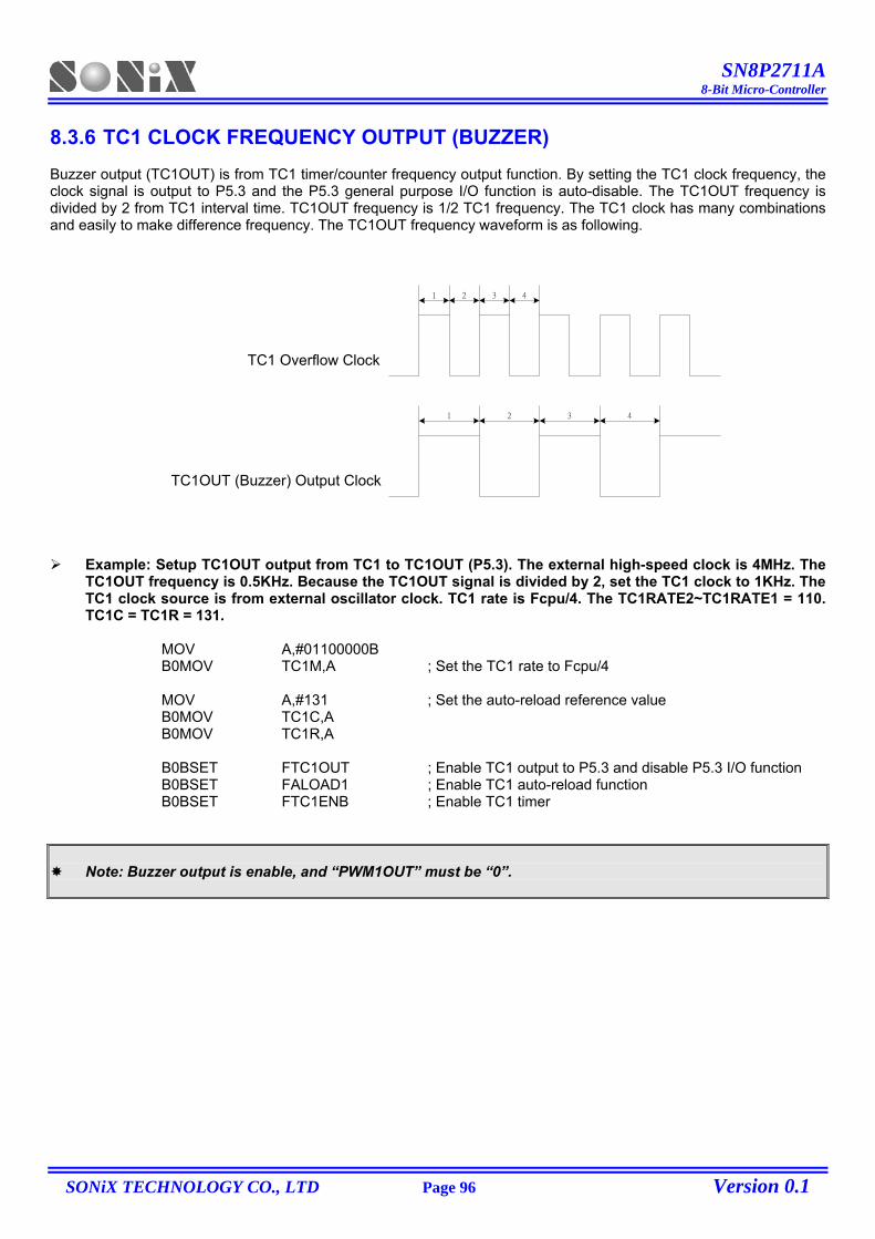
SN8P2711A 8-Bit Micro-Controller
SONiX TECHNOLOGY CO., LTD Page 96 Version 0.1
8.3.6 TC1 CLOCK FREQUENCY OUTPUT (BUZZER) Buzzer output (TC1OUT) is from TC1 timer/counter frequency output function. By setting the TC1 clock frequency, the clock signal is output to P5.3 and the P5.3 general purpose I/O function is auto-disable. The TC1OUT frequency is divided by 2 from TC1 interval time. TC1OUT frequency is 1/2 TC1 frequency. The TC1 clock has many combinations and easily to make difference frequency. The TC1OUT frequency waveform is as following.
1 2 3 4
1 2 3 4
TC1 Overflow Clock
TC1OUT (Buzzer) Output Clock
Example: Setup TC1OUT output from TC1 to TC1OUT (P5.3). The external high-speed clock is 4MHz. The TC1OUT frequency is 0.5KHz. Because the TC1OUT signal is divided by 2, set the TC1 clock to 1KHz. The TC1 clock source is from external oscillator clock. TC1 rate is Fcpu/4. The TC1RATE2~TC1RATE1 = 110. TC1C = TC1R = 131.
MOV A,#01100000B B0MOV TC1M,A ; Set the TC1 rate to Fcpu/4 MOV A,#131 ; Set the auto-reload reference value B0MOV TC1C,A B0MOV TC1R,A B0BSET FTC1OUT ; Enable TC1 output to P5.3 and disable P5.3 I/O function B0BSET FALOAD1 ; Enable TC1 auto-reload function B0BSET FTC1ENB ; Enable TC1 timer
Note: Buzzer output is enable, and “PWM1OUT” must be “0”.
SN8P2711A 8-Bit Micro-Controller
SONiX TECHNOLOGY CO., LTD Page 97 Version 0.1
8.3.7 TC1 TIMER OPERATION SEQUENCE TC1 timer operation includes timer interrupt, event counter, TC1OUT and PWM. The sequence of setup TC1 timer is as following.
Stop TC1 timer counting, disable TC1 interrupt function and clear TC1 interrupt request flag. B0BCLR FTC1ENB ; TC1 timer, TC1OUT and PWM stop. B0BCLR FTC1IEN ; TC1 interrupt function is disabled. B0BCLR FTC1IRQ ; TC1 interrupt request flag is cleared.
Set TC1 timer rate. (Besides event counter mode.) MOV A, #0xxx0000b ;The TC1 rate control bits exist in bit4~bit6 of TC1M. The ; value is from x000xxxxb~x111xxxxb. B0MOV TC1M,A ; TC1 timer is disabled.
Set TC1 timer clock source. ; Select TC1 internal / external clock source. B0BCLR FTC1CKS ; Select TC1 internal clock source. or B0BSET FTC1CKS ; Select TC1 external clock source. ; Select TC1 Fcpu / Fosc internal clock source . B0BCLR FTC1X8 ; Select TC1 Fcpu internal clock source. or B0BSET FTC1X8 ; Select TC1 Fosc internal clock source.
Note: TC1X8 is useless in TC1 external clock source mode.
Set TC1 timer auto-load mode.
B0BCLR FALOAD1 ; Enable TC1 auto reload function. or B0BSET FALOAD1 ; Disable TC1 auto reload function.
Set TC1 interrupt interval time, TC1OUT (Buzzer) frequency or PWM duty cycle. ; Set TC1 interrupt interval time, TC1OUT (Buzzer) frequency or PWM duty.
MOV A,#7FH ; TC1C and TC1R value is decided by TC1 mode. B0MOV TC1C,A ; Set TC1C value. B0MOV TC1R,A ; Set TC1R value under auto reload mode or PWM mode.
; In PWM mode, set PWM cycle. B0BCLR FALOAD1 ; ALOAD1, TC1OUT = 00, PWM cycle boundary is 0~255. B0BCLR FTC1OUT or B0BCLR FALOAD1 ; ALOAD1, TC1OUT = 01, PWM cycle boundary is 0~63. B0BSET FTC1OUT or B0BSET FALOAD1 ; ALOAD1, TC1OUT = 10, PWM cycle boundary is 0~31. B0BCLR FTC1OUT or B0BSET FALOAD1 ; ALOAD1, TC1OUT = 11, PWM cycle boundary is 0~15. B0BSET FTC1OUT
SN8P2711A 8-Bit Micro-Controller
SONiX TECHNOLOGY CO., LTD Page 98 Version 0.1
Set TC1 timer function mode.
B0BSET FTC1IEN ; Enable TC1 interrupt function. or B0BSET FTC1OUT ; Enable TC1OUT (Buzzer) function. or B0BSET FPWM1OUT ; Enable PWM function.
Enable TC1 timer. B0BSET FTC1ENB ; Enable TC1 timer.
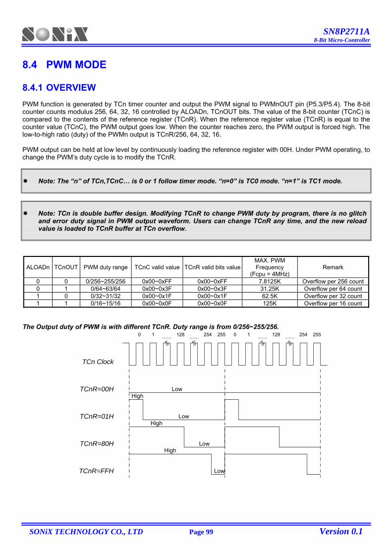
SN8P2711A 8-Bit Micro-Controller
SONiX TECHNOLOGY CO., LTD Page 99 Version 0.1
8.4 PWM MODE 8.4.1 OVERVIEW PWM function is generated by TCn timer counter and output the PWM signal to PWMnOUT pin (P5.3/P5.4). The 8-bit counter counts modulus 256, 64, 32, 16 controlled by ALOADn, TCnOUT bits. The value of the 8-bit counter (TCnC) is compared to the contents of the reference register (TCnR). When the reference register value (TCnR) is equal to the counter value (TCnC), the PWM output goes low. When the counter reaches zero, the PWM output is forced high. The low-to-high ratio (duty) of the PWMn output is TCnR/256, 64, 32, 16. PWM output can be held at low level by continuously loading the reference register with 00H. Under PWM operating, to change the PWM’s duty cycle is to modify the TCnR.
Note: The “n” of TCn,TCnC… is 0 or 1 follow timer mode. “n=0” is TC0 mode. “n=1” is TC1 mode.
Note: TCn is double buffer design. Modifying TCnR to change PWM duty by program, there is no glitch and error duty signal in PWM output waveform. Users can change TCnR any time, and the new reload value is loaded to TCnR buffer at TCn overflow.
ALOADn TCnOUT PWM duty range TCnC valid value TCnR valid bits valueMAX. PWM Frequency
(Fcpu = 4MHz) Remark
0 0 0/256~255/256 0x00~0xFF 0x00~0xFF 7.8125K Overflow per 256 count0 1 0/64~63/64 0x00~0x3F 0x00~0x3F 31.25K Overflow per 64 count 1 0 0/32~31/32 0x00~0x1F 0x00~0x1F 62.5K Overflow per 32 count 1 1 0/16~15/16 0x00~0x0F 0x00~0x0F 125K Overflow per 16 count
The Output duty of PWM is with different TCnR. Duty range is from 0/256~255/256.
TCn Clock
TCnR=00H
TCnR=01H
TCnR=80H
TCnR=FFH
0 1 128 254 255…… ……
0 1 128 254 255…… ……
Low
Low
Low
High
High
Low
High
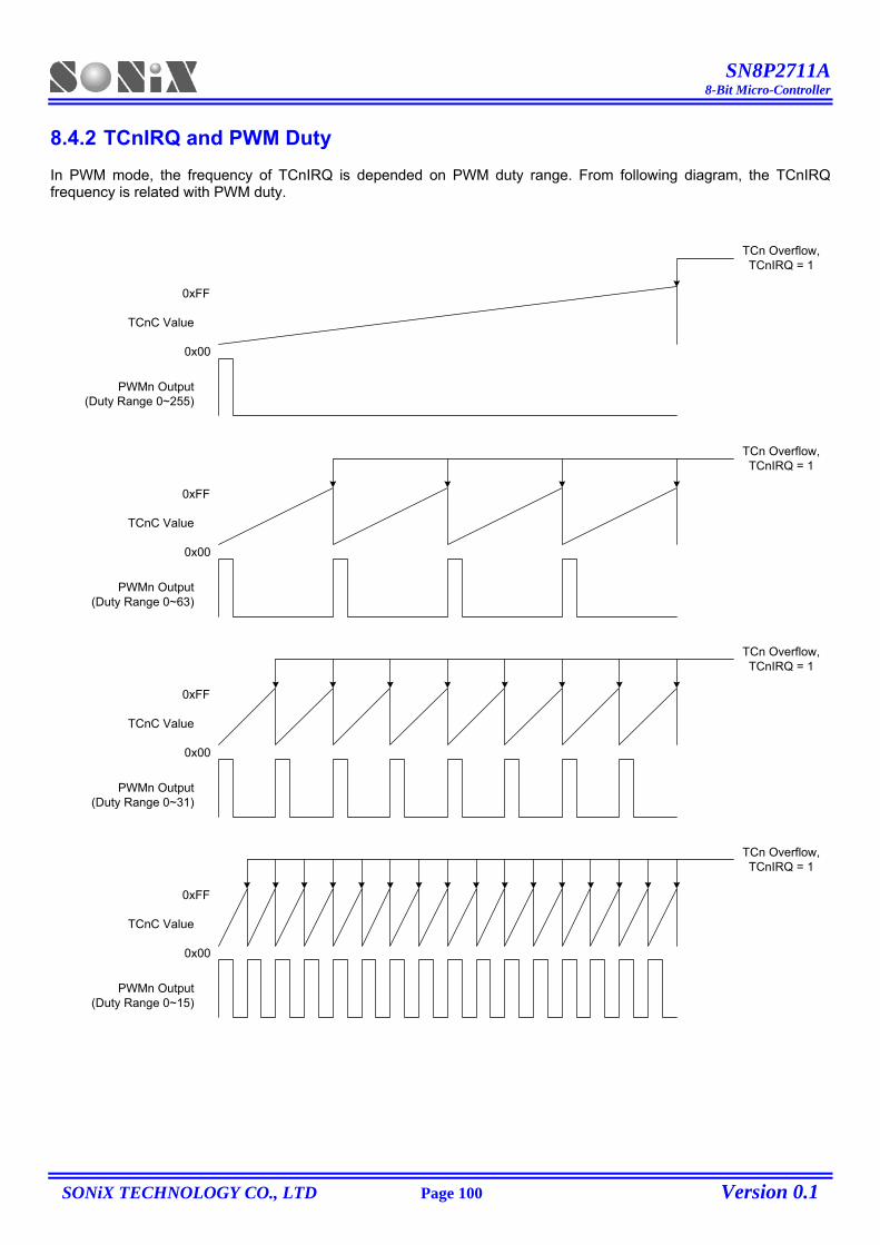
SN8P2711A 8-Bit Micro-Controller
SONiX TECHNOLOGY CO., LTD Page 100 Version 0.1
8.4.2 TCnIRQ and PWM Duty In PWM mode, the frequency of TCnIRQ is depended on PWM duty range. From following diagram, the TCnIRQ frequency is related with PWM duty.
TCn Overflow,TCnIRQ = 1
PWMn Output(Duty Range 0~15)
0xFF
TCnC Value
0x00
PWMn Output(Duty Range 0~31)
0xFF
TCnC Value
0x00
PWMn Output(Duty Range 0~63)
0xFF
TCnC Value
0x00
0xFF
TCnC Value
0x00
PWMn Output(Duty Range 0~255)
TCn Overflow,TCnIRQ = 1
TCn Overflow,TCnIRQ = 1
TCn Overflow,TCnIRQ = 1
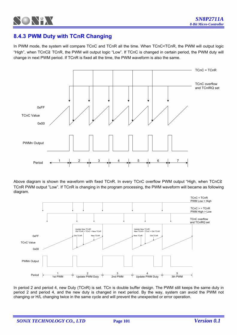
SN8P2711A 8-Bit Micro-Controller
SONiX TECHNOLOGY CO., LTD Page 101 Version 0.1
8.4.3 PWM Duty with TCnR Changing In PWM mode, the system will compare TCnC and TCnR all the time. When TCnC<TCnR, the PWM will output logic “High”, when TCnC≧ TCnR, the PWM will output logic “Low”. If TCnC is changed in certain period, the PWM duty will change in next PWM period. If TCnR is fixed all the time, the PWM waveform is also the same.
TCnC overflowand TCnIRQ set
TCnC = TCnR
0xFF
TCnC Value
0x00
PWMn Output
1 2 3 4 5 6 7Period
Above diagram is shown the waveform with fixed TCnR. In every TCnC overflow PWM output “High, when TCnC≧TCnR PWM output ”Low”. If TCnR is changing in the program processing, the PWM waveform will became as following diagram.
11st PWM
2Update PWM Duty
32nd PWM
4Update PWM Duty
0xFF
TCnC Value
0x00
PWMn Output
Period 53th PWM
TCnC overflowand TCnIRQ set
Old TCnR Old TCnRNew TCnR New TCnR
Update New TCnR!Old TCnR < TCnC < New TCnR
Update New TCnR!New TCnR < TCnC < Old TCnR
TCnC > = TCnRPWM High > Low
TCnC < TCnRPWM Low > High
In period 2 and period 4, new Duty (TCnR) is set. TCn is double buffer design. The PWM still keeps the same duty in period 2 and period 4, and the new duty is changed in next period. By the way, system can avoid the PWM not changing or H/L changing twice in the same cycle and will prevent the unexpected or error operation.
SN8P2711A 8-Bit Micro-Controller
SONiX TECHNOLOGY CO., LTD Page 102 Version 0.1
8.4.4 PWM PROGRAM EXAMPLE
Example: Setup PWM0 output from TC0 to PWM0OUT (P5.4). The external high-speed oscillator clock is 4MHz. Fcpu = Fosc/4. The duty of PWM is 30/256. The PWM frequency is about 1KHz. The PWM clock source is from external oscillator clock. TC0 rate is Fcpu/4. The TC0RATE2~TC0RATE1 = 110. TC0C = TC0R = 30.
MOV A,#01100000B B0MOV TC0M,A ; Set the TC0 rate to Fcpu/4 MOV A,#30 ; Set the PWM duty to 30/256 B0MOV TC0C,A B0MOV TC0R,A B0BCLR FTC0OUT ; Set duty range as 0/256~255/256. B0BCLR FALOAD0 B0BSET FPWM0OUT ; Enable PWM0 output to P5.4 and disable P5.4 I/O function B0BSET FTC0ENB ; Enable TC0 timer
Note: The TCnR is write-only register. Don’t process them using INCMS, DECMS instructions.
Example: Modify TC0R registers’ value. MOV A, #30H ; Input a number using B0MOV instruction. B0MOV TC0R, A INCMS BUF0 ; Get the new TC0R value from the BUF0 buffer defined by NOP ; programming. B0MOV A, BUF0 B0MOV TC0R, A
Note: The PWM can work with interrupt request.
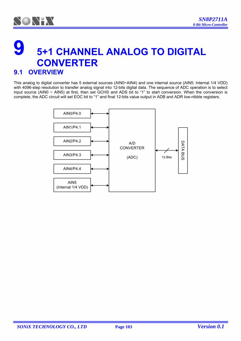
SN8P2711A 8-Bit Micro-Controller
SONiX TECHNOLOGY CO., LTD Page 103 Version 0.1
999 5+1 CHANNEL ANALOG TO DIGITAL CONVERTER
9.1 OVERVIEW This analog to digital converter has 5 external sources (AIN0~AIN4) and one internal source (AIN5: Internal 1/4 VDD) with 4096-step resolution to transfer analog signal into 12-bits digital data. The sequence of ADC operation is to select input source (AIN0 ~ AIN5) at first, then set GCHS and ADS bit to “1” to start conversion. When the conversion is complete, the ADC circuit will set EOC bit to “1” and final 12-bits value output in ADB and ADR low-nibble registers.
AIN0/P4.0
AIN1/P4.1
AIN2/P4.2
AIN3/P4.3
AIN4/P4.4
AIN5(Internal 1/4 VDD)
A/DCONVERTER
(ADC)
DATA B
US12-Bits
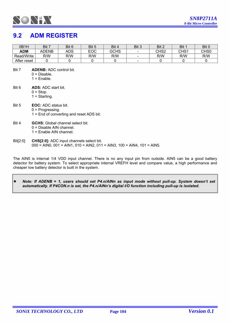
SN8P2711A 8-Bit Micro-Controller
SONiX TECHNOLOGY CO., LTD Page 104 Version 0.1
9.2 ADM REGISTER
0B1H Bit 7 Bit 6 Bit 5 Bit 4 Bit 3 Bit 2 Bit 1 Bit 0 ADM ADENB ADS EOC GCHS - CHS2 CHS1 CHS0
Read/Write R/W R/W R/W R/W - R/W R/W R/W After reset 0 0 0 0 - 0 0 0
Bit 7 ADENB: ADC control bit.
0 = Disable. 1 = Enable.
Bit 6 ADS: ADC start bit.
0 = Stop. 1 = Starting.
Bit 5 EOC: ADC status bit.
0 = Progressing. 1 = End of converting and reset ADS bit.
Bit 4 GCHS: Global channel select bit. 0 = Disable AIN channel. 1 = Enable AIN channel. Bit[2:0] CHS[2:0]: ADC input channels select bit. 000 = AIN0, 001 = AIN1, 010 = AIN2, 011 = AIN3, 100 = AIN4, 101 = AIN5. The AIN5 is internal 1/4 VDD input channel. There is no any input pin from outside. AIN5 can be a good battery detector for battery system. To select appropriate internal VREFH level and compare value, a high performance and cheaper low battery detector is built in the system.
Note: If ADENB = 1, users should set P4.n/AINn as input mode without pull-up. System doesn’t set automatically. If P4CON.n is set, the P4.n/AINn’s digital I/O function including pull-up is isolated.
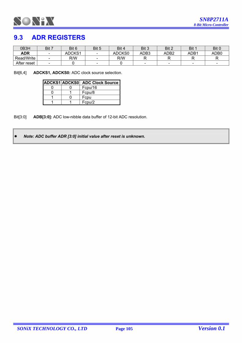
SN8P2711A 8-Bit Micro-Controller
SONiX TECHNOLOGY CO., LTD Page 105 Version 0.1
9.3 ADR REGISTERS
0B3H Bit 7 Bit 6 Bit 5 Bit 4 Bit 3 Bit 2 Bit 1 Bit 0 ADR - ADCKS1 - ADCKS0 ADB3 ADB2 ADB1 ADB0
Read/Write - R/W - R/W R R R R After reset - 0 - 0 - - - -
Bit[6,4] ADCKS1, ADCKS0: ADC clock source selection.
ADCKS1 ADCKS0 ADC Clock Source 0 0 Fcpu/16 0 1 Fcpu/8 1 0 Fcpu 1 1 Fcpu/2
Bit[3:0] ADB[3:0]: ADC low-nibble data buffer of 12-bit ADC resolution.
Note: ADC buffer ADR [3:0] initial value after reset is unknown.
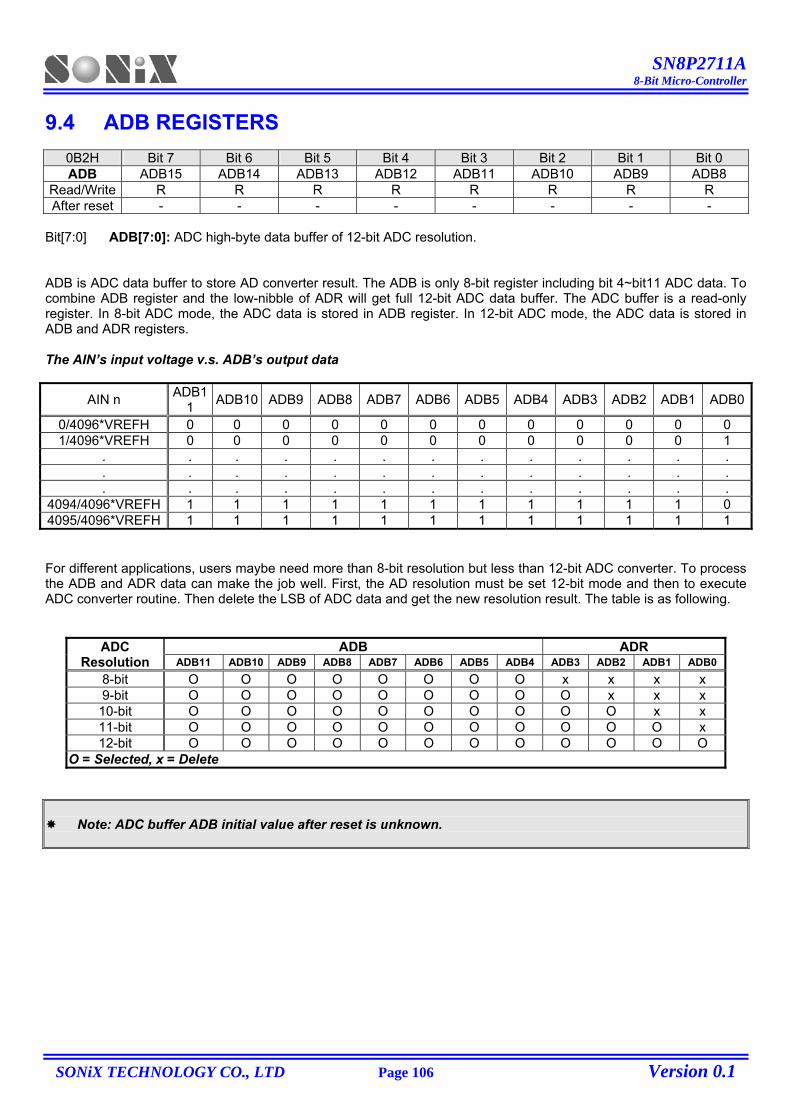
SN8P2711A 8-Bit Micro-Controller
SONiX TECHNOLOGY CO., LTD Page 106 Version 0.1
9.4 ADB REGISTERS
0B2H Bit 7 Bit 6 Bit 5 Bit 4 Bit 3 Bit 2 Bit 1 Bit 0 ADB ADB15 ADB14 ADB13 ADB12 ADB11 ADB10 ADB9 ADB8
Read/Write R R R R R R R R After reset - - - - - - - -
Bit[7:0] ADB[7:0]: ADC high-byte data buffer of 12-bit ADC resolution. ADB is ADC data buffer to store AD converter result. The ADB is only 8-bit register including bit 4~bit11 ADC data. To combine ADB register and the low-nibble of ADR will get full 12-bit ADC data buffer. The ADC buffer is a read-only register. In 8-bit ADC mode, the ADC data is stored in ADB register. In 12-bit ADC mode, the ADC data is stored in ADB and ADR registers. The AIN’s input voltage v.s. ADB’s output data
AIN n ADB11 ADB10 ADB9 ADB8 ADB7 ADB6 ADB5 ADB4 ADB3 ADB2 ADB1 ADB0
0/4096*VREFH 0 0 0 0 0 0 0 0 0 0 0 0 1/4096*VREFH 0 0 0 0 0 0 0 0 0 0 0 1
. . . . . . . . . . . . .
. . . . . . . . . . . . .
. . . . . . . . . . . . . 4094/4096*VREFH 1 1 1 1 1 1 1 1 1 1 1 0 4095/4096*VREFH 1 1 1 1 1 1 1 1 1 1 1 1 For different applications, users maybe need more than 8-bit resolution but less than 12-bit ADC converter. To process the ADB and ADR data can make the job well. First, the AD resolution must be set 12-bit mode and then to execute ADC converter routine. Then delete the LSB of ADC data and get the new resolution result. The table is as following.
ADB ADR ADC Resolution ADB11 ADB10 ADB9 ADB8 ADB7 ADB6 ADB5 ADB4 ADB3 ADB2 ADB1 ADB0
8-bit O O O O O O O O x x x x 9-bit O O O O O O O O O x x x 10-bit O O O O O O O O O O x x 11-bit O O O O O O O O O O O x 12-bit O O O O O O O O O O O O
O = Selected, x = Delete
Note: ADC buffer ADB initial value after reset is unknown.
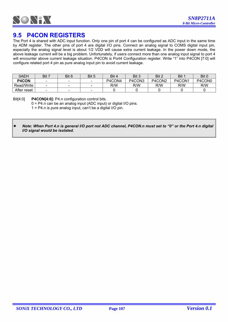
SN8P2711A 8-Bit Micro-Controller
SONiX TECHNOLOGY CO., LTD Page 107 Version 0.1
9.5 P4CON REGISTERS The Port 4 is shared with ADC input function. Only one pin of port 4 can be configured as ADC input in the same time by ADM register. The other pins of port 4 are digital I/O pins. Connect an analog signal to COMS digital input pin, especially the analog signal level is about 1/2 VDD will cause extra current leakage. In the power down mode, the above leakage current will be a big problem. Unfortunately, if users connect more than one analog input signal to port 4 will encounter above current leakage situation. P4CON is Port4 Configuration register. Write “1” into P4CON [7:0] will configure related port 4 pin as pure analog input pin to avoid current leakage.
0AEH Bit 7 Bit 6 Bit 5 Bit 4 Bit 3 Bit 2 Bit 1 Bit 0 P4CON - - - P4CON4 P4CON3 P4CON2 P4CON1 P4CON0
Read/Write - - - R/W R/W R/W R/W R/W After reset - - - 0 0 0 0 0
Bit[4:0] P4CON[4:0]: P4.n configuration control bits. 0 = P4.n can be an analog input (ADC input) or digital I/O pins. 1 = P4.n is pure analog input, can’t be a digital I/O pin.
Note: When Port 4.n is general I/O port not ADC channel, P4CON.n must set to “0” or the Port 4.n digital I/O signal would be isolated.
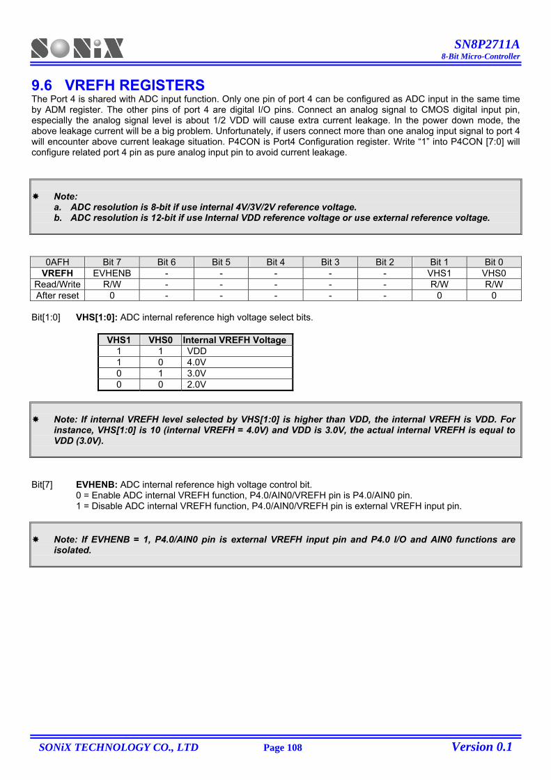
SN8P2711A 8-Bit Micro-Controller
SONiX TECHNOLOGY CO., LTD Page 108 Version 0.1
9.6 VREFH REGISTERS The Port 4 is shared with ADC input function. Only one pin of port 4 can be configured as ADC input in the same time by ADM register. The other pins of port 4 are digital I/O pins. Connect an analog signal to CMOS digital input pin, especially the analog signal level is about 1/2 VDD will cause extra current leakage. In the power down mode, the above leakage current will be a big problem. Unfortunately, if users connect more than one analog input signal to port 4 will encounter above current leakage situation. P4CON is Port4 Configuration register. Write “1” into P4CON [7:0] will configure related port 4 pin as pure analog input pin to avoid current leakage.
Note: a. ADC resolution is 8-bit if use internal 4V/3V/2V reference voltage. b. ADC resolution is 12-bit if use Internal VDD reference voltage or use external reference voltage.
0AFH Bit 7 Bit 6 Bit 5 Bit 4 Bit 3 Bit 2 Bit 1 Bit 0 VREFH EVHENB - - - - - VHS1 VHS0
Read/Write R/W - - - - - R/W R/W After reset 0 - - - - - 0 0
Bit[1:0] VHS[1:0]: ADC internal reference high voltage select bits.
VHS1 VHS0 Internal VREFH Voltage1 1 VDD 1 0 4.0V 0 1 3.0V 0 0 2.0V
Note: If internal VREFH level selected by VHS[1:0] is higher than VDD, the internal VREFH is VDD. For instance, VHS[1:0] is 10 (internal VREFH = 4.0V) and VDD is 3.0V, the actual internal VREFH is equal to VDD (3.0V).
Bit[7] EVHENB: ADC internal reference high voltage control bit.
0 = Enable ADC internal VREFH function, P4.0/AIN0/VREFH pin is P4.0/AIN0 pin. 1 = Disable ADC internal VREFH function, P4.0/AIN0/VREFH pin is external VREFH input pin.
Note: If EVHENB = 1, P4.0/AIN0 pin is external VREFH input pin and P4.0 I/O and AIN0 functions are isolated.
SN8P2711A 8-Bit Micro-Controller
SONiX TECHNOLOGY CO., LTD Page 109 Version 0.1
9.7 ADC CONVERTING TIME
12-bit ADC conversion time = 1/(ADC clock /4)*16 sec
High Clock (Fosc) = 4MHz
Fcpu ADCKS1 ADCKS0 ADC Clock ADC Converting Time 0 0 Fcpu/16 1/( ( 4MHz / 1 ) / 16 /4 ) x16= 256 us0 1 Fcpu/8 1/( ( 4MHz / 1 ) / 8 /4 ) x16= 128 us1 0 Fcpu 1/( ( 4MHz / 1 ) / 1 /4 ) x16= 16 us
Fosc/ 1
1 1 Fcpu/2 1/( ( 4MHz / 1 ) / 2 /4 ) x16= 32 us0 0 Fcpu/16 1/( ( 4MHz / 2 ) / 16 /4 ) x16= 512 us0 1 Fcpu/8 1/( ( 4MHz / 2 ) / 8 /4 ) x16= 256 us1 0 Fcpu 1/( ( 4MHz / 2 ) / 1 /4 ) x16= 32 us
Fosc/ 2
1 1 Fcpu/2 1/( ( 4MHz / 2 ) / 2 /4 ) x16= 64 us0 0 Fcpu/16 1/( ( 4MHz / 4 ) / 16 /4 ) x16= 1024 us0 1 Fcpu/8 1/( ( 4MHz / 4 ) / 8 /4 ) x16= 512 us1 0 Fcpu 1/( ( 4MHz / 4 ) / 1 /4 ) x16= 64 us
Fosc/ 4
1 1 Fcpu/2 1/( ( 4MHz / 4 ) / 2 /4 ) x16= 128 us0 0 Fcpu/16 1/( ( 4MHz / 8 ) / 16 /4 ) x16= 2048 us0 1 Fcpu/8 1/( ( 4MHz / 8 ) / 8 /4 ) x16= 1024 us1 0 Fcpu 1/( ( 4MHz / 8 ) / 1 /4 ) x16= 128 us
Fosc/ 8
1 1 Fcpu/2 1/( ( 4MHz / 8 ) / 2 /4 ) x16= 256 us0 0 Fcpu/16 1/( ( 4MHz / 16 ) / 16 /4 ) x16= 4096 us0 1 Fcpu/8 1/( ( 4MHz / 16 ) / 8 /4 ) x16= 2048 us1 0 Fcpu 1/( ( 4MHz / 16 ) / 1 /4 ) x16= 256 us
Fosc/ 16
1 1 Fcpu/2 1/( ( 4MHz / 16 ) / 2 /4 ) x16= 512 us
SN8P2711A 8-Bit Micro-Controller
SONiX TECHNOLOGY CO., LTD Page 110 Version 0.1
9.8 ADC ROUTINE EXAMPLE
Example : To set AIN0 for ADC input and executing 12-bit ADC. VREFH is internal 3.0V. ADC clock source is Fcpu.
; Enable ADC function and delay 100us for conversion. ADC0: B0BSET FADENB ; Enable ADC circuit CALL Delay100uS ; Delay 100uS to wait ADC circuit ready for conversion. ; Set Port 4 I/O mode. MOV A, #0FEH B0MOV P4UR, A ; Disable P4.0 pull-up resistor. B0BCLR FP40M ; Set P4.0 as input pin. ; or MOV A, #01H B0MOV P4CON, A ; Set P4.0 as pure analog input. ; Set VREFH is internal 3.0V. MOV A, #01H B0MOV VREFH, A ; Set internal 3.0V VREFH. ; Set ADC clock source = Fcpu. MOV A, #40H B0MOV ADR, A ; To set ADC clock = Fcpu. ; Enable AIN0 (P4.0). MOV A, #90H B0MOV ADM, A ; To enable ADC and set AIN0 input ; Start AD conversion. B0BSET FADS ; To start conversion WADC0: B0BTS1 FEOC ; To skip, if end of converting =1 JMP WADC0 ; else, jump to WADC0 B0MOV A, ADB ; To get AIN0 input data bit11 ~ bit4 B0MOV Adc_Buf_Hi, A B0MOV A, ADR ; To get AIN0 input data bit3 ~ bit0 AND A, 0FH B0MOV Adc_Buf_Low, A End_ADC: . B0BCLR FADENB ; Disable ADC circuit
SN8P2711A 8-Bit Micro-Controller
SONiX TECHNOLOGY CO., LTD Page 111 Version 0.1
Example : To set AIN1 for ADC input and executing 12-bit ADC. VREFH is external input voltage from
VREFH pin (P4.0/AIN0). ADC clock source is Fcpu. Using ADC interrupt. ; Enable ADC function and delay 100us for conversion. ADC0: B0BSET FADENB ; Enable ADC circuit CALL Delay100uS ; Delay 100uS to wait ADC circuit ready for conversion. ; Set Port 4 I/O mode. MOV A, #0FDH B0MOV P4UR, A ; Disable P4.1 pull-up resistor. B0BCLR FP41M ; Set P4.1 as input pin. ; or MOV A, #02H B0MOV P4CON, A ; Set P4.1 as pure analog input. ; Set VREFH is external input voltage. B0BSET EVHENB ; Enable external VREFH input. ; Set ADC clock source = Fcpu. MOV A, #40H B0MOV ADR, A ; To set ADC clock = Fcpu. ; Enable AIN0 (P4.1). MOV A, #91H B0MOV ADM,A ; To enable ADC and set AIN1 input ; Set ADC interrupt. B0BCLR FADCIRQ ; Clear ADC interrupt request flag. B0BSET FADCIEN ; Enable ADC interrupt function. B0BSET FGIE ; Enable Global interrupt function. ; Start AD conversion. B0BSET FADS ; To start conversion … … … ADC_INT_SR: PUSH B0BTS1 FADCIRQ ; Check ADC interrupt flag. JMP ADC_INT_EXIT B0BCLR FADCIRQ ; Clear ADC interrupt request flag. B0MOV A, ADB ; To get AIN0 input data bit11 ~ bit4 B0MOV Adc_Buf_Hi, A B0MOV A, ADR ; To get AIN0 input data bit3 ~ bit0 AND A, 0FH B0MOV Adc_Buf_Low, A B0BCLR FADENB ; Disable ADC circuit ADC_INT_EXIT: . POP RETI
SN8P2711A 8-Bit Micro-Controller
SONiX TECHNOLOGY CO., LTD Page 112 Version 0.1
9.9 ADC CIRCUIT
MCU
VCC
GND
AINn/P4.n
VDD
VSS
0.1uF
Analog Signal Input
47uF
0.1uF
ADC reference high voltage is internal reference voltage and VREFH pin is AIN0/P4.0. The capacitor (0.1uF) between AINn/P4.n and VSS is necessary to stable analog signal.
MCU
VCC
GND
VREFH
AINn/P4.n
VDD
VSS
0.1uF
Analog Signal Input
47uF
0.1uF
ADC reference high voltage is from VDD pin and AIN0/P4.0 is VERFH input. The VERFH should be from MCU’s VDD pin. Don’t connect from main power.
MCU
VCC
GND
VREFH
AINn/P4.n
VDD
VSS
0.1uF
Analog Signal Input
0.1uF
47uF
Reference High Voltage Input
ADC reference high voltage is from external voltage and AIN0/P4.0 is VERFH input. The capacitor (47uF) between VREFH and VSS is necessary to stable VERFH voltage.
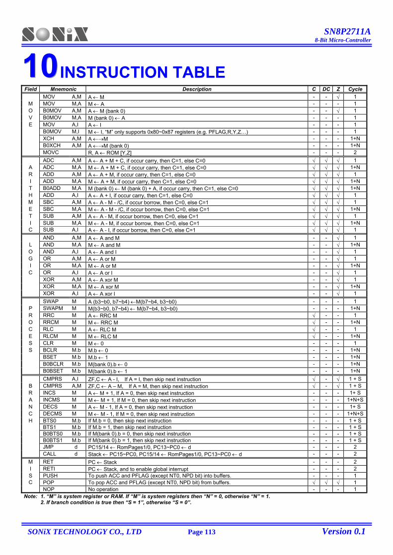
SN8P2711A 8-Bit Micro-Controller
SONiX TECHNOLOGY CO., LTD Page 113 Version 0.1
111000 INSTRUCTION TABLE Field Mnemonic Description C DC Z Cycle
MOV A,M A ← M - - √ 1 M MOV M,A M ← A - - - 1 O B0MOV A,M A ← M (bank 0) - - √ 1 V B0MOV M,A M (bank 0) ← A - - - 1 E MOV A,I A ← I - - - 1 B0MOV M,I M ← I, “M” only supports 0x80~0x87 registers (e.g. PFLAG,R,Y,Z…) - - - 1 XCH A,M A ←→M - - - 1+N B0XCH A,M A ←→M (bank 0) - - - 1+N MOVC R, A ← ROM [Y,Z] - - - 2 ADC A,M A ← A + M + C, if occur carry, then C=1, else C=0 √ √ √ 1
A ADC M,A M ← A + M + C, if occur carry, then C=1, else C=0 √ √ √ 1+N R ADD A,M A ← A + M, if occur carry, then C=1, else C=0 √ √ √ 1 I ADD M,A M ← A + M, if occur carry, then C=1, else C=0 √ √ √ 1+N T B0ADD M,A M (bank 0) ← M (bank 0) + A, if occur carry, then C=1, else C=0 √ √ √ 1+N H ADD A,I A ← A + I, if occur carry, then C=1, else C=0 √ √ √ 1 M SBC A,M A ← A - M - /C, if occur borrow, then C=0, else C=1 √ √ √ 1 E SBC M,A M ← A - M - /C, if occur borrow, then C=0, else C=1 √ √ √ 1+N T SUB A,M A ← A - M, if occur borrow, then C=0, else C=1 √ √ √ 1 I SUB M,A M ← A - M, if occur borrow, then C=0, else C=1 √ √ √ 1+N C SUB A,I A ← A - I, if occur borrow, then C=0, else C=1 √ √ √ 1 AND A,M A ← A and M - - √ 1 L AND M,A M ← A and M - - √ 1+N O AND A,I A ← A and I - - √ 1 G OR A,M A ← A or M - - √ 1 I OR M,A M ← A or M - - √ 1+N C OR A,I A ← A or I - - √ 1 XOR A,M A ← A xor M - - √ 1 XOR M,A M ← A xor M - - √ 1+N XOR A,I A ← A xor I - - √ 1 SWAP M A (b3~b0, b7~b4) ←M(b7~b4, b3~b0) - - - 1
P SWAPM M M(b3~b0, b7~b4) ← M(b7~b4, b3~b0) - - - 1+N R RRC M A ← RRC M √ - - 1 O RRCM M M ← RRC M √ - - 1+N C RLC M A ← RLC M √ - - 1 E RLCM M M ← RLC M √ - - 1+N S CLR M M ← 0 - - - 1 S BCLR M.b M.b ← 0 - - - 1+N BSET M.b M.b ← 1 - - - 1+N B0BCLR M.b M(bank 0).b ← 0 - - - 1+N B0BSET M.b M(bank 0).b ← 1 - - - 1+N CMPRS A,I ZF,C ← A - I, If A = I, then skip next instruction √ - √ 1 + S
B CMPRS A,M ZF,C ← A – M, If A = M, then skip next instruction √ - √ 1 + SR INCS M A ← M + 1, If A = 0, then skip next instruction - - - 1+ SA INCMS M M ← M + 1, If M = 0, then skip next instruction - - - 1+N+SN DECS M A ← M - 1, If A = 0, then skip next instruction - - - 1+ SC DECMS M M ← M - 1, If M = 0, then skip next instruction - - - 1+N+SH BTS0 M.b If M.b = 0, then skip next instruction - - - 1 + S BTS1 M.b If M.b = 1, then skip next instruction - - - 1 + S B0BTS0 M.b If M(bank 0).b = 0, then skip next instruction - - - 1 + S B0BTS1 M.b If M(bank 0).b = 1, then skip next instruction - - - 1 + S JMP d PC15/14 ← RomPages1/0, PC13~PC0 ← d - - - 2 CALL d Stack ← PC15~PC0, PC15/14 ← RomPages1/0, PC13~PC0 ← d - - - 2
M RET PC ← Stack - - - 2 I RETI PC ← Stack, and to enable global interrupt - - - 2 S PUSH To push ACC and PFLAG (except NT0, NPD bit) into buffers. - - - 1 C POP To pop ACC and PFLAG (except NT0, NPD bit) from buffers. √ √ √ 1 NOP No operation - - - 1
Note: 1. “M” is system register or RAM. If “M” is system registers then “N” = 0, otherwise “N” = 1. 2. If branch condition is true then “S = 1”, otherwise “S = 0”.
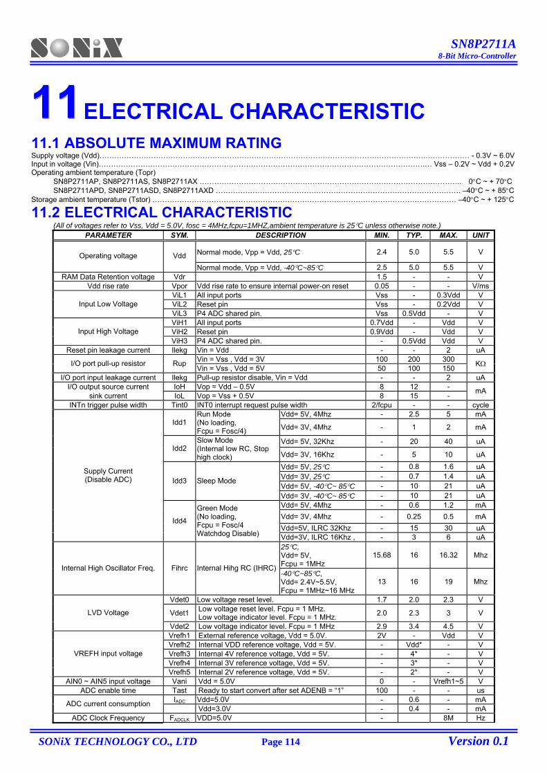
SN8P2711A 8-Bit Micro-Controller
SONiX TECHNOLOGY CO., LTD Page 114 Version 0.1
111111 ELECTRICAL CHARACTERISTIC
11.1 ABSOLUTE MAXIMUM RATING Supply voltage (Vdd)…………………………………………………………………………………………………………………….……………… - 0.3V ~ 6.0VInput in voltage (Vin)…………………………………………………………………………………………………………………….… Vss – 0.2V ~ Vdd + 0.2VOperating ambient temperature (Topr) SN8P2711AP, SN8P2711AS, SN8P2711AX …………………………………………………………………………………………….. 0°C ~ + 70°C SN8P2711APD, SN8P2711ASD, SN8P2711AXD ………………………………………………………………………………………. –40°C ~ + 85°CStorage ambient temperature (Tstor) ………………………………………………………………….………………………………………… –40°C ~ + 125°C
11.2 ELECTRICAL CHARACTERISTIC (All of voltages refer to Vss, Vdd = 5.0V, fosc = 4MHz,fcpu=1MHZ,ambient temperature is 25°C unless otherwise note.)
PARAMETER SYM. DESCRIPTION MIN. TYP. MAX. UNIT
Normal mode, Vpp = Vdd, 25°C 2.4 5.0 5.5 V Operating voltage Vdd Normal mode, Vpp = Vdd, -40°C~85°C 2.5 5.0 5.5 V
RAM Data Retention voltage Vdr 1.5 - - V Vdd rise rate Vpor Vdd rise rate to ensure internal power-on reset 0.05 - - V/ms
ViL1 All input ports Vss - 0.3Vdd V ViL2 Reset pin Vss - 0.2Vdd V Input Low Voltage ViL3 P4 ADC shared pin. Vss 0.5Vdd - V ViH1 All input ports 0.7Vdd - Vdd V ViH2 Reset pin 0.9Vdd - Vdd V Input High Voltage ViH3 P4 ADC shared pin. - 0.5Vdd Vdd V
Reset pin leakage current Ilekg Vin = Vdd - - 2 uA Vin = Vss , Vdd = 3V 100 200 300 I/O port pull-up resistor Rup Vin = Vss , Vdd = 5V 50 100 150 KΩ
I/O port input leakage current Ilekg Pull-up resistor disable, Vin = Vdd - - 2 uA I/O output source current IoH Vop = Vdd – 0.5V 8 12 -
sink current IoL Vop = Vss + 0.5V 8 15 - mA
INTn trigger pulse width Tint0 INT0 interrupt request pulse width 2/fcpu - - cycleVdd= 5V, 4Mhz - 2.5 5 mA
Idd1 Run Mode (No loading, Fcpu = Fosc/4) Vdd= 3V, 4Mhz - 1 2 mA
Vdd= 5V, 32Khz - 20 40 uA Idd2
Slow Mode (Internal low RC, Stop high clock) Vdd= 3V, 16Khz - 5 10 uA
Vdd= 5V, 25°C - 0.8 1.6 uA Vdd= 3V, 25°C - 0.7 1.4 uA Vdd= 5V, -40°C~ 85°C - 10 21 uA
Idd3 Sleep Mode
Vdd= 3V, -40°C~ 85°C - 10 21 uA Vdd= 5V, 4Mhz - 0.6 1.2 mAVdd= 3V, 4Mhz - 0.25 0.5 mAVdd=5V, ILRC 32Khz - 15 30 uA
Supply Current (Disable ADC)
Idd4
Green Mode (No loading, Fcpu = Fosc/4 Watchdog Disable) Vdd=3V, ILRC 16Khz , - 3 6 uA
25°C, Vdd= 5V, Fcpu = 1MHz
15.68 16 16.32 Mhz
Internal High Oscillator Freq. Fihrc Internal Hihg RC (IHRC)-40°C~85°C, Vdd= 2.4V~5.5V, Fcpu = 1MHz~16 MHz
13 16 19 Mhz
Vdet0 Low voltage reset level. 1.7 2.0 2.3 V
Vdet1 Low voltage reset level. Fcpu = 1 MHz. Low voltage indicator level. Fcpu = 1 MHz. 2.0 2.3 3 V LVD Voltage
Vdet2 Low voltage indicator level. Fcpu = 1 MHz 2.9 3.4 4.5 V Vrefh1 External reference voltage, Vdd = 5.0V. 2V - Vdd V Vrefh2 Internal VDD reference voltage, Vdd = 5V. - Vdd* - V Vrefh3 Internal 4V reference voltage, Vdd = 5V. - 4* - V Vrefh4 Internal 3V reference voltage, Vdd = 5V. - 3* - V
VREFH input voltage
Vrefh5 Internal 2V reference voltage, Vdd = 5V. - 2* - V AIN0 ~ AIN5 input voltage Vani Vdd = 5.0V 0 - Vrefh1~5 V
ADC enable time Tast Ready to start convert after set ADENB = “1” 100 - - us IADC Vdd=5.0V - 0.6 - mAADC current consumption
Vdd=3.0V - 0.4 - mAADC Clock Frequency FADCLK VDD=5.0V - 8M Hz
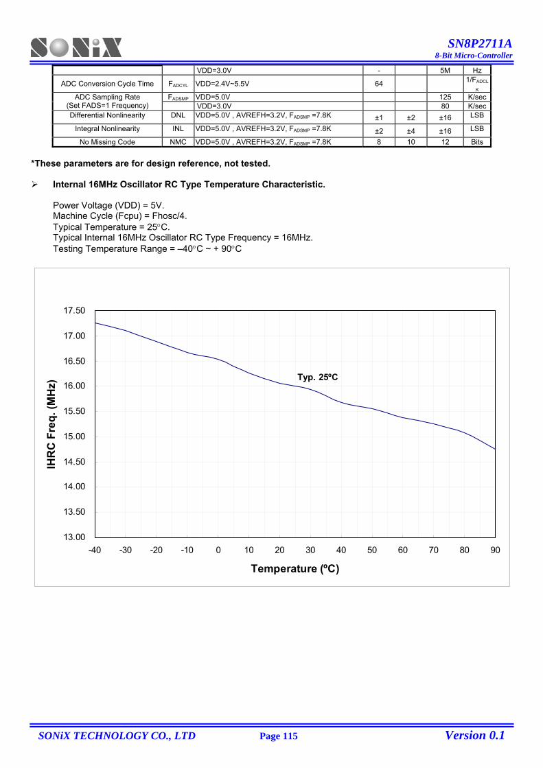
SN8P2711A 8-Bit Micro-Controller
SONiX TECHNOLOGY CO., LTD Page 115 Version 0.1
VDD=3.0V - 5M Hz
ADC Conversion Cycle Time FADCYL VDD=2.4V~5.5V 64 1/FADCL
K FADSMP VDD=5.0V 125 K/secADC Sampling Rate
(Set FADS=1 Frequency) VDD=3.0V 80 K/secDifferential Nonlinearity DNL VDD=5.0V , AVREFH=3.2V, FADSMP =7.8K ±1 ±2 ±16 LSB
Integral Nonlinearity INL VDD=5.0V , AVREFH=3.2V, FADSMP =7.8K ±2 ±4 ±16 LSB
No Missing Code NMC VDD=5.0V , AVREFH=3.2V, FADSMP =7.8K 8 10 12 Bits *These parameters are for design reference, not tested.
Internal 16MHz Oscillator RC Type Temperature Characteristic. Power Voltage (VDD) = 5V. Machine Cycle (Fcpu) = Fhosc/4. Typical Temperature = 25°C. Typical Internal 16MHz Oscillator RC Type Frequency = 16MHz. Testing Temperature Range = –40°C ~ + 90°C
Typ. 25ºC
13.00
13.50
14.00
14.50
15.00
15.50
16.00
16.50
17.00
17.50
-40 -30 -20 -10 0 10 20 30 40 50 60 70 80 90
Temperature (ºC)
IHR
C F
req.
(MH
z)
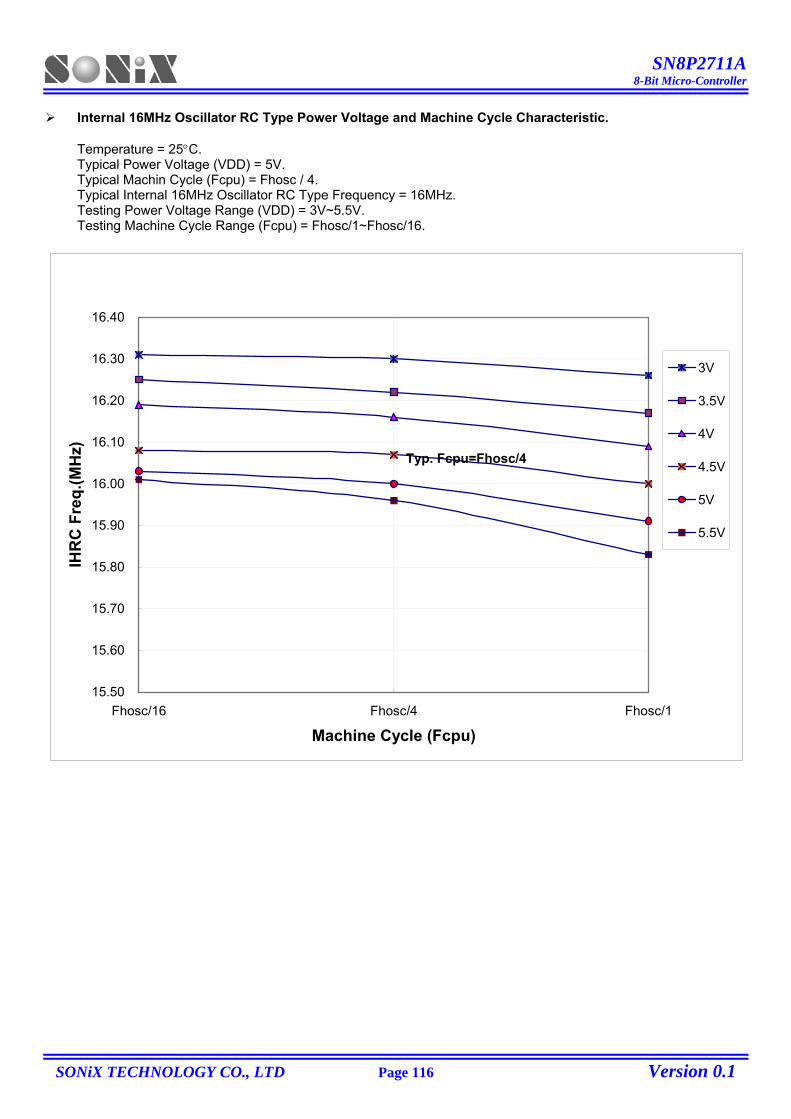
SN8P2711A 8-Bit Micro-Controller
SONiX TECHNOLOGY CO., LTD Page 116 Version 0.1
Internal 16MHz Oscillator RC Type Power Voltage and Machine Cycle Characteristic.
Temperature = 25°C. Typical Power Voltage (VDD) = 5V. Typical Machin Cycle (Fcpu) = Fhosc / 4. Typical Internal 16MHz Oscillator RC Type Frequency = 16MHz. Testing Power Voltage Range (VDD) = 3V~5.5V. Testing Machine Cycle Range (Fcpu) = Fhosc/1~Fhosc/16.
Typ. Fcpu=Fhosc/4
15.50
15.60
15.70
15.80
15.90
16.00
16.10
16.20
16.30
16.40
Fhosc/16 Fhosc/4 Fhosc/1
Machine Cycle (Fcpu)
IHR
C F
req.
(MH
z)
3V
3.5V
4V
4.5V
5V
5.5V
SN8P2711A 8-Bit Micro-Controller
SONiX TECHNOLOGY CO., LTD Page 117 Version 0.1
111222 DEVELOPMENT TOOL VERSION 12.1 ICE (In Circuit Emulation)
SN8ICE 2K ICE: Full function emulates SN8P2711A.
SN8ICE 2K ICE emulation notice: a. Operation voltage of ICE: 3.0V ~ 5.0V. b. Recommend maximum emulation speed at 5V: 8 MIPS (e.g. 16Mhz Crystal and Fcpu = Fhosc/2). c. Internal 16M RC precision is bad than real chip. d. Use SN8P2711 EV-KIT to emulate LVD and ADC reference voltage configuration.
Note: S8KD-2 ICE doesn’t support SN8P2711A emulation.
12.2 OTP WRITER Easy Writer V1.0:
OTP programming is controlled by ICE without firmware upgrade suffers. Please refer easy writer user manual for detailed information.
In SN8P2711A OTP programming by Easy Writer, the crystal of ICE must be 16MHz. Connect Easy Writer to ICE through a 60-pin cable which shipping with Easy Writer.
MP-Easy Writer V1.0: Stand-alone operation to support SN8P2711A mass production.
Note: Writer 3.0 doesn’t support SN8P2711A programming.
12.3 SN8IDE SONiX 8-bit MCU integrated development environment include Assembler, ICE debugger and OTP writer software.
For SN8ICE 2K: M2IDE_V113 or later. For Easy Writer and MP-Easy Writer: M2IDE_V107 or later
Note: SN8IDE (SN8IED_1.99R…) and SN8WTxxx don’t support SN8P2711A emulation.
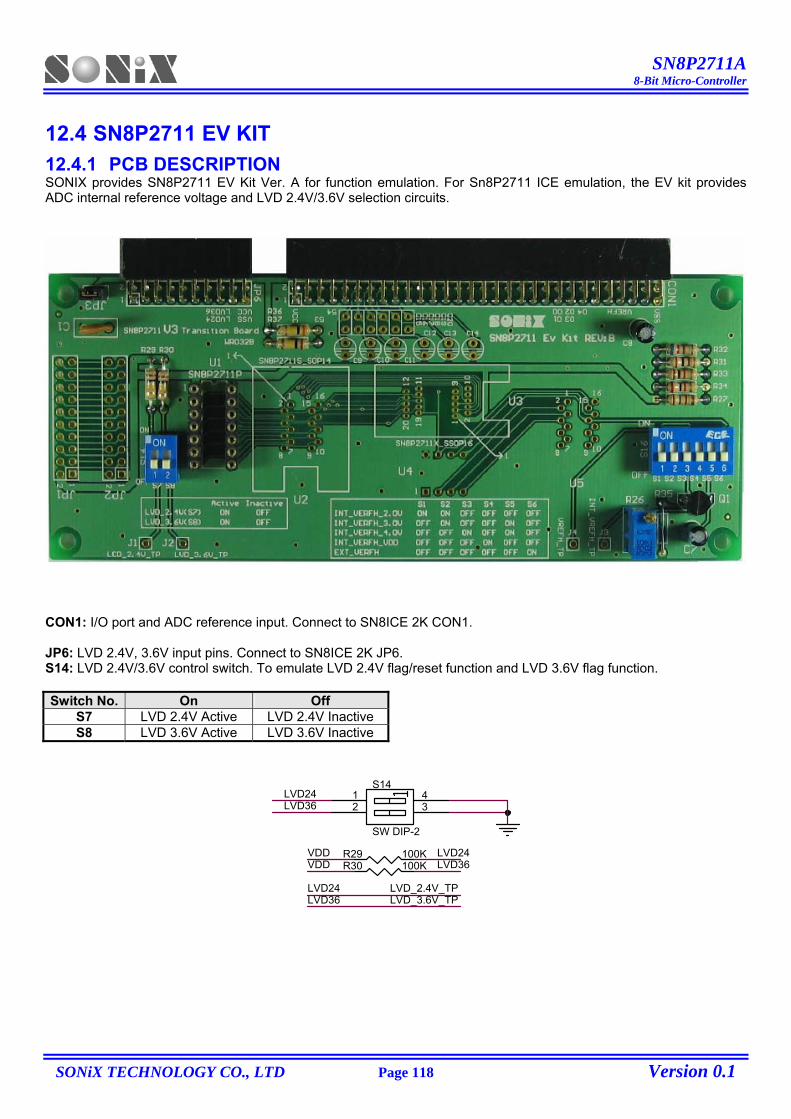
SN8P2711A 8-Bit Micro-Controller
SONiX TECHNOLOGY CO., LTD Page 118 Version 0.1
12.4 SN8P2711 EV KIT 12.4.1 PCB DESCRIPTION SONIX provides SN8P2711 EV Kit Ver. A for function emulation. For Sn8P2711 ICE emulation, the EV kit provides ADC internal reference voltage and LVD 2.4V/3.6V selection circuits.
CON1: I/O port and ADC reference input. Connect to SN8ICE 2K CON1. JP6: LVD 2.4V, 3.6V input pins. Connect to SN8ICE 2K JP6. S14: LVD 2.4V/3.6V control switch. To emulate LVD 2.4V flag/reset function and LVD 3.6V flag function. Switch No. On Off
S7 LVD 2.4V Active LVD 2.4V Inactive S8 LVD 3.6V Active LVD 3.6V Inactive
LVD36 LVD_3.6V_TP
LVD24
LVD24
LVD36
LVD36R29 100KR30 100K
VDD
LVD24 LVD_2.4V_TP
VDD
S14
SW DIP-2
12
43
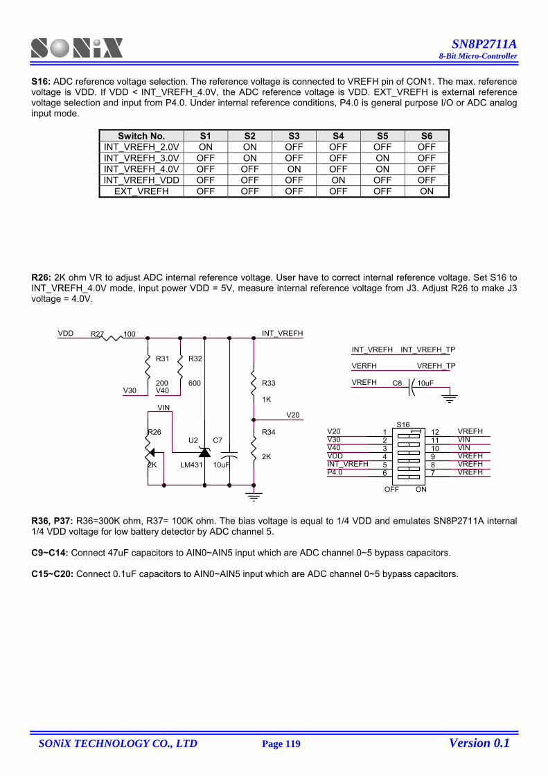
SN8P2711A 8-Bit Micro-Controller
SONiX TECHNOLOGY CO., LTD Page 119 Version 0.1
S16: ADC reference voltage selection. The reference voltage is connected to VREFH pin of CON1. The max. reference voltage is VDD. If VDD < INT_VREFH_4.0V, the ADC reference voltage is VDD. EXT_VREFH is external reference voltage selection and input from P4.0. Under internal reference conditions, P4.0 is general purpose I/O or ADC analog input mode.
R26: 2K ohm VR to adjust ADC internal reference voltage. User have to correct internal reference voltage. Set S16 to INT_VREFH_4.0V mode, input power VDD = 5V, measure internal reference voltage from J3. Adjust R26 to make J3 voltage = 4.0V.
VDD
R32
600
INT_VREFH
VIN
U2
LM431 VREFH
V40
V20
INT_VREFH_TP
C8 10uFR33
1K
VIN
INT_VREFH
INT_VREFH
R27 100
V20
VREFH
VERFH
VIN
R31
200
VREFH
V30
VREFH_TP
S16
OFF ON
123456
121110987
VDD
P4.0
C7
10uF
V40
VREFH
V30
R26
2K
VREFH
R34
2K
R36, P37: R36=300K ohm, R37= 100K ohm. The bias voltage is equal to 1/4 VDD and emulates SN8P2711A internal 1/4 VDD voltage for low battery detector by ADC channel 5. C9~C14: Connect 47uF capacitors to AIN0~AIN5 input which are ADC channel 0~5 bypass capacitors. C15~C20: Connect 0.1uF capacitors to AIN0~AIN5 input which are ADC channel 0~5 bypass capacitors.
Switch No. S1 S2 S3 S4 S5 S6 INT_VREFH_2.0V ON ON OFF OFF OFF OFF INT_VREFH_3.0V OFF ON OFF OFF ON OFF INT_VREFH_4.0V OFF OFF ON OFF ON OFF INT_VREFH_VDD OFF OFF OFF ON OFF OFF
EXT_VREFH OFF OFF OFF OFF OFF ON
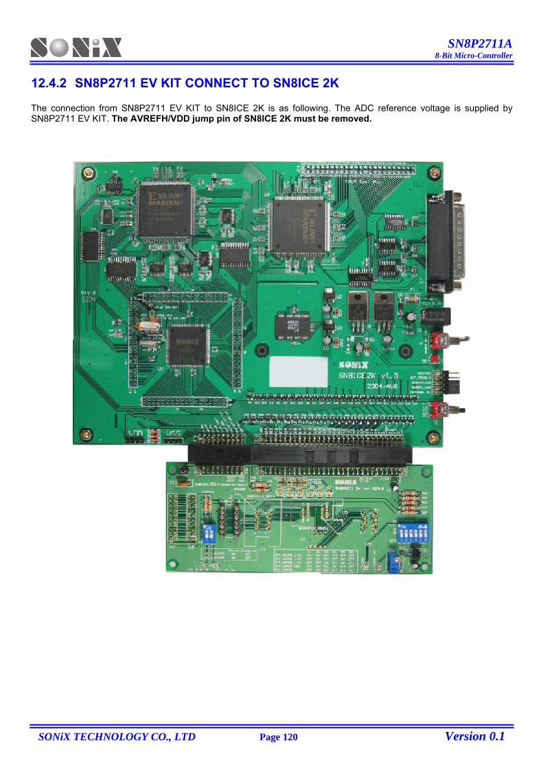
SN8P2711A 8-Bit Micro-Controller
SONiX TECHNOLOGY CO., LTD Page 120 Version 0.1
12.4.2 SN8P2711 EV KIT CONNECT TO SN8ICE 2K The connection from SN8P2711 EV KIT to SN8ICE 2K is as following. The ADC reference voltage is supplied by SN8P2711 EV KIT. The AVREFH/VDD jump pin of SN8ICE 2K must be removed.
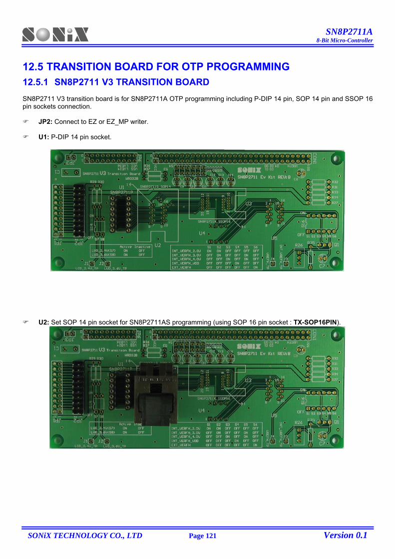
SN8P2711A 8-Bit Micro-Controller
SONiX TECHNOLOGY CO., LTD Page 121 Version 0.1
12.5 TRANSITION BOARD FOR OTP PROGRAMMING 12.5.1 SN8P2711 V3 TRANSITION BOARD SN8P2711 V3 transition board is for SN8P2711A OTP programming including P-DIP 14 pin, SOP 14 pin and SSOP 16 pin sockets connection.
JP2: Connect to EZ or EZ_MP writer.
U1: P-DIP 14 pin socket.
U2: Set SOP 14 pin socket for SN8P2711AS programming (using SOP 16 pin socket : TX-SOP16PIN).
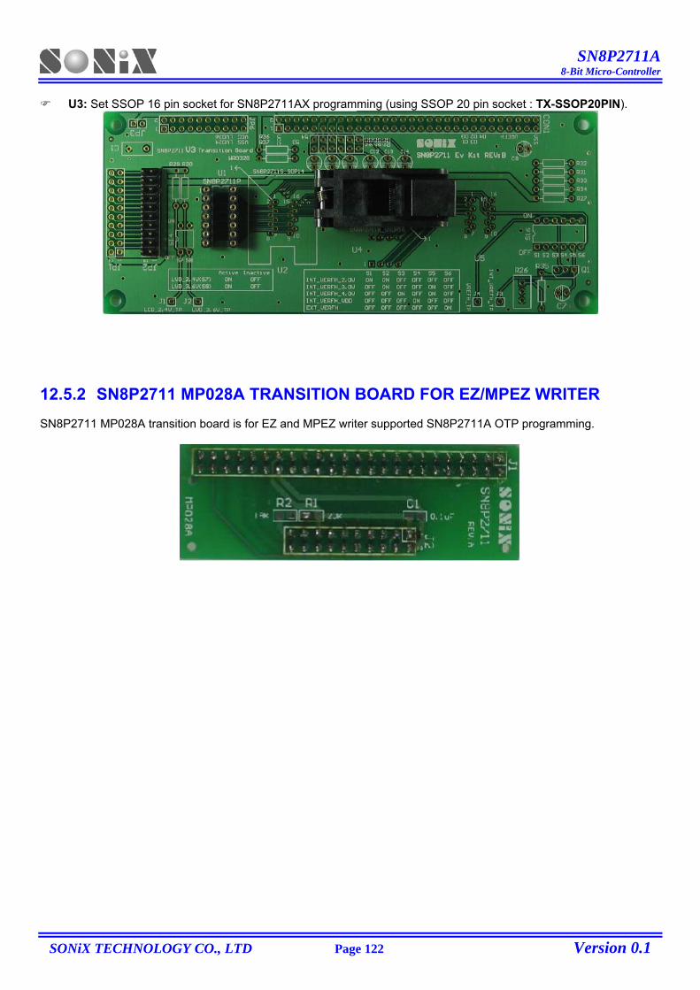
SN8P2711A 8-Bit Micro-Controller
SONiX TECHNOLOGY CO., LTD Page 122 Version 0.1
U3: Set SSOP 16 pin socket for SN8P2711AX programming (using SSOP 20 pin socket : TX-SSOP20PIN).
12.5.2 SN8P2711 MP028A TRANSITION BOARD FOR EZ/MPEZ WRITER SN8P2711 MP028A transition board is for EZ and MPEZ writer supported SN8P2711A OTP programming.
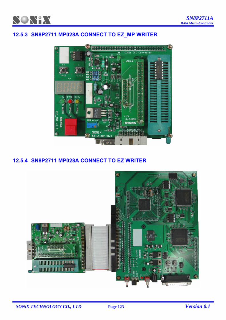
SN8P2711A 8-Bit Micro-Controller
SONiX TECHNOLOGY CO., LTD Page 123 Version 0.1
12.5.3 SN8P2711 MP028A CONNECT TO EZ_MP WRITER
12.5.4 SN8P2711 MP028A CONNECT TO EZ WRITER
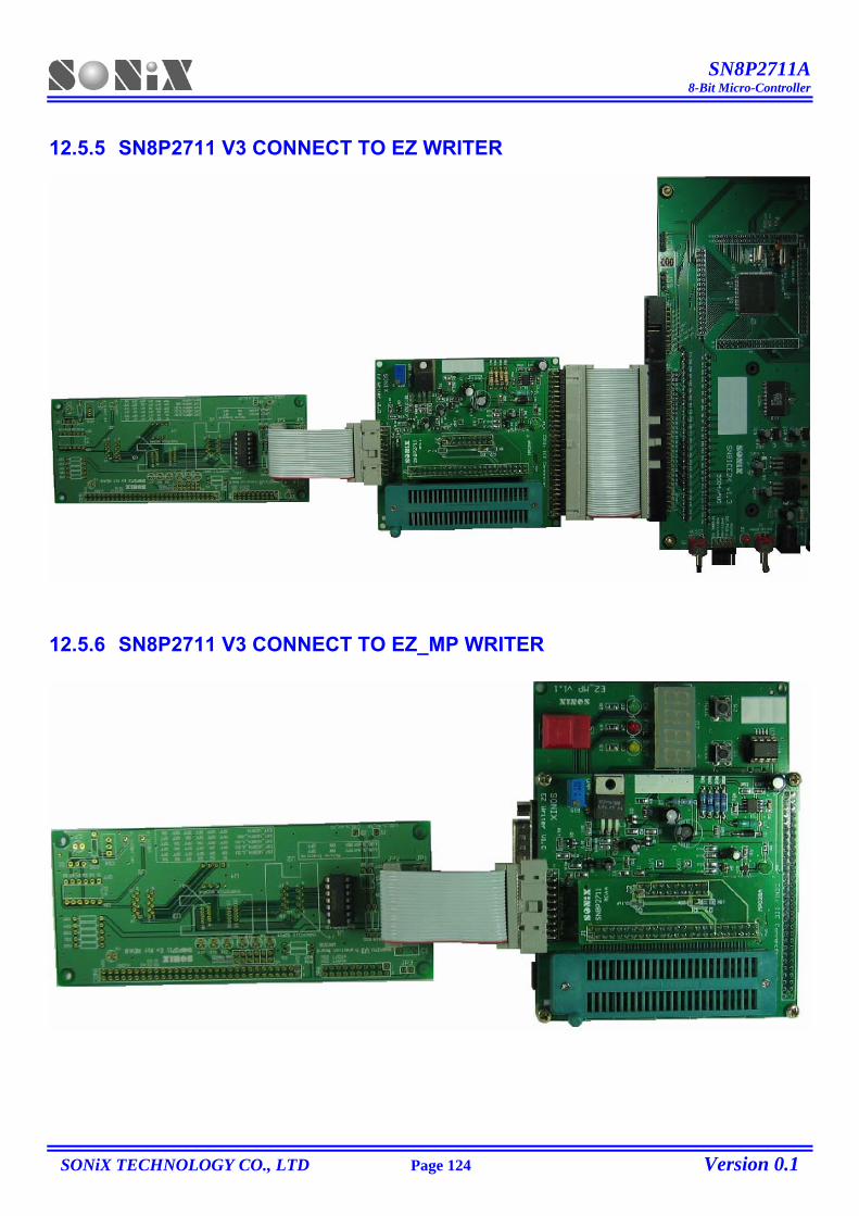
SN8P2711A 8-Bit Micro-Controller
SONiX TECHNOLOGY CO., LTD Page 124 Version 0.1
12.5.5 SN8P2711 V3 CONNECT TO EZ WRITER
12.5.6 SN8P2711 V3 CONNECT TO EZ_MP WRITER
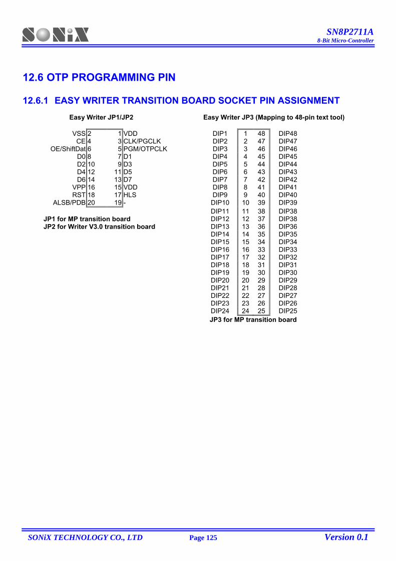
SN8P2711A 8-Bit Micro-Controller
SONiX TECHNOLOGY CO., LTD Page 125 Version 0.1
12.6 OTP PROGRAMMING PIN 12.6.1 EASY WRITER TRANSITION BOARD SOCKET PIN ASSIGNMENT
Easy Writer JP1/JP2 Easy Writer JP3 (Mapping to 48-pin text tool)
VSS 2 1 VDD DIP1 1 48 DIP48
CE 4 3 CLK/PGCLK DIP2 2 47 DIP47 OE/ShiftDat 6 5 PGM/OTPCLK DIP3 3 46 DIP46
D0 8 7 D1 DIP4 4 45 DIP45 D2 10 9 D3 DIP5 5 44 DIP44 D4 12 11 D5 DIP6 6 43 DIP43 D6 14 13 D7 DIP7 7 42 DIP42
VPP 16 15 VDD DIP8 8 41 DIP41 RST 18 17 HLS DIP9 9 40 DIP40
ALSB/PDB 20 19 - DIP10 10 39 DIP39 DIP11 11 38 DIP38
JP1 for MP transition board DIP12 12 37 DIP38 JP2 for Writer V3.0 transition board DIP13 13 36 DIP36
DIP14 14 35 DIP35 DIP15 15 34 DIP34 DIP16 16 33 DIP33 DIP17 17 32 DIP32 DIP18 18 31 DIP31 DIP19 19 30 DIP30 DIP20 20 29 DIP29 DIP21 21 28 DIP28 DIP22 22 27 DIP27 DIP23 23 26 DIP26 DIP24 24 25 DIP25
JP3 for MP transition board
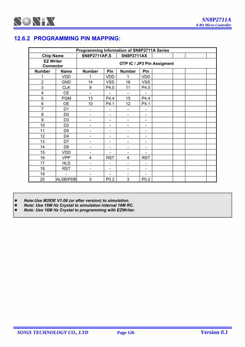
SN8P2711A 8-Bit Micro-Controller
SONiX TECHNOLOGY CO., LTD Page 126 Version 0.1
12.6.2 PROGRAMMING PIN MAPPING:
Programming Information of SN8P2711A Series Chip Name SN8P2711AP,S SN8P2711AX EZ Writer Connector OTP IC / JP3 Pin Assigment
Number Name Number Pin Number Pin 1 VDD 1 VDD 1 VDD 2 GND 14 VSS 16 VSS 3 CLK 9 P4.0 11 P4.0 4 CE - - - - 5 PGM 13 P4.4 15 P4.4 6 OE 10 P4.1 12 P4.1 7 D1 - - - - 8 D0 - - - - 9 D3 - - - - 10 D2 - - - - 11 D5 - - - - 12 D4 - - - - 13 D7 - - - - 14 D6 - - - - 15 VDD - - - - 16 VPP 4 RST 4 RST 17 HLS - - - - 18 RST - - - - 19 - - - - - 20 ALSB/PDB 3 P0.2 3 P0.2
Note:Use M2IDE V1.06 (or after version) to simulation. Note: Use 16M Hz Crystal to simulation internal 16M RC. Note: Use 16M Hz Crystal to programming with EZWriter.
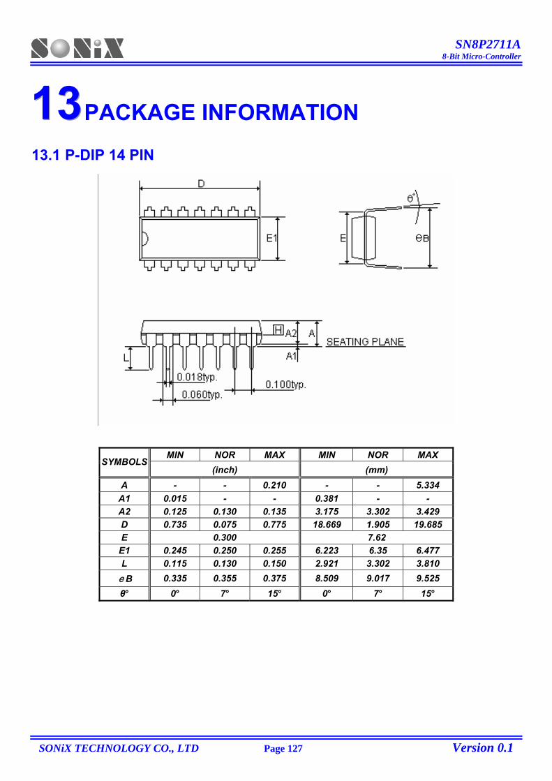
SN8P2711A 8-Bit Micro-Controller
SONiX TECHNOLOGY CO., LTD Page 127 Version 0.1
111333 PACKAGE INFORMATION
13.1 P-DIP 14 PIN
MIN NOR MAX MIN NOR MAX SYMBOLS
(inch) (mm) A - - 0.210 - - 5.334
A1 0.015 - - 0.381 - - A2 0.125 0.130 0.135 3.175 3.302 3.429 D 0.735 0.075 0.775 18.669 1.905 19.685 E 0.300 7.62
E1 0.245 0.250 0.255 6.223 6.35 6.477 L 0.115 0.130 0.150 2.921 3.302 3.810 eB 0.335 0.355 0.375 8.509 9.017 9.525 θ° 0° 7° 15° 0° 7° 15°
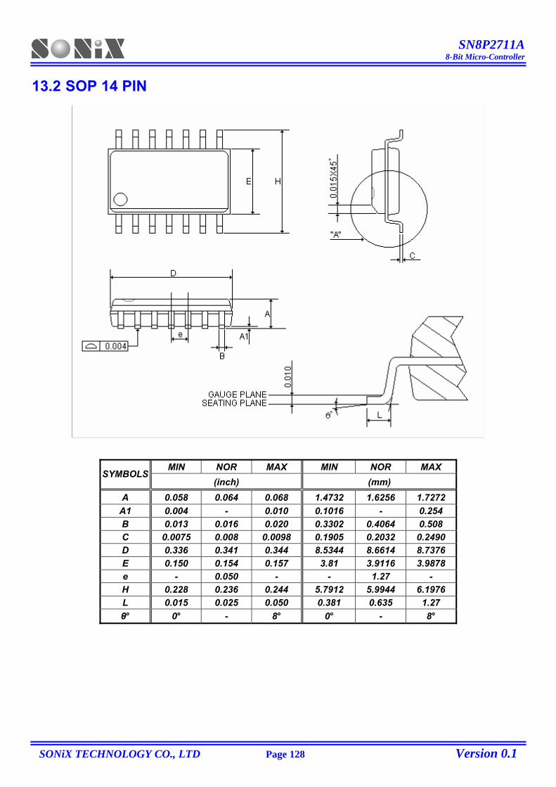
SN8P2711A 8-Bit Micro-Controller
SONiX TECHNOLOGY CO., LTD Page 128 Version 0.1
13.2 SOP 14 PIN
MIN NOR MAX MIN NOR MAX SYMBOLS
(inch) (mm) A 0.058 0.064 0.068 1.4732 1.6256 1.7272
A1 0.004 - 0.010 0.1016 - 0.254 B 0.013 0.016 0.020 0.3302 0.4064 0.508 C 0.0075 0.008 0.0098 0.1905 0.2032 0.2490 D 0.336 0.341 0.344 8.5344 8.6614 8.7376 E 0.150 0.154 0.157 3.81 3.9116 3.9878 e - 0.050 - - 1.27 - H 0.228 0.236 0.244 5.7912 5.9944 6.1976 L 0.015 0.025 0.050 0.381 0.635 1.27 θ° 0° - 8° 0° - 8°
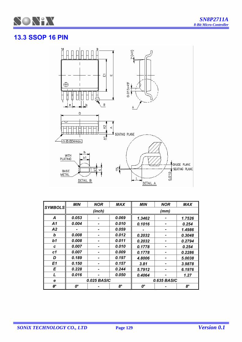
SN8P2711A 8-Bit Micro-Controller
SONiX TECHNOLOGY CO., LTD Page 129 Version 0.1
13.3 SSOP 16 PIN
MIN NOR MAX MIN NOR MAX SYMBOLS
(inch) (mm) A 0.053 - 0.069 1.3462 - 1.7526
A1 0.004 - 0.010 0.1016 - 0.254 A2 - - 0.059 - - 1.4986 b 0.008 - 0.012 0.2032 - 0.3048 b1 0.008 - 0.011 0.2032 - 0.2794 c 0.007 - 0.010 0.1778 - 0.254
c1 0.007 - 0.009 0.1778 - 0.2286 D 0.189 - 0.197 4.8006 - 5.0038 E1 0.150 - 0.157 3.81 - 3.9878 E 0.228 - 0.244 5.7912 - 6.1976 L 0.016 - 0.050 0.4064 - 1.27 e 0.025 BASIC 0.635 BASIC θ° 0° - 8° 0° - 8°
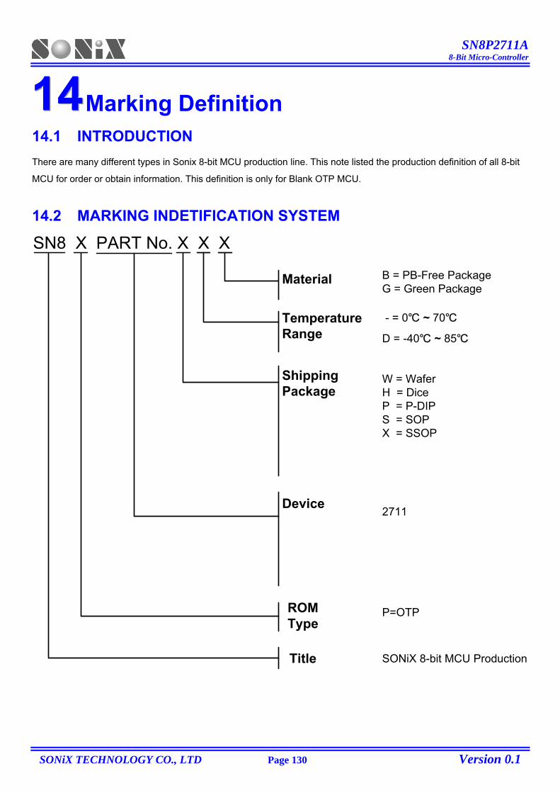
SN8P2711A 8-Bit Micro-Controller
SONiX TECHNOLOGY CO., LTD Page 130 Version 0.1
111444 Marking Definition 14.1 INTRODUCTION There are many different types in Sonix 8-bit MCU production line. This note listed the production definition of all 8-bit
MCU for order or obtain information. This definition is only for Blank OTP MCU.
14.2 MARKING INDETIFICATION SYSTEM
SN8 X PART No. X X X
Title SONiX 8-bit MCU Production
ROMType
P=OTP
Material B = PB-Free PackageG = Green Package
TemperatureRange
- = 0 ~ 70
D = -40 ~ 85
ShippingPackage
W = WaferH = DiceP = P-DIPS = SOPX = SSOP
Device 2711
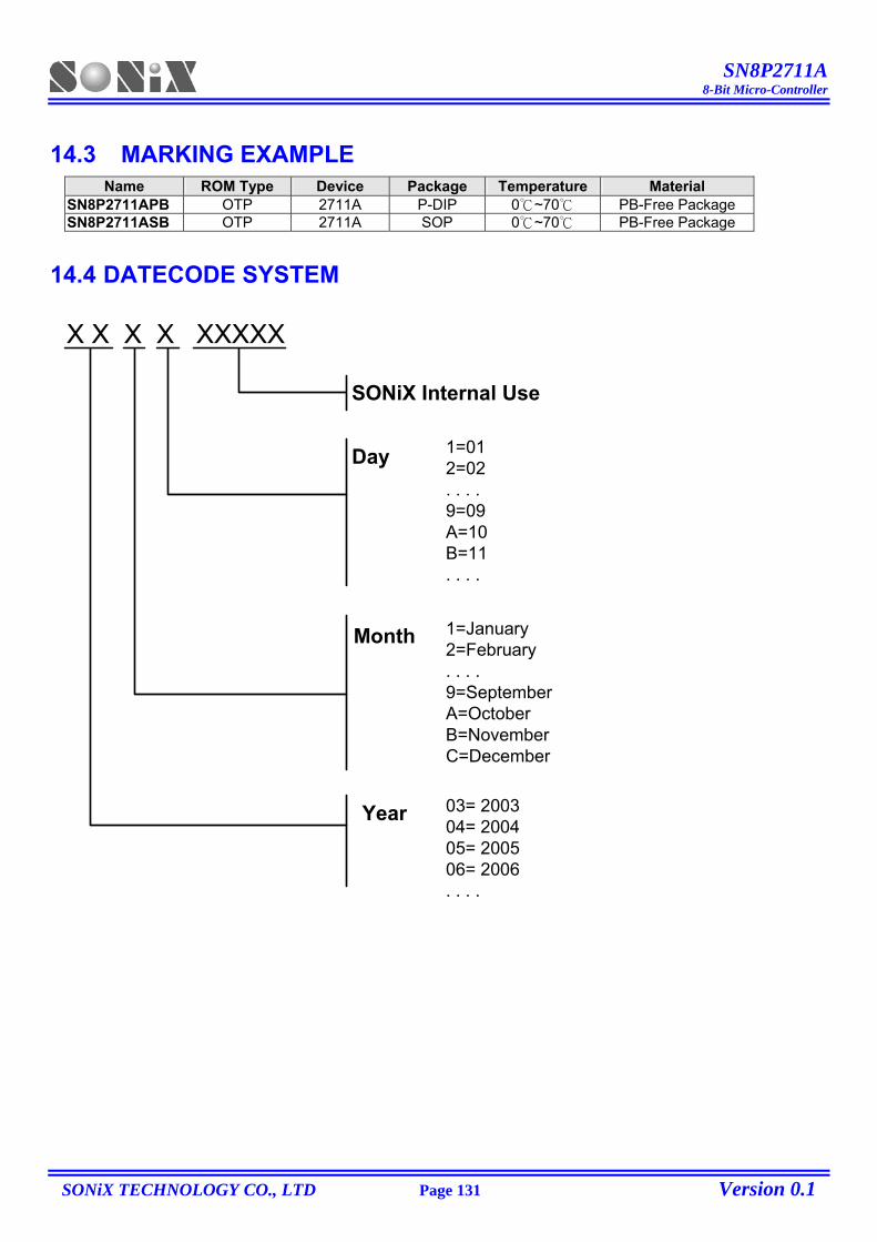
SN8P2711A 8-Bit Micro-Controller
SONiX TECHNOLOGY CO., LTD Page 131 Version 0.1
14.3 MARKING EXAMPLE Name ROM Type Device Package Temperature Material
SN8P2711APB OTP 2711A P-DIP 0 ~70 PB-Free Package SN8P2711ASB OTP 2711A SOP 0 ~70 PB-Free Package
14.4 DATECODE SYSTEM
X X X X XXXXX
Year
Month 1=January2=February. . . .9=SeptemberA=OctoberB=NovemberC=December
SONiX Internal Use
Day 1=012=02. . . .9=09A=10B=11. . . .
03= 200304= 200405= 200506= 2006. . . .
SN8P2711A 8-Bit Micro-Controller
SONiX TECHNOLOGY CO., LTD Page 132 Version 0.1
SONIX reserves the right to make change without further notice to any products herein to improve reliability, function or design. SONIX does not assume any liability arising out of the application or use of any product or circuit described herein; neither does it convey any license under its patent rights nor the rights of others. SONIX products are not designed, intended, or authorized for us as components in systems intended, for surgical implant into the body, or other applications intended to support or sustain life, or for any other application in which the failure of the SONIX product could create a situation where personal injury or death may occur. Should Buyer purchase or use SONIX products for any such unintended or unauthorized application. Buyer shall indemnify and hold SONIX and its officers , employees, subsidiaries, affiliates and distributors harmless against all claims, cost, damages, and expenses, and reasonable attorney fees arising out of, directly or indirectly, any claim of personal injury or death associated with such unintended or unauthorized use even if such claim alleges that SONIX was negligent regarding the design or manufacture of the part.
Main Office: Address: 9F, NO. 8, Hsien Cheng 5th St, Chupei City, Hsinchu, Taiwan R.O.C. Tel: 886-3-551 0520 Fax: 886-3-551 0523 Taipei Office: Address: 15F-2, NO. 171, Song Ted Road, Taipei, Taiwan R.O.C. Tel: 886-2-2759 1980 Fax: 886-2-2759 8180 Hong Kong Office: Unit No.705,Level 7 Tower 1,Grand Central Plaza 138 Shatin Rural Committee Road,Shatin,New Territories,Hong Kong. Tel: 852-2723-8086 Fax: 852-2723-9179 Technical Support by Email: [email protected]