Embed Size (px)
Citation preview

SN74HCS157-Q1 Automotive Quadruple 2-to-1 Multiplexer with Schmitt-Trigger Inputs
1 Features• AEC-Q100 Qualified for automotive applications:
– Device temperature grade 1: –40°C to +125°C,TA
– Device HBM ESD Classification Level 2– Device CDM ESD Classifcation Level C6
• Wide operating voltage range: 2 V to 6 V• Schmitt-trigger inputs allow for slow or noisy input
signals• Low power consumption
– Typical ICC of 100 nA– Typical input leakage current of ±100 nA
• ±7.8-mA output drive at 6 V
2 Applications• Data selection• Multiplexing
3 DescriptionThe SN74HCS157-Q1 contains four data selectors/multiplexers to select one of two data sources. Allchannels are controlled by the same address select(A/B) input, and strobe (G) input. A high level at thestrobe terminal forces all outputs low.
Device InformationPART NUMBER PACKAGE(1) BODY SIZE (NOM)
SN74HCS157PW-Q1 TSSOP (16) 5.00 mm × 4.40 mm
SN74HCS157D-Q1 SOIC (16) 9.90 mm × 3.90 mm
Input Voltage
Su
pp
ly C
urr
en
t
Schmitt-trigger
CMOS Input
Response
Waveforms
Standard
CMOS Input
Response
Waveforms
Input Voltage
Su
pp
ly C
urr
en
t
Inp
ut
Vo
lta
ge
Input Voltage Time
Cu
rre
nt
Ou
tpu
t Vo
lta
ge
Cu
rre
nt
Ou
tpu
t Vo
lta
ge
Inp
ut
Vo
lta
ge
Time
Cu
rre
nt
Ou
tpu
t Vo
lta
ge
Cu
rre
nt
Ou
tpu
t Vo
lta
ge
Inp
ut
Vo
lta
ge
Input Voltage
Waveforms
Low Power Noise Rejection Supports Slow Inputs
Time Time
Time Time
Benefits of Schmitt-trigger inputs
www.ti.comSN74HCS157-Q1
SCLS820 – AUGUST 2020
Copyright © 2020 Texas Instruments Incorporated Submit Document Feedback 1
Product Folder Links: SN74HCS157-Q1
SN74HCS157-Q1SCLS820 – AUGUST 2020
An IMPORTANT NOTICE at the end of this data sheet addresses availability, warranty, changes, use in safety-critical applications,intellectual property matters and other important disclaimers. PRODUCTION DATA.
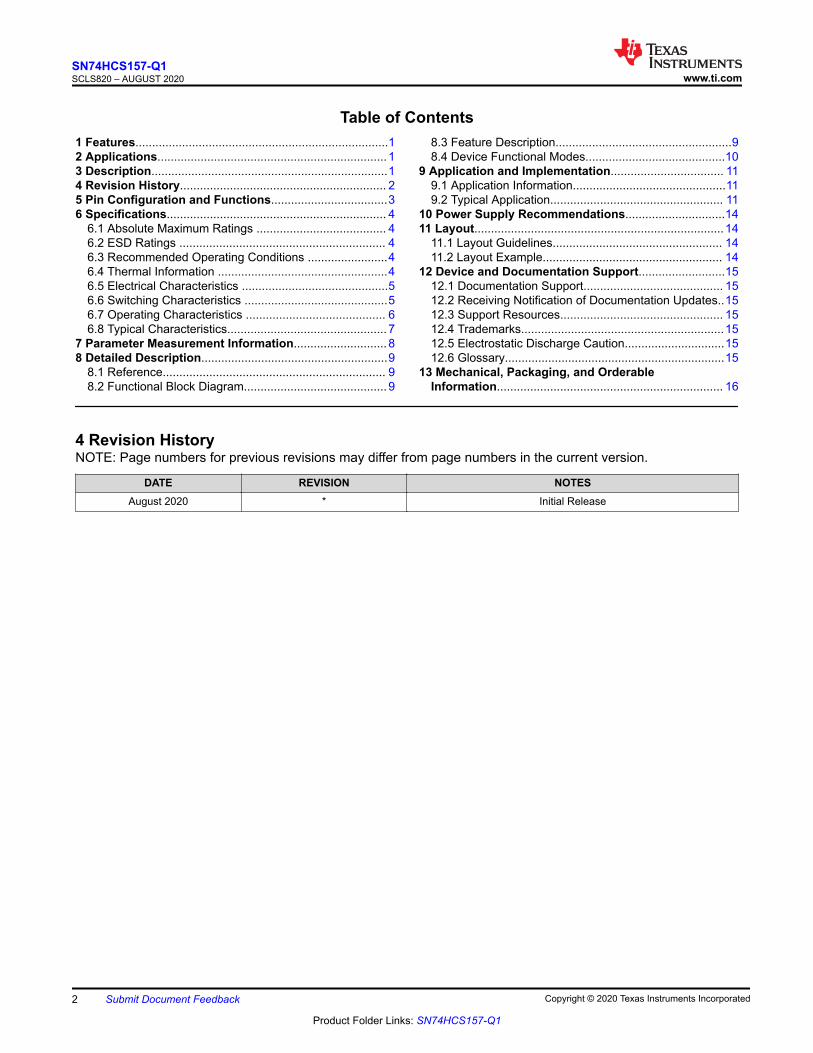
Table of Contents1 Features............................................................................12 Applications..................................................................... 13 Description.......................................................................14 Revision History.............................................................. 25 Pin Configuration and Functions...................................36 Specifications.................................................................. 4
6.1 Absolute Maximum Ratings ....................................... 46.2 ESD Ratings .............................................................. 46.3 Recommended Operating Conditions ........................46.4 Thermal Information ...................................................46.5 Electrical Characteristics ............................................56.6 Switching Characteristics ...........................................56.7 Operating Characteristics .......................................... 66.8 Typical Characteristics................................................ 7
7 Parameter Measurement Information............................ 88 Detailed Description........................................................9
8.1 Reference................................................................... 98.2 Functional Block Diagram........................................... 9
8.3 Feature Description.....................................................98.4 Device Functional Modes..........................................10
9 Application and Implementation.................................. 119.1 Application Information..............................................119.2 Typical Application.................................................... 11
10 Power Supply Recommendations..............................1411 Layout...........................................................................14
11.1 Layout Guidelines................................................... 1411.2 Layout Example...................................................... 14
12 Device and Documentation Support..........................1512.1 Documentation Support.......................................... 1512.2 Receiving Notification of Documentation Updates..1512.3 Support Resources................................................. 1512.4 Trademarks.............................................................1512.5 Electrostatic Discharge Caution..............................1512.6 Glossary..................................................................15
13 Mechanical, Packaging, and OrderableInformation.................................................................... 16
4 Revision HistoryNOTE: Page numbers for previous revisions may differ from page numbers in the current version.
DATE REVISION NOTESAugust 2020 * Initial Release
SN74HCS157-Q1SCLS820 – AUGUST 2020 www.ti.com
2 Submit Document Feedback Copyright © 2020 Texas Instruments Incorporated
Product Folder Links: SN74HCS157-Q1

5 Pin Configuration and Functions
1
2
3
7
4
5
6
14
13
12
8
11
10
9GND
4A
4Y
3A
VCC
15
16
1A
1B
1Y
2A
G
3Y
3B
4B
A/B
2B
2Y
D or PW Package 16-Pin SOIC or TSSOP Top View
Pin FunctionsPIN
I/O(1) DESCRIPTIONSOIC orTSSOP NO. NAME
1 A/B I Address select
2 1A I Channel 1, data input A
3 1B I Channel 1, data input B
4 1Y I Channel 1, data output
5 2A O Channel 2, data input A
6 2B O Channel 2, data input B
7 2Y I Channel 2, data output
8 GND — Ground
9 3Y I Channel 3, data output
10 3B I Channel 3, data input B
11 3A I Channel 3, data input A
12 4Y I Channel 4, data output
13 4B I Channel 4, data input B
14 4A I Channel 4, data input A
15 G I Output strobe, active low
16 VCC — Positive supply
www.ti.comSN74HCS157-Q1
SCLS820 – AUGUST 2020
Copyright © 2020 Texas Instruments Incorporated Submit Document Feedback 3
Product Folder Links: SN74HCS157-Q1
6 Specifications6.1 Absolute Maximum Ratingsover operating free-air temperature range (unless otherwise noted)(1)
MIN MAX UNITVCC Supply voltage –0.5 7 V
IIK Input clamp current(2) VI < –0.5 V or VI > VCC + 0.5 V ±20 mA
IOK Output clamp current(2) VI < –0.5 V or VI > VCC + 0.5 V ±20 mA
IO Continuous output current VO = 0 to VCC ±35 mA
Continuous current through VCC or GND ±70 mA
TJ Junction temperature(3) 150 °C
Tstg Storage temperature –65 150 °C
(1) Stresses beyond those listed under Absolute Maximum Rating may cause permanent damage to the device. These are stress ratingsonly, which do not imply functional operation of the device at these or any other conditions beyond those indicated underRecommended Operating Condition. Exposure to absolute-maximum-rated conditions for extended periods may affect devicereliability.
(2) The input and output voltage ratings may be exceeded if the input and output current ratings are observed.(3) Guaranteed by design.
6.2 ESD RatingsVALUE UNIT
V(ESD) Electrostatic discharge
Human body model (HBM), per AEC Q100-002(1)
HBM ESD Classification Level 2 ±4000V
Charged device model (CDM), per AECQ100-011 CDM ESD Classification Level C6 ±1500
(1) AEC Q100-002 indicate that HBM stressing shall be in accordance with the ANSI/ESDA/JEDEC JS-001 specification.
6.3 Recommended Operating Conditionsover operating free-air temperature range (unless otherwise noted)
MIN NOM MAX UNITVCC Supply voltage 2 5 6 V
VI Input voltage 0 VCC V
VO Output voltage 0 VCC V
TA Ambient temperature –40 125 °C
6.4 Thermal Information
THERMAL METRIC(1)
SN74HCS157-Q1UNITPW (TSSOP) D (SOIC)
16 PINS 16 PINSRθJA Junction-to-ambient thermal resistance 141.2 122.2 °C/W
RθJC(top) Junction-to-case (top) thermal resistance 78.8 80.9 °C/W
RθJB Junction-to-board thermal resistance 85.8 80.6 °C/W
ΨJT Junction-to-top characterization parameter 27.7 40.4 °C/W
ΨJB Junction-to-board characterization parameter 85.5 80.3 °C/W
RθJC(bot) Junction-to-case (bottom) thermal resistance N/A N/A °C/W
(1) For more information about traditional and new thermal metrics, see the Semiconductor and IC Package Thermal Metrics applicationreport.
SN74HCS157-Q1SCLS820 – AUGUST 2020 www.ti.com
4 Submit Document Feedback Copyright © 2020 Texas Instruments Incorporated
Product Folder Links: SN74HCS157-Q1

6.5 Electrical Characteristicsover operating free-air temperature range; typical values measured at TA = 25°C (unless otherwise noted).
PARAMETER TEST CONDITIONS VCC MIN TYP MAX UNIT
VT+ Positive switching threshold
2 V 0.7 1.5
V4.5 V 1.7 3.15
6 V 2.1 4.2
VT- Negative switching threshold
2 V 0.3 1.0
V4.5 V 0.9 2.2
6 V 1.2 3.0
ΔVT Hysteresis (VT+ - VT-)(1)
2 V 0.2 1.0
V4.5 V 0.4 1.4
6 V 0.6 1.6
VOH High-level output voltage VI = VIH or VIL
IOH = -20 µA 2 V to 6 V VCC – 0.1 VCC – 0.002
VIOH = -6 mA 4.5 V 4.0 4.3
IOH = -7.8 mA 6 V 5.4 5.75
VOL Low-level output voltage VI = VIH or VIL
IOL = 20 µA 2 V to 6 V 0.002 0.1
VIOL = 6 mA 4.5 V 0.18 0.30
IOL = 7.8 mA 6 V 0.22 0.33
II Input leakage current VI = VCC or 0 6 V ±100 ±1000 nA
ICC Supply current VI = VCC or 0, IO = 0 6 V 0.1 2 µA
Ci Input capacitance 2 V to 6 V 5 pF
(1) Guaranteed by design.
6.6 Switching CharacteristicsCL = 50 pF; over operating free-air temperature range (unless otherwise noted). See Parameter MeasurementInformation.
PARAMETER FROM TO VCC
Operating free-air temperature (TA)UNIT25°C –40°C to 125°C
MIN TYP MAX MIN TYP MAX
fmax Max switching frequency
2 V 6 5
MHz4.5 V 31 25
6 V 36 29
tpd Propagation delay
A or B Y
2 V 21 32 55
ns
4.5 V 8 12 19
6 V 7 11 16
A/B Y
2 V 21 32 57
4.5 V 8 12 20
6 V 7 11 16
G Y
2 V 22 33 53
4.5 V 9 14 18
6 V 8 12 15
tt Transition-time Any output
2 V 13 21
ns4.5 V 6 9
6 V 5 7
www.ti.comSN74HCS157-Q1
SCLS820 – AUGUST 2020
Copyright © 2020 Texas Instruments Incorporated Submit Document Feedback 5
Product Folder Links: SN74HCS157-Q1
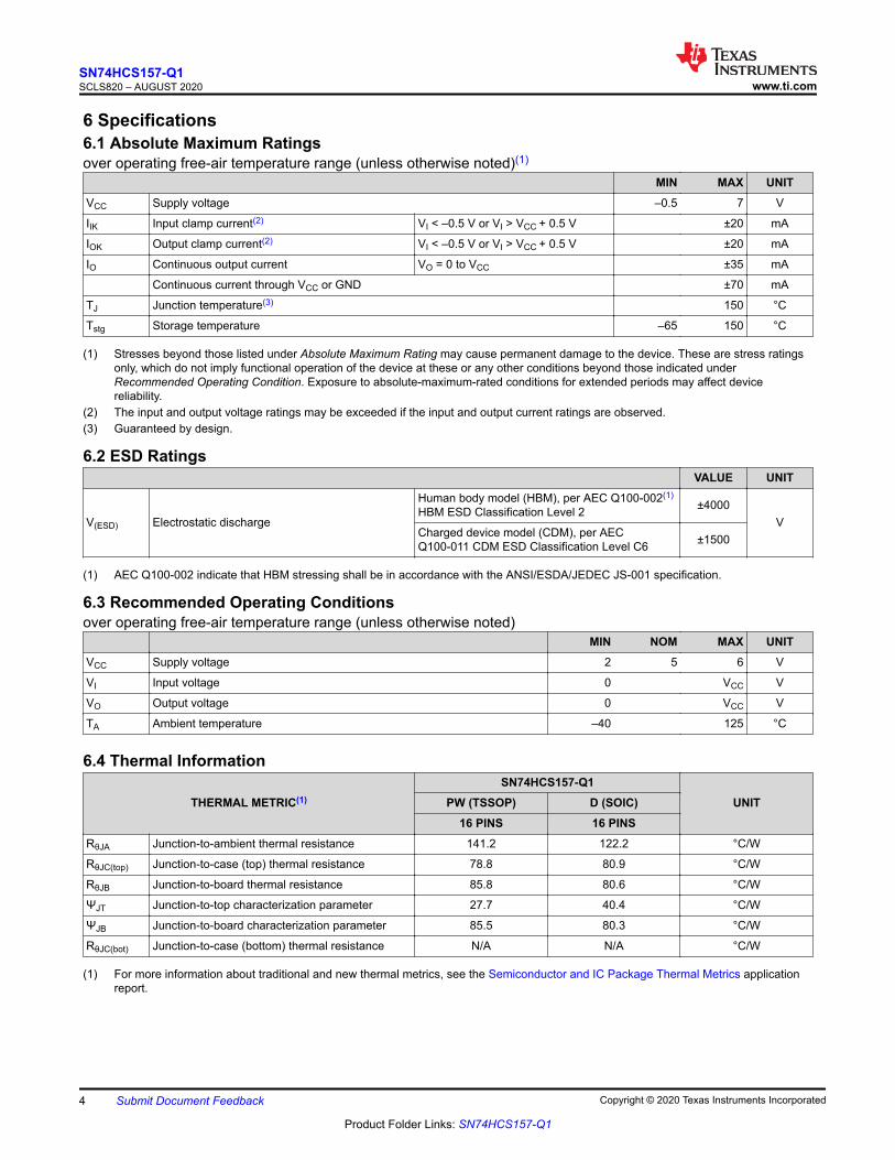
6.7 Operating Characteristicsover operating free-air temperature range; typical values measured at TA = 25°C (unless otherwise noted).
PARAMETER TEST CONDITIONS VCC MIN TYP MAX UNIT
CpdPower dissipation capacitanceper gate No load 2 V to 6 V 40 pF
SN74HCS157-Q1SCLS820 – AUGUST 2020 www.ti.com
6 Submit Document Feedback Copyright © 2020 Texas Instruments Incorporated
Product Folder Links: SN74HCS157-Q1

6.8 Typical CharacteristicsTA = 25°C
Output Sink Current (mA)
Outp
ut
Resis
tance (:
)
0 2.5 5 7.5 10 12.5 15 17.5 20 22.5 2526
28
30
32
34
36
38
40
42
44
46VCC = 2 VVCC = 3.3 VVCC = 4.5 VVCC = 6 V
Figure 6-1. Output driver resistance in LOW state.Output Source Current (mA)
Outp
ut
Resis
tance (:
)
0 2.5 5 7.5 10 12.5 15 17.5 20 22.5 2530
35
40
45
50
55
60
65
70VCC = 2 VVCC = 3.3 VVCC = 4.5 VVCC = 6 V
Figure 6-2. Output driver resistance in HIGH state.
VI ± Input Voltage (V)
I CC ±
Su
pp
ly C
urr
en
t (m
A)
0 0.5 1 1.5 2 2.5 3 3.50
0.02
0.04
0.06
0.08
0.1
0.12
0.14
0.16
0.18
0.2VCC = 2 V
VCC = 2.5 V
VCC = 3.3 V
Figure 6-3. Supply current across input voltage, 2-,2.5-, and 3.3-V supply
VI ± Input Voltage (V)
I CC ±
Su
pp
ly C
urr
en
t (m
A)
0 0.5 1 1.5 2 2.5 3 3.5 4 4.5 5 5.5 60
0.05
0.1
0.15
0.2
0.25
0.3
0.35
0.4
0.45
0.5
0.55
0.6
0.65VCC = 4.5 V
VCC = 5 V
VCC = 6 V
Figure 6-4. Supply current across input voltage,4.5-, 5-, and 6-V supply
www.ti.comSN74HCS157-Q1
SCLS820 – AUGUST 2020
Copyright © 2020 Texas Instruments Incorporated Submit Document Feedback 7
Product Folder Links: SN74HCS157-Q1
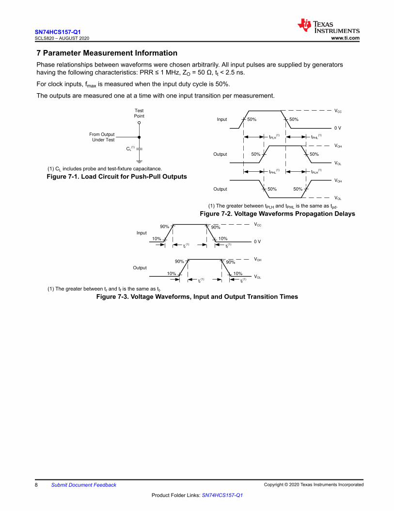
7 Parameter Measurement InformationPhase relationships between waveforms were chosen arbitrarily. All input pulses are supplied by generatorshaving the following characteristics: PRR ≤ 1 MHz, ZO = 50 Ω, tt < 2.5 ns.
For clock inputs, fmax is measured when the input duty cycle is 50%.
The outputs are measured one at a time with one input transition per measurement.
CL(1)
From Output
Under Test
Test
Point
(1) CL includes probe and test-fixture capacitance.Figure 7-1. Load Circuit for Push-Pull Outputs
50%Input 50%
VCC
0 V
50% 50%
VOH
VOL
tPLH(1) tPHL
(1)
VOH
VOL
tPHL(1) tPLH
(1)
Output
Output 50% 50%
(1) The greater between tPLH and tPHL is the same as tpd.Figure 7-2. Voltage Waveforms Propagation Delays
VOH
VOL
Output
VCC
0 V
Input
tf(1)tr
(1)
90%
10%
90%
10%
tr(1)
90%
10%
tf(1)
90%
10%
(1) The greater between tr and tf is the same as tt.Figure 7-3. Voltage Waveforms, Input and Output Transition Times
SN74HCS157-Q1SCLS820 – AUGUST 2020 www.ti.com
8 Submit Document Feedback Copyright © 2020 Texas Instruments Incorporated
Product Folder Links: SN74HCS157-Q1

8 Detailed Description8.1 ReferenceThe SN74HCS157-Q1 is a high speed silicon gate CMOS multiplexer well suited to multiplexing and data routingapplications. It contains four 2:1 multiplexers.
The SN74HCS157-Q1 operates asynchronously, with each Y output being equal to the input selected by theaddress input (A/B). All four channels are controlled by the same address input.
The strobe (G) input forces all Y outputs low, regardless of the state of other inputs.
All inputs include Schmitt-triggers allowing for slow input transitions and providing additional noise margin.
8.2 Functional Block Diagram
A/B
xA
xB
xY
G
Shared Control Logic
One of Four 2:1 Multiplexers
Figure 8-1. Logic Diagram (Positive Logic) for SN74HCS157-Q1
8.3 Feature Description8.3.1 Balanced CMOS Push-Pull Outputs
This device includes balanced CMOS push-pull outputs. The term "balanced" indicates that the device can sinkand source similar currents. The drive capability of this device may create fast edges into light loads so routingand load conditions should be considered to prevent ringing. Additionally, the outputs of this device are capableof driving larger currents than the device can sustain without being damaged. It is important for the output powerof the device to be limited to avoid damage due to overcurrent. The electrical and thermal limits defined in theAbsolute Maximum Ratings must be followed at all times.
Unused push-pull CMOS outputs should be left disconnected.
8.3.2 CMOS Schmitt-Trigger Inputs
This device includes inputs with the Schmitt-trigger architecture. These inputs are high impedance and aretypically modeled as a resistor in parallel with the input capacitance given in the Electrical Characteristics tablefrom the input to ground. The worst case resistance is calculated with the maximum input voltage, given in theAbsolute Maximum Ratings table, and the maximum input leakage current, given in the Electrical Characteristicstable, using Ohm's law (R = V ÷ I).
The Schmitt-trigger input architecture provides hysteresis as defined by ΔVT in the Electrical Characteristicstable, which makes this device extremely tolerant to slow or noisy inputs. While the inputs can be driven muchslower than standard CMOS inputs, it is still recommended to properly terminate unused inputs. Driving the
www.ti.comSN74HCS157-Q1
SCLS820 – AUGUST 2020
Copyright © 2020 Texas Instruments Incorporated Submit Document Feedback 9
Product Folder Links: SN74HCS157-Q1

inputs with slow transitioning signals will increase dynamic current consumption of the device. For additionalinformation regarding Schmitt-trigger inputs, please see Understanding Schmitt Triggers.
8.3.3 Clamp Diode Structure
The inputs and outputs to this device have both positive and negative clamping diodes as depicted in ElectricalPlacement of Clamping Diodes for Each Input and Output.
CAUTION
Voltages beyond the values specified in the Absolute Maximum Ratings table can cause damage tothe device. The input and output voltage ratings may be exceeded if the input and output clamp-current ratings are observed.
GND
LogicInput Output
VCCDevice
-IIK
+IIK +IOK
-IOK
Figure 8-2. Electrical Placement of Clamping Diodes for Each Input and Output
8.4 Device Functional ModesFunction Table lists the functional modes of the SN74HCS157-Q1.
Table 8-1. Function TableINPUTS(1)
OUTPUTG
SELECT DATAA/B A B Y
H X X X LL L L X LL L H X HL H X L LL H X H H
(1) H = High Voltage Level, L = Low Voltage Level, X = Don't Care
SN74HCS157-Q1SCLS820 – AUGUST 2020 www.ti.com
10 Submit Document Feedback Copyright © 2020 Texas Instruments Incorporated
Product Folder Links: SN74HCS157-Q1

9 Application and ImplementationNote
Information in the following applications sections is not part of the TI component specification, and TIdoes not warrant its accuracy or completeness. TI’s customers are responsible for determiningsuitability of components for their purposes. Customers should validate and test their designimplementation to confirm system functionality.
9.1 Application InformationThe SN74HCS157-Q1 is a quadruple 2-to-1 data selector/multiplexer. This application shows an example ofusing the device with all required connections to switch a 4-bit data bus between two source devices.
9.2 Typical Application
System
Controller
A/B
G
GND
2:1
Mux1B
1A
Device 0
Device 1
VCC
0.1F
4Y
VCC
D0A
D0B
D0C
D0D
D1A
D1B
D1C
D1D
DXA
DXB2:1
Mux
2:1
Mux
2:1
Mux
2B
2A
3B
3A
4B
4A
3Y
2Y
1Y
DXC
DXD
D0A
D0B
D0C
D0D
D1A
D1B
D1C
D1D
Figure 9-1. Typical application block diagram
9.2.1 Design Requirements9.2.1.1 Power Considerations
Ensure the desired supply voltage is within the range specified in the Recommended Operating Conditions. Thesupply voltage sets the device's electrical characteristics as described in the Electrical Characteristics.
The positive voltage supply must be capable of sourcing current equal to the total current to be sourced by alloutputs of the SN74HCS157-Q1 plus the maximum static supply current, ICC, listed in Electrical Characteristicsand any transient current required for switching. The logic device can only source as much current as is providedby the positive supply source. Be sure not to exceed the maximum total current through VCC listed in theAbsolute Maximum Ratings.
The ground must be capable of sinking current equal to the total current to be sunk by all outputs of theSN74HCS157-Q1 plus the maximum supply current, ICC, listed in Electrical Characteristics, and any transientcurrent required for switching. The logic device can only sink as much current as can be sunk into its groundconnection. Be sure not to exceed the maximum total current through GND listed in the Absolute MaximumRatings.
The SN74HCS157-Q1 can drive a load with a total capacitance less than or equal to 50 pF while still meeting allof the datasheet specifications. Larger capacitive loads can be applied, however it is not recommended toexceed 50 pF.
The SN74HCS157-Q1 can drive a load with total resistance described by RL ≥ VO / IO, with the output voltageand current defined in the Electrical Characteristics table with VOH and VOL. When outputting in the high state,the output voltage in the equation is defined as the difference between the measured output voltage and thesupply voltage at the VCC pin.
www.ti.comSN74HCS157-Q1
SCLS820 – AUGUST 2020
Copyright © 2020 Texas Instruments Incorporated Submit Document Feedback 11
Product Folder Links: SN74HCS157-Q1
Total power consumption can be calculated using the information provided in CMOS Power Consumption andCpd Calculation.
Thermal increase can be calculated using the information provided in Thermal Characteristics of Standard Linearand Logic (SLL) Packages and Devices.
CAUTION
The maximum junction temperature, TJ(max) listed in the Absolute Maximum Ratings, is an additionallimitation to prevent damage to the device. Do not violate any values listed in the Absolute MaximumRatings. These limits are provided to prevent damage to the device.
9.2.1.2 Input Considerations
Input signals must cross Vt-(min) to be considered a logic LOW, and Vt+(max) to be considered a logic HIGH. Donot exceed the maximum input voltage range found in the Absolute Maximum Ratings.
Unused inputs must be terminated to either VCC or ground. These can be directly terminated if the input iscompletely unused, or they can be connected with a pull-up or pull-down resistor if the input is to be usedsometimes, but not always. A pull-up resistor is used for a default state of HIGH, and a pull-down resistor is usedfor a default state of LOW. The resistor size is limited by drive current of the controller, leakage current into theSN74HCS157-Q1, as specified in the Electrical Characteristics, and the desired input transition rate. A 10-kΩresistor value is often used due to these factors.
The SN74HCS157-Q1 has no input signal transition rate requirements because it has Schmitt-trigger inputs.
Another benefit to having Schmitt-trigger inputs is the ability to reject noise. Noise with a large enough amplitudecan still cause issues. To know how much noise is too much, please refer to the ΔVT(min) in the ElectricalCharacteristics. This hysteresis value will provide the peak-to-peak limit.
Unlike what happens with standard CMOS inputs, Schmitt-trigger inputs can be held at any valid value withoutcausing huge increases in power consumption. The typical additional current caused by holding an input at avalue other than VCC or ground is plotted in the Typical Characteristics.
Refer to the Feature Description section for additional information regarding the inputs for this device.
9.2.1.3 Output Considerations
The positive supply voltage is used to produce the output HIGH voltage. Drawing current from the output willdecrease the output voltage as specified by the VOH specification in the Electrical Characteristics. The groundvoltage is used to produce the output LOW voltage. Sinking current into the output will increase the outputvoltage as specified by the VOL specification in the Electrical Characteristics.
Push-pull outputs that could be in opposite states, even for a very short time period, should never be connecteddirectly together. This can cause excessive current and damage to the device.
Two channels within the same device with the same input signals can be connected in parallel for additionaloutput drive strength.
Unused outputs can be left floating. Do not connect outputs directly to VCC or ground.
Refer to Feature Description section for additional information regarding the outputs for this device.
9.2.2 Detailed Design Procedure
1. Add a decoupling capacitor from VCC to GND. The capacitor needs to be placed physically close to thedevice and electrically close to both the VCC and GND pins. An example layout is shown in the Layoutsection.
2. Ensure the capacitive load at the output is ≤ 50 pF. This is not a hard limit, however it will ensure optimalperformance. This can be accomplished by providing short, appropriately sized traces from theSN74HCS157-Q1 to the receiving device(s).
SN74HCS157-Q1SCLS820 – AUGUST 2020 www.ti.com
12 Submit Document Feedback Copyright © 2020 Texas Instruments Incorporated
Product Folder Links: SN74HCS157-Q1

3. Ensure the resistive load at the output is larger than (VCC / IO(max)) Ω. This will ensure that the maximumoutput current from the Absolute Maximum Ratings is not violated. Most CMOS inputs have a resistive loadmeasured in megaohms; much larger than the minimum calculated above.
4. Thermal issues are rarely a concern for logic gates, however the power consumption and thermal increasecan be calculated using the steps provided in the application report, CMOS Power Consumption and CpdCalculation.
9.2.3 Application Curve
A/B
G
xY
xA
xB
Figure 9-2. Application timing diagram
www.ti.comSN74HCS157-Q1
SCLS820 – AUGUST 2020
Copyright © 2020 Texas Instruments Incorporated Submit Document Feedback 13
Product Folder Links: SN74HCS157-Q1

10 Power Supply RecommendationsThe power supply can be any voltage between the minimum and maximum supply voltage rating located in theRecommended Operating Conditions. Each VCC terminal should have a good bypass capacitor to prevent powerdisturbance. A 0.1-μF capacitor is recommended for this device. It is acceptable to parallel multiple bypass capsto reject different frequencies of noise. The 0.1-μF and 1-μF capacitors are commonly used in parallel. Thebypass capacitor should be installed as close to the power terminal as possible for best results, as shown ingiven example layout image.
11 Layout11.1 Layout GuidelinesWhen using multiple-input and multiple-channel logic devices inputs must not ever be left floating. In manycases, functions or parts of functions of digital logic devices are unused; for example, when only two inputs of atriple-input AND gate are used or only 3 of the 4 buffer gates are used. Such unused input pins must not be leftunconnected because the undefined voltages at the outside connections result in undefined operational states.All unused inputs of digital logic devices must be connected to a logic high or logic low voltage, as defined by theinput voltage specifications, to prevent them from floating. The logic level that must be applied to any particularunused input depends on the function of the device. Generally, the inputs are tied to GND or VCC, whichevermakes more sense for the logic function or is more convenient.
11.2 Layout Example
1
2
3
4
5
6
7
16
15
14
13
12
11
10
GND VCC
0.1 F
Bypass capacitor
placed close to the
device
Avoid 90°
corners for
signal lines
Recommend GND flood fill for
improved signal isolation, noise
reduction, and thermal dissipation
Unused output
left floating8 9
A/B
1A
1B
1Y
2A
2B
2Y
GND
VCC
G
4A
4B
4Y
3A
3B
3Y
Unused inputs
tied to VCC
Figure 11-1. Example layout for the SN74HCS157-Q1.
SN74HCS157-Q1SCLS820 – AUGUST 2020 www.ti.com
14 Submit Document Feedback Copyright © 2020 Texas Instruments Incorporated
Product Folder Links: SN74HCS157-Q1
12 Device and Documentation SupportTI offers an extensive line of development tools. Tools and software to evaluate the performance of the device,generate code, and develop solutions are listed below.
12.1 Documentation Support12.1.1 Related Documentation
For related documentation see the following:
• Texas Instruments, HCMOS Design Considerations application report (SCLA007)• Texas Instruments, CMOS Power Consumption and Cpd Calculation application report (SDYA009)• Texas Instruments, Designing With Logic application report
12.2 Receiving Notification of Documentation UpdatesTo receive notification of documentation updates, navigate to the device product folder on ti.com. Click onSubscribe to updates to register and receive a weekly digest of any product information that has changed. Forchange details, review the revision history included in any revised document.
12.3 Support ResourcesTI E2E™ support forums are an engineer's go-to source for fast, verified answers and design help — straightfrom the experts. Search existing answers or ask your own question to get the quick design help you need.
Linked content is provided "AS IS" by the respective contributors. They do not constitute TI specifications and donot necessarily reflect TI's views; see TI's Terms of Use.
12.4 TrademarksTI E2E™ is a trademark of Texas Instruments.All other trademarks are the property of their respective owners.12.5 Electrostatic Discharge Caution
This integrated circuit can be damaged by ESD. Texas Instruments recommends that all integrated circuits be handledwith appropriate precautions. Failure to observe proper handling and installation procedures can cause damage.ESD damage can range from subtle performance degradation to complete device failure. Precision integrated circuits maybe more susceptible to damage because very small parametric changes could cause the device not to meet its publishedspecifications.
12.6 GlossaryTI Glossary This glossary lists and explains terms, acronyms, and definitions.
www.ti.comSN74HCS157-Q1
SCLS820 – AUGUST 2020
Copyright © 2020 Texas Instruments Incorporated Submit Document Feedback 15
Product Folder Links: SN74HCS157-Q1
13 Mechanical, Packaging, and Orderable InformationThe following pages include mechanical, packaging, and orderable information. This information is the mostcurrent data available for the designated devices. This data is subject to change without notice and revision ofthis document. For browser-based versions of this data sheet, refer to the left-hand navigation.
SN74HCS157-Q1SCLS820 – AUGUST 2020 www.ti.com
16 Submit Document Feedback Copyright © 2020 Texas Instruments Incorporated
Product Folder Links: SN74HCS157-Q1
PACKAGE OPTION ADDENDUM
www.ti.com 4-Feb-2021
Addendum-Page 1
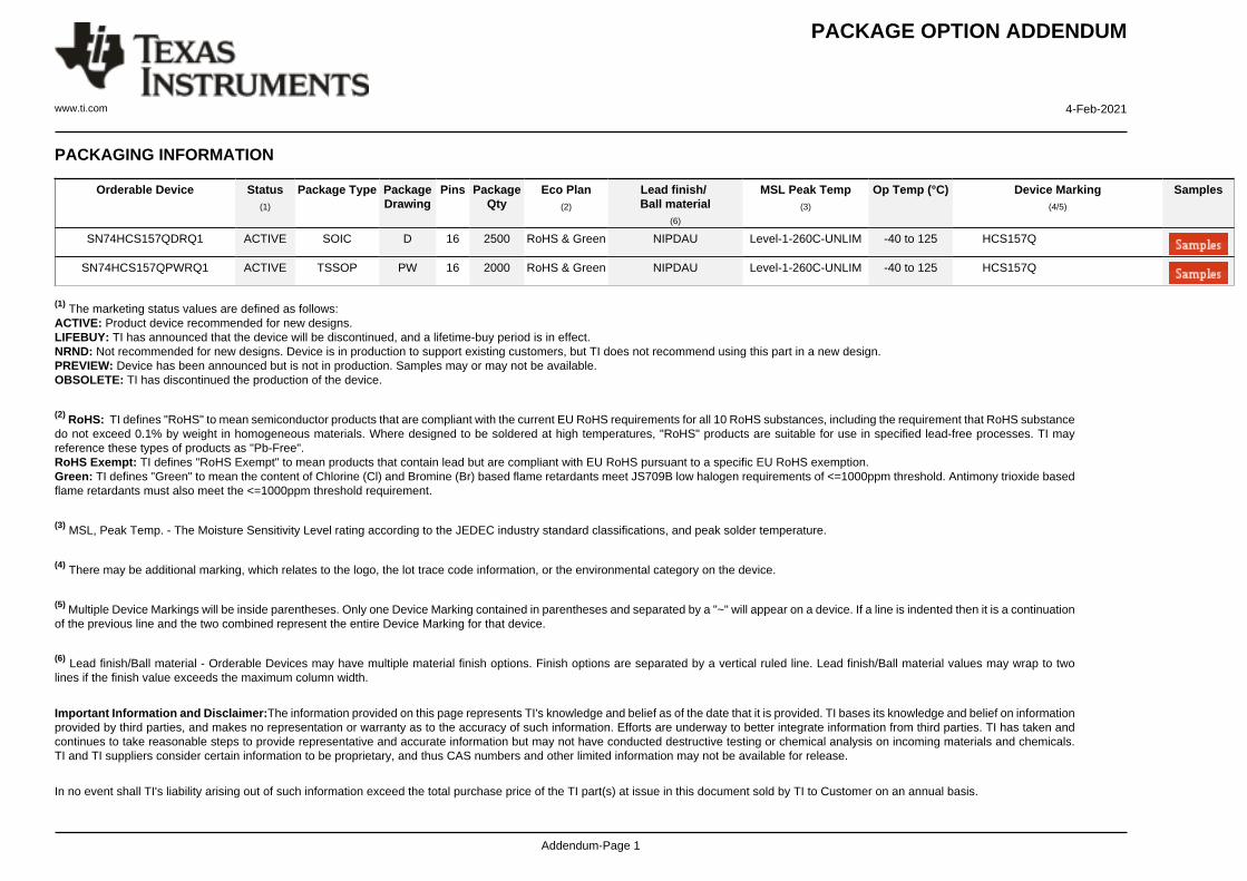
PACKAGING INFORMATION
Orderable Device Status(1)
Package Type PackageDrawing
Pins PackageQty
Eco Plan(2)
Lead finish/Ball material
(6)
MSL Peak Temp(3)
Op Temp (°C) Device Marking(4/5)
Samples
SN74HCS157QDRQ1 ACTIVE SOIC D 16 2500 RoHS & Green NIPDAU Level-1-260C-UNLIM -40 to 125 HCS157Q
SN74HCS157QPWRQ1 ACTIVE TSSOP PW 16 2000 RoHS & Green NIPDAU Level-1-260C-UNLIM -40 to 125 HCS157Q
(1) The marketing status values are defined as follows:ACTIVE: Product device recommended for new designs.LIFEBUY: TI has announced that the device will be discontinued, and a lifetime-buy period is in effect.NRND: Not recommended for new designs. Device is in production to support existing customers, but TI does not recommend using this part in a new design.PREVIEW: Device has been announced but is not in production. Samples may or may not be available.OBSOLETE: TI has discontinued the production of the device.
(2) RoHS: TI defines "RoHS" to mean semiconductor products that are compliant with the current EU RoHS requirements for all 10 RoHS substances, including the requirement that RoHS substancedo not exceed 0.1% by weight in homogeneous materials. Where designed to be soldered at high temperatures, "RoHS" products are suitable for use in specified lead-free processes. TI mayreference these types of products as "Pb-Free".RoHS Exempt: TI defines "RoHS Exempt" to mean products that contain lead but are compliant with EU RoHS pursuant to a specific EU RoHS exemption.Green: TI defines "Green" to mean the content of Chlorine (Cl) and Bromine (Br) based flame retardants meet JS709B low halogen requirements of <=1000ppm threshold. Antimony trioxide basedflame retardants must also meet the <=1000ppm threshold requirement.
(3) MSL, Peak Temp. - The Moisture Sensitivity Level rating according to the JEDEC industry standard classifications, and peak solder temperature.
(4) There may be additional marking, which relates to the logo, the lot trace code information, or the environmental category on the device.
(5) Multiple Device Markings will be inside parentheses. Only one Device Marking contained in parentheses and separated by a "~" will appear on a device. If a line is indented then it is a continuationof the previous line and the two combined represent the entire Device Marking for that device.
(6) Lead finish/Ball material - Orderable Devices may have multiple material finish options. Finish options are separated by a vertical ruled line. Lead finish/Ball material values may wrap to twolines if the finish value exceeds the maximum column width.
Important Information and Disclaimer:The information provided on this page represents TI's knowledge and belief as of the date that it is provided. TI bases its knowledge and belief on informationprovided by third parties, and makes no representation or warranty as to the accuracy of such information. Efforts are underway to better integrate information from third parties. TI has taken andcontinues to take reasonable steps to provide representative and accurate information but may not have conducted destructive testing or chemical analysis on incoming materials and chemicals.TI and TI suppliers consider certain information to be proprietary, and thus CAS numbers and other limited information may not be available for release.
In no event shall TI's liability arising out of such information exceed the total purchase price of the TI part(s) at issue in this document sold by TI to Customer on an annual basis.

PACKAGE OPTION ADDENDUM
www.ti.com 4-Feb-2021
Addendum-Page 2
OTHER QUALIFIED VERSIONS OF SN74HCS157-Q1 :
• Catalog: SN74HCS157
NOTE: Qualified Version Definitions:
• Catalog - TI's standard catalog product

TAPE AND REEL INFORMATION
*All dimensions are nominal
Device PackageType
PackageDrawing
Pins SPQ ReelDiameter
(mm)
ReelWidth
W1 (mm)
A0(mm)
B0(mm)
K0(mm)
P1(mm)
W(mm)
Pin1Quadrant
SN74HCS157QDRQ1 SOIC D 16 2500 330.0 16.4 6.5 10.3 2.1 8.0 16.0 Q1
SN74HCS157QPWRQ1 TSSOP PW 16 2000 330.0 12.4 6.9 5.6 1.6 8.0 12.0 Q1
PACKAGE MATERIALS INFORMATION
www.ti.com 4-Feb-2021
Pack Materials-Page 1

*All dimensions are nominal
Device Package Type Package Drawing Pins SPQ Length (mm) Width (mm) Height (mm)
SN74HCS157QDRQ1 SOIC D 16 2500 853.0 449.0 35.0
SN74HCS157QPWRQ1 TSSOP PW 16 2000 853.0 449.0 35.0
PACKAGE MATERIALS INFORMATION
www.ti.com 4-Feb-2021
Pack Materials-Page 2


www.ti.com
PACKAGE OUTLINE
C
14X 0.65
2X4.55
16X 0.300.19
TYP6.66.2
1.2 MAX
0.150.05
0.25GAGE PLANE
-80
BNOTE 4
4.54.3
A
NOTE 3
5.14.9
0.750.50
(0.15) TYP
TSSOP - 1.2 mm max heightPW0016ASMALL OUTLINE PACKAGE
4220204/A 02/2017
1
89
16
0.1 C A B
PIN 1 INDEX AREA
SEE DETAIL A
0.1 C
NOTES: 1. All linear dimensions are in millimeters. Any dimensions in parenthesis are for reference only. Dimensioning and tolerancing per ASME Y14.5M. 2. This drawing is subject to change without notice. 3. This dimension does not include mold flash, protrusions, or gate burrs. Mold flash, protrusions, or gate burrs shall not exceed 0.15 mm per side. 4. This dimension does not include interlead flash. Interlead flash shall not exceed 0.25 mm per side.5. Reference JEDEC registration MO-153.
SEATINGPLANE
A 20DETAIL ATYPICAL
SCALE 2.500

www.ti.com
EXAMPLE BOARD LAYOUT
0.05 MAXALL AROUND
0.05 MINALL AROUND
16X (1.5)
16X (0.45)
14X (0.65)
(5.8)
(R0.05) TYP
TSSOP - 1.2 mm max heightPW0016ASMALL OUTLINE PACKAGE
4220204/A 02/2017
NOTES: (continued) 6. Publication IPC-7351 may have alternate designs. 7. Solder mask tolerances between and around signal pads can vary based on board fabrication site.
LAND PATTERN EXAMPLEEXPOSED METAL SHOWN
SCALE: 10X
SYMM
SYMM
1
8 9
16
15.000
METALSOLDER MASKOPENING
METAL UNDERSOLDER MASK
SOLDER MASKOPENING
EXPOSED METALEXPOSED METAL
SOLDER MASK DETAILS
NON-SOLDER MASKDEFINED
(PREFERRED)
SOLDER MASKDEFINED

www.ti.com
EXAMPLE STENCIL DESIGN
16X (1.5)
16X (0.45)
14X (0.65)
(5.8)
(R0.05) TYP
TSSOP - 1.2 mm max heightPW0016ASMALL OUTLINE PACKAGE
4220204/A 02/2017
NOTES: (continued) 8. Laser cutting apertures with trapezoidal walls and rounded corners may offer better paste release. IPC-7525 may have alternate design recommendations. 9. Board assembly site may have different recommendations for stencil design.
SOLDER PASTE EXAMPLEBASED ON 0.125 mm THICK STENCIL
SCALE: 10X
SYMM
SYMM
1
8 9
16
IMPORTANT NOTICE AND DISCLAIMERTI PROVIDES TECHNICAL AND RELIABILITY DATA (INCLUDING DATASHEETS), DESIGN RESOURCES (INCLUDING REFERENCEDESIGNS), APPLICATION OR OTHER DESIGN ADVICE, WEB TOOLS, SAFETY INFORMATION, AND OTHER RESOURCES “AS IS”AND WITH ALL FAULTS, AND DISCLAIMS ALL WARRANTIES, EXPRESS AND IMPLIED, INCLUDING WITHOUT LIMITATION ANYIMPLIED WARRANTIES OF MERCHANTABILITY, FITNESS FOR A PARTICULAR PURPOSE OR NON-INFRINGEMENT OF THIRDPARTY INTELLECTUAL PROPERTY RIGHTS.These resources are intended for skilled developers designing with TI products. You are solely responsible for (1) selecting the appropriateTI products for your application, (2) designing, validating and testing your application, and (3) ensuring your application meets applicablestandards, and any other safety, security, or other requirements. These resources are subject to change without notice. TI grants youpermission to use these resources only for development of an application that uses the TI products described in the resource. Otherreproduction and display of these resources is prohibited. No license is granted to any other TI intellectual property right or to any third partyintellectual property right. TI disclaims responsibility for, and you will fully indemnify TI and its representatives against, any claims, damages,costs, losses, and liabilities arising out of your use of these resources.TI’s products are provided subject to TI’s Terms of Sale (https:www.ti.com/legal/termsofsale.html) or other applicable terms available eitheron ti.com or provided in conjunction with such TI products. TI’s provision of these resources does not expand or otherwise alter TI’sapplicable warranties or warranty disclaimers for TI products.IMPORTANT NOTICE
Mailing Address: Texas Instruments, Post Office Box 655303, Dallas, Texas 75265Copyright © 2021, Texas Instruments Incorporated