Embed Size (px)
Citation preview

SICOMP Industrial Microcomputer
(4)J31069-D2085-U001-A2-7618
Technical DescriptionOrder No.: 6AR1930-0AA07-2CA0 February 2001
SMP16-CPU06x
SMP16-CPU065, SMP16-CPU066
SMP16-AT CPU Boards with Pentium II/III Processor

SMP16-CPU06x
©Siemens AG 2001, All Rights Reserved2 (4)J31069-D2085-U001-A2-7618
List of changes to the technical description
Release 1)Overview of Changes Date of
Release
A0 First edition 11/99
A1 Addition of KS02 functions 07/00
A2 Addition of the SMP16-CPU066 02/01
1 Is the 4th block of digits of the drawing number in the footer
Explanation of the notation
* / # An asterisk or a pound character behind the name of a signal indicates a low-active signal(e.g., IOR* / FRAME#).
/ A slash between two signal names separates two level-dependent functions of a signal.(Example: C/D* means high level for a "command" and low level for "data").
– Connections indicated with a dash in a plug connector allocation table (bus or I/O interface)are reserved.
Signal Special signals not included in the specifications are shown in bold type in the signalallocation tables and then explained at the end (e.g., NMI).
Notes:SICOMP® is a registered brand of Siemens AG.IBM AT® and IBM PC® are registered brands of International Business Machines Corp.INTEL® is a registered brand of INTEL Corp.MS-DOS®, Windows® and Windows NT® are registered brands of Microsoft.All other designations in this documentation may be brands whose use by third parties for their own purposes may violate therights of the owner.
Passing on and duplication of this document as well as use and revelation of its contents is not permitted without expresspermission. Violators will be subject to damage claims. All rights reserved, particularly in the event a patent is granted or a utilitymodel is registered.With respect to freedom from rights of third parties, no liability is assumed for the specified circuits, descriptions and tables.Technical descriptions specify products but do not guarantee characteristics. The product described in this documentation mayrequire licensing. Please check with your Siemens office.Subject to delivery capacity and technical changes without prior notice TD1/Ka/WW8.0/VS5.0/A4

SMP16-CPU06x
©Siemens AG 2001, All Rights Reserved(4)J31069-D2085-U001-A2-7618 3
Notes on safety for SICOMP boards
Qualified personnel
A device may only be commissioned and operated by qualified personnel. For the purposes of thesafety notes in this manual, qualified personnel are persons who are authorized to commission,ground and tag devices, systems and electrical circuits in accordance with safety standards.
ESD protective measures
Caution
Always adhere to ESD (E lectrostatic Sensitive Device) guidelines when handling boardsand other componentsmarked with this symbol.
• Never touch the boards unless necessary work makes this unavoidable.
• When handling the boards, use a conductive and grounded work surface.
• Wear a grounding bracelet.
• Never touch chip pins, component connections or circuit board conductors when handling the boards.
• Never allow boards or components to touch chargeable objects (plastics).
• Never place components or boards in the vicinity of cathode ray tube units or television sets (minimumdistance: 10 cm).
• Leave the boards in their special packaging until you are ready to use them. Do not take the boards out oftheir packaging or touch them when registering them and so on.
• Boards may only be installed or removed when the power is off.
Wiring of bus backplanes
System-related signal wiring is done with wrap connections for SICOMP board systems. The powersupply cables are plug-in or screw-type connections which are bundled together with cable binders.
AttentionKeep all signal wiring (particularly the interrupt signal lines) as short as possible. If long signal cablescannot be avoided, use twisted pair wiring.
Related SICOMP literature
See the SICOMP IMC system manual for more information on installing and handling SICOMPboards.

SMP16-CPU06x
©Siemens AG 2001, All Rights Reserved4 (4)J31069-D2085-U001-A2-7618
SMP16-CPU06x
©Siemens AG 2001, All Rights Reserved(4)J31069-D2085-U001-A2-7618 5
Table of Contents
1 Introduction 9
2 Technical Data 11
3 Initial Commissioning 15
3.1 Settings on the Hardware 16
3.2 Layout and Special Wiring of the Bus Backplane 173.2.1 SMP16-CPU065 173.2.2 SMP16-CPU066 18
3.3 Switching from SMP16-CPU055 to SMP16-CPU065 19
3.4 Scope of Delivery 21
4 Features 23
4.1 Microprocessor 26
4.2 Memory 264.2.1 BIOS 264.2.2 Working Storage 264.2.3 Serial EEPROM 264.2.4 SRAM Memory 26
4.3 Chip Set 274.3.1 Power Management 274.3.2 System Management Bus 274.3.3 Counters and Timers 274.3.4 DMA Controller 284.3.5 Interrupt Controller 284.3.6 NMI Generation 314.3.7 Bus Timing 324.3.8 Addressing the Loudspeaker 32
4.4 Drive Controller 33
4.5 LAN Controller 34
4.6 VGA Graphics Expansion 34
4.7 Realtime Functions 414.7.1 Additional Counter/Timer Block 414.7.2 Additional Interrupt Controller 434.7.3 Digital Inputs/Outputs 44
4.8 Safety Functions 454.8.1 Voltage Monitoring 454.8.2 Battery Buffering 454.8.3 Watchdog 454.8.4 Temperature Monitoring 464.8.5 Password Protection 464.8.6 LEDs 46
4.9 Operation without Fan 484.9.1 Setting via Setup 484.9.2 Regulated Operation 48

SMP16-CPU06x
©Siemens AG 2001, All Rights Reserved6 (4)J31069-D2085-U001-A2-7618
4.10 Operational Values 494.10.1 Operational Values of theSMP16-CPU06x 49
4.11 System Configuration 504.11.1 System Layout of the SMP16-CPU065 504.11.2 System Layout of the SMP16-CPU066 524.11.3 Operation of SMP16 Boards 53
4.12 Overview of the Interfaces 55
4.13 Ambient Conditions 56
4.14 Recommended Accessories/Replacement Parts 57
4.15 Recommended Reading 58
5 Interfaces 60
5.1 Bus Interfaces 605.1.1 Signals of the IPCI Socket Strip 605.1.2 Signals of the CPCI Socket Strip 615.1.3 Signals on the SMP16 Bus 635.1.4 Special Signals of the SMP16 Bus 64
5.2 Drive Interfaces 665.2.1 Signals of the UNI-I/O Interface (SMP16-CPU065) 665.2.2 Signals of the Rear Panel I/O Interface (SMP16-CPU066) 675.2.3 Signals of the Hard Disk Interface (40-Pin) 685.2.4 Signals of the Hard Disk Interface (44-Pin) 695.2.5 Signals of the Floppy Disk Interface (34-Pin) 70
5.3 Front Plate Interfaces 715.3.1 USB Bus Interfaces 715.3.2 Signals of the Keyboard Interface 715.3.3 Signals of the Serial Interfaces - COM A / COM B 725.3.4 Signals of the LAN Interface (RJ45) 725.3.5 Parallel Interface - LPT1 735.3.6 CRT/LVDS Connection 745.3.7 PanelLink Connection 75
6 Commissioning 76
6.1 Wiring of the Power Supply 76
6.2 Settings on the Hardware 77
6.3 Deleting the CMOS Configuration 81
6.4 Wiring of the Interrupts 82
6.5 Changing the Fuses 82
7 Notes on Programming 84
7.1 Memory Address Areas 84
7.2 Input/Output Address Areas 867.2.1 Input/Output for Internal Board Registers 887.2.2 Manual Throttling Register 1037.2.3 General Purpose Ports (GPP) 1047.2.4 SMB Register Set 1057.2.5 Memory Input/Output on the SMP16 Bus 1087.2.6 Direct Input/Output for SMP16 AT Boards 109

SMP16-CPU06x
©Siemens AG 2001, All Rights Reserved(4)J31069-D2085-U001-A2-7618 7
7.2.7 Direct Input/Output for SMP16 I/O Boards 110
8 Driver Software 112
8.1 LAN Drivers 112
8.2 Graphics Drivers 112
8.3 IOS 113
8.4 LAN Boot BIOS 113
8.5 Board Support Package 113
9 BIOS 114
9.1 BIOS Setup 1149.1.1 Starting Setup 1149.1.2 Exiting Setup 1179.1.3 Setup Page - "Standard CMOS Setup" 1189.1.4 Setup Page - "BIOS Features Setup" 1219.1.5 Setup Page - "Chipset Features Setup" 1249.1.6 Setup Page - "Power Management Setup" 1269.1.7 Setup Page - "PNP/PCI Configuration" 1289.1.8 Setup Page - "Load BIOS Defaults" and "Load Setup Defaults" 1309.1.9 Setup Page - "Integrated Peripherals" 1319.1.10 Setup Page - "IMC Miscellaneous" 1339.1.11 Setup Page - "Password Setting" 1359.1.12 Setup Page - "IDE HDD Auto Detection" 1359.1.13 Setup Page - "Save & Exit Setup" 1369.1.14 Setup Page - "Exit Without Saving" 1379.1.15 Setup - Default Setting 138
9.2 LAN Boot BIOS 141
9.3 BIOS Flash Memory 142
9.4 ROM-BIOS Interrupts 143
9.5 BIOS Data Area 145
10 BIOS Update 148
10.1 System BIOS 148
10.2 The AWDFLASH.EXE Service Program 148
10.3 How To Update Your BIOS 14910.3.1 System with Graphics Card 14910.3.2 System with Console Rerouting without Graphics Card 149
11 BSP-CPU06x: RMOS on the SMP16-CPU06x 150
11.1 RMOS and Power Management/Fanless Operation 150
11.2 Installation Program 151
11.3 RMOS Configuration for the SMP16-CPU06x 15211.3.1 Support of the Secondary EIDE Controller 15211.3.2 TCP/IP Connection 15711.3.3 Extra Interrupt Controller 15811.3.4 SRAM Driver 15911.3.5 System Generation 162
SMP16-CPU06x
©Siemens AG 2001, All Rights Reserved8 (4)J31069-D2085-U001-A2-7618
11.4 Additional Functions 16511.4.1 Temperature Monitoring 16511.4.2 Use of the BIOS Flash Memory 16611.4.3 Use of the Serial EEPROM 17611.4.4 Use of the Buffered SRAM 17811.4.5 Description of test program TEST6x.386 192
12 Appendix 193
12.1 Notes on the Different Operating Systems 19312.1.1 Windows NT 19312.1.2 Win9x 19312.1.3 RMOS 193
12.2 Layout of the CMOS RAM and the CDT 194
12.3 Use of the CDT during BIOS Startup 195
12.4 POST Codes 196
12.5 View of the Front Plate of the SMP16-CPU06x 198
12.6 Abbreviations and Terms 200

SMP16-CPU06x Introduction
©Siemens AG 2001, All Rights Reserved(4)J31069-D2085-U001-A2-7618 9
1 IntroductionThe functions of the two SICOMP IMC SMP16 CPU boards are the same. The only difference is thePCI bus connection with the applicable I/O expansions.
A description of the functionality of the SMP16-CPU066 has been added to the existing technicaldescription (release A1, July 2000).
Another difference is the decoupling of the secondary EIDE channel and floppy via the I/CPCIbackplane. With the CPCI backplane, the signals for the secondary EIDE channel and the floppy diskdrives are assigned to the area for the rear panel I/O.An adapter is required to decouple these signals (see chapter 4.14).
Use of the SMP16-CPU065 varies depending on the specific models of the individual boards, whilesuch differentiation does not apply with the SMP16-CPU066!
The SMP16-CPU066 does not have a PCI-PCI bridge which means that the CPCI backplane bus isPCI bus 0 of the SMP16-CPU066.
Introduction SMP16-CPU06x
©Siemens AG 2001, All Rights Reserved10 (4)J31069-D2085-U001-A2-7618

SMP16-CPU06x Technical Data
©Siemens AG 2001, All Rights Reserved(4)J31069-D2085-U001-A2-7618 11
2 Technical Data
SMP16-CPU06x without AGP option
Processor Pentium II starting at 266 MHz(333 MHz SMP16-CPU066)Pentium III starting at 500MHz
Numeric processor Integrated in the processor
Cache 32 kbytes integrated in the processor256/512-Kbyte, synchronous, second-level cache -
external or integrated dep. on processor
Main memory 64 to 256-Mbyte SDRAM (dep. on availability)1 slot for 64/128/256-Mbyte -modulesJEDEC 144 pin SO DIMM, 3,3V
ROM memory (flash EPROM) Total of 1 Mbyte256 kbytes for system and LAN-BIOS768 kbytes for user data
SRAM memory 128 kbytes buffered, briefly via gold CAP,otherwise via battery on system rack
Network AMD 79C793 10/100 MBaud network controllerAutomatic 10BaseT/100BaseT2 switchover
Realtime expansions
• Interrupt system Interrupt controller 82C59A,Five inputs accessible by SMP16 busFive inputs accessible by SMP16 bus
• Counter/timer Timer 82C54,Outputs connected to interruptsGate and clock pulse inputs configurable
Connections
• PS/2 mouse/keyboard connection Mini DIN socket, 6-pin
• Parallel interface Socket, 25-pin, bidirectional, EPP/ECP capability
• Two serial interfaces Plug connector, 9-pin, 16550-compatible
• USB (Universal Serial Bus)
• LAN (Local Area Network) RJ45 socket
• SMP16 Bus 96-pin pin strip, in acc. w. DIN 41694,allocated in acc. w. SMP16 bus spec. V1.0
• Hard disk interfaces 40-pin pin strip (channel 0) and(EIDE, UDMA33) Expansion of the I/CPCI bus (channel 1)
• Floppy disk interfaces 34-pin pin strip (drive A) andExpansion of the I/CPCI bus (drive B)

Technical Data SMP16-CPU06x
©Siemens AG 2001, All Rights Reserved12 (4)J31069-D2085-U001-A2-7618
• 16 digital inputs/outputs 2 10-pin socket strips, AMP Micro Match,parameterizable, TTL level
• SMP16-CPU065- IPCI bus 180-pin socket strip
Allocated in acc. w. IPCI bus spec. V1.51, July 1998UNI-IO allocation for hard disk interface (secondarychannel) andfloppy disk interface (drive B)
• SMP16-CPU066:- CPCI bus 220-pin socket strip
Allocated in acc. w. CPCI spec. PICMG 2.0 R3.0RPIO allocation for hard disk interface (secondarychannel) andfloppy disk interface (drive B)
AGP option
Monitor screen controller Silicon Motion LYNX E/EM
Video memory (SG-RAM) 4 Mbytes
Monitor screen resolution supported 1024 x 768/16.7 million colors at 75 Hz
Connections
• Analog monitor screen/ Socket, 15-pin, high densityLVDS display Can be switched for display
Resolution: 640x480 / 800x600 / 1024x768
• PanelLink display Socket, 26-pin HDPResolution: 640x480 / 800x600 / 1024x768
• USB

SMP16-CPU06x Technical Data
©Siemens AG 2001, All Rights Reserved(4)J31069-D2085-U001-A2-7618 13
Power consumption Starting at 20 W
Permissible ambient temperature
• Operation 0 °C to 55 °CWith fan, 3 x 100 m3/hWith "no fan" setting in BIOS Setup
• Transportation -40° C to 70° C
Physical stress
• Vibration Operation 2 g, 20 cycles per axis, 1 octave per minIn acc. w.: DIN EN 60068-2-6 Test Fc
• Shock Operation 30 g, half-sine 11 msec, pos. and neg.,direction:3 shocks per axis
In acc. w.: DIN EN 60068-2-27 Test EaStorage 25 g, half-sine, 6 msec, pos. and neg., direction:
1000 shocks per axisIn acc. w.: DIN EN 60068-2-29 Test Eb
Electromagnetic compatibility Generic standard (EMC for industry)In acc. w.: EN50081-2:1993
EN50082-2:1995
Dimensions (width, depth, height) 40/60 mm, 180 mm, 130 mm
Weight Approx. 1.5 kg with AGP optionApprox. 1.3 kg without AGP option
Reliability (MTBF) With AGP, with SMP16 26.2 yearsWith AGP, without SMP16 29.4 yearsWithout AGP, with SMP16 30.3 yearsWithout AGP, without SMP16 34.7 years

Technical Data SMP16-CPU06x
©Siemens AG 2001, All Rights Reserved14 (4)J31069-D2085-U001-A2-7618

SMP16-CPU06x Initial Commissioning
©Siemens AG 2001, All Rights Reserved(4)J31069-D2085-U001-A2-7618 15
3 Initial CommissioningThe flowcharts on the next few pages illustrate the procedure recommended for initial commissioningof the board.
Layout and special wiringof the bus backplane
BIOS settings(see chapter 6.2)
Settings on the hardware
End
Initial commissioning

Initial Commissioning SMP16-CPU06x
©Siemens AG 2001, All Rights Reserved16 (4)J31069-D2085-U001-A2-7618
3.1 Settings on the Hardware
Settings on the hardware
Delete BIOS settings on CMOS RAM:Close switch S1-2 (ON), wait 30 seconds, andthen return it to OFF position.Since the Setup settings are also stored on theCDT in flash and these are still valid, pin 2 andpin 12 must be connected on the LPT plugconnector the next time the system is started(so that both the CMOS content and CDT areinvalid).
End

SMP16-CPU06x Initial Commissioning
©Siemens AG 2001, All Rights Reserved(4)J31069-D2085-U001-A2-7618 17
3.2 Layout and Special Wiring of the Bus Backplane
3.2.1 SMP16-CPU065
Wire required interrupts for (SMP16) I/Oboards.
Wire required DMA channels for (SMP16)I/O boards.
Wire special signals for (SMP16) I/O boards(e.g., AEN).
Connect backup battery to bus backplane(SMP16 or IPCI).
End
Layout and special wiring of the bus backplane
SMP16-CPU065:Wire power supply on SMP16 bus backplane.
Install SMP16-CPU065 CPU board and massstorage insert for IPCI system in the system
rack.
Install and wire IPCI bus backplane.Set V I/O to 3.3 V.
Connect SMP16-CPU065 CPU board to massstorage insert for SMP16 system, and install
both together in the system rack.
Yes
Use PS adapter (5 V only).
NoOperation withIPCI backplane?
PS 330 1) insystem?No
Insert F2/F4 fuses.
Yes
1) PS 330 is required if PCI boards need 3.3 V.
Initial Commissioning SMP16-CPU06x
©Siemens AG 2001, All Rights Reserved18 (4)J31069-D2085-U001-A2-7618
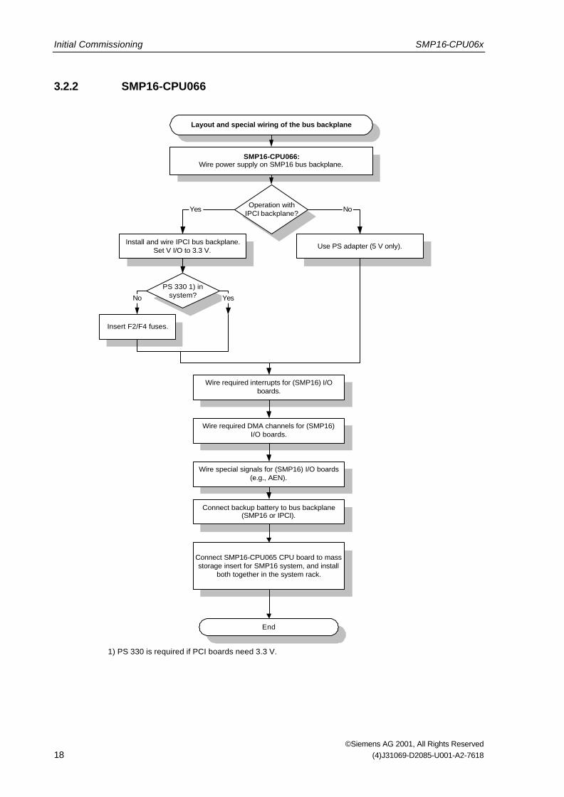
3.2.2 SMP16-CPU066
Wire required interrupts for (SMP16) I/Oboards.
Wire required DMA channels for (SMP16)I/O boards.
Wire special signals for (SMP16) I/O boards(e.g., AEN).
Connect backup battery to bus backplane(SMP16 or IPCI).
End
Layout and special wiring of the bus backplane
SMP16-CPU066:Wire power supply on SMP16 bus backplane.
Install and wire IPCI bus backplane.Set V I/O to 3.3 V.
Connect SMP16-CPU065 CPU board to massstorage insert for SMP16 system, and install
both together in the system rack.
Yes
Use PS adapter (5 V only).
NoOperation withIPCI backplane?
PS 330 1) insystem?No
Insert F2/F4 fuses.
Yes
1) PS 330 is required if PCI boards need 3.3 V.

SMP16-CPU06x Initial Commissioning
©Siemens AG 2001, All Rights Reserved(4)J31069-D2085-U001-A2-7618 19
3.3 Switching from SMP16-CPU055 to SMP16-CPU065
Keep the following points in mind when switching from an SMP16-CPU055 to an SMP16-CPU065 inan existing SMP16 system.
• The SMP16-CPU065can be installed directly in the slot of the SMP16-CPU055.
• The IPCI bus plug connector must at least be powered with the PS adapter (only 5 V required).
• When an IPCI backplane and IPCI cards are used, the backplane must be wired. Remember thatthe 3.3 volts from the SMP16-CPU065 are not available to the IPCI bus.
• The VIO (reference voltage for the signal level on the IPCI bus) must be set to 3.3 V. All IPCI I/Oboards must use the VIO of the backplane bus.
• When an IPCI backplane with HD/FD-UNI-I/O wiring is used, one slot should be left free on theleft side to leave room for the new design (new drive insert).
The table below shows the differences between the SMP16-CPU065 and theSMP16 CPU055
Function SMP16-CPU055 SMP16-CPU065
3.3 volt power supply Required from external source. Feedin over PS adapter or IPCIbackplane.
On board
SMP16 register can beread back.
No All registers can be read back in the area0178h to 017Fh.Starting with KS02:
Area 0138h to 013Ch
SMP16 bus interfacecan be switched off.
No Set R178 bit 7 = 1.(Also switch off SYSCLK/OSC)
Switch off clock pulseson the SMP16 bus(8.33 MHz and14.318 MHz)
No Set R178 bit 6 = 1.(Bit 7 = 0 required)
Starting with KS02:R13B bit 6, 7 - single enable
possible
Watchdog can be readback.
No R17E bit 7 = 1 after restart (no power on)indicates that a watchdog reset took place.Writing R17E bit 7 = 1 deletes the bit.
Watchdog time can beset.
Two times (approx. 100 msec, 1 sec) Adjustable between 96 msec and 960 msecR17E Bit 3,4,5
Additional counter block No Access via R134-R137
R17C Bit 3, 4 Input clock pulse counter,ZZ0 and ZZ1 can be set.
Bit 4 Cascading ofcounters ZZ0 and ZZ1possible
R17C Bit 2 Counter enableStarting with KS02:R13B Bits 0,1,2 Clock pulses can be
enabled separately.Bits 3, 4, 5 Gates can be addressed
separately.R13C Bits 0,1,2 Clock pulses can be
addressed with DI.Bits 4,5,6 Gates can be addressed
with DI.

Initial Commissioning SMP16-CPU06x
©Siemens AG 2001, All Rights Reserved20 (4)J31069-D2085-U001-A2-7618
Function SMP16-CPU055 SMP16-CPU065
Interrupt matrix foradditional interrupt block
No Electronic interrupt matrix
R178 Bit 0,1,2 Interrupt enable andselection
Additional interrupt block No Controller for various events (outputs ofadditional counters, DREQ signals of theSMP16 bus)
R130/131 Registers of the extra8259 (ICW, OCW)
R133 read INTA add. 8259
Cascaded interrupts onthe SMP16 bus
No Starting with KS02:Additional interrupt controller on SMP16 buscan be cascaded.R178 Bit 3 Enable CAS_EN
Buffered SRAM No Maximum of 128 kbytes
R17A Base addressR17D Bit 5, 6, 7 Enable and length
of the window.
Digital inputs/outputs,TTL level
No Starting with KS02:wo 8-bit ports can be parameterized as inputor output.R138/9 Data portsR13A Control regis terPort 0 can also be set as clock pulse and gateinputs of the additional counter.R13C Parameterization
Serial EEPROM Access via GPP2 of the FDC37C932
(0EAh/0EBh bits 0 to 2: DI, DO,CLK)
Access via GPP2 of the PIIX4E
R4035 Bit 2: Clock pulse for ser.EEPROM
(GPO10)R4035 Bit 1 Data for ser. EEPROM
(GPO9)R4032 Bit 1 Data from ser. EEPROM
(GPI17)
USER LED Two LEDs can be addressed viaGPIO of the FDC37C932, can beused (via jumper) for the hard diskchannels to indicate access.
Four LEDs can be used for on-boardindications (via BIOS Setup or SW).R17C Bit 0-3 Default USER
USER LED can be address via GPO ofPIIX4E.R4034 Bit 0 LED 0 (GPO0)R4035 Bit 1 LED 1 (GPO8)R4037 Bit 3 LED 2 (GPO27)R4037 Bit 4 LED 3 (GPO28)
SMP_INT Fixed on IRQ15 For PC compatibility's sake, IRQ15 ispermanently assigned to the secondary EIDEchannel.SMP_INT can only be fed in with one of theSMP_IRQs.Starting with KS02:
Depending on the EIDE channelSMP_INT is assigned toIRQ14 or IRQ15 (or neither of the two).

SMP16-CPU06x Initial Commissioning
©Siemens AG 2001, All Rights Reserved(4)J31069-D2085-U001-A2-7618 21
Note:• Since the Elite BIOS of the SMP16-CPU06x calculates the hard disk parameters differently than
the Power BIOS of the SMP16-CPU055 (in LBA mode), the hard disk may have to bereformatted and a new installation performed.
• When an SMP16-CPU055 is to be used instead of anSMP16-CPU06xa 3.3 V power supply is mandatory.
3.4 Scope of Delivery
The SMP16-CPU06x is delivered with or without AGP expansion based on your order. The modelwithout the AGP option requires two slots while the version with the AGP option needs three slots.
The IPCI-CPU066 or CPCI-CPU066 is the same as SMP16-CPU06x but without an SMP16 businterface board. This means the following functions are not available.
• Additional interrupt controller
• Additional counter block
• Buffered SRAM
The SMP16-CPU06x no longer includes a power supply adapter (PS adapter) for providing the 5 Volton the IPCI/CPCI bus connection. It must be ordered separately. The PS adapter is not required whenan IPCI(CPCI backplane is used.
Two fuses for the VIO supply of the backplane are included with the SMP16-CPU065 . These fusesmust be installed when no 3.3 V voltage supply is available in the system and thus there is also no 3.3V VIO reference voltage for the IPCI bus.
If this is the case, switches S1-3/4 must be closed on the SMP16-CPU066. The VIO jumper on theCPCI backplane must be set to 3.3 Volt.

Initial Commissioning SMP16-CPU06x
©Siemens AG 2001, All Rights Reserved22 (4)J31069-D2085-U001-A2-7618

SMP16-CPU06x Features
©Siemens AG 2001, All Rights Reserved(4)J31069-D2085-U001-A2-7618 23
4 FeaturesThe SMP16-CPU06x is an IBM-PC/AT-compatible CPU board for use on SICOMP-SMP16 industrialmicrocomputers. It has a metal front for individual locking. It requires two or three slots depending onthe model.
The board is of sandwich design consisting of the following (depending on the model).
• AGP model (as seen from the front)
- Left = AGP board
- Middle = CPU board
- Right = SMP16 bus interface
• Model without AGP (as seen from the front)
- Left = CPU board
- Right = SMP16 bus interface
Note:The SMP16-CPU06x can only be used on SMP16 bus backplanes. SMP bus backplanes are notsuitable since they are missing signal lines. Use without an SMP16 bus backplane is possible.
The or IPCI-CPU065 CPCI-CPU066 is the same as the SMP16-CPU06x but without the SMP16interface for use with IPCI/CPCI systems without SMP16 bus connection. It has a metal front forindividual locking. It requires two or three slots depending on the model.
• AGP model (as seen from the front)
- Left = AGP board
- Middle = CPU board
• Model without AGP (as seen from the front)
- Left = CPU board
Attention:The rest of this technical description only describes the SMP16-CPU06x. The IPCI-CPU065 or CPCI-CPU066 does not have any of the functions which are implemented on the SMP16 expansion board(SMP16 bus interface, SRAM, timer, additional interrupt controller, digital inputs/outputs, standarddrive interfaces).
Features SMP16-CPU06x
©Siemens AG 2001, All Rights Reserved24 (4)J31069-D2085-U001-A2-7618
Features of the SMP16-CPU06x
• Since the board is equipped with an IPCI bus connection in addition to the SMP16 bus, it can onlybe installed on the first SMP16 bus slot from the left.
• The board has an U-profile front plate with lever-pull handle and is prepared for EMC contactsprings.
• The CPU generates the 3.3 V itself. When additional IPCI/CPCI or SMP16 boards with 3.3 V areused, an extra 3.3 V supply is required.
CPU board
• Pentium-II/III Mobile Module inside
- Mobile Pentium II/III processor
- Chipset 82440BX from Intel, only North-Bridge (82443 BX)
- Second level cache (L2 cache)
- Power supply for processor core
• DRAM (SDRAM: only synchronous DRAM), max. of 256 Mbytes
• ISA–Bridge (South-Bridge) PIIX4E (82371 EB)
• AMD-LAN controller, 10/100 MBaud (79C 973)
• Clock pulse generation
• DC/DC converter for 3.3 V on board
• BIOS flash, up to 1 Mbyte
• Super I/O block integrated (FDC 37C 672)
- Keyboard controller
- Floppy disk controller
- Serial interfaces
- Parallel interface
• Reset/watchdog logic
• LEDs: RUN, WD, 2 x LAN, 4 x USER
• Bus interfaces
- IPCI/CPCI bus (065/066)
- UNI-I/O with HD/FD signals (secondary drive channel FD: drive B)
• Front plate interfaces
- Combined keyboard/mouse
- USB interface, single
- LAN (RJ45)
- COM A/COM B (RS 232)
- LPT (TTL)

SMP16-CPU06x Features
©Siemens AG 2001, All Rights Reserved(4)J31069-D2085-U001-A2-7618 25
SMP16 bus interface (can be ordered as option)
• Additional realtime functions (counter, interrupt controller)
• 128-kbyte buffered SRAM
• SMP16 bus interface
• Drive interfaces for SMP16 drive insert
- Hard disk interface (HD: primary channel)
- Floppy disk interface (FD: drive A)
AGP board (optional)
• Graphics controller from Silicon Motion LYNX E/EM
• 4-Mbyte video memory (SG-RAM)
• Max. resolution of 1024 x 768 pixels
• Analog VGA interface, alternate LVDS interface (can be changed with switch)
• PanelLink interface
• USB interface
• Voltage supply for PanelLink display

Features SMP16-CPU06x
©Siemens AG 2001, All Rights Reserved26 (4)J31069-D2085-U001-A2-7618
4.1 Microprocessor
The SMP16-CPU06x is equipped with the 32-bit Intel Pentium-II/III processor with a bus frequency of66/100 MHz. The PII/III Mobile Module with MMC2 connection is used.
4.2 Memory
4.2.1 BIOS
The board's BIOS is stored on a 1-Mbyte flash memory chip. The flash memory is permanentlyinstalled and can be reprogrammed on board (see chapter 10).
The BIOS is unpacked during startup (Post C3) and then copied to the DRAM (Post C5) which isshadowed in the memory area in place of the flash memory (shadow RAM function for the E/Fsegment). This speeds up the BIOS program functions.
The BIOS is compatible with the Elite BIOS V4.51 from the AWARD company. It contains a basicconfiguration of the board and its own Setup. For details, see chapter 9.3.
4.2.2 Working Storage
A Small Outline DIMM module is used for working storage. SDRAMs are used for optimumperformance. The memory module cannot be changed or expanded by the user.
4.2.3 Serial EEPROM
Configuration data are stored on the board's 256-byte EEPROM (type X24C02 (XICOR/ATMEL) withthe serial I2C bus interface. The contents of this chip are retained (even without battery backup) afterthe power supply is turned off. The first 64 bytes are reserved for manufacturer's data and may not beoverwritten.
Communication with this chip takes place via three bits in general-purpose port 2 (see chapter 7.2.3).These bits must be addressed as required by the I2C bus protocol. Two address bytes and one databyte must be transferred by bit for each byte to be sent.
4.2.4 SRAM Memory
The SMP16 board offers a 128-kbyte buffered SRAM.The maximum of 128 kbytes can be shadowed via register in various address areas or completelydeactivated (see chapter 9.1.10). A limited choice is available in BIOS Setup.

SMP16-CPU06x Features
©Siemens AG 2001, All Rights Reserved(4)J31069-D2085-U001-A2-7618 27
4.3 Chip Set
The AT functions of the SMP16-CPU06x are implemented with chip set 82440BX and supplementedwith Super I/O chip FDC 37C 672.
Chip Manufacturer Function
82443BX IntelSystem controller(DRAM control, PCI bus addressing, AGP bus interface)
82371EB IntelPCIISA-Bridge (PIIX4E)(Hard disk control, interrupt and DMA controller, counter,RTC, CMOS RAM, Power Management, USB, andGP I/O)
FD37C672 SMSC
Super I/O chip(Floppy disk controller, serial and parallel interfaces,keyboard interface and mouse interface)
4.3.1 Power Management
The chipset supports various Power Management functions which can be activated in BIOS Setup. Inparticular, APM V1.2 (Advanced Power Management) and ACPI (Advanced ConfigurationProgramming Interface - only S1 state) are implemented.
Power Management functions permit you to put the computer into various energy saver states afterspecified times (see BIOS description).
Operating systems such as Win9x and WinNT are built on these interfaces. These functions can nolonger be accessed under RMOS.
4.3.2 System Management Bus
The chipset (PIIX4E) contains a system-management-bus (SMB) host and slave interface. The PIIX4Ehost interface is used on the SMP16-CPU06x. The SDRAM module and the Pentium II Mobile Moduleare connected to the SMB.
On the PIIMM, both temperature sensors are connected to the SMB. These supply the currenttemperatures of the processor core and the BX chip.
The host interface is addressed in the I/O area starting at address 5000h (see programming notes inchapter 7).
4.3.3 Counters and Timers
The counter/timer unit of the PIIX4E chip has three 16-bit counters (Z0 to Z2) and is compatible withan 8254 chip. The counters have a fixed clock-pulse frequency of 1.193 MHz.
The counters are prewired for IBM-compatible operation.
• The gates of counters Z0 and Z1 fixed at +5 V.
• Counter Z0 generates the system time. Its output is permanently connected with IRQ0 inside thechip (see chapter 4.3.5).

Features SMP16-CPU06x
©Siemens AG 2001, All Rights Reserved28 (4)J31069-D2085-U001-A2-7618
• Counter Z1 initiates the refresh cycle of the DRAM controller. BIOS sets it to a clock pulseduration of 15.6 µsec.
• Counter Z2 is usually used to address a system loudspeaker (see chapter 4.3.8). It can beenabled or disabled with address 61h.
4.3.4 DMA Controller
The two 8237-compatible DMA controllers of the PIIX4E provide 8 DMA channels which are circuitedlike ATs.
Channel 8/16 Bits Function Remarks
CH0 8 1)
CH1 8 ECP printer 2)
CH2 8 Floppy disk -
CH3 8 1)
CH4 - Cascading -
CH5 16 1)
CH6 16 1)
CH7 16 -
1) The DMA channel is available on the SMP16 bus and can be requested by an external DMA source.2) Is programmed for LPT standard mode (Setup). 1) then applies.
Note:If the cascaded interrupts function of the additional interrupt controller is used in the application withthe SMP16-CPU065 starting at KS02, no other DMA channels are available on the SMP16 busexcept the DMA channel (DREQ3/DACK3*).
4.3.5 Interrupt Controller
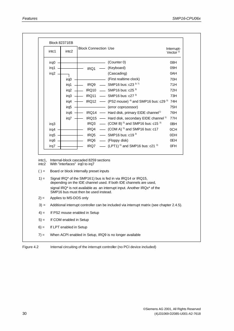
The interrupt controller function is compatible with two cascaded 8259 controllers. They are circuitedto be compatible with AT. A total of 14 interrupt inputs are available on PIIX4E. Figure 4.1 shows thecircuiting of internal controllers intc1 and intc2 as well as the interface and presettings of the board.
Interrupt INT can be cascaded further on the SMP16 bus. This requires a separate interrupt routinewhich is explained in the description of the INTA* generation register in chapter 7.2.1.10.
The unassigned connections of the interrupt controller are connected to the SMP16 bus where theycan be wired (see chapter 5.1).
BIOS automatically assigns the PCI interrupts to the available ISA interrupts (maximum of four). Theseinterrupts are then no longer available on the SMP16 bus.
Note:Various interrupts for automatic routing by BIOS can be disabled in Setup (see Setup in chapter9.1.7).

SMP16-CPU06x Features
©Siemens AG 2001, All Rights Reserved(4)J31069-D2085-U001-A2-7618 29
Attention:If too many interrupts are disabled (setting Legacy ISA) in BIOS Setup (PnP Configuration) for theautomatic routing for PCI components which require an interrupt, additional interrupts may not beable to be assigned to all devices/any devices. These PCI bus components can no longer be used.
Configuration on the SMP16-CPU06x (BIOS defaults)
SMP16-CPU065 SMP16-CPU066
Secondary EIDE channel: IRQ15 2) disabled 3)
Primary EIDE channel: IRQ14 2) IRQ14 2)
PS/2 mouse: IRQ12 1) IRQ12 1)
USB interface: IRQ11 1) IRQ15 1)
LAN interface: IRQ11 1) IRQ15 1)
On-board LPT: IRQ7 1) IRQ7 1)
Floppy disk controller: IRQ 6 disabled 3)
AGP controller: - -On-board COM A: IRQ4 1) IRQ4 1)
On-board COM B: IRQ3 1) IRQ3 1)
1) Free for the SMP16 bus if disabled in BIOS Setup (see there)2) Available for the SMP-INT depending on the enabled IDE channel
3) Channel deactivated to prevent hardware damage if wrong 64-bit CPCI backplane is used
Attention:Starting with BIOS versions 1.03 or 2.03 (for upper levels KS01 or KS1x/KS02 of the SMP16-CPU065), the IRQ for LAN and USB can be deactivated in BIOS Setup. Automatic routing for the PCIbus starts at IRQ15 (if free).IRQ14 and IRQ9 are excluded from the automatic interrupt routing for the PCI bus.
The PCI bus has four INT lines (INTA to INTD). BIOS routes these to up to four PC IRQs. With amaximum of four slots on the IPCI bus and the PCI devices on board, this means that several devicesmust share an interrupt. PCI device drivers support this, and BIOS switches these IRQs from edge-triggered to level-triggered (see chapter 7.2).
Attention:Currently, RMOS does not support level-triggered interrupts.
Features SMP16-CPU06x
©Siemens AG 2001, All Rights Reserved30 (4)J31069-D2085-U001-A2-7618
intc1 intc2
irq0irq1
irq2
irq0irq1
irq2
irq3
irq4
irq5
irq6
irq7
irq3
irq4
irq5irq6
irq7
Block Connection
IRQ1
IRQ9
IRQ10
IRQ11
IRQ12
IRQ14
IRQ15IRQ3
IRQ4
IRQ5IRQ6
IRQ7
Use
(Counter 0)
(Keyboard)
(Cascading)
(First realtime clock)
SMP16 bus: c23 3) 7)
SMP16 bus: c25 3)
SMP16 bus: c27 3)
(PS2 mouse) 4) and SMP16 bus: c29 3)
(error coprozessor)
Hard disk, secondary EIDE channel 1)
(COM B) 5) and SMP16 bus: c15 3)
(COM A) 5) and SMP16 bus: c17
SMP16 bus: c19 3)
Hard disk, primary EIDE channel1)
(Floppy disk)
(LPT1) 6) and SMP16 bus: c21 3)
Interrupt- Vector 2)
08H09H
0AH
70H
77H
0BH
0CH
0DH0EH
0FH
71H
72H
73H
74H
75H
76H
Block 82371EB
intc1, intc2
Internal-block cascaded 8259 sectionsWith "interfaces" irq0 to irq7
( ) = Board or block internally preset inputs
1) = Signal IRQ* of the SMP161) bus is fed in via IRQ14 or IRQ15, depending on the IDE channel used. If both IDE channels are used,signal IRQ* is not available as an interrupt input. Another IRQx* of the SMP16 bus must then be used instead.
2) = Applies to MS-DOS only
3) = Additional interrupt controller can be included via interrupt matrix (see chapter 2.4.5).
4) = If PS2 mouse enabled in Setup
5) = If COM enabled in Setup
6) = If LPT enabled in Setup
7) = When ACPI enabled in Setup, IRQ9 is no longer available
Figure 4.2 Internal circuiting of the interrupt controller (no PCI device included)

SMP16-CPU06x Features
©Siemens AG 2001, All Rights Reserved(4)J31069-D2085-U001-A2-7618 31
SMP16 interrupts
Note:The LAN controller can be disabled in BIOS (see chapter 8.1.9).
Interrupts IRQ3, IRQ4, IRQ7 and IRQ12 are used by internal components (COM B, COM A or LPT1,PS2 mouse).
COM A or COM B • On board, active ("enable" in BIOS Setup)IRQ4/IRQ3 are assigned.
SMP16-IRQ can't get through.
LPT1• On board, active ("enable" in BIOS Setup)
IRQ7/IRQassigned.SMP16-IRQ can't get through.
PS2 mouse• On board, active ("enable" in BIOS Setup)
IRQ12/IRQ assigned.SMP16-IRQ can't get through.
Attention:When "ACPI Function" is enabled in Setup (see chapter 9.1.6), IRQ9 is used by the ACPI functionand is no longer available on the SMP16 bus.
Note:If the extra interrupt controller is used (see chapter 4.7.2), its interrupt output can be routed to one ofthe SMP interrupts (see chapter 7.2.1.7). This interrupt output is then no longer available on theSMP16 bus.Use of the extra interrupt controller provides five additional interrupts (DREQx* signals of the SMP16bus). The additional interrupts are handled as described in chapter 7.2.1.1.
4.3.6 NMI Generation
The NMI logic is controlled in 2 registers (see chapter 7.2.1).
• Register 61hNMI status information
Bit 7: SERR# of the PCI busBit 6: IOCHCK# of the ISA bus
NMI enableBit 3: IOCHCK# 0 = enable, 1 = disableBit 2: SERR# 0 = enable, 1 = disable
• Register 70hBit 7: General NMI enable
0 = enabled1 = disabled

Features SMP16-CPU06x
©Siemens AG 2001, All Rights Reserved32 (4)J31069-D2085-U001-A2-7618
4.3.7 Bus Timing
BIOS sets the board to the optimum speed for memory and bus accesses. The ISA bus which is clock-pulsed with 8.33 MHz is the basis of SMP16 bus timing.
Timing of the PC-AT-compatible CPU boards is based on the ISA specification IEEE-P996 (draft).
With 16-bit accesses, the I/O must return the RDYIN signal within a maximum of 82 nsec (77 nsec onthe SMP16 bus due to additional decoding and bus driver) after the activated command so that waitcycle are inserted.The SMP16 specifications state the time as a maximum of 100 nsec. A "Not Ready" can be set toensure this maximum time (see chapter 7.2.1.6). Boards with the ASBIC to the SMP16 bus interfacedo not have critical time problems.
You can also set the bus timing for 16-bit accesses in accordance with SMP16 specifications (seechapter 7.2.1.9). Activation of a "Not Ready" is mandatory here, and the command takes a minimum of500 nsec in accordance with SMP16 specifications.
Note:An external "Ready" (RDYIN signal) can extend the bus cycle even further.
The I/O can use the OWS* signal of the SMP16 bus to shorten the cycle.
The I/O recovery time (time between two consecutive I/O accesses) can be increased in BIOS Setupto correct any timing problems with I/O boards.
There are no recovery settings in the memory area. The access sequence can only be influenced byinserting dummy read/write cycles, for instance.
4.3.8 Addressing the Loudspeaker
The output of counter Z2 is circuited as special signal SPEAKER to connection b10 of the SMP16 businterface (for addressing, see chapter 7.2.1). A system loudspeaker can be connected directly there to+5 V or to an amplifier (see also the signal specifications in chapter 5.1.4).

SMP16-CPU06x Features
©Siemens AG 2001, All Rights Reserved(4)J31069-D2085-U001-A2-7618 33
4.4 Drive Controller
Floppy disk drives
Two floppy disk drives (5.25" and/or 3.5") can be connected to the floppy disk drive controller. Thefloppy disk drive controller uses IBM-PC/AT interrupt 6 (IRQ6) and DMA channel 2 (DRQ2, DACK2*).
The floppy disk drive controller supports the following floppy disk formats.
Type Formatted
5.25" 360 kbytes
5.25" 1.2 Mbytes
3.5" 720 kbytes
3.5" 1.44 Mbytes
3.5" 2.88 Mbytes
The interface of the floppy disk drives is 34-pin pin strip X8 on the configuration side of the SMP16board (LW A:), or the UNI I/O interface of the IPCI backplane or the rear panel I/O interface of theCPCI backplane (LW B:) when "uncrossed" cables are used.
Swap-Floppy in BIOS Setup (see chapter 8.1.4) can be used to set which of the two drives is to beaddressed as LW A. or LW.B.
Note:With KS01 of the SMP16-CPU065 , both interfaces are designed as LW A drives. Two floppy diskdrives can only be used when lines 10 - 16 are crossed in one of the two connection cables.Only one floppy disk drive may be connected via "uncrossed" connection cables.
With the SMP16-CPU066, the floppy disk drive controller must first be activated in BIOS Setup (seechapter 9.1.9).
Hard disk controller
The hard disk controller supports devices with enhanced integrated drive electronics (EIDE). Thisinterface is also frequently referred to as the AT interface. It supports all PIO modes, bus master DMAand UDMA/33.
The highly-integrated SB82371EB chip (see chapter 4.3) contains two of these interfaces. This meansthat up to 2 hard disks per channel can be connected to the SMP16-CPU06x.
Controller Hard Disks Pin Strip Interrupt
X6 (40-pin) IRQ 14Primary EIDE channel 1 1 and 2
X7 (44-pin, 2 mm apart) IRQ 14
Secondary EIDEchannel 2
3 and 4 UNI/rear panel I/O decoupling IRQ 15

Features SMP16-CPU06x
©Siemens AG 2001, All Rights Reserved34 (4)J31069-D2085-U001-A2-7618
Note:With the SMP16-CPU066, the secondary drive channel must first be activated in BIOS Setup (seechapter 9.1.9).
4.5 LAN Controller
The new 100-MBaud, LAN controller AM79C973 from AMD is used on the SMP16-CPU06x.
Technical Data
• One-chip PCI2WIRE Fast Ethernet controller, 10/100-MBaud physical layer integrated
• Dual-speed Carrier Sense Multiple Access/Collision Detect (CSMA/CD) (10 Mbytes and100 Mbytes) Media Access Controller (MAC) in acc. W. IEEE 802.3 and Blue Book EthernetStandards
• Meets PC99 and NET PC specifications
• Wake on LAN prepared
• Boot RAM integrated in system BIOS, can be activated in Setup (see chapter 9.1.4).
• Automatic recognition of 10/100 MBaud
The network interface is an RJ45 plug-in connection (10BaseT, 100BaseT2).
Note:The LAN controller can be disabled in BIOS Setup (see chapter 9.1.9).
4.6 VGA Graphics Expansion
Graphics controller
Graphic controllers from Silicon Motion are used.
The controllers have separate connections for CRT and display. They can represent two separatescreens over these interfaces with a maximum resolution of 1280 x 1024 pixels.
Up until construction state KS02 of the AGP module, the SM811 with 2 Mbytes of integrated memoryis used. The SM811 can handle an additional 2 Mbytes of external SGRAM.
Starting with construction state KS03 of the AGP module, the SM710 with 4 Mbytes of integratedmemory is used. External memory is then no longer necessary.
Graphics memory
Up until KS02, an additional 2 Mbytes of SGRAM are provided on the board. Total memory is thenalways 4 Mbytes.

SMP16-CPU06x Features
©Siemens AG 2001, All Rights Reserved(4)J31069-D2085-U001-A2-7618 35
Video BIOS
The BIOS from the Silicon Motion company is used without any modifications to the standard settings.
This means that, up to construction status KS02, dual-screen support is always implemented (analog:CRT, digital: LVDS/PanelLink, Single Pixel Mode).
Attention:Up to KS02, the resolution is set at the factory to 640 x 480 pixels due to the dual-screen support(see setting of the display resolution). During startup, a screen repetition frequency of exactly 60 Hzis set for fixed-frequency monitors.When the graphics driver is loaded later and a resolution of more than 640 x 480 pixels is set, thevisible area on the monitor screen remains limited to 640 x 480 pixels.To keep this from happening, the higher resolution must be set beforehand. The display duringstartup is smaller (640 x 480 pixels) - visible in the middle of the 1024 x 768 pixels.
Starting with KS03 of the AGP module, display support can be activated with switch S2 (see below).Only VGA analog (CRT) is set at the factory. In this setting, the switches for the display resolutionhave no meaning.
Display connection
The AGP board is equipped with two display interfaces.
• LVDS interface
• PanelLink interface
Both connections support an up to 24-bit depth of tone at one pixel per clock pulse.
Activating display support (starting with KS03 of the AGP module)
Switch S2Function
6
Only analog VGA interface active (setting at the factory) OFF
Display interfaces also active ON
Note:The following settings can be ignored if only CRT mode is being used.
Switch S2 ON means: Switch is pointing toward the PCB of the AGP graphics card.
The LVDS connection is made on the 15-pin sub D socket, parallel to the CRT connection. Thismeans that LVDS and CRT cannot be used simultaneously. DIP switch S1 on the AGP module isused to switch between CRT and LVDS (cf. figure 4.4).
Note:The AGP module must be demounted before CRT can be switched to LVDS. The module may onlybe demounted by qualified personnel.

Features SMP16-CPU06x
©Siemens AG 2001, All Rights Reserved36 (4)J31069-D2085-U001-A2-7618
The PanelLink interface is a 26-pin, mini-delta ribbon socket (MDR26). It is completely separate fromthe CRT interface.
Settings for display support
• Connecting the display controller (S3)Setting the interface
Switch S3Function
2 1
PanelLink + LVDS OFF OFF
LVDS OFF ON
PanelLink + CRT (factory setting) ON OFF
CRT ON ON
• Switching between LVDS and CRT (S1)8-fold DIP switch for the CRT/LVDS interface
Switch S1
8 7 6 5 4 3 2 1
Analog VGA for monitor (factory setting) ON ON ON ON ON ON ON OFF
LVDS data for display OFF OFF OFF OFF OFF OFF OFF ON
Not permitted All other combinations
Warning
When setting the switches, remember that switches S1 and S3 (cf. figure 4.4)must be coordinated (i.e., either LVDS or CRT must be set for both switches). Acombination of both will cause malfunctions. PanelLink can be switched regardlessof S1.
• Settings for startup (S2)Clock pulse selection for display
Switch S2Function
1
Normal ON
Inverted (factory setting) OFF
Note:Switch S2 ON means: Switch is pointing toward the PCB of the AGP graphics card.
SMP16-CPU06x Features
©Siemens AG 2001, All Rights Reserved(4)J31069-D2085-U001-A2-7618 37
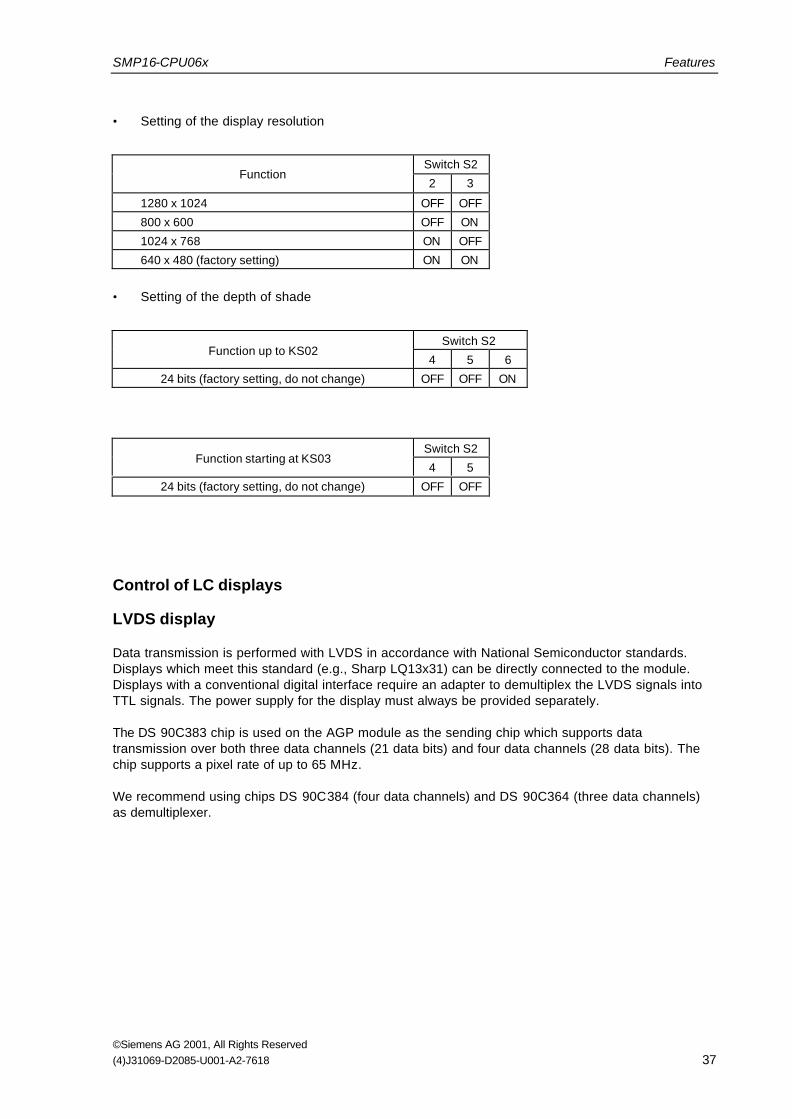
• Setting of the display resolution
Switch S2Function
2 3
1280 x 1024 OFF OFF
800 x 600 OFF ON
1024 x 768 ON OFF
640 x 480 (factory setting) ON ON
• Setting of the depth of shade
Switch S2Function up to KS02
4 5 6
24 bits (factory setting, do not change) OFF OFF ON
Switch S2Function starting at KS03
4 5
24 bits (factory setting, do not change) OFF OFF
Control of LC displays
LVDS display
Data transmission is performed with LVDS in accordance with National Semiconductor standards.Displays which meet this standard (e.g., Sharp LQ13x31) can be directly connected to the module.Displays with a conventional digital interface require an adapter to demultiplex the LVDS signals intoTTL signals. The power supply for the display must always be provided separately.
The DS 90C383 chip is used on the AGP module as the sending chip which supports datatransmission over both three data channels (21 data bits) and four data channels (28 data bits). Thechip supports a pixel rate of up to 65 MHz.
We recommend using chips DS 90C384 (four data channels) and DS 90C364 (three data channels)as demultiplexer.

Features SMP16-CPU06x
©Siemens AG 2001, All Rights Reserved38 (4)J31069-D2085-U001-A2-7618
Table 4.1 Allocation of the LVDS data signals
Controller LVDS Channel 90C383 (Tx Name) Color Bit (24-Bit)
FPDATA0 3 IN17 B0
FPDATA1 3 IN16 B1
FPDATA2 1 IN15 B2
FPDATA3 1 IN18 B3
FPDATA4 2 IN19 B4
FPDATA5 2 IN20 B5
FPDATA6 2 IN21 B6
FPDATA7 2 IN22 B7
FPDATA8 3 IN11 G0
FPDATA9 3 IN10 G1
FPDATA10 0 IN7 G2
FPDATA11 1 IN8 G3
FPDATA12 1 IN9 G4
FPDATA13 1 IN12 G5
FPDATA14 1 IN13 G6
FPDATA15 1 IN14 G7
FPDATA16 3 IN5 R0
FPDATA17 3 IN27 R1
FPDATA18 0 IN0 R2
FPDATA19 0 IN1 R3
FPDATA20 0 IN2 R4
FPDATA21 0 IN3 R5
FPDATA22 0 IN4 R6
FPDATA23 0 IN6 R7
LP/HSYNC 2 IN24 HSYNC
FP/VSYNC 2 IN25 VSYNC
M/DE 2 IN26 ENABL
VBIASEN 3 IN23 ENAVEE_
The ENAVDD signal is available directly on the sub D socket to control the supply voltage. The DDCsignals can be used to set a contrast voltage, for instance. The switching signal for a negative contrastvoltage (ENAVEE_) is only available when four-data-channel transmission is used.
PanelLink display
Data transmission is performed in accordance with the PanelLink technology of Silicon Image. Thistransmission procedure is used by the Digital Display Working Group (DDWG) for the Digital VisualInterface (DVI) (DVI revision 1.0 dated 04.02.1999). Displays which meet this standard (e.g., TFTdisplay LM151X1 from LG Philips) can be directly connected to the module. Displays with aconventional digital interface require an adapter to demultiplex the PanelLink signals into TTL signals.The plug connector offers the power for the display.
The SIL140 chip from Silicon Image is used on the AGP module as the sending chip. The chipsupports a pixel rate of up to 85 MHz.
SMP16-CPU06x Features
©Siemens AG 2001, All Rights Reserved(4)J31069-D2085-U001-A2-7618 39
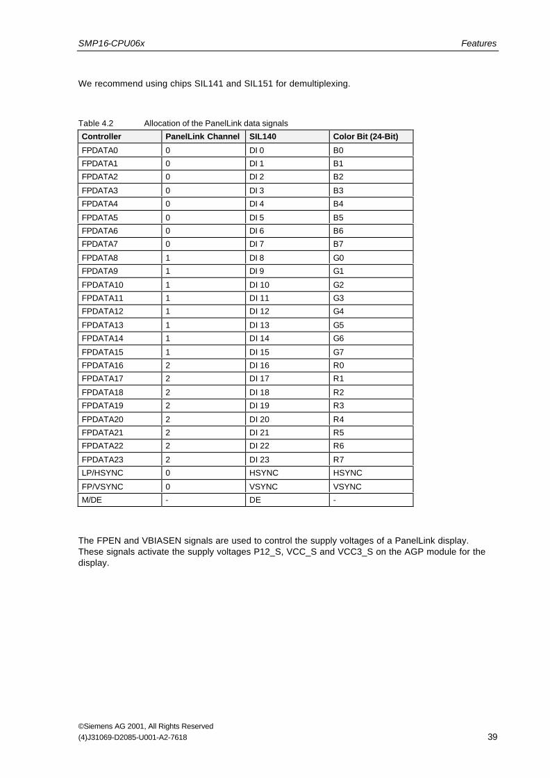
We recommend using chips SIL141 and SIL151 for demultiplexing.
Table 4.2 Allocation of the PanelLink data signals
Controller PanelLink Channel SIL140 Color Bit (24-Bit)
FPDATA0 0 DI 0 B0
FPDATA1 0 DI 1 B1
FPDATA2 0 DI 2 B2
FPDATA3 0 DI 3 B3
FPDATA4 0 DI 4 B4
FPDATA5 0 DI 5 B5
FPDATA6 0 DI 6 B6
FPDATA7 0 DI 7 B7
FPDATA8 1 DI 8 G0
FPDATA9 1 DI 9 G1
FPDATA10 1 DI 10 G2
FPDATA11 1 DI 11 G3
FPDATA12 1 DI 12 G4
FPDATA13 1 DI 13 G5
FPDATA14 1 DI 14 G6
FPDATA15 1 DI 15 G7
FPDATA16 2 DI 16 R0
FPDATA17 2 DI 17 R1
FPDATA18 2 DI 18 R2
FPDATA19 2 DI 19 R3
FPDATA20 2 DI 20 R4
FPDATA21 2 DI 21 R5
FPDATA22 2 DI 22 R6
FPDATA23 2 DI 23 R7
LP/HSYNC 0 HSYNC HSYNC
FP/VSYNC 0 VSYNC VSYNC
M/DE - DE -
The FPEN and VBIASEN signals are used to control the supply voltages of a PanelLink display.These signals activate the supply voltages P12_S, VCC_S and VCC3_S on the AGP module for thedisplay.

Features SMP16-CPU06x
©Siemens AG 2001, All Rights Reserved40 (4)J31069-D2085-U001-A2-7618
Address areas of the graphics controller
The graphics hardware is fully (i.e., hardware and software) compatible with the VGA standard (VideoGraphics Array). Analog VGA monitors (standard PS/2 compatible) or multisync monitors can beconnected.
The monitor screen memory of the graphics adapter is 4 Mbytes in size and is addressed in theaddress area from A0000h to BFFFFh and linearly via the PCI bus.
The graphics controller handles addressing in a 64-kbyte window and mapping. The included driversaddress the 4-Mbyte monitor screen memory linearly in the PCI memory area.
The VGA BIOS is located on a flash EPROM (128k x 8). BIOS is located in the address area fromC0000h to CBFFFh (48 kbytes).
The graphics controller uses the I/O address areas listed below.
I/O address area
Table 4.3 I/O address areas for the graphics controller
Port Address Read Register Write Register
3B4h CRTC Index Register CRTC Index Register
3B5h CRTC Data Register CRTC Data Register
3BAh Input Status Register Feature Control Register
3C0h Attribute Controller Index / Data Register Attribute Controller Index / Data Register
3C1h Attribute Controller Index / Data Register Attribute Controller Index / Data Register
3C2h Input Status Register 0 Miscellaneous Output Register (MSR)
3C4h Sequencer Index Register Sequencer Index Register
3C5h Sequencer Data Register Sequencer Data Register
3C6h DAC Mask Register DAC Mask Register
3C7h DAC Status Register DAC Address Read Register
3C8h DAC Address Write Register DAC Address Write Register
3C9h DAC Data Register DAC Data Register
3CEh Graphics Controller Index Register Graphics Controller Index Register
3CFh Graphics Controller Data Register Graphics Controller Data Register
03D4h CRTC Index Register CRTC Index Register
03D5h CRTC Data Register CRTC Data Register
03DAh Input Status Register Feature Control Register

SMP16-CPU06x Features
©Siemens AG 2001, All Rights Reserved(4)J31069-D2085-U001-A2-7618 41
Memory address areas
007F FFFFH
0040 8000H
0040 7FFFH
Drawing prozessor data (32 kbytes)
0040 0000H
Monitor screen memory 4 Mbytes
0000 0000H
003F FFFFH
0040 C000H
0050 0000H
PCI base address of the AGP module
0040 BFFFH
0040 E000H0040 DFFFH
0041 0000H0040 FFFFH
Drawing processor register (16 kbytes)
Video processor register (8 kbytes)
Capture processor register (8 kbytes)
004F FFFFH
PCI memory area
0070 0000H006F FFFFH
Additional data portDrawing processor
Memory mapped I/O register
Figure 4.3 Memory address areas of the AGP graphics controller
4.7 Realtime Functions
4.7.1 Additional Counter/Timer Block
The SMP16 board has an extra counter block (82C54) for realtime applications. The three counters ofthis block can be pulsed as shown below.
• Counter ZZ0 with either 8.33 MHz or 14.318 MHz
• Counter ZZ1 with either 14.318 MHz or the output of ZZ0
Features SMP16-CPU06x
©Siemens AG 2001, All Rights Reserved42 (4)J31069-D2085-U001-A2-7618
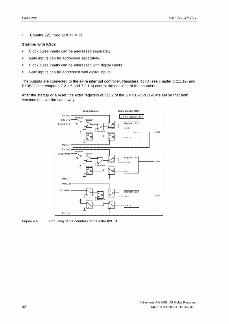
• Counter ZZ2 fixed at 8.33 MHz
Starting with KS02
§ Clock pulse inputs can be addressed separately.
§ Gate inputs can be addressed separately.
§ Clock pulse inputs can be addressed with digital inputs.
§ Gate inputs can be addressed with digital inputs.
The outputs are connected to the extra interrupt controller. Registers R17D (see chapter 7.2.1.12) andR13B/C (see chapters 7.2.1.5 and 7.2.1.6) control the enabling of the counters.
After the startup or a reset, the extra registers of KS02 of the SMP16-CPU06x are set so that bothversions behave the same way.
Extra counter (8254)
Register 134 h
Control register 137 h8.33 MHz
14.318 MHz
Port1(0)R17D Bit3=0
R17D Bit2=0
R13B Bit0=1
Port1(3)
CLK_ZZ0
GATE_ZZ0
Register 135 h
14.318 MHz
Port1(2)R17D Bit4=0
R17D Bit2=0
R13B Bit1=1
Port1(4)
CLK_ZZ1
GATE_ZZ1
OUT_ZZ0 ZINT0
ZINT1
R13B Bit3=1 R13C Bit3=1
R13C Bit0=1
R13C Bit1=1
R13C Bit4=1R13B Bit4=1
Register 136 h8.33 MHz
Port1(2)
R17D Bit2=0
R13B Bit2=1
Port1(5)
CLK_ZZ1
GATE_ZZ1
ZINT2R13C Bit2=1
R13C Bit5=1R13B Bit5=1
Control register
Figure 4.4 Circuiting of the counters of the extra 82C54

SMP16-CPU06x Features
©Siemens AG 2001, All Rights Reserved(4)J31069-D2085-U001-A2-7618 43
4.7.2 Additional Interrupt Controller
The SMP16-CPU06x has an extra 82C59 interrupt controller for realtime applications in addition to thePC-compatible interrupt system.
INT
A*
IRQ
*1
NM
I*
IRQ
<3,4
,5,7
,9,1
0,11
,12>
*C
orre
spon
ds to
IRQ
<3/
4/5/
7/9/
10/1
1/12
>
SM
P16
-Bus
1
82C
59
INT
INTA
IR7
IR6
IR5
IR4
IR3
IR2
IR1
IR0
TM
R_O
UT
2T
MR
_OU
T1
TM
R_O
UT
0
88
Z_I
NT
.
Reg
iste
r 13
3I/O
-Rea
d 13
3h
Reg
iste
r S
MP
_IN
TA
I/O-R
ead
17B
h
8259
INT
INT
AIR
7IR
6IR
5IR
4IR
3IR
2IR
1IR
0
IRQ
15IR
Q14
IRQ
11IR
Q10
IRQ
9
8259
INT
INT
AIR
7IR
6IR
5IR
4IR
3IR
2IR
1IR
0
IRQ
4IR
Q3
IRQ
6IR
Q5
IRQ
7
Por
t_B
Reg
iste
r 61
h R
egis
ter 7
0h
INT
INT
A
IOC
HC
K
NM
I
Pen
tium
II
proc
esso
r
Inte
rrup
t m
atrix
for
extr
a in
terr
upt
(R17
8h)
PC
cor
e an
d ch
ipse
t
1
82C
54
DR
EQ
< 0
,1,3
,5,6
>*
01356
Ext
ra ti
mer
Ext
raIR
Q c
ontro
ller
IRQ
12
55
DA
CK
< 0,
5,6
>*/ C
AS
<0,1
,2>
3
DA
CK
< 1
>*/ Z
INT
A*
DA
CK
<0,1
,5,6
>
CA
S<0
,1,2
>
SP
/EN
*C
asca
ding
on S
MP
16 b
us
Z_I
NT
A.
Figure 4.5 nterrupt system of theSMP16-CPU06x
Features SMP16-CPU06x
©Siemens AG 2001, All Rights Reserved44 (4)J31069-D2085-U001-A2-7618
Interrupt Additional 82C59Input Source Vector
irq0 Output of extra counter ZZ0 80 h
irq1 Output of extra counter ZZ1 81 h
irq2 Output of extra counter ZZ2 82 h
irq3 DREQ0* 83 h
irq4 DREQ1* 84 h
irq5 DREQ3* 85 h
irq6 DREQ5* 86 h
irq7 DREQ6* 87 h
The output of the additional interrupt controller can be routed via interrupt matrix (register 178h,chapter 7.2.1.7) to the SMP16 interrupts (see figure 2.3).
The additional interrupt controller can be cascaded on the SMP16 bus. The least used signals areused (DACK0/5/6* as CAS0/1/2 and DACK1* as ZINTA). This operating mode is activated in bit 3 ofregister 178h (see chapters 7.2.1.7 and 7.2.1.1).
4.7.3 Digital Inputs/Outputs
Starting with KS02, the SMP16 expansion board is equipped with two 8-bit ports. These ports aredesigned as digital inputs/outputs and are applied to one plug-in connector each.
The two ports can be made available on the front plate with a ZUB (still to be defined). This requiresan additional slot.
Attention:The two ports only supply a 5 V level, and only a 5 V level can be applied to them (TTL level).
The two 8-bit ports (I/O address: 138/9h) can be parameterized as DI or DQ (I/O address: 13Ah).Basic setting after a reset: both ports as DI (see chapter 7.2.1.2).
Another choice is to use three signals each of port 0 as clock-pulse and gate inputs for the extracounter block (see chapter 7.2.1.6).

SMP16-CPU06x Features
©Siemens AG 2001, All Rights Reserved(4)J31069-D2085-U001-A2-7618 45
4.8 Safety Functions
4.8.1 Voltage Monitoring
The voltages VCC (+5 V) and VCC3 (+3.3 V) of the board are continuously monitored. When one ofthese voltages drops below its minimum value, a reset is triggered for the processor.
• Switching threshold for VCC: 4.72 V (±40 mV)
• Switching threshold for VCC3: 3.1 V
The power failure signal of a powerpack is usually connected to the NMI* input of the board so that,when a power failure occurs, the computer is able to perform an emergency routine during the follow-up time guaranteed by powerpacks.
4.8.2 Battery Buffering
When the network voltage drops below the battery voltage, the realtime clock, the CMOS RAM andthe SRAM are switched to battery powering. This ensures that the configuration data are retained.
The battery voltage (3.0 V to 4.5 V) can be applied over the SMP16 bus backplane or IPCI backplane.
A gold capacitor buffers the CMOS-RAM, SRAM and the clock when brief interruptions occur (theminimum data retention time for the clock and CMOS-RAM is 60 minutes).
4.8.3 Watchdog
Program execution monitoring can be enabled with watchdog enable register R17Eh. The watchdogtime can be programmed between 96 and 960 msec (see chapter 7.2.1.13).
The watchdog is not enabled at system start. If enabled, the watchdog triggers a CPU and systemreset if the user software does not issue a trigger-watchdog command (dummy read (R17Fh) for thewatchdog register) within a set time. If this happens, the red LED on the board's front plate goes on,and the HWWD* (b9) signal of the SMP16 bus interface is activated. After a new start, this state canbe detected by the software (R17Eh, bit 7 = 1).
Both indicators can be canceled by turning off the power supply or by writing bit 7 = 1 to I/O address17Eh. See also chapters 7.2.1.13 and 7.2.1.14.

Features SMP16-CPU06x
©Siemens AG 2001, All Rights Reserved46 (4)J31069-D2085-U001-A2-7618
4.8.4 Temperature Monitoring
The Pentium II Mobile Module is equipped with two temperature sensors which can be read by thesystem management bus (SMB). These sensors trigger an alarm when the temperature exceedscertain adjustable limits.
Starting with KS02 of the CPU065 board and the CPU066 board, the red error LED is activated foroptical indication. The temperature can be read on GPI 16 (4033h bit 0 = 0). See chapter 7.2.3.
Note:The temperature alarm of the Pentium II Mobile Module must be actively reset (see chapter 7.2.4).
BIOS sets the limits for CORE and BX temperature to 100° C. When this limit is reached, BIOSactivates so-called "throttling." The throttling rate is set to 75% (i.e., the CPU is only on 25% of thetime). Even at an ambient temperature of 55° C (e.g., failure of the fan), this ensures operation withinmodule specifications.
Note:The limit values are not reached when a fan is used (air throughput: 3 x 100 m3/h) and the ambienttemperature is 55° C.
4.8.5 Password Protection
BIOS can protect starting the boot program and changing the system configuration (CMOS-RAM) witha password. For details, see chapter 9.1.11.
4.8.6 LEDs
The front plate of the SMP16-CPU06x is equipped with eight LEDs.
LPT
WDRUN R
L1 L2 L3 L4
L
USB
Figure 4.6 Front plate with LEDs
RUN (green) Indicates that the board is accessing the PCI bus and outputting the FRAMEPCI signal (accesses to PCI, on-board and SMP16 I/O).

SMP16-CPU06x Features
©Siemens AG 2001, All Rights Reserved(4)J31069-D2085-U001-A2-7618 47
WD (red) If the watchdog is enabled, indicates that a reset has been triggered becausethe time was exceeded. Also indicates every temperature alarm triggeredwhen a certain temperature is exceeded.The user can use this LED when the watchdog is not on.
R (green) Shows activity on the LAN interface (receive)
L (green) LAN interface connected (link)
L 1 to L 4 (yellow) Available for status indicators from the user program or in Setup.
LED L1 and LED L2 can also be used separately as access indicators for thehard disks (L1 = primary channel, L2 = secondary channel). See Register tab.
LED L3 and LED L4 can be used instead for LAN to indicate collision (L3) andtransmit (L4) on the LAN interface.

Features SMP16-CPU06x
©Siemens AG 2001, All Rights Reserved48 (4)J31069-D2085-U001-A2-7618
4.9 Operation without Fan
4.9.1 Setting via Setup
Fanless operation can be set for the SMP16-CPU06x in BIOS Setup (see chapter 9.1.10). When thissetting is used, a throttling rate of 50% is set for the processor.This means that the power for the internal processor clock pulse is turned off within a time interval of244 sec, 122 sec.
A lower clock pulse frequency also means that board performance is lower. The CPU's powerconsumption drops to prevent temperature monitoring from being triggered even at an ambienttemperature of 55° C.
Attention:This throttling suppresses acceptance of interrupts for up to 122 sec. This must be considered andallowed for, particularly with realtime systems.
Attention:Operating systems that support power management (e.g., APM with Win9x) reset manual throttlingduring startup.
This also means that the no-fan setting is canceled in Setup.
4.9.2 Regulated Operation
The setting in Setup represents a fixed and necessary limitation and even an impossibility for somesystems.
Implementation of a monitoring task is simple when the SMB is used to determine the temperature(see chapter 6.2.4).
The task (e.g., watchdog task) uses an SMB to read the current temperature of the processor coreand/or the BX chip. When the temperature reaches a predefined limit, 12.5% is first set via manualthrottling (chapter 7.2.2). If this is not sufficient, the value can be increased in increments of 12.5%.This is repeated until a stationary value is reached. It may be possible to cancel throttling from time totime (include hysteresis).

SMP16-CPU06x Features
©Siemens AG 2001, All Rights Reserved(4)J31069-D2085-U001-A2-7618 49
4.10 Operational Values
4.10.1 Operational Values of theSMP16-CPU06x
Voltage Supply Typical Permissible
VCC +5 V DC 4.8 V to 5.25 V
UBATT +3.6 V 3.0 V to 4.5 V
Current Consumption (typical 1))
Of UBATT 4 µA
The current consumption of the board varies depending on the bus and clock pulse frequency of theCPU.
66 MHz bus frequency
Without AGP
Current Consumption (Typical 1) 266 MHz 300 MHz2) 333 MHz
Of VCC 3.0 A 2.95 A 3.0 A
With AGP
Current Consumption (Typical 1) 266 MHz 300 MHz2) 333 MHz
Of VCC 3.2 A 3.1 A 3.2 A
100 MHz bus frequency
Without AGP
Current Consumption (Typical 1) 500 MHz
Of VCC 4.0 A
With AGP
Current Consumption (Typical 1) 500 MHz
Of VCC 4.2 A
1 Current consumption measured for nominal voltage and nominal frequency without I/O2 Up to KS02 of the SMP16-CPU065. 333 MHz processor is the successor.

Features SMP16-CPU06x
©Siemens AG 2001, All Rights Reserved50 (4)J31069-D2085-U001-A2-7618
4.11 System Configuration
Note:The SMP16-CPU06x cannot be used with the SMP16-SYS402 bus backplane unless the bus signalsare terminated with SMP16-ZUB402 piggyback modules.
4.11.1 System Layout of the SMP16-CPU065
Operation of the SMP16-CPU065 in an SMP16 system requires the following components in additionto the usual components such as system rack, SMP16 bus backplane and power supply.
• A 3.3 V power supply(only when boards require a 3.3 V power supply)
• Active ventilation of the system rack (if no-fan is not set in Setup)
• A power supply adapter 1) with the 120-pin IPCI plug connector (up to 10/2000, included) or
• n IPCI bus backplane system slot to the right(only required when additional IPCI slave boards are to be used in the system)
1 Boards with the "AGP" option need an extra slot. Leave one slot free to the left of the PS adapter.

SMP16-CPU06x Features
©Siemens AG 2001, All Rights Reserved(4)J31069-D2085-U001-A2-7618 51
Configure the SMP16 system rack as shown below.
PS adapter
Slot forSMP16-CPU065
Slots for additional SMP16 boards SMP16-SV330 (optional)
SMP16-SV531Only forAGP option
Figure 4.7 System layout for the SMP16-CPU065 with PS adapter
Slot for SMP16-CPU065
Slots for additionalSMP16 boards SMP16-SV330 (optional)
SMP16-SV531Slots for additional IPCI boards
IPCI bus backplane
Only forAGP option
Figure 4.8 System layout for SMP16-CPU065 with IPCI bus backplane

Features SMP16-CPU06x
©Siemens AG 2001, All Rights Reserved52 (4)J31069-D2085-U001-A2-7618
4.11.2 System Layout of the SMP16-CPU066
Operation of the in an SMP16 system requires the following components in addition to the usualcomponents such as system rack, SMP16 bus backplane and power supply.SMP16-CPU066
• A 3.3 V power supply(only when boards require a 3.3 V power supply)
• Active ventilation of the system rack (if no-fan is not set in Setup)
• A power supply adapter 1) with the 110-pin CPCI plug connectoror choice of
• A CPCI-bus-backplane system slot to the right. 32 bits with rear panel decoupling on system slotand optionally on the I/O slots. Coding 3.3 Volt.(only required when additional CPCI slave boards are to be used in the system)
Configure the SMP16 system rack as shown below.
PS adapter
Slot forSMP16-CPU066
Slots for additional SMP16 boards SMP16-SV330 (optional)
SMP16-SV531Only forAGP option
Figure 4.9 System layout for the SMP16-CPU065 with PS adapter
1) Boards with the "AGP" option need an extra slot. Leave one slot free to the left of the PS adapter.

SMP16-CPU06x Features
©Siemens AG 2001, All Rights Reserved(4)J31069-D2085-U001-A2-7618 53
Slot for SMP16-CPU066
Slots for additionalSMP16 boards SMP16-SV330 (optional)
SMP16-SV531Slots for additional CPCI boards
CPCI bus backplane
Only forAGP option
Any rear panelI/O for theperiphery
Figure 4.10 System layout for SMP16-CPU066 with CPCI bus backplane
4.11.3 Operation of SMP16 Boards
Both slave boards of the SMP16 family (inputs/outputs, special controller boards, etc.) and additionalSMP16-AT slave boards can be used on an SMP16 system.
The SMP16 CPU differentiates between these types of slave boards with control signals which areoutput based on the accessed address.
Bus accesses toaddresses200h to FFFFh3
SMP16-AT boards are addressed.
• Only I/O signal active (IOR* or IOW*)
• SMP16 control signals inactive (AEN and BUSEN)
BUSEN = LOW deactivates all SMP I/O boards which would otherwise alsoreact to the address imaging. 1)
Bus accesses toaddresses400h ... FFFFh
SMP16 I/O boards are addressed.
• Both I/O signal active (IOR* or IOW*)
• and SMP16 control signals active (AEN and BUSEN)
AEN = HIGH deactivates all AT boards which could also be addressed in thearea above 400h.
1 The address area from 400h to 4FFh is imaged by many SMP I/O boards modulo 100h.
Features SMP16-CPU06x
©Siemens AG 2001, All Rights Reserved54 (4)J31069-D2085-U001-A2-7618
DMA accesses tomemory addresses
With DMA accesses, the active board is selected by the DREQ*/DACK*handshake.
• Memory access signal and I/O signal active (MEMR*/IOW* orMEMW*/IOR*)
• AEN active, BUSEN inactive
The SMP16 control signals deactivate both SMP I/O boards with addressimaging and AT boards.
When designing your system, adhere to the notes on the address areas in chapter 7.
Note:I/O addresses of PCI devices are not visible on the SMP16 bus (accesses!).

SMP16-CPU06x Features
©Siemens AG 2001, All Rights Reserved(4)J31069-D2085-U001-A2-7618 55
4.12 Overview of the Interfaces
Bus Interfaces
• SMP16 bus: 96-pin, bus, multi-point terminal strip with the SMP16 bus signals and special signals
SMP16-CPU065
• IPCI bus: 180-pin socket strip (including UNI I/O signals for FD and HD) in accordance with busspecifications V1.51 of July 98 (system slot to right)
SMP16-CPU066
• CPCI bus: 220-pin, socket strip (including rear panel I/O signals for FD and HD) in accordancewith "PICMG 2.0 R3.0" CPCI specifications dated 10.01.1999 (system slot to the right)
I/O interfaces on the front plate
1. Standard
• 6-pin mini DIN round socket (PS/2 socket) for connection of a keyboard with TTL levels (IBM-compatible keyboard). Also carries the signals for the PS2 mouse(use of mouse requires a Y cable!)
• Two 9-pin sub D plug connectors for V.24 interfaces
• 25-pin sub D socket with the signals of a parallel interface (Centronics interface)
• USB interface
• LAN (RJ45)
For the location of these interfaces, see the figures in chapter 12.5.
2. AGP option
• Analog VGA can be switched to LVDS.
• PanelLink (26-pin HDP socket)
• USB interface
I/O interfaces on the SMP16 board
• 40-pin strip for connection of up to two hard disk drives in acc. w. EIDE-AT specifications (X6)
• 44-pin strip for connection of up to two 2.5" or 1.8" hard disk drives in acc. w. EIDE-ATspecifications (X7)
Note:Plug connectors X6 and X7 are both connected to the primary EIDE channel. Up to two drives can beconnected.

Features SMP16-CPU06x
©Siemens AG 2001, All Rights Reserved56 (4)J31069-D2085-U001-A2-7618
• 34-pin strip for connection of up to two floppy disk drives (X8)
Note:Maximum of 2 FD, also with simultaneous use of the UNI I/O FD drive
For the location of these interfaces, see the figures in chapter 6.2 zu entnehmen.
4.13 Ambient Conditions
Operation Transportation and Storage
Temperature 0° C to 55° C 1) -40° C to 70° C
Relative humidity 10% to 90% 10% to 90%
Permissible air pressure 450 hPa to 1100 hPa
Permissible temperature fluctuation 10° C/30 min (no condensation) or 0.5° C/min
Vibrationin acc. w. IEC 68-2-6 test FC,20 cycles on 3 axes,approx. 11 min per cycle
10 Hz to 61 Hz: 0.2 mmamplitude
61 Hz to 500 Hz: 2 g
5 Hz to 9 Hz: 3.5 mmamplitude
9 Hz to 500 Hz: 1 g
Shock IEC 68-2-27 test EA3 times per axis2 directions per axisTotal of 18 shocks30 g / 11 msec
IEC 68-2-291000 shocks each at 6 levels25 g / 6 msec
1 Only with sufficient ventilation (minimum air current through the system rack 225 m 3/h or no-fan setting
Attention:These values only apply when the CPU has been installed. Other components in the same systemmay restrict these values even more.

SMP16-CPU06x Features
©Siemens AG 2001, All Rights Reserved(4)J31069-D2085-U001-A2-7618 57
4.14 Recommended Accessories/Replacement Parts• Keyboard with TTL levels (PS/2 keyboard or IBM-AT keyboard with adapter cable)
• Replacement fuse for keyboard and IPCI power supplyOrder no.: 154.500F (0,5 A); 154001.F (1 A)Supplier: C&K Components
Vertriebsgesellschaft für elektrische Bauelemente mbHAmmerseestr. 59a82058 Neuried; Tel. 089/74519-450, Fax. 089/74519-400
• PMC-CTR357 (6AR1930-4AA04-3AA0) on IPCI-ZUB055 (6AR1335-0CA00-0AA0) for SMP16-CPU06x without AGP option
• MonitorAnalog VGA monitors can be connected to the AGP expansion board.
• Mass storage insert SMP16-MEM351 (6AR1301-0CA31-0AA0)3,5" floppy disk drive and hard disk drive
• Mass storage insert IPCI-MEM361 (6AR1331-0CA30-0AA0)
• Mass storage insert IPCI-MEM362 (6AR1331-0BA30-0AA0)
• Mass storage insert CPCI-MEM371 (6AR1341-0CA30-0AA0)
• Mass storage insert CPCI-MEM372 (6AR1341-0BA30-0AA0)
• Rear panel IO adapter CPCI-ZUB107 (6AR1508-0AA25-0AA0)
• Power supply adapter CPCI-ZUB106 (6AR1355-0CB00-0AA0)
• Power supply adapter IPCI-ZUB105 (6AR1335-0CB00-0AA0)
• Plug connector housing for serial interfaces (maximum length: 32 mm)The following housings are recommended.
Plastic (shielded) AMP 745854Siemens V42254-A6000-G109
Metal (EMC) AMP 745171
• Plug connector housing for parallel interface (maximum length: 52 mm)The following housings are recommended.
Plastic (shielded) AMP 745833Siemens V42254-A6000-G124
Metal (EMC) AMP 745173
• Backplanes: SMP16-SYS403 (6AR1305-0ABxx-0AA0); xx: 03 ... 21 IPCI-SYS003/004/005 (6AR1335-0AA0y-0AA0); y: 3, 4, 5
CPCI-SYS005/008 (6AR1335-0AA0y-0AA0); z: 5, 8
• System rack: SMP16-SYS50X (6AR1502-0AA0x-0AA0); x: 4, 5, 7
• Power supplies: SMP16-SV330 (6AR1306-0AF01-0AA0) SMP16-SV531 (6AR1306-0HA00-0AA0)
• Y cable for a PS/2 mouse on the keyboard plug connector (Advantec)Article no.: 1700060201Example: Advantec Europe GmbH
Kollberger Str. 740599 DüsseldorfTel. 0211 / 97477-0

Features SMP16-CPU06x
©Siemens AG 2001, All Rights Reserved58 (4)J31069-D2085-U001-A2-7618
4.15 Recommended Reading• "PC-Intern" by M. Tischer, published by Data Becker, 1992
• "PC-Hardwarebuch" by H-P. Messmer, published by Addison-Wesley, 1992
• "PCI System Architecture" by T. Shanley/D. Anderson,Verlag Addison-Wesley, 1999

SMP16-CPU06x Features
©Siemens AG 2001, All Rights Reserved(4)J31069-D2085-U001-A2-7618 59

Interfaces SMP16-CPU06x
©Siemens AG 2001, All Rights Reserved60 (4)J31069-D2085-U001-A2-7618
5 Interfaces5.1 Bus Interfaces5.1.1 Signals of the IPCI Socket Strip
The allocation shown below is based on IPCI specification V1.51, release July 1998.
Connection a b c d e
1 VCC3 REQ64# ACK64# AD0 AD1
2 AD2 AD3 GND AD4 AD5
3 AD6 VCC AD7 C/BE0# GND
4 GND AD8 AD9 VCC3 M66EN
5 AD10 VCC3 AD11 AD12 GND
6 AD13 AD14 GND AD15 C/BE1
7 GND PAR SERR# VIO SBO#
8 SDONE VCC3 PERR# LOCK# VCC
9 GND STOP# DEVSEL# TRDY# IRDY#
10 FRAME# C/BE2# GND AD16 AD17
11 AD18 VIO AD19 AD20 GND
12 GND AD21 AD22 VCC AD23
13 VCC VCC3 GND VCC C/BE3#
14 AD24 VIO AD25 AD26 GND
15 AD27 AD28 GND AD29 AD30
16 GND AD31 - REQ1 GNT1
17 REQ2 VCC3 GNT2 REQ3 VCC
18 GND GNT3 REQ4 VIO GNT4
19 CLK1 RST# - - -
20 CLK2 NMI# - - GND
21 GND - INTD# VCC3 INTC#
22 CLK3 VCC INTB# INTA# -
23 CLK4 RSTIN# VCC - P12
24 VCC3 USB2+ USB2- - VBATT
The above tables shows a view of the back.

SMP16-CPU06x Interfaces
©Siemens AG 2001, All Rights Reserved(4)J31069-D2085-U001-A2-7618 61
5.1.2 Signals of the CPCI Socket Strip
The allocation shown below is based on CPCI specification PICMG 2.0 R3.0 dated 10.01.1999(system slot to the right).
5.1.2.1 System Slot J1
Connection a b c d e
25 VCC REQ64# 2) ENUM# 5) VCC3 VCC
24 AD1 VCC VIO AD0 ACK64# 2)
23 VCC3 AD4 AD3 VCC AD2
22 AD7 GND VCC3 AD6 AD5
21 VCC3 AD9 AD8 M66EN# 2) C/BE0#
20 AD12 GND VIO AD11 AD10
19 VCC3 AD15 AD14 GND AD13
18 SERR# GND VCC3 PAR C/BE1#
17 VCC3 IPMB_SCL 3) IPMB_SDA 3) GND PERR#
16 DEVSEL# GND VIO STOP# LOCK#
15 VCC3 FRAME# IRDY# GND / BD_SEL# TRDY#
14
13
12
11 AD18 AD17 AD16 GND C/BE2#
10 AD21 GND VCC3 AD20 AD19
9 C/BE3# GND AD23 GND AD22
8 AD26 GND VIO AD25 AD24
7 AD30 AD29 AD28 GND AD27
6 REQ0# 1) GND VCC3 CLK0 AD31
5 Res. Res. RST# GND GNT0# 1)
4 IPMB_PWR 3) - / HEALTHY# 4)
VIO INTP INTS
3 INTA# INTB# INTC# VCC INTD#
2 - VCC - - -
1 VCC -12V - +12V VCC
1) This signal pair is connected to I/O slot no. 1 (as per CPCI specifications). Only terminated here with PU sinceslot usually blocked by AGP module. Thus only termination with PU 1k to VIO.
2) Only terminated with PU3) Connection to SMB provided for any future requirements4) No connected on the CPU. Termination not necessary.
5) Signal ENUM# is connected to the SMP16-CPU066 on EXTSMI. Use of this signal requires inclusion of aservice routine.
Interfaces SMP16-CPU06x
©Siemens AG 2001, All Rights Reserved62 (4)J31069-D2085-U001-A2-7618
5.1.2.2 System Slot J2
Connection a b c d e
22 - - - - -
21 CLK6 GND - - -
20 CLK5 GND - - V_BATT 3)
19 GND GND - - -
18 HD HD - - -
17 HD HD RSTIN# REQ6# 2) GNT6# 2)
16 HD HD DEG# 1)
15 HD HD FAL# 1) REQ5# 2) GNT5# 2)
14 HD HD FD FD
13 HD HD HD FD FD
12 HD HD HD FD FD
11 HD HD HD FD FD
10 HD HD HD FD FD
9 HD HD HD FD FD
8 HD HD HD FD FD
7 HD HD HD FD FD
6 HD HD HD FD FD
5 HD HD HD FD FD
4 VIO - - - -
3 CLK4 GND GNT3# REQ4# GNT4#
2 CLK2 CLK3 GND (SYSEN#)4)
GNT2# REQ3#
1 CLK1 GND REQ1# GNT1# REQ2#
1) Signals for indicating the status of power supplies. Not used. Only termination PU 1k to VIO.2) Since chip set cannot supply these signals, only termination with PU 1k to VIO.
3) V_BATT power4) Signal of the backplane for indicating system slot. The SMP16-CPU066 does not support this signal and
cannot be installed in IO slots.
HD/FD: Area of the rear panel IO signals. Used on the SMP16-CPU066 by the signals of the secondary EIDEchannel and the floppy-disk interface (see chapter 5.2.2).

SMP16-CPU06x Interfaces
©Siemens AG 2001, All Rights Reserved(4)J31069-D2085-U001-A2-7618 63
5.1.3 Signals on the SMP16 Bus
Basic plug connector X1 on the SMP16 board, multi-point terminal strip, 96-pin, in acc. w. DIN 41612C
Connection a b c1 - A16 -
2 - A17 GND
3 DACK1* 1) 6) AEN 1) +5V
4 CLK - MMIO*
5 MEMCS16* DREQ0* 1) 4) A12
6 RESET* - A0
7 ALE DACK0* 5) A13
8 MEMR* OSC 1) A1
9 RESIN* HWWD* 1) A14
10 MEMW* SPEAKER 1) A2
11 DREQ1* 1) 4) - A15
12 RDYIN PWFAIL* A3
13 BUSEN - NMI* 1)
14 DB0 - A4
15 DACK5* 2) 5) +5V IRQ0*/PC-IRQ3* 1)
16 DB1 GND A5
17 DREQ5* 2) 4) GND IRQ1*/PC-IRQ4* 1)
18 DB2 DACK3* 1) A6
19 IRQ*/PC-IRQ14/15* 3) DREQ3* 1) 4) IRQ2*/PC-IRQ5* 1)
20 DB3 DACK6* 1) 5) A7
21 IOCS16* DREQ6* 1) 4) IRQ3*/PC-IRQ7* 1)
22 DB4 DB8 A8
23 INTA* DB9 IRQ4*/PC-IRQ9* 1)
24 DB5 DB10 A9
25 UBAT DB11 IRQ5*/PC-IRQ10* 1)
26 DB6 DB12 A10
27 0WS* DB13 IRQ6*/PC-IRQ11 1)
28 DB7 DB14 A11
29 TC/EOP* DB15 IRQ7*/PC-IRQ12* 1)
30 IOW* BHEN IOR*
31 - A18 GND
32 +5V A19 -
1) Not connected through on the bus PCB
2 Connected through, alternate use3) Connected through, alternate use as INT signal4) Signal can also be used again as interrupt input via the extra interrupt controller.
5) With CAS-EN-CAS lines, interrupt controller in addition6) With CAS-EN INTA, for the additional interrupt controller

Interfaces SMP16-CPU06x
©Siemens AG 2001, All Rights Reserved64 (4)J31069-D2085-U001-A2-7618
5.1.4 Special Signals of the SMP16 Bus
Below are the special signals of the connected-through lines of the SMP16 bus.
0WS* "0 wait state" is activated by the I/O board. It tells the CPU that the current buscycle is to be executed without wait cycles.Characteristics: Input, pull-up 330 Ω
DACK5* Special signal of the DMA controller of the CPU board for controlling DMAoperationStarting with KS02:Can also be used as the interrupt signal for the extra interrupt controller (CAS1)Characteristics TTL, -32/+64 mA
DREQ5* Special signal of the DMA controller of the CPU board for controlling DMAoperationStarting with KS02:Can also be used as the interrupt signal for the extra interrupt controller (irq6 )Characteristics Input, pull-up 3.3 kΩ
IOCS16* "IO Chip Select 16" is activated by the addressed I/O board. It tells the CPUthat a 16-bit I/O access can take place.Characteristics: Input, pull-up 330 Ω
IRQ*/PC_IRQ14/15*) Request signal of slave boards for an interrupt routineCharacteristics Input, pull-up 3.3 kΩ
MEMCS16* "Memory Chip Select 16" is activated by the addressed 16-bit I/O board. It tellsthe CPU that a 16-bit memory access can take place.Characteristics: Input, pull-up 330 Ω
UBAT Battery interface for buffering the data stored on the CMOS-RAMBattery voltage: 3.0 V to 4.5 V
The following special signals are connected to pins which are not connected through. Wiring on thebus backplane is required before these signals can be used.
AEN "Address Enable" is activated when a one-cycle DMA transfer occurs or whenan I/O access for SMP16 I/O boards is present.Characteristics: TTL, -32/+64 mA
DACK(0, 1, 3, 6)* Special signal of the DMA controller of the CPU board for controlling DMAoperationStarting with KS02:Can also be used as the cascading signal of the extra interrupt controller(DACK6* -> CAS 2; DACK0* -> CAS0)Can also be used as the INTA signal for the cascaded interrupt controller(DACK1* -> ZINTA*)4>Characteristics: TTL, -32/+64 mA
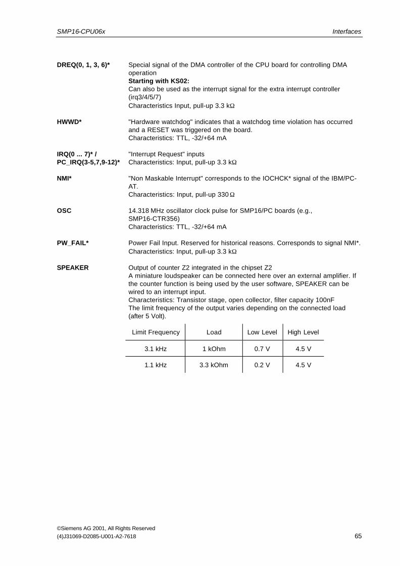
SMP16-CPU06x Interfaces
©Siemens AG 2001, All Rights Reserved(4)J31069-D2085-U001-A2-7618 65
DREQ(0, 1, 3, 6)* Special signal of the DMA controller of the CPU board for controlling DMAoperationStarting with KS02:Can also be used as the interrupt signal for the extra interrupt controller(irq3/4/5/7)Characteristics Input, pull-up 3.3 kΩ
HWWD* "Hardware watchdog" indicates that a watchdog time violation has occurredand a RESET was triggered on the board.Characteristics: TTL, -32/+64 mA
IRQ(0 ... 7)* /PC_IRQ(3-5,7,9-12)*
"Interrupt Request" inputsCharacteristics: Input, pull-up 3.3 kΩ
NMI* "Non Maskable Interrupt" corresponds to the IOCHCK* signal of the IBM/PC-AT.Characteristics: Input, pull-up 330 Ω
OSC 14.318 MHz oscillator clock pulse for SMP16/PC boards (e.g.,SMP16-CTR356)Characteristics: TTL, -32/+64 mA
PW_FAIL* Power Fail Input. Reserved for historical reasons. Corresponds to signal NMI*.Characteristics: Input, pull-up 3.3 kΩ
SPEAKER Output of counter Z2 integrated in the chipset Z2A miniature loudspeaker can be connected here over an external amplifier. Ifthe counter function is being used by the user software, SPEAKER can bewired to an interrupt input.Characteristics: Transistor stage, open collector, filter capacity 100nFThe limit frequency of the output varies depending on the connected load(after 5 Volt).
Limit Frequency Load Low Level High Level
3.1 kHz 1 kOhm 0.7 V 4.5 V
1.1 kHz 3.3 kOhm 0.2 V 4.5 V

Interfaces SMP16-CPU06x
©Siemens AG 2001, All Rights Reserved66 (4)J31069-D2085-U001-A2-7618
5.2 Drive Interfaces
5.2.1 Signals of the UNI-I/O Interface (SMP16-CPU065)
Below is the allocation of the UNI-I/O interface in accordance with V1.52 for hard disk and floppy diskdrives. X36 of the basic board of the SMP16-CPU065.
KS01 of the CPU
Connection a b c d e
1 DS1# DRVDEN1 MTR0# - GND
2 DS0# DRVDEN0 INDEX# SHDA# GND
3 MTR1# SDCS3# - - SDCS1#
4 DIR# SDA02 SDA00 SDIRQ SDA01
5 STEP# - - SDPU SDDACK#
6 WRDATA# - SDIOR# SDIOW# SIORDY
7 WGATE# SDDREQ - SDD15 SDD0
8 TRK0# SDD14 SDD1 SDD13 SDD12
9 WRTPRT# SDD8 DISK_RES# SDD7 SDD9
10 RDDATA# SDD6 SDD10 GND SDD5
11 HDSEL# SDD11 SDD4 GND GND
12 DSKCHG# SDD3 SDD2 GND GND
Note:HD: Secondary channel, max. of 2 drivesFD: Drive A, in acc. w. SWAP in Setup drive B (see chapter 9.1.4).
Starting with KS02 of the CPU
Connection a b c d e
1 DS0# DRVDEN1 MTR1# - GND
2 DS1# DRVDEN0 INDEX# SHDA# GND
3 MTR0# SDCS3# - - SDCS1#
4 DIR# SDA02 SDA00 SDIRQ SDA01
5 STEP# - - SDPU SDDACK#
6 WRDATA# - SDIOR# SDIOW# SIORDY
7 WGATE# SDDREQ - SDD15 SDD0
8 TRK0# SDD14 SDD1 SDD13 SDD12
9 WRTPRT# SDD8 DISK_RES# SDD7 SDD9
10 RDDATA# SDD6 SDD10 GND SDD5
11 HDSEL# SDD11 SDD4 GND GND
12 DSKCHG# SDD3 SDD2 GND GND
See also [2].
Note:HD: Secondary channel, max. of 2 drivesFD: Drive B, in acc. w. SWAP in Setup drive A (see chapter 9.1.4).

SMP16-CPU06x Interfaces
©Siemens AG 2001, All Rights Reserved(4)J31069-D2085-U001-A2-7618 67
5.2.2 Signals of the Rear Panel I/O Interface (SMP16-CPU066)
Below is the allocation of the rear panel I/O interface in accordance with own definition for hard diskand floppy disk drives. X38 of the basic board of the SMP16-CPU066.
Socket J2
Connection a b c d e
22 - - - - -
21 CPU GND - - -
20 CPU GND - - CPU
19 GND GND - - -
18 SDD(7) SDD(8) - - -
17 SDD(6) SDD(9) CPU CPU CPU
16 SDD(5) SDD(10) CPU - -
15 SDD(4) SDD(11) CPU CPU CPU
14 - - - INDEX# -
13 SDD(3) SDD(12) SDA0 FDMO0 MSEN0
12 SDD(2) SDD(13) SDA1 FDMO1 MSEN1
11 SDD(1) SDD(14) SDA2 FDWE# FDDS0#
10 SDD(0) SDD(15) SDCS1# WRDATA# FDDS1#
9 SDCS3# FDHEAD# FDSTEP#
8 SDIOW# SDDREQ SHDA# DSKCHG# FDDIR#
7 SDIOR# SDDACK# SPDIAG - TRK0#
6 - - SIORDY - FDWP#
5 DISKRES# - SDIRQ - RDDATA#
4 VIO - - - -
3 CPU GND CPU CPU CPU
2 CPU CPU CPU CPU CPU
1 CPU GND CPU CPU CPU
Note:HD: Secondary channel, max. of 2 drivesFD: Drive B, as per SWAP in Setup drive A (see chapter 9.1.4).
Before the drive interfaces of the rear-panel IO can be used, they must be activated in BIOS Setup(see chapter 9.1.9).

Interfaces SMP16-CPU06x
©Siemens AG 2001, All Rights Reserved68 (4)J31069-D2085-U001-A2-7618
5.2.3 Signals of the Hard Disk Interface (40-Pin)
This interface can be used to connect two hard disk drives to the primary EIDE channel. X6 of theSMP16 expansion board.
Connection Signal Connection Signal
1 DISK_RES* 2 GND
3 PDD7 4 PDD8
5 PDD6 6 PDD9
7 PDD5 8 PDD10
9 PDD4 10 PDD11
11 PDD3 12 PDD12
13 PDD2 14 PDD13
15 PDD1 16 PDD14
17 PDD0 18 PDD15
19 GND 20 -
21 PDDREQ 22 GND
23 PDIOW* 24 GND
25 PDIOR* 26 GND
27 PIORDY 28 Cable Select
29 PDDACK* 30 GND
31 IREQ14 32 -
33 PDA01 34 PDIAG*
35 PDA00 36 PDA02
37 PDCS1* 38 PDCS3*
39 PHDA* 40 GND
Note:Plug connector X6/X7 can be used to connect a maximum of 2 drives.

SMP16-CPU06x Interfaces
©Siemens AG 2001, All Rights Reserved(4)J31069-D2085-U001-A2-7618 69
5.2.4 Signals of the Hard Disk Interface (44-Pin)
This interface can be used to connect EIDE flash disks, for example. X7 of the SMP16 expansionboard.
Connection Signal Connection Signal
1 DISK_RES* 2 GND
3 PDD7 4 PDD8
5 PDD6 6 PDD9
7 PDD5 8 PDD10
9 PDD4 10 PDD11
11 PDD3 12 PDD12
13 PDD2 14 PDD13
15 PDD1 16 PDD14
17 PDD0 18 PDD15
19 GND 20 -
21 PDDREQ 22 GND
23 PDIOW* 24 GND
25 PDIOR* 26 GND
27 PIORDY 28 Cable Select
29 PDDACK* 30 GND
31 IREQ14 32 -
33 PDA01 34 PDIAG*
35 PDA00 36 PDA02
37 PDCS1* 38 PDCS3*
39 PHDA* 40 GND
41 VCC (motor) 42 VCC (logic)
43 GND 44 -
Note:Plug connector X6/X7 can be used to connect a maximum of 2 drives.

Interfaces SMP16-CPU06x
©Siemens AG 2001, All Rights Reserved70 (4)J31069-D2085-U001-A2-7618
5.2.5 Signals of the Floppy Disk Interface (34-Pin)
34-pin strip, TTL level. X8 of the SMP16 expansion board.
Connection Signal Connection Signal
1 GND 2 DENSEL
3 GND 4 -
5 GND 6 DRATE
7 GND 8 INDEX*
9 GND 10 MTR0*
11 GND 12 DS1*
13 GND 14 DS0*
15 GND 16 MTR1*
17 GND 18 DIR*
19 GND 20 STEP*
21 GND 22 WRDATA*
23 GND 24 WGATE*
25 GND 26 TRK0*
27 GND 28 WRTPRT*
29 GND 30 RDDATA*
31 GND 32 HDSEL*
33 GND 34 DSKCHG*
Note:FD: Drive A, in acc. w. SWAP in Setup drive B (see chapter 9.1.3).

SMP16-CPU06x Interfaces
©Siemens AG 2001, All Rights Reserved(4)J31069-D2085-U001-A2-7618 71
5.3 Front Plate Interfaces
5.3.1 USB Bus Interfaces
CPU
Pin No. Meaning
1 VCC (5 Volt) 1
2 USB1–
3 USB1+
4 GND
AGP board
Pin No. Meaning
1 VCC (5 Volt) Fehler! Textmarke nicht definiert.
2 USB2–
3 USB2+
4 GND
5.3.2 Signals of the Keyboard Interface
The keyboard socket is also assigned to the signals of the mouse interface. Both devices can beconnected when a Y adapter is used.
Connection Signal
1 KBDAT
2 MSDAT
3 GND
4 VCC (5 Volt) Fehler! Textmarke nicht definiert.
5 KBDCLK
6 MSCLK
1 VCC filtered and protected with 1 A fuse (0.165 Ohm internal solid state resistance)!

Interfaces SMP16-CPU06x
©Siemens AG 2001, All Rights Reserved72 (4)J31069-D2085-U001-A2-7618
5.3.3 Signals of the Serial Interfaces - COM A / COM B
Allocation of COM A/COM B; sub D, 9-pin pin; V24 level
Connection Signal Meaning Connection Signal Meaning
1 DCD Receiving signal level 6 DSR Ready for operation
2 RXD Receiving data 7 RTS Enable sending portion
3 TXD Sending data 8 CTS Ready to send
4 DTR Terminal ready for operation 9 RI Arriving call
5 GND Operating ground -
5.3.4 Signals of the LAN Interface (RJ45)
Allocation of the 8-pin western socket as per IEEE 802.3 (100/10BASE-TX)
Connection Designation Explanation
1 Tx+ Transmit data (pos.)2 Tx- Transmit data (neg.)3 Rx+ Receive data (pos.)
4 PD5 PD
Connected with pin 5,Terminating resistance, 75 Ohm
6 Rx- Receive data (neg.)
7 PD8 PD
Connected with pin 8,Terminating resistance, 75 Ohm

SMP16-CPU06x Interfaces
©Siemens AG 2001, All Rights Reserved(4)J31069-D2085-U001-A2-7618 73
5.3.5 Parallel Interface - LPT1
Allocation of the parallel interface is based on IEEE 1284. ECP + EPP 1.9 is set as default in BIOSSetup (see chapter 9.1.9). DMA channel 1 is used for this.
Allocation of LPT1, 25-pin sub D socket, TTL level
Standard printer port
Connection Signal Connection Signal
1 STROBE* 14 AUTOFD*
2 LPTDAT(0) 15 ERROR*
3 LPTDAT(1) 16 INIT*
4 LPTDAT(2) 17 SLCTIN*
5 LPTDAT(3) 18 GND
6 LPTDAT(4) 19 GND
7 LPTDAT(5) 20 GND
8 LPTDAT(6) 21 GND
9 LPTDAT(7) 22 GND
10 ACK* 23 GND
11 BUSY 24 GND
12 PE 25 GND
13 SELECT
Enhanced-capability port
Connection Signal Connection Signal
1 WRITE 14 DSTRB
2 LPTDAT(0) 15 Reserved
3 LPTDAT(1) 16 Reserved
4 LPTDAT(2) 17 ASTRB
5 LPTDAT(3) 18 GND
6 LPTDAT(4) 19 GND
7 LPTDAT(5) 20 GND
8 LPTDAT(6) 21 GND
9 LPTDAT(7) 22 GND
10 INTR 23 GND
11 WAIT 24 GND
12 Reserved 25 GND
13 Reserved

Interfaces SMP16-CPU06x
©Siemens AG 2001, All Rights Reserved74 (4)J31069-D2085-U001-A2-7618
Enhanced capability port
Connection Signal Connection Signal
1 HOST_CLK 14 HOST_ACK
2 LPTDAT(0) 15 PERIPH_REQ
3 LPTDAT(1) 16 REVERSE_REQ
4 LPTDAT(2) 17 ECP_MODE
5 LPTDAT(3) 18 GND
6 LPTDAT(4) 19 GND
7 LPTDAT(5) 20 GND
8 LPTDAT(6) 21 GND
9 LPTDAT(7) 22 GND
10 PERIPH_CLK 23 GND
11 PERIPH_ACK 24 GND
12 ACK_REVERSE 25 GND
13 XFLAG
5.3.6 CRT/LVDS Connection
Allocation of the CRT/LVDS interface, sub D, 15-pin socket, high density
Description
PIN CRT LVDS
1 RED Tx1-
2 GREEN Tx2+
3 BLUE Tx3-
4 NB TxCLK-
5 GND GND
6 GND Tx0-
7 GND Tx1+
8 GND Tx2+
9 VCC VCC
10 NC TxCLK+
11 NC Tx0+
12 DDCDAT DDCDAT
13 HSYNC ENAVDD
14 VSYNC Tc3+
15 DDCCLK DDCCLK
Note:Starting with KS03 of the AGP module, the standard setting is "CRT-only" (see chapter 3.6).

SMP16-CPU06x Interfaces
©Siemens AG 2001, All Rights Reserved(4)J31069-D2085-U001-A2-7618 75
5.3.7 PanelLink Connection
Allocation of the PanelLink interface, 26-pin, HD socket strip
Can be used starting with KS02
PIN Description PIN Description
1 GND 14 GND
2 Tx2+ 15 P12_S (12Volt)
3 Tx2 shield 16 P12_S (12Volt)
4 Tx2- 17 VCC_S (5 Volt)
5 Tx1+ 18 VCC_S (5 Volt)
6 Tx1 shield 19 GND
7 Tx1- 20 RFU
8 Tx0+ 21 NC
9 Tx0 shield 22 VCC3_S (3.3 Volt)
10 Tx0- 23 VCC3_S (3.3 Volt)
11 TxC+ 24 RFU
12 TxC shield 25 RFU
13 TxC- 26 GND
Note:Starting with KS03 of the AGP module, the standard setting is "CRT-only" (see chapter 3.6).
Warning
KS01 of the SMP16-CPU065 did not offer the PanelLink interface. The pin allocationwas redefined for KS02. It no longer agrees with the allocation of KS01.

Commissioning SMP16-CPU06x
©Siemens AG 2001, All Rights Reserved76 (4)J31069-D2085-U001-A2-7618
6 Commissioning
6.1 Wiring of the Power Supply
-12 V
0 V
+3.3 V
+5 V
+12 V
0 V
+3.3 V
+5 V
+3.3 VF
0 VF
PF*
ER*
SMP16-SV330
IPCI busbackplane orPS adapter
SMP16bus backplane
-12 V
0 V
+3.3 V
+5 V
+12 V
0 VF
+5 VF
Interrupt
0 V
+12 V
+5 VF
+5 V
0 VF
PF*
SMP16-SV531
-12 V
0 VF
+3.3 VF
ER*
Optional
nur bei IPCI 3,3 V I/O
Figure 6.1 Wiring of the power supply with SMP16-SV531 and SMP16-SV330
Note:If the sensor lines (VF) are not connected to the bus backplane, they must be connected directly tothe power supply on the appropriate potential (connections in the figure with a broken line).
Attention:If the ER* line between SMP16-SV531 and SMP16-SV330 is not wired, an overload on the 3.3 Vside may destroy the SMP16-SV330!

SMP16-CPU06x Commissioning
©Siemens AG 2001, All Rights Reserved(4)J31069-D2085-U001-A2-7618 77
6.2 Settings on the Hardware
The following figure shows the user-relevant connections on the configuration side of theSMP16-CPU06x and the setting elements in the presetting made at the factory before delivery.
S1
12
Heat dissipater
Pentium II Mobile Module
X2
X3
X36
SDRAM module
F1
F2
F4
Figure 6.2 Location of the connection and setting elements on the CPU basic board of the SMP16-CPU065
Fuses F2 and F4 must be inserted when the IPCI backplane is used without a 3.3 V power supply (VI/O = 3.3 V required).f the system has a 3.3 V power supply and it is wired, F2 and F4 must be removed.
Note:The values for the fuses are listed in chapter 6.5.

Commissioning SMP16-CPU06x
©Siemens AG 2001, All Rights Reserved78 (4)J31069-D2085-U001-A2-7618
S1
1
4
Heat dissipater
Pentium II Mobile Module
SDRAM module
F1
X2
X38
offon
Figure 6.3 Location of the connection and setting elements on the CPU basic board of theSMP16-CPU066
Switches S1-3 and S1-4 must be closed when the CPCI backplane is used without 3.3 V power (V I/O= 3.3 V required).If the system has 3.3 V power and this is wired, S1-3 and S1-4 must be open.
Note:The values for the fuses are listed in chapter 6.5.

SMP16-CPU06x Commissioning
©Siemens AG 2001, All Rights Reserved(4)J31069-D2085-U001-A2-7618 79
X6 X8
Pin 1 Pin 1X7
Pin 1
X1
X11
Pin 1
X12
Figure 6.4 SMP16 expansion board KS02
Note:The KS01 of the SMP16 expansion board did not have plug-in connectors for digital inputs/outputs!
X6 X8Pin 1 Pin 1 X7
Pin 1
X1
X11
Pin 1
X12
X4
X5
Figure 6.5 SMP16 expansion board, starting with KS03 with possible connection of the CPCI-MEM371/2 toX4/X5

Commissioning SMP16-CPU06x
©Siemens AG 2001, All Rights Reserved80 (4)J31069-D2085-U001-A2-7618
S1
12
123456
12345678
onoff
on
off
S2
S3
onoff
X11 X12
Pin 1 Pin 1
X14
X13
X7
F1VGA -BIOS
Figure 6.6 AGP graphics module
S2: Can be accessed from above. Must not be demounted.
S1/S3: Can be accessed after AGP board is demounted (switch between CRT ↔ LVDS)

SMP16-CPU06x Commissioning
©Siemens AG 2001, All Rights Reserved(4)J31069-D2085-U001-A2-7618 81
6.3 Deleting the CMOS Configuration
A gold capacitor briefly buffers (at least 1 hour) the function of the realtime clock and the Setup dataon the CMOS-RAM when a power failure occurs or the power is turned off.
Note:Due to the implementation of the CDT on the SMP16-CPU06x, the board cannot be put into anoriginal state by deleting the CMOS-RAM on the RTC. Not until the CDT in flash is also set to"invalid" by the modification described below does the CPU start up with "CMOS invalid." Otherwisethe data are copied from the CDT to CMOS.
Deleting CMOS:If you want to delete these data and start the system with the default values from BIOS or from theCMOS default table, you can speed up the discharging of the capacitor as shown below.
1. Remove the SMP16-CPU06x from the system rack.
2. Close switch S1.2.
3. Wait approx. 1 minute and open switch X1.2 again.
4. During the new start, a connection must be made between pin 2 and pin 12 on the LPT plugconnector (see chapter 3.1).
Attention:Do not operate the board when S1.1 and S1.2 are ON simultaneously!
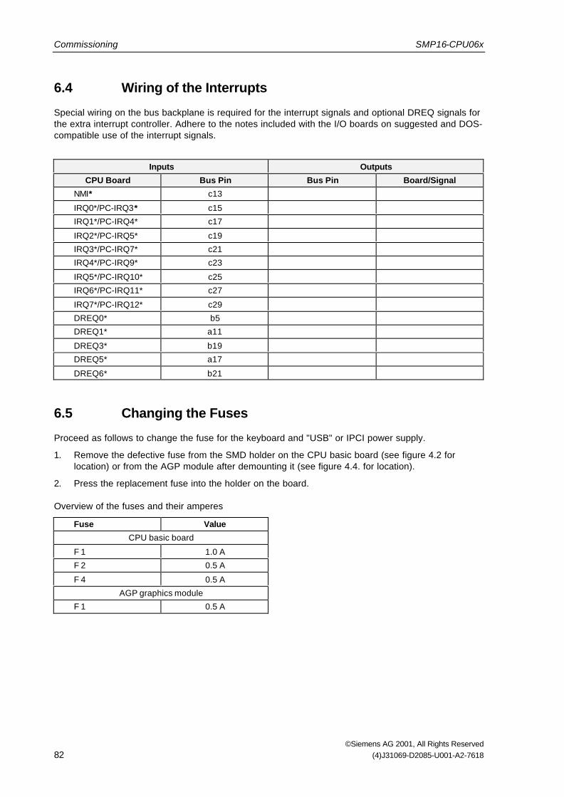
Commissioning SMP16-CPU06x
©Siemens AG 2001, All Rights Reserved82 (4)J31069-D2085-U001-A2-7618
6.4 Wiring of the Interrupts
Special wiring on the bus backplane is required for the interrupt signals and optional DREQ signals forthe extra interrupt controller. Adhere to the notes included with the I/O boards on suggested and DOS-compatible use of the interrupt signals.
Inputs Outputs
CPU Board Bus Pin Bus Pin Board/Signal
NMI* c13
IRQ0*/PC-IRQ3* c15
IRQ1*/PC-IRQ4* c17
IRQ2*/PC-IRQ5* c19
IRQ3*/PC-IRQ7* c21
IRQ4*/PC-IRQ9* c23
IRQ5*/PC-IRQ10* c25
IRQ6*/PC-IRQ11* c27
IRQ7*/PC-IRQ12* c29
DREQ0* b5
DREQ1* a11
DREQ3* b19
DREQ5* a17
DREQ6* b21
6.5 Changing the Fuses
Proceed as follows to change the fuse for the keyboard and "USB" or IPCI power supply.
1. Remove the defective fuse from the SMD holder on the CPU basic board (see figure 4.2 forlocation) or from the AGP module after demounting it (see figure 4.4. for location).
2. Press the replacement fuse into the holder on the board.
Overview of the fuses and their amperes
Fuse Value
CPU basic board
F 1 1.0 A
F 2 0.5 A
F 4 0.5 A
AGP graphics module
F 1 0.5 A

SMP16-CPU06x Commissioning
©Siemens AG 2001, All Rights Reserved(4)J31069-D2085-U001-A2-7618 83

Notes on Programming SMP16-CPU06x
©Siemens AG 2001, All Rights Reserved84 (4)J31069-D2085-U001-A2-7618
7 Notes on ProgrammingFirst, this chapter gives you an overview of the address areas of the board.
Later, information is given on programming the board (modifying the address areas, special registerand board functions).
7.1 Memory Address Areas
FFFF FFFFH
FFF0 0000H
3)
0010 0000H
000F FFFFH
256-kbyte system BIOS (imaged)
Internal board working storage
System BIOS
000A 0000H
Internal board working storage
0000 0000H
0009 FFFFHFlash memory
DRAM
SMP16 bus
SMP16 memory input/output and SMP16 memory 2)
768-kbyte user data
00F0 0000H
00FF FFFFHImaged SMP16 bus 1)
FFFC 0000H
4)
PCI memory area
1) "Enable Memory Hole" option must be enabled in Setup.2) LAN BIOS in system BIOS can be linked in or VGA BIOS and video memory, USB and any enabled SRAM
window.3) Depends on memory expansion
4) With Preboot Agent 0F0000H deactivated, otherwise 0E0000H
Figure 7.1 Memory Address Areas

SMP16-CPU06x Notes on Programming
©Siemens AG 2001, All Rights Reserved(4)J31069-D2085-U001-A2-7618 85
Allocation of the memory in lowest megabyte range based on Setup settings
Address SRAM Size 8/16K SRAM Size 32K Customer Application
EFFFFHEC000H
1. Preboot agent 4)
2. External BIOS extension
EBFFFH
E8000H
1. Preboot agent 4)
2. External BIOS extension
E7FFFH
E4000H
1. Preboot agent 4)
2. On-board SRAM 3)
3. External BIOS extension
E3FFFH
E0000H
1. Preboot agent 4)
2. On-board SRAM 3)
3. External BIOS extension
DFFFFHDC000H
1. On-board SRAM 3)
2. External BIOS extension
DBFFFH
D8000H
1. On-board SRAM 3)
2. External BIOS extension
D7FFFH
D4000H
1. On-board SRAM 3)
2. On-board LAN 2)
3. External BIOS extension
D3FFFH
D0000H
1. On-board SRAM 3)
2. USB1)
3. On-board LAN 2)
4. External BIOS extension
CFFFFH
CC000H
1. On-board SRAM 3)
2. USB1)
3. On-board LAN 2)
4. External BIOS extension
1. USB1)
2. On-board LAN 2)
3. External BIOS extension
CBFFFH
C8000H
1. VGA-BIOS > 32k2. USB1)
3. On-board LAN 2)
4. External BIOS extension
1. VGA-BIOS > 32k2. USB1)
3. On-board LAN 2)
4. External BIOS extension
C7FFFH
C0000H
1. VGA-BIOS 1. VGA-BIOS
BFFFFH
A0000H
128-k video memory
9FFFFH
0H
640-k program memory
1) If "USB-Keyboard Support" enabled in Setup
2) If "Boot from LAN first" enabled in Setup3) If "Onboard SRAM" enabled in Setup
4) If "Award Preboot Agent" and "Agent after Boot" enabled in Setup
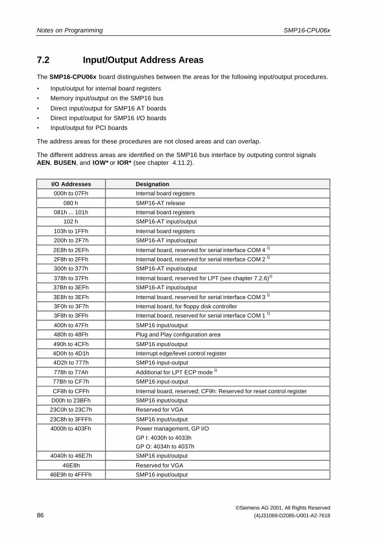
Notes on Programming SMP16-CPU06x
©Siemens AG 2001, All Rights Reserved86 (4)J31069-D2085-U001-A2-7618
7.2 Input/Output Address Areas
The SMP16-CPU06x board distinguishes between the areas for the following input/output procedures.
• Input/output for internal board registers
• Memory input/output on the SMP16 bus
• Direct input/output for SMP16 AT boards
• Direct input/output for SMP16 I/O boards
• Input/output for PCI boards
The address areas for these procedures are not closed areas and can overlap.
The different address areas are identified on the SMP16 bus interface by outputing control signalsAEN, BUSEN, and IOW* or IOR* (see chapter 4.11.2).
I/O Addresses Designation
000h to 07Fh Internal board registers
080 h SMP16-AT release
081h ... 101h Internal board registers
102 h SMP16-AT input/output
103h to 1FFh Internal board registers
200h to 2F7h SMP16-AT input/output
2E8h to 2EFh Internal board, reserved for serial interface COM 4 1)
2F8h to 2FFh Internal board, reserved for serial interface COM 2 1)
300h to 377h SMP16-AT input/output
378h to 37Fh Internal board, reserved for LPT (see chapter 7.2.6)1)
37Bh to 3EFh SMP16-AT input/output
3E8h to 3EFh Internal board, reserved for serial interface COM 3 1)
3F0h to 3F7h Internal board, for floppy disk controller
3F8h to 3FFh Internal board, reserved for serial interface COM 1 1)
400h to 47Fh SMP16 input/output
480h to 48Fh Plug and Play configuration area
490h to 4CFh SMP16 input/output
4D0h to 4D1h Interrupt edge/level control register
4D2h to 777h SMP16 input-output
778h to 77Ah Additional for LPT ECP mode 1)
77Bh to CF7h SMP16 input-output
CF8h to CFFh Internal board, reserved; CF9h: Reserved for reset control register
D00h to 23BFh SMP16 input/output
23C0h to 23C7h Reserved for VGA
23C8h to 3FFFh SMP16 input/output
4000h to 403Fh Power management, GP I/O
GP I: 4030h to 4033hGP O: 4034h to 4037h
4040h to 46E7h SMP16 input/output
46E8h Reserved for VGA
46E9h to 4FFFh SMP16 input/output

SMP16-CPU06x Notes on Programming
©Siemens AG 2001, All Rights Reserved(4)J31069-D2085-U001-A2-7618 87
I/O Addresses Designation
5000h to 500Fh SMB (system management bus)
5010h to 7FDFh SMP16 input/output
7FE0h to 7FE7h ASBIC port master subrack 2)
7FE8h to 7FEFh ASBIC port slave subrack 2)
7FF0h to 7FF7h ASBIC port bus coupler 2)
7FF8h to DFFFh SMP16 input/output
E000h to E01Fh LAN controller
E020h to E3FFh SMP16 input/output
E400h to E41Fh USB controller
E420h to EFFFh SMP16 input/output
F000h to F00Fh Bus master IDE
F010h to FFFFh SMP16 input/output
1) Depends on setting in Setup
2) The addresses for the bus coupler must only be reserved if the system actually has a bus coupler. Theaddresses of the ASBIC of the slave subrack boards must only be reserved if ASBIC boards are actuallyused in the slave subrack.When boards which image themselves in the I/O address area every 100h are used, I/O address areas E0to E7, E8 to EF and F0 to F7 cannot be used for boards.
Note:When planning the system, remember to also include the addresses which the graphics board needs(see chapter 4.6).
BIOS automatically assigns PCI I/O addresses in the area E000h to FFFFh. These addresses can nolonger be accessed on the SMP16 bus.

Notes on Programming SMP16-CPU06x
©Siemens AG 2001, All Rights Reserved88 (4)J31069-D2085-U001-A2-7618
7.2.1 Input/Output for Internal Board Registers
The input/output address area is reserved for internal board functions in the area from 000h to 1FFh(exception: addresses 80h for POST outputs and 102h for VGA register are output on the SMP16-ATbus).
If necessary and not already documented in the standard literature on AT systems, the registers willbe explained after the table which follows.
The following addresses are used for internal board registers.
Addresses Input/Output Unit
000 to 00Fh 8237A-compatible DMA controller for 8-bit transfers
020h to 021h020h021h
Interrupt controllerCommand portEnable mask
040h to 043h040h041h042h043h
8254-compatible counterCounter Z0, system clock
Counter Z1, RAM refresh controlCounter Z2, loudspeaker
Control register for all counters
060 h Keyboard data port (scan code, 8742-compatible)
061 h System status bits
Bit Meaning When Bit =1 Bit Meaning When Bit =1
0 Enable counter 2 gate 4 Refresh tick
1 Enable loudspeaker 5 Counter 2 output
2 Disable PCI SERR 6 I/O channel NMI status
3 Disable I/O channel NMI 7 SERR NMI status
064 h Keyboard command port (8742-compatible)
070h071h
NMI enable, realtime clock and CMOS-RAM:Bit 7: General NMI enable;Bit 6 to 0: Address of the realtime clock
Data
080 h Only write: POST outputs
080h ... 087h DMA page register and RAM refresh
092 h Port 92; quick GATE A20 switchover, quick software processor reset
0A0h ... 0A1h Slave interrupt controller
0C0h to 0DFh 8237A-compatible DMA controller for 16-bit transfers
0F0h to 0FFh Arithmetic coprocessor
102 h Exception for SMP16 VGA card: This address is output on the SMP16 bus.
130 h Extra interrupt controller command port
131 h Extra interrupt controller enable mark
132 h 8-bit register as memory location
133 h INTA for extra interrupt controller
134h to 137h134h135h136h137h
Additional counter, 8254-compatible counterCounter ZZ0Counter ZZ1Counter r ZZ2
Control register for all counters
138 h Port 0
139 h Port 1
13Ah DI/DQ control register, state of INTA state machine

SMP16-CPU06x Notes on Programming
©Siemens AG 2001, All Rights Reserved(4)J31069-D2085-U001-A2-7618 89
Addresses Input/Output Unit
13Bh Single enable: Clock pulses and gates of the extra counters, clock pulses for SMP16 bus
13Ch Ready timing, port 0: Bits 3 to 5 on counter gates, bits 0 to 2 on counter clock pulses
170h ...177h EIDE channel 2
178 h Control register 1
179 h Control register 2
17Ah SRAM base address
17Bh SMP – INTA
17Ch Control register 3
17Dh Control register 4
17Eh Watchdog enable register
17Fh Watchdog trigger register
1F0h to 1F7h EIDE channel 1
7.2.1.1 On-Board Controller Chips
Extra interrupt controller 82C59
The extra 82C59 interrupt controller is addressed with addresses 130h and 131h. It is initialized asfollows during startup: (edges triggered; one master, no slaves; vector 80h; all interrupts masked.
• Address 130h: ICW1 = 11h
• Address 131h: ICW2 = 80h ICW3 = 00h ICW4 = 01h OCW1 = FFh
• Address 133h: Trigger INTA for the extra interrupt controller
Note:When the function is used to cascade the extra interrupt controller on the SMP16 bus, this interruptcontroller must be programmed in BUFFERED/MASTER mode. Bits 2 and 3 must always be set to 1in ICW4 (address 131h) of the interrupt controller.
Cascading the extra interrupt controller on the SMP16 bus
The CAS lines of the extra interrupt controller are connected to the SMP16 bus. The DACK0* (CAS0),DACK5* (CAS1), and DACK6* (CAS2) signals are used for this. In addition, the Z_INTA signal isavailable on DACK1* for the extra interrupt controller.
Prerequisites: cascading is enabled (see chapter 7.2.1.7) and the extra interrupt controller isprogrammed in the mode described above. The DMA channels can then not be used.
The interrupt output of the extra interrupt controller must be routed to one of the PC-IRQs (see chapter7.2.1.7).

Notes on Programming SMP16-CPU06x
©Siemens AG 2001, All Rights Reserved90 (4)J31069-D2085-U001-A2-7618
Initialization of the extra interrupt controller in buffered master mode
• Address 130h: ICW1 = 11h
• Address 131h: ICW2 = 80h Interrupt vector base address ICW3 = xxxxx000b Program interrupt input
of the slave controller ICW4 = 0Dh Buffered master mode OCW1 = xxh Program mask
The following diagram shows how the interrupt routine can be looped in to the interrupt.
CPU065 interrupt service routine
Int Service Routine
RET
User program
INT
...
...
...
MOV DX,133H
IN AL, DX
IN AL, DXSHL AX, 2
CALL DWORD PTR[BX]
.......
1. INTA-pulse2. INTA-pulse
Generate interrupt address
Load INTA port address
MOV BX, AX
MOV AH, 0H
IRET
...
Initialization of extra interrupt controller, set bit CAB_EN
CAS signalsactive
SMP16-Bus
Data driveractive (read)
Interrupt vectorcan be read.
Figure 7.2 Looping in an interrupt routine to the interrupt

SMP16-CPU06x Notes on Programming
©Siemens AG 2001, All Rights Reserved(4)J31069-D2085-U001-A2-7618 91
Additional counter chip 82C54
The 82C54 additional counter chip is clock pulsed with 8.33 or 14.318 MHz and is addressed viaaddresses 134h to 137h.
• Address 134h = Counter0_Count
• Address 135h = Counter1_Count
• Address 136h = Counter2_Count
• Address 137h = Control_Word_Counter0_2
The gate inputs of the three additional counters can be enabled together. Timers ZZ0 and ZZ1 can becascaded. The outputs are connected to the interrupt matrix via the extra interrupt controller (seefigure 2.3).BIOS initializes the counters (data 2 consecutive bytes, mode 3, binary, counter value = 0h). Gate andclock pulse inputs are inactive after the reset.
Starting with KS02 of the SMP16 expansion board, the clock pulse and gate inputs of the additionalcounter chip can also be enabled separately (see chapter 7.2.1.5)In addition, you can now use six digital inputs of port 0 as gate and clock pulse inputs (see chapter7.2.1.6).

Notes on Programming SMP16-CPU06x
©Siemens AG 2001, All Rights Reserved92 (4)J31069-D2085-U001-A2-7618
7.2.1.2 Overview of the Control Register
Allocation of SMP16 register
Attention:Do not change the contents of the reserved bits! (Set by BIOS)
Note:Registers 138h to 13Ch are not available until KS02 of the SMP16 expansion board.

SMP16-CPU06x Notes on Programming
©Siemens AG 2001, All Rights Reserved(4)J31069-D2085-U001-A2-7618 93
7.2.1.3 Digital Inputs/Outputs
Starting with KS02, the SMP16-CPU06x is equipped with two digital ports (level of max. of 5 V TTL).These ports can be parameterized as inputs or outputs. Both ports can only be addressed with 8-bitaccesses.
Port 0: Digital inputs/outputs, 138h: r/w
Bit 7 6 5 4 3 2 1 0 Meaning
Status of port 0Input
Read Digital inputs DI 00 to 07Write Set internal register
OutputRead Output value can be read back.Write Digital outputs DQ 00 to 07
Port 0 can be used instead to address the additional counter chip (see chapter 7.2.1.6).
Port 0: Digital clock-pulse and gate inputs of the extra counter, 138h: r/w
Bit 7 6 5 4 3 2 1 0 Meaning
Clock pulse input ZZ0
Clock pulse input ZZ1
Clock pulse input ZZ1
Gate input ZZ0
Gate input ZZ0
Gate input ZZ0
DI 06
DI 07
Port 1: Digital inputs/outputs, 139h: r/w
Bit 7 6 5 4 3 2 1 0 Meaning
Status of port 1Input
Read Digital inputs DI 10 to 17Write Set internal register
OutputRead Output value can be read back.Write Digital outputs DQ 10 to 17

Notes on Programming SMP16-CPU06x
©Siemens AG 2001, All Rights Reserved94 (4)J31069-D2085-U001-A2-7618
7.2.1.4 DI/DQ Control Register: (R/W, Address 13Ah)
The two digital ports can be set up with this register. Bit 7 of this register also indicates the status ofthe INTA logic for the extra interrupt controller.
Meaning of the bits
Bit 7 6 5 4 3 2 1 0 Meaning
0 (default) = Port 0 input1 = Port 0 output
0 = Port 0 high-ohmic1 (default) = Port 0 enabled
0 (default) = Port 1 input1 = Port 1 output
0 = Port 1 high-ohmic1 (default) = Port 1 enabled
Reserved
Status of the state machine for the cascaded interrupts onthe SMP16 bus (see chapter 7.2.1.7)0 (default) = Basic state1 = First INTA executed
Attention:If a port is reprogrammed to output, the last value stored in register 138/9h is triggered (when theport is also enabled at the same time).
Note:BIOS programs the two ports as inputs.
7.2.1.5 Additional Control Register 1 (R/W, Address 13Bh)
This control register can be used to expand the functions of the additional counter chip. In addition tothe general enable of the additional counters (see chapter 7.2.1.12), the clock pulse and gate inputs ofthe three counters can be addressed separately.
In addition, the two clock pulses on the SMP16 bus can be enabled separately (see also chapter7.2.1.7).
Attention:This functionality can only be used when the additional counters and the clock pulses for the SMP16bus have all been enabled (general enable).
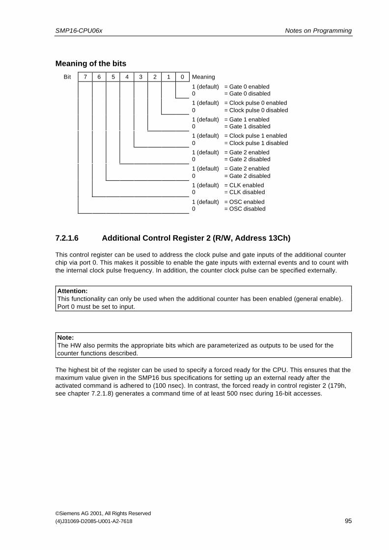
SMP16-CPU06x Notes on Programming
©Siemens AG 2001, All Rights Reserved(4)J31069-D2085-U001-A2-7618 95
Meaning of the bits
Bit 7 6 5 4 3 2 1 0 Meaning
1 (default) = Gate 0 enabled0 = Gate 0 disabled
1 (default) = Clock pulse 0 enabled0 = Clock pulse 0 disabled
1 (default) = Gate 1 enabled0 = Gate 1 disabled
1 (default) = Clock pulse 1 enabled0 = Clock pulse 1 disabled
1 (default) = Gate 2 enabled0 = Gate 2 disabled
1 (default) = Gate 2 enabled0 = Gate 2 disabled
1 (default) = CLK enabled0 = CLK disabled
1 (default) = OSC enabled0 = OSC disabled
7.2.1.6 Additional Control Register 2 (R/W, Address 13Ch)
This control register can be used to address the clock pulse and gate inputs of the additional counterchip via port 0. This makes it possible to enable the gate inputs with external events and to count withthe internal clock pulse frequency. In addition, the counter clock pulse can be specified externally.
Attention:This functionality can only be used when the additional counter has been enabled (general enable).Port 0 must be set to input.
Note:The HW also permits the appropriate bits which are parameterized as outputs to be used for thecounter functions described.
The highest bit of the register can be used to specify a forced ready for the CPU. This ensures that themaximum value given in the SMP16 bus specifications for setting up an external ready after theactivated command is adhered to (100 nsec). In contrast, the forced ready in control register 2 (179h,see chapter 7.2.1.8) generates a command time of at least 500 nsec during 16-bit accesses.

Notes on Programming SMP16-CPU06x
©Siemens AG 2001, All Rights Reserved96 (4)J31069-D2085-U001-A2-7618
Meaning of the bits
Bit 7 6 5 4 3 2 1 0 Meaning
0 (default) = Internal clock pulse input ZZ01 = Clock pulse input ZZ0 on port 0, bit 0
0 (default) = Internal clock pulse input ZZ11 = Clock pulse input ZZ1 on port 0, bit 1
0 (default) = Internal clock pulse input ZZ21 = Clock pulse input ZZ3 on port 0, bit 2
0 (default) = Internal gate input ZZ01 = Gate input ZZ0 on port 0, bit 3
0 (default) = Internal gate input ZZ11 = Gate input ZZ1 on port 0, bit 4
0 (default) = Internal gate input ZZ21 = Gate input ZZ2 on port 0, bit 5
Reserved
0 (default) = Forced ready deactivated1 = Forced ready activated
7.2.1.7 Control Register 1 (R/W, Address 178h)
An extra interrupt controller has been added to the SMP16 board to expand the PC-compatibleinterrupt system.
This interrupt controller (82C59) increases the number of interrupts which can be fed in over theSMP16 bus by a total of 7 interrupts. The output of the extra interrupt controller is routed for this to aPC interrupt.
Meaning of the bits
Bit 7 6 5 4 3 2 1 0
0 0 0 = Disabled0 0 1 = IRQ30 1 0 = IRQ50 1 1 = IRQ71 0 0 = IRQ91 0 1 = IRQ101 1 0 = IRQ111 1 1 = IRQ12
ReservedStarting with KS02: Cascading of extra interrupt controller
0 (default) = Disabled1 = Enabled
Reserved
Reserved
Clock pulses on SMP16 bus 1)
0 = Enabled1 = Disabled
SMP16 bus interface including clock pulses 1)
0 = Enabled1 = Disabled
1) Depends on setting in Setup

SMP16-CPU06x Notes on Programming
©Siemens AG 2001, All Rights Reserved(4)J31069-D2085-U001-A2-7618 97
7.2.1.8 Control Register 2 (R/W, Address 179h)
This register can be used to enable or disable memory address areas for the SMP16 bus.
Note:When 16-bit accesses are set, the I/O board must actually use word accesses. If the E segment isenabled, remember that the code of the Preboot Agent may be activated there. This means accesseswill not reach the SMP16 bus.
Accesses to the top 4 kbytes of the topmost enabled block are processed as memory inputs/outputs(see chapter 6.2.5).
Meaning of the bits of the SMP16 control register
Bit 7 6 5 4 3 2 1 0 Meaning for SMP16 memory accesses
Memory area 000D 0000h to 000D 7FFFh(MEM0)0 = Enabled 1)
1 = Enabled, 16-bit accesses 2)
Reserved
Memory area 000D 8000h to 000D FFFh(MEM2)0 = Enabled 1)
1 = Enabled, 16-bit accesses 2)
READY signal for SMP16 bus accesses
0 = Don't force READY1 = Force READY (command time of at least 500 nsec.)
Memory area 000E 0000h to 000E 7FFFh(MEM4, MEM5)0x = Disabled10 = Enabled 1)
11 = Enabled, 16-bit accesses 2)
Memory area 000E 8000h to 000E FFFh(MEM6, MEM7)0x = Disabled10 = Enabled 1)
11 = Enabled, 16-bit accesses 2)
1) I/O can activate MEMCS16* to request 16-bit accesses from the CPU.
2) The CPU board activates the MEMCS16* signal independently of the I/O.
Default setting
The default value of the SMP16 control register is 000000X0b. This results in the followingassignments.
Address Area Default Assignment
000E 8000h to 000E FFFFh On-board
000E 0000h to 000E 7FFFh On-board
000D 8000h to 000D FFFFh SMP16 bus 1)
000D 0000h to 000D 7FFFh SMP16 bus
1) MMIO* active for 000D F000 to 000D FFFFh

Notes on Programming SMP16-CPU06x
©Siemens AG 2001, All Rights Reserved98 (4)J31069-D2085-U001-A2-7618
7.2.1.9 SRAM Address Register (R/W, Address 17Ah)
The SMP16 board offers a 128-kbyte SRAM. This maximum of 128 kbytes can be shadowed byregister in various address areas. The length and enable are handled by register 17Dh (see chapter7.2.1.12). The presetting in BIOS Setup offers a limited selection (see chapter 9.1.10).
Meaning of the bits
Bit 7 6 5 4 3 2 1 0 Meaning
Setting the SRAM base address
00000h
1FFFFh
A0000h
EFFFFh
SRAM base (e.g., R17A = D8h)
D8000h
18000h
SRAMsize (e.g.,R17D(7:5) = 001b (4 kbytes)) 4)
128-Kbyte SRAM
1MByte SMP16 memory
B0000h
C0000h
D0000h
E0000h
D8FFFh
1)
1) :Only available if no VGA/AGP graphics in system
2)
2) : Only available is Preboot Agent not installed
18FFFh
00000h
3)
3) : Access to this memory area only via activated memory hole (at F00000h to FFFFFFh)4) : Size of SRAM area due to the incrementation of the base address
5)
5) :SRAM address 0h only accessible in 128-Kbyte increments
.
.
.

SMP16-CPU06x Notes on Programming
©Siemens AG 2001, All Rights Reserved(4)J31069-D2085-U001-A2-7618 99
7.2.1.10 INTA* Generation (Read Only, Address 17Bh)
Cascaded interrupts on the SMP16 bus can be handled by this register. This requires a separateinterrupt controller board (e.g., SMP16-SFT304) on the SMP16 bus. With the SMP16-CPU06x, anSMP interrupt must be used for the interrupt request of this controller.
When the "INTA* generation" register is read on the SMP16-CPU06x, the interrupt-acknowledgesignal is output on the INTA* SMP16 line (connected-through line a23 on the SMP16 bus). When aninterrupt control board outputs an interrupt vector, this vector is read. It can be processed as shownbelow.
The following diagram shows how the interrupt routine can be looped in to the interrupt.
Interruptservice routine, CPU065
Int Service Routine
RET
User program
INT
...
...
...
MOV DX,17BHIN AL, DX
IN AL, DXSHL AX, 2
CALL DWORD PTR[BX]
.......
1st INTA pulse2nd INTA pulse
Generate interrupt address
Load INTA port address
MOV BX, AX
MOV AH, 0H
IRET...
Figure 7.3 Looping in an interrupt routine to the interrupt
Attention:Depending on which IDE channel is enabled (see chapter 9.1.9), connected-through signal IRQ* (seechapters 5.1.3 and 5.1.4) of the SMP16 bus is placed on PC-IRQ14/15.When both IDE channels are activated, this interrupt cannot be used.If only the secondary IDE channel is activated, the IRQ* signal arrives at PC-IRQ14.If only the primary IDE channel is active, "Legacy ISA" must also be activated in Setup for IRQ15(see chapter 9.1.7). If not, the IRQ* signal will not arrive at PC-IRQ15. The same applies when bothIDE channels are deactivated.

Notes on Programming SMP16-CPU06x
©Siemens AG 2001, All Rights Reserved100 (4)J31069-D2085-U001-A2-7618
7.2.1.11 Control Register 3 (R/W, Address 17Ch)
Meaning of the bits
Bit 7 6 5 4 3 2 1 0 Meaning
LED10 User-defined function (see chapter 7.2.3) 1)
1: Reserved for primary HD channel
LED 2
0 User-defined function (see chapter 7.2.3) 1)
1: Reserved for secondary HD channel
LED3
0 User-defined function (see chapter 7.2.3) 1)
1: Reserved for functions of the LAN interface
LED40 User-defined function (see chapter 7.2.3) 1)
1: Reserved for functions of the LAN interface
Reserved
1) Presetting in Setup possible (see chapter 9.1.10)
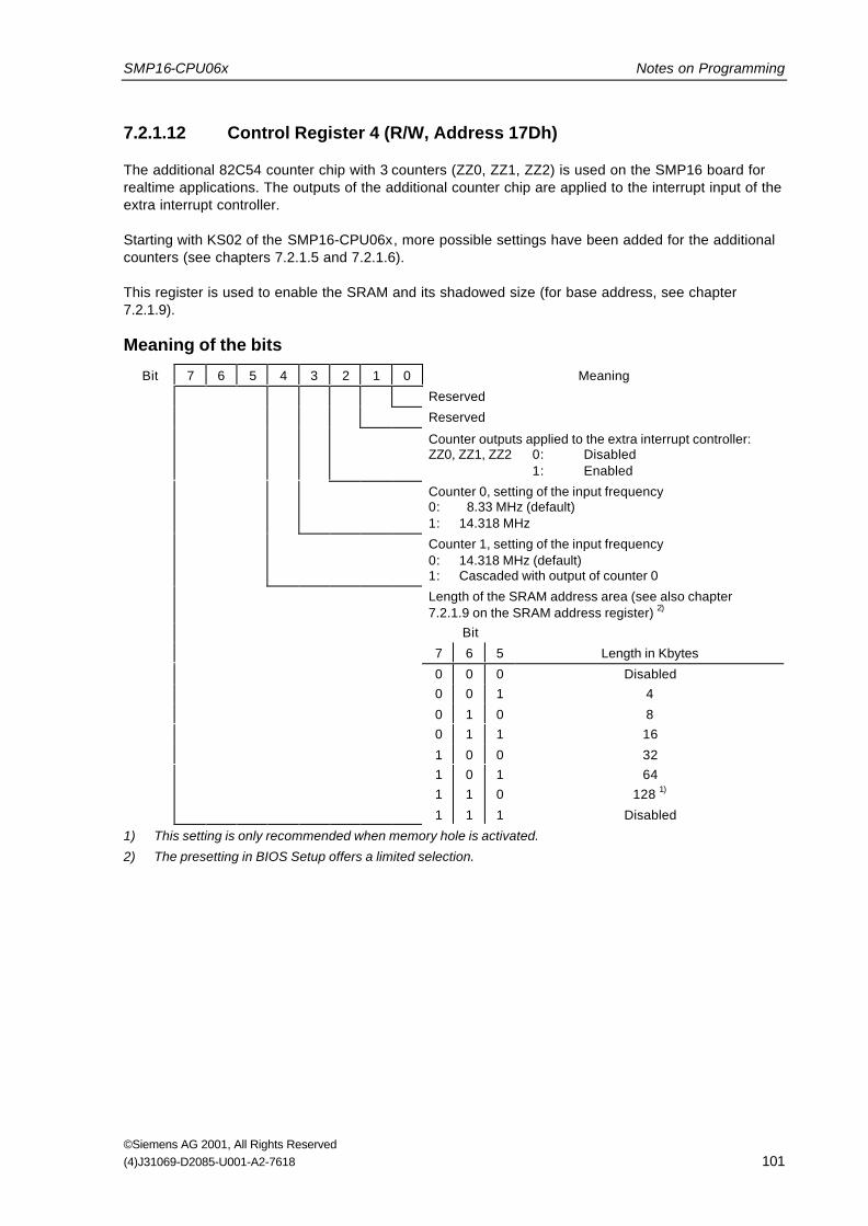
SMP16-CPU06x Notes on Programming
©Siemens AG 2001, All Rights Reserved(4)J31069-D2085-U001-A2-7618 101
7.2.1.12 Control Register 4 (R/W, Address 17Dh)
The additional 82C54 counter chip with 3 counters (ZZ0, ZZ1, ZZ2) is used on the SMP16 board forrealtime applications. The outputs of the additional counter chip are applied to the interrupt input of theextra interrupt controller.
Starting with KS02 of the SMP16-CPU06x, more possible settings have been added for the additionalcounters (see chapters 7.2.1.5 and 7.2.1.6).
This register is used to enable the SRAM and its shadowed size (for base address, see chapter7.2.1.9).
Meaning of the bits
Bit 7 6 5 4 3 2 1 0 Meaning
Reserved
Reserved
Counter outputs applied to the extra interrupt controller:ZZ0, ZZ1, ZZ2 0: Disabled
1: Enabled
Counter 0, setting of the input frequency0: 8.33 MHz (default)1: 14.318 MHz
Counter 1, setting of the input frequency0: 14.318 MHz (default)1: Cascaded with output of counter 0
Length of the SRAM address area (see also chapter7.2.1.9 on the SRAM address register) 2)
Bit
7 6 5 Length in Kbytes
0 0 0 Disabled0 0 1 4
0 1 0 80 1 1 16
1 0 0 321 0 1 641 1 0 128 1)
1 1 1 Disabled
1) This setting is only recommended when memory hole is activated.
2) The presetting in BIOS Setup offers a limited selection.

Notes on Programming SMP16-CPU06x
©Siemens AG 2001, All Rights Reserved102 (4)J31069-D2085-U001-A2-7618
7.2.1.13 Watchdog Enable Register (R/W, Address 17Eh)
Meaning of the bits
Bit 7 6 5 4 3 2 1 0 Meaning
Watchdog enable bit (WDE)0: Watchdog circuit is disabled.1: Watchdog circuit is enabled.
Reserved
Reserved
Bit5 4 3 Scaler, watchdog time
0 0 0 94 msec (def.)0 0 1 210 msec
0 1 0 340 msec0 1 1 460 msec1 0 0 590 msec
1 0 1 710 msec1 1 0 840 msec
1 1 1 960 msec
Address red LED (LED)0: Red LED (WD) off1: Red LED (WD) on
Indicate and reset watchdog error
Indication0: WD inactive1: WD has been triggered.Reset1: Reset red LED (WD) after watchdog alarm
(write bit 7 = 1)
7.2.1.14 Watchdog Trigger Register (Read Only, Address 17Fh)
The watchdog is triggered by a read access by this register. The result of the read access can bedisregarded (i.e., dummy read).

SMP16-CPU06x Notes on Programming
©Siemens AG 2001, All Rights Reserved(4)J31069-D2085-U001-A2-7618 103
7.2.2 Manual Throttling Register
The manual throttling register is located at address 4010h. The adjustable percentage specifies thetime-out of the CPU.
Meaning of the bits
Bit 7 6 5 4 3 2 1 0 Meaning
Reserved
Bit
3 2 1 Throttling Rate
0 0 0 Reserved
0 0 1 87.5%0 1 0 75.0%0 1 1 62.5%
1 0 0 50.0%1 0 1 37.5%
1 1 0 25.0%1 1 1 12.5%
Throttling enable
0: No throttling1: Throtting on
Reserved

Notes on Programming SMP16-CPU06x
©Siemens AG 2001, All Rights Reserved104 (4)J31069-D2085-U001-A2-7618
7.2.3 General Purpose Ports (GPP)
PIIX4E contains GPIOs which are used for various control functions. The GPIOs are accessed inaddress areas 4034h to 4037h (outputs) and 4030h to 4033h (inputs).
General Purpose Ports (GPP) Meaning
Output 4034 Bit 7 0
1 = LED L1 on 1)
0 = LED L1 off
4035 Bit 7 3 2 1 0
1 = LED L2 on 1)
0 = LED L2 off
Data_out, serial EEPROM
Clock for serial EEPROM
Programming voltage forBIOS flash memory1 = Active (default)0 = Inactive
4036 Bit 7 0 Reserved
4037 Bit 7 4 3 2 0
Flash boot block write-protected0 = Protected1 = Free (default)
Flash reset/deep power down0 = reset/down1 = normal operation (default)
1 = LED L3 on 1)
0 = LED L3 off
1 = LED L4 on 1)
0 = LED L4 off
Input 4032 Bit 7 5 4 3 2 1 0
Temperature alarm, PIIMM0 = active1 = inactive
Data_in, serial EEPROM
Product "ID-PII Mobile Module" (indicated duringstartup)
1) Only when register 17Ch is set to user-defined function

SMP16-CPU06x Notes on Programming
©Siemens AG 2001, All Rights Reserved(4)J31069-D2085-U001-A2-7618 105
7.2.4 SMB Register Set
The host controller in PIIX4E can be accessed starting at address 5000h. Only the registers andcommands which are used to read out the temperatures of the processor core and BX chipset will bedescribed here.
SMB register and its meaning
Address Register's Meaning
5000h Status register R/W
5002 h Control register R/W
5003 h Command register R/W
5004 h Address of the addressed slave R/W
5005 h Temperature value read R/W
Description of the bits
Register Meaning
5000 Bit 7 4 3 2 1 0
1 = Busy0 = Ready
1 = Command executed successfully(Reset: Set bit = 1)
One bit set: Error,Reset by writing a 1 to the bit position of the set errorbit
5002 Bit 7 6 4 3 2 1 0
1 = Abort transmission (kill command)
010b Read/write data byte
1 = Set start bit
5004 Bit 7 6 5 4 3 2 1 0
1 = Read
1001110b address PIIMM
Command Register (5003h)
Read internal diode temperature 00 h
Read diode temperature of processor core 01 h
Read status byte 02 h

Notes on Programming SMP16-CPU06x
©Siemens AG 2001, All Rights Reserved106 (4)J31069-D2085-U001-A2-7618
Temperature coding
Temperature Values
> 126.5° C 01111111b
126.0° C 01111110b
25.25° C 00011001b
0.25° C to -0.50° C 00000000b
-0.75° C to -1.0° C 11111111b
-25° C 11100111b
-55° C 11001001b
-65° C 10111111b
Programming examples
Read module temperature(s)
...
Initialization:
Read status register: 5000 h
Bits 4 - 2 on or several bits = 1: Error occurred
Acknowledge: 5000h = 000xxx00h; x = 1 in acc. w. set error bit
Bit 1 = 1: SMB interrupt, last command completed successfully
Acknowledge: 5000h = 02h
...
Read data:
Load SMB address PIIMM
5004h = 9Dh
Load SMB command
5003h = 00h ((BX temperature sensor)
01h (sensor in processor core)
Load control register
5002 = 48h ("read/write" data byte, start bit set)
Wait for 5000h bit 1 = 1
Acknowledge: 5000h = 02h
Read data byte
Read 5005h
...

SMP16-CPU06x Notes on Programming
©Siemens AG 2001, All Rights Reserved(4)J31069-D2085-U001-A2-7618 107
ARA package (Alert Response Address) for resetting the temperature alarm
...
Initialization:
...
loop:
Read temperature or
status (e.g., 10h -> upper limit for processor temperature exceeded)
Correct cause
...
goto loop
...
Acknowledge temperature alarm:
Load ARA
5004h = 19h
Load control register
5002h = 44h (read/write byte, start bit set)
Wait for 5000h bit 1 = 1
Acknowledge: 5000h = 02h
Read address of SMB device with interrupt
Read 5005h (always 9Dh here)
...
Note:Starting with KS02 of the basic board, the red LED indicating a temperature alarm is cleared withthis. However, a prerequisite is that the module temperatures do not (no longer) exceed the setlimits.

Notes on Programming SMP16-CPU06x
©Siemens AG 2001, All Rights Reserved108 (4)J31069-D2085-U001-A2-7618
7.2.5 Memory Input/Output on the SMP16 Bus
Memory input/output is a special access mode on the SMP16 bus. The MMIO* signal (MemoryMapped I/O) is active. The AEN and BUSEN signals are inactive. Boards set to MMIO* are addressed.
The highest 4 kbytes of the address area enabled for the SMP16 bus are used for memoryinput/output (see chapter 7.2.1.6).
Address Areas for SMP16 Bus Address Area for
E 0000h to E 7FFFh E 8000h to E FFFFh SMP16 Memory Input/Output
Disabled Disabled 000D F000h to 000D FFFFh(default setting)
Enabled Disabled 000E 7000h to 000E 7FFFh
Any Enabled 000E F000h to 000E FFFFh
000F FFFFH
64/128-kByte 2)
system BIOS
4-kByte SMP16 memory input/output
000A 0000H
Internal board working storage
0000 0000H
0009 FFFFH
Flash memory
DRAM
SMP16 bus
252 to 316-kByteSMP16 memeory 1)
1) The available SMP16 memory area is restricted by PCI boards with option ROM(e.g., PCI VGA or bootable SCSI controller, LAN BIOS, SRAM).
2) Depends on enable of preboot agent in Setup
Figure 7.4 Location of the SMP16 memory area

SMP16-CPU06x Notes on Programming
©Siemens AG 2001, All Rights Reserved(4)J31069-D2085-U001-A2-7618 109
7.2.6 Direct Input/Output for SMP16 AT Boards
In the I/O address area for SMP16 AT boards (200h to 3FFh), the boards are activated by outputtingthe AEN signal and the address. The following addresses from this address area are preset forinternal board use and are not available on the SMP16 bus.
Addresses Designation
200h to 2F7h SMP16 AT bus
2E8h to 2EFh 1) Internal board, reserved for the COM 4 serial interface
2F8h to 2FFh 1) Internal board, reserved for the COM 2 serial interface
300h to 377h SMP16 AT bus
378h to 37Fh 1) Parallel interface (Is configured by BIOS to LPT2 if a parallel interface (SMP16-CTR356) is found at 38Ch.Otherwise is configured to LPT2.)
37Bh to 3EFh SMP16-AT input/output
3E8h to 3EFh 1) Internal board, reserved for serial interface COM 3
3F0h to 3F7h Floppy disk controller:3F2h Operations register3F4h Status register3F5h Data register3F7h Control register
3F8h to 3FFh 1) Internal board, reserved for serial interface COM 1
1 If the on-board interface is disabled (Setup), the I/O area and the related interrupt are available on theSMP16 bus.Up to 2 I/O areas are assigned for the serial interface depending on the setting in Setup.

Notes on Programming SMP16-CPU06x
©Siemens AG 2001, All Rights Reserved110 (4)J31069-D2085-U001-A2-7618
7.2.7 Direct Input/Output for SMP16 I/O Boards
In addition to the address and the command, the BUSEN signal is activated in the input/outputaddress area for SMP16 boards (0400h to FFFFh). The following addresses from the address areaare reserved.
I/O Addresses Designation
400h to 47Fh SMP16 input-output
480h to 48Fh Reserved for Plug & Play register
490h to 4CFh SMP16 input-output
4D0h to 4D1h Reserved, interrupt edge/level control
4D2h to 777h SMP16 input-output
778h to 77Bh Internal board, reserved if on-board LPT enabled
77Ch to CF7h SMP16 input-output
CF8h to CFFh Internal board, reserved; CF9h: Reserved for reset control register
D00h to 23BFh SMP16 input-output
23C0h to 23C7h Reserved for VGA
23C8h to 3FFFh SMP16 input-output
4000h to 403Fh Reserved for power management, GP I/OGP I : 4030h to 4033hGP O: 4034h to 4037h
4040h to 46E7h SMP16 input-output
46E8h Reserved for VGA
46E9h to 4FFFh SMP16 input-output
5000h to 500Fh Reserved for SMB (System Management Bus)
5010h to 7FDFh SMP16 input-output
7FE0h to 7FE7h Reserved, ASBIC-port master subrack
7FE8h to 7FEFh Reserved, ASBIC-port slave subrack
7FF0h to 7FF7h Reserved, ASBIC-port bus coupler
7FF8h to DFFFh SMP16 input-output
E000h to E01Fh Reserved, LAN controller
E020h to E3FFh SMP16 input-output
E400h to E41Fh Reserved, USB controller
E420h to EFFFh SMP16 input-output
F000h to F00Fh Reserved, bus master IDE
F010h to FFFFh SMP16 input-output
When the SMP16-CPU06x is used in the SMP16 computer system, the reserved addresses may notbe used by SMP/SMP16 boards. The address areas of the PCI controller and the registers of thePIIX4E do not appear on the SMP16 bus.
Note:The I/O resources of additional PCI expansion boards are placed in the area E000h to FFFFh. Thisrestricts available I/O memory even more for SMP16 input-output.

SMP16-CPU06x Notes on Programming
©Siemens AG 2001, All Rights Reserved(4)J31069-D2085-U001-A2-7618 111
When SMP boards are used in an SMP16 system, remember that, with the limited I/O address area(only 256 bytes) of these SMP boards, address imaging also causes addresses to be decoded whichare output for SMP16 boards (400h to FFFFh).
Example: Restriction of the SMP16 VGA board to the address assignment for SMP boards
FFFFH
0400H
SMP16-AT (reserved for VGA addresses)xC0H
xC7H
SMP16-AT (reserved for VGA addresses)xE8H
FFH
00H
C0H
C7H
E8H
x = 4, 5, 6, ... FFH
Address in 256-byte address area on SMP16 bus
I/O address on SMP16-CPU065
Figure 7.5 Addressing in the 256-byte input/output address area

Driver Software SMP16-CPU06x
©Siemens AG 2001, All Rights Reserved112 (4)J31069-D2085-U001-A2-7618
8 Driver SoftwareAll software for the SMP16-CPU06x is available from the Internet under the following address.
• http://www.ad.siemens.de/sicomp/index.shtml(SICOMP-Homepage).
• Support
• FAQ's, Tipps & Tricks, Infos, Downloads, Dokumentation
• SICOMP Industrierechner > SICOMP SMP > Software für SMP > Baugruppensoftware
• Downloads
8.1 LAN Drivers
The drivers for the AM79C973 LAN controller are also always available on the AMD homepage.
http://www.amd.com/
Operating systems supported:
- DOS
- Win3x
- Win9x
- WinNT
- Win2000
BSP supports the LAN controller under RMOS.
8.2 Graphics Drivers
The drivers for the graphics controller from the Silicon Motion company are also available on theInternet.
http://www.siliconmotion.com
Operating systems supported:
- Win 9x
- WinNT
- Win2000
- LINUX
- QNX
DOS and WIN3x are no longer supported by Silicon Motion (i.e., there are no drivers for theseoperating systems). The maximum possible resolution is limited to 640 x 480 pixels (standard VGAmode).
Control Panel is available in addition to the drivers for the individual operating systems. This softwarelets you utilize the complete functionality of the graphics controller.
SMP16-CPU06x Driver Software
©Siemens AG 2001, All Rights Reserved(4)J31069-D2085-U001-A2-7618 113
- Splitting the display over two displays (CRT and PanelLink display)
- Presentation of a section of a screen in the second display
- Presentation turned by 90°
8.3 IOS
You will always find the latest BIOS for the SMP16-CPU06x on the Internet. With the SMP16-CPU065,the BIOS version is based on the construction status of the basic CPU board.KS01 V1.xxKS1x/02 and higher V2.xx
With the SMP16-CPU066, starting with KS01, the BIOS of the basic CPU board is based on the statusof the SMP16-CPU065 V2.xx (same version).
The setting of BIOS is described in chapter 9. The BIOS update is discussed in chapter 10.3.
In addition to BIOS, the BIOS update utility AWDFLASH.EXE is available for updating BIOS (see alsochapter 10.2).
8.4 LAN Boot BIOS
The boot BIOS of AMD is integrated in system BIOS for the LAN controller. Depending on the Setupsetting "Boot from LAN first" (see chapter 8.1.4), this BIOS is jumped to first and an attempt is made toboot from a server.
If this is not successful, further attempts to boot are made in the following sequence.
8.5 Board Support Package
The Board Support Package (BSP) for the RMOS operating system is available for accessing thefunctions and manipulating on-board functions.
Chapter 11 describes the BSP functions in detail.

BIOS SMP16-CPU06x
©Siemens AG 2001, All Rights Reserved114 (4)J31069-D2085-U001-A2-7618
9 BIOS
9.1 BIOS Setup
The SMP16-CPU06x has a Setup service program for configuring and setting the computer. If youreceived the CPU as part of a customized computer, the correct entries have already been made tomeet your requirements. If this is the case, you ought to check the configuration settings with theSetup service program (described further down). In particular, you should make a note of the hard diskspecifications in case you need this information later.
If you are installing the CPU yourself or reconfiguring your computer or the message "Run Setup"appears on your monitor screen, you will have to enter new Setup information. This section describeshow to proceed.
Note:Due to the CMOS Default Table concept, the Setup default values are not set after the system test atthe factory (see chapter 9.1.15).The settings should always be checked and adjusted to the planned application.
9.1.1 Starting Setup
The Setup service program is stored in the BIOS ROM. When you turn on the SMP16-CPU06x, youhave the opportunity to start this program. An appropriate message appears during the self test(POST=Power-On Self-Test) during startup. Press the <Entf>/<Del> key to call the Setup serviceprogram.
If you press the key too late, the POST test routines continue and you can no longer call Setup. If thishappens, trigger a new start by simultaneously pressing <Strg>/<Control>, <Alt> and <Entf>/<Del> orby pressing the reset button on the system rack. If neither of these methods works, you can trigger anew start by turning the computer off and on again.
Setup can be protected by a password. If so, you will be asked to enter the password.
Note:The following pages of Setup show default Setup values.

SMP16-CPU06x BIOS
©Siemens AG 2001, All Rights Reserved(4)J31069-D2085-U001-A2-7618 115
Main menu
The main menu of the CMOS SETUP UTILITY then appears with the following options.

BIOS SMP16-CPU06x
©Siemens AG 2001, All Rights Reserved116 (4)J31069-D2085-U001-A2-7618
Operator input in Setup
The bottom section of the menu shows the keys with which the menu can be manipulated.
Key Action
CURSOR-DOWN, CURSOR-UP Highlights next, previous Setup page
CURSOR-LEFT, CURSOR-RIGHT Alternates between right and left-hand table
RETURN Displays the highlighted Setup page
ESC Exits Setup
F 10 Exits Setup with save
(SHIFT) F2 Switches between 18 different color combinations
F 1 Help
Page up, Page down+/-
Changes the values in the respective menu pages
Keys specific to Setup are described in the applicable sections.

SMP16-CPU06x BIOS
©Siemens AG 2001, All Rights Reserved(4)J31069-D2085-U001-A2-7618 117
9.1.2 Exiting Setup
After the <ESC> key is pressed, the following dialog box appears.
<Y> exits Setup without saving the entries.
Note:If you are using a German keyboard, always use the <Z> key in Setup instead of the <Y> key sincethe German keyboard driver has not yet been loaded during Setup.
<RETURN> or <N> causes the message to disappear. You can now use F 10 or the "Save & ExitSetup" option to exit and the main menu.
Note:The sections which follow describe further use of Setup and the parameters of the individual Setuppages.

BIOS SMP16-CPU06x
©Siemens AG 2001, All Rights Reserved118 (4)J31069-D2085-U001-A2-7618
9.1.3 Setup Page - "Standard CMOS Setup"
This option is used to enter basic information on the computer hardware, and set the system clock andthe error handling at system startup.
Attention:Loading the BIOS or Setup defaults does not change this page! Changes to this page must alwaysbe done by hand.
Note:Default BIOS and Setup values do not change this page. The above screen must be changed by theuser. Only the memory sizes are entered automatically.
Date and time
After being highlighted with the cursor, the values can be changed by using the <Page up>/<Pagedown> or <+>/- keys.
Hard disks
The parameters of all IDE hard disks installed on the system are entered here.
The PCI-IDE connections on the CPU board provide a primary and a secondary channel forconnection of up to 4 IDE hard disks or other IDE devices.
Up to two hard disks can be supported by each channel (master and slave).

SMP16-CPU06x BIOS
©Siemens AG 2001, All Rights Reserved(4)J31069-D2085-U001-A2-7618 119
The following parameters can be defined for each IDE channel.
TYPE Type of hard disk
In addition to the predefined types for each IDE channel, a user-defined typeis available (USER). When a USER type is selected, the parameters CYCLS,HEAD, PRECOMP, LANDZ, SECTOR and MODE can be edited.
AUTO: Automatic detection
USER: Manual entry by user for all fields, or use of the values aftercalling the "IDE HDD Auto Detection" screen (see chapter9.1.12).
NONE: No hard disk connected (and no search by BIOS -> fasterstartup).
CYCLS Number of cylinders
HEAD Number of read/write heads
PRECOMP Write precompensation
LANDZ Landing zone
SECTOR Number of sectors
MODE Mode
Normal: Hard disks < 528 MB
LBA: Hard disks > 528 MB which support LBA mode
(logic block address)
Large: Hard disks > 528 MB which do not support
LBA address mode
SIZE BIOS automatically calculates the size of the hard disk in Mbytes based on theother parameters. The size cannot be set.
Automatic detection of hard disks during system startup
The IDE HDD AUTO DETECTION option in the main menu is used to enter the specifications of thehard disk automatically (see chapter 9.1.12).
Auto can be selected in the TYPE and MODE fields for each of the fields PRIMARY MASTER,PRIMARY SLAVE, SECONDARY MASTER, and SECONDARY SLAVE. This permits the system toautomatically detect the hard disks during startup.
Some older hard disks do not support this function. The User option must be configured here.

BIOS SMP16-CPU06x
©Siemens AG 2001, All Rights Reserved120 (4)J31069-D2085-U001-A2-7618
Drive A/drive B
Drive A: Sets the format of floppy disk drive A:
Drive B: Sets the format of floppy disk drive B:
Video
The type of graphics card is entered in this field. Options include: EGA/VGA, CGA 40, CGA 80, andMono (for Herkules and MDA). Select EGA/VGA when a card with VGA or higher resolution isinstalled.
Halt On
When this option is activated, BIOS halts at an error during startup and outputs an error message. Ifthe option is not activated, BIOS continues on without an error message but uses default values forprocessing. When this option is activated, you can also exclude the following error causes.
All Errors Error message for every error
No Errors No error message for any error
All, But Keyboard Error message for all errors except keyboard
All, But Diskette Error message for all errors except floppy disk and hard disk errors
All, But Disk/Key Error message for all errors except floppy disk/hard disk and keyboard errors
Base, Extended, Other Memory
The type and size of detected DRAM is indicated here.
Base Memory Memory under 1 Mbyte without the adapter hole (usually 640 kbytes)
Extended Memory Available memory over 1 Mbyte
Other Memory Other detected memory (usually 384 kbytes)
Total Memory Sum of all memory areas

SMP16-CPU06x BIOS
©Siemens AG 2001, All Rights Reserved(4)J31069-D2085-U001-A2-7618 121
9.1.4 Setup Page - "BIOS Features Setup"
This option consists of configuration entries for performance enhancement or individual setting of thesystem.
The bottom right-hand section offers other functions in addition to the keys already described.
F 5 Loads the old values
F 6 Loads the BIOS default settings
F 7 Loads the Setup default values
Note:These settings only apply to the currently opened page!
Virus Warning If you enable this option, you will receive a warning when a program wants towrite-access the boot sector or the partition table of the hard disk.
CPU Internal Cache1)
This option lets you enable or disable the internal processor cache.
External Cache 1) This option lets you enable external processor cache.
CPU L2 Cache ECCChecking
The ECC checking function of the level-2 cache of the CPU can be set here.
Quick Power On SelfTest
This field lets you speed up the self test after the computer is turned on(POST) by omitting a second, third and fourth test of the SDRAM. Each testchecks the entire system.
1) Activated caches increase system performance.

BIOS SMP16-CPU06x
©Siemens AG 2001, All Rights Reserved122 (4)J31069-D2085-U001-A2-7618
Boot From LAN First When this field is activated, the computer attempts to boot from LAN (LocalArea Network) first without using the set Boot Sequence. If the boot attemptfails, the set boot sequence is used (see chapter 9.2).
Boot Sequence The boot sequence can be specified in this field.
For example, A, C, SCSI means: attempt to boot from drive A: first, then fromC: and then from SCSI.
Note:When "leftovers" of a boot sector are still left on drive C: during the boot sequence C, A, SCSI,attempts to boot stop there and the specified boot sequence is not followed.
Swap Floppy Drive If you want to swap the letters for your floppy disk drives, set Enabled in thisfield.
Boot Up FloppySeek
When this option is activated, BIOS looks for floppy disk drive A:.
Boot Up NumlockStatus
The Num-Lock function (numbers of the digit block on your keyboard) can beactivated here during booting.
Gate A20 Option When Fast is set, the keyboard controller handles the switching of gate A20.Otherwise this is handled by the processor.
Typematic RateSetting
If you activate this field, the following two keyboard settings appear.
Typematic Rate(Chars/Sec)
This field controls the speed with which the system registers a continuouslypressed key as a pressed key.
You can choose between 6, 8, 10, 12, 15, 20, 24 and 30 characters persecond.
Typematic Delay(Msec)
This field controls the time between the indication of the first character and thesecond character.
You have a choice of four delay settings (250, 500, 750 and 1000 msec).
Security Option You can specify here when the system is to request a password (seePASSWORD SETTING).
System: The password is requested each time booting takes place.
Setup: The password is only requested when the Setup service program iscalled.
PS/2 mouse functioncontrol
The Enabled setting enables the system to recognize a PS/2 mouse whilebooting and reserve IRQ12 for it. If there is no PS/2 mouse, IRQ12 is reservedfor expansion cards.

SMP16-CPU06x BIOS
©Siemens AG 2001, All Rights Reserved(4)J31069-D2085-U001-A2-7618 123
PCI/VGA PaletteSnoop
With some graphics cards (e.g., graphics accelerators or MPEG cards) whichdo not conform to the VGA standard, the colors may be distorted. Enabledshould be set in this case.
Assign IRQ For VGA Assigns an interrupt to the graphics card
OS Select For DRAM>64MB
If the system is running under OS/2 with a work memory of more than 64Mbytes, set this option to OS2.
Report No FDD ForWIN 95
When this option is set to Yes, no floppy disk drive is reported to Windows 95.
Video BIOS Shadow When this option is set to Enabled, the video BIOS is copied to the DRAM tospeed up processing.
C8000-CBFFFShadow to DC000-DFFF
These fields are used to copy the ROMs of other expansion cards to mainmemory. If expansion cards with their own ROMs are being used, theaddresses which the ROMs use must be known so that they can be copied tothe correct memory address area.
Award PrebootAgent
When this option is set to Enabled, all video outputs based on INT10 (e.g., alloutputs during POST) are also output over a serial interface to a VT100-compatible terminal (regardless of whether the system has a graphics card).Keyboard inputs based on INT16 can also be output via the VT100 keyboard.When this option is set to Enabled and a VT100-compatible terminal isconnected, the E bank is assigned.When this option is set to Enabledand no terminal or no VT100-compatibleterminal is connected, the message"Award Preboot Agent Installation Failed" appears during startup.
The terminal must be set to the following values.Transmission speed 19200 baudDatabits 8Stop bits 1
Agent Host Drive A If this and the preceding option are enabled and if another PC, on which theAward Preboot Manager program (APM.EXE, only runs under Windows 95) isrunning, is connected to a serial interface, this PC's floppy disk drive A is useda logical drive A. This makes it possible to boot from this "external" drive,among others. Video outputs and keyboard inputs also take place on this PC.An application can only be accessed over INT13 of BIOS.
The APM.EXE program is available for sale from the Phoenix company(previously Award).
Agent after boot When "Preboot Agent" is enabled, you can use this option to indicate whetherthe console is to be rerouted at the beginning of the boot procedure (enabled)or at the end of POST (disabled).

BIOS SMP16-CPU06x
©Siemens AG 2001, All Rights Reserved124 (4)J31069-D2085-U001-A2-7618
9.1.5 Setup Page - "Chipset Features Setup"
Deeper-level chipset settings can be made with this Setup page.
SDRAM RAS-to-CASDelay
The latency time between the SDRAM activation command and the SDRAMread/write command can be changed in this field.
SDRAM RASPrecharge Time
Time after a Precharge command for a bank until the bank can be accessed
SDRAM CAS latencyTime
The latency time after an SDRAM read command until the data actuallybecome available can be set here.
SDRAM PrechargeControl
This function determines the number of idle cycles after a Prechargecommand to the SDRAM.
DRAM Data IntegrityMode
Your options are:
Non-ECC has a data byte-access write function but cannot guarantee theintegrity of the data at the DRAM level.
ECC (together with hardware support) indicates one-bit and multiple-bit errorsand corrects one-bit errors.
System BIOSCacheable
This function permits the system to also cache the BIOS area.
Video BIOSCacheable
This function permits the system to also cache the VGA BIOS area.
Video RAMCacheable
The graphics memory can be cached here. If your graphics card is notdesigned for this function, do not change the default setting.
8 Bit I/O RecoveryTime
Number of clock pulses between two consecutive 8-bit I/O accesses

SMP16-CPU06x BIOS
©Siemens AG 2001, All Rights Reserved(4)J31069-D2085-U001-A2-7618 125
16 Bit I/O RecoveryTime
Number of clock pulses between two consecutive 16-bit I/O accesses
Memory Hole At15M-16M
When this function is activated, the memory address area from 15 MB to16 MB is reserved for ISA expansion cards which require this setting. Memorystarting at 15 MB may no longer be available to the system depending on theoperating system being used. Expansion cards can only address memory upto 16 MB.
Passive Release This setting does not apply to the SMP16 system.
Delayed Transaction When Enabled, this option activates the 32-bit write buffer for PCI accesses.
AGP Aperture Size(MB)
Graphics Aperture can be used by AGP for AGP-specific graphics datastructures.

BIOS SMP16-CPU06x
©Siemens AG 2001, All Rights Reserved126 (4)J31069-D2085-U001-A2-7618
9.1.6 Setup Page - "Power Management Setup"
This option reduces power consumption.
ACPI Support ACPI version 1.0 is implemented in BIOS. The hardware of theSMP16-CPU06x supports status S1.
Enabled. Not supported automatically until Win98. Under Win95, ACPIinstallation must be triggered manually.
Disabled. ACPI is not supported even under an operating system with ACPIcapability.
Power Management This field contains the main power-saver choices. Three settings are available.
Max Saving lets computer assume power-saver mode after a short period ofinactivity.
Min Saving works just like Max Saving except that the period of inactivity islonger.
User Defined lets you set the power-saver options individually.
IMPORTANT:A service program for Advanced Power Management (APM) should be installed so that the systemclock doesn't stop when the system enters Suspend mode.

SMP16-CPU06x BIOS
©Siemens AG 2001, All Rights Reserved(4)J31069-D2085-U001-A2-7618 127
PM Control by APM Power Management functions in accordance with APM guidelines when thisoption is activated (Yes).
Video Off Method This setting determines how the monitor assumes power-saver mode. Threeoptions are available.
DPMS (Display Power Management) lets BIOS control DPMS-capablegraphics cards.
Blank Screen causes the monitor screen to go blank. This setting should beused for monitors which do not have Power Management functions.
V/H Sync+Blank blanks the screen by switching off vertical and horizontalscanning.
Video Off After This field specifies the operating status in which the monitor display should beturned off.
Available options are Doze, Standby, Suspend and NA.
MODEM Use IRQ This option specifies which IRQ is to report ringing of the modem to announcereceipt of a fax.
Doze Mode bisHDD Power Down
Sets the time until a switch is made to the applicable mode
Throttle Duty Cycle When the system assumes Doze mode, the CPU clock pulse runs onlyintermittently. The ratio of non-running clock pulse time to the total clock pulsetime can be set here.
PCI/VGA Act-Monitor
When enabled, the global counter for standby mode is reset after each activityon the PCI bus or after video activity.
PowerON by Ring The RI signal of the serial interfaces "wakes" the CPU from Standby mode.
IRQ 8 BreakSuspend
When this option is disabled, the system remains in Suspend mode when anIRQ8 interrupt occurs.
SpeedStep Support If the mobile module has a Pentium III processor with SpeedStep support, thismenu item appears. You can choose between the processor frequency duringstartup and a higher frequency (e.g., 500/650 MHz).
Reload Global TimerEvents
Each event of a device listed below resets the global counter for Suspendmode (if this is enabled).
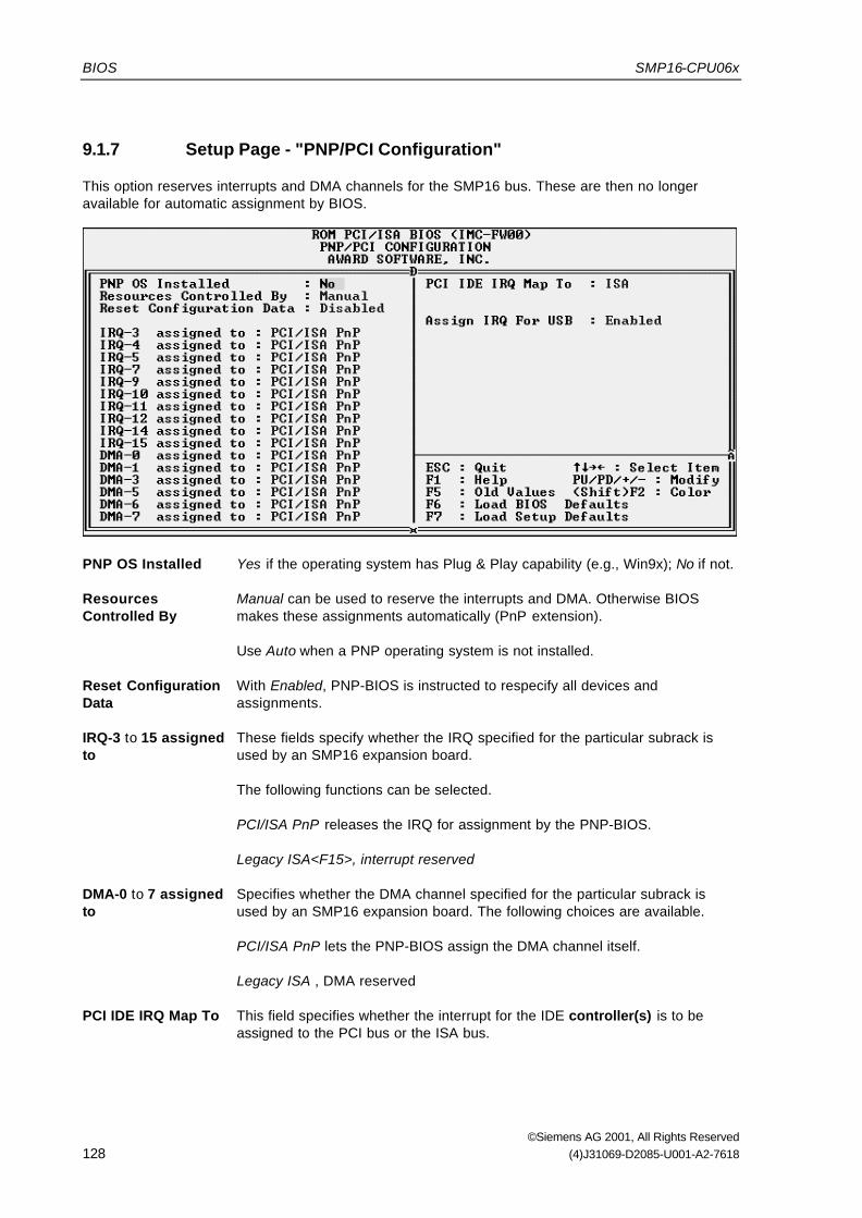
BIOS SMP16-CPU06x
©Siemens AG 2001, All Rights Reserved128 (4)J31069-D2085-U001-A2-7618
9.1.7 Setup Page - "PNP/PCI Configuration"
This option reserves interrupts and DMA channels for the SMP16 bus. These are then no longeravailable for automatic assignment by BIOS.
PNP OS Installed Yes if the operating system has Plug & Play capability (e.g., Win9x); No if not.
ResourcesControlled By
Manual can be used to reserve the interrupts and DMA. Otherwise BIOSmakes these assignments automatically (PnP extension).
Use Auto when a PNP operating system is not installed.
Reset ConfigurationData
With Enabled, PNP-BIOS is instructed to respecify all devices andassignments.
IRQ-3 to 15 assignedto
These fields specify whether the IRQ specified for the particular subrack isused by an SMP16 expansion board.
The following functions can be selected.
PCI/ISA PnP releases the IRQ for assignment by the PNP-BIOS.
Legacy ISA<F15>, interrupt reserved
DMA-0 to 7 assignedto
Specifies whether the DMA channel specified for the particular subrack isused by an SMP16 expansion board. The following choices are available.
PCI/ISA PnP lets the PNP-BIOS assign the DMA channel itself.
Legacy ISA , DMA reserved
PCI IDE IRQ Map To This field specifies whether the interrupt for the IDE controller(s) is to beassigned to the PCI bus or the ISA bus.

SMP16-CPU06x BIOS
©Siemens AG 2001, All Rights Reserved(4)J31069-D2085-U001-A2-7618 129
Primary IDE INT#/Secondary IDE INT#
Explicitly assigns a PCI IRQ for the primary and secondary IDE channel
Choices are: INTs A, B, C and D.
Assign IRQ for USB When Enabled, a PCI-IRQ is assigned to the USB controller.

BIOS SMP16-CPU06x
©Siemens AG 2001, All Rights Reserved130 (4)J31069-D2085-U001-A2-7618
9.1.8 Setup Page - "Load BIOS Defaults" and "Load Setup Defaults"
"Load Setup Defaults" lets you load the basic settings with which the board always functions. Incontrast, "Load BIOS Defaults" loads optimized presettings for normal operation. If you select thepresettings in this menu, all affected settings are changed.
When pages in the main menu are selected, the following dialog screen appears.
<Y> loads the presettings.
<RETURN> or <N> causes the message to disappear, and the presettings are not loaded.
Note:These menu items reset the settings of all Setup pages to their default values!
In addition to the two default settings, other settings can be made to increase board performance(e.g., cacheability, SDRAM parameters, and so on).If this causes problems, it is easy to return to a stable state again by using the default settings.

SMP16-CPU06x BIOS
©Siemens AG 2001, All Rights Reserved(4)J31069-D2085-U001-A2-7618 131
9.1.9 Setup Page - "Integrated Peripherals"
The settings of the peripherals are specified on this page.
PCI IDE 2nd Channel Can be used to enable an external secondary PCI-IDE controller (prerequisite:on-board secondary IDE controlled is disabled).
IDE HDD BlockMode
Can be used to have entire blocks transferred instead of single sectors fromhard disk to memory.
IDE 32-bit TransferMode
The integrated IDE interface supports 32-bit data transmission. Only enablethis option when the drive also supports this.
On-Chip PrimaryPCI IDE / On-ChipSecondary PCI IDE
When you activate this field, the modes in which the IDE devices can beoperated become variable.
The following choices are available. For PIO: Mode0 to 4 and Auto. ForUDMA: enable, disable and Auto. With Auto, the mode which the systemreads from hard disk is taken.
USB KeyboardSupport
When this option is enabled, a keyboard on the USB port is also supportedafter the boot procedure.
Init Display First This option can be used to specify which graphics card is to be used for videooutput when both an AGP and a PCI graphics card are integrated in thesystem. When a graphics card is connected to the SMP16 bus, this card isalways used for video output regardless of the setting.

BIOS SMP16-CPU06x
©Siemens AG 2001, All Rights Reserved132 (4)J31069-D2085-U001-A2-7618
Onboard LAN If Disabled, BIOS does not assign an interrupt to the on-board LAN controller.
Attention:An operating system with Plug&Play capability (e.g., Win9x) automaticallyrecognizes PCI devices and attempts to install the appropriate drivers.However, the device doesn't function due to the missing interrupt.
Note:With the SMP16-CPU066, the LAN controller is deactivated on the hardwareso that the above problem doesn't exist.
Onboard FDCController
Activation of the on-board floppy disk controller
Onboard Serial Port1
Sets the I/O addresses and IRQs of serial port 1 (COM A:)
3F8 / IRQ42F8 / IRQ33E8 / IRQ42E8 / IRQ3Disabled
Onboard Serial Port2
Sets the I/O addresses and IRQs of serial port 2 (COM B:)
3F8 / IRQ42F8 / IRQ33E8 / IRQ42E8 / IRQ3Disabled
Onboard ParallelPort
Sets the I/O addresses and IRQs of the parallel port
378 / IRQ7Disabled
Parallel Port Mode Sets the mode of the parallel port. This option appears when 378 / IRQ7 is setin Onboard Parallel Port.
The following choices are available.
ECP+EPP1.9ECPEPP1.9+SPPSPPECP+EPP1.7EPP1.7+SPPNormal
ECP Mode Use DMA This message appears when ECP+EPP1.9, ECP or ECP+EPP1.7 is selectedin <F0>Parallel Port Mode<F15>. The DMA channel is permanently set to 1and cannot be changed.

SMP16-CPU06x BIOS
©Siemens AG 2001, All Rights Reserved(4)J31069-D2085-U001-A2-7618 133
9.1.10 Setup Page - "IMC Miscellaneous"
Enable CTRL-C/CTRL-Break
When No is entered, this option causes the key combination <CTRL-C>/<CTRL-Break> to be intercepted by BIOS and not sent to the operatingsystem. Yes reactivates the keys. The user can also change this functionduring running operation. When software interrupt 16h is triggered by AH = 3,AL = 49h and BL = 0, <CTRL-C>/<CTRL-Break>is permitted. These key combinations are suppressed with BL= 1..
SMP16-Bus When this option is set to disabled, the SMP16 bus becomes high ohmic afterthe boot procedure. Cards on this bus cannot be accessed.
SMP16-Clocks This option switches off the 8.33 MHz and 14.131 MHz clock pulse of theSMP16 bus. This setting can only be made when the SMP16 bus is enabled.
Use of LED L1 Prim. HD: LED goes on when a primary hard disk is accessed.User: LED can be turned on/off by the user.
(see chapter 7.2.1.6, (bit 0 of I/O address 4034H)
Use of LED L2 Sec. HD: LED goes on when a primary hard disk is accessed.
User: LED can be turned on/off by the user.(see chapter , 7.2.1.6, (bit 0o f I/O address 4035H)
Use of LED L3 LAN: LED goes on when collision occurs on LAN.User: LED can be turned on/off by the user.
(see chapter 7.2.1.6, bit 3 of I/O address 4037H)
Use of LED L4 LAN: LED goes on when on-board LAN is sending.User: LED can be turned on/off by the user.
(see chapter , 7.2.1.6, bit 4 of I/O address 4037H)
IOCHCK-NMI This option specifies whether the NMI is enabled or disabled after the bootprocedure.

BIOS SMP16-CPU06x
©Siemens AG 2001, All Rights Reserved134 (4)J31069-D2085-U001-A2-7618
On board SRAM size Sets the size of an address window for the on-board SRAM. The followingsettings are available.
Disabled8kByte16kByte32kByte
Other settings can be made by the user's application (see chapter 7.2.1.13).
On board SRAMbase adr.
This value specifies the base address of the SRAM window. This value canonly be set when the SRAM is not disabled. Selection of the base addressdepends on the size of the window set.
Base Address Possible for SRAM Size in KbytesCC000H 8/16CE000H 8D0000H 8/16/32D2000H 8D4000H 8/16D6000H 8D8000H 8/16/32DA000H 8DC000H 8/16DE000H 8E0000H 8/16/32E2000H 8E4000H 8/16E6000H 8
Fanless Operation When this option is enabled, the board can be run without a fan. Theprocessor is then only in operation 50% of the time.
Attention:The Power Management functions in BIOS and the operating system must have been deactivatedsince these might overwrite the setting.

SMP16-CPU06x BIOS
©Siemens AG 2001, All Rights Reserved(4)J31069-D2085-U001-A2-7618 135
9.1.11 Setup Page - "Password Setting"
This option is used to set the Setup password. Activate this option when you want to specify apassword. A dialog screen appears in which you can specify the password. Remember that thecomputer distinguishes between upper case and lower case letters and the password may have up toeight alphanumeric characters. When a password has been entered, the password is requested whenthe Setup page is called.
Before password protection can be activated, it must be specified in the Security Option of the BIOSFEATURES SETUP menu when the system is to request the password.
To deactivate the password, press the <RETURN> key when the "Enter Password" dialog boxappears. A message then confirms that the password has been deactivated.
9.1.12 Setup Page - "IDE HDD Auto Detection"
This option determines the parameters of an IDE hard disk and enters them automatically inSTANDARD CMOS SETUP.
Up to four IDE drives can be detected. The parameters for each hard disk are shown in succession ina box.
The values are accepted by pressing the <Y> key or selecting one of the numbers in the OPTIONSfield (in our case 2, 1).
Press the <N> key to jump to the next hard disk.
The detected values are entered in the table in STANDARD CMOS SETUP as user values.
Note:Since the Elite BIOS of the SMP16-CPU06x calculates the hard disk parameters differently than thePower BIOS of the SMP16-CPU055 (particularly in LBA mode), the hard disk may have to bereformatted and a new installation performed.

BIOS SMP16-CPU06x
©Siemens AG 2001, All Rights Reserved136 (4)J31069-D2085-U001-A2-7618
9.1.13 Setup Page - "Save & Exit Setup"
This option is used to save all values entered during the current session to the CMOS memory. Afteryou select the Setup option, the following dialog screen appears.
Use <Y> to save and exit Setup.
Press <RETURN> or <N> and the message disappears.

SMP16-CPU06x BIOS
©Siemens AG 2001, All Rights Reserved(4)J31069-D2085-U001-A2-7618 137
9.1.14 Setup Page - "Exit Without Saving"
This option can be used to exit the Setup service program without saving. After activation, thefollowing message appears.
Use <Y> to exit Setup's main menu without saving.
Press <RETURN> and <N> and the message disappears.

BIOS SMP16-CPU06x
©Siemens AG 2001, All Rights Reserved138 (4)J31069-D2085-U001-A2-7618
9.1.15 Setup - Default Setting
Setup Page Parameter BIOS DefaultValues
Setup DefaultValues
Virus Warning Disabled
CPU Internal Cache Enabled
External Cache Enabled
CPU L2 Cache ECC Checking Enabled
Quick Power On Self Test Enabled Disabled
Boot From LAN First Disabled
Boot Sequence A, C, SCSI
Swap Floppy Drive Disabled
Boot Up Floppy Seek Disabled Enabled
Boot Up Numlock Status On
Gate A20 Option Fast
Typematic Rate Setting Disabled
Typematic Rate (Chars/Sec) (6)
Typematic Delay (Msec) (250)
Security Option Setup
PS/2 mouse function control Enabled
PCI/VGA Palette Snoop Disabled
Assign IRQ For VGA Disabled
OS Select For DRAM > 64MB Non-OS2
Report No FDD For WIN 95 No Yes
Video BIOS Shadow Enabled
C8000-CFFFF Shadow bis DC000-DFFF Disabled
Award Preboot Agent Disabled Enabled
Agent Host Drive A Disabled
Agent after boot Disabled
SDRAM RAS-to-CAS Delay 3
SDRAM RAS Precharge Time 3
SDRAM CAS latency Time 3/2 1)
SDRAM Precharge Control Disabled
DRAM Data Integrity Mode Non-ECC
System BIOS Cacheable Disabled
Video BIOS Cacheable Enabled Disabled
Video RAM Cacheable Disabled
8 Bit I/O Recovery Time 1
16 Bit I/O Recovery Time 1
Memory Hole At 15M-16M Disabled
Passive Release Enabled
Delayed Transaction Disabled
AGP Aperture Size (MB) 64
ACPI Disabled
Power Management User Defined
PM Control by APM Yes

SMP16-CPU06x BIOS
©Siemens AG 2001, All Rights Reserved(4)J31069-D2085-U001-A2-7618 139
Setup Page Parameter BIOS DefaultValues
Setup DefaultValues
Video Off Method V/H SYNC + Blank
Video Off After Standby
MODEM Use IRQ 3 NA
Doze Mode Disabled
Standby Mode Disabled
Suspend Mode Disabled
HDD Power Down Disabled
Throttle Duty Cycle 62.5%
Power Management Setup, PCI/VGA Act-Monitor Disabled
continued Power On by Ring Enabled Disabled
SpeedStep Support 2)
IRQ 8 Break Suspend Disabled
IRQ [3-7, 9-15], NMI Disabled
Primary IDE 0 Disabled
Primary IDE 1 Disabled
Secondary IDE 0 Disabled
Secondary IDE 1 Disabled
Floppy Disk Disabled
Serial Port Enabled
Parallel Port Disabled
PNP OS Installed No
Ressources Controlled By Auto Manual
Reset Configuration Data Disabled
IRQ-3 to 15 assigned to (PCI/ISA PnP) PCI/ISA PnP
DMA0, 1 to 7 assigned to (PCI/ISA PnP) PCI/ISA PnP
PCI IDE IRQ Map To ISA
Primary IDE INT (A)
Secondary IDE INT (B)
Assign IRQ For USB Enabled
PCI IDE 2nd Channel Enabled
IDE HDD Block Mode Disabled Enabled
IDE 32-bit Transfer Mode Disabled
On-Chip Primary PCI IDE Enabled
IDE Primary Master PIO Auto
IDE Primary Slave PIO Auto
IDE Primary Master UDMA Auto
Integrated Peripherals IDE Primary Slave UDMA Auto
On-Chip Secondary PCI IDE Enabled / Disabled 3)
IDE Secondary Master PIO Auto
IDE Secondary Slave PIO Auto
IDE Secondary Master UDMA Auto
IDE Secondary Slave UDMA Auto
USB Keyboard Support Enabled
Init Display First PCI Slot

BIOS SMP16-CPU06x
©Siemens AG 2001, All Rights Reserved140 (4)J31069-D2085-U001-A2-7618
Setup Page Parameter BIOS DefaultValues
Setup DefaultValues
Onboard LAN Enabled
Onboard FDC Controller Enabled / Disabled 3)
Integrated Peripherals, Onboard Serial Port 1 3F8/IRQ4
continued Onboard Serial Port 2 2F8/IRQ3
Onboard Parallel Port 378/IRQ7
Parallel Port Mode ECP + EPP1.9
ECP Mode Use DMA 1
Enable CTRL-C/CTRL-Break Yes
SMP16 bus Enabled
SMP16-Clock Enabled
Use of LED L1 primary HD
Use of LED L2 secondary HD
Use of LED L3 LAN
Use of LED L4 LAN
IOCHCK-NMI Disabled
Onboard SRAM size Disabled
Onboard SRAM Base Address (CC000H)
Fanless Operation Disabled 4)
1) Starting with BIOS version 2.08: CAS Latency set to 2
2) Future expansions. Shows the clock-pulse frequency of the mobile module. Prerequisite: a module withSpeedStep capability is installed. Otherwise menu item is not shown.
3) Enabled for SMP16-CPU065. Disabled for SMP16-CPU066.
4) For modules with Pentium III processors (starting at 500 MHz): This Setup option is no longer available(fanless operation not permitted!).

SMP16-CPU06x BIOS
©Siemens AG 2001, All Rights Reserved(4)J31069-D2085-U001-A2-7618 141
9.2 LAN Boot BIOS
The boot BIOS extension for the LAN boot is located in BIOS flash. When activated in Setup (seechapter 9.1.4), this is jumped to. The following message appears on the monitor screen.
Novell NetWare Ready Firmware v1.00 (940810)(C) Copyright 1991 - 1994 Novell, Inc. All Rights Reserved
Press <Home> key to boot from local Drive
After the above message appears, you have approx. 2 seconds to press the <Home> / <Pos1> key tobypass the LAN boot. A selection of servers for the LAN boot then appears.
Novell NetWare Ready Firmware v1.00 (940810)(C) Copyright 1991 - 1994 Novell, Inc. All Rights ReservedAMD PCNTNW Ethernet MLID v3.00 (950630)(C) Copyright 1991 - 1995 AMD, Inc. all rights Reserved
To boot from Novell Server, press 1To boot from IBM LAN Server 2.x/3.x, press 2To boot from IBM LAN Server 4.x, press 3To boot from Microsoft Lan Manager Server, press 4To boot from first available Server, press 5If no selection within 10 seconds, will use choice 5 Please, make your choice now!
If you don't make your choice now, BIOS attempts to boot from the first available servers. The LAN-boot BIOS makes 10 attempts to establish a connection. During this, the following is displayed on yourscreen.
RPL-ROM-ADR: 0800 06xx xxxx (Ethernet address of the board: 0800 06.. for Siemens)RPL-ROM-IRQ: 12 (Assigned interrupt; depends on system environ.)RPL-ROM-PIO: E400 (PCI-IO address; depends on system environ.)
RPL-ROM-FFC: 1 (Counts from 1 to 10)
When all attempts to boot fail, the set boot sequence is used (see chapter 9.1.4).

BIOS SMP16-CPU06x
©Siemens AG 2001, All Rights Reserved142 (4)J31069-D2085-U001-A2-7618
9.3 BIOS Flash Memory
The BIOS flash memory permanently installed on the board is divided into blocks of different sizes.These blocks can be cleared and rewritten with a BIOS update (see chapter 10). The following figureshows the physical arrangement of the block.
F C000 Minimal BIOS
ESCD
Microcode
16 kbytes
8 kbytes
8 kbytes
Main BIOS
96 kbytes
F A000
F 8000
F 0000
128 kbytes
E FFFF
D 0000C FFFF
F FFFF h
BIOS extensionand
system BIOS256 kbytes
786
kbyt
es
C 0000 h
USERDATA
B FFFF h
0 0000 h
CDT
Preboot Agent(if enabledafter boot)
E 0000
Figure 9.1 Organization of the BIOS flash memory

SMP16-CPU06x BIOS
©Siemens AG 2001, All Rights Reserved(4)J31069-D2085-U001-A2-7618 143
9.4 ROM-BIOS Interrupts
All ROM-BIOS interrupts are listed here.
Interrupt Meaning Source
INT 00h Division by 0 CPU
INT 01h Single step (trap) CPU
INT 02h NMI (with PCs and ATs, among others: parity error) CPU
INT 03h Breakpoint (INT command) CPU
INT 04h Arithmetic overflow (INT0 command) CPU
INT 05h Address of the routine which is jumped to when the Shift-PrtSc key combination ispressed (e.g., the loadable GRAPHICS program for a graphic hardcopy or, in textmode, a ROM-BIOS routine)
Software
INT 06h Invalid operation code CPU
INT 07h Coprocessor is not available. CPU
INT 08h Counter hardware interrupt (IRQ 0, system clock) Hardware
INT 09h Keyboard interrupt (IRQ 1, keyboard hardware). Transfers the scan code of apressed or released key on I/O port 60h. The interrupt routine supplements thiswith the appropriate ASCII character and writes it to the keyboard buffer.
Hardware
INT 0Ah IRQ 2; cascaded second interrupt controller Hardware
INT 0Bh COM_B interrupt Hardware
INT 0Ch COM_A interrupt Hardware
INT 0Dh LPT2 interrupt Software
INT 0Eh Disk controller Software
INT 0Fh LPT1 interrupt Software
INT 10h Monitor screen interrupt Software
INT 11h Hardware test Software
INT 12h Memory size; no input; output: AX = RAM size in 1-kbyte blocks as per CMOS-RAM (AT)
Software
INT 13h Floppy disk/hard disk interrupt Software
INT 14h V.24 interfaces Software
INT 15h Interrupts of special functions Software
INT 16h Keyboard interrupt Software
INT 17h Printer output Software
INT 18h Reserved Software
INT 19h BootstrapSector 0 on track 0 of drive A: or C: is loaded starting at address 0000 7C00, and ajump to there is made to load the operating system from floppy disk or hard disk.
Software
INT 1Ah System time Software
INT 1Bh CTRL break vectorThis is where the keyboard interrupt program (INT 09h) jumps when the keycombination CTRL-Break is pressed.
Software
INT 1Ch Counter interruptIs jumped to 18.3 times per second. User programs which reroute the vector shouldjump to the previous address at the end of the interrupt routine (daisy chain).
User
INT 1Dh Monitor screen parametersAddress of the parameter table for INT 10h/AH = 0
BIOS table
INT 1Eh Disk parametersAddress of the current disk parameter block
BIOS table

BIOS SMP16-CPU06x
©Siemens AG 2001, All Rights Reserved144 (4)J31069-D2085-U001-A2-7618
Interrupt Meaning Source
INT 1Fh Graphic fontStart address of the 8x8 graphic font (can be loaded with GRAFTABL) for theexpanded IBM font(Codes 128 to 255, CGA+EGA).
User
INT 20h toINT 3Fh
Reserved for DOS
INT 40h Floppy disk BIOS revector Software
INT 41h Parameter table of the hard disk BIOS table
INT 42h EGA default video driver BIOS table
INT 43h Video graphics character User
INT 44h toINT 45h
Reserved
INT 46h Parameter table of the hard disk BIOS table
INT 47h toINT 49h
Reserved
INT 4Ah User alarm User
INT 4Bh toINT 59h
Reserved
INT 5Ah Device adapter
INT 5Bh toINT 5Fh
Reserved
INT 60h toINT 66h
Reserved for interrupts of the user program User
INT 67h LIM EMS driver (only AT)
INT 68h toINT 6Fh
Reserved
INT 70h IRQ 8 (realtime clock) Hardware
INT 71h IRQ 9 Hardware
INT 72h IRQ 10 Hardware
INT 73h IRQ 11 Hardware
INT 74h IRQ 12 Hardware
INT 75h IRQ 13 (coprocessor) User
INT 76h IRQ 14 (hard disk controller) Hardware
INT 77h IRQ 15 Hardware
INT 78h toINT 7Fh
Reserved
INT 80h toINT F0h
Reserved for BASIC BASIC
INT F1h toINT FFh
Reserved for interrupts of the user program User

SMP16-CPU06x BIOS
©Siemens AG 2001, All Rights Reserved(4)J31069-D2085-U001-A2-7618 145
9.5 BIOS Data Area
The following table shows the assignment of the BIOS data area (BDA = BIOS Data Area) starting inthe DRAM at address 0040:0000h.
Address No. ofBytes
Contents
0000h 2 I/O address of COM1
0002 h 2 I/O address of COM2
0004 h 2 I/O address of COM3
0006 h 2 I/O address of COM4
0008 h 2 I/O address of LPT1
000Ah 2 I/O address of LPT2
000Ch 2 I/O-Adresse of LPT3Note: Unassigned interface vectors contain 0000.
000Eh 2 Segment address of BIOS data area
0010 h 2 Flags for external hardware
0012 h 1 INIT flag
0013 h 2 RAM size in kbytes
0015 h 2 INIT error flag
0017 h 3 Keyboard status (0017 = shift status)
001Ah 2 Keyboard buffer pointer 1
001Ch 2 Keyboard buffer pointer 2
001Eh 32 Keyboard buffer (16 words)
003Eh 11 Floppy disk controller status bytes
0049 h 1 Video display mode (see INT 10h, AH = 0!)
004Ah 2 Number of characters per line
004Ch 2 Size of the video RAM in bytes
004Eh 2 Address of the video RAM
0050 h 16 Cursor position (2 bytes per monitor screen page)
0060 h 2 Size of the cursor
0062 h 1 Number of the active display page
0063 h 2 Address of the video controller 6845
0065 h 1 Flag byte for video controller
0066 h 1 Colors for display
0067 h 4 Start address and segment of an extra ROM
006Bh 1 Flag for interrupt
006Ch 4 Counter-count for 8253 chip (system clock)
0070 h 1 Flag for next day after 24 hours
0071 h 1 Flag for CTRL-Break key (bit 7 = 1)
0072 h 2 Flag for triggering warm boot (value = 1234h: warm boot)
0074 h 4 Hard disk controller status bytes
0078 h 1 Timeout value for LPT1
0079 h 1 Timeout value for LPT2
007Ah 1 Timeout value for LPT3

BIOS SMP16-CPU06x
©Siemens AG 2001, All Rights Reserved146 (4)J31069-D2085-U001-A2-7618
Address No. ofBytes
Contents
007Bh 1 Reserved
007Ch 1 Timeout value for COM1
007Dh 1 Timeout value for COM2
007Eh 1 Timeout value for COM3
007Fh 1 Timeout value for COM4
0080 h 2 Start address of the keyboard buffer (= 001E)
0082 h 2 End address of the keyboard buffer (= 003E)
0084 h 7 Last line of the monitor screen page
008Bh 1 Transfer rate
008Ch 1 Status of the last hard disk operation
008Dh 1 Error in the last hard disk operation
008Eh 1 INT 76h mark for a hard disk interrupt
008Fh 1 Hard disk performance
0090 h 4 Media byte of the hard disk
0094 h 2 Current cylinder of the drives
0096 h 1
0097 h 1 Error of keyboard commands/last LED status
0098 h 4 Wait flag address
009Ch 4 Wait time before timeout
00A0h 1 Wait flag in use
00A1h 95 Reserved (do not change)
0100 h 1 1 = Screen hardcopy (PrtSc) running; 00FFh = error for PrtSc; otherwise 0

SMP16-CPU06x BIOS
©Siemens AG 2001, All Rights Reserved(4)J31069-D2085-U001-A2-7618 147

BIOS Update SMP16-CPU06x
©Siemens AG 2001, All Rights Reserved148 (4)J31069-D2085-U001-A2-7618
10 BIOS Update
10.1 System BIOS
Note:To update this BIOS you will need AWDFLASH.EXE, a program available from the Internet (seechapter Fehler! Verweisquelle konnte nicht gefunden werden.).
AWDFLASH.EXE
This is the service program with which you can load a new BIOS to the programmable flash chip of theboard. The BIOS version is indicated when the system starts up after the text string SMP16-CPU06x.The program can only be run under DOS. With Win95/98, "F8” must to pressed during system startupto access the DOS prompt.
10.2 The AWDFLASH.EXE Service Program
Warning
To program the screen on the SMP16-CPU06x, you will need the version ofAWDFLASH.EXE available on the Internet.If "unknown" appears after Flash Type, this ROM chip cannot be programmed withthis version of AWDFLASH.EXE.
Note:The call parameter /? gives you a list of possible command line parameters (only on systems withgraphics card, see chapter 10.3.2).

SMP16-CPU06x BIOS Update
©Siemens AG 2001, All Rights Reserved(4)J31069-D2085-U001-A2-7618 149
10.3 How To Update Your BIOS
10.3.1 System with Graphics Card
1. Download the new BIOS file from the Internet (WWW or FTP).
2. Start your computer in DOS mode.
3. Start the AWDFLASH.EXE program. During this you can also transfer the name of the new file ascall parameter. Example:
AWDFLASH File
If you don't enter a file name, the program will ask you to enter one.
4. You are now asked whether you want to make a backup of the existing BIOS. If you reply with Y,you will be asked to enter a name for the file under which you want to save your old BIOS.
5. You are now asked to confirm programming. If you reply with Y, the new BIOS is programmed toflash memory.
Attention:During programming, do not reset or turn off the system. The flash memory would be incompleteand the CPU would be unable to boot again.
6. After programming, you can start the system again by pressing the F1 key, and the modifiedBIOS takes effect. Pressing F10 gives you the DOS level but the old BIOS will still be used untilthe next system startup.
Note:The CMOS settings are retained for use when the updated BIOS starts up.
10.3.2 System with Console Rerouting without Graphics Card
Since the AWDFLASH.EXE program generates its monitor screen outputs without using INT10 (videointerrupt), you cannot see program messages on your terminal when console rerouting is used.However, you can specify all required entries when the program is called.
Enter the following to program a new BIOS and save the old version.
AWDFLASH <NEWBIOS> /Py <OLDBIOS> /Sy
Enter the following to program a new BIOS without saving the old version.
AWDFLASH <NEWBIOS> /Py /Sn
Note:After the last floppy disk access, wait approx. 1 minute, and then start the system again.

BSP-CPU06x: RMOS on the SMP16-CPU06x SMP16-CPU06x
©Siemens AG 2001, All Rights Reserved150 (4)J31069-D2085-U001-A2-7618
11 BSP-CPU06x: RMOS on the SMP16-CPU06xThe BSP-CPU06x includes an RMOS3-PC1 V3.20 configuration for the SMP16-CPU06x. Thedifferences from a standard PCI system are listed below.
• EIDE driver for secondary channel
• TCPIP connection for on-board LAN is integrated in the configuration.
• Support of the extra interrupt controller
• SRAM driver for buffered SRAM in memory hole (15 to 16 Mbytes)
In addition, there are functions for:
• Temperature monitoring
• Use of BIOS flash memory by the user
• Use of the serial EEPROM by the user
• Use of the buffered SRAM
• TEST6x.386 sample test program for checking the additional functions
All required expansions to the RMOS configuration are stored in the files RMCONF.C andRCCPU06x.C. Only the PC1 version is supported (not RMOS for Windows).
11.1 RMOS and Power Management/Fanless Operation
The BIOS of the SMP16-CPU06x makes it possible to activate different power management functions(see chapter 9.1.6) or fanless operation (see chapter 7.1.10).
When the RMOS operating system is loaded, the BIOS functions are replaced with RMOS functions.However, this does not apply to the power management functions (system management interrupt andhandler). These functions remain active.
Warning
When power management is active, an undesired transition to the power downsequence (doze, standby, suspend) can occur. Just as with "fanless operation"mode, realtime may not be guaranteed and, if activated, a watchdog may betriggered.

SMP16-CPU06x BSP-CPU06x: RMOS on the SMP16-CPU06x
©Siemens AG 2001, All Rights Reserved(4)J31069-D2085-U001-A2-7618 151
11.2 Installation Program
Proceed as follows to install the BSP-CPU06x on the developer's computer.
1. If not already done, install RMOS3 V3.20 on your development computer.
2. Place the floppy disk with the BSP-CPU06x in the floppy disk drive.
3. Start the installation program.A:\INSTALL.EXEThe installation program is controlled by the INI file PRODUCT.INI.
4. Follow the instructions of the program on your monitor screen.When you select RMOS3 as the destination system, the self-unpacking file PRODUCT3.EXE isunpacked under this destination directory.
The following overview shows the structure of the installed files.
(Destination directory) | READ_C6x.1Px Latest product information (this file) | +---LIB | | | +---CADUL | | R3CPU06x.LIB Library containing CPU06x driver (SRAM-Disk) | | driver-Configuration and CPU06x-Initializations. | | RM3UTL0.LIB Library containing the functions for accessing | | the ser. eeprom, feprom, temperature, ... | | PCIBX.LIB Library containing the functions for accessing | | the Intel BX-Chipset | | | \---BC | RM3UTL0B.LIB Library containing the functions for accessing | the ser. eeprom, feprom, temperature, ... | for Borland C++ V4.02/V4.5 | +---INC | RCCPU06x.SUB Subsystem for rccpu06x.c | RD40.H headerfile for the SRAM driver | UTIL0.H headerfile for the cpu06x specific functions | +---SYSTEM | | | \---PC_CPU6x | BOOTDISK.BAT Batch file to generate a boot disk | GENSYSC.BAT Batch file to generate RMOS for PC (CADUL) | GENSYSI.BAT Batch file to generate RMOS for PC (Intel) | GENTCPC.BAT Batch file to generate RMOS(TCPIP) for PC (CADUL) | GENTCPI.BAT Batch file to generate RMOS(TCPIP) for PC (Intel) | HW_PC1.ASM Startup code for PC - for use with CADUL and Intel | RCCPU06x.C Source of general CPU06x HW-Initializations | RCCPU06x.H Headerfile of general CPU06x HW-Initializations | RM3LPC1.BLD Builder input | RM3LTCP.BLD Builder input (with tcpip) | RMCONF.C Software configuration for PC | RMOS.INI RMOS configuration file | +---BIN | HDINIT.386 Loadable HD-initialization program | HDPART.386 Loadable HD-partitioning program +---EXAMPLES | | | \---HD | | HDINIT.C Main module for calling hd_init

BSP-CPU06x: RMOS on the SMP16-CPU06x SMP16-CPU06x
©Siemens AG 2001, All Rights Reserved152 (4)J31069-D2085-U001-A2-7618
| | | \---CPU6x | | TEST6x.C Loadable test-task, Source code | | | +---BC | | MAKEFILE Makefile to generate TEST6x.EXE | | TEST6x.EXE Loadable test-task | | | +---CADUL | | TEST6x.BAT Batch file to generate TEST6x.386 | | TEST6x.386 Loadable test-task | | | \---INTEL | TEST6x.BAT Batch file to generate TEST6x.386 | TEST6x.386 Loadable test-task | \---UTIL RFLASH.EXE flash loader (data area) for CPU06x
11.3 RMOS Configuration for the SMP16-CPU06x
The sample systems supplied with the BSP-CPU06x include the support of the secondary EIDEcontroller, the integration of the TCP/IP connection, the support of the additional interrupt controller,and the initialization of an SRAM driver in the memory hole.
The following sections explain the adjustments to the RMOS3 PC1 system which are required.
11.3.1 Support of the Secondary EIDE Controller
The BSP-CPU06x contains an extention for EIDE hard disks. This can also be used to address harddisks in LBA mode and to partition and format up to 8 Gbytes.
In addition, the BSP-CPU06x supports the secondary EIDE controller on the SMP16-CPU06x. Thispermits up to 3 hard disks to be used on the SMP16-CPU06x.
Note:After partitioning and formatting two hard disks (e.g., SMP16-MEM351 on the primary channel andIPCI-MEM361, or two hard disks via RPIO on the secondary channel) on the SMP16-CPU06x underMS-DOS, the sequence of the logical drive designators under RMOS3 is not the same as that underMS-DOS.
SMP16-MEM351 IPCI-MEM361 or PRIO hard diskOper. on primary IDE Oper. on secondary IDEController with 4 partitions Controller with 4 partitions
MS-DOS C:/E:/F:/G: D:/H:/I:/J:RMOS3 C:/D:/E:/F:/ G:/H:/I:/J:
In comparison to the product in RMOS3 V3.20, the following expansions have been introduced for theEIDE controller.
• The EIDE driver supports ATA-3.
• The EIDE driver supports LBA mode.
• The EIDE driver supports 32-bit data transfer.

SMP16-CPU06x BSP-CPU06x: RMOS on the SMP16-CPU06x
©Siemens AG 2001, All Rights Reserved(4)J31069-D2085-U001-A2-7618 153
• Hdinit.386 automatically determines the hard disk parameters and sets the default translationmode on the hard disk.
• Hdpart.386 supports 8-bit number entries for parameter "1st LBA" (required for large hard disks).
The following expansions were implemented in support of the secondary EIDE controller.
• The EIDE driver supports the addresses of the secondary channel.
• Hdinit.386 automatically recognizes the secondary channel. The BIOS parameters are onlyevaluated for the secondary channel when two hard disks were not detected on the primarychannel.
Note:The secondary channel only supports one hard disk. This means that a total of 3 hard disks (2hard disks on the primary channel and 1 hard disk on the secondary channel) can be used.
• During startup (RMCONF.C, RCCPU06x.C), a check is made to determine whether a hard disk isconnected to the secondary channel (check whether secondary IDE controller was enabled inBIOS – read hard disk register 0x376 - then write-access the hard disk). If yes, a driver with theaddresses for the secondary channel is installed, and the entry "SEC_CHANNEL" is made in thecatalog of resources. Handling of the secondary channel is entered with the compiler switch#define CPU06x (see RMCONF.C) in RMCONF.C and RCCPU06x.C (see below).
• Hdpart.386 supports the secondary channel.
Excerpt from the example RMCONF.C
#ifdef HSFS /* ---------------------------- */ /* Announce hard disks for HSFS */ /* ---------------------------- */ RcGetHardDiskType( &hdtype ); /* check if harddisk installed */ if ( hdtype & PCHD0 ) /* yes: announce hard disk 0 if present */ /* check free heapsize and use 10% of it for x_hd_init or 128KB */ err = RmGetMemPoolInfo(RM_HEAP, &mem); /* get free memory info */ if ( err ) freeheap = 0x20000ul; else freeheap = (0x200000ul < mem.avail_mem_size ? mem.avail_mem_size : 0x200000ul) / 10;
x_hd_init( Dev, /* Console device */ Unit, /* Console unit */ -1, /* Hardisk device (-1 = look for hd0) */ 0, /* Harddisk unit */ -1, /* Poolid (use heap) */ (long) freeheap, /* Max bytes of pool */ (uchar) 1, /* Interactive Mode; 1 == yes, 0 == no */ "C" /* Volume name to start from */ );#ifdef CPU06x SecUnit++;#endif
if ( hdtype & PCHD1 ) /* yes: announce hard disk 1 if present */

BSP-CPU06x: RMOS on the SMP16-CPU06x SMP16-CPU06x
©Siemens AG 2001, All Rights Reserved154 (4)J31069-D2085-U001-A2-7618
/* check free heapsize and use 10% of it for x_hd_init or 128KB */ err = RmGetMemPoolInfo(RM_HEAP, &mem); /* get free memory info */ if ( err ) freeheap = 0x20000ul; else freeheap = (0x200000ul < mem.avail_mem_size ? mem.avail_mem_size : 0x200000ul) / 10;
RmGetEntry(RM_CONTINUE, HD0DRV, &cat); /* search HD0 device */ x_hd_init( Dev, /* Console device */ Unit, /* Console unit */ (int) cat.id, /* Hardisk device (-1 = look for hd0) */ 1, /* Harddisk unit */ -1, /* Poolid (use heap) */ (long) freeheap, /* Max bytes of pool */ (uchar) 1, /* Interactive Mode; 1 == yes, 0 == no */ "D" /* Volume name to start from */ );#ifdef CPU06x SecUnit++;#endif #ifdef CPU06x if (inbyte(0x376) != 0xff) /* secondary channel */ dummy_in = inbyte(0x172); /* SecCount */ outbyte (0x172,0x5a); /* Test Pattern */ RmPauseTask(1); /* Recovery Time */ if (inbyte (0x172)==0x5a) char (* const Driven []) = "C", "D", "E"; outbyte( 0x172 , dummy_in); /* check free heapsize and use 10% of it for x_hd_init or 128KB */ err = RmGetMemPoolInfo(RM_HEAP, &mem); /* get free memory info */ if ( err ) freeheap = 0x20000ul; else freeheap = (0x200000ul < mem.avail_mem_size ? mem.avail_mem_size : 0x200000ul) / 10;
RmCatalog(RM_CATALOG_UNIT,SecUnit,0x00,"SEC_CHANNEL"); RmGetEntry(RM_CONTINUE, HD0DRV, &cat); /* search HD0 device */ x_hd_init( Dev, /* Console device */ Unit, /* Console unit */ (int) cat.id, /* Hardisk device (-1 = look for hd0) */ (int) SecUnit, /* Harddisk unit */ -1, /* Poolid (use heap) */ (long) freeheap, /* Max bytes of pool */ (uchar) 1, /* Interactive Mode; 1 == yes, 0 == no */ Driven[SecUnit] /* Volume name to start from */ ); #endif printf("\n");

SMP16-CPU06x BSP-CPU06x: RMOS on the SMP16-CPU06x
©Siemens AG 2001, All Rights Reserved(4)J31069-D2085-U001-A2-7618 155
Excerpt from the example RCCPU06x.C
/* function: RcInitHd0;; installs hd0 driver to RMOS;; return: errorcode*/int _FIXED _NEARRcInitHd0( void ) uint hdtype; int err; uint devno; uint SecUnit=0;
x_nucprintf(NUCMSG"init hd0 driver\n\r"); RcGetHardDiskType(&hdtype); /* get number and type of */ /* installed harddisks */#ifndef CPU06x if ( ! hdtype) x_nucprintf(NUCMSG"no harddisk found\n\r"); return RM_OK; /* no harddisk -> nothing to do */ #endif
err = RmCreateDriver( 0, HD0DRV, /* device name */ (RmDCDStruct *) &dcd, /* pointer to dcd */ &devno); if ( err ) return err;
if ( hdtype & PCHD0 ) /* harddisk 0 */ err = RcInitHd0Unit(0u, 0u); /* initialize unit 0 */ if ( err ) return err; SecUnit++; if ( hdtype & PCHD1 ) /* harddisk 1 */ err = RcInitHd0Unit(1u, 0u); /* initialize unit 1 */ if ( err ) return err; SecUnit++; #ifdef CPU06x if (inbyte(0x376) != 0xff) /* secondary channel */ err = RcInitHd0Unit(SecUnit, 1u); /* initialize sec. unit */ if ( err ) return err; #endif return RM_OK ;
/* function: RcInitHd0Unit;;; return: errorcode*/static int _FIXED _NEARRcInitHd0Unit( uint drive, uint secondary ) UCD_HD0 ucd;

BSP-CPU06x: RMOS on the SMP16-CPU06x SMP16-CPU06x
©Siemens AG 2001, All Rights Reserved156 (4)J31069-D2085-U001-A2-7618
char unitname[32]; int err; uint unitno;
if ( secondary ) x_nucprintf(NUCMSG"harddisk second channel %d\n\r",drive); else x_nucprintf(NUCMSG"harddisk primary channel %d\n\r",drive); ucd = ucd_init; if ( (drive == 1) && (!secondary) ) ucd.spec.type_mode |= 0x10; /* set second HD drive */ sprintf(unitname,HD0UNIT "%c",'0'+drive); if ( secondary ) ucd.spec.disk_req = 0x376; /* second channel */ ucd.spec.base_hdc = 0x170; /* second channel */
err = RmCreateUnit( HD0DRV, /* device name */ unitname, /* unit name */ (RmUCDStruct *) &ucd, /* pointer to ucd */ &unitno); if ( err ) return err;
/* set interrupt handler */ /* for harddisk drive */ if ( secondary ) err = RmSetDeviceHandler(IRQ15, /* IRQ */ HD0DRV, /* device name */ unitname, /* unit name */ X_HD0_INTR); /* interrupt entry point */ else err = RmSetDeviceHandler(IRQ14, /* IRQ */ HD0DRV, /* device name */ unitname, /* unit name */ X_HD0_INTR); /* interrupt entry point */ return err;

SMP16-CPU06x BSP-CPU06x: RMOS on the SMP16-CPU06x
©Siemens AG 2001, All Rights Reserved(4)J31069-D2085-U001-A2-7618 157
11.3.2 TCP/IP Connection
The RMOS configuration contains the configuration for the TCP/IP connection for the on-board LANchip of the CPU board. The stack and the driver are loaded dynamically at runtime (RMOS.INI). Staticconfiguration is also possible by removing the NO_COM291 switch in RMCONF.C.
Required accessories
The RMOS3-TCP/IP package must be ordered separately.
The PCILAN.DRV driver for the on-board LAN block is included in the BSP-TCPDRIV package. TheBSP-TCPDRV is available on the Internet under the following address.
• http://www.ad.siemens.de/sicomp/index.shtml(SICOMP-Homepage).
• Support
• FAQ's, Tipps & Tricks, Infos, Downloads, Dokumentation
• SICOMP Industrierechner > SICOMP SMP > Software für SMP > Baugruppensoftware
• Downloads
Attention:PCI group interrupts may not be used (i.e., when there are 2 PCI boards, 2 different interrupts mustalso be set in BIOS). See chapter 7.1.7.
Two generation batches (GENTCPC.BAT and GENTCPI.BAT) are included for linking the dynamicTCP/IP driver to the RMOS3-PC1 system. A bootable RMOS3-PC1 system can be generated after thesystem has been compiled and the "REM" commentary characters have been removed from theRMOS.INI file.
Note:The BSP-CPU06x only contains batch files GENTCPC.BAT and GENTCPI.BAT for generation of thedynamic TCP/IP connection. The TCP/IP connection cannot be used without the RMOS3-TCPIPpackage (stack, utilities) and the drivers in BSP-TCPDRIV.
The following excerpt shows the modifications required in the RMOS.INI file.
Excerpt from sample RMOS.INI[RMOS] rate=1ms logsvcx=YES sysdev=BYT_EGA_0
run=A:\BIN\LOADER.386 A:\BIN\PCILAN.DRVrun=A:\BIN\LOADER.386 A:\BIN\TCPIP.DRVrun=A:\BIN\TCPCONF.386 ETH970_MBX 0 130.205.32.199 255.255.0.0

BSP-CPU06x: RMOS on the SMP16-CPU06x SMP16-CPU06x
©Siemens AG 2001, All Rights Reserved158 (4)J31069-D2085-U001-A2-7618
11.3.3 Extra Interrupt Controller
The third 82C59 interrupt controller (see chapter 7.2.1.1, will now be referred to as the PCSSPIC - PCSoft Slave Programmable Interrupt Controller) is supported with the aid of the BSP-COM224.
• Addition of the SSPIC handler X_INT_SSPIC to the file HW_PC1.ASM
• Implementation of the procedures RcSetPICMaskPC(), RcInitSSPIC() and RcEOIProcPC() in thefile RCCPU06x.C
• Provision of predefined variables in RCCPU06x.H.
• Adjustment of the RMCONF.C file
IRQ5 (SSPIC_IRQ5) or IRQ9 (SSPIC_IRQ9) interrupts are provided for the cascading of the thirdinterrupt controller (see RCCPU06x.H).
IRQ5 is used as the default interrupt for the PCSSPIC. Using the interrupt matrix for the additionalinterrupt (control register 1, address 0x178 (bit 0 – bit 2), see 5.2.1.7), the output of the PCSSPIC isconnected to an interrupt input of the master interrupt controller (PCMPIC, IRQ5) or slave interruptcontroller (PCSPIC, IRQ9).
Attention:After the third interrupt controller is integrated, the default interrupt (e.g., IRQ5, SMP16 bus: c19 orPCI interrupt) can no longer be used as desired.If integration of the third interrupt controller is to be suppressed, #define SSPIC_IRQ5 must beremoved from RCCPU06x.H.
Excerpt from example RCCPU06x.H/* none or one define "SSPIC_IRQxx" is allowed to use */#define SSPIC_IRQ5 /* IRQ5 is used for 3. pic */
#define SSPIC_VECTOR_BASE 0x80 /* vector base 3.PIC */#define SSPIC_IRQ_MASK 0xFF /* mask 3.PIC */#define PCSSPIC_BASE 0x130 /* base address 3. PIC */#define PCSSPIC_MASK PCSSPIC_BASE + 1 /* mask 3. PIC */
#ifdef SSPIC_IRQ5#define IRQ_INT IRQ5#define IRQ_MASK0 0x01fu#define IRQ_MASK1 0x020u#define IRQ_NAME "IRQ5"#endif /* end '#if SSPIC_IRQ5' */
#ifdef SSPIC_IRQ9#define IRQ_INT IRQ9#define IRQ_MASK0 0x001u#define IRQ_MASK1 0x002u#define IRQ_NAME "IRQ9"#endif /* end '#if SSPIC_IRQ9' */

SMP16-CPU06x BSP-CPU06x: RMOS on the SMP16-CPU06x
©Siemens AG 2001, All Rights Reserved(4)J31069-D2085-U001-A2-7618 159
11.3.4 SRAM Driver
The buffered 128-kbyte SRAM (see chapter 4.2.4) is supported with the SRAM driver for the SMP16-CPU040 (RD40 driver of the BSP-CPU040). The driver emulates an SRAM disk. It is registered withthe RMOS file system so that the SRAM is used as a logical drive (drive R0:). If not already formatted,the driver automatically formats the SRAM disk during startup.
The SRAM driver is integrated in configuration file RMCONF.C with the switch #defineSRAM_DRIVER. The SRAM driver is configured (CPU control registers 17Ah and 17Dh, see chapters7.2.1.9 and 7.2.1.12) so that 128 kbytes of the memory hole can be utilized starting at base address0x0f80000. The following message appears during RMOS startup if the memory hole is not enabled.
NUC: Memory Hole disabled in Bios SetupNUC: SRAM-Driver not loaded
Note:The memory hole must be enabled in the BIOS of the CPU (see chapter 9.1.5) so that the SRAMdriver can be initialized.
When one or more SMP16-COM201s are used, make sure that the memory areas do not overlap.
11.3.4.1 Initialization Functions for the SRAM Driver
Configuration file RCCPU06x.C contains, among others, a default driver configuration (DCD and UCD)and functions for configuring and initializing the SRAM driver for the SMP16-CPU06x.
• DCD
• UCD for 1 unit
• RcInitSRAM(): Call in RMOS configuration portion
• RcInitSRAMenv(): Call in RMOS initialization task
The initialization data and functions are packed in accordance with the RMOS convention in aninitialization file in which the RcInitSRAM() function handles the entire driver initialization. In addition,the RcInitSRAMenv() function handles the registration of the driver with HSFS.
11.3.4.1.1 Constant Definitions for SRAM Driver
The constants required for initialization of the SRAM disk are defined in the RCCPU06x.H file.
#define RD40_RAM_ADR 0x0f80000l /* Start-address of SRAM-Disk (16MB)*/#define RD40_RAM_SIZE 128 /* Size in Kbytes of SRAM-Disk*/ /* (64 or 128) */#define RD40_SRB_BORDER 0x0 /* SRB limit */#define RD40_SRB_TIME 0x0 /* SRB delay time */

BSP-CPU06x: RMOS on the SMP16-CPU06x SMP16-CPU06x
©Siemens AG 2001, All Rights Reserved160 (4)J31069-D2085-U001-A2-7618
Note:The RD40_RAM_SIZE parameter may have to be adjusted to the actual SRAM size.
If you change parameters RD40_RAM_ADR and RD40_RAM_SIZE, you will also have to adjust theRcInitSRAM() initialization function in RCCPU06x.C.
11.3.4.1.2 RcInitSRAM Initialization Function
Function Generates operating system resources for SRAM driver
Include file <rccpu06x.h>
Syntax int RcInitSRAM(void)
Description The function performs the following steps.
• Generates the driver
• Generates the units of the driver
The function must be called during RMOS startup.
Return value 0 Conclusion successfulOther RMOS SVC error
This function must be called before the startup of RMOS.
Excerpt from the example RMCONF.C
x_nucprintf(NUCMSG"init 3964 com2: (SLAVE)\r\n"); /* init 3964 com2 unit */ ChkError( RcInit3964rCOM2( 19200ul, /* Baudrate */ DATA_8 | STOP_1 | NOPARITY, /* Mode */ 2, /* COM2 = SLAVE */ 0, /* Timeout Acknowledge */ 0 ) /* Timeout Character */ );#endif
/* new for CPU06x */#ifdef SRAM-DRIVER x_nucprintf(NUCMSG"config SRAM-driver\r\n"); /* init SRRAM-driver */ ChkError(RcInitSRAM());#endif /* SRAM_DRIVER */
x_nucprintf(NUCMSG"set system parameter\r\n");/*set console for output */ /*defined with SYS_CONSOLE */ ChkError( RmSetOS(ROUND_ROBIN,SVC_EXCEPTION_MESSAGE, syscon) );
#ifndef NO_REPORTER x_nucprintf(NUCMSG"create reporter\r\n"); ChkError( RcInitReporter(SYSTEMCONSOLE, /* system console */

SMP16-CPU06x BSP-CPU06x: RMOS on the SMP16-CPU06x
©Siemens AG 2001, All Rights Reserved(4)J31069-D2085-U001-A2-7618 161
11.3.4.1.3 RcInitSRAMenv Initialization Function
Function Initializes the driver environment
Include file <rccpu06x.h>
Syntax int RcInitSRAMenv (void)
Description Calls initialization function for HSFS (x_rd40_init())
When an error is detected, an error message is sent to the system console(see below). In addition, the messages of the x_rd40_init() function areoutput.
Return value 0 Conclusion successful-1 Error occurred
Error messages returned by x_rd40_init()
**** ERROR: RD40_INI: Cannot allocate memory !!!
**** ERROR: RD40_INI: HSFS: Creation of volume not successful !!!
**** ERROR: RD40_INI: Driver not installed !!!
**** ERROR: RD40_INI: HSFS: Error get volume status !!!
**** ERROR: RD40_INI: VIB already exists !!!
**** ERROR: RD40_INI: RmIO-Functioncall failed !!!
**** ERROR: RD40_INI: General device error !!!
**** ERROR: RD40_INI: Wrong number of units !!!
**** ERROR: RD40_INI: Unable to format Disk !!!
**** ERROR: RD40_INI: Parameter error !!!
**** ERROR: RD40_INI: Unexpected errorcode !!!
This function must be called in the Init task.
Excerpt from the example RMCONF.C
/* new for CPU06x */#ifdef SRAM_DRIVER RcInitSRAMenv(); /* Initialize HSFS and driver-environment */ /* for SRAM-driver for CPU06x. */#endif /* SRAM_DRIVER */
#ifndef NO_CLI /* -------------- */ /* Initialize CLI */ /* -------------- */ Status = RcInitCli();#endif

BSP-CPU06x: RMOS on the SMP16-CPU06x SMP16-CPU06x
©Siemens AG 2001, All Rights Reserved162 (4)J31069-D2085-U001-A2-7618
11.3.5 System Generation
Table 11.1 The library files required for system generation
RMOS Compiler Libraries Batch Files
RMOS3 CADUL R3CPU06x.LIB 1)
PCIBX.LIB 2)GENSYSC.BATGENTCPC.BAT
INTEL R3CPU06x.LIB 1)
PCIBX.LIB 2)GENSYSI.BATGENTCPI.BAT
1) Library contains drivers and configuration files for the SMP16-CPU06x2) Library contains system functions.
Batch file GENSYSC.BAT or GENSYSI.BAT creates an RMOS3-PCI system (without TCP/IP support).
Excerpt from the example GENSYSC.BAT
REM Compile the startup moduleAS386 HW_PC1.ASM -VSYMUPPER -DRM3=1@IF ERRORLEVEL 1 GOTO END:REM Compile the configuration and initialization module@ECHO OFFECHO -VANSI -VNEARFAR -VFIXEDPARAMS -VSYMUPPER > CC.CMDECHO -VFARCRT -D_ARCHITECTURE_=386 -DRM3=1 >>CC.CMDECHO -VNDP >>CC.CMDIF "%EMU%"=="TRUE" ECHO -DFPU_EMULATOR=1 >>CC.CMDECHO ONCC386 RMCONF.C -I%RBASE%\INC -VCOMPACT -VSUBSYS=RM3CFG.SUB -VROM -DNO_SOCKET2 -DNO_VC @CC.CMD@IF ERRORLEVEL 1 GOTO END:CC386 RCCPU06x.C -I%RBASE%\INC -VCOMPACT -VSUBSYS=RCCPU06x.SUB -VROM -VNOALIGN @CC.CMD@IF ERRORLEVEL 1 GOTO END:REM Link and locate the lot@ECHO OFFECHO HW_PC1.OBJ > BND_APL.CMDECHO RMCONF.OBJ >>BND_APL.CMDECHO RCCPU06x.OBJ >>BND_APL.CMDECHO %RBASE%\LIB\CADUL\RM3201.LIB >>BND_APL.CMDREM ECHO %RBASE%\LIB\CADUL\RM3201X.LIB >>BND_APL.CMDECHO %RBASE%\LIB\CADUL\RM3CFG.LIB >>BND_APL.CMDECHO %RBASE%\LIB\CADUL\PCIBX.LIB >>BND_APL.CMDECHO %RBASE%\LIB\CADUL\R3CPU06x.LIB >>BND_APL.CMDECHO %RBASE%\LIB\CADUL\RM3PC1.LIB >>BND_APL.CMDECHO %RBASE%\LIB\CADUL\RM3CF87C.LIB >>BND_APL.CMDECHO %RBASE%\LIB\CADUL\RM3BAS.LIB >>BND_APL.CMDIF "%EMU%"=="TRUE" ECHO %RBASE%\LIB\CADUL\E80387 >>BND_APL.CMDIF "%EMU%"=="TRUE" ECHO %RBASE%\LIB\CADUL\E80387.LIB >>BND_APL.CMDECHO %RBASE%\LIB\CADUL\80387FC.LIB >>BND_APL.CMDECHO -NAME RMOS3_V320_PC_IMAGE >>BND_APL.CMDECHO -SEGSIZE STACK=0 >>BND_APL.CMDECHO -SYMUPPER >>BND_APL.CMDECHO -INTELBIND >>BND_APL.CMDECHO ON:
REM Warning #383 can be ignored

SMP16-CPU06x BSP-CPU06x: RMOS on the SMP16-CPU06x
©Siemens AG 2001, All Rights Reserved(4)J31069-D2085-U001-A2-7618 163
:LINK386 -CF BND_APL.CMD -OJ RM3_PC1.LOC -PR RM3_PC1.MAP -BF RM3LPC1.BLD -TD .:%RBASE%\UTIL\QCOFTS RM3_PC1.LOC P386 L08000 UCOM:RMOS3_V320_PC_IMAGEGOTO END
Batch file GENTCPC.BAT or GENTCPI.BAT creates an RMOS3-PCI system with dynamic TCP/IPdrivers.
Excerpt from the example GENTCPC.BAT:
set TCP_LOAD=TRUE::ECHO ON:REM Compile the startup moduleAS386 HW_PC1.ASM -VSYMUPPER -DRM3=1@IF ERRORLEVEL 1 GOTO END:REM Compile the configuration and initialization module@ECHO OFFECHO -VANSI -VNEARFAR -VFIXEDPARAMS -VSYMUPPER > CC.CMDECHO -VFARCRT -D_ARCHITECTURE_=386 -DRM3=1 >>CC.CMDECHO -VNDP -VROM -I%PBASE%\INC -I%RBASE%\INC -IINCTCP >>CC.CMDECHO -VCOMPACT -L >>CC.CMDIF "%EMU%"=="TRUE" ECHO -DFPU_EMULATOR=1 >>CC.CMDECHO ONCC386 RMCONF.C -VSUBSYS=RM3CFG.SUB @CC.CMD@IF ERRORLEVEL 1 GOTO END:CC386 RCCPU06x.C -I%RBASE%\INC -VCOMPACT -VSUBSYS=RCCPU06x.SUB -VROM -VNOALIGN @CC.CMD@IF ERRORLEVEL 1 GOTO END:REM Link and locate the lot@ECHO OFFECHO HW_PC1.OBJ > BND_APL.CMDECHO RMCONF.OBJ >>BND_APL.CMDECHO RCCPU06x.OBJ >>BND_APL.CMDREM ECHO %RBASE%\LIB\CADUL\RM3201.LIB >>BND_APL.CMDREM ECHO %RBASE%\LIB\CADUL\RM3201X.LIB >>BND_APL.CMDECHO %RBASE%\LIB\CADUL\RM3CFG.LIB >>BND_APL.CMDIF "%TCP_LOAD%"=="TRUE" ECHO %PBASE%\LIB\CADUL\RMNOSOCK.LIB>>BND_APL.CMDIF "%TCP_LOAD%"=="FALSE" ECHO %PBASE%\LIB\CADUL\RMSOCKET.LIB >>BND_APL.CMDIF "%TCP_LOAD%"=="FALSE" ECHO %PBASE%\LIB\CADUL\RM3TCPIP.LIB >>BND_APL.CMDECHO %PBASE%\LIB\CADUL\RM3CRSK.LIB >>BND_APL.CMDECHO %PBASE%\LIB\CADUL\RM3SK2IF.LIB >>BND_APL.CMDECHO %PBASE%\LIB\CADUL\RM3SKXIF.LIB >>BND_APL.CMDECHO %RBASE%\LIB\CADUL\R3CPU06x.LIB >>BND_APL.CMDECHO %RBASE%\LIB\CADUL\PCIBX.LIB >>BND_APL.CMDECHO %RBASE%\LIB\CADUL\RM3PC1.LIB >>BND_APL.CMDECHO %RBASE%\LIB\CADUL\RM3CF87C.LIB >>BND_APL.CMDECHO %RBASE%\LIB\CADUL\RM3BAS.LIB >>BND_APL.CMDECHO %PBASE%\LIB\CADUL\R3ETH961.LIB >>BND_APL.CMDIF "%EMU%"=="TRUE" ECHO %RBASE%\LIB\CADUL\E80387 >>BND_APL.CMDIF "%EMU%"=="TRUE" ECHO %RBASE%\LIB\CADUL\E80387.LIB >>BND_APL.CMD

BSP-CPU06x: RMOS on the SMP16-CPU06x SMP16-CPU06x
©Siemens AG 2001, All Rights Reserved164 (4)J31069-D2085-U001-A2-7618
ECHO %RBASE%\LIB\CADUL\80387FC.LIB >>BND_APL.CMDECHO -NAME RMOS3_V320_PC_IMAGE >>BND_APL.CMDECHO -SEGSIZE STACK=0 >>BND_APL.CMDECHO -SYMUPPER >>BND_APL.CMDECHO -INTELBIND >>BND_APL.CMDECHO ON:REM Warning #383 can be ignored:LINK386 -CF BND_APL.CMD -OJ RM3_PC1.LOC -PR RM3_PC1.MAP -BF RM3LTCP.BLD -DB -TD . -SYMAP ALL:%RBASE%\UTIL\QCOFTS RM3_PC1.LOC P386 L08000 UCOM:RMOS3_V320_PC_IMAGEGOTO END:
Directory SYSTEM\PC_CPU6x contains a sample configuration for an RMOS-PC1 system.
File RMCONF.C contains the expansions for the SMP16-CPU06x.
These expansions are activated by the following instruction.
#define CPU06x /* activates the Initializations needed for CPU06x */
SMP16-CPU06x BSP-CPU06x: RMOS on the SMP16-CPU06x
©Siemens AG 2001, All Rights Reserved(4)J31069-D2085-U001-A2-7618 165
11.4 Additional Functions
Additional functions are included with the BSP-CPU06x which permit the user to use the new featuresof the SMP16-CPU06x.
• Temperature monitoring RcReadTemperatureCore()
• Use of the BIOS flash memory FEPROMRead(),
FEPROMWrite(),
FEPROMSecErase()
• Use of the serial EEPROM RcReadSerEEPROM(),
RCWriteSerEEPROM(),
RcGetMaxLengthSerEEPROM()
• Use of the buffered SRAM With RmIO system call
• TEST6x.386 sample test program forchecking the additional functions
TEST6x.386
11.4.1 Temperature Monitoring
The Pentium II mobile module is equipped with two temperature sensors (CORE and BX) which canbe read by the system management bus (SMB). These sensors generate an alarm when adjustablelimit values are exceeded.
BIOS specifies the limits for the CORE and BX temperature at 100° C each. If this limit is reached, so-called "throttling" is turned on. The throttling rate is permanently set by BIOS to 50%. (i.e., the CPU isonly on 50% of the time). When fanless operation is enabled in BIOS, the throttling rate is always 50%.This ensures operation within the module specifications even at an ambient temperature of55° C and fanless operation (or failure of the fan).
Attention:When throttling is activated, the realtime is no longer guaranteed, and a watchdog may be triggered.
Only the CORE temperature (processor temperature) is read. The temperature range is –127 degreesto +127 degrees. A temperature of more than 127 degrees is shown as 127 degrees. The temperatureis rounded off to the next whole number (e.g., 0.25 -> 0, 0.50 -> 1).
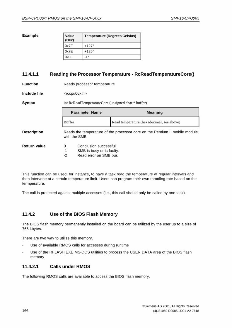
BSP-CPU06x: RMOS on the SMP16-CPU06x SMP16-CPU06x
©Siemens AG 2001, All Rights Reserved166 (4)J31069-D2085-U001-A2-7618
Example Value(Hex)
Temperature (Degrees Celsius)
0x7F +127°
0x7E +126°
0xFF -1°
11.4.1.1 Reading the Processor Temperature - RcReadTemperatureCore()
Function Reads processor temperature
Include file <rccpu06x.h>
Syntax int RcReadTemperatureCore (unsigned char * buffer)
Parameter Name Meaning
Buffer Read temperature (hexadecimal, see above)
Description Reads the temperature of the processor core on the Pentium II mobile modulewith the SMB
Return value 0 Conclusion successful-1 SMB is busy or is faulty.-2 Read error on SMB bus
This function can be used, for instance, to have a task read the temperature at regular intervals andthen intervene at a certain temperature limit. Users can program their own throttling rate based on thetermperature.
The call is protected against multiple accesses (i.e., this call should only be called by one task).
11.4.2 Use of the BIOS Flash Memory
The BIOS flash memory permanently installed on the board can be utilized by the user up to a size of766 kbytes.
There are two way to utilize this memory.
• Use of available RMOS calls for accesses during runtime
• Use of the RFLASH.EXE MS-DOS utilities to process the USER DATA area of the BIOS flashmemory
11.4.2.1 Calls under RMOS
The following RMOS calls are available to access the BIOS flash memory.

SMP16-CPU06x BSP-CPU06x: RMOS on the SMP16-CPU06x
©Siemens AG 2001, All Rights Reserved(4)J31069-D2085-U001-A2-7618 167
11.4.2.1.1 Reads USER AREA of the BIOS Flash - FEPROMRead
Function Read USER AREA of the BIOS flash
Include file <rccpu06x.h>
Syntax int FEPROMRead (unsigned int FEPROMAdrOffset,unsigned int Length,unsigned char * Buffer);
Parameter Name Meaning
FEPROMAdrOffset Start address of the memory area to be read, valuerange: 0h to BFFFFh
Length Length of the area to be read
Buffer Pointer to the DRAM memory area for writing theread data
Description Reads an area from the USER AREA of the BIOS flash to DRAM memory
Return value 0 Conclusion successful
-1 Invalid address (FEPROMAdrOffset is greater than 768k)
-2 Invalid length (last address to be written is greater than 768k)
-3 Invalid buffer (buffer is ZERO)
-4 Error while writing the flash
-5 Sector is not deleted.

BSP-CPU06x: RMOS on the SMP16-CPU06x SMP16-CPU06x
©Siemens AG 2001, All Rights Reserved168 (4)J31069-D2085-U001-A2-7618
11.4.2.1.2 Writing the USER AREA of the BIOS Flash - FEPROMWrite
Function Writes the USER AREA of the BIOS flash
Include file <rccpu06x.h>
Syntax int FEPROMRead (unsigned int FEPROMAdrOffset,unsigned int Length,unsigned char * Buffer);
Parameter Name Meaning
FEPROMAdrOffset Start address of the memory area to be written, valuerange: 0h to BFFFFh
Length Length of the area to be written
Buffer Pointer to the DRAM memory area with the data to bewritten
Description Writes an area from the DRAM memory to the USER AREA of the BIOS flash
Return value 0 Conclusion successful
-1 Invalid address (FEPROMAdrOffset is greater than 768k)
-2 Invalid length (last address to be written is greater than 768k)
-3 Invalid buffer (buffer is ZERO)
-4 Error while writing the flash
-5 Sector is not deleted.

SMP16-CPU06x BSP-CPU06x: RMOS on the SMP16-CPU06x
©Siemens AG 2001, All Rights Reserved(4)J31069-D2085-U001-A2-7618 169
11.4.2.1.3 Deleting the USER AREA of the BIOS Flash - FEPROMSecErase
Function Deletes the USER AREA of the BIOS flash
Include file <rccpu06x.h>
Syntax int FEPROMRead (unsigned int FEPROMAdrOffset,unsigned int Length,unsigned char * Buffer);
Parameter Name Meaning
FEPROMAdrOffset Start address of the block to be deleted (in incrementsof 128 kbytes; 0h, 20000h, 40000h,...,A0000h)
Description Deletes the sector in the USER AREA of the BIOS flash specified by the startaddress
Return value 0 Conclusion successful
-1 Invalid address (FEPROMAdrOffset is greater than 768k)
-2 Invalid length (last address to be written is greater than 768k)
-3 Invalid buffer (buffer is ZERO)
-4 Error while writing the flash
-5 Sector is not deleted.
The system link of the flash routines is identical to that for the SEEPROM routines.

BSP-CPU06x: RMOS on the SMP16-CPU06x SMP16-CPU06x
©Siemens AG 2001, All Rights Reserved170 (4)J31069-D2085-U001-A2-7618
11.4.2.2 USER DATA Update Utility
This MS-DOS program deletes, backs up and writes the 768-Kbyte USER DATA area of the BIOSflash memory (see figure 6.1).
Prerequisites
The RFLASH.EXE program can only be used when no memory manager (e.g., EMM386) is loadedsince the program uses protected mode.
Program control
The program can be controlled with menu-prompting or call parameters in the command line. To startthe menu-prompted version, call the RFLASH.EXE program without parameters.
General use of the menus
• Deletion and write accesses to flash memory must be confirmed.
• With read and write accesses to files, you will be asked to enter the file name. The file name mayconsist of up to 17 characters.
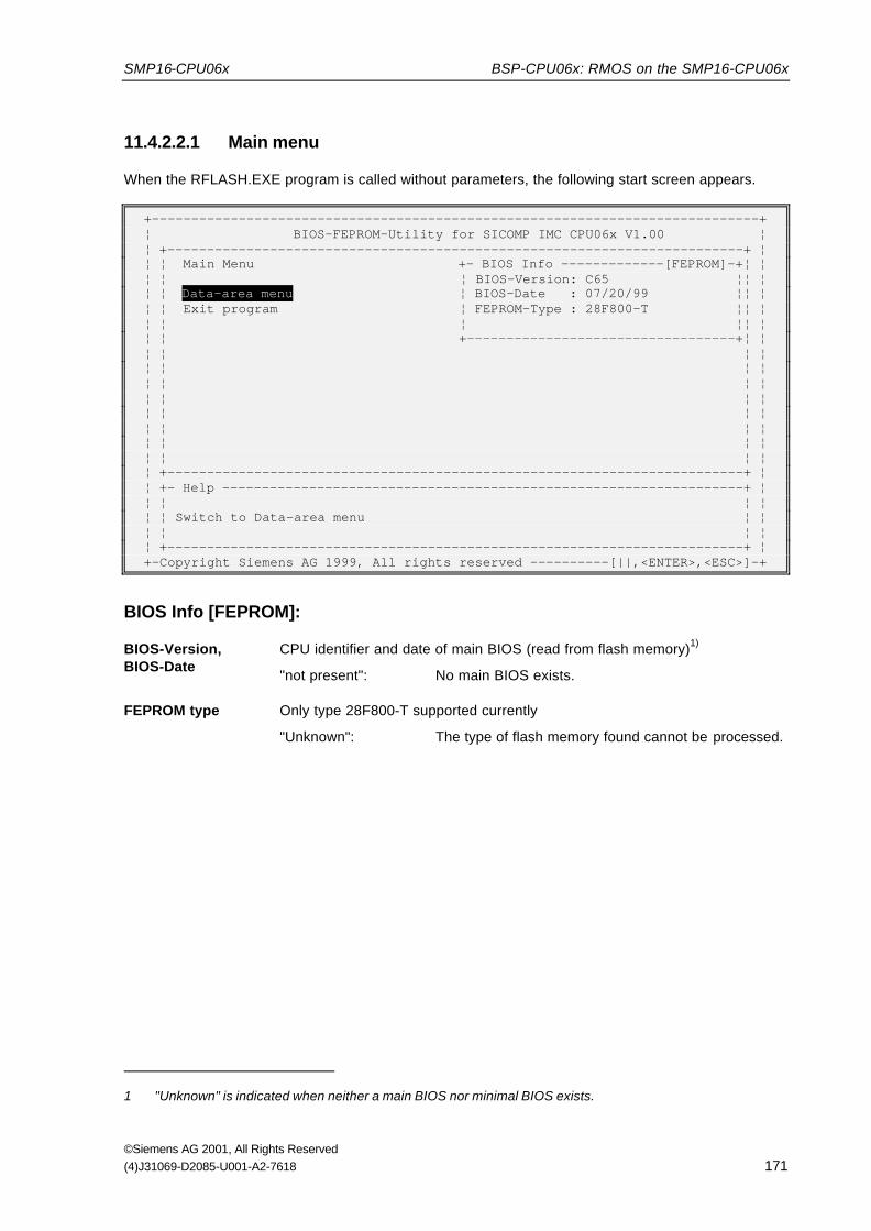
SMP16-CPU06x BSP-CPU06x: RMOS on the SMP16-CPU06x
©Siemens AG 2001, All Rights Reserved(4)J31069-D2085-U001-A2-7618 171
11.4.2.2.1 Main menu
When the RFLASH.EXE program is called without parameters, the following start screen appears.
+-----------------------------------------------------------------------------+¦ BIOS-FEPROM-Utility for SICOMP IMC CPU06x V1.00 ¦¦ +-------------------------------------------------------------------------+ ¦¦ ¦ Main Menu +- BIOS Info -------------[FEPROM]-+¦ ¦¦ ¦ ¦ BIOS-Version: C65 ¦¦ ¦¦ ¦ Data-area menu ¦ BIOS-Date : 07/20/99 ¦¦ ¦¦ ¦ Exit program ¦ FEPROM-Type : 28F800-T ¦¦ ¦¦ ¦ ¦ ¦¦ ¦¦ ¦ +----------------------------------+¦ ¦¦ ¦ ¦ ¦¦ ¦ ¦ ¦¦ ¦ ¦ ¦¦ ¦ ¦ ¦¦ ¦ ¦ ¦¦ ¦ ¦ ¦¦ ¦ ¦ ¦¦ ¦ ¦ ¦¦ +-------------------------------------------------------------------------+ ¦¦ +- Help ------------------------------------------------------------------+ ¦¦ ¦ ¦ ¦¦ ¦ Switch to Data-area menu ¦ ¦¦ ¦ ¦ ¦¦ +-------------------------------------------------------------------------+ ¦+-Copyright Siemens AG 1999, All rights reserved ----------[||,<ENTER>,<ESC>]-+
BIOS Info [FEPROM]:
BIOS-Version,BIOS-Date
CPU identifier and date of main BIOS (read from flash memory)1)
"not present": No main BIOS exists.
FEPROM type Only type 28F800-T supported currently
"Unknown": The type of flash memory found cannot be processed.
1 "Unknown" is indicated when neither a main BIOS nor minimal BIOS exists.

BSP-CPU06x: RMOS on the SMP16-CPU06x SMP16-CPU06x
©Siemens AG 2001, All Rights Reserved172 (4)J31069-D2085-U001-A2-7618
11.4.2.2.2 Data Area Menu
The commands in this menu can be used to move the user data in the data area between flashmemory and floppy disk/hard disk.
+-----------------------------------------------------------------------------+¦ BIOS-FEPROM-Utility for SICOMP IMC CPU06x V1.00 ¦¦ +-------------------------------------------------------------------------+ ¦¦ ¦ Data-Area Menu +- Data-Area Info --------[FEPROM]-+¦ ¦¦ ¦ ¦ [00000]: xx xx xx xx xx xx xx xx ¦¦ ¦¦ ¦ Clear FEPROM ¦ [00008]: xx xx xx xx xx xx xx xx ¦¦ ¦¦ ¦ Write FEPROM to file ¦ [00010]: xx xx xx xx xx xx xx xx ¦¦ ¦¦ ¦ Write file to FEPROM ¦ [00018]: xx xx xx xx xx xx xx xx ¦¦ ¦¦ ¦ Back to main menu ¦ [00020]: xx xx xx xx xx xx xx xx ¦¦ ¦¦ ¦ ¦ [00028]: xx xx xx xx xx xx xx xx ¦¦ ¦¦ ¦ ¦ [00030]: xx xx xx xx xx xx xx xx ¦¦ ¦¦ ¦ ¦ [00038]: xx xx xx xx xx xx xx xx ¦¦ ¦¦ ¦ ¦ [00040]: xx xx xx xx xx xx xx xx ¦¦ ¦¦ ¦ ¦ [00048]: xx xx xx xx xx xx xx xx ¦¦ ¦¦ ¦ ¦ [00050]: xx xx xx xx xx xx xx xx ¦¦ ¦¦ ¦ +--------------[<g>,<PGUP>,<PGDN>]-+¦ ¦¦ ¦ ¦ ¦¦ +-------------------------------------------------------------------------+ ¦¦ +- Help ------------------------------------------------------------------+ ¦¦ ¦ ¦ ¦¦ ¦ Clears Data-area within the BIOS-FEPROM ¦ ¦¦ ¦ ¦ ¦¦ +-------------------------------------------------------------------------+ ¦+-Copyright Siemens AG 1999, All rights reserved ----------[||,<ENTER>,<ESC>]-+
Menu commands
Clear FEPROM Deletes the entire data area in flash memory
Write FEPROM tofile
Reads the current data area from flash memory and writes the data in a file
Write file toFEPROM
Reads the contents of a file and writes them to the data area in flash memoryIf the area already contains data, these data must be deleted beforehand.
Indicating the data area
Page-Up,Page-Down
Pages through the indicated data area from flash memory
g (go) Entry of an offset value to jump back and forth throughout the entire data area(0h to BFFFFh)
Layout of a data area file
A data area file is a binary file with a maximum length of 768 kbytes. It can contain any data.

SMP16-CPU06x BSP-CPU06x: RMOS on the SMP16-CPU06x
©Siemens AG 2001, All Rights Reserved(4)J31069-D2085-U001-A2-7618 173
11.4.2.2.3 Call Parameters
When the USER DATA update utility is called with the command line parameters, the menu-prompteduser interface is not shown. All operations are then controlled by the parameters.
Parameters Meaning
/? Indicates a help page with explanations of the available parameters
/I Indicates information on the current BIOS in flash memory
/DC Deletes the data area from flash memory
/DL<filename> Loads the data area from the specified file to flash memory1)
/DS<filename> Backs up the data area from flash memory to the specified file
1) Flash memory must be deleted beforehand.
Several parameters can be specified in one call. These parameters are then executed in succession.The command line may not exceed 128 characters.
Note:The actions are the same as the menu commands of the user interface with the following exceptions.
• No "are you sure" query is made before writing to flash memory.
• When an error occurs, the program is terminated and the other commands specified are notexecuted.
Files names must immediately follow (no blanks) the command and may not be longer than 17characters. Since this length will definitely not be sufficient to enter absolute paths, we recommendaccessing the program with the MS-DOS path and then executing it from the directory containing thedesired files.
Example
BIOSUP /I /DSuser_old.bin /DLuser_new.bin
• Information on the BIOS in flash memory is displayed on the monitor screen.
• The old user data are backed up with the /DS option in the USER_OLD.BIN file.
• The user data are loaded with the /DL option from the USER_NEW.BIN file to flash memory.
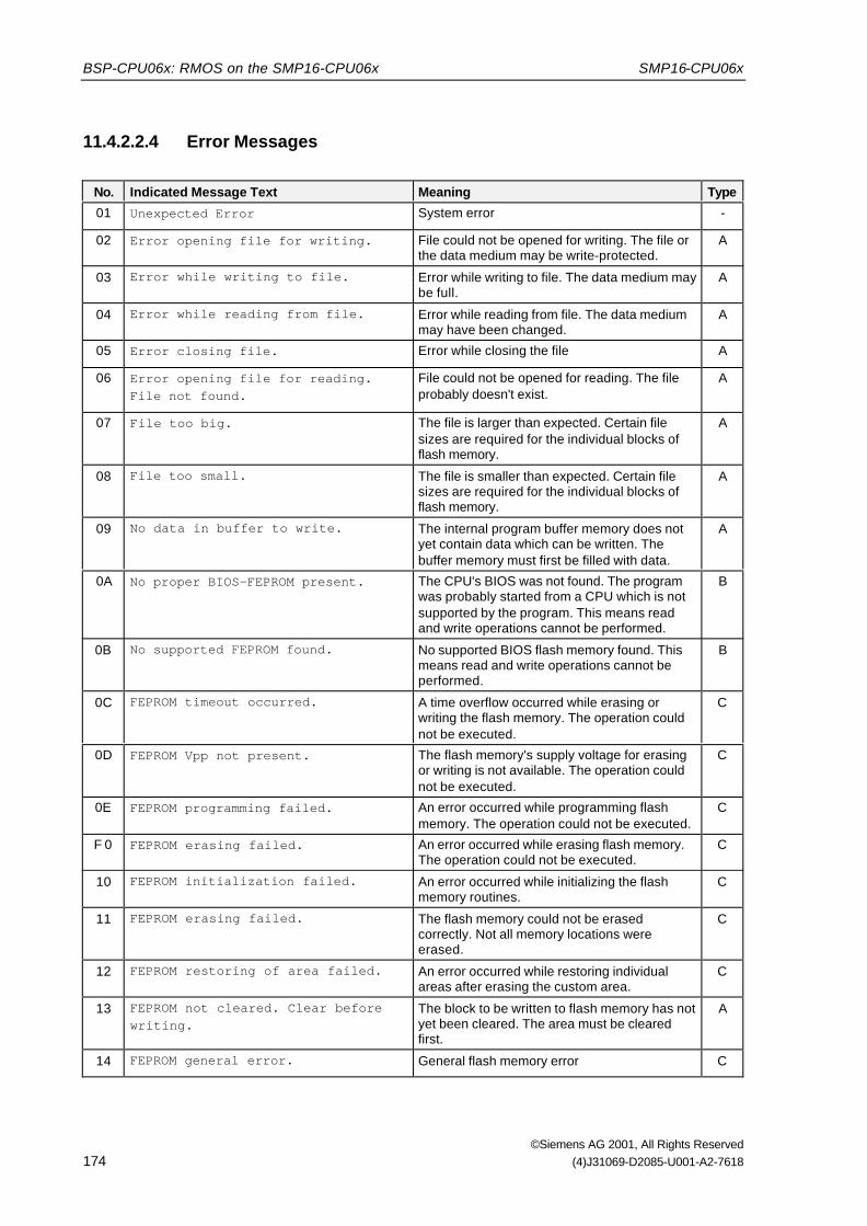
BSP-CPU06x: RMOS on the SMP16-CPU06x SMP16-CPU06x
©Siemens AG 2001, All Rights Reserved174 (4)J31069-D2085-U001-A2-7618
11.4.2.2.4 Error Messages
No. Indicated Message Text Meaning Type
01 Unexpected Error System error -
02 Error opening file for writing. File could not be opened for writing. The file orthe data medium may be write-protected.
A
03 Error while writing to file. Error while writing to file. The data medium maybe full.
A
04 Error while reading from file. Error while reading from file. The data mediummay have been changed.
A
05 Error closing file. Error while closing the file A
06 Error opening file for reading.File not found.
File could not be opened for reading. The fileprobably doesn't exist.
A
07 File too big. The file is larger than expected. Certain filesizes are required for the individual blocks offlash memory.
A
08 File too small. The file is smaller than expected. Certain filesizes are required for the individual blocks offlash memory.
A
09 No data in buffer to write. The internal program buffer memory does notyet contain data which can be written. Thebuffer memory must first be filled with data.
A
0A No proper BIOS-FEPROM present. The CPU's BIOS was not found. The programwas probably started from a CPU which is notsupported by the program. This means readand write operations cannot be performed.
B
0B No supported FEPROM found. No supported BIOS flash memory found. Thismeans read and write operations cannot beperformed.
B
0C FEPROM timeout occurred. A time overflow occurred while erasing orwriting the flash memory. The operation couldnot be executed.
C
0D FEPROM Vpp not present. The flash memory's supply voltage for erasingor writing is not available. The operation couldnot be executed.
C
0E FEPROM programming failed. An error occurred while programming flashmemory. The operation could not be executed.
C
F 0 FEPROM erasing failed. An error occurred while erasing flash memory.The operation could not be executed.
C
10 FEPROM initialization failed. An error occurred while initializing the flashmemory routines.
C
11 FEPROM erasing failed. The flash memory could not be erasedcorrectly. Not all memory locations wereerased.
C
12 FEPROM restoring of area failed. An error occurred while restoring individualareas after erasing the custom area.
C
13 FEPROM not cleared. Clear beforewriting.
The block to be written to flash memory has notyet been cleared. The area must be clearedfirst.
A
14 FEPROM general error. General flash memory error C

SMP16-CPU06x BSP-CPU06x: RMOS on the SMP16-CPU06x
©Siemens AG 2001, All Rights Reserved(4)J31069-D2085-U001-A2-7618 175
No. Indicated Message Text Meaning Type
15 Parameter error. (use /? for help). Wrong command line parameter K
Types of messages
A: Error during data handling. Usually an operator error.
B: Program doesn't support CPU board.
C: Flash memory error. Shouldn't occur during normal operation. Repeat action.
K: Error only with command line version

BSP-CPU06x: RMOS on the SMP16-CPU06x SMP16-CPU06x
©Siemens AG 2001, All Rights Reserved176 (4)J31069-D2085-U001-A2-7618
11.4.3 Use of the Serial EEPROM
The board is equipped with a 256-byte EEPROM for storing configuration data. The contents of thischip are retained even without battery backup after the supply voltage is turned off. The first 64 bytesare reserved for manufacturer data and may not be overwritten.
Attention:The EEPROM is designed for 1 million write-accesses.
Note:The functions do not check to determine whether the maximum number of write-accesses hasalready been reached. The calls are not protected against multiple accesses (i.e., these calls shouldonly be called from one task).
11.4.3.1.1 Reading the Serial EEPROM - RcReadSerEEPROM
Function Reads the serial EEPROM
Include file <rccpu06x.h>
Syntax int FEPROMRead (unsigned int FEPROMAdrOffset,unsigned int Length,unsigned char * Buffer);
Parameter Name Meaning
EEPROMAdrOffset Start address of the bytes to be read (0h, ... C3h)
Length Number of bytes to be read
Buffer Pointer to the DRAM memory area for writing theread data
Description Reads a certain number of bytes from the serial EEPROM
Return value 0 Conclusion successful
-1: Write error
-2 Invalid address (EEPROMAdrOffset is greater than )196
-3 Invalid length (Length is greater than )196
-4 Invalid buffer (buffer is ZERO)

SMP16-CPU06x BSP-CPU06x: RMOS on the SMP16-CPU06x
©Siemens AG 2001, All Rights Reserved(4)J31069-D2085-U001-A2-7618 177
11.4.3.1.2 Writing the Serial EEPROM - RcWriteSerEEPROM
Function Writes the serial EEPROM
Include file <rccpu06x.h>
Syntax int FEPROMRead (unsigned int FEPROMAdrOffset,unsigned int Length,unsigned char * Buffer);
Parameter Name Meaning
EEPROMAdrOffset Start address of the bytes to be written (0h, ..., C3h)
Length Number of bytes to be written
Buffer Pointer to the DRAM memory area with the data to bewritten
Description Writes a certain number of bytes to the serial EEPROM
Return value 0 Conclusion successful
-1: Write error
-2 Invalid address (EEPROMAdrOffset is greater than )196
-3 Invalid length (Length is greater than )196
-4 Invalid buffer (buffer is ZERO)
11.4.3.1.3 Determining the Size of the Serial EEPROM -RcGetMaxLengthSerEEPROM
Function Determines the size of the serial EEPROM
Include file <rccpu06x.h>
Syntax Int RcGetMaxLengthSerEEPROM (unsigned int * Length);
Parameter Name Meaning
Length Size of the serial EEPROM
Description Returns the size of the serial EEPROM
Return value 0 Conclusion successful
-1: Write error
-2 Invalid address (EEPROMAdrOffset is greater than )196
-3 Invalid length (Length is greater than )196
-4 Invalid buffer (buffer is ZERO)

BSP-CPU06x: RMOS on the SMP16-CPU06x SMP16-CPU06x
©Siemens AG 2001, All Rights Reserved178 (4)J31069-D2085-U001-A2-7618
11.4.4 Use of the Buffered SRAM
The driver emulates an SRAM disk. It is registered with HSFS (High Speed File System) so that themedium can be used as a logical drive (R0:). If not already formatted, the SRAM disk is formattedautomatically by the driver during startup. The following message appears during RMOS startup if thememory hole is not enabled.
NUC: Memory Hole disabled in Bios SetupNUC: SRAM-Driver not loaded
The driver can only be used in an RMOS3-PC1 system (V3.20).
11.4.4.1 Organization of the Tasks/Functions
The driver is only the SVC portion of a driver. It is not an interrupt-driven driver. It is implemented as adriver so that it can be registered with HSFS (i.e., so that the SRAM disk can be addressed as alogical drive).

SMP16-CPU06x BSP-CPU06x: RMOS on the SMP16-CPU06x
©Siemens AG 2001, All Rights Reserved(4)J31069-D2085-U001-A2-7618 179
Overview
Treiberkonfiguration
RMOS-Treiber
Initialiserung im Anlauf
SVC-Teil
SRAM- Zugriffsfunktionen
HW
SVC
TreiberHSFS
Anwender Supportfunktionen
SVC
- Initialisierung für HSFS (VIB)
(über CRUN))
VIBs
Unterstützende Funktionen
Treiberbestandteile
Figure 11.1 Structure of the RMOS driver/functions
The HSFS handles the logical management of the memory as a drive. The HSFS also handlesformatting.
Driver
Driverconfiguration SRAM access
functions
RMOS driver
Initializationduring startup
SVC portion
Support functions- Initialization for HSFS (VIB)
(Via CRUN)
User
Supporting functions
Driver components

BSP-CPU06x: RMOS on the SMP16-CPU06x SMP16-CPU06x
©Siemens AG 2001, All Rights Reserved180 (4)J31069-D2085-U001-A2-7618
11.4.4.2 Driver Configuration Blocks
Tables are used to configure the driver (device) and its units.
• DCD (Device Control Data)
• UCDs (Unit Control Data)
The tables are required when the driver is linked to RMOS.
The layout of the tables will now be described.
11.4.4.2.1 Device Control Data Table (DCD)
Driver-related configurations are specified in the DCD (Device Control Data).
Table 11.1 Layout of the DCD
Parameters Description Type Standard Value
ucd Address of the first UCD structure for thisdriver
Near pointer toRmUCDStruct
1)
units Number of units for this driver uchar 1)
shr ID of another DCD which this controller alsouses (FFh if none)
uchar 0xFF 1)
init Entry point of the initialization routine rmproc 2)
svc RIO SVC entry point for this driver rmproc 3)
flags Driver flagsBit 0=1 Parallel driverBit 1=1: Type II driverBit 2=0: Initialization while booting
uchar 0 x 03
fmax Maximum operation code for type II driver uchar 0xF
reserv 2 reserved bytes uchar 0 x 00
1) This value is used by RMOS.2) X_RD40_INI_UCB for the RMOS driver
3) X_RD40_SVC_BR for the RMOS driver
The DCD block is set up in the RCCPU06x.C file.

SMP16-CPU06x BSP-CPU06x: RMOS on the SMP16-CPU06x
©Siemens AG 2001, All Rights Reserved(4)J31069-D2085-U001-A2-7618 181
11.4.4.2.2 Device Control Data Table (UCD)
Type definition for UCD
typedef struct UCD_RD40_SUCD_HEAD head;UCD_RD40_TYPE type;UCD_RD40_COMMON com;
UCD_RD40;
The UCDs are set up in the RCCPU06x.C file.
The driver-related parameters are located in the UCD block starting at port. The following parametersmust be specified for unit 0.
Table 11.2 Parameters in UCD_HEAD
Parameters Description Type Standard Value
pid ID of the process which handles the unit uchar 0
intno Interrupt number uchar 0
int_adr Address of the interrupt handling routine rmfarproc (void *)0
uns Task ID which is started after anunexpected interrupt
ushort -1
Table 11.3 Parameters in UCD_RD40_TYPE
Parameters Description Type
start_adr Physical start address of the memory area ulong
size Size in Kbytes of the drive memory ushort
The driver sets up a descriptor based on start_adr and size. This descriptor is used to access thememory within the driver. The predefined values for the SMP16-CPU06x should be used for start_adrand size.
Table 11.4 Parameters in UCD_RD40_COMMON
Parameters Description Type
srb_border SRB threshold value uint
srb_time Wait time when the SRB threshold value is passed below uint

BSP-CPU06x: RMOS on the SMP16-CPU06x SMP16-CPU06x
©Siemens AG 2001, All Rights Reserved182 (4)J31069-D2085-U001-A2-7618
srb_border
The RMOS driver operations are executed sequentially in the RMOS-S state. Since extensiveread/write operations may require a great deal of time, the S state waiting queue may overflow.Parameter srb_border specifies how many SRBs must still be free in the RMOS waiting queue so thata read/write operation can be processed. If not enough SRBs are free, the RMOS driver stopsprocessing the read/write operation for srb_time time and then checks the number again until enoughSRBs are available again to the system. Processing is then continued.
When 0 is entered for srb_border, the RMOS driver calculates the threshold value during systemstartup. The SRB threshold value is calculated as shown below.
SRB threshold value = X_SRB_NUM – X_VECTORS_NUM
X_SRB_NUM Number of SRBs specified in the software configuration
X_VECTORS_NUM Assembler determines this parameter when the RMOS software configurationis compiled. The parameter can be viewed in a listing. It is the sum of allhardware and software interrupts.
When a value other than 0 is entered for srb_border, this value is used as is for the threshold value.
srb_time
This parameter specifies after how many milliseconds the RMOS driver is to interrupt a read/writeoperation when the SRB threshold value is violated. When 0 is entered for UCD_SRB_TIME, theRMOS driver calculates the wait time during system startup as shown below.
srb_time = 2 x (X_SRB_NUM – SRB threshold value)
If a value other than 0 is entered for UCD_SRB_TIME, this value is used as is as the wait time.

SMP16-CPU06x BSP-CPU06x: RMOS on the SMP16-CPU06x
©Siemens AG 2001, All Rights Reserved(4)J31069-D2085-U001-A2-7618 183
11.4.4.3 Driver Service Functions
Input/output requests to the driver are initiated with the RmIO system call. During softwareconfiguration, the driver receives a device ID. All RmIOs assigned to the driver must use this ID.
The driver is located in the R3CPU06x.LIB library in directory LIB\CADUL.
SYNTAX for RmIO system call
#include <rmapi.h>int RmIO(
uint Function,uint DeviceID,uint UnitID,uint Flagid,uint FlagMask,RmIOStatusStruct *pState,void *pParam);
See the RMOS documentation for the parameters of RmIO.
Table 11.5 RmIO parameter "function"
Bit Value Meaning
70
1
Preemptive bitArrange I/O request in the order of priority
Place I/O request at the beginning of the waiting queue
6
01
Wait bit
Wait for end of the I/O operationNo waiting
5, 4 Reserved
3 to 0 0 to 15 Operation code (see below)
Table 11.6 Operation code for RmIO parameter "function"
Operation Code Define Meaning
0x00 RD40_RESERVE Reserve device unit
0 x 01 RD40_FREE Enable device unit
0 x 02 RD40_READ_ONE Read one logical block
0 x 03 RD40_WRITE_ONE Write one logical block
0 x 04 RD40_FORMAT Format (empty function)
0 x 05 RD40_READ_MORE Read logical blocks
0 x 06 RD40_WRITE_MORE Write logical blocks
0 x 07 Reserved
0 x 08 Reserved
0 x 09 Reserved
0x0A Reserved
0x0B Reserved
0x0C Reserved
0x0D Reserved
0x0E RD40_IOCTRL Input/output control function

BSP-CPU06x: RMOS on the SMP16-CPU06x SMP16-CPU06x
©Siemens AG 2001, All Rights Reserved184 (4)J31069-D2085-U001-A2-7618
Table 11.6 Operation code for RmIO parameter "function"
Operation Code Define Meaning
0x0F Reserved
When a function code is invalid, the driver does not execute the I/O request and returns an error code(-1) in the primary status byte.
The RD40_IOCTRL function is divided further into suboperations. These suboperations are adapted tothe requirements of the SRAM driver.
Table 11.7 Suboperations for operation code
Suboperation Define Meaning
0x00 RD40_GET_PARAM Read operational parameters
0 x 01 Reserved
0 x 02 RD40_IDENT Determine size of the partition. Only the size parameterfrom the UCD is returned here converted into bytes.
RmIO parameter pState
During the RIO system call, a pointer to a type RmIOStatusStruct structure is transferred with thepState parameter. The driver stores in this field the status after execution of the applicable job. Thestatus field should be evaluated after each job. It is not sufficient to only check an RmIO system callwith the return value since the nucleus only stores information on the correctness of the parametershere (i.e., this provides no information on the status after the RmIO system call was processed).
With several pseudo parallel RmIO system calls (bit 6 in the Function parameter), each call must haveits own status field in which the parameters can be returned.
The first byte in the status field is the primary status byte. The second byte is the secondary statusbyte. The other bytes are combined into word groups and called 2nd status word (for RMOS2) or 3rdand 4th status word (for RMOS3). The following table explains the codes for the primary andsecondary status bytes and for the 2nd or 3rd and 4th status words for the RD40 driver.
Table 11.8 Meaning of the errors of the RD40 driver
PrimaryStatus Byte
SecondaryStatus Byte
2nd StatusWord
3rd and 4thStatusWords
Meaning
0 0 x 00 0 x 0000 0 x 0000
0 x 0000
The I/O request is in the waiting queue.
1 0 x 00 0 x 0000 0 x 00000 x 0000
The I/O request is being processed.
2 0 x 00 0 x 0000 0 x 00000 x 0000
The I/O request was concluded successfully.
-1 0 x 00 0 x 0000 0 x 00000 x 0000
I/O request returned due to invalid parameterassignment
-2 0 x 00 0 x 0000 0 x 0000
0 x 0000
Reservation/release operation was not executed sincethe device is already reserved or not reserved.
-3 0 x 00 0 x 0000 0 x 0000
0 x 0000
No partition exists. Parameter size or addr in UCD is 0.

SMP16-CPU06x BSP-CPU06x: RMOS on the SMP16-CPU06x
©Siemens AG 2001, All Rights Reserved(4)J31069-D2085-U001-A2-7618 185
Table 11.8 Meaning of the errors of the RD40 driver
PrimaryStatus Byte
SecondaryStatus Byte
2nd StatusWord
3rd and 4thStatusWords
Meaning
-4 0 x 00 0 x 0000 0 x 0000
0 x 0000
Reserved
-5 0 x 00 0 x 0000 0 x 0000
0 x 0000
Write error. An error was detected while writing. Withwrite operations, the driver checks success by readingback and verifying.
Table 11.9 Defines for status indications
Value Define
0 RD40_STS_QUEUE
1 RD40_STS_BUSY
2 RD40_STS_SUCCESS
-1 RD40_STS_ WRONG_PARAM
-2 RD40_STS_BAD_RSVR
-3 RD40_STS_PART_NOT_EXIST
-4 Reserved
-5 RD40_STS_READ_WRITE_ERROR
11.4.4.3.1 Reserving a Device Unit
Operation code: 0x00
This operation reserves the unit specified in the RmIO system call exclusively for RmIOs of the callingtask. RmIOs of other tasks are accepted but are not executed until after the unit is released. RmIOswith a set preemptive bit are an exception. I/O requests to a reserved unit are processed in a fixedsequence.
1. Calls with the set preemptive bit - in time sequence
2. Calls of the task which reserved the unit - in time sequence
3. Calls of other tasks - in the order of priority after release of the unit
If a task attempts to reserve the same unit again without previous release, an error message (-2) isstored in the primary status byte. The previous reservation is retained.
Parameter block: Not required

BSP-CPU06x: RMOS on the SMP16-CPU06x SMP16-CPU06x
©Siemens AG 2001, All Rights Reserved186 (4)J31069-D2085-U001-A2-7618
11.4.4.3.2 Enabling a Device Unit
Operation code: 0 x 01
This operation cancels the reservation of the unit specified in the RmIO system call. I/O requestswhich were blocked by the reservation can now executed in the order of their priority. If the taskattempts to release a unit which was not reserved by it before or was already released, an error code(-2) is returned in the primary status byte.
Parameter block: Not required
11.4.4.3.3 Reading One Logical Block
Operation code: 0 x 02
This operation transfers one logical block (512 bytes) from a unit to a read buffer. The logical block isread starting at the logical block address specified in the parameter block.
Parameter block:
Parameters Description Type
lba Logical block address ulong
buf_adr Address of the read buffer void _FAR *
reserve Reserved ushort
An incorrect logical block address causes the operation to be terminated with an error code (-1) in theprimary status byte.
If no SRAM exists, the primary status byte contains error code -5 after the termination.
Type definition: RD40_READ_ONE_TYP
11.4.4.3.4 Writing One Logical Block
Operation code: 0 x 03
This operation transfers one logical block (512 bytes) from a write buffer to a unit. The logical block iswritten starting at the logical block address specified in the parameter block.
Parameter block:
Parameters Description Type
lba Logical block address ulong
buf_adr Address of the write buffer void _FAR *
reserve Reserved ushort
The write buffer contains the data to be transferred. An incorrect logical block address causes theoperation to be terminated with an error code (-1) in the primary status byte.
Type definition: RD40_WRITE_ONE_TYP

SMP16-CPU06x BSP-CPU06x: RMOS on the SMP16-CPU06x
©Siemens AG 2001, All Rights Reserved(4)J31069-D2085-U001-A2-7618 187
11.4.4.3.5 Formatting
Operation code: 04 h
This operation does nothing. It is only implemented for RMOS compatibility. Unformatted SRAM isautomatically formatted with the x_rd40_init() function when the drivers are linked. This is why thex_rd40_init() function is called during startup.
Parameter block: Not required
11.4.4.3.6 Reading Logical Blocks
Operation code: 0 x 05
This operation transfers one or more logical blocks (512 bytes) from a unit to a read buffer. The logicalblocks are read starting at the logical block address specified in the parameter block.
Parameter block:
Parameters Description Type
lba Logical block address ulong
buf_adr Address of the read buffer void _FAR *
num_blk Number of blocks ushort
An incorrect logical block address causes the operation to be terminated with an error code (-1) in theprimary status byte.
If no SRAM exists, the primary status byte contains error code -5 after the termination.
Type definition: RD40_READ_MORE_TYP
11.4.4.3.7 Writing Logical Blocks
Operation code: 0 x 06
This operation transfers one or more logical blocks (512 bytes) from a write buffer to a unit. The logicalblocks are written starting at the logical block address specified in the parameter block.
Parameter block:
Parameters Description Type
lba Logical block address ulong
buf_adr Address of the write buffer void _FAR *
num_blk Number of blocks ushort
The write buffer contains the data to be transferred. An incorrect logical block address causes theoperation to be terminated with an error code (-1) in the primary status byte.
Type definition: RD40_WRITE_MORE_TYP

BSP-CPU06x: RMOS on the SMP16-CPU06x SMP16-CPU06x
©Siemens AG 2001, All Rights Reserved188 (4)J31069-D2085-U001-A2-7618
11.4.4.3.8 Input/Output Control Operation
Operation code: 0x0E
Parameter block:
Parameters Description Type
sub_fct Suboperation ushort
byte_num Assignment depends on thesuboperation.
ushort
buf_adr Assignment depends on thesuboperation.
void _FAR*
reserve Reserved ushort
Suboperation:
Suboperation Meaning
0x00 Read operational parameters
0 x 01 Reserved
0 x 02 Determines size of the partition (from UCD)
Type definition: RD40_IOCTRL_TYP
11.4.4.3.8.1 Reading Operational Parameters
Suboperation: 0x00
This suboperation reads the current operational parameter data of a unit assigned to the RMOS driver.The parameters are stored in a buffer. The address of the buffer is transferred in the parameter block.
Parameter block:
Parameters Description Type
sub_fct Suboperation (0x00) ushort
byte_num Reserved ushort
buf_adr Address of the input buffer RD40_IO_GET_PARAM FAR *
reserve Reserved ushort

SMP16-CPU06x BSP-CPU06x: RMOS on the SMP16-CPU06x
©Siemens AG 2001, All Rights Reserved(4)J31069-D2085-U001-A2-7618 189
Type definition for RD40_IO_GET_PARAM
typedef struct RD40_IO_GET_PARAM_Sushort unit_cnt;UCD_RD40_COMMON ucd_com;UCD_RD40_TYPE ucd_type;UCB_RD40_TYPE ucb_type;
RD40_IO_GET_PARAM;
Type definition for UCB_RD40_TYPE
typedef struct ulong part_length;uchar _FAR *disk_start_adr;uchar _FAR *buf_adr;ulong act_adr;ulong end_adr;uchar (*rw_funct)();
UCB_MC2OS_TYPE;
Layout of UCB_RD40_TYPE
Parameters Description Type
part_length Size in bytes of the memory areamanaged by the driver. Is calculatedfrom the size parameter of UCD(size*1024).
ulong
disk_start_adr Pointer to the beginning of the memoryarea. This pointer was requested byRMOS and is valid for part_length.
uchar _FAR *
buf_adr Buffer address of a running RmIO call uchar _FAR *
act_adr Current disk read/write address ulong
end_adr End address of a read/write function ulong
rw_funct Pointer to current RmIO read/writefunction (near pointer)
char *
11.4.4.3.8.2 Determining the Size of the Partition
Suboperation: 0 x 02
Parameter block:
Parameters Description Type
sub_fct Suboperation (0x02) ushort
Reserved ushort
part_length Address of the input buffer ulong *
reserved Reserved ushort
When called, this suboperation transfers a pointer to a 32-bit word (in the parameter block) in whichthe partition size parameterized in the driver is returned in bytes in the parameter block. The value istaken from the size (size*1024) parameterized in the UCD. This value can be used, for instance, toformat the disk.

BSP-CPU06x: RMOS on the SMP16-CPU06x SMP16-CPU06x
©Siemens AG 2001, All Rights Reserved190 (4)J31069-D2085-U001-A2-7618
11.4.4.4 System Function x_rd40_init
The SRAM disk cannot be used as a logical drive under RMOS V3.20 unless the RMOS driver has aninterface defined by HSFS. The driver can then be registered with the HSFS and addressed as alogical drive via the HSFS.
Note:System function x_rd40_init is called from RcInitSRAMenv.
A VIB (Volume Identification Block) must be created for each logical drive. The createvib call of theCRUN library is used for this. This function transfers, among others, the data carrier designation (e.g.,B: 'R0'), device ID and unit ID to the HSFS.
These VIBs are created in system function x_rd40_init.
Function Linking in all units of the driver in the HSFS
Include file <rd40.h>
Syntax int x_rd40_init(uint console_flag);
Parameter Name Meaning
console_flag 0 (= FALSE). No output of the messages.
1 (= TRUE). Output of the messages on the system console.
Description The function creates a VIB for each unit of the specified driver. The VIBs areused with the HSFS. The initialization function must be called once aftersystem reset. When the VIBs are set up, a check is made to determinewhether the drive is already formatted. If not, an attempt is made to format it(only possible with SRAM disk). The disk is formatted with the size defined inthe UCD of the driver. The disk size used for formatting depends on thememory size (e.g., 128 Kbytes for SRAM) specified in the driver UCD. Twobytes in the boot sector (i.e.,1st sector) are scanned to determine whether thedisk is already formatted. The disk is formatted when byte 0 = 0xEB and byte2 = 0x90.
A drive is set up.
R0: SRAM disk drive (if present)
If console_flag is set, the following message is displayed.
(c) Siemens AG, RMOS3 RD40 Initialization Vx.yPartition DOS, size: xxxxx KB, announced as: R0 (new formatted)

SMP16-CPU06x BSP-CPU06x: RMOS on the SMP16-CPU06x
©Siemens AG 2001, All Rights Reserved(4)J31069-D2085-U001-A2-7618 191
If an error occurs, the function is immediately exited with an error code. Whena partition was newly formatted, "(new formatted)" is displayed.
The required memory (e.g., for the VIB) is taken from the heap.
This function is called within RcInitSRAMenv() which can be used instead ofx_init_rd40() (see below).
Note:When parameters other than the default parameterization of the driver are tobe used, remember that a 12-bit FAT is set up during formatting. This meansthat the maximum size of the drive is limited to approx. 2043 Kbytes.
Return value Value Define Description
0 RD40_NO_ERROR Call okay
-1 RD40_ERR_NO_MEM Error during memory request. Nomore space on RMOS heap.
-2 RD40_ERR_HSFS_CREATE Error while calling createvib
-3 RD40_ERR_NO_DEVICE_INST RMOS driver not installed(correctly)
-4 Reserved
-5 RD40_ERR_HSFS_STATUS Error while callinggetvolumestatus()
-6 RD40_ERR_HSFS_VIB_EXIST An attempt was made to set up aVIB for a drive for which a VIBalready exists.
-7 RD40_ERR_RMIO Error while calling RD40 driver
-8 RD40_ERR_DEVICE Unexpected driver error
-9 RD40_ERR_UNIT_CNT Number of units wrong
-10 RD40_ERR_HSFS_REMAP Error while formatting a partition(e.g., due to no RAM)
-11 RD40_ERR_PARAM Parameter error
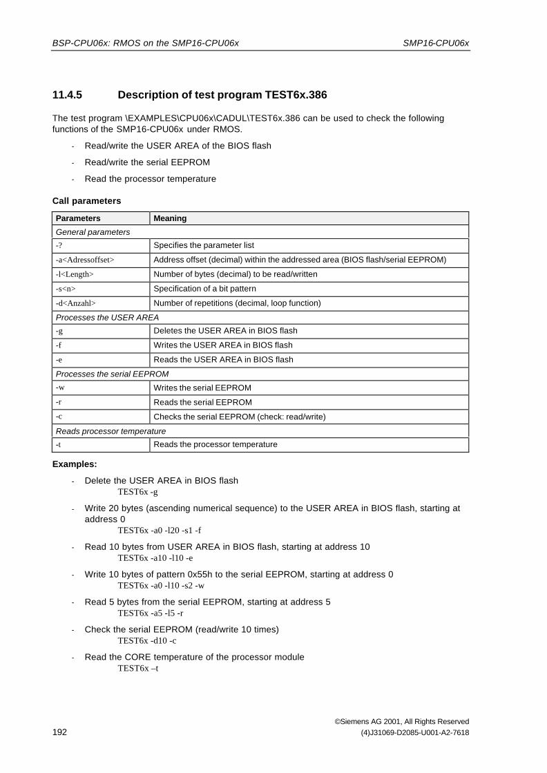
BSP-CPU06x: RMOS on the SMP16-CPU06x SMP16-CPU06x
©Siemens AG 2001, All Rights Reserved192 (4)J31069-D2085-U001-A2-7618
11.4.5 Description of test program TEST6x.386
The test program \EXAMPLES\CPU06x\CADUL\TEST6x.386 can be used to check the followingfunctions of the SMP16-CPU06x under RMOS.
- Read/write the USER AREA of the BIOS flash
- Read/write the serial EEPROM
- Read the processor temperature
Call parameters
Parameters Meaning
General parameters
-? Specifies the parameter list
-a<Adressoffset> Address offset (decimal) within the addressed area (BIOS flash/serial EEPROM)
-l<Length> Number of bytes (decimal) to be read/written
-s<n> Specification of a bit pattern
-d<Anzahl> Number of repetitions (decimal, loop function)
Processes the USER AREA
-g Deletes the USER AREA in BIOS flash
-f Writes the USER AREA in BIOS flash
-e Reads the USER AREA in BIOS flash
Processes the serial EEPROM
-w Writes the serial EEPROM
-r Reads the serial EEPROM
-c Checks the serial EEPROM (check: read/write)
Reads processor temperature
-t Reads the processor temperature
Examples:
- Delete the USER AREA in BIOS flashTEST6x -g
- Write 20 bytes (ascending numerical sequence) to the USER AREA in BIOS flash, starting ataddress 0
TEST6x -a0 -l20 -s1 -f
- Read 10 bytes from USER AREA in BIOS flash, starting at address 10TEST6x -a10 -l10 -e
- Write 10 bytes of pattern 0x55h to the serial EEPROM, starting at address 0TEST6x -a0 -l10 -s2 -w
- Read 5 bytes from the serial EEPROM, starting at address 5TEST6x -a5 -l5 -r
- Check the serial EEPROM (read/write 10 times)TEST6x -d10 -c
- Read the CORE temperature of the processor moduleTEST6x –t

SMP16-CPU06x Appendix
©Siemens AG 2001, All Rights Reserved(4)J31069-D2085-U001-A2-7618 193
12 Appendix
12.1 Notes on the Different Operating Systems
12.1.1 Windows NT
Windows NT does not support the AGP interface until service pack 3. Up to that point, only thestandard resolution of up to 800 x 600 with 16 colors can be used.
When you use the board with the WindowsNT operating system but without the SMP16 busbackplane, set "SMP16-Bus" to "Disabled" in BIOS Setup under "IMC MISCELLANEOUS" (seechapter 9.1.10).
12.1.2 Win9x
Operating systems that support power management (e.g., APM with Win9x) reset manual throttlingduring startup.
This also means that the no-fan setting is canceled in Setup.
If this happens, power management must be deactivated in the operating system (e.g., deactivate thesupport for APM in system control under Win9x).
Another method is to control throttling with a program/driver. It is important to reset the throttling rateafter a power management event (e.g., power save mode after a period of inactivity) arrives.
12.1.3 RMOS
When the SMP16-CPU06x is used with the SMP16-COM223 (DMA mode), experience has shown that"Passive Release" must be dactivated in BIOS for correct operation (see chapter 9.1.5).

Appendix SMP16-CPU06x
©Siemens AG 2001, All Rights Reserved194 (4)J31069-D2085-U001-A2-7618
12.2 Layout of the CMOS RAM and the CDT
The CMOS default table is an image of the 128-byte CMOS RAM.
Offset StartingF800:0h
CMOSRegister
Meaning
00h 00 h Time, seconds (0 to 59)
01 h 01 h Alarm time, seconds (0 to 59)
02 h 02 h Time, minutes (0 to 59)
03 h 03 h Alarm time, minutes (0 to 59)
04 h 04 h Time, hours (0 to 23)
05 h 05 h Alarm time, hours (0 to 23)
06 h 06 h Date, day of the week (1 to 7)
07 h 07 h Date, day of month (1 to 31)
08 h 08 h Date, month (1 to 12)
09 h 09 h Date, year
0Ah 0Ah Status register A (is not taken from CDT)
0Bh 0Bh Status register B (is not taken from CDT)
0Ch 0Ch Status register C (is not taken from CDT)
0Dh 0Dh Status register D (is not taken from CDT)
0Eh 0Eh Diagnosis status byte (is not taken from CDT)
0Fh 0Fh Reset code (is not taken from CDT)
10 h 10 h Floppy disk types for drive A: and B:
11 h 11 h Security flags
12 h 12 h Hard disk types
13 h 13 h Reserved
14 h 14 h Configuration byte
15 h 15 h Size of base memory (low byte)
16 h 16 h Size of base memory (high byte)
17 h 17 h Size of extended memory (low byte)
18 h 18 h Size of extended memory (high byte)
19 h 19 h Expansion byte for hard disk 0 (type 16 and higher)
1Ah 1Ah Expansion byte for hard disk 1 (type 16 and higher)
1Bh to 2Dh - Reserved
2Eh, 2Fh 2Eh, 2Fh CMOS CHECKSUM (sum of registers 10h to 2Dh,high byte in register 2Eh, low byte in register 2Fh)
30 h 30 h Size of extended memory
31 h 31 h Size of extended memory
32 h 32 h Century for date
33 h 33 h Power-on flags
34h to 77h - Reserved
Attention:As used here, "reserved" means that these memory locations are used internally by BIOS. They arestored in the CDT.

SMP16-CPU06x Appendix
©Siemens AG 2001, All Rights Reserved(4)J31069-D2085-U001-A2-7618 195
12.3 Use of the CDT during BIOS Startup
The following figure shows the interplay between CDT and CMOS RAM during system startup.
Start
Read CDT toBuffer
ChecksumOK?
Read CMOS contents
Read CMOS contents
ChecksumOK?
ChecksumOK?
Compare Buffer &CMOS
Valuesidentical
?
End
Update CDT withCMOS contents
Load Defaultsinto CMOS
Update CMOS withMirror contents
Yes
No
Yes
Yes
Yes
No
No
No
The CDT always contains the last valid contents of the CMOS RAM (i.e., the CDT is rewritten eachtime CMOS changes or the CDT is copied to CMOS when the contents of CMOS were destroyed).
Note:The only sign the user has that the contents of CMOS have been lost is a clock showing the wrongtime.

Appendix SMP16-CPU06x
©Siemens AG 2001, All Rights Reserved196 (4)J31069-D2085-U001-A2-7618
12.4 POST Codes
The following codes are output to address 80h during system startup.
Code Description
C0H Basic initialization chipset
C1H Search for ID for compressed BIOS
Determine memory configuration
0CH Test memory from 0H to 3FFFFH
Copy BIOS from 0E0000H to 0FFFFFH to 10000H to 2FFFFSet up stack
03H Check BIOS checksum
Starting here, the procedure varies. If the checksum of BIOS was okay, the standard startup iscontinued.
Code Description
C3H Decompress BIOS
C5H Copy unpacked BIOS to E and F bank
03H Save warm-start flag in BIOS data area
05H Initialize super-I/O chip, keyboard controller
06H Check whether F segment can be read/written
07 h Test CMOS RAM
08 h Program chipset with default values
09 h Initialize cache
0Ah Install interrupt default handler
0BH Check CMOS battery and checksum
Microcode update, if necessary
0CH Initialize BIOS data area for keyboard
0DH Determine CPU clock pulse
Video identifier (mono/color, mode)
0EH Test video memory
Output CPU type and clock pulse frequency
0FH Check whether PS2 mouse is supportedDMA test
14 h Counter test
15 h Test mask bit of the master interrupt controller (only for cold start)
16 h Test mask bit of the slave interrupt controller (only for cold start)
18 h Interrupt controller
19 h Test initialization of the serial port for console rerouting
30 h Look for memory up to 640 KbytesLook for memory over 1 Mbyte
31 h Test found memory
32 h Initialize on-board super-I/O
3CH Enable Setup
3DH Initialize mouse

SMP16-CPU06x Appendix
©Siemens AG 2001, All Rights Reserved(4)J31069-D2085-U001-A2-7618 197
Code Description
3EH Set IRQ12 for mouse, if present
41H Call Setup if DEL key pressedInstall floppy
42H Install hard disk
43H Check which COM and LPT interfaces are present and enterin BIOS data area
45H Initialize coprocessor
47H Enter address of boot sector buffer in BIOS data area
4FH Scan password, if activated
50H Store CMOS stack in CMOS and generate checksum
52H Initialize USBTurn on cache if enabledUnpack option ROMs
Look for BIOS extensions between C8000H and E0000H
61H Set external cache based on Setup
Rest of chipset programming
62H Disable SMP16 bus interface (if set in Setup)Set NUMLOCK and key delay based on Setup
63H ESCD updateCorrect century if necessary
FFH Call INT 19 for bootstrap
If the checksum of BIOS was wrong, a minimum BIOS is executed from the boot block of the flash.
Code Description
C3H Decompress BIOS
C5H Shadow boot block
01 h Delete lower 640 kbytes
05H Initialize keyboard
0CH Set interrupt vectors
0DH Initialize video
41H Initialize floppy controller and super-I/O chip
FFH Boot from floppy

Appendix SMP16-CPU06x
©Siemens AG 2001, All Rights Reserved198 (4)J31069-D2085-U001-A2-7618
12.5 View of the Front Plate of the SMP16-CPU06x
Figure 12.1 Front plate of the SMP16-CPU06x

SMP16-CPU06x Appendix
©Siemens AG 2001, All Rights Reserved(4)J31069-D2085-U001-A2-7618 199
Figure 12.2 Front plate of the SMP16-CPU06x with the AGP option

Appendix SMP16-CPU06x
©Siemens AG 2001, All Rights Reserved200 (4)J31069-D2085-U001-A2-7618
12.6 Abbreviations and TermsACPI Advanced Configuration Programming Interface
AGP Accelerated Graphics Port
AMS Advanced Microcomputer System
ANSI/VT 100 American National Standards Institute
APM Advanced Power Management
ARA Alert Response Address
American Standard Code for Information Interchange
AT Advanced Technology
ATA AT Attachment (connection standard for hard disks)
Baudrate Number of times a transmission channel changes states per second
BDA BIOS Data Area
BIOS Basic Input/Output System(Basic Input/Output System)
BSP Board Support Package
Cache High-speed intermediate memory used between a fast CPU and a slowmemory subsystem
CDT CMOS Default Table
CLI Command Line Interpreter
Centronics cable Connection cable for parallel printers
CMOS-RAM Static (battery-buffered) RAM
COM A, COM B Communication Port (serial interface)
CPU Central Processing Unit
CRC Cyclic Redundancy Check
CRT Cathode Ray Tube
CSMA/CD Carrier Sense Multiple Access/Collision Detect
CTS Clear To Send
DC Direct Current
DCD Device Control Data
DMA Direct Memory Access
DRAM Dynamic RAM (working storage)
DSR Data Set Ready
ECC Error Correcting Code
ECP Enhanced Cpability Port
EDO Extended Data Output
EEPROM Electrically Erasable Programmable Read Only Memory
EGB (ESD) Electrostatic Sensitive Device

SMP16-CPU06x Appendix
©Siemens AG 2001, All Rights Reserved(4)J31069-D2085-U001-A2-7618 201
EIDE Enhanced Intelligent Drive Electronics
EMV Electromagnetic compatibility
EN European standard
EP Slot
EPP Enhanced Parallel Port
ESC Escape
ESCD Extended System Configuration Data
FEPROM Flash EPROM
Flash memory EEPROM which can be erased by block
GPP General Purpose Port
HSFS High Speed File System
IDE Intelligent Drive Electronics
IEC European standard
IMC Industrial Micro Computer
IPCI Industrial PCI
IRQ Interrupt Request
ISA Industrial Standard Architecture(bus system with 8/16-bit data bus)
KSx Construction status of a board
L2-Cache Second Level Cache
LAN Local Area Network
LBA Logical Block Addressing
LED Light Emitting Diode
LPT Line Printer (parallel interface)
LSB Least Significant Bit
LVDS Low Voltage Differential Signal
MAC Media Access Controller
MMC2 Mobile Module Connector 2
MMIO Memory Mapped Input/Output
MS-DOS Microsoft Disk Operating System
MSB Most Significant Bit
NMI Non Maskable Interrupt(Non Maskable Interrupt)
PC/AT Personal Computer, Advanced Technology
PCI Peripheral Component Interconnect(bus system with 32-bit data bus)
PCSSPIC PC Soft Slave Programmable Interrupt Controller

Appendix SMP16-CPU06x
©Siemens AG 2001, All Rights Reserved202 (4)J31069-D2085-U001-A2-7618
PIC Programmable Interrupt Controller
PNP Plug and Play
Port Address in the I/O address area of the 80x86
POST Quick Power On Self Test
PS Power Supply
RAM Random Access Memory
RMIO RMOS driver call
RMOS Real Time Multitasking Operating System
RTC Real Time Clock
SCSI Small Computer Systems Interface(interface for external mass storage)
SDRAM Synchronous DRAM
SEEPROM Serial Electrically Erasable Programmable Read Only Memory
Shadowing Transmission of ROM code to a RAM. The ROM is then faded out of theaddress area, and the RAM shadows the former address area of the ROM.Used for faster accessing.
SMB System Management Bus
SMP Siemens Microcomputer PCB System
SPP Standard Printer Port
SO-DIMM Small Outline Dual-Inline Memory Module
SRAM Static Random Access Memory
SRB System Resource Block
SSPIC Soft Slave Peripheral Interrupt Controller
Sub D Sub Delta (a particular construction form for computer interfaces)
SV Power supply
SVC Supervisor Call
TCP/IP /Internet Protocol
UART Universal Asynchronous Receiver/Transmitter (blocks for serial datatransmission)
UCD Unit Control Data
VGA Video Graphics Array
VIB Volume Identification Block
WD Watchdog
WDE Watchdog Enable
WTIM Watchdog Timer
![Robust Statistics and Arrangements David Eppsteineppstein/pubs/Epp-DIMACS-03-CompStat.pdf · [Cole, Salowe, Steiger, and Szemerédi, SICOMP 1989] • Randomly chosen arrangement intersection](https://img.pdfslide.us/doc/110x75/60ad66d060981a6cb719f93c/robust-statistics-and-arrangements-david-eppsteinpubsepp-dimacs-03-compstatpdf.jpg)


![Robust Statistics and Arrangements David Eppsteineppstein/pubs/Epp-DIMACS-03...[Cole, Salowe, Steiger, and Szemerédi, SICOMP 1989] • Randomly chosen arrangement intersection [Matousek,](https://img.pdfslide.us/doc/110x75/60ad66d060981a6cb719f93e/robust-statistics-and-arrangements-david-eppstein-eppsteinpubsepp-dimacs-03.jpg)