Embed Size (px)
Citation preview

Smart Phone Control of Advanced Sensor Systems
Michigan State University College of Engineering
ECE480
Design Team 8
Steve Hilton – Manager
Micah Zastrow – Webmaster
Michael Allon– Documentation Prep
Donghun Ha– Lab Coordinator
Paul Krutty– Presentation Prep
2
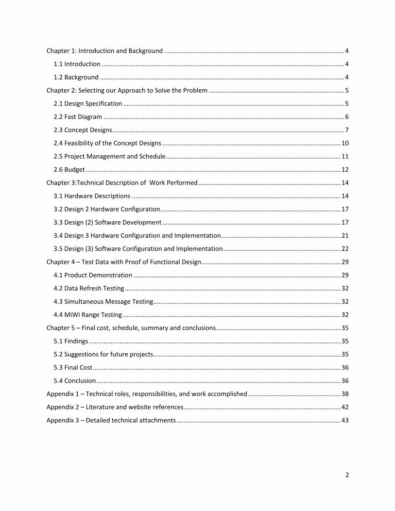
Chapter 1: Introduction and Background ..................................................................................................... 4
1.1 Introduction ........................................................................................................................................ 4
1.2 Background ......................................................................................................................................... 4
Chapter 2: Selecting our Approach to Solve the Problem ............................................................................ 5
2.1 Design Specification ............................................................................................................................ 5
2.2 Fast Diagram ....................................................................................................................................... 6
2.3 Concept Designs .................................................................................................................................. 7
2.4 Feasibility of the Concept Designs .................................................................................................... 10
2.5 Project Management and Schedule .................................................................................................. 11
2.6 Budget ............................................................................................................................................... 12
Chapter 3:Technical Description of Work Performed ................................................................................ 14
3.1 Hardware Descriptions ..................................................................................................................... 14
3.2 Design 2 Hardware Configuration ..................................................................................................... 17
3.3 Design (2) Software Development .................................................................................................... 17
3.4 Design 3 Hardware Configuration and Implementation ................................................................... 21
3.5 Design (3) Software Configuration and Implementation .................................................................. 22
Chapter 4 – Test Data with Proof of Functional Design .............................................................................. 29
4.1 Product Demonstration .................................................................................................................... 29
4.2 Data Refresh Testing ......................................................................................................................... 32
4.3 Simultaneous Message Testing ......................................................................................................... 32
4.4 MiWi Range Testing .......................................................................................................................... 32
Chapter 5 – Final cost, schedule, summary and conclusions ...................................................................... 35
5.1 Findings ............................................................................................................................................. 35
5.2 Suggestions for future projects ......................................................................................................... 35
5.3 Final Cost ........................................................................................................................................... 36
5.4 Conclusion ......................................................................................................................................... 36
Appendix 1 – Technical roles, responsibilities, and work accomplished .................................................... 38
Appendix 2 – Literature and website references ........................................................................................ 42
Appendix 3 – Detailed technical attachments ............................................................................................ 43
3
Executive Summary
Battelle Labs, has asked design team 8 to find and develop a method of controlling and monitoring four
sensors using an android based smart-phone. This report describes Team 8’s solution to this problem.
Team 8 plans to create an android application that runs on the phone, enabling the user to monitor the
sensors through a graphical user interface (GUI). The phone will be connected via Universal Serial Bus
(USB) to a development board, which is connected to a MiWi Radio Frequency Transmitter that
connects to the multiple sensors.
Acknowledgments
Team 8 would like to thank all of the following individuals involved in helping complete
this design. Without them it would not have been possible.
Dr. Christopher Ball
Prof Michael Shanblatt
Dr. Jian Ren
4
Chapter 1: Introduction and Background
1.1 Introduction
Battelle Laboratories has recently developed sensors that detect and identify various materials using
optical spectroscopy. Team 8 was challenged to find develop a method of controlling and monitoring
multiple sensors using an Android based smart-phone. The method also must be self-contained, meaning
that the sensors and phone cannot connect to wireless networks that are already in place. The phone must
be capable of wireless communication with the sensors, detecting problems, sending commands,
monitoring status, and controlling multiple sensors simultaneously. Battelle has challenged Team 8 with
making this design wireless, portable, and user friendly.
Team 8‟s solution to this problem is to create an Android application that runs on the phone, enabling the
user to monitor the sensors through a graphical user interface (GUI). This GUI will show the sensors on
the screen, and the user will be able to select each sensor individually. The GUI will also be able to
correctly monitor the status of all the sensors simultaneously. The phone will be connected via Universal
Serial Bus (USB) to an external Radio Frequency Transmitter that connects to the multiple sensors.
1.2 Background
Network Limitations
Currently, there exists no such application of the USB port. This is most likely due to the smart-phones
embedded wireless communication technologies, including cellular and Wi-Fi. All applications that are
made today either rely on cellular networks, Wi-Fi, or Bluetooth. Battelle‟s sensors may be used in
applications where there are no cellular or Wi-Fi networks; therefore we cannot use these technologies.
Also, the range of Bluetooth is only around 10 meters, which is too small for this application.
Method of Solution
Team 8‟s approach to controlling external devices with a smart-phone aims to overcome these problems
by using external Radio Frequency transceiver technology incorporated through the micro USB port that
comes standard on many smart-phones. This compact, external hardware plug-in enables the phone to
control devices without an internet network by sending commands out of the USB port. These commands
go into a micro-controller and then through the use of an RF transmitter, are wirelessly routed to the RF
receivers on the end devices. This enables the user to wirelessly control his or her device in any location,
removing the limiting need for an internet network.
We believe that this design will be successful because it will be portable, not rely on existing networks,
and user friendly. This will allow Battelle to place their sensors wherever they want, and not have to
worry about not having wireless connection. Also, the GUI will provide an easy way for anyone to be
able to pick up the phone and know exactly what is happening with no training on how to use the
application. Therefore this design could be the difference between life and death in the battlefield. The
fact that our design creates its own wireless network, and that it is extremely portable and easy to use,
provide fast and reliable way to connect the sensors. This could save valuable time in detecting and
reacting to hazardous chemicals in the air.
5
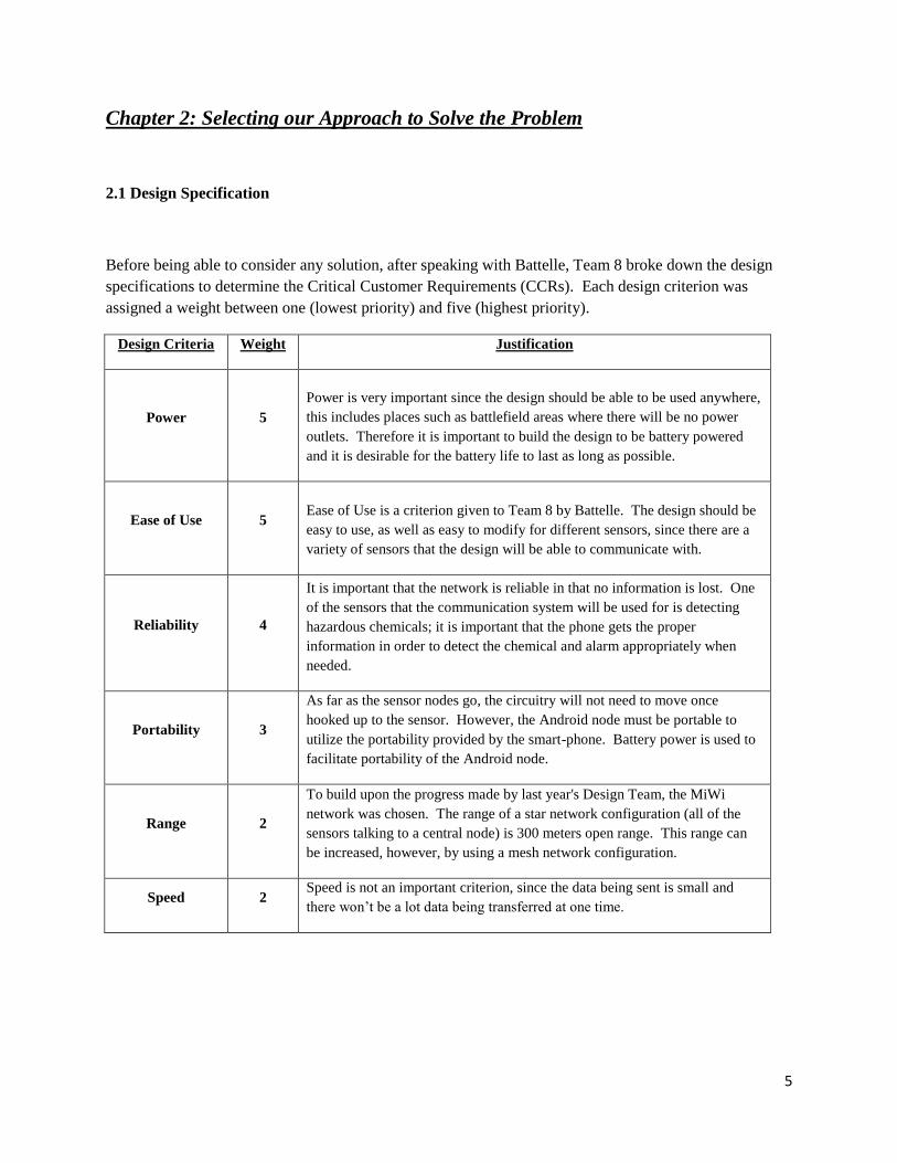
Chapter 2: Selecting our Approach to Solve the Problem
2.1 Design Specification
Before being able to consider any solution, after speaking with Battelle, Team 8 broke down the design
specifications to determine the Critical Customer Requirements (CCRs). Each design criterion was
assigned a weight between one (lowest priority) and five (highest priority).
Design Criteria Weight Justification
Power 5
Power is very important since the design should be able to be used anywhere,
this includes places such as battlefield areas where there will be no power
outlets. Therefore it is important to build the design to be battery powered
and it is desirable for the battery life to last as long as possible.
Ease of Use 5 Ease of Use is a criterion given to Team 8 by Battelle. The design should be
easy to use, as well as easy to modify for different sensors, since there are a
variety of sensors that the design will be able to communicate with.
Reliability 4
It is important that the network is reliable in that no information is lost. One
of the sensors that the communication system will be used for is detecting
hazardous chemicals; it is important that the phone gets the proper
information in order to detect the chemical and alarm appropriately when
needed.
Portability 3
As far as the sensor nodes go, the circuitry will not need to move once
hooked up to the sensor. However, the Android node must be portable to
utilize the portability provided by the smart-phone. Battery power is used to
facilitate portability of the Android node.
Range 2
To build upon the progress made by last year's Design Team, the MiWi
network was chosen. The range of a star network configuration (all of the
sensors talking to a central node) is 300 meters open range. This range can
be increased, however, by using a mesh network configuration.
Speed 2 Speed is not an important criterion, since the data being sent is small and
there won‟t be a lot data being transferred at one time.

6
Size 1
Though in the final product, the size of the Android node is ideally less than
half the size of a smart-phone. Allowing for simple portability of the central
device. Size is less important for the sensor nodes. In either case, size can
be adjusted in later designs after we prove that our conceptual design is fully
functional.
Design Criteria Weight Description
Durability 1
Durability is another design criteria that will be important in the final
product, but is not a priority in developing our prototype since we're simply
showing a proof of concept.
Security 1
Security is also an issue that we do want to work on to be able to work with
sensors that handle sensitive data. However this isn‟t an issue that is
important to get the design fully functional.
Table 2.1 Design Specification
From above, it‟s easy to discern that the most important requirements are power, ease-of-use, reliability
and portability. These requirements have been considered during the development of conceptual designs
and choosing the solution best suited for Battelle.
2.2 Fast Diagram
The Function Analysis System Technique (FAST) Diagram outlines the main functions that must be
implemented within our design, shown in Figure 2.1. It can be read from left to right or right to left with
different interpretations. Reading from left to right shows „how‟ each task is accomplished. For example,
the question “how do we interact with sensors?” can be answered by “controlling sensors” and
“monitoring sensors”. Reading from right to left shows „why‟ each task is accomplished. For example,
the question “why do we obtain commands?” can be answered by “sending commands”.

7
Figure 2.1 FAST Diagram
2.3 Concept Designs
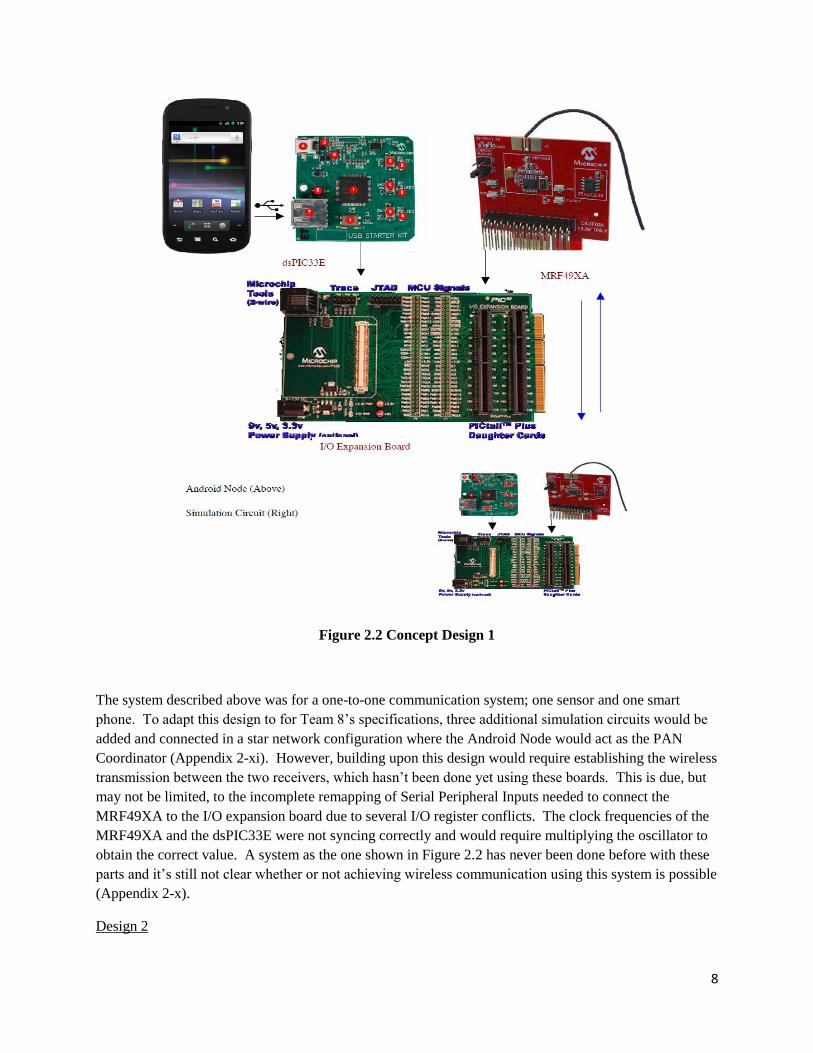
Design 1
When deciding on a design solution, two conceptual designs were considered. The Design Team (Team 4,
„11) from which this project was inherited created a system using MiWi for wireless communication.
This system (Design 1, Figure 2.2) included two nodes each composed of the following: the dsPIC33E
USB starter kit, an I/O expansion board and a MRF49XA wireless transceiver (Appendix 2-x). These
boards were used to create the “Android Node”, the node connected directly to the Android smart-phone
and the “Sensor Node”, also referred to as the “Simulation Circuit” which wirelessly sends the commands
to the Android Node.
8
Figure 2.2 Concept Design 1
The system described above was for a one-to-one communication system; one sensor and one smart
phone. To adapt this design to for Team 8‟s specifications, three additional simulation circuits would be
added and connected in a star network configuration where the Android Node would act as the PAN
Coordinator (Appendix 2-xi). However, building upon this design would require establishing the wireless
transmission between the two receivers, which hasn‟t been done yet using these boards. This is due, but
may not be limited, to the incomplete remapping of Serial Peripheral Inputs needed to connect the
MRF49XA to the I/O expansion board due to several I/O register conflicts. The clock frequencies of the
MRF49XA and the dsPIC33E were not syncing correctly and would require multiplying the oscillator to
obtain the correct value. A system as the one shown in Figure 2.2 has never been done before with these
parts and it‟s still not clear whether or not achieving wireless communication using this system is possible
(Appendix 2-x).
Design 2
9
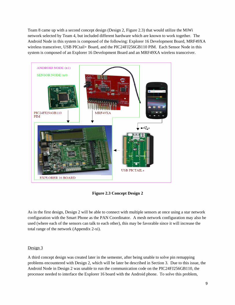
Team 8 came up with a second concept design (Design 2, Figure 2.3) that would utilize the MiWi
network selected by Team 4, but included different hardware which are known to work together. The
Android Node in this system is composed of the following: Explorer 16 Development Board, MRF49XA
wireless transceiver, USB PICtail+ Board, and the PIC24FJ256GB110 PIM. Each Sensor Node in this
system is composed of an Explorer 16 Development Board and an MRF49XA wireless transceiver.
Figure 2.3 Concept Design 2
As in the first design, Design 2 will be able to connect with multiple sensors at once using a star network
configuration with the Smart Phone as the PAN Coordinator. A mesh network configuration may also be
used (where each of the sensors can talk to each other), this may be favorable since it will increase the
total range of the network (Appendix 2-xi).
Design 3
A third concept design was created later in the semester, after being unable to solve pin remapping
problems encountered with Design 2, which will be later be described in Section 3. Due to this issue, the
Android Node in Design 2 was unable to run the communication code on the PIC24FJ256GB110, the
processor needed to interface the Explorer 16 board with the Android phone. To solve this problem,

10
Design 3 changes the design of the Android Node to be composed of two Explorer 16 development
boards instead of one, and therefore 2 different processors. The Android Node will then be composed of
one board which has the wireless communication functionality to transfer data from the sensor nodes and
the other board which has the USB communication functionality to transfer the data to the smart-phone.
These two boards communicate between each other directly by bit manipulation on several pins which we
will be wired together, shown in Figure 2.4. No changes will be made to the sensor nodes, however,
since an extra development board was needed for the Android node, there will be three sensor nodes
instead of four.
Figure 2.4 Design 3 – Android Node
2.4 Feasibility of the Concept Designs
In order to quantify the feasibility of each proposed solution, a Feasibility Matrix was used, Table 2.2.
The Feasibility Matrix does not include Design 3, since Design 3 was introduced as a solution to
problems encountered in Design 2. Four types of feasibility were examined: operational, technical,
scheduling, and economical feasibility. Design 2 was determined to be more feasible in terms of schedule
and technical feasibility.

11
Table 2.2 Feasibility Matrix
In terms of operational feasibility, both designs use a MiWi network in order to communicate between the
smart phone and the sensors. MiWi was chosen before us. It‟s a good choice for wireless communication
because one of the design requirements were not to use any existing infrastructures (such as WiFi or the
cellular network), due to the fact that the locations the sensors will be placed may not be near any of these
pre-existing infrastructures.
For technical feasibility, Design 1 was determined slightly less feasible due to the fact that still there
hasn‟t been a successful attempt to create a MiWi network using the parts listed in the description of
Design 1. For Design 2, it was believed that all parts were compatible with each other. We were using
recommended parts for Android communication with the Explorer 16 and the RF transceivers are
compatible. Last year, Team 4 programmed and proved that wireless communication between two
Explorer 16 Development Boards is very feasible.
As far as scheduling feasibility, Design 1 was at a disadvantage since Team 4 has identified problems that
could not be solved in the amount of time given. For Design 2, there were no foreseen problems to get
the basic design to work. Scheduling and project management is further discussed in Section 2.6.
Economically, Battelle has offered to provide the parts needed to complete the project. The budget will
be significantly more than last years since we‟re going to create a network using 4 sensors and test them
simultaneously.
2.5 Project Management and Schedule
Proper project management is in place to ensure project completion by the fixed due date, Design Day.
The Gantt Chart for our project is shown in Figure 2.5. We broke the job into seven main sections.
“Project Definition” and “Developing Conceptual Design” tasks were to be completed by the entire group
within the first two weeks of the assigned project. The development of the Android GUI code (Paul and
Micah), the code for both nodes and the MiWi communication code (Hun, Steve, and Michael) was to be
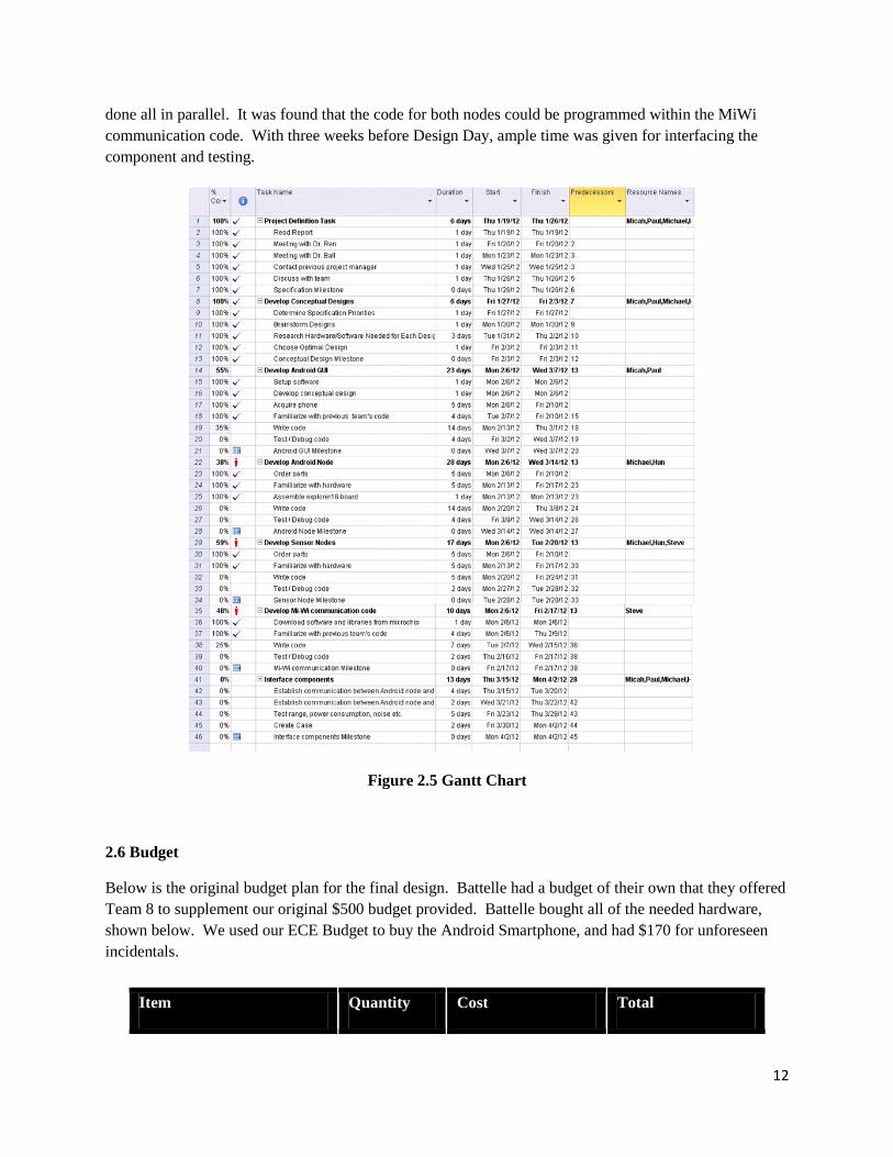
12
done all in parallel. It was found that the code for both nodes could be programmed within the MiWi
communication code. With three weeks before Design Day, ample time was given for interfacing the
component and testing.
Figure 2.5 Gantt Chart
2.6 Budget
Below is the original budget plan for the final design. Battelle had a budget of their own that they offered
Team 8 to supplement our original $500 budget provided. Battelle bought all of the needed hardware,
shown below. We used our ECE Budget to buy the Android Smartphone, and had $170 for unforeseen
incidentals.
Item Quantity Cost Total
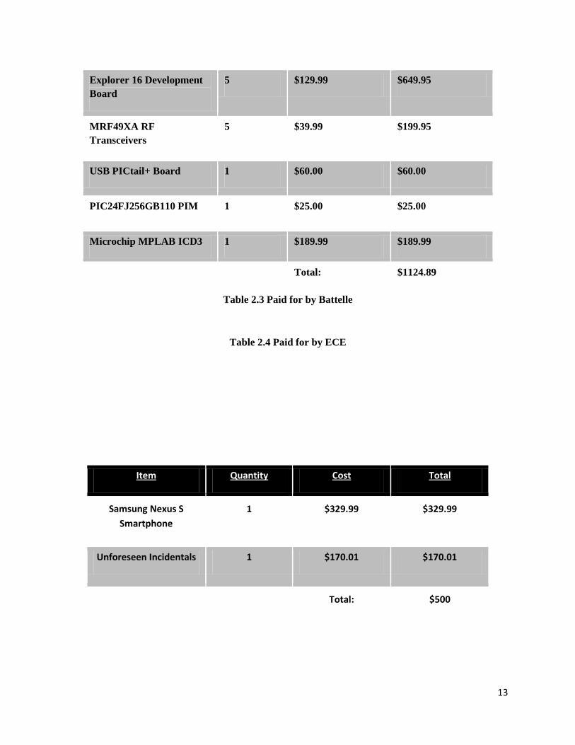
13
Table 2.3 Paid for by Battelle
Table 2.4 Paid for by ECE
Explorer 16 Development
Board
5 $129.99 $649.95
MRF49XA RF
Transceivers
5 $39.99 $199.95
USB PICtail+ Board 1 $60.00 $60.00
PIC24FJ256GB110 PIM 1 $25.00 $25.00
Microchip MPLAB ICD3 1 $189.99 $189.99
Total: $1124.89
Item Quantity Cost Total
Samsung Nexus S
Smartphone
1 $329.99 $329.99
Unforeseen Incidentals 1 $170.01 $170.01
Total: $500
14
Chapter 3:Technical Description of Work Performed
Team 8 considered three design proposals (outlined in Section 2.3), each requiring different
hardware and software configurations. Chapter 3 will discuss in detail the configurations and
technical work performed for both Design 2 and the Design 3 (the final design). Design 2 is
composed of an Android node and 4 sensor simulator nodes. Design 3, on the other hand,
involves an Android node 1, Android node 2, and 3 sensor simulator nodes. The following is a
description of the hardware components used in both designs.
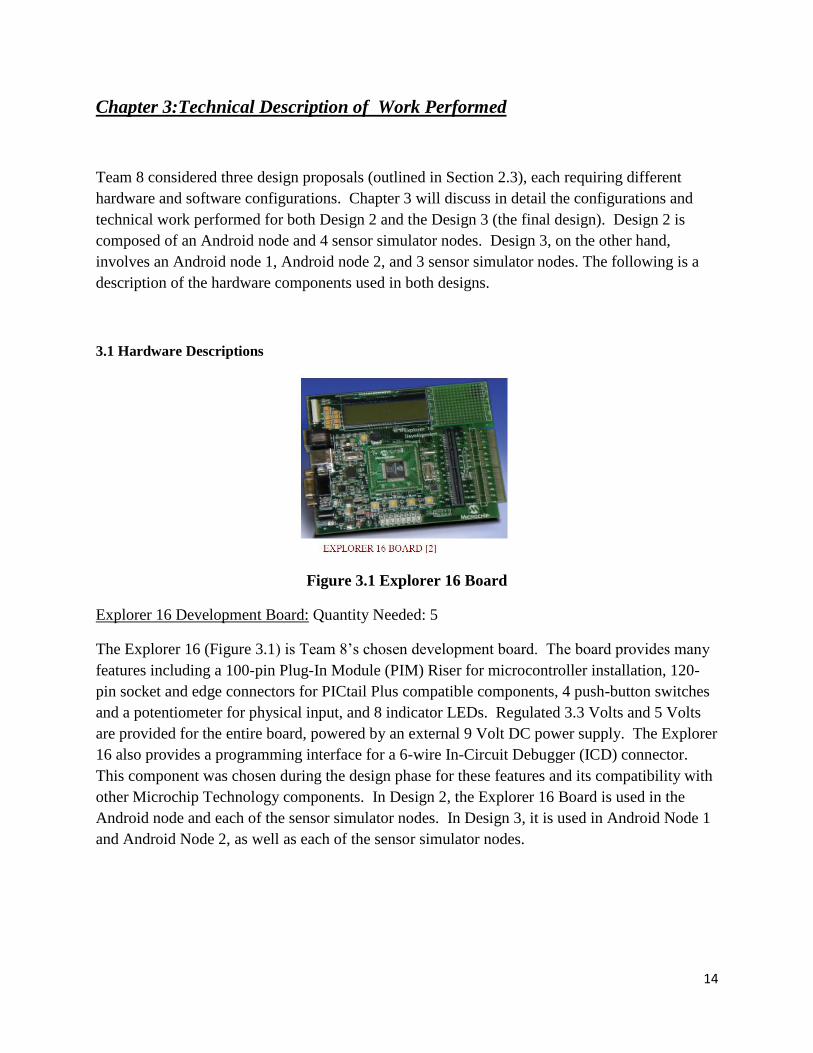
3.1 Hardware Descriptions
Figure 3.1 Explorer 16 Board
Explorer 16 Development Board: Quantity Needed: 5
The Explorer 16 (Figure 3.1) is Team 8‟s chosen development board. The board provides many
features including a 100-pin Plug-In Module (PIM) Riser for microcontroller installation, 120-
pin socket and edge connectors for PICtail Plus compatible components, 4 push-button switches
and a potentiometer for physical input, and 8 indicator LEDs. Regulated 3.3 Volts and 5 Volts
are provided for the entire board, powered by an external 9 Volt DC power supply. The Explorer
16 also provides a programming interface for a 6-wire In-Circuit Debugger (ICD) connector.
This component was chosen during the design phase for these features and its compatibility with
other Microchip Technology components. In Design 2, the Explorer 16 Board is used in the
Android node and each of the sensor simulator nodes. In Design 3, it is used in Android Node 1
and Android Node 2, as well as each of the sensor simulator nodes.

15
Figure 3.2 MRF49XA
MRF49XA PICtail / PICtail Plus Daughter Board: Quantity Needed: 5
The MRF49XA (Figure 7) is a Sub-GHz RF transceiver, with a 300 meter range. The daughter
board it is installed on provides 2 kB EEPROM, a 30-pin edge connector to interface with the
Explorer 16 Development Board and a 3.3 inch wire antenna for optimal data transmission. This
component was chosen for its ability to interface with the Explorer 16 and its compatibility with
Microchip Technology‟s MiWi wireless protocol. In Design 2, this is used in the Android node
and each of the sensor simulator nodes. In the Design 3, one MRF49XA transceiver is connected
to the Android Node 2, as well as one for each of the sensor simulator nodes.
Figure 3.3 USB PICTAIL+
USB PICtail Plus Daughter Board: Quantity Needed: 1
The USB PICtail Plus daughter board is a 120-pin demonstration board designed for use with the
Explorer 16 Development board. It contains a USB port and a 120-pin PICtail Plus edge
connector. This component was chosen to allow transfer of data between an Android
smartphone and the Explorer 16 board. It is used in the Android node in Design 2 and in
Android node 1 in Design 3.

16
Figure 3.4 PIC24FJ256GB110
PIC24FJ256GB110 Microcontroller: Quantity Needed: 1
Team 8 chose Microchip Technology‟s 100-pin PIC24FJ256GB110 as the Android node
microcontroller in Design 2, and as the Android 1 node microcontroller in Design 3. It is a 16-
Bit flash microcontroller with USB v2.0 capabilities. Also featured in this model is a peripheral
pin select feature, allowing the user to reassign pin functionality as needed. The ability to remap
a large number of peripheral pins was a critical factor in Team 8‟s decision to use this
microcontroller. It was believed one of the main reasons for the previous design team‟s inability
to establish wireless communication was due to pin remapping issues. This, along with the
PIC24FJ256GB110 microcontroller‟s USB communication capabilities made Team 8 chose this
component.
Figure 3.5 PIC24FJ128GA010
PIC24FJ128GA010 Microcontroller: Quantity Needed: 4
The 100-pin PIC24FJ128GA010 microcontroller was selected for use in the sensor simulator
nodes for Design 2, and the Android Node 2 as well as each of the sensor nodes for Design 3.
Like the PIC24FJ256GB110, this is a 16-Bit flash microcontroller. Unlike the former, this
microcontroller has neither USB capability nor peripheral pin select features. However, these
features are unnecessary in Team 8‟s final design; no remapping is required to interface the
transceivers to these boards and no USB communication is involved.

17
3.2 Design 2 Hardware Configuration
Design 2 was the initial design solution of Team 8. The team later decided upon an alternative
design solution (Design 3) which will be discussed in later sections. A detailed description of
hardware setup, configuration, and installation is for Design 2 is provided.
Sensor Simulator Nodes
Team 8 chose to simulate remote sensors using three components; the PIC24FJ128GA010
microcontroller (Appendix 3 - figure 2), the Explorer 16 development board (Appendix 3 –
figure 11), and the MRF49XA wireless transceiver (Appendix 3 – figure 9). Each of these
components are created and sold by Microchip Technology.
To assemble these components, Team 8 first installed the microcontroller onto the 100-pin PIM
riser on the development board. The wireless transceiver was then installed onto the
development board via the PICtail Plus socket. Lastly, connecting a 9 Volt DC power supply to
the development board‟s power input completed the hardware assembly of the sensor simulator.
Android Node
The interface for the smartphone is comprised of the PIC24FJ256GB110 microcontroller
(Appendix 3 – Figure 7), the Explorer 16 development board, the USB PICtail Plus daughter
board (Appendix 3 – Figure 6), and a 120-pin socket.
Assembling these components required installing the microcontroller onto the 100-pin PIM riser,
connecting the USB PICtail Plus daughter board to the development board‟s PICtail Plus edge
connector, connecting the 120-pin socket to the PICtail Plus edge connector of the USB daughter
board. This node also requires a 9 Volt DC power supply connected to the board‟s power input.
3.3 Design (2) Software Development
Team 8 downloaded free demonstration code from Microchip Technology‟s website (Appendix
2-v) which is the basis for most of Design 2‟s software development. The software development

18
and modification for Design 2 can be described in 3 sub-sections; sensor simulator node code,
Android node code, and Android phone application code.
Sensor Simulator Node Code
The code for the sensor simulator nodes was never fully implemented for Design 2 due to issues
with the Android node code in this design. However, the code for Design 2 would have been
implemented in a similar way to how it was implemented in the final design. See Design 3
(Section 3.4) for a description of the software implementation.
Android Node Code
The Android node code for Design 2 was intended to implement 3 functionalities;
communication with the Android smartphone via USB, sending data to the sensor simulator
nodes, and receiving data from the sensor simulator nodes.
Team 8 used Microchip Technology‟s Android firmware code examples provided on their
website (Appendix 2) for most of the USB communication. After programing the
PIC24FJ256GB110 microcontroller on the Android node, communication was possible between
various parts of the Explorer 16 board and the Android smartphone. Displaying button presses
on the phone was accomplished by first defining the following functions in “HardwareProfile.h”,
a configuration file.
Figure 3.6 Button Press Code
It was then necessary to send data to the phone through USB whenever a button was pressed.
The function GetPushbuttons() accomplishes this. The variable toReturn is the byte value sent to
the smartphone.
#define Switch1Pressed() ((PORTAbits.RA10 == 1)? TRUE : FALSE)
#define Switch2Pressed() ((PORTAbits.RA2 == 1)? TRUE : FALSE)
#define Switch3Pressed() ((PORTAbits.RA3 == 1)? TRUE : FALSE)
#define Switch4Pressed() ((PORTDbits.RD6 == 1)? TRUE : FALSE)

19
Figure 3.7 GetPushButton Code
The potentiometer values were also sent to the phone when the potentiometer‟s status changed.
Whenever tempValue has changed, the potentiometer is read again and the data is later sent to
the smartphone.
Figure 3.8 Reading Potentiometer Code
This code provided by Microchip Technology worked fine for the PIC24FJ256GB110 and the
Explorer 16. Team 8 now attempted to integrate this code with Microchip‟s example code for
sending and receiving data via the MiWi protocol. It was here that the team ran into major issues.
static BYTE GetPushbuttons(void)
{
BYTE toReturn;
InitAllSwitches();
toReturn = 0;
if(Switch1Pressed()){toReturn |= 0x1;}
if(Switch2Pressed()){toReturn |= 0x2;}
if(Switch3Pressed()){toReturn |= 0x4;}
if(Switch4Pressed()){toReturn |= 0x8;}
return toReturn;
}
//Get the current potentiometer setting
tempValue = ReadPOT();
//If it is different than the last time we read the pot, then we need
// to send it to the Android device
if(tempValue != potPercentage)
{ potNeedsUpdate = TRUE;
potPercentage = tempValue; }

20
Microchip‟s demonstration code for basic MiWi communication assumes the use of the
PIC24FJ128GA010 microcontroller. It also provides support for several other microcontrollers,
but none of these include the PIC24FJ256GB110 microcontroller that Team 8 was attempting to
use. Many of the pins required for the serial peripheral interface (SPI) in the example code were
already in use by this specific microcontroller for use in the USB Android communication code.
When choosing this design, Team 8 believed the choice of hardware would avoid this problem,
but this was not the case.
To fix this issue, Team 8 researched the PIC24FJ256GB110 peripheral pin selection features
(Appendix 2) . It was believed that the following code would remap the necessary pins to
integrate the MiWi communication code with the USB Android communication code. These are
the pins used for SPI communication with the MRF49XA transceivers in the MiWi
communication code.
Figure 3.9 Peripheral Pin Select
However, these changes were unhelpful in integrating the code. After many attempts and
approaches to solving this issue and many phone calls and emails to Microchip Technology to no
avail, Team 8 decided on a different solution for the design. In the interest of time Team 8
decided to implement Design 3, an approach described in the next section. This approach
//-----Unlocks PPS------
__builtin_write_OSCCONL(OSCCON & 0xBF);
//--------INPUTS--------
//assign INT4 to pin RPI35
RPINR2bits.INT4R = 35;
//assign INT3 to pin RPI36
RPINR1bits.INT3R = 36;
//assign SDI2 to pin RP26
RPINR22bits.SDI2R = 26;
//assign U2CTS to pin RPI32
RPINR19bits.U2CTSR = 32;
//assign U2RX to pin RP10
RPINR19bits.U2RXR = 10;
////-------OUTPUTS-------
//assign SCK2 to pin RP21
RPOR10bits.RP21R = 11;
//assign SS2 to pin RP27
RPOR13bits.RP27R= 12;
//assign U2RTS to pin RP31
RPOR15bits.RP31R= 6;
//assign U2TX to pin RP17
RPOR8bits.RP17R = 5;
//-----_Locks PPS------
__builtin_write_OSCCONL(OSCCON | 0x40);

21
eliminates the need to remap pins by using 2 nodes with different microcontrollers to implement
the Android node.
Android Phone Application Code
The code for the Android phone application was never fully implemented for Design 2 due to
issues with the Android node code in this design. However, the code for Design 2 would have
been implemented in a similar way to how it was implemented in the final design. See Design 3
(Section 3.5 Android Phone Application Code) for a description of the software implementation.
3.4 Design 3 Hardware Configuration and Implementation
Design 3 avoids the issues described in Design 2 (section 3.2 Android Node Code) by splitting
the Android node into 2 separate nodes. The description of the hardware design for Design 3 can
be divided into four subsections; the sensor simulator nodes, the central wireless connection node
(Android node 2), the smartphone interface (Android node 1), and the enclosure. A detailed
description of hardware setup, configuration, and installation is for Design 3 is provided.
Simulation Sensor Nodes
The sensor simulation node hardware for Design 3 was implemented the same as Design 2. See
Design 2 sensor simulator nodes for the detailed configuration.
Android Node 2 – Central Wireless Communication Node
Android node 2 was implemented to correct for peripheral pin selection issues in Design 2. The
sensor nodes communicate directly with Android node 2 which then sends the received data to
Android node 1. This node is similar to the sensor simulator nodes. There are three major
hardware components; the PIC24FJ128GA010 microcontroller, the Explorer 16 development
board, and the MRF49XA wireless transceiver. These are installed in the same way as the sensor
simulator nodes. However, this node also has a 120-pin socket connected to the development
board‟s PICtail Plus edge connector. Eight wires were soldered to the 120-pin socket for
communication with the Android node 1 board (pin selection and configuration is discussed in
section 3.5).
22
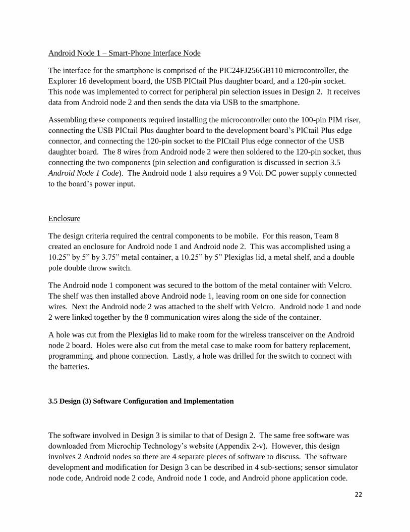
Android Node 1 – Smart-Phone Interface Node
The interface for the smartphone is comprised of the PIC24FJ256GB110 microcontroller, the
Explorer 16 development board, the USB PICtail Plus daughter board, and a 120-pin socket.
This node was implemented to correct for peripheral pin selection issues in Design 2. It receives
data from Android node 2 and then sends the data via USB to the smartphone.
Assembling these components required installing the microcontroller onto the 100-pin PIM riser,
connecting the USB PICtail Plus daughter board to the development board‟s PICtail Plus edge
connector, and connecting the 120-pin socket to the PICtail Plus edge connector of the USB
daughter board. The 8 wires from Android node 2 were then soldered to the 120-pin socket, thus
connecting the two components (pin selection and configuration is discussed in section 3.5
Android Node 1 Code). The Android node 1 also requires a 9 Volt DC power supply connected
to the board‟s power input.
Enclosure
The design criteria required the central components to be mobile. For this reason, Team 8
created an enclosure for Android node 1 and Android node 2. This was accomplished using a
10.25” by 5” by 3.75” metal container, a 10.25” by 5” Plexiglas lid, a metal shelf, and a double
pole double throw switch.
The Android node 1 component was secured to the bottom of the metal container with Velcro.
The shelf was then installed above Android node 1, leaving room on one side for connection
wires. Next the Android node 2 was attached to the shelf with Velcro. Android node 1 and node
2 were linked together by the 8 communication wires along the side of the container.
A hole was cut from the Plexiglas lid to make room for the wireless transceiver on the Android
node 2 board. Holes were also cut from the metal case to make room for battery replacement,
programming, and phone connection. Lastly, a hole was drilled for the switch to connect with
the batteries.
3.5 Design (3) Software Configuration and Implementation
The software involved in Design 3 is similar to that of Design 2. The same free software was
downloaded from Microchip Technology‟s website (Appendix 2-v). However, this design
involves 2 Android nodes so there are 4 separate pieces of software to discuss. The software
development and modification for Design 3 can be described in 4 sub-sections; sensor simulator
node code, Android node 2 code, Android node 1 code, and Android phone application code.
23
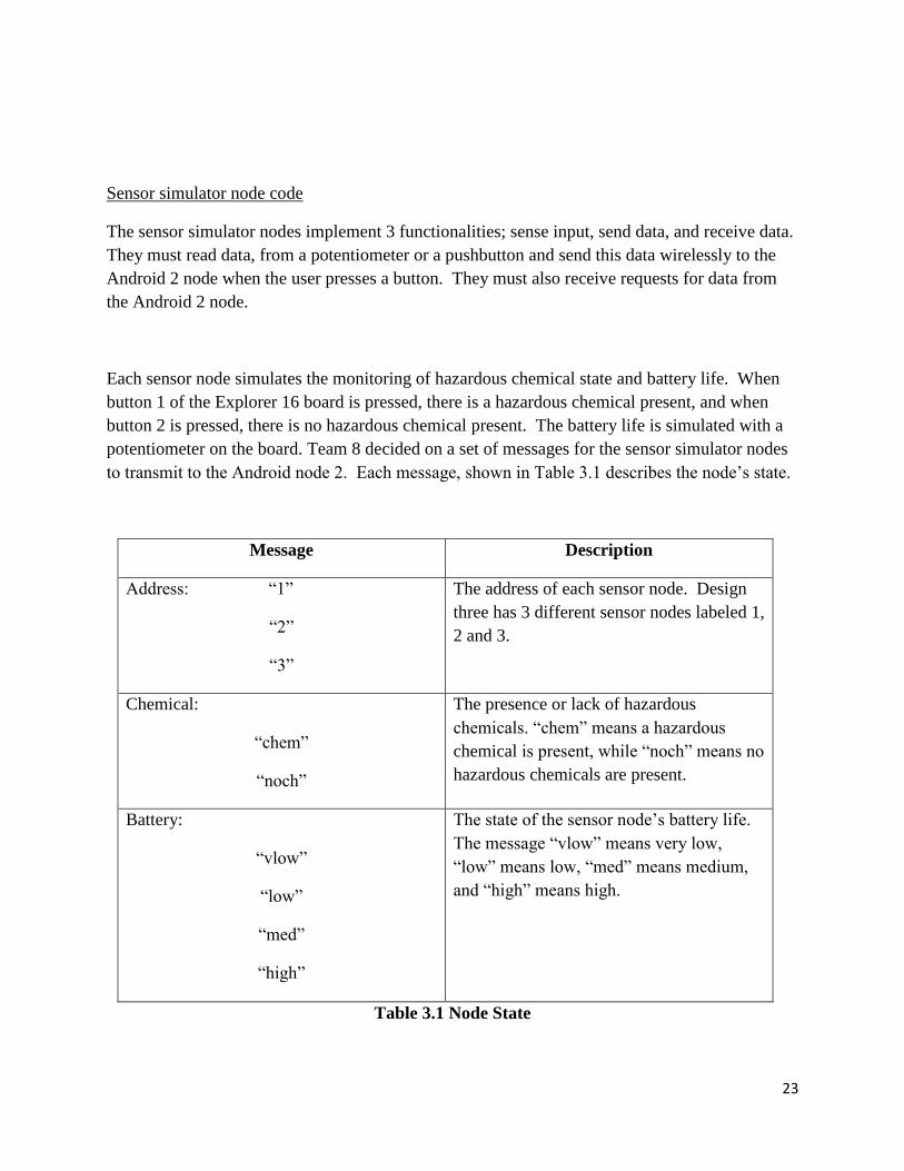
Sensor simulator node code
The sensor simulator nodes implement 3 functionalities; sense input, send data, and receive data.
They must read data, from a potentiometer or a pushbutton and send this data wirelessly to the
Android 2 node when the user presses a button. They must also receive requests for data from
the Android 2 node.
Each sensor node simulates the monitoring of hazardous chemical state and battery life. When
button 1 of the Explorer 16 board is pressed, there is a hazardous chemical present, and when
button 2 is pressed, there is no hazardous chemical present. The battery life is simulated with a
potentiometer on the board. Team 8 decided on a set of messages for the sensor simulator nodes
to transmit to the Android node 2. Each message, shown in Table 3.1 describes the node‟s state.
Message Description
Address: “1”
“2”
“3”
The address of each sensor node. Design
three has 3 different sensor nodes labeled 1,
2 and 3.
Chemical:
“chem”
“noch”
The presence or lack of hazardous
chemicals. “chem” means a hazardous
chemical is present, while “noch” means no
hazardous chemicals are present.
Battery:
“vlow”
“low”
“med”
“high”
The state of the sensor node‟s battery life.
The message “vlow” means very low,
“low” means low, “med” means medium,
and “high” means high.
Table 3.1 Node State

24
Each sensor node also responds to a connection request sent from the Android node 2. Upon
receiving this request the sensor simulator node transmits its state once more. This is useful for
the Android node 2 in determining whether a connection has timed out.
Android Node 2 Code
The Android node 2 is necessary in Design 3 for communication with Android node 1. This
eliminates the need to remap peripherals as in Design 2. It implements three different
functionalities; receive data, send data, and communicate with the Android node 1. It must
receive messages from the sensor simulator nodes when they each send their state information,
and must send data request back to the sensors upon connection timeout. It must also send data
to the Android 1 node via the 8 peripheral pins that connect them.
The messages received from the sensor simulator nodes can be viewed in Table 3.1. If a node
has not communicated with the Android node 2 for a certain amount of time, a data request must
be sent. This was implemented using a timeout loop of 30 seconds after which a data request is
sent to each sensor. Upon receiving data from a sensor simulator node, the Android node 2
sends the data to Android node 1 using 8 bits. Each bit represents the data sent from a sensor
and can be seen in Table 3.2.
Bit Number Functionality
7 1 indicates a message has been sent. 0
indicates no message has been sent.
6, 5 Address of the sending sensor node.
01 indicates node “1”
10 indicates node “2”
11 indicates node “3”
4 1 indicates hazardous chemical present
0 indicates no hazardous chemical present
3, 2 Battery life of the sensor node.
00 indicates very low
01 indicates low
10 indicates medium

25
11 indicates high
1, 0 Address of any disconnected sensor node.
01 indicates node “1”
10 indicates node “2”
11 indicates node “3”
Table 3.2 Bit Functionality
These bits are immediately sent to Android node 1 for communication with the Android
smartphone.
Android Node 1 Code
The implementation of the Android node 1 code is similar to that of Design 2. However one key
difference between the two implementations is that in this design, the node reads peripheral bits
rather than buttons. The bit assignment has been changed so the buttons no longer control the
SwitchXPressed() function but rather the peripheral pins. The code in Figure 3.6 is now changed
to the following.
Figure 3.10 Button Press Code
#define Switch1Pressed() ((PORTAbits.RA2 == 1)? TRUE : FALSE)
#define Switch2Pressed() ((PORTAbits.RA3 == 1)? TRUE : FALSE)
#define Switch3Pressed() ((PORTAbits.RA10 == 1)? TRUE : FALSE)
#define Switch4Pressed() ((PORTDbits.RA1 == 1)? TRUE : FALSE)
#define Switch5Pressed() ((PORTAbits.RA5 == 1)? TRUE : FALSE)
#define Switch6Pressed() ((PORTAbits.RA7 == 1)? TRUE : FALSE)
#define Switch7Pressed() ((PORTAbits.RD7 == 1)? TRUE : FALSE)
#define Switch8Pressed() ((PORTDbits.RD6 == 1)? TRUE : FALSE)

26
Similarly the code in Figure 3.7 is also now modified to send 4 more bytes to the Android smart
phone in the following manner.
Figure 3.11 GetPushButton Code
The rest of the Android node 1 code is nearly the same as in Design 2
Android Phone Application Code
The Android application code was based on Microchip Technology‟s Basic Accessory Demo.
Team 8 modified it to implement the functionality of displaying information sent by Android
node 1. The application waits for a data transfer from the USB connection with Android node 1
and updates several displays representing the sensor simulator nodes.
static BYTE GetPushbuttons(void)
{
BYTE toReturn;
InitAllSwitches();
toReturn = 0;
if(Switch1Pressed()){toReturn |= 0x1;}
if(Switch2Pressed()){toReturn |= 0x2;}
if(Switch3Pressed()){toReturn |= 0x4;}
if(Switch4Pressed()){toReturn |= 0x8;}
if(Switch1Pressed()){toReturn |= 0x10;}
if(Switch2Pressed()){toReturn |= 0x20;}
if(Switch3Pressed()){toReturn |= 0x40;}
if(Switch4Pressed()){toReturn |= 0x80;}

27
This excerpt of android code shows how we implemented the displaying of the information
received from the sensor nodes.
Figure 3.12 updateNodes Code
private void updateNodes(){ if (address == 1 && connected==0){ ib1.setImageResource(R.drawable.greenconnected); if (chem == 1){ b1.setImageResource(R.drawable.danger); } else{ b1.setImageResource(R.drawable.safe); } switch(battery){ case 0: p1.setProgress(0); break; case 1: p1.setProgress(15); break; case 2: p1.setProgress(50); break; case 3: p1.setProgress(100); break; } } if (connected==1){ ib1.setImageResource(R.drawable.redconnected); b1.setImageResource(R.drawable.safe); p1.setProgress(0); } }
28
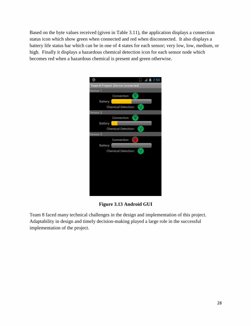
Based on the byte values received (given in Table 3.11), the application displays a connection
status icon which show green when connected and red when disconnected. It also displays a
battery life status bar which can be in one of 4 states for each sensor; very low, low, medium, or
high. Finally it displays a hazardous chemical detection icon for each sensor node which
becomes red when a hazardous chemical is present and green otherwise.
Figure 3.13 Android GUI
Team 8 faced many technical challenges in the design and implementation of this project.
Adaptability in design and timely decision-making played a large role in the successful
implementation of the project.
29
Chapter 4 – Test Data with Proof of Functional Design
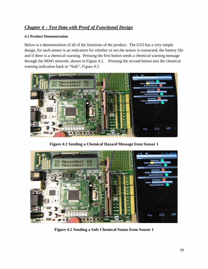
4.1 Product Demonstration
Below is a demonstration of all of the functions of the product. The GUI has a very simple
design, for each sensor is an indication for whether or not the sensor is connected, the battery life
and if there is a chemical warning. Pressing the first button sends a chemical warning message
through the MiWi network, shown in Figure 4.1. Pressing the second button sets the chemical
warning indication back to “Safe”, Figure 4.2.
Figure 4.1 Sending a Chemical Hazard Message from Sensor 1
Figure 4.2 Sending a Safe Chemical Status from Sensor 1
30
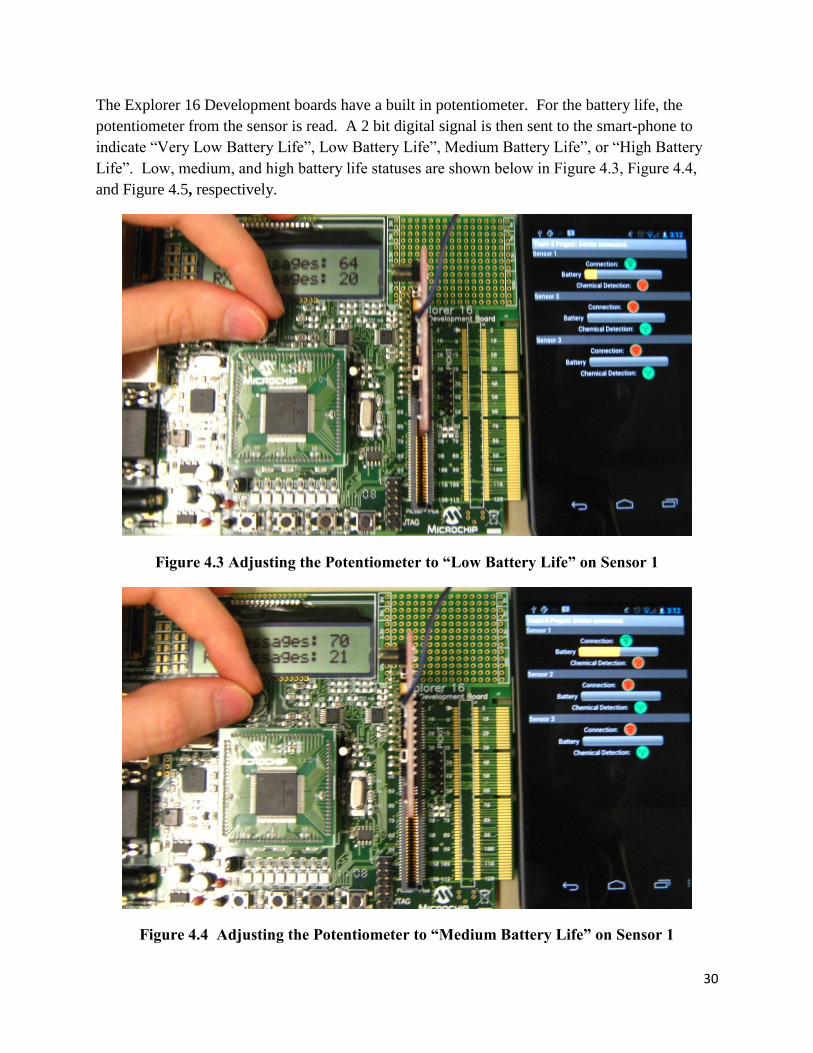
The Explorer 16 Development boards have a built in potentiometer. For the battery life, the
potentiometer from the sensor is read. A 2 bit digital signal is then sent to the smart-phone to
indicate “Very Low Battery Life”, Low Battery Life”, Medium Battery Life”, or “High Battery
Life”. Low, medium, and high battery life statuses are shown below in Figure 4.3, Figure 4.4,
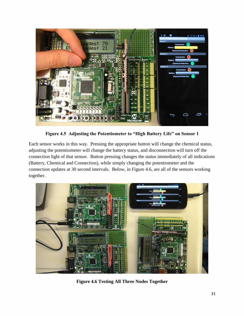
and Figure 4.5, respectively.
Figure 4.3 Adjusting the Potentiometer to “Low Battery Life” on Sensor 1
Figure 4.4 Adjusting the Potentiometer to “Medium Battery Life” on Sensor 1
31
Figure 4.5 Adjusting the Potentiometer to “High Battery Life” on Sensor 1
Each sensor works in this way. Pressing the appropriate button will change the chemical status,
adjusting the potentiometer will change the battery status, and disconnection will turn off the
connection light of that sensor. Button pressing changes the status immediately of all indications
(Battery, Chemical and Connection), while simply changing the potentiometer and the
connection updates at 30 second intervals. Below, in Figure 4.6, are all of the sensors working
together.
Figure 4.6 Testing All Three Nodes Together

32
4.2 Data Refresh Testing
As stated in Section 4.1, button pressing changes the status of the sensor immediately. To keep
track of the potentiometer and the connection status when a message isn‟t being sent, the
Android node sends out a request to all of the nodes to send their states. Originally, after sending
a chemical change from one sensor, that sensor‟s chemical status would correctly change, but
then at the 30 second update, all of the sensors would be updated with the most recent change.
This was fixed by storing the correct state within each sensor.
Testing has been done to be sure that the connection status and the battery status is always
registered. This is done by disconnecting all of the sensor nodes in every order. We found a
problem when disconnecting the nodes from the highest node to the lowest node, due to the order
of our if-statements. A delay loop between each if-statement was required to remedy this.
4.3 Simultaneous Message Testing
To ensure that messages could be sent simultaneously, messages were sent at the same time to
make sure the change was registered on the GUI. One person pressed the send button from all of
the sensor nodes near-simultaneously (all within one-half of a second of each other), alternating
between sending “Hazardous Chemical” and “No Hazardous Chemical” messages. Out of 100
messages from each node, all 300 messages were registered on the GUI.
4.4 MiWi Range Testing
To test the range of the MiWi network, we used Microchip‟s “Simple Example” code provided
in the Microchip Application Library. This code displays on the LCD screen the number of
messages transmitted and received. The space was limited to the size of the hallways in the
Engineering Building. The sensor nodes communicate with the central node via unicasting; the
indoor unicasting results are shown in Figure 4.7.
Figure 4.7 Indoor Range Testing
0
20
40
60
80
100
50 100 150 200 250 300 350 400 450
%
R
e
c
e
i
v
e
d
Distance (ft)
Indoor Unicast Testing
Empty Hall - Test 1
Empty Hall - Test 2
Full Hall - Test 3
Full Hall - Test 4

33
As you can see from Figure 4.7, we tested sending in both an empty hall (at night), and a full hall
(during the day), the results showed that the number of messages received decreased as the
number of people in the hall increased. During each test, 25 messages were sent every 50 feet.
In Test 1, every message was received. In Test 2, a total of 2 messages were dropped out of the
225 total messages sent. In the full halls, the number of messages received were based more on
the number of people in the hallway, than the distance distance between the transcievers.
Based on the results above, it was decided that testing should be done with sending messages
around an obstacle. The results of these tests are shown in Figure 4.8. In these tests, each
transciever was moved 25 feet from the intersection of the hallway, increasing the hypotenuse by
about 35 feet between every transmission. The number of transmissions in each test were 25, just
as above. This shows that there was a dramatic decrease of message, in both tests after each
transciever was 225 feet away from the center, with a hypotenuse of about 318 feet. There is a
general trend of decreasing messages as the obstacle between the two transceivers increased.
Figure 4.8 Indoor Range Testing Around Obstacle
Outdoor testing allows us to test the full range of the system. Outdoor testing was done just as
the indoor tests, 25 messages were sent every 50 feet. The results of the outdoor testing are
shown in Figure 4.9. In both tests, there was a drop rate of less than 20% up to 500 feet. In Test
1, we see a general decline as the distance increases. In Test 2, however, we see a drop rate of
less than 25% up to 1000 feet. At 1100 feet, only one message was dropped. These results show
that the MiWi network can extend to the expected range of 300 meters.
0102030405060708090
100
35
.35
70
.7
10
6.0
5
14
1.4
17
6.7
5
21
2.1
24
7.4
5
28
2.8
31
8.1
5
35
3.5
38
8.8
5
%
R
e
c
e
i
v
e
d
Distance (ft)
Indoor Unicast Testing Around Corner
Empty Hall - Test 1
Empty Hall - Test 2

34
Our simulation circuits are programmed to send just one message when a button is pressed.
However, in actual applications, the sensors will be constantly updating the central node with
their status. Even a high drop rate will provide adequate data to the central node.
Figure 4.9 Outdoor Range Testing

35
Chapter 5 – Final cost, schedule, summary and conclusions
5.1 Findings
Evaluating the final product versus the design specifications it is easy to see the success obtained
in our design. The goal of the design is achieve wireless communication with multiple sensors
and to display the results of that communication on a graphical user interface (GUI). As seen
from the report the main success of the design is the implementation of the wireless
communication not achieved by the previous group. Although the prototype could have been
smaller and more adaptable, it does give a functional demonstration of how an Android based
smartphone in conjunction with accessory hardware can reliably communicate with various
sensors via a wireless network.
With that said, the simplicity of the final design did not come without its fair amount of trials.
Most notably was the attempt to integrate the USB and wireless functionality onto the same
microcontroller. We attempted many solutions as seen in chapter 3 and eventually settled on our
current solution. It is the opinion of this team however, that this design can be achieved using
only one micro controller. This would take much more time and effort than the time allotted for
this design and is therefore not feasible for this team.
When it was decided that this was not a possibility, our current design was implemented. This
design both meets the requirements of the sponsor and decreases the time to implement the final
product allowing for completion by the designated date. The success of the design displays the
capability of such a device and makes this prototype invaluable in the development of a finalized
product should that be desired.
5.2 Suggestions for future projects
The two main suggestions this team has for future works are to integrate the USB and wireless
functionality onto a single microcontroller and to eliminate the excess hardware associated with
our prototype.
As stated in our findings, it is believed that integration is entirely possible. The team found that
several pins that were used in wireless communication on the one microcontroller were taken up
by USB functionality on the other controller. The solution to this would be for a future project to
become very knowledgeable on the various pin layouts of the microcontrollers. This would
allow them to successfully remap the pins used in wireless communication to fit beside the pins
used for USB functionality.

36
The suggestion to reduce excess hardware comes from the fact that the development boards were
chosen for the ease of implementation the allowed, not that they were space efficient. The
boards contain a lot of hardware and capabilities that just simply aren‟t being used. In future
projects a smaller less capable board to house the microcontroller could be used without harming
the functionality. As stated above, combining the functionality of the two chips connected to the
phone would also drastically reduce excess hardware.
5.3 Final Cost
The final cost of the project is detailed in the following chart:
Table 5.1 Final Cost
Very generously, our sponsor, Dr. Christopher Ball and his company, Battelle Laboratories,
offered to contribute $1,124.89. This allowed us to stay inside the $500 budget for this project.
Total cost after Battelle‟s contribution = $354.99
5.4 Conclusion
What Worked
The design accomplished the goal of communicating with multiple sensors using an Android
based smartphone. Using various buttons to represent changes the simulated sensor might
experience the data is sent over the wireless network and the data is sent up to the phone and
displayed on the GUI.
What Did Not Work
The goal of getting the wireless and USB capabilities into the same microcontroller was not
accomplished. This team believes, that with more time to obtain the knowledge needed to remap
the pins used in wireless functionality, this task could be accomplished as well.
Item Quantity Cost Total
Explorer 16 Development Board 5 129.99$ 649.95$
MRF49XA RF Tranceiver 5 39.99$ 199.95$
USB PICtail+ Board 1 60.00$ 60.00$
PIC24FJ256GB110 PIM 2 25.00$ 50.00$
Microchip MPLAB ICD3 1 189.99$ 189.99$
Samsung Nexus S 1 329.99$ 329.99$
Total 1,479.88$
37
Summary
The task assigned by Battelle Laboratories was successfully implemented in the prototype. The
sensors are able to communicate data which is received by the phone accessory and displayed on
the phone in an easy to read graphical user interface.
Final Thoughts
With the completion of this prototype, Team 8 is proud to unveil their Android-based wireless
communication sensor interrogator.

38
Appendix 1 – Technical roles, responsibilities, and work accomplished
Stephen Hilton – Team Manager
In the beginning of the semester, Stephen, along with the rest of the team
took part in the research required to determine the appropriate hardware
needed for the final product. He downloaded the MiWi communication
code and configured it from P2P communication for the code to work
properly on the boards. He was in charge of extensive testing on range,
drop-rates, and simultaneous message sending. He did a lot of work with
Michael and Donghun attempting to solve the pin remapping problem.
Debugging of the many variations of pin remapping was tried including
using the PPS macro, and the code found in Figure 3.9. He was in
constant communication with the technical support team at Microchip, in
attempt to find the solution.
It was Stephen, while working with Michael, that suggested the idea of using two Explorer 16
boards instead of one for the Android Node. He and Michael together tested the potential of this
design concept by testing the ability of bit manipulation on both the Android Node 1 and
Android Node 2. Android Node 2 was tested using the multimeter to read the voltage of pins in
the code that we set to one or zero. We tested Android Node 1 by applying a voltage to certain
pins on the board, to make sure that it registered on the phone.
Stephen, along with the team, helped in the debugging of the final product, by testing different
combinations of commands and making sure that the Android GUI updated correctly, including
the tests for the automatic 30 second updates. He, along with the rest of the team, helped
brainstorm for the algorithms needed for the Android Node 2 and the Sensor Node communicate
with each other properly, and in the end have a properly working communication system
between the smartphone and the sensor nodes.
Michael Allon – Documentation Prep
Michael‟s technical tasks included initial design research, peripheral pin
selection and programming for each of the nodes in the project, secondary
design implementation, testing and analyzing the product, and enclosure
design.
Initially Michael and the team researched and discussed how to implement a
design for the project. They came up with a design with 1 Android node
and 4 sensor simulator nodes. To implement this design Michael researched
the two microcontrollers involved in the design, PIC24FJ256GB110 and
PIC24FJ128GA010, and developed code to implement their functionalities.

39
Problems were encountered with peripheral pin selection in the team‟s initial design; some pins
were not remappable and functionalities could not be changed. This halted progress for the team
for a considerable time. Michael was involved with analyzing this problem by reading
documentation and contacting Microchip Technology (designers of the microcontrollers) , and
attempting to determine a solution. In the interest of time the team chose to implement a
different design to meet the specifications. He and Stephen Hilton came up with a solution with
2 Android nodes instead of 1, and 3 sensor simulator nodes. In this design Michael contributed
to peripheral pin selection as well as the coding for the sending and receiving of messages
between sensor simulator nodes and Android nodes. He helped develop a protocol for sending
sensor node status including address, battery life and chemical hazard detection. Upon
completion of the major aspects of the project Michael aided Donghun Ha and Stephen Hilton
with the testing of the products functionality, including range and transmission tests. He and the
team analyzed the testing results and corrected for errors in the code. Finally, Michael and the
team designed and constructed an enclosure to house the final design.
Micah Zastrow – Webmaster
Throughout the semester Micah worked on a variety of aspects of the
project. Micah‟s primary contribution to the group was the design and
development of the Android application. The first task was becoming
familiarized with the Android development environment. Once he was
familiar with Android development he reviewed the demo code that was
created by Microchip. After reviewing the code, he cut out the parts of the
code that were not going to be used in order to make the application more
efficient. Micah then implemented the required functions that were needed
to control the simulated sensor. He modified the LED control class that
Microchip created to allow the phone to monitor different status that the
sensors were sending. These include connection, battery level, and chemical
detection. Micah also helped interface the android phone with the
PIC24FJ256GB110. He helped collaborate with the other team members to make sure that these
two devices were communicating correctly. This was done by modifying the android node code
and the android application code. Once the communication between the phone and the
PIC24FJ256GB110 was completed, his next task was to create the graphical user interface for
the sensor control application. He then designed the user interface to make sure it met the
requirements from our sponsor. The application that he created was simple and easy to use. He
wanted to program it so that anyone could pick up the phone and know exactly what was
happening, without having to be trained on how to use it. After the interface was complete, he
tested the functionality of the application under a variety of circumstances to make sure it
functioned properly. Finally, Micah also helped test the range of the Mi-Wi protocol. This was
done by having two nodes send communications back and forth to each other, and record if any
packets were lost. We would increase the range in increments of fifty feet until we lost
connection.
40
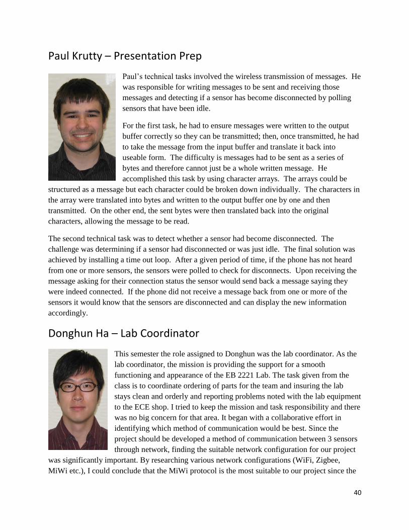
Paul Krutty – Presentation Prep
Paul‟s technical tasks involved the wireless transmission of messages. He
was responsible for writing messages to be sent and receiving those
messages and detecting if a sensor has become disconnected by polling
sensors that have been idle.
For the first task, he had to ensure messages were written to the output
buffer correctly so they can be transmitted; then, once transmitted, he had
to take the message from the input buffer and translate it back into
useable form. The difficulty is messages had to be sent as a series of
bytes and therefore cannot just be a whole written message. He
accomplished this task by using character arrays. The arrays could be
structured as a message but each character could be broken down individually. The characters in
the array were translated into bytes and written to the output buffer one by one and then
transmitted. On the other end, the sent bytes were then translated back into the original
characters, allowing the message to be read.
The second technical task was to detect whether a sensor had become disconnected. The
challenge was determining if a sensor had disconnected or was just idle. The final solution was
achieved by installing a time out loop. After a given period of time, if the phone has not heard
from one or more sensors, the sensors were polled to check for disconnects. Upon receiving the
message asking for their connection status the sensor would send back a message saying they
were indeed connected. If the phone did not receive a message back from one or more of the
sensors it would know that the sensors are disconnected and can display the new information
accordingly.
Donghun Ha – Lab Coordinator
This semester the role assigned to Donghun was the lab coordinator. As the
lab coordinator, the mission is providing the support for a smooth
functioning and appearance of the EB 2221 Lab. The task given from the
class is to coordinate ordering of parts for the team and insuring the lab
stays clean and orderly and reporting problems noted with the lab equipment
to the ECE shop. I tried to keep the mission and task responsibility and there
was no big concern for that area. It began with a collaborative effort in
identifying which method of communication would be best. Since the
project should be developed a method of communication between 3 sensors
through network, finding the suitable network configuration for our project
was significantly important. By researching various network configurations (WiFi, Zigbee,
MiWi etc.), I could conclude that the MiWi protocol is the most suitable to our project since the

41
ease of use for short-range networking and the low-cost of the product. My second technical role
was range test. Range is one of the most important specifications among project specification.
The main goal for this system is to allow for the user to monitor and control the sensor without
the need to actually be at the sensor. Michael Allon and Stephen Hilton and I simulated our
design on various conditions. The farther away the user can be while still being able to access the
sensor, the more useful the system will be to the users. Although I do not have enough
experience with programming, my learning on the design project has been limited to
understanding with coding and to help with debugging. However, I assisted Mike in debugging
the actual application and was able to find out certain errors which helped the team optimize our
application so that the end user have a better overall experience when trying to use our
application.

42
Appendix 2 – Literature and website references
i. Android Developers Google. Google Inc., 2012. Tue. 24 April 2012.
<http://www.developer.android.com>.
ii. DsPI C33F/PI C24H to DsPI C33E/PI C24E Migration and Performance Enhancement
Guide Microchip. Microchip Technology Inc., 2011. Tue. 24 April 2012.
<http://www.microchip.com/downloads/en/DeviceDoc/70637C.pdf>.
iii. Explorer 16 Development Board User’s Guide Microchip. Microchip Technology Inc., 2012.
Tue. 24 April 2012.
<http://www.microchip.com/downloads/en/DeviceDoc/Explorer%2016%20User%20Guide%205
1589a.pdf >.
iv. DsPIC33E USB Starter Kit and User's Guide Kit and PIC24E Microchip. Microchip
Technology Inc., 2011. Tue. 24 April 2012.
<http://www.microchip.com/downloads/en/DeviceDoc/33E_24EUSB_SK_UserGuide.pdf>.
v. Microchip Application Library v2011-10-18 Microchip. Microchip Technology Inc., 2012. Tue.
24 April 2012.
<http://www.microchip.com/mal >.
vi. MRF49XA PICtailTM/PICtail Plus Daughter Board User’s Guide Microchip. Microchip
Technology Inc., 2012. Tue. 24 April 2012.
<http://www.microchip.com/downloads/en/devicedoc/51843a.pdf>.
vii. Yang, Yifeng. Interface MiApp. AN1284. Microchip Technology Inc., 2009. Tue. 24 April 2012.
<http://www.microchip.com/downloads/en/AppNotes/01284A.pdf>.
viii. Yang, Yifeng. MiMAC. AN1283.Microchip Technology Inc., 2009. Tue. 24 April 2012.
<http://www.microchip.com/downloads/en/AppNotes/01283a.pdf>.
ix. Yang, Yifeng. MiWi P2P wireless protocol . AN1204. Microchip Technology Inc., 2010. Tue.
24 April 2012.
<http://www.microchip.com/downloads/en/AppNotes/01204B.pdf>.
x. Team 5. Fall 2011 Final Report
xi. Yang, Yifeng MiWi Wireless Networking Protocol Stack. AN1066 Microchip Technology Inc.,
2010. Tue. 24 April 2012.
<http://www.microchip.com/downloads/en/AppNotes/AN1066%20%20MiWi%20App%20Note.
pdf>
xii. Microchip PIC24FJ256GB110 Family Data Sheet Microchip Technology Inc., 2010. Tue. 24
April 2012.
http://ww1.microchip.com/downloads/en/devicedoc/39897c.pdf
43
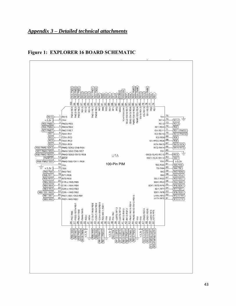
Appendix 3 – Detailed technical attachments
Figure 1: EXPLORER 16 BOARD SCHEMATIC

44
Figure 2: EXPLORER 16 BOARD SCHEMATIC (BOARD MOUNTED
PIC24FJ128GA010 MCU, WHEN INSTALLED)
45
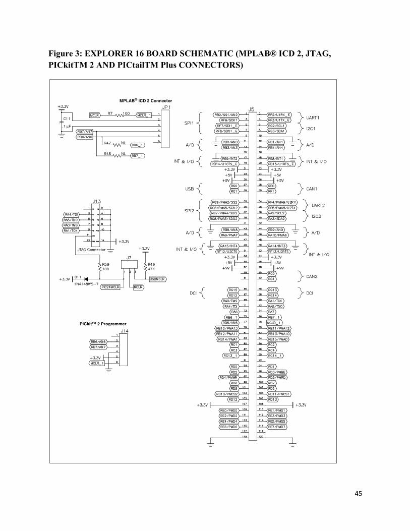
Figure 3: EXPLORER 16 BOARD SCHEMATIC (MPLAB® ICD 2, JTAG,
PICkitTM 2 AND PICtailTM Plus CONNECTORS)
46
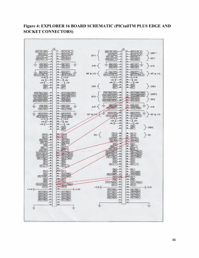
Figure 4: EXPLORER 16 BOARD SCHEMATIC (PICtailTM PLUS EDGE AND
SOCKET CONNECTORS)

47
Figure 5: Pin Diagrams
PIC24FJ128GA010 FAMILY
DS39747D-page 4 Preliminary ã 2007 Microchip Technology Inc.
Pin Diagrams (Continued))
92
94
93
91
90
89
88
87
86
85
84
83
82
81
80
79
78
20
2
3
4
5
6
7
8
9
10
11
12
13
14
15
16
65
64
63
62
61
60
59
56
45
44
43
42
41
40
39
28
29
30
31
32
33
34
35
36
37
38
17
18
19
21
22
95
1
76
77
72
71
70
69
68
67
66
75
74
73
58
57
24
23
25
96
98
97
99
27
46
47
48
49
55
54
53
52
51
100
PM
RD
/CN
14
/RD
5P
MW
R/O
C5/C
N13/R
D4
CN
19/R
D1
3
IC5
/RD
12
PM
BE
/OC
4/R
D3
OC
3/R
D2
OC
2/R
D1
RA
7R
A6
PM
D2
/RE
2R
G1
3
RG
12
RG
14
PM
D1
/RE
1
PM
D0
/RE
0
RG
0
PM
D4
/RE
4
PM
D3
/RE
3
RF
0
SOSCI/CN1/RC13
OC1/RD0
IC3/PMCS2/RD10
IC2/RD9
IC1/RTCC/RD8
IC4/PMCS1/RD11
INT4/RA15
INT3/RA14
OSC2/CLKO/RC15
OSC1/CLKI/RC12
VDD
SCL1/RG2
SCK1/INT0/RF6
SDI1/RF7
SDO1/RF8
SDA1/RG3
U1RX/RF2
U1TX/RF3
VSS
SOSCO/T1CK/CN0/RC14
PM
A6/V
RE
F+
/RA
10
PM
A7
/VR
EF-/
RA
9
AV
DD
AV
SS
C1O
UT
/AN
8/R
B8
C2O
UT
/AN
9/R
B9
PM
A1
3/C
VR
EF/A
N1
0/R
B1
0
PM
A1
2/A
N11/R
B11
VD
D
U2C
TS
/RF
12
U2R
TS
/BC
LK
2/R
F1
3
U1C
TS
/CN
20/R
D1
4
U1
RT
S/B
CL
K1
/CN
21
/RD
15
VD
D
VS
S
PG
C2
/EM
UC
2/A
N6
/OC
FA
/RB
6
PG
D2
/EM
UD
2/A
N7
/RB
7
PM
A8
/U2T
X/C
N18
/RF
5
PM
A9/U
2R
X/C
N17
/RF
4
PMD5/RE5
PMD6/RE6
PMD7/RE7
T2CK/RC1
T3CK/RC2
T4CK/RC3
T5CK/RC4
PMA5/SCK2/CN8/RG6
VDD
TMS/RA0
INT1/RE8
INT2/RE9
C1IN+/AN5/CN7/RB5
C1IN-/AN4/CN6/RB4
C2IN+/AN3/CN5/RB3
C2IN-/AN2/SS1/CN4/RB2
PMA4/SDI2/CN9/RG7
PMA3/SDO2/CN10/RG8
PGC1/EMUC1/AN1/CN3/RB1
PGD1/EMUD1/AN0/CN2/RB0
VDD
RG15
PMA2/SS2/CN11/RG9
MCLR
PM
A11
/AN
12/R
B1
2
PM
A1
0/A
N1
3/R
B1
3
PM
A1
/AN
14/R
B1
4
PM
A0
/AN
15
/OC
FB
/CN
12
/RB
15
RG
1
RF
1
EN
VR
EG
CN
15/R
D6
TDO/RA5
SDA2/RA3
SCL2/RA2
VSS
VS
S
VSS
VC
AP/V
DD
CO
RE
TDI/RA4
TC
K/R
A1
100-Pin TQFP
50
26
CN
16/R
D7
PIC24FJXXGA010PIC24FJXXXGA010
48
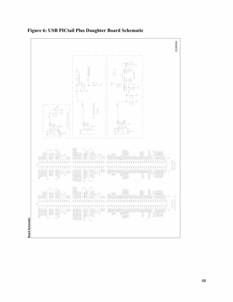
Figure 6: USB PICtail Plus Daughter Board Schematic
US
B P
ICta
ilô
Plu
s D
au
gh
ter
Bo
ard
Bo
ard
Sc
he
mati
c
DS
39
90
9A

49
Figure 7: Pin Diagrams
ã 2008 Microchip Technology Inc. Preliminary DS39897B-page 5
PIC24FJ256GB110 FAMILY
Pin Diagram (100-Pin TQFP)
92
94
93
91
90
89
88
87
86
85
84
83
82
81
80
79
78
20
2
3
4
5
6
7
8
9
10
11
12
13
14
15
16
65
64
63
62
61
60
59
26
56
45
44
43
42
41
40
39
28
29
30
31
32
33
34
35
36
37
38
PIC24FJXXXGB110
17
18
19
21
22
95
1
76
77
72
71
70
69
68
67
66
75
74
73
58
57
24
23
25
96
98
97
99
27
46
47
48
49
50
55
54
53
52
51
100
PM
RD
/RP
20
/CN
14/R
D5
PM
WR
/RP
25
/CN
13/R
D4
CN
19
/RD
13
RP
I42
/CN
57/R
D12
RP
22/P
MB
E/C
N52/R
D3
DP
H/R
P2
3/C
N51
/RD
2
RP
24/V
CP
CO
N/C
N50/R
D1
CN
40
/RA
7
CN
39
/RA
6
PM
D2/C
N60/R
E2
CN
80
/RG
13
CN
79
/RG
12
CN
81
/RG
14
PM
D1/C
N59/R
E1
PM
D0/C
N58/R
E0
CN
77
/RG
0
PM
D4/C
N62/R
E4
PM
D3/C
N61/R
E3
VB
US
ST/V
CM
PS
T1
/CN
68/R
F0
VC
AP/V
DD
CO
RE
SOSCI/C3IND/CN1/RC13
RP11/DMH/CN49/INT0/RD0
RP3/PMCS2/CN55/RD10
RP4/DPLN/CN54/RD9
RP2/DMLN/RTCC/CN53/RD8
RP12/PMCS1/CN56/RD11
RPI35/SDA1/CN44/RA15
RPI36/SCL1/CN43/RA14
OSCO/CLKO/CN22/RC15
OSCI/CLKI/CN23/RC12
VDD
D+/RG2
VUSB
VBUS
RP15/CN74/RF8
D-/RG3
RP30/CN70/RF2
RP16/USBID/CN71/RF3
VSS
RPI37/SOSCO/C3INC/T1CK/
PM
A6
/VR
EF+
/CN
42/R
A1
0
PM
A7/V
RE
F-/
CN
41/R
A9
AV
DD
AV
SS
RP
8/A
N8/C
N2
6/R
B8
RP
9/A
N9/C
N2
7/R
B9
AN
10
/CV
RE
F/P
MA
13/C
N2
8/R
B1
0
AN
11/P
MA
12/C
N29/R
B11
VD
D
RP
I32/C
N75/R
F12
RP
31/C
N76/R
F13
VS
S
VD
D
RP
5/C
N2
1/R
D15
RP
I43/C
N2
0/R
D14
PG
EC
2/A
N6/R
P6/C
N2
4/R
B6
PG
ED
2/R
CV
/RP
7/A
N7/C
N2
5/R
B7
RP
17/P
MA
8/C
N18/R
F5
RP
10/P
MA
9/C
N17/R
F4
PMD5/CN63/RE5
PMD6/SCL3/CN64/RE6
PMD7/SDA3/CN65/RE7
RPI38/CN45/RC1
RPI39/CN46/RC2
RPI40/CN47/RC3
RPI41/CN48/RC4
PMA5/RP21/C1IND/CN8/RG6
VDD
TMS/CN33/RA0
RPI33/CN66/RE8
RPI34/CN67/RE9
PGEC3/RP18/VBUSON/C1INA/AN5/CN7/RB5
VPIO/C2INA/AN3/CN5/RB3
VMIO/RP13/C2INB/AN2/CN4/RB2
RP26/PMA4/C1INC/CN9/RG7
RP19/PMA3/C2IND/CN10/RG8
PGEC1/RP1/AN1/CN3/RB1
PGED1/RP0/AN0/CN2/RB0
CN82/RG15
VDD
RP27/PMA2/C2INC/CN11/RG9
MCLR
AN
12
/CT
ED
2/P
MA
11/C
N3
0/R
B12
AN
13
/CT
ED
1/P
MA
10/C
N31
/RB
13
CT
PLS
/RP
14
/PM
A1/A
N14
/CN
32
/RB
14
RP
29/P
MA
0/A
N15/R
EF
O/C
N12
/RB
15
CN
78
/RG
1
VC
MP
ST2/C
N69/R
F1
C3IN
A/C
N16/R
D7
C3IN
B/C
N15/R
D6
TDO/CN38/RA5
SDA2/CN36/RA3
SCL2/CN35/RA2
VSS
VS
S
VSS
EN
VR
EG
TDI/CN37/RA4
TC
K/C
N3
4/R
A1
PGED3/RP28/USBOEN/C1INB/AN4/CN6/RB4
Legend: RPn and RPIn represent remappable pins for Peripheral Pin Select feature.
CN0/RC14

50
Figure 8: PIC24FJ256GB110 PIM
PIC24FJ256GB110 PIM Manual
Board Schematic
DS39908ADS39909A
VSS
RA
7
VD
DR
G1
VD
D
RD
2
RB
7/A
N7
RE3/P
MPD
3
VD
DRG
12
RB
9/A
N9
RE0/P
MPD
0
VSS
RG
2/S
CL1
RF0/P
MPC
S2
RD
7/S
CL2
VSS
RD
4/P
MP
WR
RD
15
RD
3/P
MP
BE
RA
9/P
MPA
7RE2/P
MPD
2
RG
14
RB10/P
MPA
13
RF12/U
2C
TS
VR
EG
RB14/P
MP
A1
RD
6/S
DA
2
RD
13
RF4/P
MPA
9/U
2RX
RF13/U
2RTS
RB
13/P
MPA
10
RE6/PMPD6
RG15
RF3/U1TX
RF8/SDO1
VBUS
RG3/SDA1
RG2/SCL1
RA3
RA4
VDD
OSC1
VSS
RA14/INT3
RD8
RD9
RD11
RD0
RC14
VSSVSS
RC4
RA2
RA3
RA5
VDD
VSS
RD8
VSS
VD
D
VSS
RA
1
RG
0
RA
6
VSS
VSS
RD
14
RD
15
RD
1
RF2/U1RX
RA5
RA2
RA15/INT4
RC13
RD10
VDD
RB
6/A
N6
RE4/P
MPD
4
VSS
RB
8/A
N8
RE1/P
MPD
1
RG
13
RE2/P
MPD
2
RF3/U
1TX
VD
D
RA
1RF1/P
MPC
S1
RG
3/S
DA
1
RA
6
RA
7
RD
5/P
MPRD
RD
6/S
DA
2
VD
D
RD
14
RG
1
RD
13
RD
1
RG
0
RD2
RA4
RC3
RD0
RD9
VSS
RB6/A
N6
RB7/A
N7
RE4/P
MPD
4
RE3/P
MPD
3
RB8/A
N8
RA
10/P
MPA
6
RB9/A
N9
RE1/P
MPD
1
RE0/P
MPD
0
RG
13
RG
12
RB11/P
MPA
12
RF13/U
2R
TS
RF1/P
MPC
S1
RF0/P
MPC
S2
RB15/P
MP
A0
RB12/P
MPA
11
RB13/P
MPA
10
VSS
VC
AP/V
DD
CO
RE
RD
5/P
MPRD
RD
4/P
MPW
R
RD
7/S
CL2
RF5/P
MPA
8/U
2TX
VSS
RD
3/P
MPBE
RD
12
VSS
RA
10/P
MPA
6
RA
9/P
MPA
7
RB
11/P
MPA
12
RB
10/P
MPA
13
RB
15/P
MPA
0
RB
14/P
MPA
1
RB
12/P
MPA
11
RF12/U
2C
TS
RF5/P
MPA
8/U
2TX
RF4/P
MPA
9/U
2RX
RB0/AN0
RB2/SS1/AN2
RB3/AN3
RB5/AN5
RE9/INT2
RA0
VDD
RG9/PMPA2/SS2
MCLR
RG7/PMPA4/SDI2
RG6/PMPA5/SCK2
RC3
RC2
RE7/PMPD7
VDD
RB1/AN1
RB2/SS1/AN2
RB4/AN4
RB5/AN5
RE8/INT1
RA0
RG9/PMPA2/SS2
RG8/PMPA3/SDO2
RG7/PMPA4/SDI2
RG14
RG15
RC1
RE7/PMPD7
RE5/PMPD5
VDD
RF8/SDO1
RB0/AN0
RA15/INT4
OSC2
RD12
RD10
RD11
RC13
RC14
RB4/AN4
RB1/AN1
VSS
RE8/INT1
RG8/PMPA3/SDO2
RC4
RE5/PMPD5
RC1
VDD
VSS
RB10/PMPA13
OSC2
RB3/AN3
VDD
RE9/INT2
MCLR
RG6/PMPA5/SCK2
RE6/PMPD6
RC2
VDD
VBUS
RF2/U1RX
RA14/INT3
OSC1

51
Figure 9: Description of MRF49XA transceivers
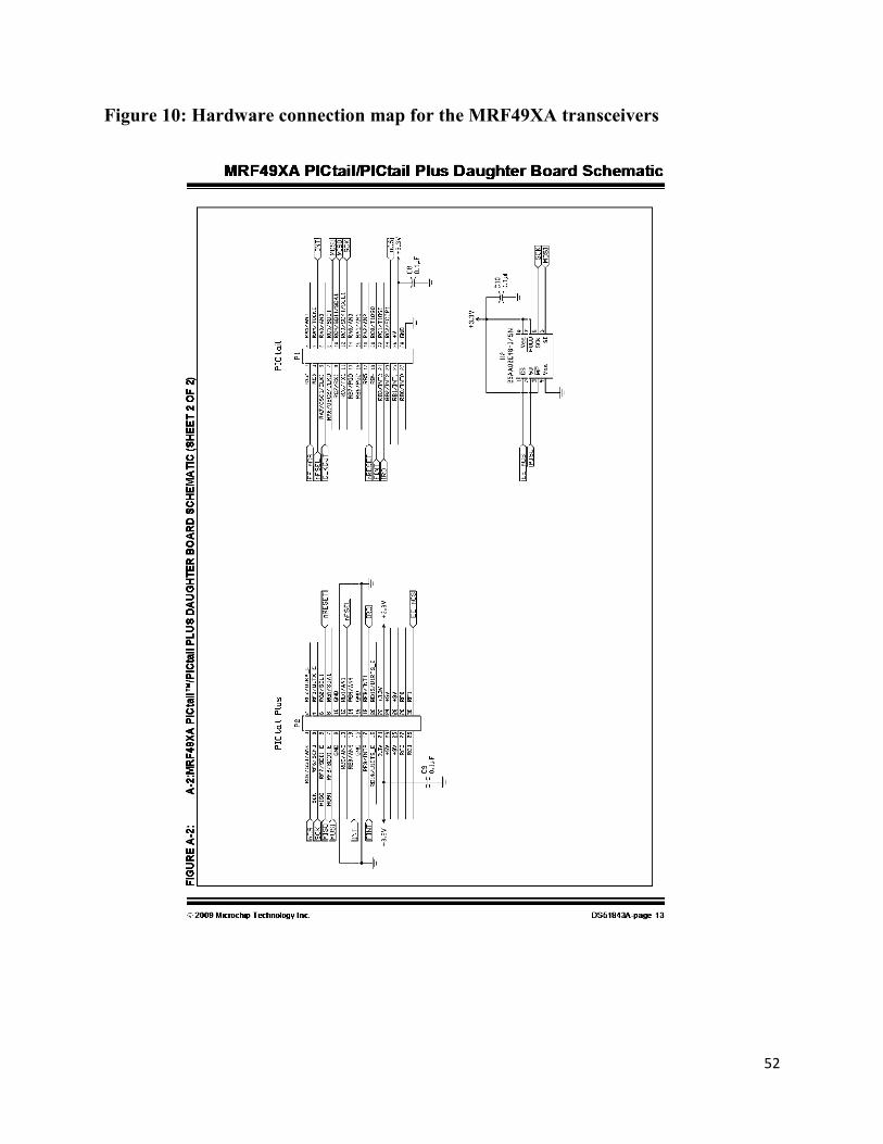
52
Figure 10: Hardware connection map for the MRF49XA transceivers
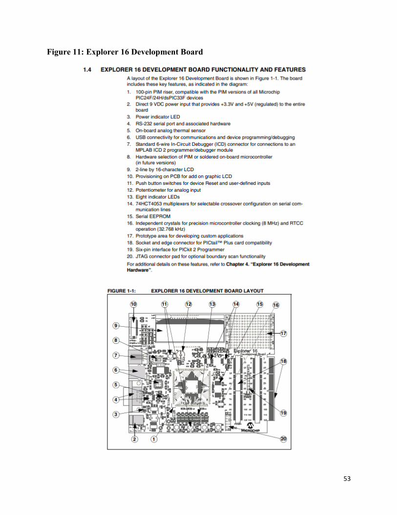
53
Figure 11: Explorer 16 Development Board
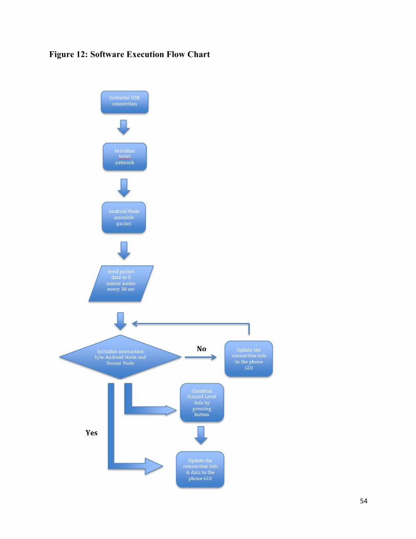
54
Figure 12: Software Execution Flow Chart


![Smart UVI Checker - ISweek · Smart UVI Checker GUVA-S12SC-LM01 Connect Jack (Ear Jack) [Sensor] Sensor unit (Aluminum) [Connected] Connect to Smart phone ear jack Keyword in Google](https://img.pdfslide.us/doc/110x75/5fd4a878a93a72149d1fa409/smart-uvi-checker-isweek-smart-uvi-checker-guva-s12sc-lm01-connect-jack-ear-jack.jpg)