Embed Size (px)
Citation preview
Smart Charging of Future Electric Vehicles Using Roadway Infrastructure
Project No. 18ITSTSA03
Lead University: University of Texas at San Antonio
Collaborative Universities: University of New Mexico
Final Report
August 2019

i
Disclaimer
The contents of this report reflect the views of the authors, who are responsible for the facts and the accuracy of the information presented herein. This document is disseminated in the interest of information exchange. The report is funded, partially or entirely, by a grant from the U.S. Department of Transportation’s University Transportation Centers Program. However, the U.S. Government assumes no liability for the contents or use thereof.
Acknowledgements
The authors would like to acknowledge the support by the Transportation Consortium of South-Central States (Tran-SET).

ii
TECHNICAL DOCUMENTATION PAGE 1. Project No. 18ITSTSA03
2. Government Accession No.
3. Recipient’s Catalog No.
4. Title and Subtitle Smart Charging of Future Electric Vehicles using Roadway Infrastructure
5. Report Date Aug. 2019
6. Performing Organization Code 7. Author(s) PI: Sara Ahmed https://orcid.org/0000-0003-0935-5011 Co-PI: Ethan Ahn https://orcid.org/0000-0002-0807-2071 Co-PI: Mahmoud Reda Taha https://orcid.org/0000-0002-3707-9336 Co-PI: Samer Dessouky https://orcid.org/0000-0002-6799-6805 Post-Doc: Moneeb Genedy https://orcid.org/0000-0002-0037-5086 GRA: Daniel Fernandez https://orcid.org/0000-0003-3421-2207 GRA: Ann Sebastian https://orcid.org/0000-0002-0345-7204 GRA: Patience Raby https://orcid.org/0000-0002-1149-9033
8. Performing Organization Report No.
9. Performing Organization Name and Address Transportation Consortium of South-Central States (Tran-SET)
10. Work Unit No. (TRAIS)
University Transportation Center for Region 6 3319 Patrick F. Taylor Hall, Louisiana State University, Baton Rouge, LA 70803
11. Contract or Grant No. 69A3551747106
12. Sponsoring Agency Name and Address United States of America Department of Transportation
13. Type of Report and Period Covered Final Research Report Mar. 2018 – Mar. 2019
Research and Innovative Technology Administration 14. Sponsoring Agency Code
15. Supplementary Notes Report uploaded and accessible at Tran-SET's website (http://transet.lsu.edu/) 16. Abstract Inspired by the fact that there is an immense amount of renewable energy sources available on the roadways such as mechanical pressure and frictional heat, this study presented the development and implementation of an innovative charging technique for future electric vehicles (EVs) by fully utilizing the existing roadways and the state-of-the-art nanotechnology and power electronics. The project introduced a novel wireless charging system, SIC (Smart Illuminative Charging), that uses LEDs powered by piezoelectric nanomaterials as the energy transmitter source and thin film solar panels placed at the bottom of the EVs as the receiver, which is then poised to deliver the harvested energy to the vehicle’s battery. Through the project, the energy-harvestable 2D nanomaterials (EH2Ns) were tested for their mechanical-to-electrical energy conversion capabilities and the relatively large-area EH2N samples (2cm x 2cm) produced high output voltages of up to 52mV upon mechanical pressure. An electrically conductive glass fiber reinforced polymer (GFRP) was developed to be used as physical support in the integrated SIC system. Furthermore, a lab-scale prototype device was developed to testify the mechanism of illuminative charging. The project team was able to prove the feasibility of SIC concept and the start to end conversion efficiency was calculated to be 40%. The project team also provided field implementation recommended framework based on the results from the small-scale prototype developed. The framework discussed how the developed SIC can be implemented in the field and what are the expected outcomes. The team recommended inserting the EH2N embedded in the GFRP, the LEDs and the needed circuitry in the wheel path of the vehicles on the pavement by cutting a sawtooth compartment with a width of 18’’ and a length of 8’ every couple of miles. On the vehicle, a PV array will be placed on the underside between the wheel wells of each side of the EV to capture the illumination from the LEDs embedded in the roadway. The detailed strategy is presented in this report.
17. Key Words Smart Charging, Electric vehicles, 2D Nanomaterials, Piezoelectric effect, LEDs, solar panels
18. Distribution Statement No restrictions. This document is available through the National Technical Information Service, Springfield, VA 22161.
19. Security Classif. (of this report) Unclassified
20. Security Classif. (of this page) Unclassified
21. No. of Pages 49
22. Price
Form DOT F 1700.7 (8-72) Reproduction of completed page authorized.

iii
SI* (MODERN METRIC) CONVERSION FACTORS APPROXIMATE CONVERSIONS TO SI UNITS
Symbol When You Know Multiply By To Find Symbol LENGTH
in inches 25.4 millimeters mm ft feet 0.305 meters m yd yards 0.914 meters m mi miles 1.61 kilometers km
AREA in2 square inches 645.2 square millimeters mm2
ft2 square feet 0.093 square meters m2
yd2 square yard 0.836 square meters m2
ac acres 0.405 hectares ha mi2 square miles 2.59 square kilometers km2
VOLUME fl oz fluid ounces 29.57 milliliters mL gal gallons 3.785 liters L ft3 cubic feet 0.028 cubic meters m3
yd3 cubic yards 0.765 cubic meters m3
NOTE: volumes greater than 1000 L shall be shown in m3
MASS oz ounces 28.35 grams glb pounds 0.454 kilograms kgT short tons (2000 lb) 0.907 megagrams (or "metric ton") Mg (or "t")
TEMPERATURE (exact degrees) oF Fahrenheit 5 (F-32)/9 Celsius oC
or (F-32)/1.8 ILLUMINATION
fc foot-candles 10.76 lux lx fl foot-Lamberts 3.426 candela/m2 cd/m2
FORCE and PRESSURE or STRESS lbf poundforce 4.45 newtons N lbf/in2 poundforce per square inch 6.89 kilopascals kPa
APPROXIMATE CONVERSIONS FROM SI UNITS Symbol When You Know Multiply By To Find Symbol
LENGTHmm millimeters 0.039 inches in m meters 3.28 feet ft m meters 1.09 yards yd km kilometers 0.621 miles mi
AREA mm2 square millimeters 0.0016 square inches in2
m2 square meters 10.764 square feet ft2
m2 square meters 1.195 square yards yd2
ha hectares 2.47 acres ac km2 square kilometers 0.386 square miles mi2
VOLUME mL milliliters 0.034 fluid ounces fl oz L liters 0.264 gallons gal m3 cubic meters 35.314 cubic feet ft3
m3 cubic meters 1.307 cubic yards yd3
MASS g grams 0.035 ounces ozkg kilograms 2.202 pounds lbMg (or "t") megagrams (or "metric ton") 1.103 short tons (2000 lb) T
TEMPERATURE (exact degrees) oC Celsius 1.8C+32 Fahrenheit oF
ILLUMINATION lx lux 0.0929 foot-candles fc cd/m2 candela/m2 0.2919 foot-Lamberts fl
FORCE and PRESSURE or STRESS N newtons 0.225 poundforce lbf kPa kilopascals 0.145 poundforce per square inch lbf/in2
iv
TABLE OF CONTENTS TECHNICAL DOCUMENTATION PAGE .................................................................................. ii
TABLE OF CONTENTS ............................................................................................................... iv
LIST OF FIGURES ....................................................................................................................... vi
ACRONYMS, ABBREVIATIONS, AND SYMBOLS .............................................................. viii
EXECUTIVE SUMMARY ........................................................................................................... ix
1. INTRODUCTION ...................................................................................................................... 1
2. OBJECTIVES ............................................................................................................................. 3
3. LITERATURE REVIEW ........................................................................................................... 4
3.1. Electric Vehicles Charging Stations .................................................................................... 4
3.2. Wireless Charging Methods for Electric Vehicles (EVs) .................................................... 4
3.2.1. Wireless Power Transfer (WPT) for EV Applications ................................................. 5
3.2.2. Solar-Powered EVs ....................................................................................................... 5
3.3. Other Wireless Power Transfer Systems ............................................................................. 6
3.4. Energy Harvesting using Roadway Infrastructure ............................................................... 6
3.4.1. Solar Pavements ............................................................................................................ 7
3.4.2. Asphalt Solar Collectors ............................................................................................... 7
3.4.3. Nanomaterials ............................................................................................................... 8
3.5. Fiber Reinforced Polymer Modified Nanocomposite Overlay ............................................ 9
3.6. Power Conditioning Circuits for Nanomaterials Energy Harvesting Systems .................... 9
4. METHODOLOGY ................................................................................................................... 11
4.1. Light Emitting Diodes (LEDs) and Photovoltaic (Solar) Panels ....................................... 11
4.1.1. Photovoltaic Solar System .......................................................................................... 11
4.1.2. Light Emitting Diodes (LEDs) .................................................................................... 13
4.2. Energy-Harvestable 2D Nanomaterials (EH2N) ............................................................... 14
4.2.1. Sample Preparation ..................................................................................................... 15
4.2.2. Structural Characterization ......................................................................................... 15
4.2.3. Piezoelectric Characterization..................................................................................... 16
4.2.4. Testing with Commercially Available Nanomaterial Samples ................................... 17
4.2.5. Thermoelectric Property of EH2N .............................................................................. 18

v
4.3. Alternate Piezoelectric Materials Tested ........................................................................... 18
4.3.1. Piezoelectric Ceramic Crystal Disks ........................................................................... 18
4.3.2. Shear-Mode Piezoelectric Plates ................................................................................. 19
4.3.3. Thin-Film Piezoelectric Sheets ................................................................................... 19
4.4. Fabrication and Testing of Electrically Conductive GFRP ............................................... 20
4.5. Power Delivery Circuit Design .......................................................................................... 23
4.6. Lab-scale Proof-of-Concept Design of the Smart Charging System ................................. 24
4.6.1. Solar Panel Configurations ......................................................................................... 24
4.6.2. MPPT Circuit for Solar Panels and Communication .................................................. 26
4.6.3. Sensing Circuit for LEDs ............................................................................................ 26
5. ANALYSIS AND FINDINGS ................................................................................................. 28
5.1. Harvested Voltage from EH2N (Piezoelectric effect) ....................................................... 28
5.2. Mechanical and Electrical Measurements of GFRP .......................................................... 29
5.3. Test Results for the Lab-scale Prototype ........................................................................... 31
5.3.1. Stationary Tests with Indoor Setting and Artificial LEDs .......................................... 31
5.3.2. Stationary Tests Comparison of Indoors and Outdoors Settings ................................ 32
5.3.3. Test of the Lab-scale Prototype under Motion with Indoor Setting and Artificial LEDs ............................................................................................................................................... 34
5.4. System Conversion Efficiencies ........................................................................................ 36
5.5. Recommended Strategy for the Smart Charging System .................................................. 37
5.5.1. System Embedded in Infrastructure ............................................................................ 37
5.2.1. System for Electrical Vehicle (EV) ............................................................................ 39
6. CONCLUSIONS....................................................................................................................... 41
REFERENCES ............................................................................................................................. 42

vi
LIST OF FIGURES Figure 1. Schematic of the smart charging system for vehicles and roadway infrastructures of the
future. .......................................................................................................................................... 3
Figure 2. Wireless power transfer. .................................................................................................. 5
Figure 3. Example of solar powered EV. ........................................................................................ 6
Figure 4. Example of solar pavement. ............................................................................................ 7
Figure 5. Asphalt solar collector. .................................................................................................... 8
Figure 6. First, second, and third generation solar cells. .............................................................. 12
Figure 7. EH2N grown by CVD. .................................................................................................. 15
Figure 8. Raman characterization data of EH2N grown on a SiO2/Si substrate. .......................... 16
Figure 9. PFM measurements of EH2N. The observed phase shift between the two different voltage polarities indicates that the EH2N thin film expands and contracts with the electric field direction (i.e., piezoelectric). .................................................................................................... 17
Figure 10. Mechanical exfoliation of commercially available MoS2 crystals. ............................. 18
Figure 11. Piezoelectric ceramic crystal disks. ............................................................................. 19
Figure 12. Shear-mode Piezoelectric plate testing. ....................................................................... 19
Figure 13. Piezoelectric thin films. ............................................................................................... 20
Figure 14. GFRP fabrication using vacuum hand lay-up technique. ............................................ 21
Figure 15. SEM images of CNFs in the epoxy matrix; (a) 0.5 wt %; (b) 2.0 wt %; and (c) a close view of 2.0 wt % CNFS shows the formation of conductive network inside epoxy. ............... 22
Figure 16. Schematic of electrical resistance measurement of glass fiber composite coupons during tension tests. .............................................................................................................................. 22
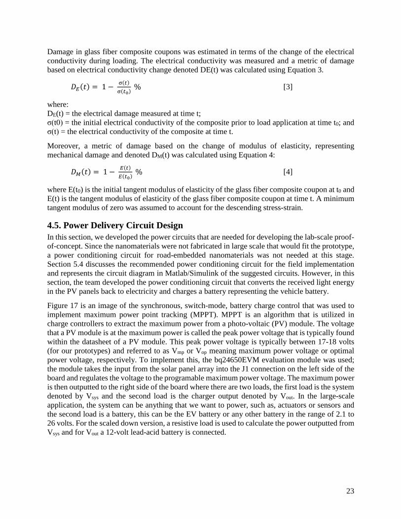
Figure 17. Texas Instruments: synchronous, switch-mode, and battery charge controller for solar power wiring. ............................................................................................................................ 24
Figure 18. Three solar panels frames constructed for lab-scale prototype. .................................. 25
Figure 19. Lab-scale proof-of-concept prototype. ........................................................................ 25
Figure 20. Circuit diagram for power delivery from solar panels. ............................................... 26
Figure 21. Wiring diagram of a HC-SR04 ultrasonic sensor. ....................................................... 26
Figure 22. Wiring diagram of the JBtek 4 Channel DC 5V relay module. ................................... 27
Figure 23. Bending experiment and the produced output voltage. ............................................... 28
Figure 24. Two EH2N samples connected to test the scalability. ................................................ 29
vii
Figure 25. Stress-strain curves of GFRP and electrically conductive GFRP incorporating 2.0% CNFs. ........................................................................................................................................ 30
Figure 26. Stress-electrical damage (DE) and stress-mechanical damage (DM) for glass fiber composite incorporating CNFs under monotonically increasing static tension stress. ............. 30
Figure 27. Electrical characteristic of the Renogy 30 W solar panel lighted from LEDs. ........... 31
Figure 28. Electrical characteristic of the EcoWorthy 10 W solar panel lighted from LEDs. .... 32
Figure 29. Electrical characteristic of the Second Generation 13W solar panel lighted from LEDs. .................................................................................................................................................. 32
Figure 30. Electrical characteristic of the Renogy 30 W solar panel lighted from LEDs (Orange) and from direct sunlight (Blue) respectively. ........................................................................... 33
Figure 31. Electrical characteristic of the 13W SolarKingdom solar panel lighted from LEDs (Orange) and from direct sunlight (Blue) respectively. ............................................................ 33
Figure 32. Electrical characteristic of the 10W HQST solar panel lighted from LEDs (Orange) and from direct sunlight (Blue) respectively. .................................................................................. 34
Figure 33. Sweeping resistive load to capture the maximum power output for one Renorgy 30W panel, two-13W Sunkingdom panel and three of the 10 W EcoWorthy panels. ...................... 35
Figure 34. Output voltage, current and power measured while simulated vehicle in motion using the 30W Renogy solar panel and under different speeds: (a) 1.12m/s, (b) 2.24m/s and (c) 3m/s, from left to right respectively. .................................................................................................. 35
Figure 35. Output voltage, current, and power measured while simulated vehicle in motion using the 2-13W SunKingdom solar panels and under different speeds: (a) 1.12m/s, (b) 2.24m/s and (c) 3m/s, from left to right respectively. ................................................................................... 36
Figure 36. Output voltage, current, and power measured while simulated vehicle in motion using the 3-10W EcoWorthy solar panels and under different speeds: (a) 1.12m/s, (b) 2.24m/s and (c) 3m/s, from left to right respectively. ......................................................................................... 36
Figure 37. Flowchart of the different energy conversion steps in the SIC system with energy efficiency. ................................................................................................................................. 37
Figure 38. The sections of a lane (120)......................................................................................... 38
Figure 39. Suggested circuitry for the embedded roadway. ......................................................... 39
Figure 40. Suggested circuitry for the electric vehicle system. .................................................... 40
Figure 41. Monocrystalline solar cells. ......................................................................................... 40
viii
ACRONYMS, ABBREVIATIONS, AND SYMBOLS AFRP Aramid Fiber Reinforced Polymer
BFRP Basalt Fiber Reinforced Polymer
CFRP Carbon Fiber Reinforced Polymer
CNF Epoxy-Carbon Nanofiber
DOE Department of Energy
EH2N Energy-Harvestable 2D Nanomaterial
EV Electric Vehicles
FRP Fiber Reinforced Polymer
GFRP Glass Fiber Reinforced Polymer
LED Light Emitting Diode
LUX Lumens per Watt
MPPT Maximum Power Point Tracking
PV Photovoltaic
SIC Smart Illuminative Charging
TPMN Transparent Polymer Modified Nanocomposite
WPT Wireless Power Transfer
UNM University of New Mexico
UTSA University of Texas at San Antonio
ix
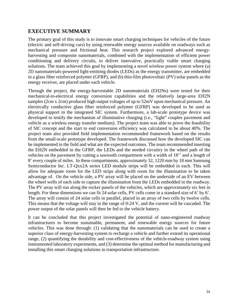
EXECUTIVE SUMMARY The primary goal of this study is to innovate smart charging techniques for vehicles of the future (electric and self-driving cars) by using renewable energy sources available on roadways such as mechanical pressure and frictional heat. This research project explored advanced energy-harvesting and composite nanomaterials, combined with the implementation of efficient power conditioning and delivery circuits, to deliver innovative, practically viable smart charging solutions. The team achieved this goal by implementing a novel wireless power system where (a) 2D nanomaterials-powered light-emitting diodes (LEDs) as the energy transmitter, are embedded in a glass fiber reinforced polymer (GFRP), and (b) thin-film photovoltaic (PV) solar panels as the energy receiver, are placed under each vehicle.
Through the project, the energy-harvestable 2D nanomaterials (EH2Ns) were tested for their mechanical-to-electrical energy conversion capabilities and the relatively large-area EH2N samples (2cm x 2cm) produced high output voltages of up to 52mV upon mechanical pressure. An electrically conductive glass fiber reinforced polymer (GFRP) was developed to be used as physical support in the integrated SIC system. Furthermore, a lab-scale prototype device was developed to testify the mechanism of illuminative charging (i.e., “light” couples pavement and vehicle as a wireless energy transfer medium). The project team was able to prove the feasibility of SIC concept and the start to end conversion efficiency was calculated to be about 40%. The project team also provided field implementation recommended framework based on the results from the small-scale prototype developed. The framework discussed how the developed SIC can be implemented in the field and what are the expected outcomes. The team recommended inserting the EH2N embedded in the GFRP, the LEDs and the needed circuitry in the wheel path of the vehicles on the pavement by cutting a sawtooth compartment with a width of 18’’ and a length of 8’ every couple of miles. In these compartments, approximately 32, 1220 mm by 18 mm Samsung Semiconductor Inc. LT-Qxx2A series LED module strips will be embedded in each. This will allow for adequate room for the LED strips along with room for the illumination to be taken advantage of. On the vehicle side, a PV array will be placed on the underside of an EV between the wheel wells of each side to capture the illumination from the LEDs embedded in the roadway. The PV array will run along the rocker panels of the vehicles, which are approximately six feet in length. For these dimensions we can fit 24 solar cells, PV cells come in a standard size of 6’ by 6’. The array will consist of 24 solar cells in parallel, placed in an array of two cells by twelve cells. This means that the voltage will stay in the range of 0-24 V, and the current will be cascaded. The power output of the solar panels will then be fed to the vehicle battery.
It can be concluded that this project investigated the potential of nano-engineered roadway infrastructures to become sustainable, permanent, and renewable energy sources for future vehicles. This was done through: (1) validating that the nanomaterials can be used to create a superior class of energy-harvesting system to recharge a vehicle and further extend its operational range, (2) quantifying the durability and cost-effectiveness of the vehicle-roadway system using instrumented laboratory experiments, and (3) determine the optimal method for manufacturing and installing this smart charging solutions in transportation infrastructure.
1
1. INTRODUCTION Roadways are an important part of transportation infrastructure, serving as a backbone to enable better mobility for people and goods. Because the roadways greatly impact the economic growth and development of the communities, state-of-the-art research has focused on planning, designing, and constructing roadways to reduce environmental impact, increase sustainability, and improve the efficiency of transport flow. However, due to increasingly large demands for reduced driver stress, independent mobility for non-drivers, and increased safety and in-vehicle infotainment, further research is called for on the development of novel roadways that can adapt for future vehicles (e.g., electric or self-driving cars).
Electric vehicles are promoted as a key contributor to building this sustainable mobility system. They are generally much more energy efficient than those powered by fossil fuels. Increasing the use of these electric cars can result in considerably lower emissions of carbon dioxide and other air pollutants including nitrogen oxides and particulate matter (PM), and therefore decrease the air quality problems and preserve the environment. However, increasing the use of these vehicles requires additional electricity generation to charge their batteries and as a result, the avoided CO2 emissions will be partially offset by additional emissions caused by generating extra electricity. In addition, these future vehicles need to be equipped with a large-capacity battery pack as an energy storage unit to operate for a satisfactory distance. Lithium-ion batteries, the most commonly used battery in today’s electric vehicles (EVs), have an energy density of only 90-100 Wh/kg (1,2), which is very low as compared with that of gasoline (about 12,000 Wh/kg). Therefore, the lithium-ion battery-operated EVs can only operate for about a 300-mile range and then they need to be recharged. In addition to the low energy density, contemporary battery technologies have shortcomings of long charging time, large size and weight, limited lifetime and high cost. To overcome these challenges, alternative charging strategies that utilize renewable energy sources and roadways need to be developed. Currently, the stationary charging systems of EVs fall under three categories, Level 1, 2, and 3 charging stations. Level 1 charging stations use a 120 VAC plug supplying 3-5 miles per hour using a standard outlet. Level 2 EV charging stations are used for both residential and commercial charging stations. They use a 240 V (for residential) or 208 V (for commercial) plug charging at a rate of 10-20 miles per hour. Level 3 charging stations, also known as DC fast chargers, use a 208 V (for commercial) plug or is connected to a 480 V 3-Phase AC source and can charge 80 percent of an EVs battery in 20-30 minutes. Alternatives to stationary charging stations have also been introduced, for example wireless power transfer (WPT) charging (3), and photovoltaic (solar) cars (4). Wireless power transfer (WPT) for EVs has been introduced by using magnetic resonance to create a field between a ground charging coil and a copper coil embedded in a vehicle. A research team from MIT first demonstrated in 2007 that 60 watts of power can be transferred at a 2 meter distance according to the coupled magnetic resonance theory. Many researchers followed this groundbreaking work on wireless power transfer (WPT) mechanism, suggesting innovative circuits and performing system-level analysis with improved control. Despite the popularity and maturity of the WPT technology for EV charging, its relatively high cost and limited distance for power transmission (maximum of 3 ft) still remain a great challenge. Solar power is another method for charging EVs wirelessly without entirely relying on batteries, as energy can be harnessed from the sun and converted into electricity by placing the solar panels on a vehicle’s roof. However, this type of charging solution is only feasible when the sunlight is available (e.g., during the daytime); the vehicle batteries should still be charged using power from the grid during night time. Moreover, solar-powered EVs are still not mature enough

2
to be economically available to customers, largely due to multiple technical and manufacturing challenges in the contemporary PV cell technology such as the engineering tradeoff between cost and energy conversion efficiency.
There are many applications of harvesting energy using the roadway due to multiple renewable energy sources available through roadways: optical (light), thermal (heat), and mechanical (deformation or friction) energies. One form of energy harvesting is solar pavement, a form of pavement that generates electricity by collecting solar power with photovoltaic cells and is installed in various roadway infrastructures. Recent research studies have considered the potential of functional (e.g., piezoelectric or thermoelectric) nanomaterials to generate electricity from mechanical pressure or frictional heat. The reasoning behind this nanomaterials-based energy harvesting system is that the nanomaterial can be embedded inside the roadway pavement or the vehicle tire such that the mechanical or thermal excitation is induced in the nanomaterial by tire loading of the vehicles, producing separation of electrical charges. Although the voltage and power level generated from this nano-generator system may be relatively low, this approach has great potential to advance the energy harvesting technology by miniaturizing the system and facilitating its integration with other existing infrastructures. One example to this is the BH-03 tire by Goodyear that produces electricity by: (1) using thermoelectric materials (like bismuth telluride and tin selenide) to generate electricity from the difference between the hottest and coolest parts of the rubber and (2) using a piezoelectric material from the load on the tires.
3
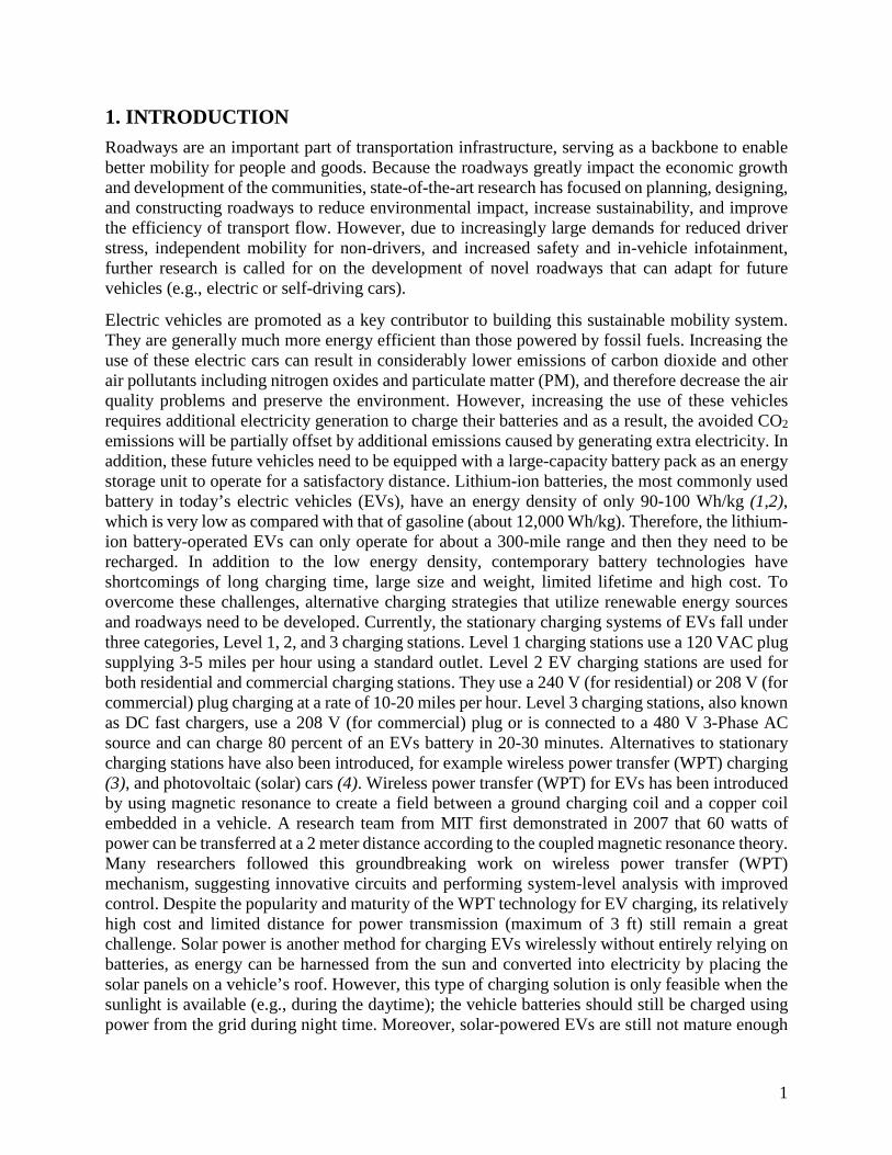
2. OBJECTIVES The primary objective of this project is to introduce an innovative Smart Illuminative Charging (SIC) method for vehicles of the future (electric and self-driving cars) by using renewable energy sources available on roadways such as mechanical pressure and frictional heat. This project introduces a novel wireless power system where: (a) nanomaterials-powered light-emitting diodes (LEDs) as the energy transmitter, are embedded under a transparent polymer modified nanocomposite (TPMN) overlay and (b) thin-film photovoltaic (PV) solar panels as the energy receiver, are placed under each vehicle (see Figure 1). The energy harvested during vehicle motion by using cutting-edge low-dimensional nanomaterials is transferred to the vehicle’s main power supply, i.e., battery. The report will also discuss a lab-scale proof-of-concept prototype for smart charging system for vehicles of the future. The prototype represents the integration of existing roadways, state-of-the-art nanomaterials and power electronics technologies to create a smart, sustainable transportation infrastructure.
Figure 1. Schematic of the smart charging system for vehicles and roadway infrastructures of the future.
4
3. LITERATURE REVIEW In this section, we review state-of-the-art works on wireless electric vehicle (EV) recharging systems, energy-harvesting techniques in roadways, polymer composite materials for civil infrastructure, and power conditioning circuits, and further highlight the novelty of our approach as compared with these previous works.
3.1. Electric Vehicles Charging Stations Electric cars are charged by plugging them into a charger that is connected to the electric grid. EV chargers typically fall under one of three main categories: Level 1 charging stations, Level 2 charging stations, and DC fast chargers (level 3 charging stations). Level 1 chargers use a 120 V AC plug and can be plugged into a standard outlet. Unlike other chargers, Level 1 chargers do not require the installation of any additional equipment. These chargers typically deliver two to five miles of range per hour of charging and are most often used at home. Level 1 chargers are the least expensive option, but they also take the most time to charge the car’s battery. Homeowners typically use these types of chargers to charge their cars overnight. Manufacturers of Level 1 EV chargers include AeroVironment, Duosida, Leviton, and Orion. Level 2 EV charging stations are used for both residential and commercial charging stations. They use a 240 V (for residential) or 208 V (for commercial) plug, and unlike Level 1 chargers, they can’t be plugged into a standard wall outlet. Instead, they are usually installed by a professional electrician. Level 2 charging stations can also be as part of a solar panel system. Level 2 electric car chargers deliver 10 to 60 miles of range per hour of charging. They can fully charge an electric car battery in as little as two hours, making them an ideal option for both homeowners who need fast charging and businesses who want to offer charging stations to customers. Many electric car manufacturers, like Nissan, have their own Level 2 charger products. Other Level 2 charger manufacturers include ClipperCreek, Chargepoint, JuiceBox, and Siemens. DC Fast Chargers (also known as Level 3 charging stations) offer 60 to 100 miles of range for your electric car in just 20 minutes of charging. However, they are typically only used in commercial and industrial applications – they require highly specialized, high-powered equipment to install and maintain. Not all electric cars can be charged with the use of DC Fast Chargers. Most plug-in hybrid EVs don’t have this charging capability, and some all-electric vehicles cannot be charged with a DC Fast Charger. The Mitsubishi “i” and Nissan Leaf are two examples of electric cars that are DC Fast Charger enabled.
3.2. Wireless Charging Methods for Electric Vehicles (EVs) In an effort to eliminate the complex and costly charging system currently available for EVs (e.g., EVs are battery-powered, and recharged at charging stations over limited spots), several alternative charging mechanisms have been investigated, including stationary and dynamic wireless power transfer (WPT) charging (3) and photovoltaic (solar) cells (4).
5
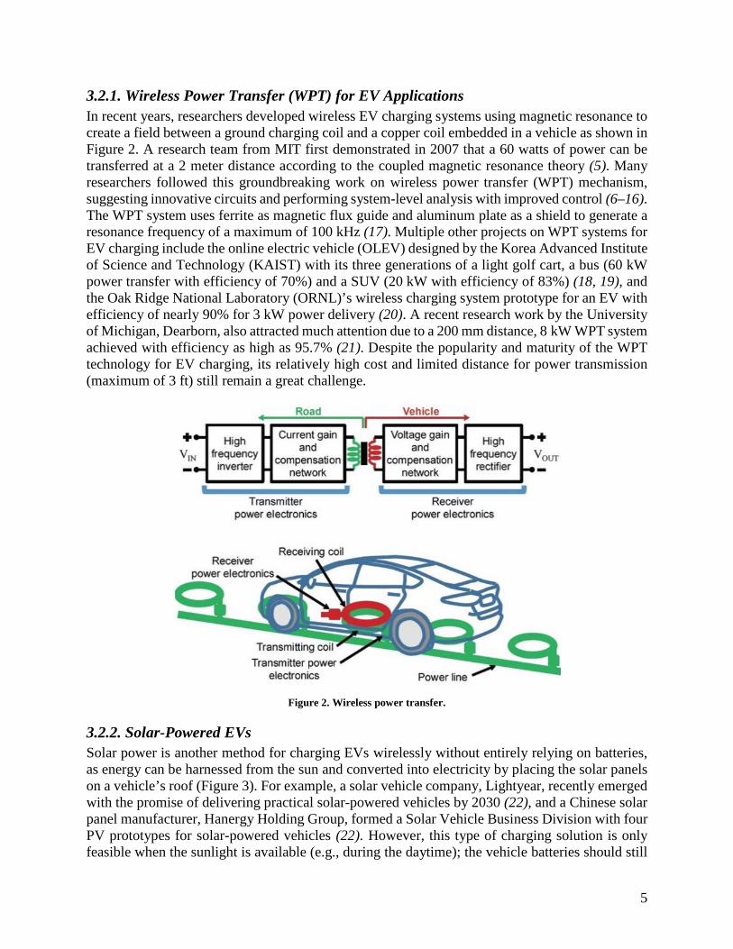
3.2.1. Wireless Power Transfer (WPT) for EV Applications In recent years, researchers developed wireless EV charging systems using magnetic resonance to create a field between a ground charging coil and a copper coil embedded in a vehicle as shown in Figure 2. A research team from MIT first demonstrated in 2007 that a 60 watts of power can be transferred at a 2 meter distance according to the coupled magnetic resonance theory (5). Many researchers followed this groundbreaking work on wireless power transfer (WPT) mechanism, suggesting innovative circuits and performing system-level analysis with improved control (6–16). The WPT system uses ferrite as magnetic flux guide and aluminum plate as a shield to generate a resonance frequency of a maximum of 100 kHz (17). Multiple other projects on WPT systems for EV charging include the online electric vehicle (OLEV) designed by the Korea Advanced Institute of Science and Technology (KAIST) with its three generations of a light golf cart, a bus (60 kW power transfer with efficiency of 70%) and a SUV (20 kW with efficiency of 83%) (18, 19), and the Oak Ridge National Laboratory (ORNL)’s wireless charging system prototype for an EV with efficiency of nearly 90% for 3 kW power delivery (20). A recent research work by the University of Michigan, Dearborn, also attracted much attention due to a 200 mm distance, 8 kW WPT system achieved with efficiency as high as 95.7% (21). Despite the popularity and maturity of the WPT technology for EV charging, its relatively high cost and limited distance for power transmission (maximum of 3 ft) still remain a great challenge.
Figure 2. Wireless power transfer.
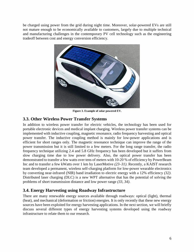
3.2.2. Solar-Powered EVs Solar power is another method for charging EVs wirelessly without entirely relying on batteries, as energy can be harnessed from the sun and converted into electricity by placing the solar panels on a vehicle’s roof (Figure 3). For example, a solar vehicle company, Lightyear, recently emerged with the promise of delivering practical solar-powered vehicles by 2030 (22), and a Chinese solar panel manufacturer, Hanergy Holding Group, formed a Solar Vehicle Business Division with four PV prototypes for solar-powered vehicles (22). However, this type of charging solution is only feasible when the sunlight is available (e.g., during the daytime); the vehicle batteries should still
6
be charged using power from the grid during night time. Moreover, solar-powered EVs are still not mature enough to be economically available to customers, largely due to multiple technical and manufacturing challenges in the contemporary PV cell technology such as the engineering tradeoff between cost and energy conversion efficiency.
Figure 3. Example of solar powered EV.
3.3. Other Wireless Power Transfer Systems In addition to wireless power transfer for electric vehicles, the technology has been used for portable electronic devices and medical implant charging. Wireless power transfer systems can be implemented with inductive coupling, magnetic resonance, radio frequency harvesting and optical power transfer. The inductive coupling method is mainly for low-power applications and is efficient for short ranges only. The magnetic resonance technique can improve the range of the power transmission but it is still limited to a few meters. For the long range transfer, the radio frequency technique utilizing 2.4 and 5.8 GHz frequency has been developed but it suffers from slow charging time due to low power delivery. Also, the optical power transfer has been demonstrated to transfer a few watts over tens of meters with 10-20 % of efficiency by PowerBeam Inc and to transfer a few kWatts over 1 km by LaserMotive (23–31). Recently, a KAIST research team developed a permanent, wireless self-charging platform for low-power wearable electronics by converting near-infrared (NIR) band irradiation to electric energy with a 12% efficiency (32). Distributed laser charging (DLC) is a new WPT alternative that has the potential of solving the problems of short transmission distance and low power range (33, 34).
3.4. Energy Harvesting using Roadway Infrastructure There are many renewable energy sources available through roadways: optical (light), thermal (heat), and mechanical (deformation or friction) energies. It is only recently that these new energy sources have been exploited for energy harvesting applications. In the next section, we will briefly discuss several different types of energy harvesting systems developed using the roadway infrastructure to relate them to our research.
7
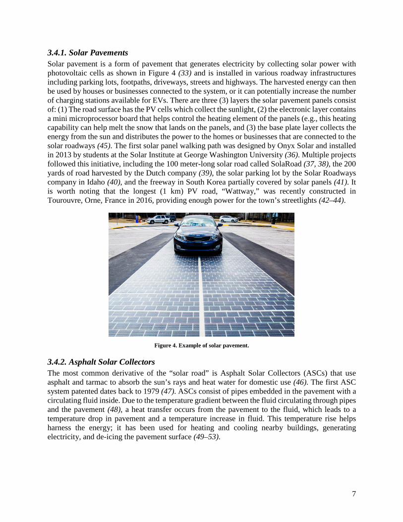
3.4.1. Solar Pavements Solar pavement is a form of pavement that generates electricity by collecting solar power with photovoltaic cells as shown in Figure 4 (33) and is installed in various roadway infrastructures including parking lots, footpaths, driveways, streets and highways. The harvested energy can then be used by houses or businesses connected to the system, or it can potentially increase the number of charging stations available for EVs. There are three (3) layers the solar pavement panels consist of: (1) The road surface has the PV cells which collect the sunlight, (2) the electronic layer contains a mini microprocessor board that helps control the heating element of the panels (e.g., this heating capability can help melt the snow that lands on the panels, and (3) the base plate layer collects the energy from the sun and distributes the power to the homes or businesses that are connected to the solar roadways (45). The first solar panel walking path was designed by Onyx Solar and installed in 2013 by students at the Solar Institute at George Washington University (36). Multiple projects followed this initiative, including the 100 meter-long solar road called SolaRoad (37, 38), the 200 yards of road harvested by the Dutch company (39), the solar parking lot by the Solar Roadways company in Idaho (40), and the freeway in South Korea partially covered by solar panels (41). It is worth noting that the longest (1 km) PV road, “Wattway,” was recently constructed in Tourouvre, Orne, France in 2016, providing enough power for the town’s streetlights (42–44).
Figure 4. Example of solar pavement.
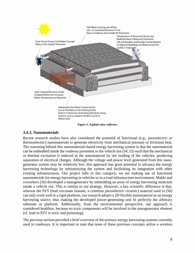
3.4.2. Asphalt Solar Collectors The most common derivative of the “solar road” is Asphalt Solar Collectors (ASCs) that use asphalt and tarmac to absorb the sun’s rays and heat water for domestic use (46). The first ASC system patented dates back to 1979 (47). ASCs consist of pipes embedded in the pavement with a circulating fluid inside. Due to the temperature gradient between the fluid circulating through pipes and the pavement (48), a heat transfer occurs from the pavement to the fluid, which leads to a temperature drop in pavement and a temperature increase in fluid. This temperature rise helps harness the energy; it has been used for heating and cooling nearby buildings, generating electricity, and de-icing the pavement surface (49–53).
8
Figure 5. Asphalt solar collector.
3.4.3. Nanomaterials Recent research studies have also considered the potential of functional (e.g., piezoelectric or thermoelectric) nanomaterials to generate electricity from mechanical pressure or frictional heat. The reasoning behind this nanomaterials-based energy harvesting system is that the nanomaterial can be embedded inside the roadway pavement or the vehicle tire (54, 55) such that the mechanical or thermal excitation is induced in the nanomaterial by tire loading of the vehicles, producing separation of electrical charges. Although the voltage and power level generated from this nano-generator system may be relatively low, this approach has great potential to advance the energy harvesting technology by miniaturizing the system and facilitating its integration with other existing infrastructures. Our project falls in this category; we are making use of functional nanomaterials for energy harvesting in vehicles or in a road infrastructure environment. Makki and coworkers (56) developed a nanogenerator by embedding an array of energy harvesting materials inside a vehicle tire. This is similar to our strategy. However, a key scientific difference is that, whereas the PZT (lead zirconate titanate, a common piezoelectric ceramic) material used in (56) can only work well in a rigid platform, our research adopts a 2D flexible nanomaterial as an energy harvesting source, thus making the developed power-generating unit fit perfectly the arbitrary substrate or platform. Additionally, from the environmental perspective, our approach is considered healthier, because no toxic components will be involved in the nanogenerator element (cf. lead in PZT is toxic and poisoning).
The previous section provided a brief overview of the primary energy harvesting systems currently used in roadways. It is important to note that none of these previous concepts utilize a wireless
9
charging method for electric vehicles. In our smart charging system, the emergent characteristics of the cutting-edge functional nanomaterials are coupled with efficient power conditioning and delivery circuits to recharge the vehicle battery; nanomaterials are used to power the embedded LEDs to transmit the harvested energy via light to the vehicle solar panel. Although this work focuses on embedding the piezoelectric nanomaterial inside the roadway pavements, it is worthwhile to note that the nanomaterial can be possibly placed inside the vehicle tire to further complement the LED-to-PV power transfer by exploiting both mechanical and thermal energies that exist in the vehicle tire/road interface. It will ultimately impact design of future roadways and vehicles, adapting to rapidly increasing needs for longer operational ranges of future vehicles for sustainable roadway environment.
3.5. Fiber Reinforced Polymer Modified Nanocomposite Overlay Fiber reinforced polymers (FRP) were introduced to the infrastructure industry by the late 20th century as materials capable of replacing regular steel reinforcing bars (57, 58). Since its introduction, FRP has been widely used in civil infrastructure to produce non-corroding structural elements (59) and to rehabilitate and strengthen existing concrete and steel elements in bridges and buildings. The widespread adoption of FRP is attributed to its lightweight, very high strength-to-weight ratio, and non-corrosive nature (60). Examples of FRP include (but are not limited to) carbon fiber reinforced polymer (CFRP), glass fiber reinforced polymer (GFRP), Aramid fiber reinforced polymer (AFRP), Basalt fiber reinforced polymer (BFRP) and others. While CFRP has shown the highest mechanical properties, it is the most expensive as well (60). Recently, researchers have extensively examined the use of nanomaterials to produce the next generation, low cost GFRPs with mechanical properties comparable to and better than CFRP (61–63). Moreover, in the last decade, there has been a strong outcry from transportation and safety engineers for the need for high friction surfacing materials to be used on top of current asphalt. Polymer overlays with broadcast bauxite aggregate have become the common high friction surfacing material adopted by the Federal Highway Administration (FHWA) (64). However, we note that for the purpose of this project, research on a polymer overlay material with superior flexibility and ability to incorporate nanomaterials has been very limited. This is very important because the nanomaterial will be placed on the roadway surface for energy harvesting, yet needs to be protected from harsh environmental or road conditions possibly by being embedded in a flexible polymer overlay. In (65) the ability to develop very flexible polymer overlays incorporating nanoparticles with superior ductility and unprecedented flexibility has been presented.
3.6. Power Conditioning Circuits for Nanomaterials Energy Harvesting Systems Power electronics circuits are key interfaces in energy harvesting systems. They should provide efficient rectification and storage of the incoming ac power while drawing as little quiescent current as possible (66). Additionally, smoothing, regulation, and level shifting of the output voltage may be required by the load electronics (67) because piezoelectric harvesters generate time-varying voltages. The load electronics require a regulated dc input voltage and therefore rectification is needed. There are two ways of performing rectification: passive and active. In the passive rectification, a full-wave rectifier circuit consisting of four diodes or transistor switches is commonly used (68–71). The main sources of power losses within full-wave diode rectifiers are typically the diodes’ forward voltage drops and the leakage currents when the devices are reverse

10
biased (72). Active or synchronous rectifier designs (73) are thus used to further increase the efficiency by reducing the conduction losses. However, the control circuitry of active topologies presents additional power consumption and may require conditioned supply (74, 75). Le and coworkers (76) demonstrated that power conversion efficiencies of the 80–90% range can be achieved with active rectification even at power levels as low as 20–30 μW, but still faced the challenge such as cold start, i.e., start up with no previously stored energy. One possible solution for that was suggested by using additional passive circuitry to bypass the active parts of the system during startup (77, 78).
As above-mentioned, the output voltage of the interface circuitry must comply with the requirements of the load electronics. This means that the voltage needs rectification, conversion, and regulation and this can be achieved by using either a single-stage AC/DC circuit or by combining separate rectification and DC/DC converter stages. Multiple circuit topologies have been presented in the literature for both the single-stage AC/DC conversion and the two-stage rectification with DC/DC conversion when used in energy harvesting systems. The various AC/DC conversion topologies have been suggested to include: (1) switched-capacitor converters (79–82), (2) passive (83, 84) and active voltage multipliers (85–88), (3) direct AC/DC switch mode converters (89–92), and (4) switched inductor converters (93–97) while for the DC/DC converters, such systems as DC/DC charge pumps (89, 99) and DC/DC switch-mode converters (100–102,106) have been used. In addition, since the maximum power needs to be extracted from the energy harvesting system, multiple maximum-power point tracking algorithms can be used to actively regulate the voltage and current operating point. It will ensure to maximize the instantaneous power extracted from the energy harvester.
11
4. METHODOLOGY The smart charging system developed in this work features the following three sequential pathways of energy conversion: (1) the mechanical energies available on the roadway are converted into electrical energies through the use of energy-harvestable 2D nanomaterials (EH2N), (2) these harvested energies are used (instead of the conventional power grid) to power the LEDs embedded in the roadway, and (3) the PV panels attached to the vehicle bottom finally convert the received light energy back to electricity.
4.1. Light Emitting Diodes (LEDs) and Photovoltaic (Solar) Panels In this project, the different solar panels and light emitting diodes (LEDs) technologies were surveyed as they serve as key elements in transmitting and receiving the light energy in the developed charging system.
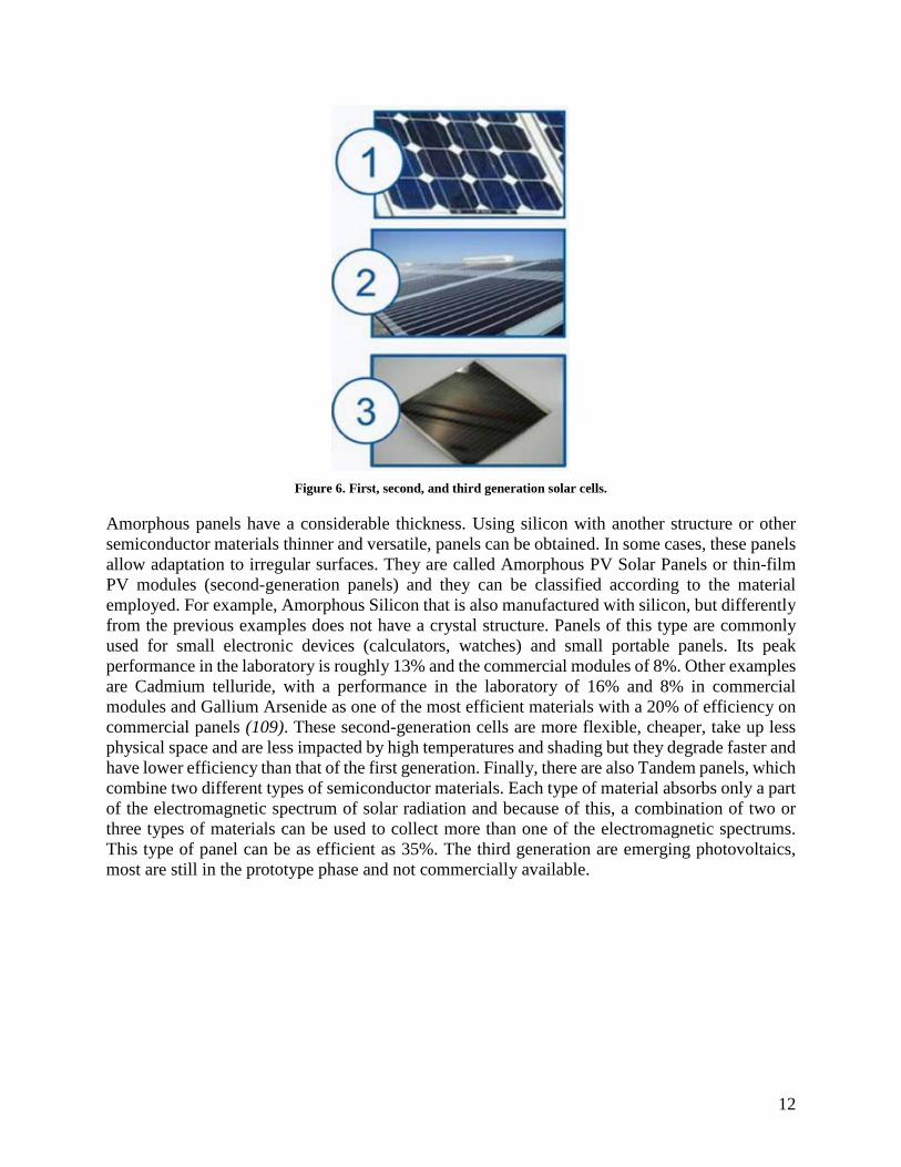
4.1.1. Photovoltaic Solar System The word “photovoltaic” comes from the Greek word “photo” meaning light and after Count Volta, the Italian physicist (1745-1827) whom the electrical unit Volt is named after. Photovoltaic technology began in 1839 with the French physicist Alexandre Becqueral’s discovery of the photo effect. In 1877, the first photovoltaic cell was constructed from Selenium. The photovoltaic effect was further explained by Albert Einstein and Robert Millikan in the early 1900s. Finally, in the 1950s, Shockley provided a model for the p-n junction, which enabled the beginning of modern photovoltaic technology development (107). In 1954 Bell Labs produced the first modern photovoltaic cell with an efficiency of only 4% (108). Early solar panels carried high price tags, usually costing a couple of thousand dollars per Watt. Energy generated at this cost was only feasible for space projects. Research in this arena progressively drove the costs lower and the efficiencies higher. In the last half century, photovoltaic technology has continued to improve, as has the economics of photovoltaic power generation.
There are varieties of solar panels based on semiconductor materials and manufacturing methods (Figure 6). The types of solar panels that can be found on the market based on the materials and manufactured process are: (1) monocrystalline panels, (2) polycrystalline panels, (3) amorphous panels and (4) tandem panels. Monocrystalline panels are called first generation and are made of sections of a silicon bar in one piece crystallized perfectly. The efficiency of these panels does not reach more than 24.7% in laboratory and 16% for commercial ones. The polycrystalline panels are similar to the previous type but in this case, the process of silicon crystallization is different. Polycrystalline panels are formed by pieces of a silicon bar that have been structured as disordered crystals. They are visually very recognizable because it presents a granulated surface. Lower efficiency than mono crystalline (19.8% laboratory and commercial modules 14%) is provided by these panels and consequently the price is lower.
12
Figure 6. First, second, and third generation solar cells.
Amorphous panels have a considerable thickness. Using silicon with another structure or other semiconductor materials thinner and versatile, panels can be obtained. In some cases, these panels allow adaptation to irregular surfaces. They are called Amorphous PV Solar Panels or thin-film PV modules (second-generation panels) and they can be classified according to the material employed. For example, Amorphous Silicon that is also manufactured with silicon, but differently from the previous examples does not have a crystal structure. Panels of this type are commonly used for small electronic devices (calculators, watches) and small portable panels. Its peak performance in the laboratory is roughly 13% and the commercial modules of 8%. Other examples are Cadmium telluride, with a performance in the laboratory of 16% and 8% in commercial modules and Gallium Arsenide as one of the most efficient materials with a 20% of efficiency on commercial panels (109). These second-generation cells are more flexible, cheaper, take up less physical space and are less impacted by high temperatures and shading but they degrade faster and have lower efficiency than that of the first generation. Finally, there are also Tandem panels, which combine two different types of semiconductor materials. Each type of material absorbs only a part of the electromagnetic spectrum of solar radiation and because of this, a combination of two or three types of materials can be used to collect more than one of the electromagnetic spectrums. This type of panel can be as efficient as 35%. The third generation are emerging photovoltaics, most are still in the prototype phase and not commercially available.

13
Table 1. Analysis of solar panels in the current market.
In Table 1, six different solar panels from five different companies were taken into consideration. The criteria that defined the solar panels were the power generation relative to the cost. The cost for the second generation relative to the power generation made it more feasible to look into first generation solar panels. The big disadvantage of first generation, in respect to this project application is the solar panels rigidness, this was counteracted by monocrystalline solar cells encased in ethylene vinyl acetate, ethylene tetrafluoroethylene and tedlar polyester tedlar, which is the culmination of using first generation solar cells and taking the inspiration of second generation solar cells flexibility. This takes the most efficient solar cells and adds the flexibility that makes for easier integration in the application of this project.
4.1.2. Light Emitting Diodes (LEDs) A light emitting diode (LED) is a semiconductor light source that emits light when current flows through it. LEDs have many advantages over incandescent light sources, including lower energy consumption, longer lifetime, improved physical robustness, smaller size, and faster switching. Light-emitting diodes are used in applications as diverse as aviation lighting, automotive headlamps, advertising, general lighting, traffic signals, camera flashes, lighted wallpaper and medical devices (102). For LEDs, the major criteria for choosing LEDs is their conversion measured as Lumens per Watt (lm/W) and flexibility which is used for durability as in this project LEDs are embedded into the nano-material. LEDs emit more lumens per watt than incandescent light bulbs (103). LEDs can have a relatively long useful life. One report estimates 35,000 to 50,000 hours of useful life, though time to complete failure may be shorter or longer (104). Fluorescent tubes typically are rated at about 10,000 to 25,000 hours, depending partly on the conditions of use, and incandescent light bulbs at 1,000 to 2,000 hours. Several US Department of Energy (DOE) demonstrations have shown that reduced maintenance costs from this extended lifetime, rather than energy savings, is the primary factor in determining the payback period for an LED product (105). There are four types of LEDs: Miniature LEDs, Red-Green-Blue (RGB) LEDs, LED strips and LED Tubes. Based on the current market approximately 200 Lumens/Watt is the maximum expected output.
Manufactuer Power Rating Vmp Iop Price Generation
EcoWorthy 10 W 17.3 V 0.58 A $21.16 First Renorgy 30 W 17.5 V 1.71 A $59.99 First SunKingdom 13 W 12.0 V 1.08 A $33.99 First + Second Zerodis 4.5 W 18.0 V 0.25 A $29.99 Second EcoWorthy 5.0 W 17.9 V 0.28 A $20.73 Second Lensun 20 W 18.0 V 1.11 A $79.00 First + Second
14
Table 2. Analysis of light emitting diodes in the current market.
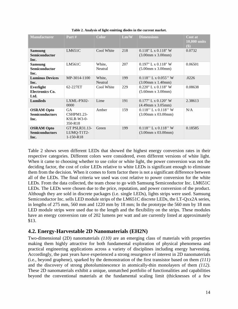
Manufacturer Part # Color Lm/W Dimensions Cost at 10,000 units ($)
Samsung Semiconductor Inc.
LM651C Cool White 218 0.118" L x 0.118" W (3.00mm x 3.00mm)
0.0732
Samsung Semiconductor Inc.
LM561C White, Neutral
207 0.197" L x 0.118" W (5.00mm x 3.00mm)
0.06501
Luminus Devices Inc.
MP-3014-1100 White, Neutral
199 0.118’’ L x 0.055’’ W (3.00mm x 1.40mm)
.0226
Everlight Electronics Co. Ltd.
62-227ET Cool White 229 0.220" L x 0.118" W (5.60mm x 3.00mm)
0.08638
Lumileds LXML-PX02-0000
Lime 191 0.177" L x 0.120" W (4.49mm x 3.05mm)
2.38613
OSRAM Opto Semiconductors Inc.
GA CSHPM1.23-KSLR-W3-0-350-R18
Amber 159 0.118’’ L x 0.118’’ W (3.00mm x 03.00mm)
N/A
OSRAM Opto Semiconductors Inc.
GT PSLR31.13-LUMQ-T1T2-1-150-R18
Green 199 0.118’’ L x 0.118’’ W (3.00mm x 03.00mm)
0.18585
Table 2 shows seven different LEDs that showed the highest energy conversion rates in their respective categories. Different colors were considered, even different versions of white light. When it came to choosing whether to use color or white light, the power conversion was not the deciding factor, the cost of color LEDs relative to white LEDs is significant enough to eliminate them from the decision. When it comes to form factor there is not a significant difference between all of the LEDs. The final criteria we used was cost relative to power conversion for the white LEDs. From the data collected, the team chose to go with Samsung Semiconductor Inc. LM651C LEDs. The LEDs were chosen due to the price, reputation, and power conversion of the product. Although they are sold in discrete packages (i.e. single LEDs), lights strips were used. Samsung Semiconductor Inc. sells LED module strips of the LM651C discrete LEDs, the LT-Qxx2A series, in lengths of 275 mm, 560 mm and 1220 mm by 18 mm; In the prototype the 560 mm by 18 mm LED module strips were used due to the length and the flexibility on the strips. These modules have an energy conversion rate of 202 lumens per watt and are currently listed at approximately $13.
4.2. Energy-Harvestable 2D Nanomaterials (EH2N) Two-dimensional (2D) nanomaterials (110) are an emerging class of materials with properties making them highly attractive for both fundamental exploration of physical phenomena and practical engineering applications across a variety of disciplines including energy harvesting. Accordingly, the past years have experienced a strong resurgence of interest in 2D nanomaterials (i.e., beyond graphene), sparked by the demonstration of the first transistor based on them (111) and the discovery of strong photoluminescence in atomically-thin monolayers of them (112). These 2D nanomaterials exhibit a unique, unmatched portfolio of functionalities and capabilities beyond the conventional materials at the fundamental scaling limit (thicknesses of a few
15
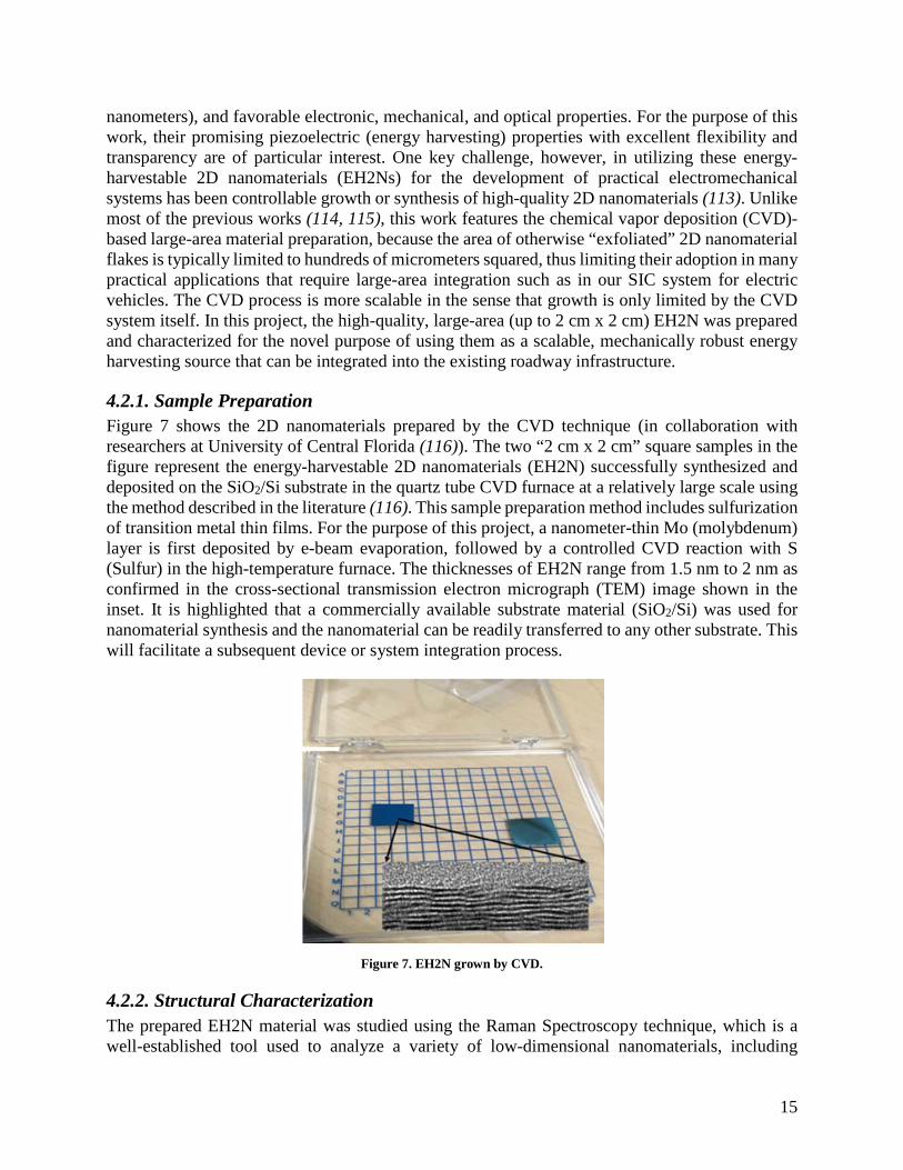
nanometers), and favorable electronic, mechanical, and optical properties. For the purpose of this work, their promising piezoelectric (energy harvesting) properties with excellent flexibility and transparency are of particular interest. One key challenge, however, in utilizing these energy-harvestable 2D nanomaterials (EH2Ns) for the development of practical electromechanical systems has been controllable growth or synthesis of high-quality 2D nanomaterials (113). Unlike most of the previous works (114, 115), this work features the chemical vapor deposition (CVD)-based large-area material preparation, because the area of otherwise “exfoliated” 2D nanomaterial flakes is typically limited to hundreds of micrometers squared, thus limiting their adoption in many practical applications that require large-area integration such as in our SIC system for electric vehicles. The CVD process is more scalable in the sense that growth is only limited by the CVD system itself. In this project, the high-quality, large-area (up to 2 cm x 2 cm) EH2N was prepared and characterized for the novel purpose of using them as a scalable, mechanically robust energy harvesting source that can be integrated into the existing roadway infrastructure.
4.2.1. Sample Preparation Figure 7 shows the 2D nanomaterials prepared by the CVD technique (in collaboration with researchers at University of Central Florida (116)). The two “2 cm x 2 cm” square samples in the figure represent the energy-harvestable 2D nanomaterials (EH2N) successfully synthesized and deposited on the SiO2/Si substrate in the quartz tube CVD furnace at a relatively large scale using the method described in the literature (116). This sample preparation method includes sulfurization of transition metal thin films. For the purpose of this project, a nanometer-thin Mo (molybdenum) layer is first deposited by e-beam evaporation, followed by a controlled CVD reaction with S (Sulfur) in the high-temperature furnace. The thicknesses of EH2N range from 1.5 nm to 2 nm as confirmed in the cross-sectional transmission electron micrograph (TEM) image shown in the inset. It is highlighted that a commercially available substrate material (SiO2/Si) was used for nanomaterial synthesis and the nanomaterial can be readily transferred to any other substrate. This will facilitate a subsequent device or system integration process.
Figure 7. EH2N grown by CVD.
4.2.2. Structural Characterization The prepared EH2N material was studied using the Raman Spectroscopy technique, which is a well-established tool used to analyze a variety of low-dimensional nanomaterials, including
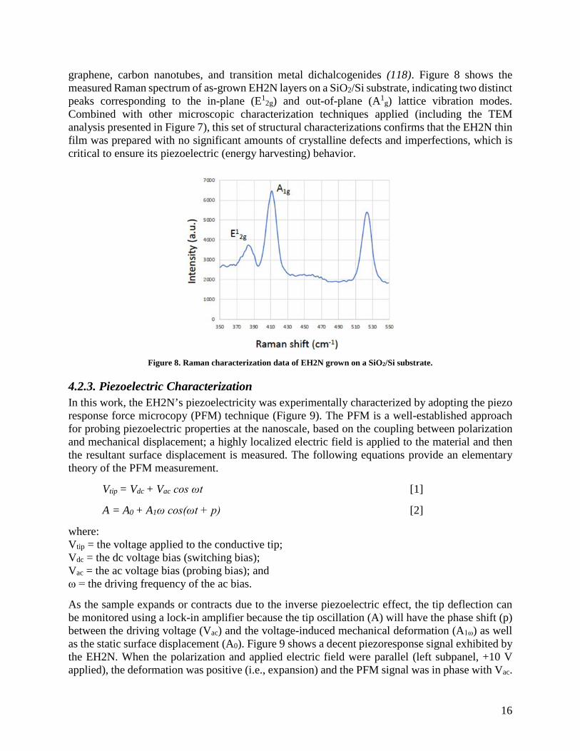
16
graphene, carbon nanotubes, and transition metal dichalcogenides (118). Figure 8 shows the measured Raman spectrum of as-grown EH2N layers on a SiO2/Si substrate, indicating two distinct peaks corresponding to the in-plane (E1
2g) and out-of-plane (A1g) lattice vibration modes.
Combined with other microscopic characterization techniques applied (including the TEM analysis presented in Figure 7), this set of structural characterizations confirms that the EH2N thin film was prepared with no significant amounts of crystalline defects and imperfections, which is critical to ensure its piezoelectric (energy harvesting) behavior.
Figure 8. Raman characterization data of EH2N grown on a SiO2/Si substrate.
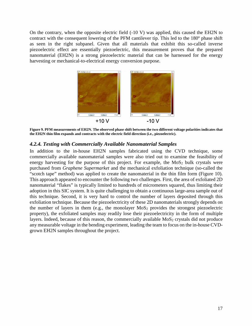
4.2.3. Piezoelectric Characterization In this work, the EH2N’s piezoelectricity was experimentally characterized by adopting the piezo response force microcopy (PFM) technique (Figure 9). The PFM is a well-established approach for probing piezoelectric properties at the nanoscale, based on the coupling between polarization and mechanical displacement; a highly localized electric field is applied to the material and then the resultant surface displacement is measured. The following equations provide an elementary theory of the PFM measurement.
Vtip = Vdc + Vac cos ωt [1]
A = A0 + A1ω cos(ωt + p) [2]
where: Vtip = the voltage applied to the conductive tip; Vdc = the dc voltage bias (switching bias); Vac = the ac voltage bias (probing bias); and ω = the driving frequency of the ac bias.
As the sample expands or contracts due to the inverse piezoelectric effect, the tip deflection can be monitored using a lock-in amplifier because the tip oscillation (A) will have the phase shift (p) between the driving voltage (Vac) and the voltage-induced mechanical deformation (A1ω) as well as the static surface displacement (A0). Figure 9 shows a decent piezoresponse signal exhibited by the EH2N. When the polarization and applied electric field were parallel (left subpanel, +10 V applied), the deformation was positive (i.e., expansion) and the PFM signal was in phase with Vac.
17
On the contrary, when the opposite electric field (-10 V) was applied, this caused the EH2N to contract with the consequent lowering of the PFM cantilever tip. This led to the 180º phase shift as seen in the right subpanel. Given that all materials that exhibit this so-called inverse piezoelectric effect are essentially piezoelectric, this measurement proves that the prepared nanomaterial (EH2N) is a strong piezoelectric material that can be harnessed for the energy harvesting or mechanical-to-electrical energy conversion purpose.
Figure 9. PFM measurements of EH2N. The observed phase shift between the two different voltage polarities indicates that the EH2N thin film expands and contracts with the electric field direction (i.e., piezoelectric).
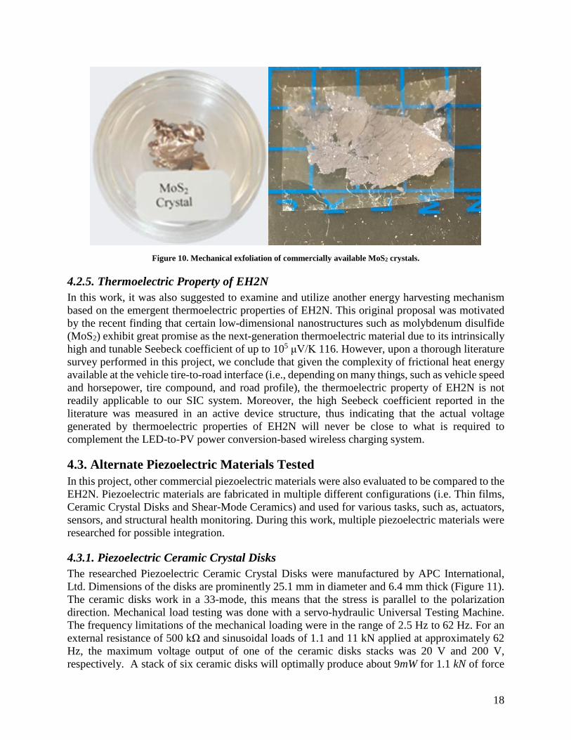
4.2.4. Testing with Commercially Available Nanomaterial Samples In addition to the in-house EH2N samples fabricated using the CVD technique, some commercially available nanomaterial samples were also tried out to examine the feasibility of energy harvesting for the purpose of this project. For example, the MoS2 bulk crystals were purchased from Graphene Supermarket and the mechanical exfoliation technique (so-called the “scotch tape” method) was applied to create the nanomaterial in the thin film form (Figure 10). This approach appeared to encounter the following two challenges. First, the area of exfoliated 2D nanomaterial “flakes” is typically limited to hundreds of micrometers squared, thus limiting their adoption in this SIC system. It is quite challenging to obtain a continuous large-area sample out of this technique. Second, it is very hard to control the number of layers deposited through this exfoliation technique. Because the piezoelectricity of these 2D nanomaterials strongly depends on the number of layers in them (e.g., the monolayer MoS2 provides the strongest piezoelectric property), the exfoliated samples may readily lose their piezoelectricity in the form of multiple layers. Indeed, because of this reason, the commercially available MoS2 crystals did not produce any measurable voltage in the bending experiment, leading the team to focus on the in-house CVD-grown EH2N samples throughout the project.
18
Figure 10. Mechanical exfoliation of commercially available MoS2 crystals.
4.2.5. Thermoelectric Property of EH2N In this work, it was also suggested to examine and utilize another energy harvesting mechanism based on the emergent thermoelectric properties of EH2N. This original proposal was motivated by the recent finding that certain low-dimensional nanostructures such as molybdenum disulfide (MoS2) exhibit great promise as the next-generation thermoelectric material due to its intrinsically high and tunable Seebeck coefficient of up to 105 μV/K 116. However, upon a thorough literature survey performed in this project, we conclude that given the complexity of frictional heat energy available at the vehicle tire-to-road interface (i.e., depending on many things, such as vehicle speed and horsepower, tire compound, and road profile), the thermoelectric property of EH2N is not readily applicable to our SIC system. Moreover, the high Seebeck coefficient reported in the literature was measured in an active device structure, thus indicating that the actual voltage generated by thermoelectric properties of EH2N will never be close to what is required to complement the LED-to-PV power conversion-based wireless charging system.
4.3. Alternate Piezoelectric Materials Tested In this project, other commercial piezoelectric materials were also evaluated to be compared to the EH2N. Piezoelectric materials are fabricated in multiple different configurations (i.e. Thin films, Ceramic Crystal Disks and Shear-Mode Ceramics) and used for various tasks, such as, actuators, sensors, and structural health monitoring. During this work, multiple piezoelectric materials were researched for possible integration.
4.3.1. Piezoelectric Ceramic Crystal Disks The researched Piezoelectric Ceramic Crystal Disks were manufactured by APC International, Ltd. Dimensions of the disks are prominently 25.1 mm in diameter and 6.4 mm thick (Figure 11). The ceramic disks work in a 33-mode, this means that the stress is parallel to the polarization direction. Mechanical load testing was done with a servo-hydraulic Universal Testing Machine. The frequency limitations of the mechanical loading were in the range of 2.5 Hz to 62 Hz. For an external resistance of 500 kΩ and sinusoidal loads of 1.1 and 11 kN applied at approximately 62 Hz, the maximum voltage output of one of the ceramic disks stacks was 20 V and 200 V, respectively. A stack of six ceramic disks will optimally produce about 9mW for 1.1 kN of force
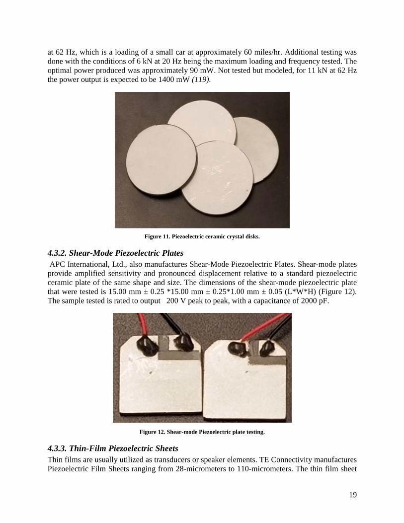
19
at 62 Hz, which is a loading of a small car at approximately 60 miles/hr. Additional testing was done with the conditions of 6 kN at 20 Hz being the maximum loading and frequency tested. The optimal power produced was approximately 90 mW. Not tested but modeled, for 11 kN at 62 Hz the power output is expected to be 1400 mW (119).
Figure 11. Piezoelectric ceramic crystal disks.
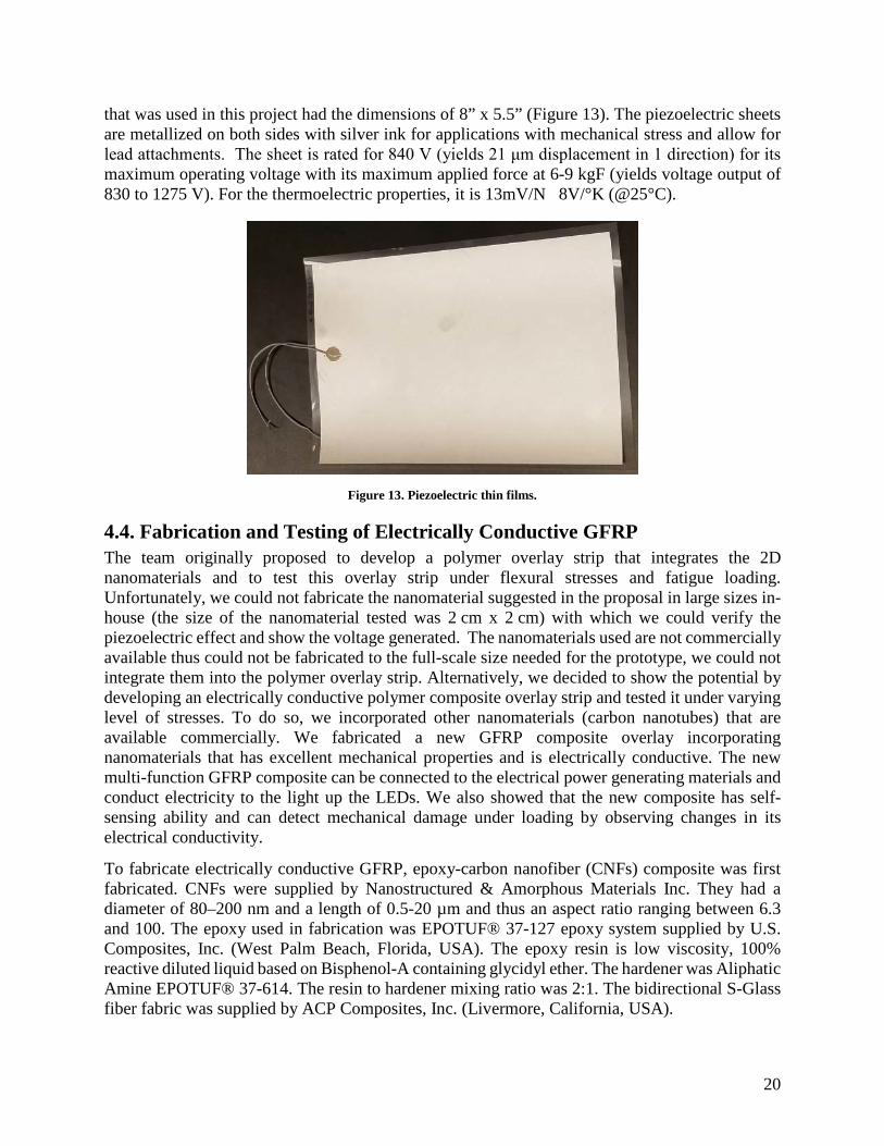
4.3.2. Shear-Mode Piezoelectric Plates APC International, Ltd., also manufactures Shear-Mode Piezoelectric Plates. Shear-mode plates provide amplified sensitivity and pronounced displacement relative to a standard piezoelectric ceramic plate of the same shape and size. The dimensions of the shear-mode piezoelectric plate that were tested is 15.00 mm ± 0.25 *15.00 mm ± 0.25*1.00 mm ± 0.05 (L*W*H) (Figure 12). The sample tested is rated to output 200 V peak to peak, with a capacitance of 2000 pF.
Figure 12. Shear-mode Piezoelectric plate testing.
4.3.3. Thin-Film Piezoelectric Sheets Thin films are usually utilized as transducers or speaker elements. TE Connectivity manufactures Piezoelectric Film Sheets ranging from 28-micrometers to 110-micrometers. The thin film sheet
20
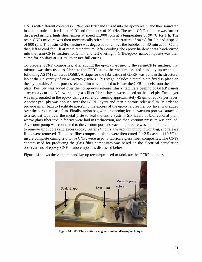
that was used in this project had the dimensions of 8” x 5.5” (Figure 13). The piezoelectric sheets are metallized on both sides with silver ink for applications with mechanical stress and allow for lead attachments. The sheet is rated for 840 V (yields 21 μm displacement in 1 direction) for its maximum operating voltage with its maximum applied force at 6-9 kgF (yields voltage output of 830 to 1275 V). For the thermoelectric properties, it is 13mV/N 8V/°K (@25°C).
Figure 13. Piezoelectric thin films.
4.4. Fabrication and Testing of Electrically Conductive GFRP The team originally proposed to develop a polymer overlay strip that integrates the 2D nanomaterials and to test this overlay strip under flexural stresses and fatigue loading. Unfortunately, we could not fabricate the nanomaterial suggested in the proposal in large sizes in-house (the size of the nanomaterial tested was 2 cm x 2 cm) with which we could verify the piezoelectric effect and show the voltage generated. The nanomaterials used are not commercially available thus could not be fabricated to the full-scale size needed for the prototype, we could not integrate them into the polymer overlay strip. Alternatively, we decided to show the potential by developing an electrically conductive polymer composite overlay strip and tested it under varying level of stresses. To do so, we incorporated other nanomaterials (carbon nanotubes) that are available commercially. We fabricated a new GFRP composite overlay incorporating nanomaterials that has excellent mechanical properties and is electrically conductive. The new multi-function GFRP composite can be connected to the electrical power generating materials and conduct electricity to the light up the LEDs. We also showed that the new composite has self-sensing ability and can detect mechanical damage under loading by observing changes in its electrical conductivity.
To fabricate electrically conductive GFRP, epoxy-carbon nanofiber (CNFs) composite was first fabricated. CNFs were supplied by Nanostructured & Amorphous Materials Inc. They had a diameter of 80–200 nm and a length of 0.5-20 µm and thus an aspect ratio ranging between 6.3 and 100. The epoxy used in fabrication was EPOTUF® 37-127 epoxy system supplied by U.S. Composites, Inc. (West Palm Beach, Florida, USA). The epoxy resin is low viscosity, 100% reactive diluted liquid based on Bisphenol-A containing glycidyl ether. The hardener was Aliphatic Amine EPOTUF® 37-614. The resin to hardener mixing ratio was 2:1. The bidirectional S-Glass fiber fabric was supplied by ACP Composites, Inc. (Livermore, California, USA).
21
CNFs with different contents (2.0 %) were firsthand stirred into the epoxy resin, and then sonicated in a path sonicator for 1 h at 40 °C and frequency of 40 kHz. The resin-CNFs mixture was further dispersed using a high shear mixer at speed 11,000 rpm at a temperature of 90 °C for 1 h. The resin-CNFs mixture was then mechanically stirred at a temperature of 90 °C for 2 h and a speed of 800 rpm. The resin-CNFs mixture was degassed to remove the bubbles for 30 min at 50 °C and then left to cool for 1 h at room temperature. After cooling, the epoxy hardener was hand-stirred into the resin-CNFs mixture for 5 min and left overnight. CNFs/epoxy nanocomposite was then cured for 2.5 days at 110 °C to ensure full curing.
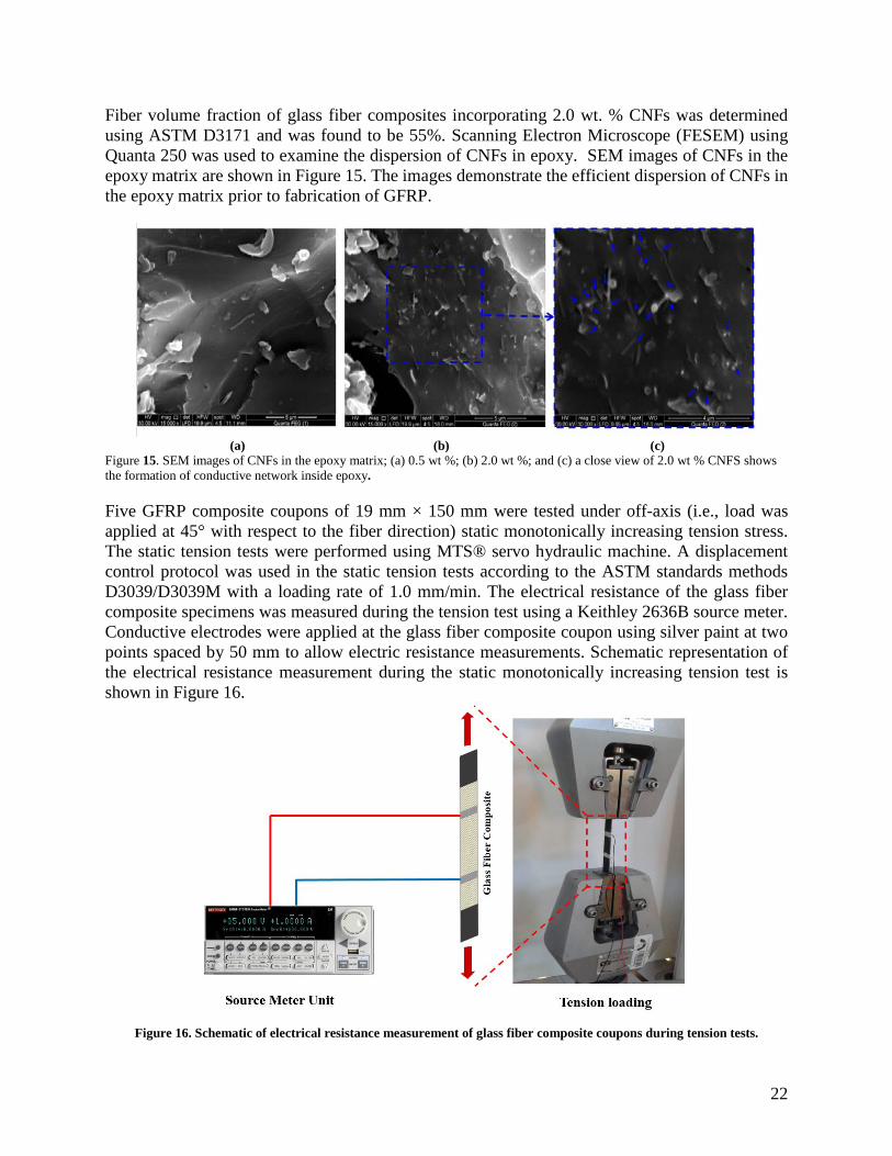
To prepare GFRP composites, after adding the epoxy hardener to the resin-CNFs mixture, that mixture was then used to fabricate the GFRP using the vacuum assisted hand lay-up technique following ASTM standards D5687. A stage for the fabrication of GFRP was built in the structural lab at the University of New Mexico (UNM). This stage includes a metal plate fixed in place on the lay-up table. A non-porous release film was attached to isolate the GFRP panels from the metal plate. Peel ply was added over the non-porous release film to facilitate peeling of GFRP panels after epoxy curing. Afterward, the glass fiber fabrics layers were placed on the peel ply. Each layer was impregnated in the epoxy using a roller consuming approximately 45 gm of epoxy per layer. Another peel ply was applied over the GFRP layers and then a porous release film. In order to provide an air bath to facilitate absorbing the excess of the epoxy, a breather ply layer was added over the porous release film. Finally, nylon bag with an opening for the vacuum port was attached to a sealant tape over the metal plate to seal the entire system. Six layers of bidirectional plain weave glass fiber textile fabrics were laid in 0° direction, and then vacuum pressure was applied. A vacuum pump was connected to the vacuum port and vacuum pressure was applied for 24 hours to remove air bubbles and excess epoxy. After 24 hours, the vacuum pump, nylon bag, and release films were removed. The glass fiber composite plates were then cured for 2.5 days at 110 °C to insure complete curing. 2.0 wt % CNFs were used to fabricate glass fiber composites. The CNFs content used for producing the glass fiber composites was based on the electrical percolation observations of epoxy-CNFs nanocomposites discussed below.
Figure 14 shows the vacuum hand lay-up technique used to fabricate the GFRP coupons.
Figure 14. GFRP fabrication using vacuum hand lay-up technique.
22
Fiber volume fraction of glass fiber composites incorporating 2.0 wt. % CNFs was determined using ASTM D3171 and was found to be 55%. Scanning Electron Microscope (FESEM) using Quanta 250 was used to examine the dispersion of CNFs in epoxy. SEM images of CNFs in the epoxy matrix are shown in Figure 15. The images demonstrate the efficient dispersion of CNFs in the epoxy matrix prior to fabrication of GFRP.
(a) (b) (c) Figure 15. SEM images of CNFs in the epoxy matrix; (a) 0.5 wt %; (b) 2.0 wt %; and (c) a close view of 2.0 wt % CNFS shows the formation of conductive network inside epoxy.
Five GFRP composite coupons of 19 mm × 150 mm were tested under off-axis (i.e., load was applied at 45° with respect to the fiber direction) static monotonically increasing tension stress. The static tension tests were performed using MTS® servo hydraulic machine. A displacement control protocol was used in the static tension tests according to the ASTM standards methods D3039/D3039M with a loading rate of 1.0 mm/min. The electrical resistance of the glass fiber composite specimens was measured during the tension test using a Keithley 2636B source meter. Conductive electrodes were applied at the glass fiber composite coupon using silver paint at two points spaced by 50 mm to allow electric resistance measurements. Schematic representation of the electrical resistance measurement during the static monotonically increasing tension test is shown in Figure 16.
Figure 16. Schematic of electrical resistance measurement of glass fiber composite coupons during tension tests.
23
Damage in glass fiber composite coupons was estimated in terms of the change of the electrical conductivity during loading. The electrical conductivity was measured and a metric of damage based on electrical conductivity change denoted DE(t) was calculated using Equation 3.
𝐷𝐷𝐸𝐸(𝑡𝑡) = 1 − σ(𝑡𝑡)σ(𝑡𝑡0) % [3]
where: DE(t) = the electrical damage measured at time t; σ(t0) = the initial electrical conductivity of the composite prior to load application at time t0; and σ(t) = the electrical conductivity of the composite at time t.
Moreover, a metric of damage based on the change of modulus of elasticity, representing mechanical damage and denoted DM(t) was calculated using Equation 4:
𝐷𝐷𝑀𝑀(𝑡𝑡) = 1 − 𝐸𝐸(𝑡𝑡)𝐸𝐸(𝑡𝑡0) % [4]
where E(t0) is the initial tangent modulus of elasticity of the glass fiber composite coupon at t0 and E(t) is the tangent modulus of elasticity of the glass fiber composite coupon at time t. A minimum tangent modulus of zero was assumed to account for the descending stress-strain.
4.5. Power Delivery Circuit Design In this section, we developed the power circuits that are needed for developing the lab-scale proof-of-concept. Since the nanomaterials were not fabricated in large scale that would fit the prototype, a power conditioning circuit for road-embedded nanomaterials was not needed at this stage. Section 5.4 discusses the recommended power conditioning circuit for the field implementation and represents the circuit diagram in Matlab/Simulink of the suggested circuits. However, in this section, the team developed the power conditioning circuit that converts the received light energy in the PV panels back to electricity and charges a battery representing the vehicle battery.
Figure 17 is an image of the synchronous, switch-mode, battery charge control that was used to implement maximum power point tracking (MPPT). MPPT is an algorithm that is utilized in charge controllers to extract the maximum power from a photo-voltaic (PV) module. The voltage that a PV module is at the maximum power is called the peak power voltage that is typically found within the datasheet of a PV module. This peak power voltage is typically between 17-18 volts (for our prototypes) and referred to as Vmp or Vop meaning maximum power voltage or optimal power voltage, respectively. To implement this, the bq24650EVM evaluation module was used; the module takes the input from the solar panel array into the J1 connection on the left side of the board and regulates the voltage to the programable maximum power voltage. The maximum power is then outputted to the right side of the board where there are two loads, the first load is the system denoted by Vsys and the second load is the charger output denoted by Vout. In the large-scale application, the system can be anything that we want to power, such as, actuators or sensors and the second load is a battery, this can be the EV battery or any other battery in the range of 2.1 to 26 volts. For the scaled down version, a resistive load is used to calculate the power outputted from Vsys and for Vout a 12-volt lead-acid battery is connected.
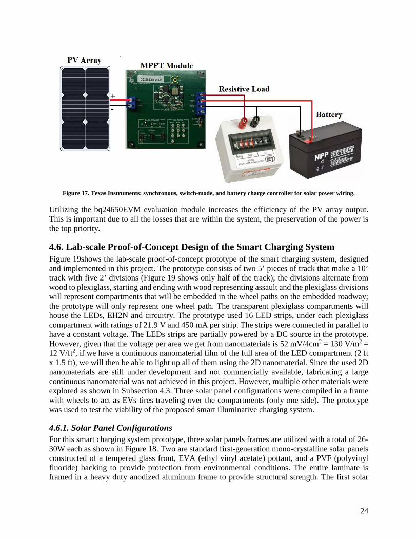
24
Figure 17. Texas Instruments: synchronous, switch-mode, and battery charge controller for solar power wiring.
Utilizing the bq24650EVM evaluation module increases the efficiency of the PV array output. This is important due to all the losses that are within the system, the preservation of the power is the top priority.
4.6. Lab-scale Proof-of-Concept Design of the Smart Charging System Figure 19shows the lab-scale proof-of-concept prototype of the smart charging system, designed and implemented in this project. The prototype consists of two 5’ pieces of track that make a 10’ track with five 2’ divisions (Figure 19 shows only half of the track); the divisions alternate from wood to plexiglass, starting and ending with wood representing assault and the plexiglass divisions will represent compartments that will be embedded in the wheel paths on the embedded roadway; the prototype will only represent one wheel path. The transparent plexiglass compartments will house the LEDs, EH2N and circuitry. The prototype used 16 LED strips, under each plexiglass compartment with ratings of 21.9 V and 450 mA per strip. The strips were connected in parallel to have a constant voltage. The LEDs strips are partially powered by a DC source in the prototype. However, given that the voltage per area we get from nanomaterials is 52 mV/4cm2 = 130 V/m2 = 12 V/ft2, if we have a continuous nanomaterial film of the full area of the LED compartment (2 ft x 1.5 ft), we will then be able to light up all of them using the 2D nanomaterial. Since the used 2D nanomaterials are still under development and not commercially available, fabricating a large continuous nanomaterial was not achieved in this project. However, multiple other materials were explored as shown in Subsection 4.3. Three solar panel configurations were compiled in a frame with wheels to act as EVs tires traveling over the compartments (only one side). The prototype was used to test the viability of the proposed smart illuminative charging system.
4.6.1. Solar Panel Configurations For this smart charging system prototype, three solar panels frames are utilized with a total of 26-30W each as shown in Figure 18. Two are standard first-generation mono-crystalline solar panels constructed of a tempered glass front, EVA (ethyl vinyl acetate) pottant, and a PVF (polyvinyl fluoride) backing to provide protection from environmental conditions. The entire laminate is framed in a heavy duty anodized aluminum frame to provide structural strength. The first solar
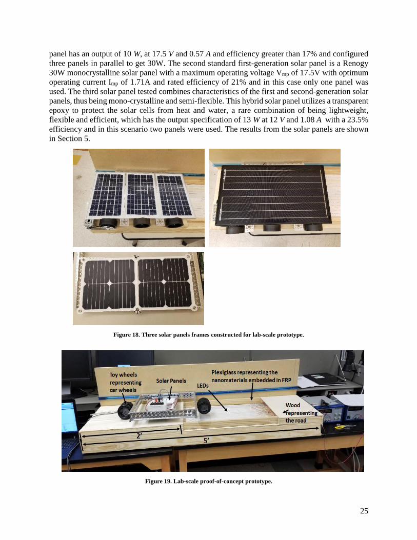
25
panel has an output of 10 W, at 17.5 V and 0.57 A and efficiency greater than 17% and configured three panels in parallel to get 30W. The second standard first-generation solar panel is a Renogy 30W monocrystalline solar panel with a maximum operating voltage Vmp of 17.5V with optimum operating current Imp of 1.71A and rated efficiency of 21% and in this case only one panel was used. The third solar panel tested combines characteristics of the first and second-generation solar panels, thus being mono-crystalline and semi-flexible. This hybrid solar panel utilizes a transparent epoxy to protect the solar cells from heat and water, a rare combination of being lightweight, flexible and efficient, which has the output specification of 13 W at 12 V and 1.08 A with a 23.5% efficiency and in this scenario two panels were used. The results from the solar panels are shown in Section 5.
Figure 18. Three solar panels frames constructed for lab-scale prototype.
Figure 19. Lab-scale proof-of-concept prototype.
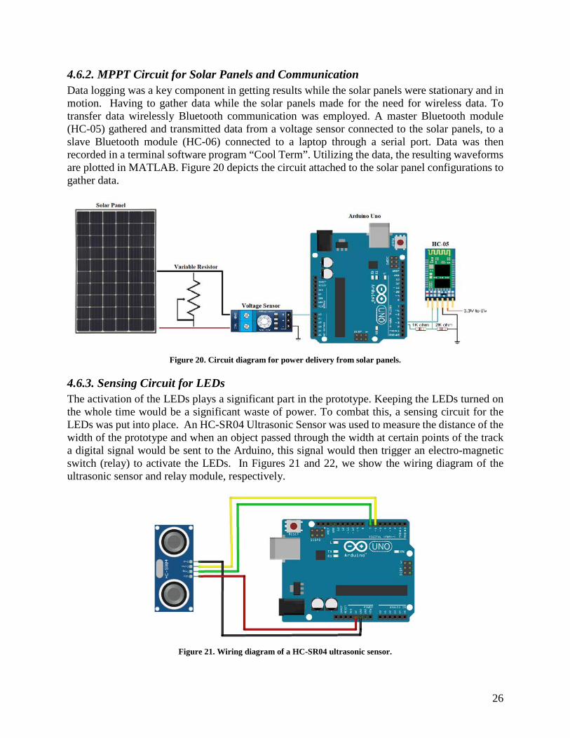
26
4.6.2. MPPT Circuit for Solar Panels and Communication Data logging was a key component in getting results while the solar panels were stationary and in motion. Having to gather data while the solar panels made for the need for wireless data. To transfer data wirelessly Bluetooth communication was employed. A master Bluetooth module (HC-05) gathered and transmitted data from a voltage sensor connected to the solar panels, to a slave Bluetooth module (HC-06) connected to a laptop through a serial port. Data was then recorded in a terminal software program “Cool Term”. Utilizing the data, the resulting waveforms are plotted in MATLAB. Figure 20 depicts the circuit attached to the solar panel configurations to gather data.
Figure 20. Circuit diagram for power delivery from solar panels.
4.6.3. Sensing Circuit for LEDs The activation of the LEDs plays a significant part in the prototype. Keeping the LEDs turned on the whole time would be a significant waste of power. To combat this, a sensing circuit for the LEDs was put into place. An HC-SR04 Ultrasonic Sensor was used to measure the distance of the width of the prototype and when an object passed through the width at certain points of the track a digital signal would be sent to the Arduino, this signal would then trigger an electro-magnetic switch (relay) to activate the LEDs. In Figures 21 and 22, we show the wiring diagram of the ultrasonic sensor and relay module, respectively.
Figure 21. Wiring diagram of a HC-SR04 ultrasonic sensor.
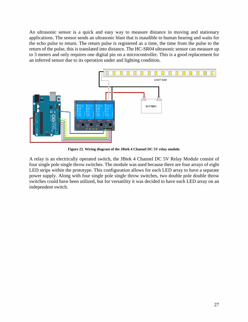
27
An ultrasonic sensor is a quick and easy way to measure distance in moving and stationary applications. The sensor sends an ultrasonic blast that is inaudible to human hearing and waits for the echo pulse to return. The return pulse is registered as a time, the time from the pulse to the return of the pulse, this is translated into distance. The HC-SR04 ultrasonic sensor can measure up to 3 meters and only requires one digital pin on a microcontroller. This is a good replacement for an inferred sensor due to its operation under and lighting condition.
Figure 22. Wiring diagram of the JBtek 4 Channel DC 5V relay module.
A relay is an electrically operated switch, the JBtek 4 Channel DC 5V Relay Module consist of four single pole single throw switches. The module was used because there are four arrays of eight LED strips within the prototype. This configuration allows for each LED array to have a separate power supply. Along with four single pole single throw switches, two double pole double throw switches could have been utilized, but for versatility it was decided to have each LED array on an independent switch.
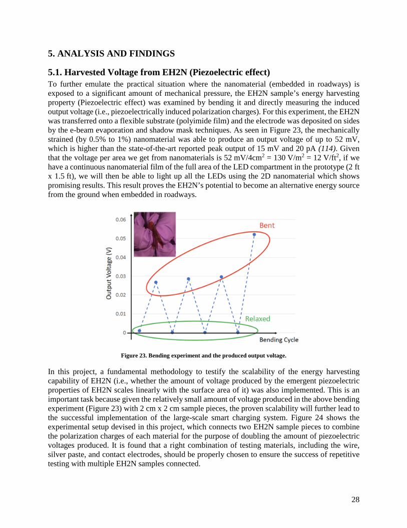
28
5. ANALYSIS AND FINDINGS
5.1. Harvested Voltage from EH2N (Piezoelectric effect) To further emulate the practical situation where the nanomaterial (embedded in roadways) is exposed to a significant amount of mechanical pressure, the EH2N sample’s energy harvesting property (Piezoelectric effect) was examined by bending it and directly measuring the induced output voltage (i.e., piezoelectrically induced polarization charges). For this experiment, the EH2N was transferred onto a flexible substrate (polyimide film) and the electrode was deposited on sides by the e-beam evaporation and shadow mask techniques. As seen in Figure 23, the mechanically strained (by 0.5% to 1%) nanomaterial was able to produce an output voltage of up to 52 mV, which is higher than the state-of-the-art reported peak output of 15 mV and 20 pA (114). Given that the voltage per area we get from nanomaterials is 52 mV/4cm2 = 130 V/m2 = 12 V/ft2, if we have a continuous nanomaterial film of the full area of the LED compartment in the prototype (2 ft x 1.5 ft), we will then be able to light up all the LEDs using the 2D nanomaterial which shows promising results. This result proves the EH2N’s potential to become an alternative energy source from the ground when embedded in roadways.
Figure 23. Bending experiment and the produced output voltage.
In this project, a fundamental methodology to testify the scalability of the energy harvesting capability of EH2N (i.e., whether the amount of voltage produced by the emergent piezoelectric properties of EH2N scales linearly with the surface area of it) was also implemented. This is an important task because given the relatively small amount of voltage produced in the above bending experiment (Figure 23) with 2 cm x 2 cm sample pieces, the proven scalability will further lead to the successful implementation of the large-scale smart charging system. Figure 24 shows the experimental setup devised in this project, which connects two EH2N sample pieces to combine the polarization charges of each material for the purpose of doubling the amount of piezoelectric voltages produced. It is found that a right combination of testing materials, including the wire, silver paste, and contact electrodes, should be properly chosen to ensure the success of repetitive testing with multiple EH2N samples connected.
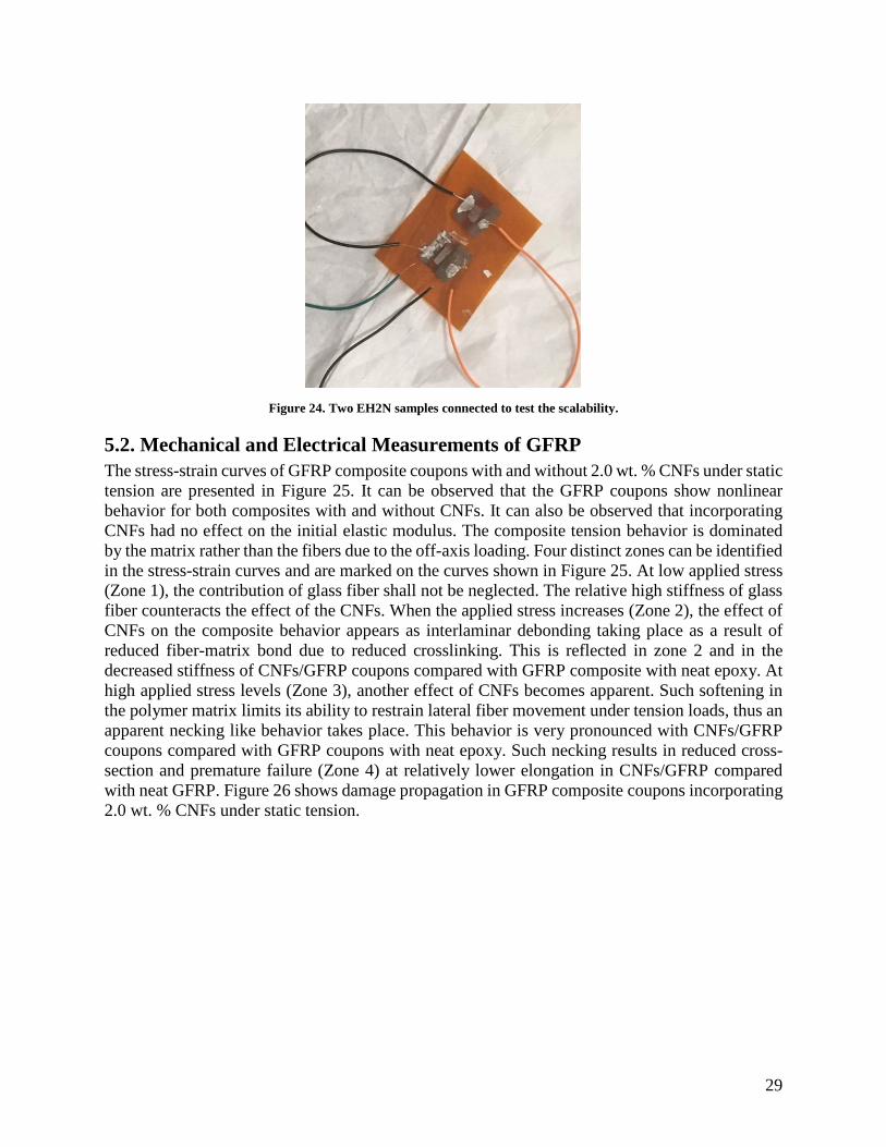
29
Figure 24. Two EH2N samples connected to test the scalability.
5.2. Mechanical and Electrical Measurements of GFRP The stress-strain curves of GFRP composite coupons with and without 2.0 wt. % CNFs under static tension are presented in Figure 25. It can be observed that the GFRP coupons show nonlinear behavior for both composites with and without CNFs. It can also be observed that incorporating CNFs had no effect on the initial elastic modulus. The composite tension behavior is dominated by the matrix rather than the fibers due to the off-axis loading. Four distinct zones can be identified in the stress-strain curves and are marked on the curves shown in Figure 25. At low applied stress (Zone 1), the contribution of glass fiber shall not be neglected. The relative high stiffness of glass fiber counteracts the effect of the CNFs. When the applied stress increases (Zone 2), the effect of CNFs on the composite behavior appears as interlaminar debonding taking place as a result of reduced fiber-matrix bond due to reduced crosslinking. This is reflected in zone 2 and in the decreased stiffness of CNFs/GFRP coupons compared with GFRP composite with neat epoxy. At high applied stress levels (Zone 3), another effect of CNFs becomes apparent. Such softening in the polymer matrix limits its ability to restrain lateral fiber movement under tension loads, thus an apparent necking like behavior takes place. This behavior is very pronounced with CNFs/GFRP coupons compared with GFRP coupons with neat epoxy. Such necking results in reduced cross-section and premature failure (Zone 4) at relatively lower elongation in CNFs/GFRP compared with neat GFRP. Figure 26 shows damage propagation in GFRP composite coupons incorporating 2.0 wt. % CNFs under static tension.
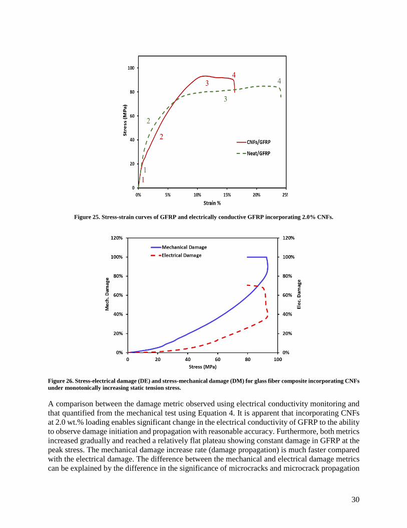
30
Figure 25. Stress-strain curves of GFRP and electrically conductive GFRP incorporating 2.0% CNFs.
Figure 26. Stress-electrical damage (DE) and stress-mechanical damage (DM) for glass fiber composite incorporating CNFs under monotonically increasing static tension stress.
A comparison between the damage metric observed using electrical conductivity monitoring and that quantified from the mechanical test using Equation 4. It is apparent that incorporating CNFs at 2.0 wt.% loading enables significant change in the electrical conductivity of GFRP to the ability to observe damage initiation and propagation with reasonable accuracy. Furthermore, both metrics increased gradually and reached a relatively flat plateau showing constant damage in GFRP at the peak stress. The mechanical damage increase rate (damage propagation) is much faster compared with the electrical damage. The difference between the mechanical and electrical damage metrics can be explained by the difference in the significance of microcracks and microcrack propagation
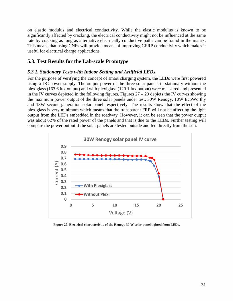
31
on elastic modulus and electrical conductivity. While the elastic modulus is known to be significantly affected by cracking, the electrical conductivity might not be influenced at the same rate by cracking as long as alternative electrically conductive paths can be found in the matrix. This means that using CNFs will provide means of improving GFRP conductivity which makes it useful for electrical charge applications.
5.3. Test Results for the Lab-scale Prototype
5.3.1. Stationary Tests with Indoor Setting and Artificial LEDs For the purpose of verifying the concept of smart charging system, the LEDs were first powered using a DC power supply. The output power of the three solar panels in stationary without the plexiglass (163.6 lux output) and with plexiglass (120.1 lux output) were measured and presented in the IV curves depicted in the following figures. Figures 27 – 29 depicts the IV curves showing the maximum power output of the three solar panels under test, 30W Renogy, 10W EcoWorthy and 13W second-generation solar panel respectively. The results show that the effect of the plexiglass is very minimum which means that the transparent FRP will not be affecting the light output from the LEDs embedded in the roadway. However, it can be seen that the power output was about 62% of the rated power of the panels and that is due to the LEDs. Further testing will compare the power output if the solar panels are tested outside and fed directly from the sun.
Figure 27. Electrical characteristic of the Renogy 30 W solar panel lighted from LEDs.
00.10.20.30.40.50.60.70.80.9
0 5 10 15 20 25
Curr
ent (
A)
Voltage (V)
30W Renogy solar panel IV curve
With Plexiglass
Without Plexi
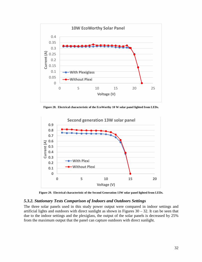
32
Figure 28. Electrical characteristic of the EcoWorthy 10 W solar panel lighted from LEDs.
Figure 29. Electrical characteristic of the Second Generation 13W solar panel lighted from LEDs.
5.3.2. Stationary Tests Comparison of Indoors and Outdoors Settings The three solar panels used in this study power output were compared in indoor settings and artificial lights and outdoors with direct sunlight as shown in Figures 30 – 32. It can be seen that due to the indoor settings and the plexiglass, the output of the solar panels is decreased by 25% from the maximum output that the panel can capture outdoors with direct sunlight.
00.05
0.10.15
0.20.25
0.30.35
0.4
0 5 10 15 20 25
Curr
ent (
A)
Voltage (V)
10W EcoWorthy Solar Panel
With Plexiglass
Without Plexi
00.10.20.30.40.50.60.70.80.9
0 5 10 15 20
Curr
ent (
A)
Voltage (V)
Second generation 13W solar panel
With PlexiWithout Plexi
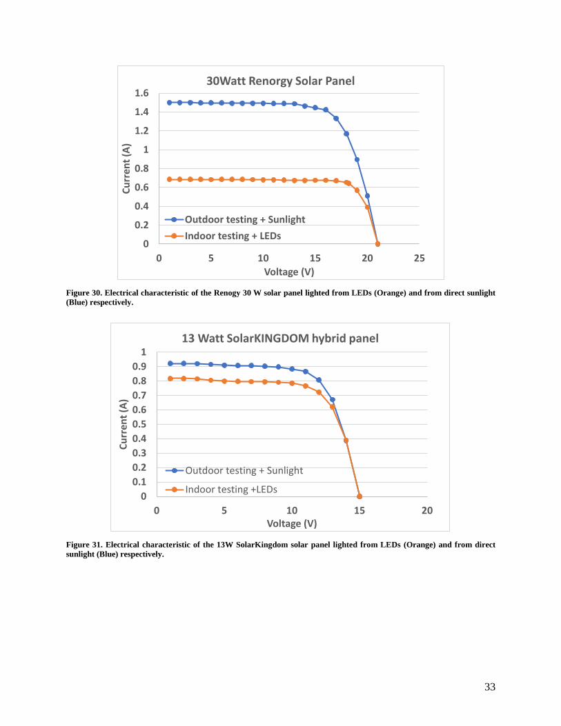
33
Figure 30. Electrical characteristic of the Renogy 30 W solar panel lighted from LEDs (Orange) and from direct sunlight (Blue) respectively.
Figure 31. Electrical characteristic of the 13W SolarKingdom solar panel lighted from LEDs (Orange) and from direct sunlight (Blue) respectively.
0
0.2
0.4
0.6
0.8
1
1.2
1.4
1.6
0 5 10 15 20 25
Curr
ent (
A)
Voltage (V)
30Watt Renorgy Solar Panel
Outdoor testing + SunlightIndoor testing + LEDs
00.10.20.30.40.50.60.70.80.9
1
0 5 10 15 20
Curr
ent (
A)
Voltage (V)
13 Watt SolarKINGDOM hybrid panel
Outdoor testing + Sunlight
Indoor testing +LEDs
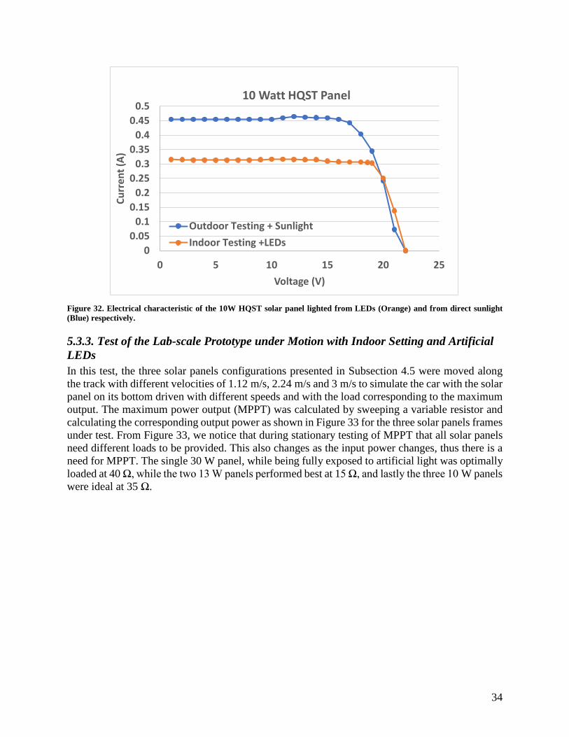
34
Figure 32. Electrical characteristic of the 10W HQST solar panel lighted from LEDs (Orange) and from direct sunlight (Blue) respectively.
5.3.3. Test of the Lab-scale Prototype under Motion with Indoor Setting and Artificial LEDs In this test, the three solar panels configurations presented in Subsection 4.5 were moved along the track with different velocities of 1.12 m/s, 2.24 m/s and 3 m/s to simulate the car with the solar panel on its bottom driven with different speeds and with the load corresponding to the maximum output. The maximum power output (MPPT) was calculated by sweeping a variable resistor and calculating the corresponding output power as shown in Figure 33 for the three solar panels frames under test. From Figure 33, we notice that during stationary testing of MPPT that all solar panels need different loads to be provided. This also changes as the input power changes, thus there is a need for MPPT. The single 30 W panel, while being fully exposed to artificial light was optimally loaded at 40 Ω, while the two 13 W panels performed best at 15 Ω, and lastly the three 10 W panels were ideal at 35 Ω.
00.05
0.10.15
0.20.25
0.30.35
0.40.45
0.5
0 5 10 15 20 25
Curr
ent (
A)
Voltage (V)
10 Watt HQST Panel
Outdoor Testing + SunlightIndoor Testing +LEDs
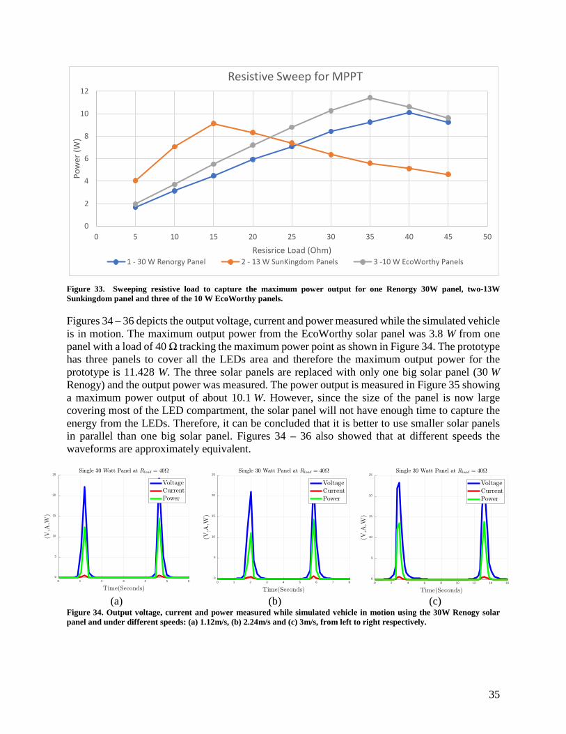
35
Figure 33. Sweeping resistive load to capture the maximum power output for one Renorgy 30W panel, two-13W Sunkingdom panel and three of the 10 W EcoWorthy panels.
Figures 34 – 36 depicts the output voltage, current and power measured while the simulated vehicle is in motion. The maximum output power from the EcoWorthy solar panel was 3.8 W from one panel with a load of 40 Ω tracking the maximum power point as shown in Figure 34. The prototype has three panels to cover all the LEDs area and therefore the maximum output power for the prototype is 11.428 W. The three solar panels are replaced with only one big solar panel (30 W Renogy) and the output power was measured. The power output is measured in Figure 35 showing a maximum power output of about 10.1 W. However, since the size of the panel is now large covering most of the LED compartment, the solar panel will not have enough time to capture the energy from the LEDs. Therefore, it can be concluded that it is better to use smaller solar panels in parallel than one big solar panel. Figures 34 – 36 also showed that at different speeds the waveforms are approximately equivalent.
(a) (b) (c)
Figure 34. Output voltage, current and power measured while simulated vehicle in motion using the 30W Renogy solar panel and under different speeds: (a) 1.12m/s, (b) 2.24m/s and (c) 3m/s, from left to right respectively.
0
2
4
6
8
10
12
0 5 10 15 20 25 30 35 40 45 50
Pow
er (W
)
Resisrice Load (Ohm)
Resistive Sweep for MPPT
1 - 30 W Renorgy Panel 2 - 13 W SunKingdom Panels 3 -10 W EcoWorthy Panels
0 1 2 3 4 5 60
5
10
15
20
25
0 1 2 3 4 5 6 7 80
5
10
15
20
25
0 2 4 6 8 10 12 14 160
5
10
15
20
25
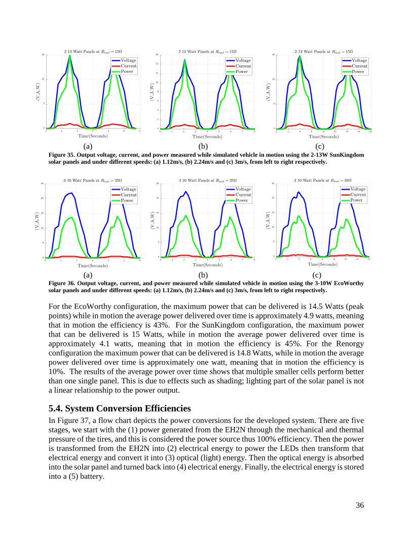
36
(a) (b) (c)
Figure 35. Output voltage, current, and power measured while simulated vehicle in motion using the 2-13W SunKingdom solar panels and under different speeds: (a) 1.12m/s, (b) 2.24m/s and (c) 3m/s, from left to right respectively.
(a) (b) (c) Figure 36. Output voltage, current, and power measured while simulated vehicle in motion using the 3-10W EcoWorthy solar panels and under different speeds: (a) 1.12m/s, (b) 2.24m/s and (c) 3m/s, from left to right respectively.
For the EcoWorthy configuration, the maximum power that can be delivered is 14.5 Watts (peak points) while in motion the average power delivered over time is approximately 4.9 watts, meaning that in motion the efficiency is 43%. For the SunKingdom configuration, the maximum power that can be delivered is 15 Watts, while in motion the average power delivered over time is approximately 4.1 watts, meaning that in motion the efficiency is 45%. For the Renorgy configuration the maximum power that can be delivered is 14.8 Watts, while in motion the average power delivered over time is approximately one watt, meaning that in motion the efficiency is 10%. The results of the average power over time shows that multiple smaller cells perform better than one single panel. This is due to effects such as shading; lighting part of the solar panel is not a linear relationship to the power output.
5.4. System Conversion Efficiencies In Figure 37, a flow chart depicts the power conversions for the developed system. There are five stages, we start with the (1) power generated from the EH2N through the mechanical and thermal pressure of the tires, and this is considered the power source thus 100% efficiency. Then the power is transformed from the EH2N into (2) electrical energy to power the LEDs then transform that electrical energy and convert it into (3) optical (light) energy. Then the optical energy is absorbed into the solar panel and turned back into (4) electrical energy. Finally, the electrical energy is stored into a (5) battery.
0 1 2 3 4 5 60
5
10
15
0 1 2 3 4 5 6 7 80
2
4
6
8
10
12
14
16
0 2 4 6 8 10 12 14 160
5
10
15
0 1 2 3 4 5 60
5
10
15
20
25
0 1 2 3 4 5 6 7 80
5
10
15
20
25
0 2 4 6 8 10 12 14 160
5
10
15
20
25
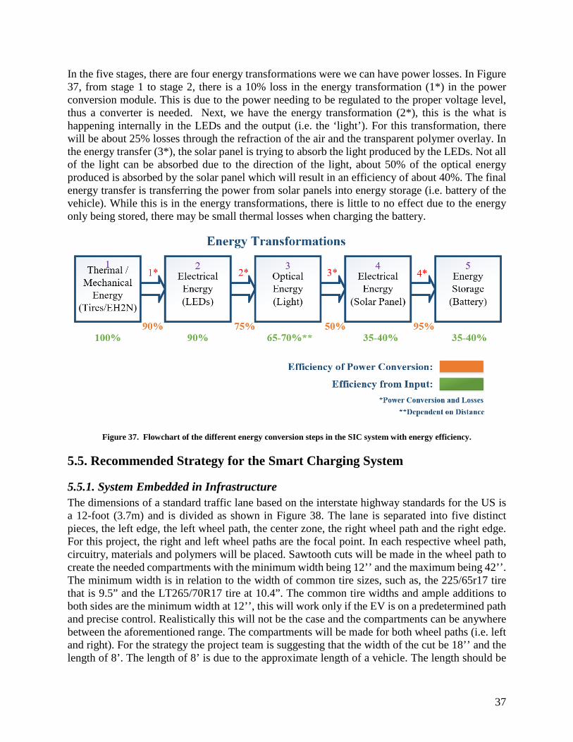
37
In the five stages, there are four energy transformations were we can have power losses. In Figure 37, from stage 1 to stage 2, there is a 10% loss in the energy transformation (1*) in the power conversion module. This is due to the power needing to be regulated to the proper voltage level, thus a converter is needed. Next, we have the energy transformation (2*), this is the what is happening internally in the LEDs and the output (i.e. the ‘light’). For this transformation, there will be about 25% losses through the refraction of the air and the transparent polymer overlay. In the energy transfer (3*), the solar panel is trying to absorb the light produced by the LEDs. Not all of the light can be absorbed due to the direction of the light, about 50% of the optical energy produced is absorbed by the solar panel which will result in an efficiency of about 40%. The final energy transfer is transferring the power from solar panels into energy storage (i.e. battery of the vehicle). While this is in the energy transformations, there is little to no effect due to the energy only being stored, there may be small thermal losses when charging the battery.
Figure 37. Flowchart of the different energy conversion steps in the SIC system with energy efficiency.
5.5. Recommended Strategy for the Smart Charging System
5.5.1. System Embedded in Infrastructure The dimensions of a standard traffic lane based on the interstate highway standards for the US is a 12-foot (3.7m) and is divided as shown in Figure 38. The lane is separated into five distinct pieces, the left edge, the left wheel path, the center zone, the right wheel path and the right edge. For this project, the right and left wheel paths are the focal point. In each respective wheel path, circuitry, materials and polymers will be placed. Sawtooth cuts will be made in the wheel path to create the needed compartments with the minimum width being 12’’ and the maximum being 42’’. The minimum width is in relation to the width of common tire sizes, such as, the 225/65r17 tire that is 9.5” and the LT265/70R17 tire at 10.4”. The common tire widths and ample additions to both sides are the minimum width at 12’’, this will work only if the EV is on a predetermined path and precise control. Realistically this will not be the case and the compartments can be anywhere between the aforementioned range. The compartments will be made for both wheel paths (i.e. left and right). For the strategy the project team is suggesting that the width of the cut be 18’’ and the length of 8’. The length of 8’ is due to the approximate length of a vehicle. The length should be
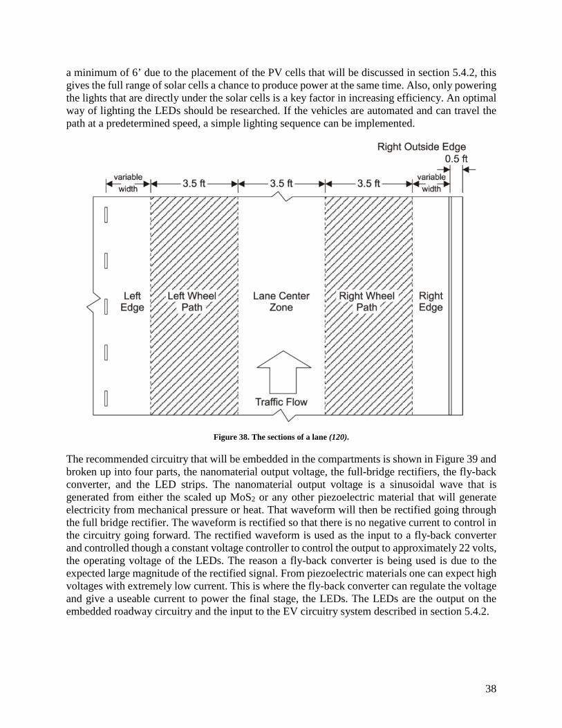
38
a minimum of 6’ due to the placement of the PV cells that will be discussed in section 5.4.2, this gives the full range of solar cells a chance to produce power at the same time. Also, only powering the lights that are directly under the solar cells is a key factor in increasing efficiency. An optimal way of lighting the LEDs should be researched. If the vehicles are automated and can travel the path at a predetermined speed, a simple lighting sequence can be implemented.
Figure 38. The sections of a lane (120).
The recommended circuitry that will be embedded in the compartments is shown in Figure 39 and broken up into four parts, the nanomaterial output voltage, the full-bridge rectifiers, the fly-back converter, and the LED strips. The nanomaterial output voltage is a sinusoidal wave that is generated from either the scaled up MoS2 or any other piezoelectric material that will generate electricity from mechanical pressure or heat. That waveform will then be rectified going through the full bridge rectifier. The waveform is rectified so that there is no negative current to control in the circuitry going forward. The rectified waveform is used as the input to a fly-back converter and controlled though a constant voltage controller to control the output to approximately 22 volts, the operating voltage of the LEDs. The reason a fly-back converter is being used is due to the expected large magnitude of the rectified signal. From piezoelectric materials one can expect high voltages with extremely low current. This is where the fly-back converter can regulate the voltage and give a useable current to power the final stage, the LEDs. The LEDs are the output on the embedded roadway circuitry and the input to the EV circuitry system described in section 5.4.2.
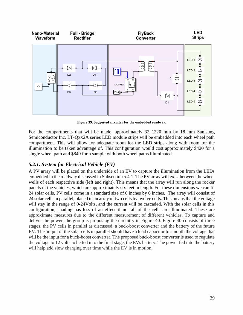
39
Figure 39. Suggested circuitry for the embedded roadway.
For the compartments that will be made, approximately 32 1220 mm by 18 mm Samsung Semiconductor Inc. LT-Qxx2A series LED module strips will be embedded into each wheel path compartment. This will allow for adequate room for the LED strips along with room for the illumination to be taken advantage of. This configuration would cost approximately $420 for a single wheel path and $840 for a sample with both wheel paths illuminated.
5.2.1. System for Electrical Vehicle (EV) A PV array will be placed on the underside of an EV to capture the illumination from the LEDs embedded in the roadway discussed in Subsection 5.4.1. The PV array will exist between the wheel wells of each respective side (left and right). This means that the array will run along the rocker panels of the vehicles, which are approximately six feet in length. For these dimensions we can fit 24 solar cells, PV cells come in a standard size of 6 inches by 6 inches. The array will consist of 24 solar cells in parallel, placed in an array of two cells by twelve cells. This means that the voltage will stay in the range of 0-24Volts, and the current will be cascaded. With the solar cells in this configuration, shading has less of an effect if not all of the cells are illuminated. These are approximate measures due to the different measurement of different vehicles. To capture and deliver the power, the group is proposing the circuitry in Figure 40. Figure 40 consists of three stages, the PV cells in parallel as discussed, a buck-boost converter and the battery of the future EV. The output of the solar cells in parallel should have a load capacitor to smooth the voltage that will be the input for a buck-boost converter. The proposed buck-boost converter is used to regulate the voltage to 12 volts to be fed into the final stage, the EVs battery. The power fed into the battery will help add slow charging over time while the EV is in motion.
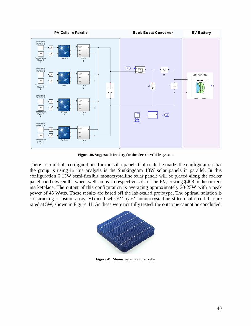
40
Figure 40. Suggested circuitry for the electric vehicle system.
There are multiple configurations for the solar panels that could be made, the configuration that the group is using in this analysis is the Sunkingdom 13W solar panels in parallel. In this configuration 6 13W semi-flexible monocrystalline solar panels will be placed along the rocker panel and between the wheel wells on each respective side of the EV, costing $408 in the current marketplace. The output of this configuration is averaging approximately 20-25W with a peak power of 45 Watts. These results are based off the lab-scaled prototype. The optimal solution is constructing a custom array. Vikocell sells 6’’ by 6’’ monocrystalline silicon solar cell that are rated at 5W, shown in Figure 41. As these were not fully tested, the outcome cannot be concluded.
Figure 41. Monocrystalline solar cells.
41
6. CONCLUSIONS The report presented an innovative smart charging system for future electric vehicles. It is a novel (because it is induction coil-free) wireless charging mechanism that uses nanomaterials-powered LEDs embedded within the road pavement and thin film solar panels placed on the bottom of the electric vehicles to charge the vehicle battery. Light mediates energy transfer between LEDs and solar panels. To better protect the LEDs from the heavy vehicle load whilst still harnessing their electric-to-optical energy conversion capability, certain flexible polymer overlay materials were developed to be placed onto the pavement surface. The report presented the initial, albeit promising, results on the great potential of the nanomaterials to harvest energy and provide electricity to light up the LEDs. However, it was seen that it is challenging to fabricate EH2N in a large scale to be used in practice. The team is currently looking at some other piezoelectric materials that are commercially available and operate based on the similar concept during the implementation phase while still working on enhancing the output of the nanomaterials currently being used. A GFRP was fabricated as an overlay for the nanomaterials for the roadway compartments, the GFRP was tested for mechanical stress to ensure the performance of load testing of the vehicle as well as for electrical conductivity.
A lab-scale proof-of-concept prototype was also demonstrated to verify the system-level capability. Different solar panels were tested, and it was concluded that the solar panel size should be smaller than the LED compartments embedded in the roadways for best results. In addition, it was shown that the best results came from the solar panel that combines the first- and second-generation panel characteristics, thus simultaneously achieving mono-crystalline and flexible. It was shown that the start to end energy efficiency was about 40%. A strategy for actual implementation was proposed for both the embedded roadway and the circuits for the EV. Dimensions of the compartments and the contents of the compartments are discussed as well as the configuration of the solar panels and power stage to charge the battery.
This clean, wireless charging method for electric vehicles, if adapted, means a significant decrease in CO2 emissions. Comparing with a gasoline powered vehicle, the CO2 emission is decreased in EVs from 57 to 28 metric tons of emission, which means a 50% reduction. This will help decrease the climate change, which will otherwise cause damage in the transportation infrastructure through higher temperatures, more severe storms and flooding, and higher storm surges, affecting the reliability and capacity of transportation systems. In addition, with the energy harvested from the pavement using these nanomaterials, the system can also be used as a sensor for vehicle counts and traffic data collection. This sensing technology can help reduce crashes, increase safety as well as improve congestion.
42
REFERENCES 1. Gerssen-Gondelach, S., and Faaij, A. (2012) Performance of batteries for electric vehicles on
short and longer term, Journal of Power Sources, pp. 111.
2. Etacheri, V., Marom, R., Elazari, Salitra, R. and Aurbach, D. (2011) Challenges in the development of advanced Li-ion batteries: A review, Energy Environmental Science 4, pp. 3243.
3. S. Li et. al. (2015) Wireless Power Transfer for Electric Vehicle Applications, IEEE Journal of Emerging and Selected Topics in Power Electronics, pp. 4.
4. Will electric cars soon have solar roofs? Toyota and Tesla say yes, ThinkProgress.org, https://thinkprogress.org/prius-solar-roof-breakthrough-2b929f467061. (2017).
5. Kurs, A., Moffatt, R., Joannopoulos, J., Fisher, P. and M. Soljacic (2007) Wireless power transfer via strongly coupled magnetic resonances, Science, pp. 83–86.
6. Sample, A., Meyer, D. and Smith, J. (2011) Analysis, experimental results, and range adaptation of magnetically coupled resonators for wireless power transfer, IEEE Trans. Ind. Electron., pp. 544–554.
7. Cannon, B., Hoburg, J., Stancil, D. and Goldstein, S. (2009) Magnetic resonant coupling as a potential means for wireless power transfer to multiple small receivers, IEEE Transactions on Power Electronics, pp. 1819–1825.
8. Kurs, A., Moffatt, R., and Soljacic, M. (2010) Simultaneous mid-range power transfer to multiple devices, Applied Physics Letters, pp. 044102-1–044102-3.
9. Sanghoon, C., Yong-Hae, K., Kang, S.-Y., Myung-Lae, L., Jong-Moo, L. and Zyung, T. (2011) Circuit-model-based analysis of a wireless energy transfer system via coupled magnetic resonances, IEEE Trans. Ind. Electron., pp. 2906–2914.
10. Kainan, C., and Zhengming, Z. (2013) Analysis of the double-layer printed spiral coil for wireless power transfer, IEEE J. Emerg. Sel. Topics Power Electron., pp. 114–121.
11. Yiming, Z., Zhengming, Z. and Kainan, C. (2014) Frequency decrease analysis of resonant wireless power transfer, IEEE Trans. Power Electron., pp. 1058–1063.
12. Kavimandan, U. et al, (2019) Analysis of Dead-Time in a Single Phase Wireless Power Transfer System, 2019 IEEE Transportation Electrification Conference and Expo (ITEC), Detroit, MI, USA, pp. 1-8.
13. Bai, T. et al, (2019) Machine Learning-Assisted Wireless Power Transfer based on Magnetic Resonance, in IEEE Access.
14. Chu, S. and Avestruz, A. (2019) A New Calibration Strategy for Transfer-Power Measurement of Wireless Charging of Electric Vehicles, 2019 IEEE Transportation Electrification Conference and Expo (ITEC), Detroit, MI, USA, pp. 1-5.
15. Mohammad, M. et al., (2019) Sensitivity Analysis of an LCC-LCC Compensated 20-kW Bidirectional Wireless Charging System for Medium-Duty Vehicles, 2019 IEEE Transportation Electrification Conference and Expo (ITEC), Detroit, MI, USA, 2019, pp. 1-7.
43
16. Ayachit, A., Abdul-Hak, M. and Kazimierczuk, M. (2019) Transfer Functions of Wireless Power Transfer Systems with Series and Series-Parallel Compensation Schemes, 2019 IEEE Transportation Electrification Conference and Expo (ITEC), Detroit, MI, USA, 2019, pp. 1-6.
17. Nagatsuka, Y., Ehara, N., Kaneko, Y., Abe, S., and Yasuda, T. (2010) Compact contactless power transfer system for electric vehicles, in Proc. IPEC, pp. 807–813.
18. Sungwoo, L., Jin, H., Changbyung, P., Nam-Sup, C., Gyu-Hyeoung, C., and Chun-Taek, R. (2010) On-line electric vehicle using inductive power transfer system, in Proc. IEEE ECCE, pp. 1598–1601.
19. Jin, H., Wooyoung, L., Gyu-Hyeong, C., Byunghun, L., and Chun-Taek, R. (2011) Characterization of novel inductive power transfer systems for on-line electric vehicles, in Proc. 26th Annu. IEEE APEC Expo., pp. 1975–1979.
20. Puqi, N., Miller, J. M., Onar, O., and White, C. (2013) A compact wireless charging system development, in Proc. IEEE ECCE, pp. 3629–3634.
21. Nguyen, T.-D., Li, S., Li, W. and Mi, C. (2014) Feasibility study on bipolar pads for efficient wireless power chargers, in Proc. APEC Expo.
22. Caughill, P. (2017) This high-tech, solar-powered car may be the future of travel, https://futurism.com/this-futuristic-solar-powered-car-may-be-the-future-of-travel/.
23. Vandevoorde, G. and Puers, R. (2001) Wireless energy transfer for stand-alone systems: a comparison between low and high power applicability, Sensors and Actuators A:Physical, vol. 92, pp. 305-311.
24. Garnica, J., Casanova, J. and Lin, J. (2011) High efficiency midrange wireless power transfer system, IEEE MTT-S Int. Microw. Syst. Dig., pp. 73–76.
25. Kurs, A. et al, (2007) Wireless power transfer via strongly coupled magnetic resonances, Sciencexpress, vol. 317, pp. 83–86.
26. Waffenschmidt, E. and Staring, T. (2009) Limitation of inductive power transfer for consumer applications, IEEE European Conference on Power Electronics and Applications, pp. 1-10.
27. Suh, Y.-H. and Chang, K. (2002) A high-efficiency dual frequency rectenna for 2.45- and 5.8-GHz wireless power transmission, IEEE Transactions on Microwave Theory and Techniques, vol. 50, no. 7.
28. Raavi, S. et al., (2013) An optical wireless power transfer system for rapid charging, 2013 Texas Symposium on Wireless and Microwave Circuits and Systems (WMCS), Waco, TX.
29. Peng, C. (2007) Method and apparatus for optical wireless charging, US2007/0114967 A1.
30. Lu, X., Niyato, D., Wang, P., Kim, D. and Han, Z. (2015) Wireless charger networking for mobile devices: Fundamentals, standards, and applications, IEEE Wireless Communications, vol. 22, no. 2, pp. 126–135.
31. Costanzo, A., Dionigi, M., Masotti, D., Mongiardo, M., Monti, G., Tarricone, L. and Sorrentino, R. (2014) Electromagnetic energy harvesting and wireless power transmission: A unified approach, Proceedings of the IEEE, vol. 102, no. 11, pp. 1692–1711.
44
32. Lee, J. (2018) Permanent, Wireless self-charging system using NIR band, https://phys.org/news/2018-10-permanent-wireless-self-charging-nir-band.html
33. Zhang, Q., et al, (2018) Distributed Laser Charging: A Wireless Power Transfer Approach, in IEEE Internet of Things Journal, vol. 5, no. 5, pp. 3853-3864.
34. Iyer, V. et al, (2018) Charging a Smartphone Across a Room Using Lasers. Proc. ACM Interact. Mob. Wearable Ubiquitous Technol. 1, 4, Article 143, 21 pages. DOI: https://doi.org/10.1145/3161163
35. Lufčić, M., Maras, M. and Vukelić, M. (2011) Energy saving design and materials in road transport, REACT Conference, http://bib.irb.hr/prikazi-rad?rad=540022.
36. Lee, K. (2013) Students Install the World’s First Solar Pavement Panels in Virginia, Inhabitat, https://inhabitat.com/students-install-the-worlds-first-solar-pavement-panels-in-virginia/.
37. SolaRoad, http://www.solaroad.nl., Accessed March 24, 2019.
38. Liggett, B. (2011) The Netherlands to Pave Roads with Solaroad Solar Panels, Inhabitat, https://inhabitat.com/the-netherlands-to-pave-roads-with-solaroad-solar-panels/.
39. Dutch Company Drives New Solar Power, http://www.ecmag.com/section/miscellaneous/dutch-company-drives-new-solar-power, Accessed March 24, 2019.
40. Scott, C. (2014) Following the Solar Brick Road to Clean Energy and Smart Roadways, SingularityHub, https://singularityhub.com/2014/05/22/following-the-solar-brick-road-to-clean-energy-and-smart-roadways/.
41. Reich, J. (2015) The Daejeon-Sejong Bike Highway Is Solar Powered And Good For The Environment, Tech Times, http://www.techtimes.com/articles/72306/20150727/daejeon-sejong-bike-highway-solar-powered-good-environment.htm.
42. Tsagas, I. (2016) France gets a step closer to solar roads, PV Magazine, https://www.pv-magazine.com/2016/08/04/france-gets-a-step-closer-to-solar-roads_100025671/.
43. Bourgin, Y. (2016) High Tech. Ségolène Royal lance la première route solaire dans l'Orne, Entreprises, https://www.ouest-france.fr/environnement/amenagement-du-territoire/high-tech-segolene-royal-lance-la-premiere-route-solaire-dans-l-orne-4582630.
44. Kim, W. (2016) World's first solar panel road opens in Normandy village, theguardian.
45. Ranjan, R., (2015) Solar Power Roads: Revitalising Solar Highways, Electrical Power and Smart Grids, International Journal of Engineering Research and General Science, pp. 380–385.
46. Bobes-Jesus, V., Pascual-Munoz, P., Castro-Fresno, D., and Rodriguez-Hernandez, J. (2013) Asphalt solar collectors: a literature review, Applied Energy 102, pp. 962-70.
47. Lowe, J. (1979) Paving and solar energy system and method, Inventor: Wendel, I.L. United States, patent of invention US 4.132.074, 01-02-1979.
48. Larsson, O., Thelandersson, S. (2011) Estimating extreme values of thermal gradients in concrete structures, Mater. Struct., pp. 1491-1500.

45
49. Gao, Q., Huang, Y., Li, M., Liu, Y., and Yan, Y.Y. (2010) Experimental study of slab solar collection on the hydronic system of road, Solar Energy, pp. 2096-2102.
50. Zhao, J., Wang, H., Chen, Z., and Qu, H. (2006) Seasonal behavior of pavement in geothermal snow-melting system with solar energy storage, Trans Tianjin University, pp. 319-324.
51. Liu, X., Rees, S.J., and Spitler, J. (2007) Modeling snow melting on heated pavement surfaces. Part I: Model development, Applied Thermal Engineering, pp. 1115-1124.
52. Tu, Y., Li, J., and Guan, C. (2010) Heat transfer analysis of asphalt concrete pavement based on snow melting, International Conference on Electrical and Control Engineering (ICECE), pp. 3795–8.
53. Wu, S., Chen, M. and Zhang, J. (2011) Laboratory investigation into thermal response of asphalt pavements as solar collector by application of small-scale slabs, Applied Thermal Engineering, pp. 1582-1587.
54. Navarro, G., Rojas, C. (2017) Piezoelectric power generating tire apparatus, US20170084817A1.
55. Kumar, A., and Sumathi, S. (2015) Renewable energy source piezo electric harvesters in car tyres, 2015 Online International Conference on Green Engineering and Technologies.
56. Makki, N. et. al. (2011) Piezoelectric power generation for sensor applications: design of a battery-less wireless tire pressure sensor, pp. 806618, SPIE.
57. Hollaway, L. (2003) The evolution of and the way forward for advanced polymer composites in the civil infrastructure, Construction and Building Materials, pp. 365–378.
58. Einde, L., Zhao, L. and Seible, F. (2013) Use of FRP composites in civil structural applications, Construction and Building Materials, pp. 389–403.
59. Guide for the Design and Construction of Externally Bonded FRP Systems for Strengthening Concrete Structures (2008) American Concrete Institute.
60. Bank, L. (2006) Composites for construction: structural design with FRP materials, USA: John Wiley & Sons.
61. Genedy, M., Chennareddy, R., Soliman, E., Kandil, U. F., Taha, M. (2017) Improving Shear Strength of GFRP Bolted Lap Joints Using Carbon Nanotubes, Journal of Reinforced Plastics and Composites, pp. 958-971.
62. Genedy, M., Daghash, S., Soliman, E. and Taha, M. (2015) Improving Fatigue Performance of GFRP Composites Using Carbon Nanotubes, Fibers, pp. 3-29.
63. Al-Sabagh, A., Taha, M., Kandil, U., Awadallah, A., Nasr, G., and Taha, M. (2017) Monitoring moisture damage propagation in GFRP composites using carbon nanoparticles, Polymer.
64. Federal Highway Administration (FHWA) (2017) High Friction Surface Treatment, fact sheet, FHWA, https://safety.fhwa.dot.gov/roadway_dept/pavement_friction/high_friction/.
46
65. Emiroglu, M., Douba, A., Tarefder, R., Kandil, U., and Taha, M. (2017) New Polymer Concrete with Superior Ductility and Fracture Toughness Using Alumina Nanoparticle, ASCE Journal of Materials in Civil Engineering.
66. Szarka, G., Stark, B. and Burrow, S. (2012) Review of Power Conditioning for Kinetic Energy Harvesting Systems, in IEEE Transactions on Power Electronics, pp. 803-815.
67. Burrow, S. and Clare, L. (2009) Open-loop power conditioning for vibration energy harvesting, Electronics Letters, pp. 999–1000.
68. Arnold, D. (2007) Review of microscale magnetic power generation, IEEE Transactions Magazine, pp. 3940–3951.
69. Mitcheson, P., Yeatman, E., Rao, G., Holmes, A. and Green, T. (2008) Energy harvesting from human and machine motion for wireless electronic devices, Proc. IEEE, pp. 1457–1486.
70. Lefeuvre, E., Badel, A., Benayad, A., Lebrun, L., Richard, C., and Guyomar D. (2005) A comparison between several approaches of piezoelectric energy harvesting, J. Phys. IV France, pp. 177–186.
71. Liu, W., Feng, Z., He, J., and Liu, R. (2007) Maximum mechanical energy harvesting strategy for a piezoelement, Smart Mater. Struct., pp. 2130–2136.
72. Hande, A., Rajasekaran, A., and Bhatia, D. (2008) Buck-boost converter based power conditioning circuit for low excitation vibration energy harvesting, presented at the 3rd Annu. Austin Conf. Integrated Circuits and Systems, Austin, TX, [Online]. http://www.texasmicropower.com/publications/ArvindhR UTD EH FullPaper.pdf
73. Clare, L. and Burrow, S. (2008) Power conditioning for energy harvesting, in Proc. SPIE Active Passive Smart Struct. Integr. Syst, San Diego, CA, pp. 69280A-1–69280A-13.
74. Peters, C., Kessling, O., Henrici, F., Ortmanns, M., and Manoli, Y. (2007) CMOS integrated highly efficient full wave rectifier, in Proc. IEEE Int. Symp. Circuits Syst., New Orleans, LA, pp. 2415–2418.
75. Seeman, M., Sanders, S., and Rabaey, J. (2008) An ultra-low-power power management IC for energy-scavenged Wireless Sensor Nodes, in Proc. IEEE Power Electron. Spec. Conf., Rhodes, Greece, pp. 925– 931.
76. Le, T., Han, J., Jouanne, A., Mayaram, K., and Fiez T. (2006) Piezoelectric micro-power generation interface circuits, IEEE J. Solid-State Circuits, vol. 41, no. 6, pp. 1411–1420.
77. Xu, S., Ngo, K., Nishida, T., Chung, G., and Sharma, A. (2007) Low frequency pulsed resonant converter for energy harvesting, IEEE Trans. Power Electron., pp. 63–68.
78. Marinkovica, D., Freyb, A., Kuehneb, I., and Scholla, G. (2009) A new rectifier and trigger circuit for a piezoelectric microgenerator, in Proc. Euro sensors XXIII Conf., Lausanne, Switzerland, pp. 1447–1450.
79. Lin, P. (1977) Topological generation and analysis of voltage multiplier circuits, IEEE Trans. Circuits Syst., pp. 517–530.
47
80. Tse, C., Wong, S., and Chow, M. (1995) On lossless switched capacitor power converters, IEEE Trans. Power Electron, pp. 286–291.
81. Seeman, M. and Sanders, S. (2006) Analysis and optimization of switched capacitor DC-DC converters, in Proc. IEEE COMPEL Workshop, Troy, NY, pp. 216–224.
82. Favrat, P., Deval, P., and Declercq, M. (1998) A high-efficiency CMOS voltage doubler, IEEE J. Solid-State Circuits, pp. 410–416.
83. Zhu, Z., Jamali, B., and Cole, P. (2004) Brief comparison of different rectifier structures for HF and UHF RFID (Phase I), Auto-ID Labs, Adelaide,Australia,[Online]. http://autoidlab.eleceng. adelaide.edu.au/Papers/CompRect.pdf
84. Torah, R., Glynne-Jones, P., Tudor, M., O’Donnell, T., Roy, S., and Beeby, S. (2008) Self-powered autonomous wireless sensor node using vibration energy harvesting, Meas. Sci. Technol., pp. 1–8.
85. Lehmann, T. and Moghe, Y. (2005) On-chip active power rectifiers for biomedical applications, in Proc. IEEE Int. Symp. Circuits Syst., Kobe, Japan, pp. 732–735.
86. Seemanand, M.D., Sanders, S. (2006) Analysis and optimization of switched capacitor DC-DC converters, in Proc. IEEE COMPEL Workshop, Troy, NY, pp. 216–224.
87. Dallago, E., Miatton, D., Venchi, G., Bottarel, V., Frattini, G., Ricotti, G., and Schipani, M. (2008) Active self supplied AC–DC converter for piezoelectric energy scavenging systems with supply independent bias, in Proc. IEEE Int. Symp. Circuits Syst., Seattle, WA, pp. 1448–1451.
88. Cheng, S., Jin, Y., Rao, Y., and Arnold, D. P. (2009) A bridge voltage doubler AC/DC converter for low-voltage energy harvesting applications, in Proc. Power MEMS, Washington, DC, pp. 25–28.
89. Salmon, J. (1993) Circuit topologies for single-phase voltage-doubler boost rectifiers, IEEE Trans. Power Electron., pp. 521–529.
90. Dwari, S. and Parsa, L. (2008) Efficient low voltage direct AC/DC converters for self-powered wireless sensor nodes and mobile electronics, in Proc.30th IEEE Int. Telecommun. Energ Conf., San Diego, CA, pp.1–7.
91. Dwari, S. and Parsa, L. (2010) An efficient AC–DC step-up converter for low voltage energy harvesting, IEEE Trans. Power Electron, pp. 2188–2199.
92. Mitcheson, P., Green, T., and Yeatman, E. (2007) Power processing circuits for electromagnetic, electrostatic and piezo electric inertial energy scavengers, Microsyst. Technol., pp. 1629–1635.
93. Richard, C., Guyomar, D., Audigier, D., and Ching, G. (1999) Semi passive damping using continuous switching of a piezoelectric devices, in Proc. SPIE Int. Symp. Smart Struct. Materials: Damping and Isolation, pp. 104–111.
94. Guyomar, D., Richard, C., Badel, A., Lefeuvre, E., and Lallart, M. (2009) Energy harvesting using non-linear techniques, in Energy Harvesting
48
Tecnologies,D.J.InmanandS.Priya,Eds.,1sted. NewYork: Springer Science Business Media LLC, pp. 209–266.
95. Guyomar, D., Badel, A., Lefeuvre, E., and Richard, C. (2005) Toward energy harvesting using active materials and conversion improvement by nonlinear processing, IEEE Trans. Ultrason., Ferroelectr., Freq. Control, pp. 584–595.
96. Shu, Y., Lien, I., and Wu, W. (2007) An improved analysis of the SSHI interface in piezo electric energy harvesting, Smart Mater. Struct., pp. 2253–2264.
97. Ramadass, Y. and Chandrakasan, A. (2010) An efficient piezoelectric energy harvesting interface circuit using a bias-flip rectifier and shared inductor, IEEE J. Solid-State Circuits, pp. 189–204.
98. Lee, H. and Mok, P. (2007) An SC voltage doubler with pseudo-continuous output regulation using a three-stage switchable opamp, IEEE J. Solid State Circuits, pp. 1216–1229.
99. Lam, Y., Ki, W., and Tsui, C. (2006) An integrated 1.8V to 3.3V regulated voltage doubler using active diodes and dual-loop voltage follower for switch-capacitive load, in Proc. Symp. VLSI Circuits Dig. Tech. Papers, pp. 85–86.
100. Carlson E., Strunz K., and Otis B. (2010) A 20mV input boost converter with efficient digital control for thermoelectric energy harvesting, IEEE J. Solid-State Circuits, pp. 741–750.
101. Lefeuvre, E., Audigier, D., Richard, C., and Guyomar, D. (2007) Buck-boost converter for sensorless power optimization of piezoelectric energy harvester, IEEE Trans. Power Electron., pp. 2018–2025.
102. Peláez, E. A; Villegas, E. R (2007). LED power reduction trade-offs for ambulatory pulse oximetry. 29th Annual International Conference of the IEEE Engineering in Medicine and Biology Society. 2007. pp. 2296–9.
103. Solid-State Lighting: Comparing LEDs to Traditional Light Sources. eere.energy.gov. Archived from the original on May 5, 2009.
104. Lifetime of White LEDs. US Department of Energy. Retrieved on March 16, 2012.
105. In depth: Advantages of LED Lighting. energy.ltgovernors.com
106. Anton, S., Erturk, E., Kong, N., Ha, D., and Inman, D. (2009) Self-charging structures using piezoceramics and thin-film batteries, in Proc. ASME Conf. Smart Mater., Adaptive Struct. Intell. Syst., Oxnard, CA, pp. 1–11.
107. Quaschning, V. (2005) Understanding Renewable Energy Sources.
108. Lund, H., Nilson, R., Solamatova, D. & Skare, E. (2008) The History Highlight of Solar Cells. http://org.ntnu.no/solarcells/pages/history.php Accessed October, 2008
109. Prashant, A. (2018) Literature Review on Photovoltaic Panels, International Journal of Emerging Research in Management & Technology.
110. Manzeli S. et al. (2017). 2D transition metal dichalcogenides. Nature Reviews Materials 2, 17033.
49
111. Radisavljevic B. et al. (2011). A single-layer MoS2 transistors, Nature Nanotechnology. 6, 147.
112. Splendiani A. et al. (2010). Emerging photoluminescence in monolayer MoS2, Nano Letters. 10, 1271.
113. Butler S. et al. (2013). Progress, challenges, and opportunities in two-dimensional materials beyond graphene. ACS Nano 7, 2898.
114. Wu W. et al. (2014). Piezoelectricity of single-atomic-layer MoS2 for energy conversion and piezotronics. Nature. 514, 470.
115. Zhu H. et al. (2015). Observation of piezoelectricity in free-standing monolayer MoS2. Nature Nanotechnology. 10, 151.
116. Buscema, M. et al. (2013) Large and Tunable Photothermoelectric Effect in Single-Layer MoS2, Nano Letters, pp. 358-363
117. Okogbue E. et al. (2018). Centimeter-Scale Periodically Corrugated Few-Layer 2D MoS2 with Tensile Stretch-Driven Tunable Multifunctionalities. ACS Applied Materials and Interfaces. 10, 30623.
118. Ferrari A. et al. (2006). Raman Spectrum of Graphene and Graphene Layers. Phys. Rev. Lett. 97, 187401.
119. Khalili, M. et al. (2019). Electro-mechanical characterization of a piezoelectric energy harvester. Applied Energy. 10.1016/j.apenergy.2019.113585.
120. Diefenderfer, Brian & James W. Bryant, Jr. (2006). Development of a Pavement Warranty Contract and Performance Specification for a Hot-Mix Asphalt Resurfacing Project. Proceedings of the 2006 Airfield and Highway Pavement Specialty Conference. 2006. 10.1061/40838(191)84.