Embed Size (px)
Citation preview

Application Report SCAA073 – August 2004
1
Small Package, Big Performance Heather McClendon / Kal Mustafa High Performance Analog
ABSTRACT
This application report presents phase jitter and phase noise measurements of four differential clock drivers. Two Texas Instruments devices were compared to two independent competitor devices. This report proves that clock buffer selection does have an impact on the total system timing budget. In addition, the report explains the types of jitter and their causes.
The CDCM1804 and CDCM1802 are ideal for a variety of applications in both telecom and datacom. Existing designs include but are not limited to: backplanes, medical imaging, and basestations. The CDCM1804 and CDCM1802 are also good solutions for driving DACs and ADCs including, DAC568x, ADS55xx, and TLK/SLK product lines from Texas Instruments.
Contents 1 Introduction .....................................................................................................................................2
1.1 Definitions..................................................................................................................................2 1.2 Test Setup .................................................................................................................................2
2 Measurement Data ..........................................................................................................................2 2.1 PN9000 Results ........................................................................................................................2
2.1.1 CDCM1804 and Competitor A.......................................................................................2 2.1.2 CDCM1802 and Competitor B.......................................................................................2
3 Summary..........................................................................................................................................2 Appendix A. .............................................................................................................................................2 References...............................................................................................................................................2
SCAA073
2 Small Package, Big Performance
Figures Figure 1. Test Setup for Phase Noise Measurements Taken from the AeroFlex PN9000............2 Figure 2. PN9000 RMS Phase Jitter Measurements of the CDCM1804 and Competitor A ..........2 Figure 3. PN9000 Peak-to-Peak Phase Jitter Measurements of the CDCM1804 and
Competitor A.......................................................................................................................2 Figure 4. PN9000 Unit Interval (UI) Phase Jitter Measurements of the CDCM1804 and
Competitor A.......................................................................................................................2 Figure 5. PN9000 RMS Phase Jitter Measurements of the CDCM1802 and Competitor B ..........2 Figure 6. PN9000 Peak-to-Peak Phase Jitter Measurements of the CDCM1802 and
Competitor B.......................................................................................................................2 Figure 7. PN9000 Unit Interval Phase Jitter Measurements of the CDCM1802 and
Competitor B.......................................................................................................................2 Figure 8. Phase Noise Plots of the CDCM1804 and Competitor A at 50 MHz, 3.3 V ....................2 Figure 9. Phase Noise Plots of the CDCM1804 and Competitor A at 106.25 MHz, 3.3 V .............2 Figure 10. Phase Noise Plots of the CDCM1804 and Competitor A at 156.25 MHz, 3.3 V .............2 Figure 11. Phase Noise Plots of the CDCM1804 and Competitor A at 622.08 MHz, 3.3 V .............2 Figure 12. Phase Noise Plots of the CDCM1804 and Competitor A at 50 MHz, 2.5 V ....................2 Figure 13. Phase Noise Plots of the CDCM1804 and Competitor A at 106.25 MHz, 2.5 V .............2 Figure 14. Phase Noise Plots of the CDCM1804 and Competitor A at 156.25 MHz, 2.5 V .............2 Figure 15. Phase Noise Plots of the CDCM1804 and Competitor A at 622.08 MHz, 2.5 V .............2 Figure 16. Phase Noise Plots of the CDCM1802 and Competitor B at 50 MHz, 3.3 V ....................2 Figure 17. Phase Noise Plots of the CDCM1802 and Competitor B at 106.25 MHz, 3.3 V .............2 Figure 18. Phase Noise Plots of the CDCM1802 and Competitor B at 156.25 MHz, 3.3 V .............2 Figure 19. Phase Noise Plots of the CDCM1802 and Competitor B at 622.08 MHz, 3.3 V .............2 Figure 20. Phase Noise Plots of the CDCM1802 and Competitor B at 50 MHz, 2.5 V ....................2 Figure 21. Phase Noise Plots of the CDCM1802 and Competitor B at 106.25 MHz, 2.5 V .............2 Figure 22. Phase Noise Plots of the CDCM1802 and Competitor B at 156.25 MHz, 2.5 V .............2 Figure 23. Phase Noise Plots of the CDCM1802 and Competitor B at 622.08 MHz, 2.5 V .............2

SCAA073
Small Package, Big Performance 3
1 Introduction This application report presents data proving that clock buffer selection is important when designing a system with critical timing budget requirements. The test results in this report were obtained under almost ideal conditions (clean power supply, no other noise source (such as close-by ICs) near the device under test (DUT), room temperature). Note that in an actual system, jitter results would likely be higher and therefore using devices with the highest noise margin is the best choice.
Among the many applications, synchronous optical network (SONET) has one of the most stringent jitter and skew requirements and system-timing budgets are normally tight. SONET is synchronous by definition and therefore has strict jitter requirements; 4-ps and1-ps RMS jitter are the maximum allowed over the 12 kHz – 20 MHz bandwidth for OC-48 and OC-192 systems, respectively.
1.1 Definitions
The timing budget is defined by dynamic (jitter) and static errors (skew). Depending on the system architecture, a sub-set of parameters out of the datasheet is only affecting the timing budget. Jitter is a timing distribution of the clock signal and expresses the edge deviation from ideal. Jitter is composed of both deterministic and random (Gaussian) content.
Jitter is any edge deviation from the ideal. The causes of jitter include: power supply noise, thermal and mechanical noise from the input signal, reflection, EMI, and random noise. A few suggestions for reducing jitter include: power supply bypassing (10 µF - 47 µF) to prevent voltage droop and ripple due to current surges, filtering each VCC pin (w/ 0.1 µF) low effective series resistance capacitor, using proper termination, using differential signaling as opposed to single-ended signaling, and minimizing noise coupling by isolating other high frequency signals from the clock driver.
Period jitter is the deviation in cycle time of a signal with respect to an ideal period over a random sample of cycles. Period jitter is important since it includes the max/min frequency and it specifics the shortest clock period. It is important for the set-up and hold-time budget. Calculation with period jitter is sufficient for sub-systems using clock and data signals derived by the same clock source. Use phase jitter to calculate your jitter budget in case a signal comes into such subsystem from an external clock source (e.g. use of ADC, SerDes) or is generated from the clock source that feeds the clock buffer of interest. Period jitter can be measured with any oscilloscope. The trigger input and signal input both must be driven from the output of the clock driver.
Peak-to-peak period jitter is the total jitter range from minimum to maximum values of a clock signal. Peak-to-peak jitter increases indefinite with recording time. Thus, peak-to-peak jitter values are only meaningful if either the recording length or the relative bit error rate is known.
RMS period jitter is one standard deviation (1σ) of the PP jitter of a clock signal. RMS jitter is only valid for Gaussian (normal) distribution. RMS jitter is independent of the sampling window, and thus, better suited to compare performance of two or more devices where sampling time window differs or is unknown.

SCAA073
4 Small Package, Big Performance
Cycle-to-cycle (CC) period jitter, aka adjacent cycle jitter, is the variation in cycle time of a signal between consecutive cycles, over a random sample of successive cycle pairs. CC jitter is also a good value to calculate the setup and hold-time budget since it defines the min/max variation of the timing variation from ideal for the next clock edge.
Phase jitter or accumulated jitter is the absolute deviation of a clock edge from its ideal position in timing. While period jitter only accounts the variation between clock periods, phase jitter accumulates the error of each period and therefore is always bigger. The wider the recording time window is, the more frequency bandwidth becomes integrated into the total phase jitter. Phase jitter can also be measured by integrating phase noise over the frequency band of interest. Either way, the system designer must specify the minimum and maximum frequency for the integration.
For setup and hold-time budget calculation the peak-to-peak value of the phase jitter is important. Note that only the added phase noise by the clock driver is of interest to find the worse edge position between the master clock in the system and the subsystem. The absolute phase jitter of the master clock itself adds to all clock signals in the system, thus canceling its effect.
Analog-to-digital converter (ADC) and SerDes System:
When using AD converter and SerDes transceiver, the incoming data are often sourced by a completely independent clock source and not synchronized to the main system clock (at least no short-term synchronization). Thus, the absolute phase jitter becomes important. A lower frequency band limit must be established (e.g., 12 kHz to full range). For the AD converter, the limit on the low side relates to the sampling window of the ADC that becomes further processed by digital algorithms (e.g. DSP tap size for a FFT). For a SerDes PLL, low Phase jitter is critical around the PLL’s bandwidth. Thus jitter frequency has an upper and low limit (e.g., 12 kHz - 20 MHz for the OC48).
Phase jitter can be measured with any oscilloscope. The trigger input must be fed by the clock signal driving the clock buffer under test while the scope signal input must be driven from the output of the clock buffer under test.
Phase noise (PN) is the short-term instability caused by variation of frequency (phase) of a signal referenced to the carrier level and a function of the carrier offset (i.e., relative noise level within a 1-Hz bandwidth). Integration of PN over a given frequency band yields phase jitter RMS.
1.2 Test Setup
The CDCM1804 is a 3.3 V, 1:3 LVPECL (low voltage positive emitter coupled logic) clock driver with an additional LVCMOS (low voltage complementary metal-oxide semiconductor) output and programmable divider. The CDCM1802 is a 3.3 V, 1:1 LVPECL clock driver with a programmable divider and single LVCMOS output. Both the CDCM1804 and the CDCM1802 are characterized for industrial temperature (-40°C to 85°C) and have a maximum operating frequency of 800-MHz LVPECL and 200-MHz LVCMOS. All measurements were taken using an LVPECL output from the DUT.
SCAA073
Small Package, Big Performance 5
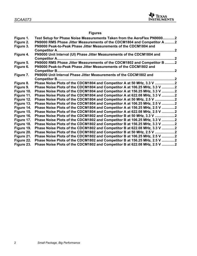
The phase noise measurements, which can be found in Appendix A, were taken by the AeroFlex PN9000 Phase Noise Measurement System using the PLL Synthesizer measurement technique. A Marconi 2041 signal generator was used as the low noise frequency source. The PN9000 was then used to execute the phase jitter measurements for the 12 kHz – 20 MHz frequency bandwidth, the results of which are listed in the following charts. The block diagram of the test setup is shown in Figure 1.
Areoflex PN9000Phase Noise
Measurement System
DUTCDCM1804/CDCM1802/Competitors
A-B
HP6624A SystemDC Power Supply
3.3 V/2.5 V
+
+
--
OUT+
OUT -Marconi 2041 Signal
Generator+
Tektronix TDS694C4-Channel Digital
Real-TimeOscilloscope
IN +
IN -
Figure 1. Test Setup for Phase Noise Measurements Taken from the AeroFlex PN9000

SCAA073
6 Small Package, Big Performance
2 Measurement Data
2.1 PN9000 Results
2.1.1 CDCM1804 and Competitor A
RMS Phase Jitter
0
200
400
600
800
1000
1200
1400
1600
1800
2000
Frequency
Jitte
r in
fs
Signal Generator 719.57 342.52 350.77 88.2
M1804 (3.3V) 1920 450.16 784.72 94.73
Competitor A (3.3V) 1590 666.55 711.47 108.69
M1804 (2.5V) 1300 426.52 441.43 92.12
Competitor A (2.5V) 1070 502.89 529.18 109.82
M1804 (output ÷ 2) (3.3V) 875.78 316.21 363.13 57.27
M1804 (output ÷ 2) (2.5V) 761.21 287.1 306.79 59.73
50MHz 106.25MHz 156.25MHz 622.08MHz
Figure 2. PN9000 RMS Phase Jitter Measurements of the CDCM1804 and Competitor A
2.1.1.1 Testing at 3.3-V Supply
As can be seen from the graph in Figure 2, the CDCM1804 has both lower and higher RMS phase jitter than competitor A depending on the frequency. Yet when the CDCM1804’s output is divided by two, it has RMS phase jitter that is almost half that of competitor A.
2.1.1.2 Testing at 2.5-V Supply
Figure 2 shows similar results where the CDCM1804 has lower RMS phase jitter than competitor A at the three highest frequencies tested and only slightly higher at the lowest frequency tested. However, when the output of the CDCM1804 is divided by two using the programmable divider its RMS phase jitter is consistently lower than that of competitor A.

SCAA073
Small Package, Big Performance 7
PP Phase Jitter
0
1
2
3
4
5
6
7
8
9
10
Frequency
Jitte
r in
fs
Signal Generator 4.26 2.01 2.07 0.52918
M1804 (3.3V) 9.08 2.65 3.79 0.56837
Competitor A (3.3V) 9.46 3.96 4.21 0.65214
M1804 (2.5V) 6.27 2.51 2.6 0.55273
Competitor A (2.5V) 6.3 2.97 3.13 0.65891
M1804 (output ÷ 2) (3.3V) 5.25 1.84 2.08 0.34359
M1804 (output ÷ 2) (2.5V) 3.9 1.67 1.77 0.35837
50MHz 106.25MHz 156.25MHz 622.08MHz
Figure 3. PN9000 Peak-to-Peak Phase Jitter Measurements of the CDCM1804 and Competitor A
The graph in Figure 3 shows that the CDCM1804 has lower peak-to-peak phase jitter, at each of the four frequencies tested, than competitor A at both supply voltages tested. Also, at both supply voltages tested, when the CDCM1804’s output is divided by two, its peak-to-peak phase jitter is close to half that of competitor A.
SCAA073
8 Small Package, Big Performance
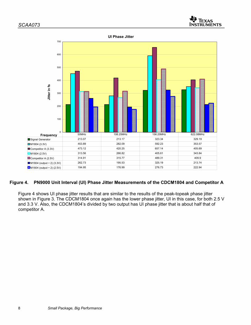
UI Phase Jitter
0
100
200
300
400
500
600
700
Frequency
Jitte
r in
fs
Signal Generator 213.07 213.17 323.34 329.19
M1804 (3.3V) 453.89 282.09 592.23 353.57
Competitor A (3.3V) 473.12 420.25 657.14 405.69
M1804 (2.5V) 313.56 266.82 405.61 343.84
Competitor A (2.5V) 314.91 315.77 489.31 409.9
M1804 (output ÷ 2) (3.3V) 262.73 195.53 325.19 213.74
M1804 (output ÷ 2) (2.5V) 194.95 176.99 276.73 222.94
50MHz 106.25MHz 156.25MHz 622.08MHz
Figure 4. PN9000 Unit Interval (UI) Phase Jitter Measurements of the CDCM1804 and Competitor A
Figure 4 shows UI phase jitter results that are similar to the results of the peak-topeak phase jitter shown in Figure 3. The CDCM1804 once again has the lower phase jitter, UI in this case, for both 2.5 V and 3.3 V. Also, the CDCM1804’s divided by two output has UI phase jitter that is about half that of competitor A.
SCAA073
Small Package, Big Performance 9
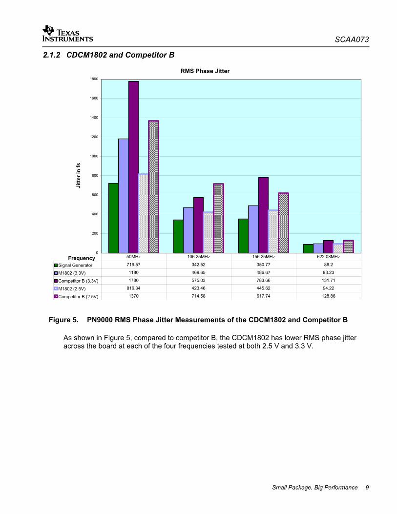
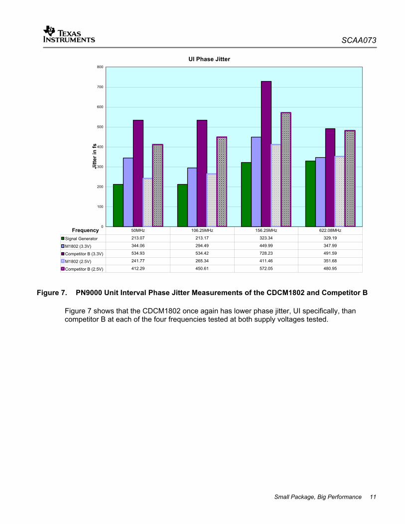
2.1.2 CDCM1802 and Competitor B
RMS Phase Jitter
0
200
400
600
800
1000
1200
1400
1600
1800
Frequency
Jitte
r in
fs
Signal Generator 719.57 342.52 350.77 88.2
M1802 (3.3V) 1180 469.65 486.67 93.23
Competitor B (3.3V) 1780 575.03 783.66 131.71
M1802 (2.5V) 816.34 423.46 445.62 94.22
Competitor B (2.5V) 1370 714.58 617.74 128.86
50MHz 106.25MHz 156.25MHz 622.08MHz
Figure 5. PN9000 RMS Phase Jitter Measurements of the CDCM1802 and Competitor B
As shown in Figure 5, compared to competitor B, the CDCM1802 has lower RMS phase jitter across the board at each of the four frequencies tested at both 2.5 V and 3.3 V.

SCAA073
10 Small Package, Big Performance
PP Phase Jitter
0
2
4
6
8
10
Frequency
Jitte
r in
fs
Signal Generator 4.26 2.01 2.07 0.52918
M1802 (3.3V) 6.88 2.77 2.88 0.5594
Competitor B (3.3V) 10.7 3.42 4.66 0.79024
M1802 (2.5V) 4.84 2.5 2.63 0.56533
Competitor B (2.5V) 8.25 4.24 3.66 0.77313
50MHz 106.25MHz 156.25MHz 622.08MHz
Figure 6. PN9000 Peak-to-Peak Phase Jitter Measurements of the CDCM1802 and Competitor B
The CDCM1802 again consistently has lower phase jitter, peak-to-peak in the above graph, than competitor B regardless of the frequency or supply voltage tested.
SCAA073
Small Package, Big Performance 11
UI Phase Jitter
0
100
200
300
400
500
600
700
800
Frequency
Jitte
r in
fs
Signal Generator 213.07 213.17 323.34 329.19
M1802 (3.3V) 344.06 294.49 449.99 347.99
Competitor B (3.3V) 534.93 534.42 728.23 491.59
M1802 (2.5V) 241.77 265.34 411.46 351.68
Competitor B (2.5V) 412.29 450.61 572.05 480.95
50MHz 106.25MHz 156.25MHz 622.08MHz
Figure 7. PN9000 Unit Interval Phase Jitter Measurements of the CDCM1802 and Competitor B
Figure 7 shows that the CDCM1802 once again has lower phase jitter, UI specifically, than competitor B at each of the four frequencies tested at both supply voltages tested.

SCAA073
12 Small Package, Big Performance
3 Summary When choosing a clock buffer for a system with a timing budget requirement, the choice must be made carefully. The CDCM1804 meets SONET jitter requirements at both 2.5 V and 3.3 V. The CDCM1804 also has lower peak-to-peak and UI phase jitters than competitor A at both 2.5 V and 3.3 V at each frequency tested. The majority of the RMS phase jitter measurements of the CDCM1804 are also lower than those of competitor A. The CDCM1804’s lower phase jitter gives more leeway in the timing budget. In addition, the CDCM1804 offers a 54 mode programmable divide. When the CDCM1804 was tested with the output divided by two, the phase jitter was approximately divided in half. Furthermore, the CDCM1804 has a LVCMOS output that can aid in the reduction of ICs necessary and board size.
The jitter measurements presented in this report show that the CDCM1802 meets the SONET RMS jitter requirement at each frequency tested at 2.5 V and at the three highest frequencies tested at 3.3 V. The CDCM1802 consistently has lower phase jitter than its competitor. Given the importance of the timing budget, the CDCM1802 is the more favorable choice as it outperforms competitor B at both 2.5 V and 3.3 V at each frequency tested. The CDCM1802 also has a LVCMOS output and an 11 mode programmable divide.
The low phase noise/phase jitter of the CDCM1804 and CDCM1802 make them ideal for applications in both telecom and datacom. Existing designs include but are not limited to: backplanes, medical imaging, and basestations. The CDCM1804 and CDCM1802 are also good solutions for driving DACs and ADCs including, DAC56xx, ADS55xx, and TLK/SLK product lines from Texas Instruments. Detailed phase noise plots of the devices tested at common frequencies are included in Appendix A.

SCAA073
Small Package, Big Performance 13
Appendix A.
Figure 8. Phase Noise Plots of the CDCM1804 and Competitor A at 50 MHz, 3.3 V
Figure 9. Phase Noise Plots of the CDCM1804 and Competitor A at 106.25 MHz, 3.3 V

SCAA073
14 Small Package, Big Performance
Figure 10. Phase Noise Plots of the CDCM1804 and Competitor A at 156.25 MHz, 3.3 V
Figure 11. Phase Noise Plots of the CDCM1804 and Competitor A at 622.08 MHz, 3.3 V
SCAA073
Small Package, Big Performance 15
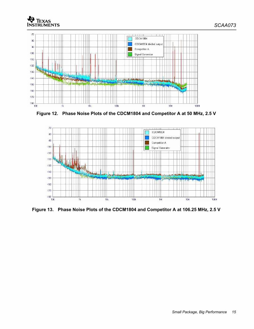
Figure 12. Phase Noise Plots of the CDCM1804 and Competitor A at 50 MHz, 2.5 V
Figure 13. Phase Noise Plots of the CDCM1804 and Competitor A at 106.25 MHz, 2.5 V

SCAA073
16 Small Package, Big Performance
Figure 14. Phase Noise Plots of the CDCM1804 and Competitor A at 156.25 MHz, 2.5 V
Figure 15. Phase Noise Plots of the CDCM1804 and Competitor A at 622.08 MHz, 2.5 V

SCAA073
Small Package, Big Performance 17
Figure 16. Phase Noise Plots of the CDCM1802 and Competitor B at 50 MHz, 3.3 V
Figure 17. Phase Noise Plots of the CDCM1802 and Competitor B at 106.25 MHz, 3.3 V

SCAA073
18 Small Package, Big Performance
Figure 18. Phase Noise Plots of the CDCM1802 and Competitor B at 156.25 MHz, 3.3 V
Figure 19. Phase Noise Plots of the CDCM1802 and Competitor B at 622.08 MHz, 3.3 V

SCAA073
Small Package, Big Performance 19
Figure 20. Phase Noise Plots of the CDCM1802 and Competitor B at 50 MHz, 2.5 V
Figure 21. Phase Noise Plots of the CDCM1802 and Competitor B at 106.25 MHz, 2.5 V

SCAA073
20 Small Package, Big Performance
Figure 22. Phase Noise Plots of the CDCM1802 and Competitor B at 156.25 MHz, 2.5 V
Figure 23. Phase Noise Plots of the CDCM1802 and Competitor B at 622.08 MHz, 2.5 V
References 1. CDCM1804 data sheet, Texas Instruments, (SCAS697) 2. CDCM1802 data sheet, Texas Instruments, (SCAS759) 3. DC-Coupling Between Differential LVPECL, LVDS, HSTL, and CML, Texas Instruments
application report, (SCAA062) 4. AC-Coupling Between LVPECL, LVDS, CML, and HSTL, Texas Instruments application
report, (SCAA059) 5. Advantage of Using Texas Instruments Lowest Jitter Differential Clock Buffer, Texas
Instruments application report, (SCAA068) 6. Benefits of Using Texas Instruments Non-PLL Clock Buffer: Best in Class Phase
Noise/Phase, Texas Instruments application report, (SCAA066)

IMPORTANT NOTICE
Texas Instruments Incorporated and its subsidiaries (TI) reserve the right to make corrections, modifications,enhancements, improvements, and other changes to its products and services at any time and to discontinueany product or service without notice. Customers should obtain the latest relevant information before placingorders and should verify that such information is current and complete. All products are sold subject to TI’s termsand conditions of sale supplied at the time of order acknowledgment.
TI warrants performance of its hardware products to the specifications applicable at the time of sale inaccordance with TI’s standard warranty. Testing and other quality control techniques are used to the extent TIdeems necessary to support this warranty. Except where mandated by government requirements, testing of allparameters of each product is not necessarily performed.
TI assumes no liability for applications assistance or customer product design. Customers are responsible fortheir products and applications using TI components. To minimize the risks associated with customer productsand applications, customers should provide adequate design and operating safeguards.
TI does not warrant or represent that any license, either express or implied, is granted under any TI patent right,copyright, mask work right, or other TI intellectual property right relating to any combination, machine, or processin which TI products or services are used. Information published by TI regarding third-party products or servicesdoes not constitute a license from TI to use such products or services or a warranty or endorsement thereof.Use of such information may require a license from a third party under the patents or other intellectual propertyof the third party, or a license from TI under the patents or other intellectual property of TI.
Reproduction of information in TI data books or data sheets is permissible only if reproduction is withoutalteration and is accompanied by all associated warranties, conditions, limitations, and notices. Reproductionof this information with alteration is an unfair and deceptive business practice. TI is not responsible or liable forsuch altered documentation.
Resale of TI products or services with statements different from or beyond the parameters stated by TI for thatproduct or service voids all express and any implied warranties for the associated TI product or service andis an unfair and deceptive business practice. TI is not responsible or liable for any such statements.
Following are URLs where you can obtain information on other Texas Instruments products and applicationsolutions:
Products Applications
Amplifiers amplifier.ti.com Audio www.ti.com/audio
Data Converters dataconverter.ti.com Automotive www.ti.com/automotive
DSP dsp.ti.com Broadband www.ti.com/broadband
Interface interface.ti.com Digital Control www.ti.com/digitalcontrol
Logic logic.ti.com Military www.ti.com/military
Power Mgmt power.ti.com Optical Networking www.ti.com/opticalnetwork
Microcontrollers microcontroller.ti.com Security www.ti.com/security
Telephony www.ti.com/telephony
Video & Imaging www.ti.com/video
Wireless www.ti.com/wireless
Mailing Address: Texas Instruments
Post Office Box 655303 Dallas, Texas 75265
Copyright 2004, Texas Instruments Incorporated