Embed Size (px)
Citation preview

1
2
3
4
5
6
7
8
9
10
11
12
UCC28950
DCM
RSUM
RT
TMIN
DELEF
DELCD
DELAB
SS/EN
COMP
EA-
EA+
VREF 24
23
22
21
20
19
18
17
16
15
14
13ADELEF
ADEL
CS
SYNC
OUTF
OUTE
OUTD
OUTC
OUTB
OUTA
VDD
GND
RDCM(hi)
RDCM
RCS
R7
RA(hi)
RAEF(hi)
RAEF
RA
A
B
C
D
E
F
CVDD
VDD
SYNC
VREF
R5C2
C1
R4
R3
CREF
R2R1
VSENSE
ENABLE
+
-
CT
A
VDD
B
VDD
QA
QB
C
VDD
D
VDD
QC
QD
QE QFE F
VOUT
+
-
VSENSE
UCC27324 UCC27324
C3R6C
SS
RAB
RCD
REF
RTMIN
RT
RSUM
Voltage Current
Sense
VREF
UCC28950
www.ti.com SLUSA16 –MARCH 2010
Green Phase-Shifted Full-Bridge Controller With Synchronous RectificationCheck for Samples: UCC28950
1FEATURES APPLICATIONS• Phase-Shifted Full-Bridge Converters• Enhanced Wide Range Resonant Zero Voltage
Switching (ZVS) Capability • Server, Telecom Power Supplies• Industrial Power Systems• Direct Synchronous Rectifier (SR) Control• High-Density Power Architectures• Light-Load Efficiency Management Including• Solar Inverters, and Electric Vehicles– Burst Mode Operation
– Discontinuous Conduction Mode (DCM), DESCRIPTIONDynamic SR On/Off Control withProgrammable Threshold The UCC28950 enhanced phase-shifted controller
builds upon Texas Instrument’s industry standard– Programmable Adaptive DelayUCCx895 phase-shifted controller family with
• Average or Peak Current Mode Control with enhancements that offer best in class efficiency inProgrammable Slope Compensation and today’s high performance power systems. TheVoltage Mode Control UCC28950 implements advanced control of the
full-bridge along with active control of the• Closed Loop Soft Start and Enable Functionsynchronous rectifier output stage.• Programmable Switching Frequency up to 1
MHz with Bi-Directional Synchronization The primary-side signals allow programmable delaysto ensure ZVS operation over wide-load current and• (+/-3%) Cycle-by-Cycle Current Limitinput voltage range, while the load current naturallyProtection with Hiccup Mode Supporttunes the secondary-side synchronous rectifiers
• 150-µA Start-Up Current switching delays, maximizing overall system• VDD Under Voltage Lockout efficiency.• Wide Temperature Range -40°C to 125°C
UCC28950 Typical Application
1
Please be aware that an important notice concerning availability, standard warranty, and use in critical applications of TexasInstruments semiconductor products and disclaimers thereto appears at the end of this data sheet.
PRODUCTION DATA information is current as of publication date. Copyright © 2010, Texas Instruments IncorporatedProducts conform to specifications per the terms of the TexasInstruments standard warranty. Production processing does notnecessarily include testing of all parameters.

UCC28950
SLUSA16 –MARCH 2010 www.ti.com
DESCRIPTION (CONT.)The UCC28950 also offers multiple light-load management features including burst mode and dynamic SR on/offcontrol when transitioning in and out of Discontinuous Current Mode (DCM) operation, ensuring ZVS operation isextended down to much lighter loads.
In addition, the UCC28950 includes support for peak current along with voltage mode control, programmableswitching frequency up to 1 MHz and a wide set of protection features including cycle-by-cycle current limit,UVLO and thermal shutdown. A 90-degree phase-shifted interleaved synchronized operation can be easilyarranged between two converters.
The UCC28950 is available in TSSOP-24 package.
ORDERING INFORMATIONTEMPERATURE RANGE, TA = PACKAGE TAPE AND REEL QTY. PART NUMBERTJ
250 UCC28950PW-40°C to 125°C Plastic 24-pin TSSOP (PW)
2000 UCC28950PWTR
ABSOLUTE MAXIMUM RATINGSover operating free-air temperature range (unless otherwise noted) (1) (2)
PARAMETER VALUE UNIT
Input supply voltage range, VDD(3) -0.4 to 20.0
OUTA, OUTB, OUTC, OUTD, OUTE, OUTF -0.4 to VDD + 0.4
Inputs voltages on DELAB, DELCD, DELEF, SS/EN, DCM, TMIN, RT, SYNC, RSUM, EA+, EA-, -0.4 to VREF +COMP, CS, ADEL, ADELEF 0.4 VOutput voltage on VREF -0.4 to 5.6
ESD rating, HBM 2 k
ESD rating, CDM 500
Continuous total power dissipation See dissipation rating table
Operating virtual junction temperature range, TJ -40 to 150
Operating ambient temperature range, TA -40 to 125°C
Storage temperature, Tstg -65 to 150
Lead temperature (soldering, 10 sec.) 300
(1) Stresses beyond those listed under “absolute maximum ratings” may cause permanent damage to the device. These are stress ratingsonly, and functional operation of the device at these or any other conditions beyond those indicated under “recommended operatingconditions” is not implied. Exposure to absolute-maximum-rated conditions for extended periods may affect device reliability.
(2) These devices are sensitive to electrostatic discharge; follow proper device handling procedures.(3) All voltages are with respect to GND unless otherwise noted. Currents are positive into, negative out of the specified terminal. See
Packaging Section of the datasheet for thermal limitations and considerations of packages.
DISSIPATION RATINGS (1)
DERATING POWER RATINGFACTORRqJC RqJAPACKAGE (°C/W) (°C/W) ABOVE TA = TA < 25°C TA = 70°C TA = 85°C25°C
PW 18.5 89.3 11.2 mW/ °C 1.12 W 0.615 W 0.448 W
(1) These thermal data are taken at standard JEDEC test conditions and are useful for the thermal performance comparison of differentpackages. The cooling condition and thermal impedance RqJA of practical design is specific.
2 Submit Documentation Feedback Copyright © 2010, Texas Instruments Incorporated
Product Folder Link(s): UCC28950

UCC28950
www.ti.com SLUSA16 –MARCH 2010
RECOMMENDED OPERATING CONDITIONSover operating free-air temperature range (unless otherwise noted)
MIN TYP MAX UNIT
Supply voltage range, VDD 8 12 17 V
Operating junction temperature range -40 125 °C
Converter switching frequency setting range, FSW(nom) 50 1000 kHz
Programmable delay range between OUTA, OUTB and OUTC, OUTD set by 30 1400resistors DELAB and DELCD and parameter KA(1)
nsProgrammable delay range between OUTA, OUTF and OUTB, OUTE set by 30 1400resistor DELEF, and parameter KEF
(1)
Programmable DCM range as percentage of voltage at CS (1) 5% 30%
Programmable TMIN range 100 800 ns
(1) Verified during characterization only.
ELECTRICAL CHARACTERISTICS (1)
VDD = 12 V, TA = TJ = -40°C to 125°C, CVDD = 1 µF, CREF = 1 µF, RAB = 22.6 kΩ, RCD = 22.6 kΩ , REF = 13.3 kΩ, RSUM = 124kΩ, RMIN = 88.7 kΩ, RT = 59 kΩ connected between RT pin and 5-V voltage supply to set FSW = 100 kHz (FOSC = 200 kHz)(unless otherwise noted). All component designations are from the Typical Application Diagram.
PARAMETER TEST CONDITION MIN TYP MAX UNITS
Under Voltage Lockout (UVLO)
UVLO_R Start threshold 6.75 7.3 7.9TH
UVLO_F Minimum operating voltage 6.15 6.7 7.2 VTH after start
UVLO_H Hysteresis 0.53 0.6 0.75YST
Supply Currents
IDD(off) Startup current VDD is 5.2 V 150 270 µA
IDD Operating supply current 5 10 mA
VREF Output Voltage
VREF VREF total output range 0 ≤ IR ≤ 20 mA; VDD = from 8 V to 17 V 4.925 5 5.075 V
ISCC Short circuit current VREF = 0 V -53 -23 mA
Switching Frequency (½ of internal oscillator frequency FOSC)
FSW(nom) Total range 92 100 108 KHz
DMAX Maximum duty cycle 95% 97%
Synchronization
RT = 59 kΩ between RT and GND; Input pulsesPHSYNC Total range 85 90 95 °PH200 kHz, D = 0.5 at SYNC
RT = 59 kΩ between RT and 5 V; -40 °C ≤ TJ ≤FSYNC Total range 180 200 220 kHz125°C
TPW Pulse width 2.2 2.5 2.8 µs
(1) Typical values for TA = 25°C
Copyright © 2010, Texas Instruments Incorporated Submit Documentation Feedback 3
Product Folder Link(s): UCC28950

UCC28950
SLUSA16 –MARCH 2010 www.ti.com
ELECTRICAL CHARACTERISTICS (1) (continued)VDD = 12 V, TA = TJ = -40°C to 125°C, CVDD = 1 µF, CREF = 1 µF, RAB = 22.6 kΩ, RCD = 22.6 kΩ , REF = 13.3 kΩ, RSUM = 124kΩ, RMIN = 88.7 kΩ, RT = 59 kΩ connected between RT pin and 5-V voltage supply to set FSW = 100 kHz (FOSC = 200 kHz)(unless otherwise noted). All component designations are from the Typical Application Diagram.
PARAMETER TEST CONDITION MIN TYP MAX UNITS
Error Amplifier
VICM range ensures parameters, the functionalityCommon mode input voltageVICM ensured for 3.6 V < VICM < VREF + 0.4 V, and -0.4 0.5 3.6 Vrange V < VICM < 0.5 V
VIO Offset voltage - 7 7 mV
IBIAS Input bias current -1 1 µA
EAHIGH High-level output voltage (EA+) - (EA-) = 500 mV, IEAOUT = -0.5 mA 3.9 4.25V
EALOW Low-level output voltage (EA+) - (EA-) = -500 mV, IEAOUT = 0.5 mA 0.25 0.35
ISOURCE Error amplifier source current -8 -3.75 -0.5mA
ISINK Error amplifier sink current 2.7 4.6 5.75
IVOL Open-loop dc gain 100 dB
GBW Unity gain bandwidth (2) 3 MHz
Cycle-by-Cycle Current Limit
CS pin cycle-by-cycleVCS_LIM 1.94 2 2.06 Vthreshold
Propagation delay from CS to Input pulse between CS and GND from zero to 2.5TCS 100 nsOUTC and OUTD outputs V
Internal Hiccup Mode Settings
Discharge current to setIDS cycle-by-cycle current limit CS = 2.5 V, VSS = 4 V 15 20 25 µA
duration
VHCC Hiccup OFF Time threshold 3.2 3.6 4.2 V
Discharge current to setIHCC 1.90 2.55 3.2 µAHiccup Mode OFF Time
Soft Start/Enable
ISS Charge current VSS = 0 V 20 25 30 µA
Shutdown/restart/resetVSS_STD 0.25 0.50 0.70thresholdVVSS_PU Pull up threshold 3.3 3.7 4.3
VSS_CL Clamp voltage 4.20 4.65 4.95
(2) Verified during characterization only.
4 Submit Documentation Feedback Copyright © 2010, Texas Instruments Incorporated
Product Folder Link(s): UCC28950
UCC28950
www.ti.com SLUSA16 –MARCH 2010
ELECTRICAL CHARACTERISTICS (1) (continued)VDD = 12 V, TA = TJ = -40°C to 125°C, CVDD = 1 µF, CREF = 1 µF, RAB = 22.6 kΩ, RCD = 22.6 kΩ , REF = 13.3 kΩ, RSUM = 124kΩ, RMIN = 88.7 kΩ, RT = 59 kΩ connected between RT pin and 5-V voltage supply to set FSW = 100 kHz (FOSC = 200 kHz)(unless otherwise noted). All component designations are from the Typical Application Diagram.
PARAMETER TEST CONDITION MIN TYP MAX UNITS
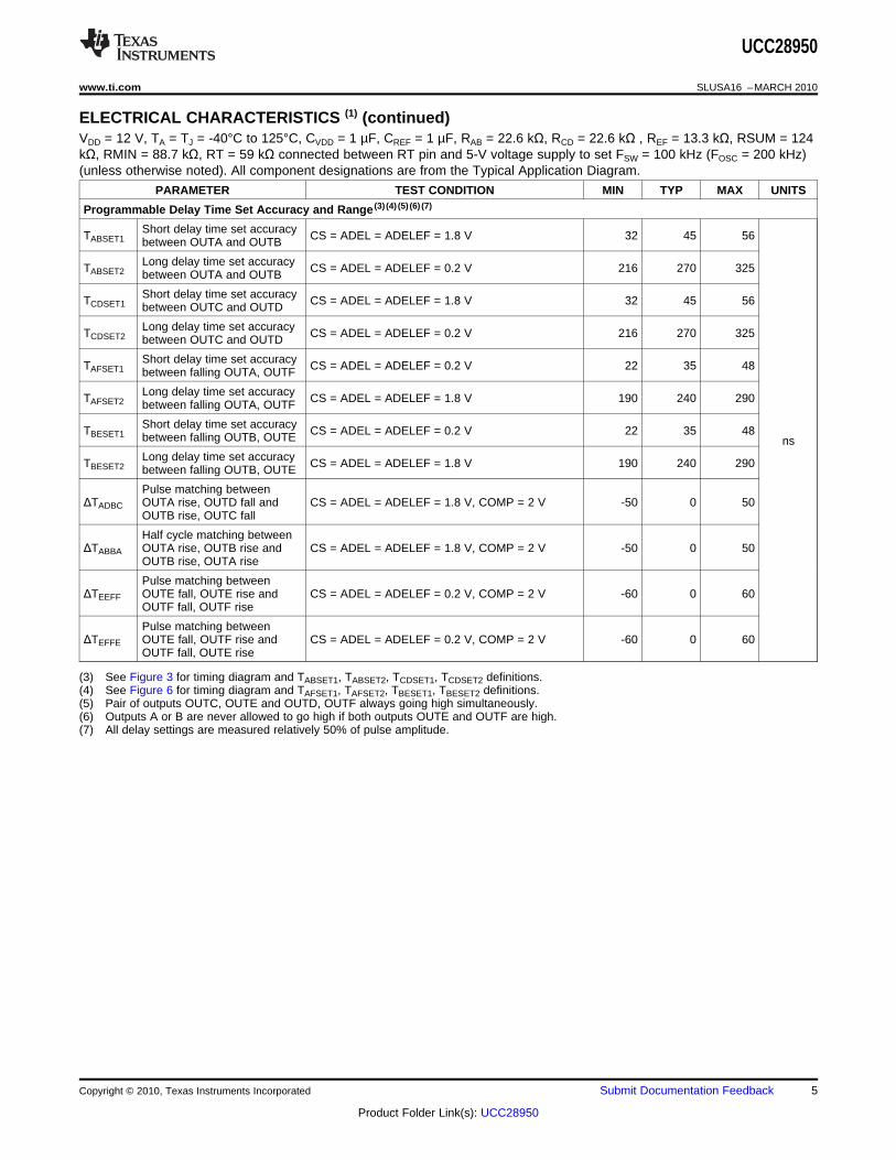
Programmable Delay Time Set Accuracy and Range (3) (4) (5) (6) (7)
Short delay time set accuracyTABSET1 CS = ADEL = ADELEF = 1.8 V 32 45 56between OUTA and OUTB
Long delay time set accuracyTABSET2 CS = ADEL = ADELEF = 0.2 V 216 270 325between OUTA and OUTB
Short delay time set accuracyTCDSET1 CS = ADEL = ADELEF = 1.8 V 32 45 56between OUTC and OUTD
Long delay time set accuracyTCDSET2 CS = ADEL = ADELEF = 0.2 V 216 270 325between OUTC and OUTD
Short delay time set accuracyTAFSET1 CS = ADEL = ADELEF = 0.2 V 22 35 48between falling OUTA, OUTF
Long delay time set accuracyTAFSET2 CS = ADEL = ADELEF = 1.8 V 190 240 290between falling OUTA, OUTF
Short delay time set accuracyTBESET1 CS = ADEL = ADELEF = 0.2 V 22 35 48between falling OUTB, OUTE nsLong delay time set accuracyTBESET2 CS = ADEL = ADELEF = 1.8 V 190 240 290between falling OUTB, OUTE
Pulse matching betweenΔTADBC OUTA rise, OUTD fall and CS = ADEL = ADELEF = 1.8 V, COMP = 2 V -50 0 50
OUTB rise, OUTC fall
Half cycle matching betweenΔTABBA OUTA rise, OUTB rise and CS = ADEL = ADELEF = 1.8 V, COMP = 2 V -50 0 50
OUTB rise, OUTA rise
Pulse matching betweenΔTEEFF OUTE fall, OUTE rise and CS = ADEL = ADELEF = 0.2 V, COMP = 2 V -60 0 60
OUTF fall, OUTF rise
Pulse matching betweenΔTEFFE OUTE fall, OUTF rise and CS = ADEL = ADELEF = 0.2 V, COMP = 2 V -60 0 60
OUTF fall, OUTE rise
(3) See Figure 3 for timing diagram and TABSET1, TABSET2, TCDSET1, TCDSET2 definitions.(4) See Figure 6 for timing diagram and TAFSET1, TAFSET2, TBESET1, TBESET2 definitions.(5) Pair of outputs OUTC, OUTE and OUTD, OUTF always going high simultaneously.(6) Outputs A or B are never allowed to go high if both outputs OUTE and OUTF are high.(7) All delay settings are measured relatively 50% of pulse amplitude.
Copyright © 2010, Texas Instruments Incorporated Submit Documentation Feedback 5
Product Folder Link(s): UCC28950
UCC28950
SLUSA16 –MARCH 2010 www.ti.com
ELECTRICAL CHARACTERISTICS (1) (continued)VDD = 12 V, TA = TJ = -40°C to 125°C, CVDD = 1 µF, CREF = 1 µF, RAB = 22.6 kΩ, RCD = 22.6 kΩ , REF = 13.3 kΩ, RSUM = 124kΩ, RMIN = 88.7 kΩ, RT = 59 kΩ connected between RT pin and 5-V voltage supply to set FSW = 100 kHz (FOSC = 200 kHz)(unless otherwise noted). All component designations are from the Typical Application Diagram.
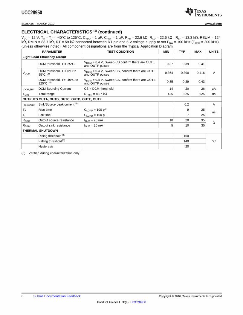
PARAMETER TEST CONDITION MIN TYP MAX UNITS
Light Load Efficiency Circuit
VDCM = 0.4 V, Sweep CS confirm there are OUTEDCM threshold, T = 25°C 0.37 0.39 0.41and OUTF pulses
DCM threshold, T = 0°C to VDCM = 0.4 V, Sweep CS, confirm there are OUTEVDCM 0.364 0.390 0.416 V85°C (8) and OUTF pulses
DCM threshold, T= -40°C to VDCM = 0.4 V, Sweep CS, confirm there are OUTE 0.35 0.39 0.43125°C (8) and OUTF pulses
IDCM,SRC DCM Sourcing Current CS < DCM threshold 14 20 26 µA
TMIN Total range RTMIN = 88.7 kΩ 425 525 625 ns
OUTPUTS OUTA, OUTB, OUTC, OUTD, OUTE, OUTF
ISINK/SRC Sink/Source peak current (8) 0.2 A
TR Rise time CLOAD = 100 pF 9 25ns
TF Fall time CLOAD = 100 pF 7 25
RSRC Output source resistance IOUT = 20 mA 10 20 35Ω
RSINK Output sink resistance IOUT = 20 mA 5 10 30
THERMAL SHUTDOWN
Rising threshold (8) 160
Falling threshold (8) 140 °C
Hysteresis 20
(8) Verified during characterization only.
6 Submit Documentation Feedback Copyright © 2010, Texas Instruments Incorporated
Product Folder Link(s): UCC28950

1
2
3
4
5
6
7
8
9
10
11
12
UCC28950
DCM
RSUM
RT
TMIN
DELEF
DELCD
DELAB
SS/EN
COMP
EA-
EA+
VREF 24
23
22
21
20
19
18
17
16
15
14
13ADELEF
ADEL
CS
SYNC
OUTF
OUTE
OUTD
OUTC
OUTB
OUTA
VDD
GND
UCC28950
www.ti.com SLUSA16 –MARCH 2010
DEVICE INFORMATION
Plastic 24-pin TSSOP (PW)
TERMINAL FUNCTIONSTERMINAL
I/O FUNCTIONNUMBER NAME
1 VREF O 5-V, ±1.5%, 20-mA reference voltage output.
2 EA+ I Error amplifier non-inverting input.
3 EA- I Error amplifier inverting input.
4 COMP I/O Error amplifier output and input to the PWM comparator.
5 SS/EN I Soft-start programming, device enable and hiccup mode protection circuit.
6 DELAB I Dead-time delay programming between OUTA and OUTB.
7 DELCD I Dead-time delay programming between OUTC and OUTD.
8 DELEF I Delay-time programming between OUTA to OUTF, and OUTB to OUTE.
9 TMIN I Minimum duty cycle programming in burst mode.
10 RT I Oscillator frequency set. Master or slave mode setting.
11 RSUM I Slope compensation programming. Voltage mode or peak current mode setting.
12 DCM I DCM threshold setting.
Delay-time programming between primary side and secondary side switches, TAFSET13 ADELEF I and TBESET.
Dead-time programming for the primary switches over CS voltage range, TABSET and14 ADEL I TCDSET.
15 CS I Current sense for cycle-by-cycle over-current protection and adaptive delay functions.
16 SYNC I/O Synchronization out from Master controller to input of slave controller.
17 OUTF O 0.2-A sink/source synchronous switching output.
18 OUTE O 0.2-A sink/source synchronous switching output.
19 OUTD O 0.2-A sink/source primary switching output.
20 OUTC O 0.2-A sink/source primary switching output.
21 OUTB O 0.2-A sink/source primary switching output.
22 OUTA O 0.2-A sink/source primary switching output.
23 VDD I Bias supply input.
24 GND Ground. All signals are referenced to this node.
Copyright © 2010, Texas Instruments Incorporated Submit Documentation Feedback 7
Product Folder Link(s): UCC28950
EN
Thermal
Shutdown
5V LDO
+
VDD
23VDD
UVLO
COMP
VDD
1VREF
Reference
Generator
VDD
ON/OFF7.3 V Rise
6.7 V Fall
+
-
Programmable
Delay AB
22 OUTA
6 DELAB
21 OUTB
14
ADEL
Programmable
Delay CD
20 OUTC
7 DELCD
19 OUTD
Programmable
Delay EF
18 OUTE
8 DELEF
17 OUTF
13 ADELEF
Soft Stat and Enable
with 0.55 V Threshold
17
OUTF
Light-Load
Efficiency Block
+
4COMP
++
3
2
EA-
EA+
Oscillator
Lower "+" Input
is Dominant
10RT
Ramp
Summing11RSUM
15CS
CS
Synchronization
Block
15
CS
+
+
-
24
GND
CS
12
DCM
9
TMIN
Logic Block
PWM
COMP
Cycle-by-Cycle
ILIM
2 V
2.8 V
0.8 V
RAMP
CLK
1
2
3
4
5
6
7
8
9
10
11
12
UCC28950
DCM
RSUM
RT
TMIN
DELEF
DELCD
DELAB
SS/EN
COMP
EA-
EA+
VREF 24
23
22
21
20
19
18
17
16
15
14
13ADELEF
ADEL
CS
SYNC
OUTF
OUTE
OUTD
OUTC
OUTB
OUTA
VDD
GND
RDCM(hi)
RDCM
RCS
R7
RA(hi)
RAEF(hi)
RAEF
RA
A
B
C
D
E
F
CVDD
VDD
SYNC
VREF
R5C2
C1
R4
R3
CREF
R2R1
VSENSE
ENABLE
+
-
CT
A
VDD
B
VDD
QA
QB
C
VDD
D
VDD
QC
QD
QE QFE F
VOUT
+
-
VSENSE
UCC27324 UCC27324
C3R6C
SS
RAB
RCD
REF
RTMIN
RT
RSUM
Voltage Current
Sense
VREF
UCC28950
SLUSA16 –MARCH 2010 www.ti.com
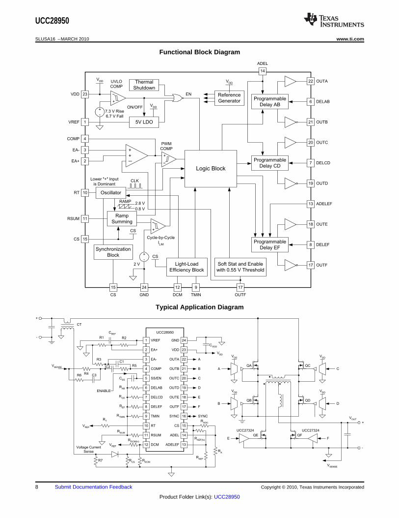
Functional Block Diagram
Typical Application Diagram
8 Submit Documentation Feedback Copyright © 2010, Texas Instruments Incorporated
Product Folder Link(s): UCC28950

VDD
VDD_GOOD
7.3V rise, 6.7V fall
VREF
VREF_GOOD
CLK
TMIN
RAMP
PWM
SS>0.5V, then Release COMP, DCM, CS, Outputs A, B, C, D, E, F
No PWM pulses shorter
than TMIN except
during cycle-by-cycle
curr. limit
TMIN
A
B
C
D
E
F
4.8V rise, 4.6V fall
2Vp-p
Add 0.85V offset to RAMP and COMP
PWMCOMPTMIN
2Vp-p
UCC28950
www.ti.com SLUSA16 –MARCH 2010
Startup Timing Diagram
No output delay shown, COMP-to-RAMP offset not included.
Figure 1. UCC28950 Timing Diagram
NOTEThere is no pulse on OUTE during burst mode at startup. Two falling edge PWM pulsesare required before enabling the synchronous rectifier outputs.
Copyright © 2010, Texas Instruments Incorporated Submit Documentation Feedback 9
Product Folder Link(s): UCC28950

VDD
VDD_GOOD
VREF
VREF_GOOD
CLK
TMIN
No PWM pulses shorter than TMIN except
during cycle-by-cycle current limit
A
B
C
D
E
F
7.3V rise, 6.7V fall
4.8V rise, 4.6V fall
TMIN
VDD failed and VDD_GOOD goes low,
Everything is shutdown
RAMP 2Vp-pCOMP
PWM
Add 0.85V offset to RAMP and COMP
UCC28950
SLUSA16 –MARCH 2010 www.ti.com
Steady State/Shutdown Timing Diagram
No output delay shown, COMP-to-RAMP offset not included.
Figure 2. UCC28950 Timing Diagram
10 Submit Documentation Feedback Copyright © 2010, Texas Instruments Incorporated
Product Folder Link(s): UCC28950

UCC28950
www.ti.com SLUSA16 –MARCH 2010
DETAILED PIN DESCRIPTION AND PARAMETER SETTINGS
Start-Up Protection Logic
Before the UCC28950 controller will start up, the following conditions must be met:• VDD voltage exceeds rising UVLO threshold 7.3 V typical.• The 5-V reference voltage is available.• Junction temperature is below the thermal shutdown threshold of 140°C.• The voltage on the soft-start capacitor is not below 0.55 V typical.
If all those conditions are met, an internal enable signal EN is generated that initiates the soft start process. Theduty cycle during the soft start is defined by the voltage at the SS pin, and cannot be lower than the duty cycleset by TMIN, or by cycle-by-cycle current limit circuit depending on load conditions.
Voltage Reference (VREF)
The accurate (±1.5%) 5-V reference voltage regulator with the short circuit protection circuit supplies internalcircuitry and provides up to 20-mA external output current for setting DC/DC converter parameters. Place lowESR and ESL, preferably ceramic decoupling capacitor CREF in 1 µF to 2.2 µF range from this pin to GND asclose to the related pins as possible for best performance. The only condition where the reference regulator isshut down internally is during under voltage lockout.
Error Amplifier (EA+, EA-, COMP)
The error amplifier has two uncommitted inputs, EA+ and EA-, with a 3-MHz unity bandwidth, which allowsflexibility in closing the feedback loop. The EA+ is a non-inverting input, the EA- is an inverting input and theCOMP is the output of the error amplifier. The input voltage common mode range, where the parameters of erroramplifier are guaranteed, is from 0.5 V to 3.6 V. The output of the error amplifier is connected internally to thenon-inverting input of the PWM comparator. The range of the error amplifier output of 0.25 V to 4.25 V farexceeds the PWM comparator input ramp-signal range, which is from 0.8 V to 2.8 V. The soft-start signal servesas an additional non-inverting input of the error amplifier. The lower of the two non-inverting inputs of the erroramplifier is the dominant input and sets the duty cycle where the output signal of the error amplifier is comparedwith the internal ramp at the inputs of the PWM comparator.
Copyright © 2010, Texas Instruments Incorporated Submit Documentation Feedback 11
Product Folder Link(s): UCC28950

( )SS
SS(master )
T 25 AC
VNI 0.55
´ m=
+
SSSS(slave)
TC
20.6825K Ln
20.6 VNI 0.55
=æ ö
´ ç ÷- -è ø
UCC28950
SLUSA16 –MARCH 2010 www.ti.com
Soft Start and Enable (SS/EN)
The soft-start pin SS/EN is a multi-function pin used for the following operations:• Closed loop soft start with the gradual duty cycle increase from the minimum set by TMIN up to the steady
state duty cycle required by the regulated output voltage.• Setting hiccup mode conditions during cycle-by-cycle over current limit.• On/off control for the converter.
During soft start, one of the voltages at the SS/EN or EA+ pins, whichever is lower (SS/EN - 0.55 V) or EA+voltage (see Block Diagram), sets the reference voltage for a closed feedback loop. Both SS/EN and EA+ signalsare non-inverting inputs of the error amplifier with the COMP pin being its output. Thus the soft start always goesunder the closed feedback loop and the voltage at COMP pin sets the duty cycle. The duty cycle defined byCOMP voltage can not be shorter than TMIN pulse set by the user. However, if the shortest duty cycle is set bythe cycle-by-cycle current limit circuit, then it becomes dominant over the duty cycle defined by COMP voltage orby TMIN block.
The soft-start duration is defined by an external capacitor CSS, connected between SS/EN pin and ground, andthe internal charge current that has typical value of 25 µA. Pulling the soft-start pin externally below 0.55 V shutsdown the controller. The release of the soft-start pin enables the controller to start, and if there is no current limitcondition, the duty cycle applied to the output inductor gradually increases until it reaches the steady state dutycycle defined by the regulated output voltage of the converter. This happens when the voltage at the SS/EN pinreaches and then exceeds the voltage at EA+ pin defined as VNI by 0.55 V. Thus for the given soft-start timeTSS, the CSS value can be defined by Equation 1 or Equation 2:
(1)
(2)
For example, in , if the soft-start time TSS is selected to be 10 ms, and the VNI is 2.5 V, then the soft-startcapacitor CSS is equal to 84 nF, an 82-nF capacitor can be used.
NOTEIf the converter is configured in Slave Mode, make sure you place an 825-kΩ resistor fromSS pin to ground.
Light-Load Power Saving Mode
The UCD28950 offers four different light-load management techniques for improving the efficiency of a powerconverter over a wide load current range.1. Adaptive Delay,
(a) ADEL, which sets and optimizes the dead-time control for the primary switches over wide load currentrange.
(b) ADELEF, which sets and optimizes the delay-time control between the primary side switches and thesecondary side switches.
2. TMIN, sets the minimum duty cycle as long as the part is not in current limit mode.3. Dynamic synchronous rectifier on/off control in DCM Mode, For increased efficiency at light loads. The DCM
Mode starts when the voltage at CS pin is lower than the threshold set by the user. In DCM Mode, thesynchronous output drive signals OUTE and OUTF are brought down low.
4. Burst Mode, for maximum efficiency at very light loads or no load. Burst Mode has an even number of PWMTMIN pulses followed by off time. Transition to the Burst Mode is defined by the TMIN duration set by theuser.
12 Submit Documentation Feedback Copyright © 2010, Texas Instruments Incorporated
Product Folder Link(s): UCC28950

OUTA
(OUTC)
OUTB
(OUTD)
TABSET1
TCDSET1
TABSET2
TCDSET2
TABSET2
TCDSET2
TABSET1
TCDSET1
UCC28950
www.ti.com SLUSA16 –MARCH 2010
Adaptive Delay, (Delay between OUTA and OUTB, OUTC and OUTD (DELAB, DELCD, ADEL))
The resistor RAB from the DELAB pin, DELAB to GND, along with the resistor divider RAHI from CS pin to ADELpin and RA from ADEL pin to GND sets the delay TABSET between one of outputs OUTA or OUTB going low andanother output going high Figure 3.
Figure 3. Delay definitions between OUTA and OUTB, OUTC and OUTD
This delay gradually increases as a function of the CS signal from TABSET1, which is measured at VCS = 1.8 V, toTABSET2, which is measured at the VCS = 0.2 V. This approach ensures there will be no shoot-through currentduring the high-side and low-side MOSFET switching and optimizes the delay for ZVS condition over a wide loadcurrent range. Depending on the resistor divider RAHI and RA, the proportional ratio between longest and shortestdelay is set. The max ratio is achieved by tying the CS and ADEL pins together. If ADEL is connected to GND,then the delay is fixed, defined only by the resistor RAB from DELAB to GND. The delay TCDSET1 and TCDSET2settings and their behaviour for outputs OUTC and OUTD are very similar to the one described for OUTA andOUTB. The difference is that resistor RCD connected between DELCD pin and GND sets the delay TCDSET.Delays for outputs OUTC and OUTD share with the outputs OUTA and OUTB the same CS voltage dependencepin ADEL.
Copyright © 2010, Texas Instruments Incorporated Submit Documentation Feedback 13
Product Folder Link(s): UCC28950

ABABSET
A
5 RT ns 5ns
0.15 V CS K 1.46
æ ö´= +ç ÷
+ ´ ´è ø
CDCDSET
A
5 RT ns 5ns
0.15 V CS K 1.46
æ ö´= +ç ÷
+ ´ ´è ø
AA
A AHI
RK
R R=
+
UCC28950
SLUSA16 –MARCH 2010 www.ti.com
The delay time TABSET is defined by the following Equation 3.
(3)
The same equation is used to define the delay time TCDSET in another leg except RAB is replaced by RCD.
(4)
In these equations RAB and RCD are in kΩ and CS, the voltage at pin CS, is in volts and KA is a numericalcoefficient in the range from 0 to 1. The delay time TABSET and TCDSET are in ns. These equations are empiricaland they are approximated from measured data. Thus, there is no unit agreement in the equations. As anexample, assume RAB = 15 kΩ, CS = 1 V and KA = 0.5. Then the TABSET is going to be 90.25 ns. In bothEquation 3 and Equation 4, KA is the same and is defined as:
(5)
KA sets how the delay is sensitive to CS voltage variation. If KA = 0 (ADEL shorted to GND), the delay is fixed. IfKA = 1 (ADEL is tied to CS), the delay is maximum at CS = 0.2 V and gradually decreases when CS goes up to1.8 V. The ratio between the maximum and minimum delay can be up to 6:1.
It is recommended to start by setting KA = 0 and set TABSET and TCDSET relatively large using equations or plots inthe data sheet to avoid hard switching or even shoot through current. The delay between outputs A, B and C, Dset by resistors RAB and RCS accordingly. Program the optimal delays at light load first. Then by changing KA setthe optimal delay for the outputs A, B at maximum current. KA for outputs C, D is the same as for A,D. Usuallyoutputs C, D always have ZVS if sufficient delay is provided.
NOTEThe allowed resistor range on DELAB and DELCD, RAB and RCD are 13 kΩ to 90 kΩ.
14 Submit Documentation Feedback Copyright © 2010, Texas Instruments Incorporated
Product Folder Link(s): UCC28950

0.0 2.0
CS Voltage - V
350
1.0
TA
BS
ET,
TC
DS
ET
-T
ime
De
lay
-n
s
TIME DELAY (RAB
= RCD
= 13 kW)
vs
CS VOLTAGE
300
100
5
250
150
50
200
0.2 0.4 0.6 0.8 1.2 1.4 1.6 1.8
KA
= 0.0
KA
= 0.1
KA
= 0.25
KA
= 0.50
KA
= 0.75
KA
= 1.0
0.0 2.0
CS Voltage - V
2000
1.0
TA
BS
ET,
TC
DS
ET
-T
ime
De
lay
-n
s
TIME DELAY (RAB
= RCD
= 90 kW)
vs
CS VOLTAGE
1800
600
0
1600
1000
200
1200
0.2 0.4 0.6 0.8 1.2 1.4 1.6 1.8
KA
= 0.0
KA
= 0.1
KA
= 0.25
KA
= 0.50
KA
= 0.75
KA
= 1.0
1400
800
400
UCC28950
www.ti.com SLUSA16 –MARCH 2010
RA and RAHI define the portion of voltage at pin CS applied to the pin ADEL (See ). KA defines how significantlythe delay time depends on CS voltage. Ka varies from 0, where ADEL pin is shorted to ground (RA = 0) and thedelay does not depend on CS voltage, to 1, where ADEL is tied to CS (RAH = 0). Setting KA, RAB and RCDprovides the ability to maintain optimal ZVS conditions of primary switches over load current because the voltageat CS pin includes reflected load current to primary side through the current sensing circuit. The plots in Figure 4and Figure 5 show the delay time settings as a function of CS voltage and KA for two different conditions: RAB =RCD = 13 kΩ (Figure 4) and RAB = RCD = 90 kΩ (Figure 4).
Figure 4. Delay Time Set TABSET and TCDSET(Over CS voltage variation and selected KA for RAB and RCD equal 13 kΩ)
Figure 5. Delay time set TABSET and TCDSET(Over CS voltage variation and selected KA for RAB and RCD equal 90 kΩ)
Copyright © 2010, Texas Instruments Incorporated Submit Documentation Feedback 15
Product Folder Link(s): UCC28950

OUTA
(OUTB)
OUTD
(OUTC)
OUTF
(OUTE)
TAFSET1
TAFSET2
TBESET2
TBESET1
EFAFSET
EF
5 RT ns 4ns
2.65 V CS K 1.32
æ öæ ö´= +ç ÷ç ÷ç ÷- ´ ´è øè ø
AEFEF
AEF AEF(hi)
RK
R RR=
+
UCC28950
SLUSA16 –MARCH 2010 www.ti.com
Adaptive Delay (Delay between OUTA and OUTF, OUTB and OUTE (DELEF, ADELEF))
The resistor REF from the DELEF pin to GND along with the resistor divider RAEFHI from CS pin to ADELEF pinand RAEF from ADELEF pin to GND sets equal delays TAFSET and TBESET between outputs OUTA or OUTB goinglow and related output OUTF or OUTE going low Figure 6.
Figure 6. Delay Definitions Between OUTA and OUTF, OUTB and OUTE
These delays gradually increase as function of CS signal from TAFSET1, which is measured at VCS = 0.2 V, toTAFSET2, which is measured at VCS = 1.8 V. Opposite to the DELAB and DELCD behaviour, this delay is longest(TAFSET2) when the signal at CS pin is maximized and shortest (TAFSET1) when the CS signal is minimized. Thisapproach will reduce the synchronous rectifier MOSFET body diode conduction time over a wide load currentrange thus improving efficiency and reducing diode recovery time. Depending on the resistor divider RAEFHI andRAEF, the proportional ratio between longest and shortest delay is set. If CS and ADELEF are tied, the ratio ismaximized. If ADELEF is connected to GND, then the delay is fixed, defined only by resistor REF from DELEF toGND.
The delay time TAFSET is defined by the following Equation 6. The same defines the delay time TBESET.
(6)
In this equation REF is in kΩ, the CS, which is the voltage at pin CS, is in volts and KEF is a numerical gain factorof CS voltage from 0 to 1. The delay time TAFSET is in ns. This equation is empirical approximation of measureddata, thus, there is no unit agreement in it. As an example of calculation, assume REF = 15 kΩ, CS = 1 V and KEF= 0.5. Then the TAFSET is going to be 41.7 ns. KEF is defined as:
(7)
RAEF and RAEFHI define the portion of voltage at pin CS applied to the pin ADELEF (See ). KEF defines howsignificantly the delay time depends on CS voltage. KEF varies from 0, where ADELEF pin is shorted to ground(RAEF = 0) and the delay does not depend on CS voltage, to 1, where ADELEF is tied to CS (RAEFHI = 0).
NOTEThe allowed resistor range on DELEF, REF is 13 kΩ to 90 kΩ.
16 Submit Documentation Feedback Copyright © 2010, Texas Instruments Incorporated
Product Folder Link(s): UCC28950

0.0
CS Voltage - V
350
1.0
TA
FS
ET,
TB
ES
ET
-T
ime
De
lay
-n
s
TIME DELAY (TEF
= REF
= 13 kW)
vs
CS VOLTAGE
300
100
5
250
150
50
200
0.2 0.4 0.6 0.8 1.2 1.4 1.6 1.8
KA
= 0.00
KA
= 0.25
KA
= 0.50
KA
= 0.75
KA
= 0.90
KA
= 1.00
0.0
CS Voltage - V
2000
1.0
TA
FS
ET,
TB
ES
ET
-T
ime
De
lay
-n
s
TIME DELAY (TAF
= RBE
= 90 kW)
vs
CS VOLTAGE
1800
600
5
1400
800
200
1200
0.2 0.4 0.6 0.8 1.2 1.4 1.6 1.8
KA
= 0.0
KA
= 0.4
KA
= 0.5
KA
= 0.8
KA
= 0.9
KA
= 1.0
1600
1000
400
UCC28950
www.ti.com SLUSA16 –MARCH 2010
The plots in Figure 7 and Figure 8 show delay time settings as function of CS voltage and KEF for two differentconditions: REF = 13 kΩ (Figure 7) and REF = 90 kΩ (Figure 8)
Figure 7. Delay Time TAFSET and TBESET(Over CS voltage and selected KEF for REF equal 13 kΩ)
Figure 8. Delay Time TAFSET and TBESET(Over CS voltage and selected KEF for REF equal 90 kΩ)
Copyright © 2010, Texas Instruments Incorporated Submit Documentation Feedback 17
Product Folder Link(s): UCC28950

( )TMINTMIN 5.92 R ns= ´
5 125
RTMIN
- Resistor Setting - kW
900
65
TM
IN-
Min
imu
mT
ime
-n
s
MINIMUM TIME
vs
RESISTOR SETTING
800
200
0
600
400
100
500
15 25 35 55 75 85 95 11545 105
300
700
( )4
SW(osc)DMIN TMIN F 10 %-= ´ ´
UCC28950
SLUSA16 –MARCH 2010 www.ti.com
Minimum Pulse (TMIN)
The resistor RTMIN from TMIN pin to GND sets fixed minimum pulse TMIN applied to the output rectifier enablingZVS of the primary switches at light load. If the output PWM pulse demanded by the feedback loop is shorterthan TMIN, then controller proceeds to the burst mode of operation where even number of TMIN pulses arefollowed by the off time dictated by the feedback loop. The proper selection of TMIN duration is dictated by thetime it takes to raise the sufficient magnetizing current in the power transformer to maintain ZVS. The minimumpulse TMIN is defined by the following Equation 8.
(8)
In this equation RTMIN is in kΩ and TMIN is in ns.
NOTEThe minimum allowed resistor on TMIN, RTMIN is 13 kΩ.
The related plot is shown in Figure 9
Figure 9. Minimum Time TMIN Over Setting Resistor RTMIN
The value of minimum duty cycle DMIN is determined by Equation 9.
(9)
Here, FSW(osc) is oscillator frequency in kHz, TMIN is the minimum pulse in ns and DMIN is in percents.
Burst Mode
If the converter is commanding a duty cycle lower than TMIN, then the controller will go into Burst Mode. Thecontroller will deliver either one or two power delivery cycle pulses. If controller delivers a power delivery cycle forOUTB and OUTC, then it stops. If it starts delivering to OUTA and OUTD, then it continues with another powerdelivery cycle to OUTB and OUTC, and then it stops. The controller always stops its bursts with OUTB andOUTC power delivery cycle. If the controller is still demanding a duty cycle less than TMIN, then the controllergoes into shut down mode. Then it waits until the converter is demanding a duty cycle equal or higher than TMINbefore the controller puts out TMIN or a PWM duty cycle as dictated by COMP voltage pin.
18 Submit Documentation Feedback Copyright © 2010, Texas Instruments Incorporated
Product Folder Link(s): UCC28950
3
SW(nom)
REF
2.5 10F kHz
RT k1
V 2.5 V V
æ öç ÷
´ç ÷=ç ÷æ öW
+ ´ç ÷ç ÷ç ÷-è øè ø
3
SW (nom)
2.5 10F kHz
RT k1
2.5 V V
æ öç ÷
´ç ÷=ç ÷æ öW
+ ´ç ÷ç ÷è øè ø
5 125
RT
- Resistor - kW
1000
65
FS
W(n
om
)-
Sw
itc
hin
gF
req
ue
nc
y-
kH
z
SWITCHING FREQUENCY
vs
RESISTOR RT VALUE
800
200
0
600
400
100
500
15 25 35 55 75 85 95 11545 105
300
700
900
UCC28950
www.ti.com SLUSA16 –MARCH 2010
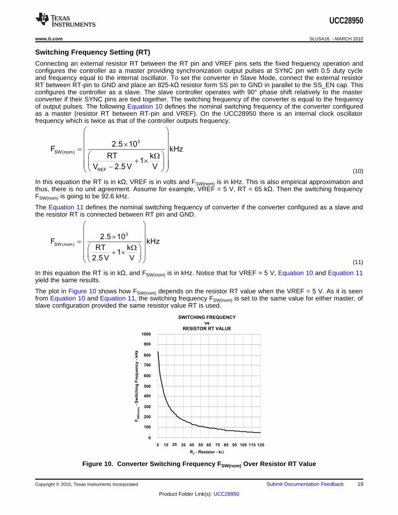
Switching Frequency Setting (RT)
Connecting an external resistor RT between the RT pin and VREF pins sets the fixed frequency operation andconfigures the controller as a master providing synchronization output pulses at SYNC pin with 0.5 duty cycleand frequency equal to the internal oscillator. To set the converter in Slave Mode, connect the external resistorRT between RT-pin to GND and place an 825-kΩ resistor form SS pin to GND in parallel to the SS_EN cap. Thisconfigures the controller as a slave. The slave controller operates with 90° phase shift relatively to the masterconverter if their SYNC pins are tied together. The switching frequency of the converter is equal to the frequencyof output pulses. The following Equation 10 defines the nominal switching frequency of the converter configuredas a master (resistor RT between RT-pin and VREF). On the UCC28950 there is an internal clock oscillatorfrequency which is twice as that of the controller outputs frequency.
(10)
In this equation the RT is in kΩ, VREF is in volts and FSW(nom) is in kHz. This is also empirical approximation andthus, there is no unit agreement. Assume for example, VREF = 5 V, RT = 65 kΩ. Then the switching frequencyFSW(nom) is going to be 92.6 kHz.
The Equation 11 defines the nominal switching frequency of converter if the converter configured as a slave andthe resistor RT is connected between RT pin and GND.
(11)
In this equation the RT is in kΩ, and FSW(nom) is in kHz. Notice that for VREF = 5 V, Equation 10 and Equation 11yield the same results.
The plot in Figure 10 shows how FSW(nom) depends on the resistor RT value when the VREF = 5 V. As it is seenfrom Equation 10 and Equation 11, the switching frequency FSW(nom) is set to the same value for either master, ofslave configuration provided the same resistor value RT is used.
Figure 10. Converter Switching Frequency FSW(nom) Over Resistor RT Value
Copyright © 2010, Texas Instruments Incorporated Submit Documentation Feedback 19
Product Folder Link(s): UCC28950

Oscillator
Ramp
Generator
Ramp
Summing
Two Direction
Current Sense11
15
4COMP
CS
RSUM
+
+
2 V
7
GND
CLK
RAMP
VMC
PCM
Cycle-by-Cycle ILIM
Mode Select
CS_SLOPECOMP
VREF VCM
GND PCM
+
0.85 V
-+
SUM
2.5 Vme
0.5 R s
æ ö= ç ÷
´ mè ø
UCC28950
SLUSA16 –MARCH 2010 www.ti.com
Slope Compensation (RSUM)
Slope compensation is the technique that adds additional ramp signal to the CS signal and applied to the:• Input of PWM comparator in case of peak current mode control.• Input of cycle-by-cycle current limit comparator.
This prevents sub-harmonic oscillation at D > 50% (some publications suggest it might happen even at D <50%). At low duty cycle and light load, the slope compensation ramp reduces noise sensitivity of Peak CurrentMode control.
Too much additional slope compensation ramp reduces benefits of PCM control. In case of cycle-by-cyclecurrent limit, the average current limit becomes lower and this might reduce the start up capability with the largeoutput capacitance. The optimal compensation slope varies depending on duty cycle, LO and LM.
The slope compensation is needed for the controller operating at peak current mode control or during thecycle-by-cycle current limit at duty cycle above 50%. Placing a resistor from RSUM pin to ground allows thecontroller to operate in peak current control mode. Connecting RSUM pin through resistor to VREF switchescontroller to the voltage mode control with the internal PWM ramp. However, the resistor value still provides CSsignal compensation for cycle-by-cycle current limit. In other words, in VMC, the slope compensation is appliedonly to cycle-by-cycle comparator. While in PCM, the slope compensation applied to both PWM andcycle-by-cycle current limit comparators.
The operation logic of slope compensation circuit is shown in Figure 11.
Figure 11. The Operation Logic of Slope Compensation Circuit
The slope of the additional ramp, me, added to CS signal by placing a resistor from RSUM pin to the ground isdefined by the following Equation 12.
(12)
20 Submit Documentation Feedback Copyright © 2010, Texas Instruments Incorporated
Product Folder Link(s): UCC28950

REF
SUM
(V 2.5 V) Vme
0.5 R s
æ ö-= ç ÷
´ mè ø
5 200
Rsum
- Resistor - kW
0.50
100
Slo
pe
-V
/ms
SLOPE
vs
RESISTOR
0.45
0.10
0
0.30
0.20
0.05
0.25
20 40 80 120 140 18060 160
0.15
0.40
0.35
UCC28950
www.ti.com SLUSA16 –MARCH 2010
If the resistor from RSUM pin is connected to VREF pin, then the controller operates in voltage mode control, stillhaving the slope compensation added to CS signal used for cycle-by-cycle current limit. In such a case the slopeis defined by the following Equation 13.
(13)
In Equation 12 and Equation 13, the VREF is in volts, RSUM is in kΩ, and me is in V/µs. These are empiricalequations without unit agreement. As an example, substituting VREF = 5 V and RSUM = 40 kΩ, yields the result0.125 V/µs. The related plot of me as function of RSUM is shown in Figure 12. Because VREF = 5 V, the plotsgenerated from Equation 12 and Equation 13 coincide.
Figure 12. Slope of the Added Ramp Over Resistor RSUM
Copyright © 2010, Texas Instruments Incorporated Submit Documentation Feedback 21
Product Folder Link(s): UCC28950
RDCM(hi)
RDCM
1
15
12
VREF
CS
DCM
20 mA
R = 77 kW
C = 6.5 pF
R = 77 kW
C = 6.5 pF
+
DCM_COMP2-Cycle
Counter
0 = DCM
1 = CCM
PWM
Moving into
DCM Mode
0 10
Load Current - A
0.8
4
Du
tyC
yc
le-
%
DUTY CYCLE
vs
LOAD CURRENT
0.4
0
0.6
0.2
1 2 3 5 6 7 8 9
VS(min)
VS(max)
Burst Mode
Area
Setting DMIN
15.6%
UCC28950
SLUSA16 –MARCH 2010 www.ti.com
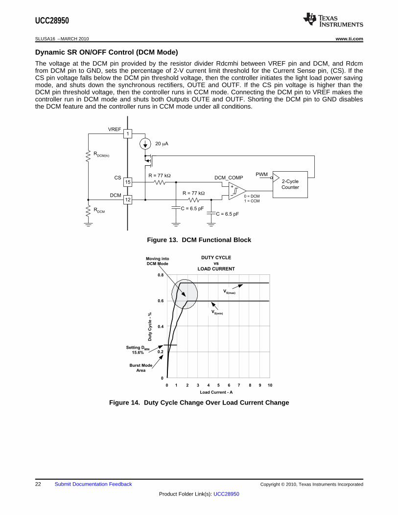
Dynamic SR ON/OFF Control (DCM Mode)
The voltage at the DCM pin provided by the resistor divider Rdcmhi between VREF pin and DCM, and Rdcmfrom DCM pin to GND, sets the percentage of 2-V current limit threshold for the Current Sense pin, (CS). If theCS pin voltage falls below the DCM pin threshold voltage, then the controller initiates the light load power savingmode, and shuts down the synchronous rectifiers, OUTE and OUTF. If the CS pin voltage is higher than theDCM pin threshold voltage, then the controller runs in CCM mode. Connecting the DCM pin to VREF makes thecontroller run in DCM mode and shuts both Outputs OUTE and OUTF. Shorting the DCM pin to GND disablesthe DCM feature and the controller runs in CCM mode under all conditions.
Figure 13. DCM Functional Block
Figure 14. Duty Cycle Change Over Load Current Change
22 Submit Documentation Feedback Copyright © 2010, Texas Instruments Incorporated
Product Folder Link(s): UCC28950

5 DCMHI DCM
DCMHI DCM
R RV 2 10
R R
- ´D = ´
+
PWM
DCM Threshold
+ Hysteresis
CS
E
F
PWM
DCM Threshold
+ Hysteresis
CS
E
F
UCC28950
www.ti.com SLUSA16 –MARCH 2010
There is a nominal 20-µA switched current source used to create hysteresis. The current source is active onlywhen the system is in DCM Mode. Otherwise, it is inactive and does not affect the node voltage. Therefore, whenbeing in DCM region, the DCM threshold is the voltage divider plus ΔV explained in Equation 14 below. Whenbeing in CCM region, the threshold is the voltage set by the resistor divider. When CS pin reaches the thresholdset on the DCM pin, the system waits to see two consecutive falling edge PWM cycles before switching fromCCM to DCM and vice-versa. The magnitude of the hysteresis is a function of the external resistor dividerimpedance. The hysteresis can be calculated using the following Equation 14:
(14)
Figure 15. Moving from DCM to CCM Mode
Figure 16. Moving from CCM to DCM Mode
DCM must be used in order to prevent reverse current in the output inductor which could cause the synchronousFETS to fail.
Copyright © 2010, Texas Instruments Incorporated Submit Documentation Feedback 23
Product Folder Link(s): UCC28950

( )( )DS(master )I 25 1 D 5 A= - ´ - + m
( )( )DS(slave)I 25 1 D A= - ´ - m
.
Soft Restart
OFF Time Before Restart
Cycle-by-Cycle ILIM
Normal
OperationSoft Start
IHCC
= 2.5 mA
IDS
= (-25 x (1-D)+5) mA
25 mA
Fast Pull Up
by 1 kW Switch
ISS
=25 mA
4.65
3.703.60
0.55
0.00
SS Pin (V)
SS Clamp Voltage
Pull Up Threshold
Output Enable
Threshold
Output Pulses (D)
UCC28950
SLUSA16 –MARCH 2010 www.ti.com
Current Sensing (CS)
The signal from current sense pin is used for cycle-by-cycle current limit, peak-current mode control, light-loadefficiency management and setting the delay time for outputs OUTA, OUTB, OUTC, OUTD and delay time foroutputs OUTE, OUTF. Connect the current sense resistor RCS between CS and GND. Depending on layout, toprevent a potential electrical noise interference, it is recommended to put a small R-C filter between RCS resistorand CS pin.
Cycle-by-Cycle Current Limit Current Protection and Hiccup Mode
The cycle-by-cycle current limit provides peak current limiting on the primary side of the converter when the loadcurrent exceeds its predetermined threshold. For peak current mode control, certain leading edge blanking timeis needed to prevent the controller from false tripping due to switching noise. In order to save external RC filterfor the blanking time, an internal 30-ns filter at CS input is provided. The total propagation delay TCS from CSpin to outputs is 100 ns. An external RC filter is still needed if the power stage requires more blanking time. The2.0-V ±3% cycle-by-cycle current limit threshold is optimized for efficient current transformer based sensing. Theduration when a converter operates at cycle-by-cycle current limit depends on the value of soft-start capacitorand how severe the over current condition is. This is achieved by the internal discharge current IDS Equation 15and Equation 16 at SS pin.
(15)
(16)
The soft-start capacitor value also determines the so called hiccup mode off-time duration. The behavior of theconverter during different modes of operation, along with related soft start capacitor charge/discharge currentsare shown in Figure 17.
Figure 17. Timing Diagram of Soft-Start Voltage VSS
24 Submit Documentation Feedback Copyright © 2010, Texas Instruments Incorporated
Product Folder Link(s): UCC28950

( )SS
CL(on _ master )
C 4.65 V 3.7 VT
20 A
´ -=
m
( )SS
CL(on _ slave)
C 4.65 V 3.7 VT
25 A
´ -=
m
( )SS
CL(off _ master )
C 3.6 V 0.55 VT
2.5 A
´ -=
m
( )SS
CL(off _ slave)
C 3.6 V 0.55 VT
4.9 A
´ -=
m
UCC28950
www.ti.com SLUSA16 –MARCH 2010
The largest discharge current of 20 µA is when the duty cycle is close to zero. This current sets the shortestoperation time during the cycle-by-cycle current limit which is defined as:
(17)
(18)
Thus, if the soft-start capacitor CSS = 100 nF is selected, then the TCL(on) time will be 5 ms.
To calculate the hiccup off time TCL(off) before the restart, the following Equation 19 or Equation 20 needs to beused:
(19)
(20)
With the same soft start capacitor value 100 nF, the off time before the restart is going to be 122 ms. Notice, thatif the over current condition happens before the soft start capacitor voltage reaches the 3.7-V threshold duringstart up, the controller limits the current but the soft start capacitor continues to be charged. As soon as the 3.7-Vthreshold is reached, the soft-start voltage is quickly pulled up to the 4.65-V threshold by an internal 1-kΩ RDS(on)switch and the cycle-by-cycle current limit duration timing starts by discharging the soft start capacitor.Depending on specific design requirements, the user can override default parameters by applying externalcharge or discharge currents to the soft start capacitor. The whole cycle-by-cycle current limit and hiccupoperation is shown in Figure 17. In this example the cycle-by-cycle current limit lasts about 5 ms followed by 122ms of off time.
Similar to the over current condition, the hiccup mode with the restart can be overridden by the user if a pull upresistor is connected between the SS and VREF pins. If the pull up current provided by the resistor exceeds 2.5µA, then the controller remains in the latch off mode. In this case, an external soft-start capacitor value should becalculated with the additional pull-up current taken into account. The latch off mode can be reset externally if thesoft-start capacitor is forcibly discharged below 0.55 V or the VDD voltage is lowered below the UVLO threshold.
Copyright © 2010, Texas Instruments Incorporated Submit Documentation Feedback 25
Product Folder Link(s): UCC28950

CLK
SYNC_OUT
A
B
CLK
SYNC_IN
A
B
UCC28950
SLUSA16 –MARCH 2010 www.ti.com
Synchronization (SYNC)
The UCC28950 allows flexible configuration of converters operating in synchronized mode by connecting allSYNC pins together and by configuration of the controllers as master and/or slaves. The controller configured asMaster (resistor between RT and VREF) provides synchronization pulses at the SYNC pin with the frequencyequal to 2X the converter frequency FSW(nom) and 0.5 duty cycle. The controller configured as a Slave (resistorbetween RT and GND and 825-kΩ resistor between SS_EN pin to GND) does not generate the synchronizationpulses. The Slave controller synchronizes its own clock to the falling edge of synchronization signal thusoperating 90° phase shifted versus the master converter’s frequency FSW(nom). Because the Slave issynchronized to the falling edge of the SYNC pulses, the slave operates at 180˚ delayed versus Master’s CLK or90˚ delayed versus output switching pulses of Master.
Such operation between Master and Slave provides maximum input capacitor and output capacitor ripplecancellation effect if inputs and outputs of converters are tied together. To avoid system issues during thesynchronized operation of few converters the following conditions should be taken care of.• If any converter is configured a as a Slave, the SYNC frequency must be greater than or equal to 1.8 times
the converter frequency.• Slave converter does not start until at least one synchronization pulse has been received.• If any or all converters are configured as Slaves, then each converter operates at its own frequency without
synchronization after receiving at least one synchronization pulse. Thus, If there is an interruption ofsynchronization pulses at the slave converter, then the controller uses its own internal clock pulses tomaintain operation based on the RT value that is connected to GND in the Slave converter.
• In Master mode, SYNC pulses start after SS pin passes its Enable threshold which is 0.55 V.• Slave starts generating SS/EN voltage even though synchronization pulses have not been received.• It is recommended that the SS on the Master controller starts before the SS on the Slave controller; therefore
SS/EN pin on master converter must reach its Enable threshold voltage before SS/EN on the slave converterstarts for proper operation. On the same note, it’s recommended that TMIN resistors on both Master and Slaveare set at the same value.
Figure 18. SYNC_OUT (Master Mode) Timing Diagram
Figure 19. SYNC_IN (Slave Mode) Timing Diagram
26 Submit Documentation Feedback Copyright © 2010, Texas Instruments Incorporated
Product Folder Link(s): UCC28950

RPR
Lm
XT
LLK
COSS
COSS
A
OUTA
OUTB
+
-
COSS
COSS
B
OUTC
OUTD
1T 1T
COSS C
OSS
OUTE OUTF
CO
VOUT- +
LO
DCR
UCC28950
www.ti.com SLUSA16 –MARCH 2010
Outputs (OUTA, OUTB, OUTC, OUTD, OUTE, OUTF)• All MOSFET control outputs have 0.2-A drive capability.• The control outputs are configured as P-MOS and N-MOS totem poles with typical RDS(on) 20 Ω and 10 Ω
accordingly.• The control outputs are capable of charging 100-pF capacitor within 12 ns and discharge within 8 ns.• The amplitude of output control pulses is equal to VDD.• Control outputs are designed to be used with external gate MOSFET/IGBT drivers.• The design is optimized to prevent the latch up of outputs and verified by extensive tests.
The UCC28950 has outputs OUTA, OUTB driving the active leg, initiating the duty cycle leg of power MOSFETsin phase-shifted full bridge power stage, and outputs OUTC, OUTD driving the passive leg, completing the dutycycle leg, as it is shown in typical timing diagram in Figure 47. Outputs OUTE and OUTF are optimized to drivethe synchronous rectifier MOSFETs (Figure 20). These outputs have 200-mA peak-current capabilities and aredesigned to drive relatively small capacitive loads like inputs of external MOSFET or IGBT drivers.Recommended load capacitance should not exceed 100 pF. The amplitude of output signal is equal to VDDvoltage.
Figure 20. Power Stage
Copyright © 2010, Texas Instruments Incorporated Submit Documentation Feedback 27
Product Folder Link(s): UCC28950
1
2
3
4
5
6
7
8
9
10
11
12
UCC28950
DCM
RSUM
RT
TMIN
DELEF
DELCD
DELAB
SS/EN
COMP
EA-
EA+
VREF 24
23
22
21
20
19
18
17
16
15
14
13ADELEF
ADEL
CS
SYNC
OUTF
OUTE
OUTD
OUTC
OUTB
OUTA
VDD
GND
RDCM
RCS
R7
RA(hi)
A
B
C
D
E
F
VDD
SYNC
VREF
R5
C2
C1
R4
R3
CREF
R2R1
VSENSE
ENABLE
Current Sense
Analog
Plane
Power
Plane
RAEF(hi)
RA
RAEF
RDCM(hi)
CSS
RAB
RCD
REF
RT(min)
RT
RSUM)
CVDD
C3R6
UCC28950
SLUSA16 –MARCH 2010 www.ti.com
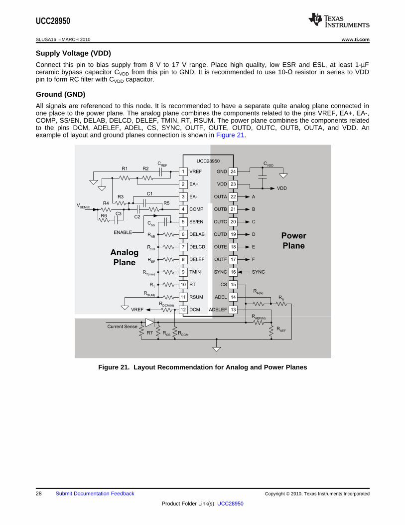
Supply Voltage (VDD)
Connect this pin to bias supply from 8 V to 17 V range. Place high quality, low ESR and ESL, at least 1-µFceramic bypass capacitor CVDD from this pin to GND. It is recommended to use 10-Ω resistor in series to VDDpin to form RC filter with CVDD capacitor.
Ground (GND)
All signals are referenced to this node. It is recommended to have a separate quite analog plane connected inone place to the power plane. The analog plane combines the components related to the pins VREF, EA+, EA-,COMP, SS/EN, DELAB, DELCD, DELEF, TMIN, RT, RSUM. The power plane combines the components relatedto the pins DCM, ADELEF, ADEL, CS, SYNC, OUTF, OUTE, OUTD, OUTC, OUTB, OUTA, and VDD. Anexample of layout and ground planes connection is shown in Figure 21.
Figure 21. Layout Recommendation for Analog and Power Planes
28 Submit Documentation Feedback Copyright © 2010, Texas Instruments Incorporated
Product Folder Link(s): UCC28950

-40 125
TJ
- Temperature - °C
6.2
6.4
6.8
7.0
7.6
25
6.6
7.2
7.4
UV
LO
-U
nd
er
Vo
lta
ge
Lo
ck
ou
tT
hre
sh
old
s-
V
UVLO THRESHOLDS
vs
TEMPERATURE
UVLO_RTH
UVLO_FTH
-40 125
TJ
- Temperature - °C
580
590
610
640
25
600
620
630
UV
LO
-U
nd
er
Vo
lta
ge
Lo
ck
ou
tH
ys
tere
sis
-m
V
UVLO HYSTERESIS
vs
TEMPERATURE
UVLO_HYST
-40 125
TJ
- Temperature - °C
3.4
3.5
3.6
3.9
25
3.7
3.8
I DD
-O
pe
rati
ng
Su
pp
lyC
urr
en
t-
mA
SUPPLY CURRENT
vs
TEMPERATURE
-40 125
TJ
- Temperature - °C
50
100
150
250
25
200
I DD
-S
tart
up
Cu
rre
nt
-m
A
STARTUP CURRENT
vs
TEMPERATURE
UCC28950
www.ti.com SLUSA16 –MARCH 2010
TYPICAL CHARACTERISTICS
Figure 22. Figure 23.
Figure 24. Figure 25.
Copyright © 2010, Texas Instruments Incorporated Submit Documentation Feedback 29
Product Folder Link(s): UCC28950

-40 125
TJ
- Temperature - °C
5.010
25
VR
EF
-V
olt
ag
eR
efe
ren
ce
-V
VOLTAGE REFERENCE (VDD = 12 V)
vs
TEMPERATURE
5.005
4.995
4.985
4.975
5.000
4.990
4.980
ILOAD
= 10 mA
ILOAD
= 1 mA
ILOAD
= 10 mA
ILOAD
= 20 mA
-40 125
TJ
- Temperature - °C
5.001
25
VR
EF
-L
ine
Vo
lta
ge
Re
gu
lati
on
-V
LINE VOLTAGE REGULATION (ILOAD
= 10 mA)
vs
TEMPERATURE
4.999
4.995
4.991
4.987
4.997
4.993
4.989
4.985
VREF
_ 10 mA _ 12 VDD
VREF
_ 10 mA _ 10 VDD
VREF
_ 10 mA _ 8 VDD
-40 125
TJ
- Temperature - °C
35.0
36.0
36.5
38.5
25
38.0
Sh
ort
Cir
cu
itC
urr
en
t-
mA
SHORT CIRCUIT CURRENT
vs
TEMPERATURE
37.5
37.0
35.5
-40 125
TJ
- Temperature - °C
93.6
94.2
94.4
95.4
25
95.2
DM
AX
-M
ax
imu
mD
uty
Cy
cle
-%
MAXIMUM DUTY CYCLE
vs
TEMPERATURE
95.0
94.6
93.8
94.8
94.0
UCC28950
SLUSA16 –MARCH 2010 www.ti.com
TYPICAL CHARACTERISTICS (continued)
Figure 26. Figure 27.
Figure 28. Figure 29.
30 Submit Documentation Feedback Copyright © 2010, Texas Instruments Incorporated
Product Folder Link(s): UCC28950
-40 125
TJ
- Temperature - °C
999
1079
25
FS
W(m
ax
)-
Ma
xim
um
Sw
itc
hin
gF
req
ue
nc
y-
Hz
MAXIMUM SWITCHING FREQUENCY
vs
TEMPERATURE
1059
1039
1019
-40 125
TJ
- Temperature - °C
93.6
95.4
25
FS
W(n
om
)-
No
min
al
Sw
itc
hin
gF
req
ue
nc
y-
Hz
NOMINAL SWITCHING FREQUENCY
vs
TEMPERATURE
95.0
94.6
94.0
-40 125
TJ
- Temperature - °C
-0.50
0.00
25
Err
or
Am
pli
fie
rO
FF
SE
Tv
olt
ag
e-
mV
ERROR AMPLIFIER OFFSET VOLTAGE
vs
TEMPERATURE
-0.05
-0.15
-0.25
-0.45
-0.35
VIO
= 500 mV
VIO
= 3.6 V
VIO
= 2.5 V
-0.10
-0.20
-0.30
-0.40
-40 125
TJ
- Temperature - °C
85
125
25
AV
OL
-V
olt
ag
eE
rro
rA
mp
lifi
er
-d
B
VOLTAGE ERROR AMPLIFIER
(Open Loop Gain)
vs
TEMPERATURE
115
105
95
120
110
100
90
UCC28950
www.ti.com SLUSA16 –MARCH 2010
TYPICAL CHARACTERISTICS (continued)
Figure 30. Figure 31.
Figure 32. Figure 33.
Copyright © 2010, Texas Instruments Incorporated Submit Documentation Feedback 31
Product Folder Link(s): UCC28950

-40 125
TJ
- Temperature - °C
23.5
26.0
25
I SS
-C
ha
rge
Cu
rre
nt
-m
A
ISS
CHARGE CURRENT
vs
TEMPERATURE
25.5
25.0
24.5
24.0
-40 125
TJ
- Temperature - °C
0.30
0.60
25
VS
S(s
td)-
Sh
utd
ow
n/R
es
tart
/Re
se
tT
hre
sh
old
-V
SHUTDOWN/RESTART/RESET THRESHOLD
vs
TEMPERATURE
0.45
0.40
0.55
0.50
0.35
-40 125
TJ
- Temperature - °C
3.69
3.71
25
VS
S(p
u)-
SS
Pu
llu
pT
hre
sh
old
-V
SS PULL-UP THRESHOLD
vs
TEMPERATURE
3.70
3.70
3.71
-40 125
TJ
- Temperature - °C
4.67
4.69
25
VS
S(C
L)-
SS
Cla
mp
Vo
lta
ge
-V
SS CLAMP VOLTAGE
vs
TEMPERATURE
4.68
4.68
4.68
4.68
4.67
4.69
4.68
4.67
UCC28950
SLUSA16 –MARCH 2010 www.ti.com
TYPICAL CHARACTERISTICS (continued)
Figure 34. Figure 35.
Figure 36. Figure 37.
32 Submit Documentation Feedback Copyright © 2010, Texas Instruments Incorporated
Product Folder Link(s): UCC28950

-40 125
TJ
- Temperature - °C
1.984
1.996
25
VC
S(l
im)-
Cu
rre
nt
Se
ns
eC
yc
le-B
y-C
yc
leL
imit
-V
CURRENT SENSE CYCLE-BY-CYCLE LIMIT
vs
TEMPERATURE
1.990
1.988
1.994
1.992
1.986
-40 125
TJ
- Temperature - °C
95
110
25
TC
S(p
rop
)-
Cu
rre
nt
Se
ns
eP
rop
ag
ati
on
De
lay
-n
s
CURRENT SENSE PROPAGATION DELAY
vs
TEMPERATURE
107
104
101
98
-40 125
TJ
- Temperature - °C
25
RS
INK
-O
utp
uts
Sin
kR
es
ista
nc
e-
W
OUTPUTS SINK RESISTANCE
vs
TEMPERATURE
17.5
13.5
11.5
7.5
15.5
9.5
RSINK_OUTB
RSINK_OUTC
RSINK_OUTE
-40 125
TJ
- Temperature - °C
25
RS
INK
-O
utp
uts
Sin
kR
es
ista
nc
e-
W
OUTPUTS SINK RESISTANCE
vs
TEMPERATURE
17.5
13.5
11.5
7.5
15.5
9.5
RSINK_OUTA
RSINK_OUTD
RSINK_OUTF
UCC28950
www.ti.com SLUSA16 –MARCH 2010
TYPICAL CHARACTERISTICS (continued)
Figure 38. Figure 39.
Figure 40. Figure 41.
Copyright © 2010, Texas Instruments Incorporated Submit Documentation Feedback 33
Product Folder Link(s): UCC28950

-40 125
TJ
- Temperature - °C
25
RS
RC
-O
utp
uts
So
urc
eR
es
ista
nc
e-
W
OUTPUTS SOURCE RESISTANCE
vs
TEMPERATURE
25
21
19
15
23
17
RSRC_OUTA
RSRC_OUTC
RSRC_OUTF
-40 125
TJ
- Temperature - °C
25
RS
RC
-O
utp
uts
So
urc
eR
es
ista
nc
e-
W
OUTPUTS SOURCE RESISTANCE
vs
TEMPERATURE
25
21
19
15
23
17
RSRC_OUTB
RSRC_OUTD
RSRC_OUTE
-40 125
TJ
- Temperature - °C
30
50
25
TO
FF
TIM
E-
De
ad
Tim
eD
ela
y-
ns
DEAD TIME DELAY
vs
TEMPERATURE
45
40
35
TCDSET2
TABSET2
TAFSET2
TBESET2
-40 125
TJ
- Temperature - °C
220
280
25
TO
FF
TIM
E-
De
ad
Tim
eD
ela
y-
ns
DEAD TIME DELAY
vs
TEMPERATURE
270
260
250
230
240
TCDSET2
TABSET2
TAFSET2
TBESET2
UCC28950
SLUSA16 –MARCH 2010 www.ti.com
TYPICAL CHARACTERISTICS (continued)
Figure 42. Figure 43.
Figure 44. Figure 45.
34 Submit Documentation Feedback Copyright © 2010, Texas Instruments Incorporated
Product Folder Link(s): UCC28950

-40 125
TJ
- Temperature - °C
0.375
0.405
25
DC
M-
DC
MT
hre
sh
old
-V
DCM THRESHOLD
vs
TEMPERATURE
0.400
0.390
0.385
0.380
0.395
0.380
UCC28950
www.ti.com SLUSA16 –MARCH 2010
TYPICAL CHARACTERISTICS (continued)
Figure 46.
Copyright © 2010, Texas Instruments Incorporated Submit Documentation Feedback 35
Product Folder Link(s): UCC28950

IOUT
VOUT
x (1-D) / D
VOUT
TON
= 0.5 x D x TSW(nom)
ILOUT
VLOUT
VDS
QF
VDS
QE
IPR
TAFSET2
TAFSET1
TBESET1
TBESET2
TABSET1
TCDSET2
TABSET2
TSW(nom)
TSW(osc)
OUTE
OUTF
OUTD
OUTC
OUTB
OUTA
TCDSET1
UCC28950
SLUSA16 –MARCH 2010 www.ti.com
APPLICATION INFORMATION
UCC28950 Application Description
The efficiency improvement of phase-shifted full-bridge DC/DC converter with UCC28950 is achieved by usingthe synchronous rectification technique, control algorithm providing ZVS condition over the entire load currentrange, accurate adaptive timing of the control signals between primary and secondary FETs and specialoperating modes at light load for the highest efficiency and power saving. The simplified electrical diagram of thisconverter is shown in Figure 47. The controller device is located on the secondary side of converter, although itcould be located on primary side as well. The location on secondary side allows easy power system levelcommunication and better handling of some transient conditions that require fast direct control of thesynchronous rectifier MOSFETs. The power stage includes primary side MOSFETs, QA, QB, QC, QD andsecondary side synchronous rectifier MOSFETs, QE and QF. For example, for the 12-V output converters inserver power supplies use of the center-tapped rectifier scheme with L-C output filter is a popular choice.
To maintain high efficiency at different output power conditions, the converter operates in nominal synchronousrectification mode at mid and high output power levels, with transitioning to the diode rectifier mode at light loadand further followed by the burst mode, as the output power becomes even lower. All these transitions are basedon the current sensing on the primary side using the current sense transformer in this specific case.
Figure 47. Major Waveforms of Phase-Shifted Converter
36 Submit Documentation Feedback Copyright © 2010, Texas Instruments Incorporated
Product Folder Link(s): UCC28950

OUTE
(CCM Mode)
OUTF
(CCM Mode)
OUTE
OUTF
Transformer
Winding
Magnetizing
Current
OUTE and OUTF are disabled if VCS
< VDCM
OUTE and OUTF are disabled if VCS
< VDCM
Burst Mode at light load with TMIN
maintaining ZVS
(The time scale is different versus above diagram)
UCC28950
www.ti.com SLUSA16 –MARCH 2010
Major waveforms of the phase-shifted converter during nominal operation mode are shown in Figure 47. Uppersix waveforms in the Figure 47 show the output drive signals of the controller. At nominal mode, the outputsOUTE and OUTF overlap during the part of the switching cycle when the both rectifier MOSFETs are conductingand the windings of power transformer are shorted. Current, IPR, is the current flowing through the primarywinding of power transformer. The bottom four waveforms show the drain-source voltages of rectifier MOSFETs,VDS_QE and VDS_QF, the voltage at the output inductor, V LOUT, and the current through the output inductor, I LOUT.Proper timing between the primary switches and synchronous rectifier MOSFETs is critical to achieve highestefficiency and reliable operation in this mode. The controller device adjusts the turn OFF timing of rectifierMOSFETs as function of load current to ensure the minimum conduction time and reverse recovery losses oftheir internal body diodes.
ZVS is an important feature of relatively high input voltage converters to reduce switching losses associated withthe internal parasitic capacitances of power switches and transformers. The controller ensures ZVS conditionsover the entire load current range by adjusting the delay time between the primary MOSFETs switching in thesame leg in accordance to the load variation. Controller also limits the minimum ON-time pulse applied to thepower transformer at light load, allowing the storage of sufficient energy in the inductive components of powerstage for the ZVS transition.
As soon as the load current keeps reducing from the mid load current down to no-load condition, the controllerselects the most efficient power saving mode by moving the converter from the nominal operation mode to thediscontinuous-current diode-rectification mode and, eventually, at very light-load and at no-load condition, to theburst mode. These modes and related output signals, OUTE, OUTF, driving the rectifier MOSFETs, are shown inFigure 48.
Figure 48. Major Waveforms During Transitions Between Different Operating Modes
Copyright © 2010, Texas Instruments Incorporated Submit Documentation Feedback 37
Product Folder Link(s): UCC28950
1 kW
+
RZ1
CZ1
CZ1
EA-
EA+
RI
R
VREF
R
RI
CZ2
RZ2
VOUT
When evaluating COMP, for best
results put a 1-kW resistor between
COMP and probe.
UCC28950
SLUSA16 –MARCH 2010 www.ti.com
It is necessary to prevent the reverse current flow through the synchronous rectifier MOSFETs and outputinductor at the light load, during parallel operation and at some transient conditions. Such reverse current resultsin circulating of some extra energy between the input voltage source and the load and, therefore, causesincreased losses and reduces efficiency. Another negative effect of such reverse current is the loss of ZVScondition. The suggested control algorithm prevents reverse current flow, still maintaining most of the benefits ofsynchronous rectification by switching off the drive signals of rectifier MOSFETs in a predetermined way. Atsome pre-determined load current threshold, the controller disables outputs OUTE and OUTF by bringing themdown to zero.
Synchronous rectification using MOSFETs requires some electrical energy to drive the MOSFETs. There is acondition below some light-load threshold when the MOSFET drive related losses exceed the saving provided bythe synchronous rectification. At such light load, it is best to disable the drive circuit and use the internal bodydiodes of rectifier MOSFETs, or external diodes in parallel with the MOSFETs, for more efficient rectification. Inmost practical cases, the drive circuit needs to be disabled close to DCM mode. This mode of operation is calleddiscontinuous-current diode-rectification mode.
At very light-load and no-load condition, the duty cycle, demanded by the closed-feedback-loop control circuit foroutput voltage regulation, can be very low. This could lead to the loss of ZVS condition and increased switchinglosses. To avoid the loss of ZVS, the control circuit limits the minimum ON-time pulse applied to the powertransformer using resistor from TMIN pin to GND. Therefore, the only way to maintain regulation at very light loadand at no-load condition is to skip some pulses. The controller skips pulses in a controllable manner to avoidsaturation of the power transformer. Such operation is called burst mode. In Burst Mode there are always aneven number of pulses applied to the power transformer before the skipping off time. Thus, the flux in the core ofthe power transformer always starts from the same point during the start of every burst of pulses.
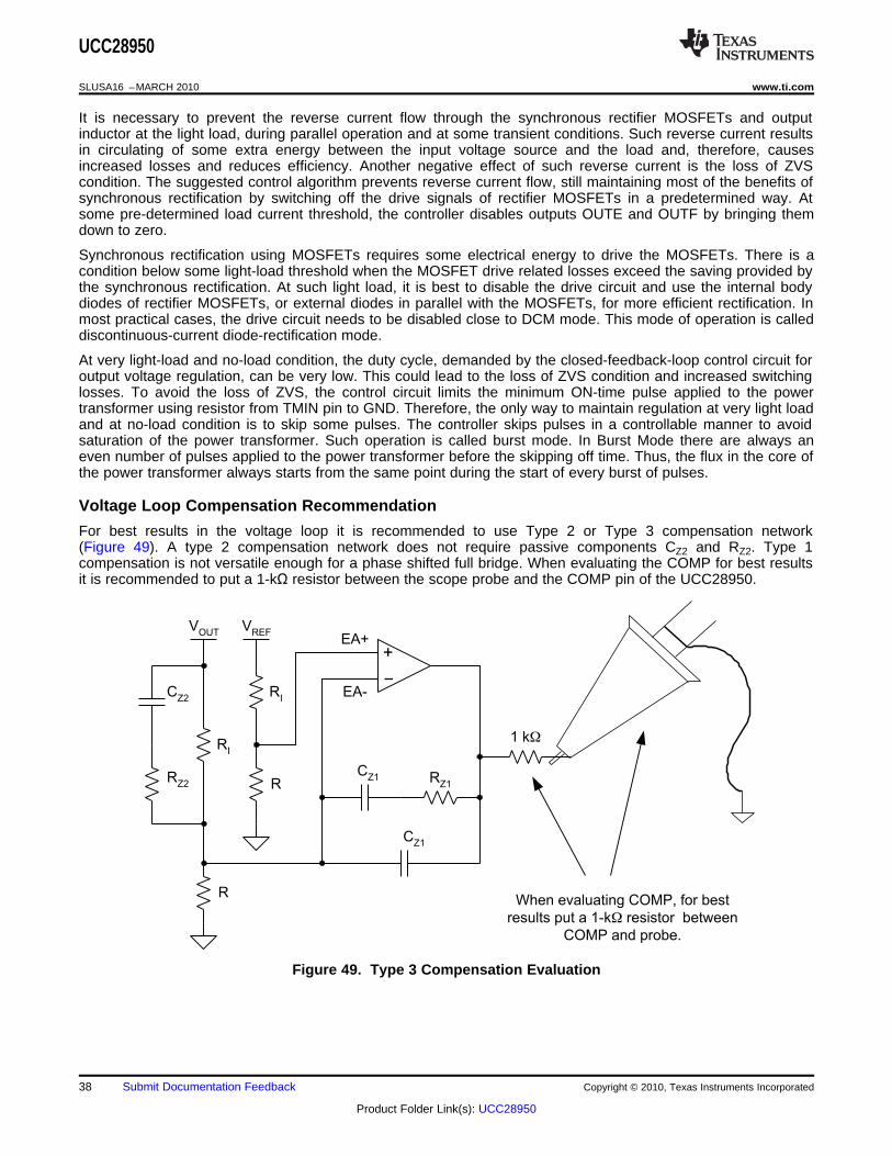
Voltage Loop Compensation Recommendation
For best results in the voltage loop it is recommended to use Type 2 or Type 3 compensation network(Figure 49). A type 2 compensation network does not require passive components CZ2 and RZ2. Type 1compensation is not versatile enough for a phase shifted full bridge. When evaluating the COMP for best resultsit is recommended to put a 1-kΩ resistor between the scope probe and the COMP pin of the UCC28950.
Figure 49. Type 3 Compensation Evaluation
38 Submit Documentation Feedback Copyright © 2010, Texas Instruments Incorporated
Product Folder Link(s): UCC28950

0 55
Load Current - A
100
25
Eff
icie
nc
y-
%
EFFICIENCY
vs
LOAD CURRENT
98
90
86
80
94
88
82
96
92
84
5 10 15 20 30 35 40 45 50
VIN
= 400 V with LRES
VIN
= 350 V with LRES
VIN
= 300 V with LRES
0 2.0
Load Current - A
12
0.8
Lig
ht-
Lo
ad
Po
we
rL
os
se
s-
W
LIGHT-LOAD POWER LOSSES
vs
LOAD CURRENT
11
6
4
0
9
5
2
10
7
3
0.2 0.4 0.6 1.0 1.2 1.4 1.6 1.8
8
1
Burst Mode
DCM Mode
with Diode
Rectification
CCM Mode with
Synchronous FETs
UCC28950
www.ti.com SLUSA16 –MARCH 2010
Experimental Results Example
The following experimental results are based on 660-W output power prototype of phase shifted full-bridgeDC/DC converter. The input voltage is 300 V to 400 V and the output is 12 V, 55 A. The primary MOSFETs areSPA11N60CFD and the synchronous rectifier MOSFETs are FDP047AN08A0, two in parallel. The measuredefficiency of the prototype is shown in Figure 50.
Figure 50. Efficiency of the Prototype Phase-Shifted Converter(VIN = 300 V, 350 V and 400 V, VOUT = 12 V)
Because of the power saving need even at very light and no-load conditions, careful optimization of operation atlight load condition is required to set the proper boundaries between different operation modes. The result of thisoptimization is shown in Figure 51. This plot demonstrates the power savings while moving from the synchronousrectification mode above 1-A load current, into the discontinuous current mode with the diode rectificationbetween 0.3-A and 1-A load current, and eventually into the burst mode operation at load current below 0.3 A.
Figure 51. Power Losses of the Prototype at Light-Load and No-Load Conditions
Copyright © 2010, Texas Instruments Incorporated Submit Documentation Feedback 39
Product Folder Link(s): UCC28950

PACKAGING INFORMATION
Orderable Device Status (1) PackageType
PackageDrawing
Pins PackageQty
Eco Plan (2) Lead/Ball Finish MSL Peak Temp (3)
UCC28950PW ACTIVE TSSOP PW 24 60 Green (RoHS &no Sb/Br)
CU NIPDAU Level-1-260C-UNLIM
UCC28950PWR ACTIVE TSSOP PW 24 2000 Green (RoHS &no Sb/Br)
CU NIPDAU Level-1-260C-UNLIM
(1) The marketing status values are defined as follows:ACTIVE: Product device recommended for new designs.LIFEBUY: TI has announced that the device will be discontinued, and a lifetime-buy period is in effect.NRND: Not recommended for new designs. Device is in production to support existing customers, but TI does not recommend using this part ina new design.PREVIEW: Device has been announced but is not in production. Samples may or may not be available.OBSOLETE: TI has discontinued the production of the device.
(2) Eco Plan - The planned eco-friendly classification: Pb-Free (RoHS), Pb-Free (RoHS Exempt), or Green (RoHS & no Sb/Br) - please checkhttp://www.ti.com/productcontent for the latest availability information and additional product content details.TBD: The Pb-Free/Green conversion plan has not been defined.Pb-Free (RoHS): TI's terms "Lead-Free" or "Pb-Free" mean semiconductor products that are compatible with the current RoHS requirementsfor all 6 substances, including the requirement that lead not exceed 0.1% by weight in homogeneous materials. Where designed to be solderedat high temperatures, TI Pb-Free products are suitable for use in specified lead-free processes.Pb-Free (RoHS Exempt): This component has a RoHS exemption for either 1) lead-based flip-chip solder bumps used between the die andpackage, or 2) lead-based die adhesive used between the die and leadframe. The component is otherwise considered Pb-Free (RoHScompatible) as defined above.Green (RoHS & no Sb/Br): TI defines "Green" to mean Pb-Free (RoHS compatible), and free of Bromine (Br) and Antimony (Sb) based flameretardants (Br or Sb do not exceed 0.1% by weight in homogeneous material)
(3) MSL, Peak Temp. -- The Moisture Sensitivity Level rating according to the JEDEC industry standard classifications, and peak soldertemperature.
Important Information and Disclaimer:The information provided on this page represents TI's knowledge and belief as of the date that it isprovided. TI bases its knowledge and belief on information provided by third parties, and makes no representation or warranty as to theaccuracy of such information. Efforts are underway to better integrate information from third parties. TI has taken and continues to takereasonable steps to provide representative and accurate information but may not have conducted destructive testing or chemical analysis onincoming materials and chemicals. TI and TI suppliers consider certain information to be proprietary, and thus CAS numbers and other limitedinformation may not be available for release.
In no event shall TI's liability arising out of such information exceed the total purchase price of the TI part(s) at issue in this document sold by TIto Customer on an annual basis.
PACKAGE OPTION ADDENDUM
www.ti.com 15-Mar-2010
Addendum-Page 1

MECHANICAL DATA
MTSS001C – JANUARY 1995 – REVISED FEBRUARY 1999
POST OFFICE BOX 655303 • DALLAS, TEXAS 75265
PW (R-PDSO-G**) PLASTIC SMALL-OUTLINE PACKAGE14 PINS SHOWN
0,65 M0,10
0,10
0,25
0,500,75
0,15 NOM
Gage Plane
28
9,80
9,60
24
7,90
7,70
2016
6,60
6,40
4040064/F 01/97
0,30
6,606,20
8
0,19
4,304,50
7
0,15
14
A
1
1,20 MAX
14
5,10
4,90
8
3,10
2,90
A MAX
A MIN
DIMPINS **
0,05
4,90
5,10
Seating Plane
0°–8°
NOTES: A. All linear dimensions are in millimeters.B. This drawing is subject to change without notice.C. Body dimensions do not include mold flash or protrusion not to exceed 0,15.D. Falls within JEDEC MO-153

IMPORTANT NOTICE
Texas Instruments Incorporated and its subsidiaries (TI) reserve the right to make corrections, modifications, enhancements, improvements,and other changes to its products and services at any time and to discontinue any product or service without notice. Customers shouldobtain the latest relevant information before placing orders and should verify that such information is current and complete. All products aresold subject to TI’s terms and conditions of sale supplied at the time of order acknowledgment.
TI warrants performance of its hardware products to the specifications applicable at the time of sale in accordance with TI’s standardwarranty. Testing and other quality control techniques are used to the extent TI deems necessary to support this warranty. Except wheremandated by government requirements, testing of all parameters of each product is not necessarily performed.
TI assumes no liability for applications assistance or customer product design. Customers are responsible for their products andapplications using TI components. To minimize the risks associated with customer products and applications, customers should provideadequate design and operating safeguards.
TI does not warrant or represent that any license, either express or implied, is granted under any TI patent right, copyright, mask work right,or other TI intellectual property right relating to any combination, machine, or process in which TI products or services are used. Informationpublished by TI regarding third-party products or services does not constitute a license from TI to use such products or services or awarranty or endorsement thereof. Use of such information may require a license from a third party under the patents or other intellectualproperty of the third party, or a license from TI under the patents or other intellectual property of TI.
Reproduction of TI information in TI data books or data sheets is permissible only if reproduction is without alteration and is accompaniedby all associated warranties, conditions, limitations, and notices. Reproduction of this information with alteration is an unfair and deceptivebusiness practice. TI is not responsible or liable for such altered documentation. Information of third parties may be subject to additionalrestrictions.
Resale of TI products or services with statements different from or beyond the parameters stated by TI for that product or service voids allexpress and any implied warranties for the associated TI product or service and is an unfair and deceptive business practice. TI is notresponsible or liable for any such statements.
TI products are not authorized for use in safety-critical applications (such as life support) where a failure of the TI product would reasonablybe expected to cause severe personal injury or death, unless officers of the parties have executed an agreement specifically governingsuch use. Buyers represent that they have all necessary expertise in the safety and regulatory ramifications of their applications, andacknowledge and agree that they are solely responsible for all legal, regulatory and safety-related requirements concerning their productsand any use of TI products in such safety-critical applications, notwithstanding any applications-related information or support that may beprovided by TI. Further, Buyers must fully indemnify TI and its representatives against any damages arising out of the use of TI products insuch safety-critical applications.
TI products are neither designed nor intended for use in military/aerospace applications or environments unless the TI products arespecifically designated by TI as military-grade or "enhanced plastic." Only products designated by TI as military-grade meet militaryspecifications. Buyers acknowledge and agree that any such use of TI products which TI has not designated as military-grade is solely atthe Buyer's risk, and that they are solely responsible for compliance with all legal and regulatory requirements in connection with such use.
TI products are neither designed nor intended for use in automotive applications or environments unless the specific TI products aredesignated by TI as compliant with ISO/TS 16949 requirements. Buyers acknowledge and agree that, if they use any non-designatedproducts in automotive applications, TI will not be responsible for any failure to meet such requirements.
Following are URLs where you can obtain information on other Texas Instruments products and application solutions:
Products Applications
Amplifiers amplifier.ti.com Audio www.ti.com/audio
Data Converters dataconverter.ti.com Automotive www.ti.com/automotive
DLP® Products www.dlp.com Communications and www.ti.com/communicationsTelecom
DSP dsp.ti.com Computers and www.ti.com/computersPeripherals
Clocks and Timers www.ti.com/clocks Consumer Electronics www.ti.com/consumer-apps
Interface interface.ti.com Energy www.ti.com/energy
Logic logic.ti.com Industrial www.ti.com/industrial
Power Mgmt power.ti.com Medical www.ti.com/medical
Microcontrollers microcontroller.ti.com Security www.ti.com/security
RFID www.ti-rfid.com Space, Avionics & www.ti.com/space-avionics-defenseDefense
RF/IF and ZigBee® Solutions www.ti.com/lprf Video and Imaging www.ti.com/video
Wireless www.ti.com/wireless-apps
Mailing Address: Texas Instruments, Post Office Box 655303, Dallas, Texas 75265Copyright © 2010, Texas Instruments Incorporated