Embed Size (px)
Citation preview

SLIVER Solar Cells A technology development journey
Matt Stocks
Australian National University
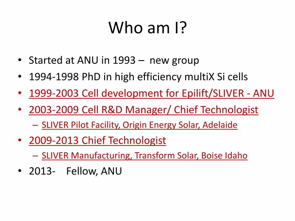
Who am I?
• Started at ANU in 1993 – new group
• 1994-1998 PhD in high efficiency multiX Si cells
• 1999-2003 Cell development for Epilift/SLIVER - ANU
• 2003-2009 Cell R&D Manager/ Chief Technologist
– SLIVER Pilot Facility, Origin Energy Solar, Adelaide
• 2009-2013 Chief Technologist
– SLIVER Manufacturing, Transform Solar, Boise Idaho
• 2013- Fellow, ANU
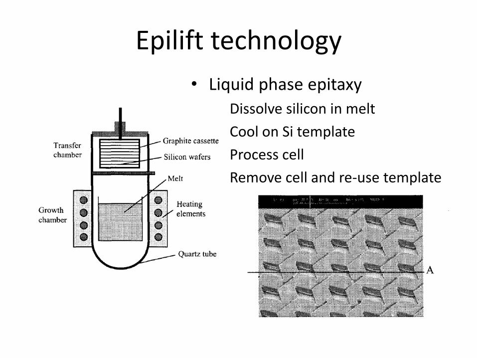
Epilift technology
• Liquid phase epitaxy
– Dissolve silicon in melt
– Cool on Si template
– Process cell
– Remove cell and re-use template
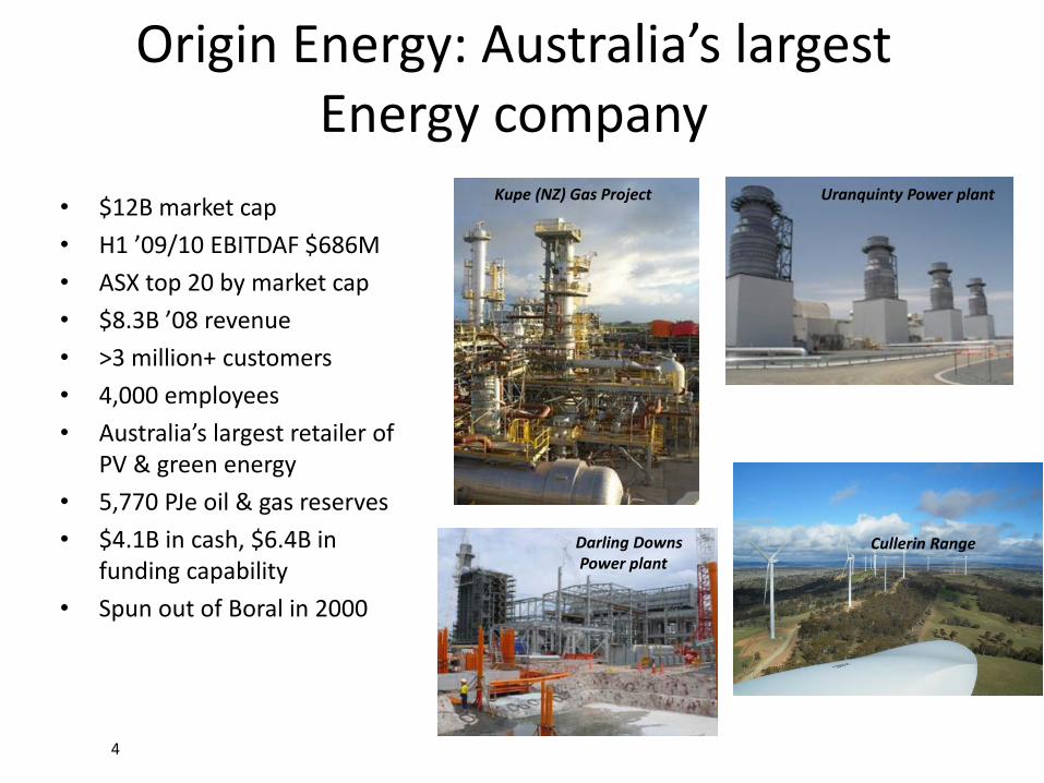
Darling Downs Power plant
Cullerin Range
4
Origin Energy: Australia’s largest Energy company
• $12B market cap
• H1 ’09/10 EBITDAF $686M
• ASX top 20 by market cap
• $8.3B ’08 revenue
• >3 million+ customers
• 4,000 employees
• Australia’s largest retailer of PV & green energy
• 5,770 PJe oil & gas reserves
• $4.1B in cash, $6.4B in funding capability
• Spun out of Boral in 2000
Kupe (NZ) Gas Project Uranquinty Power plant
0.1
1
10
100
1 10 100 1000 10000 100000 1000000
Mo
du
le P
rice
($
/W)
Cumulative Installed Capacity (MW)
$/W
ExperienceCurve
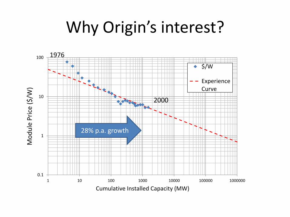
Why Origin’s interest?
1976
2000
28% p.a. growth
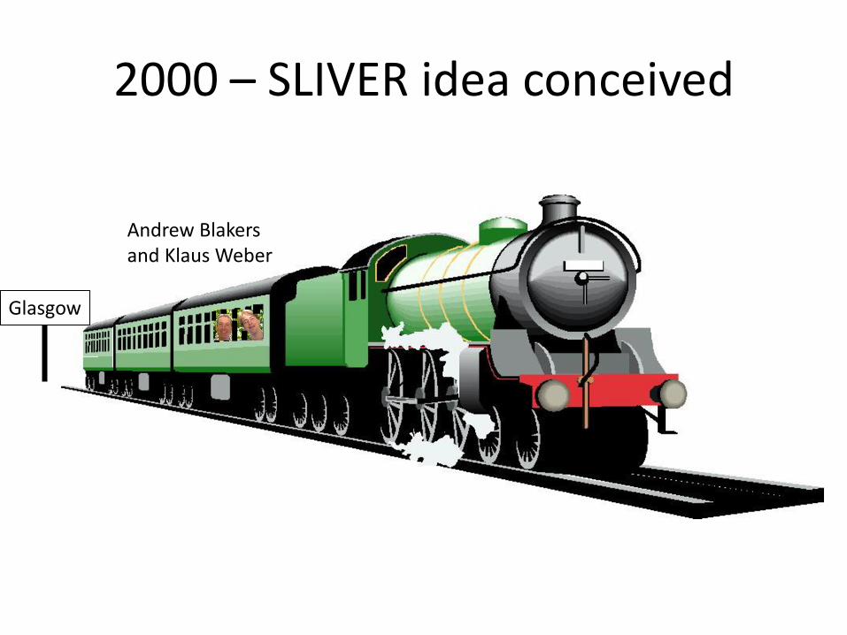
2000 – SLIVER idea conceived
Andrew Blakers and Klaus Weber
Glasgow
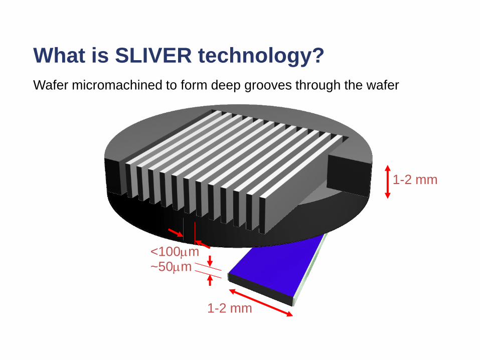
What is SLIVER technology?
1-2 mm
<100mm
Wafer micromachined to form deep grooves through the wafer
1-2 mm
~50mm
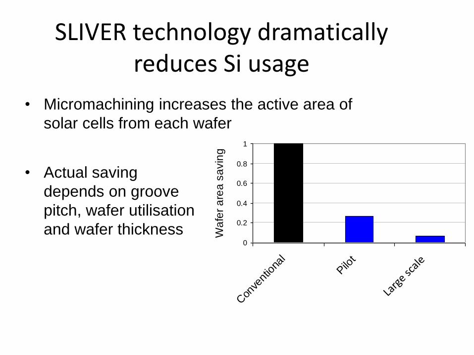
SLIVER technology dramatically reduces Si usage
• Micromachining increases the active area of
solar cells from each wafer
• Actual saving
depends on groove
pitch, wafer utilisation
and wafer thickness 0
0.2
0.4
0.6
0.8
1
Con
vent
iona
l
Pilo
t
Forse
eabl
e
Wa
fer
are
a s
avin
g
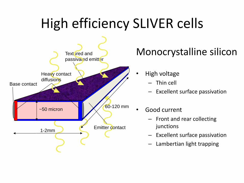
Textured and
passivated emitter
High efficiency SLIVER cells
Monocrystalline silicon
• High voltage
– Thin cell
– Excellent surface passivation
• Good current
– Front and rear collecting junctions
– Excellent surface passivation
– Lambertian light trapping
1-2mm
60-120 mm ~50 micron
Base contact
Emitter contact
Heavy contact
diffusions
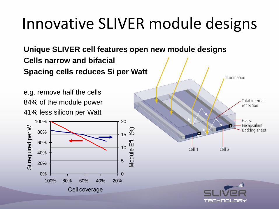
Innovative SLIVER module designs
Unique SLIVER cell features open new module designs
Cells narrow and bifacial
Spacing cells reduces Si per Watt
e.g. remove half the cells
84% of the module power
41% less silicon per Watt
0
5
10
15
20
20%40%60%80%100%
Cell coverage
Mo
du
le E
ff. (
%)
0%
20%
40%
60%
80%
100%
Si re
qu
ire
d p
er
W
0.1
1
10
100
1 10 100 1000 10000 100000 1000000
Mo
du
le P
rice
($
/W)
Cumulative Installed Capacity (MW)
$/W
ExperienceCurve
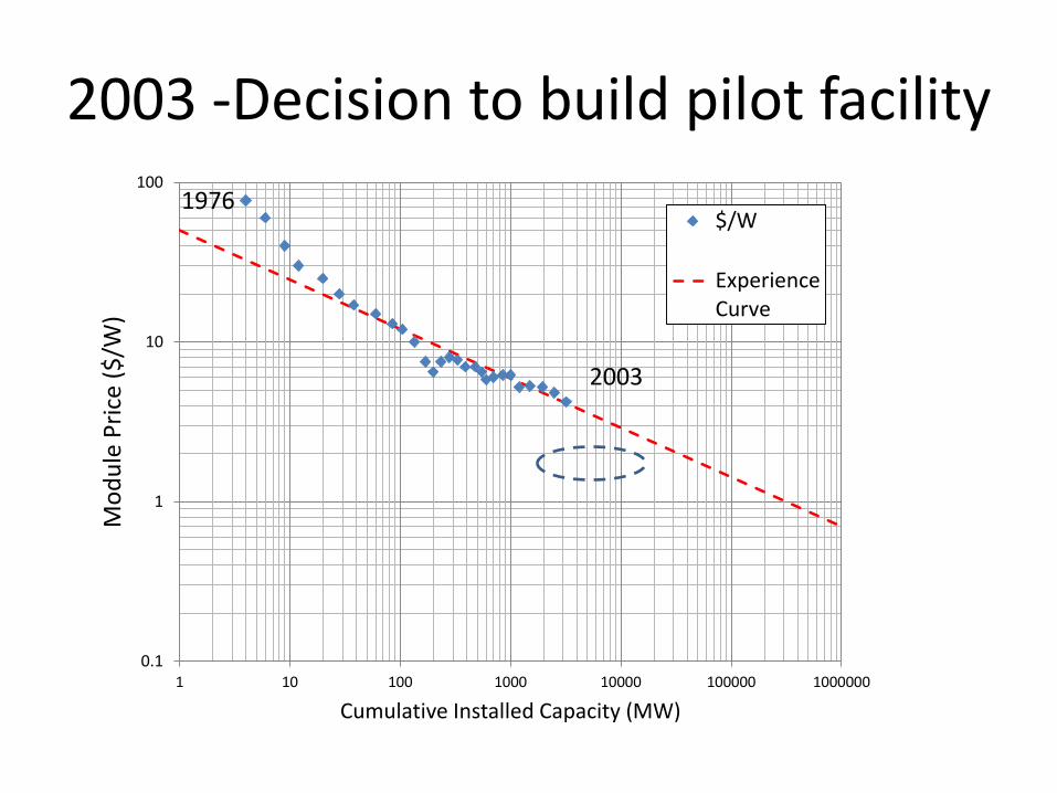
2003 -Decision to build pilot facility
1976
2003
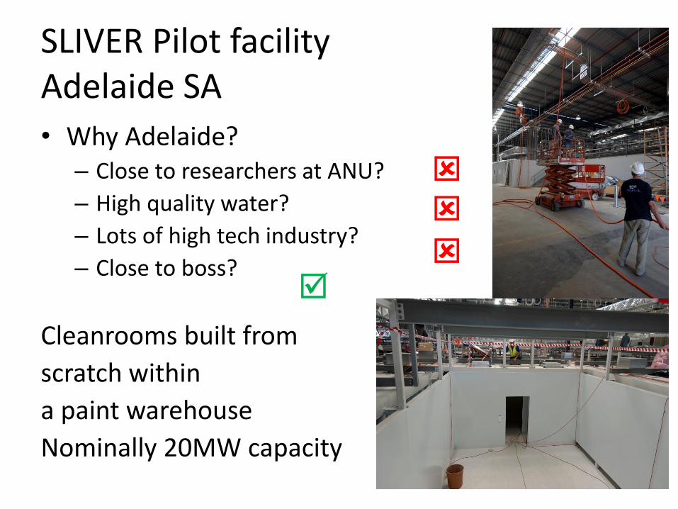
SLIVER Pilot facility Adelaide SA
• Why Adelaide? – Close to researchers at ANU?
– High quality water?
– Lots of high tech industry?
– Close to boss?
Cleanrooms built from
scratch within
a paint warehouse
Nominally 20MW capacity
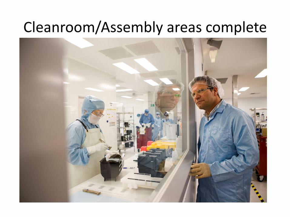
Cleanroom/Assembly areas complete
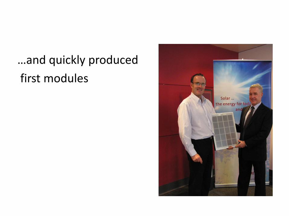
…and quickly produced
first modules

But the storm clouds were gathering
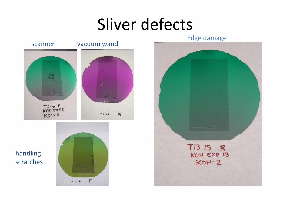
Sliver defects scanner
handling scratches
Edge damage vacuum wand
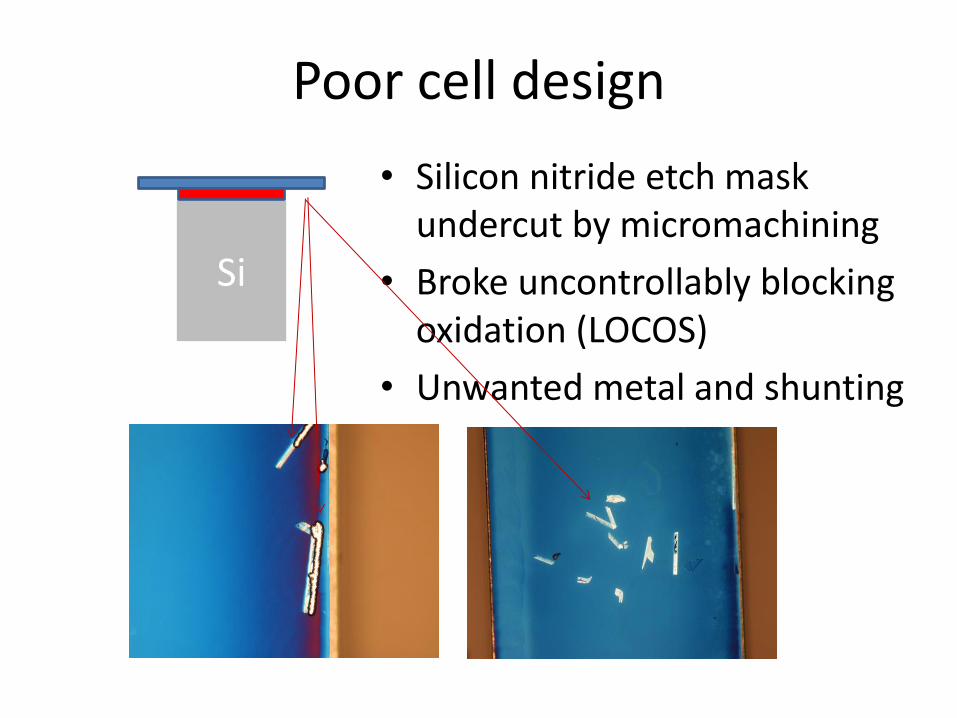
Poor cell design
• Silicon nitride etch mask undercut by micromachining
• Broke uncontrollably blocking oxidation (LOCOS)
• Unwanted metal and shunting
Si
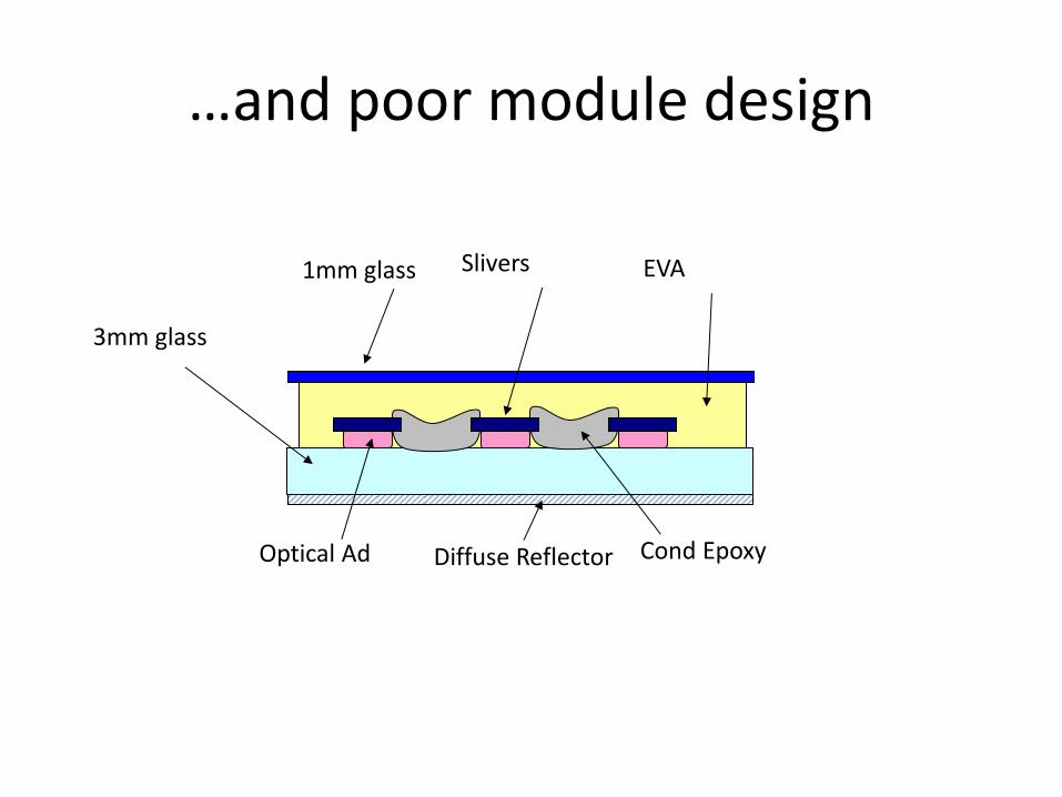
…and poor module design
1mm glass EVA Slivers
Optical Ad Cond Epoxy Diffuse Reflector
3mm glass
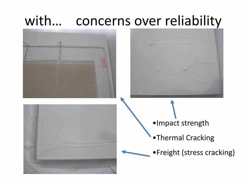
with… concerns over reliability
•Impact strength
•Thermal Cracking
•Freight (stress cracking)
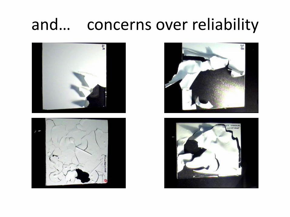
and… concerns over reliability
Automation
• Probably biggest challenge for commercialisation SLIVER technology
• Handle (very) large number of long thin parts
– Initial approach
• Throw dollars at the problem
• Go to experts in handling and robotics
–Custom automation companies
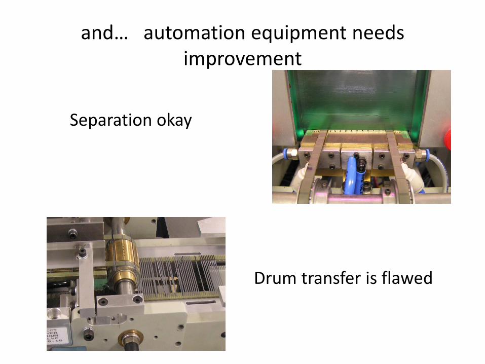
and… automation equipment needs improvement
Drum transfer is flawed
Separation okay
Back to basics
• Bring development back in house
• Cheap off the shelf SCARA robotic equipment
• Focus on design of head for interactions with SLIVER
• Slow down
– Understand what works and what doesn’t
To automation and back to in-house
• Gen 3 and 4 STP were back to automation companies
– Issues again with understanding SLIVER cells
• Gen 5 back in house
Gradually problems under control
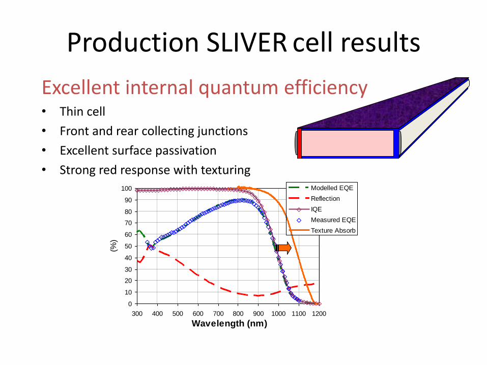
Production SLIVER cell results
Excellent internal quantum efficiency • Thin cell
• Front and rear collecting junctions
• Excellent surface passivation
• Strong red response with texturing
0
10
20
30
40
50
60
70
80
90
100
300 400 500 600 700 800 900 1000 1100 1200
Wavelength (nm)
(%)
Modelled EQE
Reflection
IQE
Measured EQE
Texture Absorb
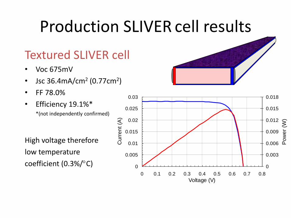
Production SLIVER cell results
Textured SLIVER cell • Voc 675mV
• Jsc 36.4mA/cm2 (0.77cm2)
• FF 78.0%
• Efficiency 19.1%* *(not independently confirmed)
High voltage therefore
low temperature
coefficient (0.3%/C) 0
0.005
0.01
0.015
0.02
0.025
0.03
0 0.1 0.2 0.3 0.4 0.5 0.6 0.7 0.8
Voltage (V)
Cu
rre
nt
(A)
0
0.003
0.006
0.009
0.012
0.015
0.018
Po
we
r (W
)
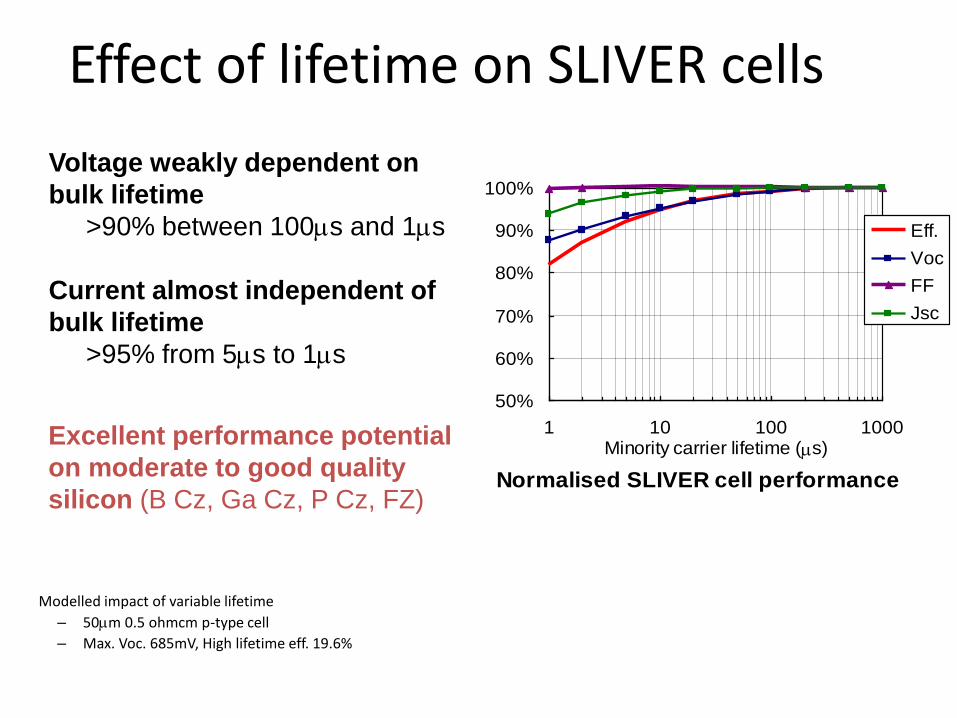
Effect of lifetime on SLIVER cells
Modelled impact of variable lifetime
– 50mm 0.5 ohmcm p-type cell
– Max. Voc. 685mV, High lifetime eff. 19.6%
Normalised SLIVER cell performance
50%
60%
70%
80%
90%
100%
1 10 100 1000Minority carrier lifetime (ms)
Eff.
Voc
FF
Jsc
Voltage weakly dependent on
bulk lifetime
>90% between 100ms and 1ms
Current almost independent of
bulk lifetime
>95% from 5ms to 1ms
Excellent performance potential
on moderate to good quality
silicon (B Cz, Ga Cz, P Cz, FZ)
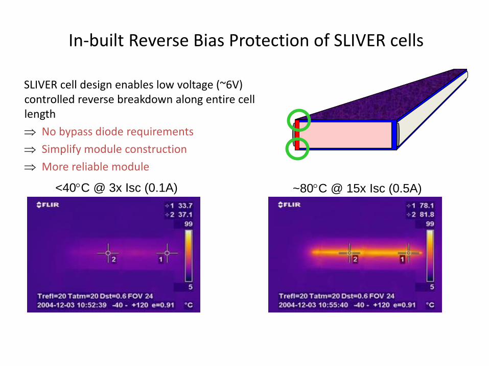
~80C @ 15x Isc (0.5A)
In-built Reverse Bias Protection of SLIVER cells
SLIVER cell design enables low voltage (~6V) controlled reverse breakdown along entire cell length
No bypass diode requirements
Simplify module construction
More reliable module
<40C @ 3x Isc (0.1A)
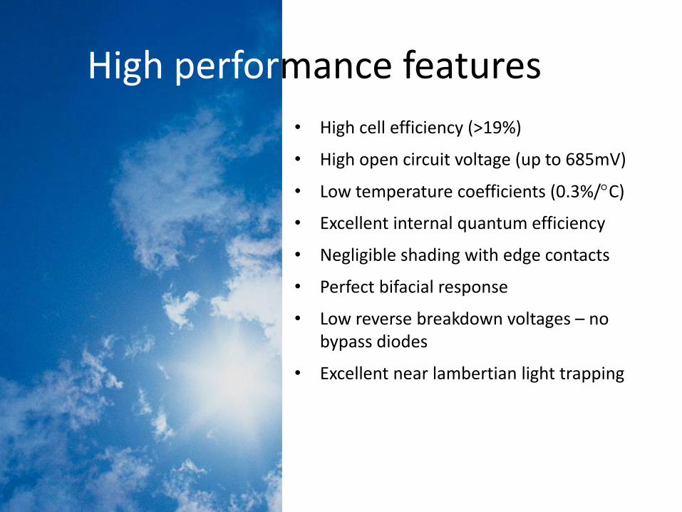
• High cell efficiency (>19%)
• High open circuit voltage (up to 685mV)
• Low temperature coefficients (0.3%/C)
• Excellent internal quantum efficiency
• Negligible shading with edge contacts
• Perfect bifacial response
• Low reverse breakdown voltages – no bypass diodes
• Excellent near lambertian light trapping
High performance features
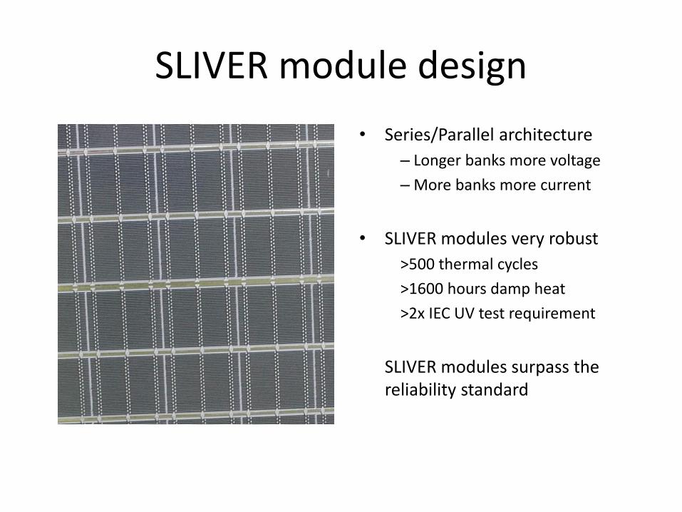
SLIVER module design
• Series/Parallel architecture
– Longer banks more voltage
– More banks more current
• SLIVER modules very robust
>500 thermal cycles
>1600 hours damp heat
>2x IEC UV test requirement
SLIVER modules surpass the reliability standard
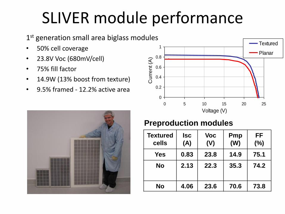
SLIVER module performance 1st generation small area biglass modules
• 50% cell coverage
• 23.8V Voc (680mV/cell)
• 75% fill factor
• 14.9W (13% boost from texture)
• 9.5% framed - 12.2% active area
0
0.2
0.4
0.6
0.8
1
0 5 10 15 20 25
Voltage (V)
Cu
rre
nt (A
)
Textured
Planar
Textured
cells
Isc
(A)
Voc
(V)
Pmp
(W)
FF
(%)
Yes 0.83 23.8 14.9 75.1
No 2.13 22.3 35.3 74.2
No 4.06 23.6 70.6 73.8
Preproduction modules
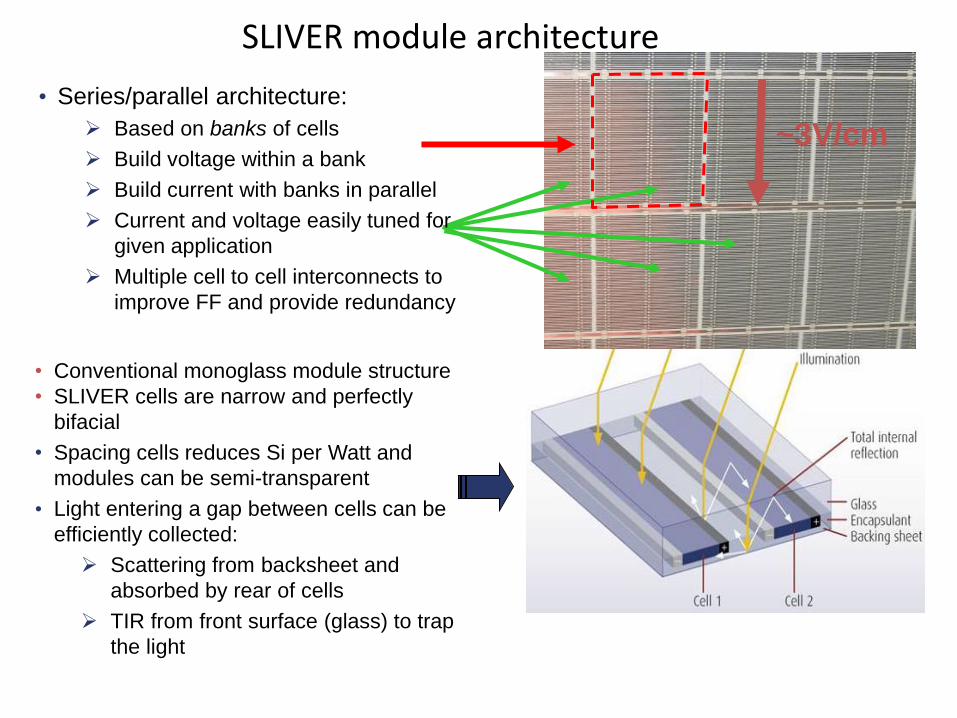
SLIVER module architecture
~3V/cm
• Series/parallel architecture:
Based on banks of cells
Build voltage within a bank
Build current with banks in parallel
Current and voltage easily tuned for
given application
Multiple cell to cell interconnects to
improve FF and provide redundancy
• Conventional monoglass module structure
• SLIVER cells are narrow and perfectly
bifacial
• Spacing cells reduces Si per Watt and
modules can be semi-transparent
• Light entering a gap between cells can be
efficiently collected:
Scattering from backsheet and
absorbed by rear of cells
TIR from front surface (glass) to trap
the light
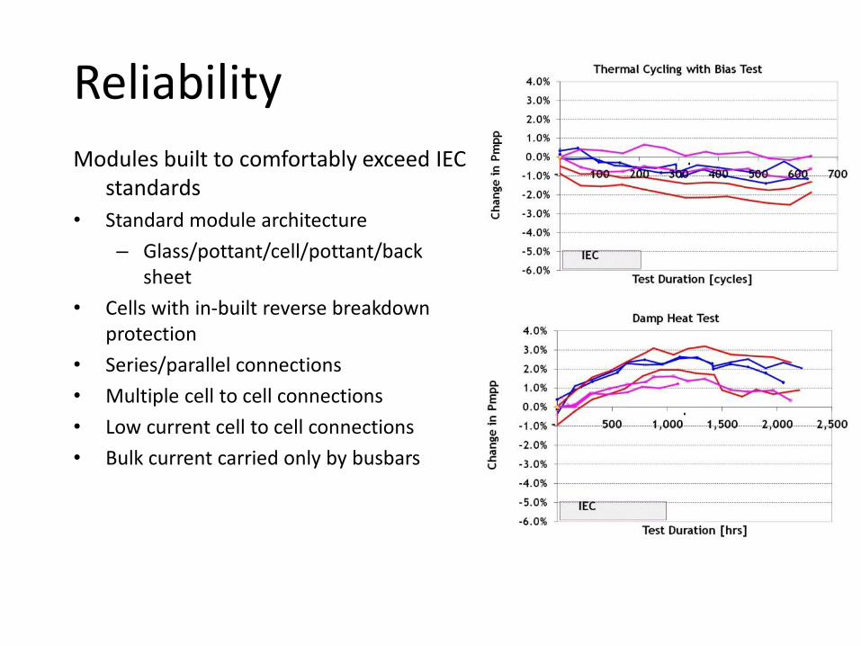
Reliability
Modules built to comfortably exceed IEC standards
• Standard module architecture
– Glass/pottant/cell/pottant/back sheet
• Cells with in-built reverse breakdown protection
• Series/parallel connections
• Multiple cell to cell connections
• Low current cell to cell connections
• Bulk current carried only by busbars
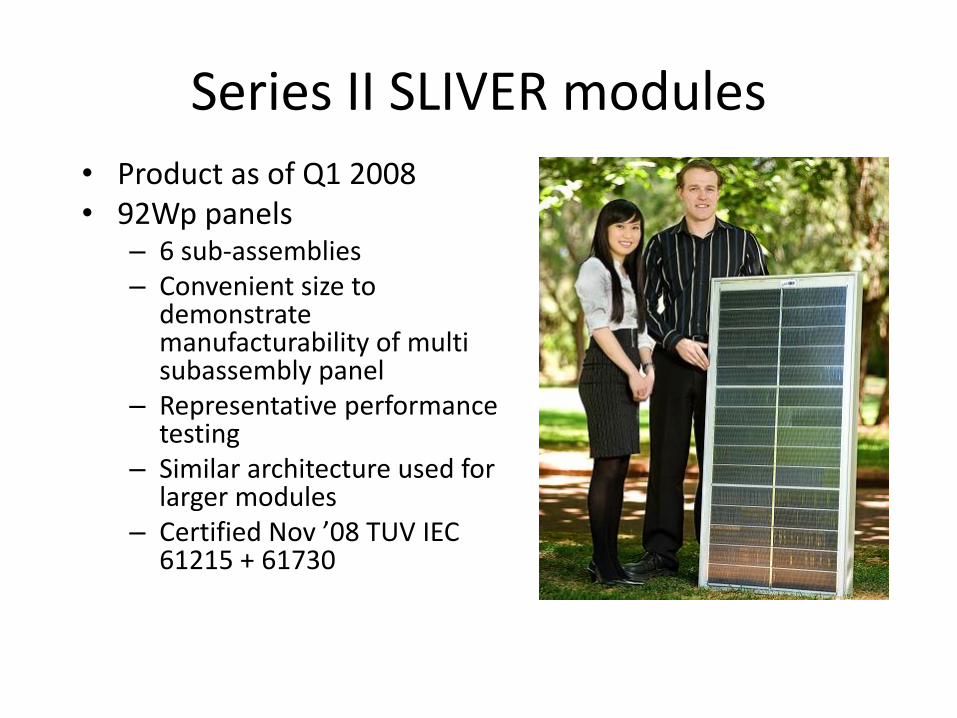
Series II SLIVER modules
• Product as of Q1 2008 • 92Wp panels
– 6 sub-assemblies – Convenient size to
demonstrate manufacturability of multi subassembly panel
– Representative performance testing
– Similar architecture used for larger modules
– Certified Nov ’08 TUV IEC 61215 + 61730
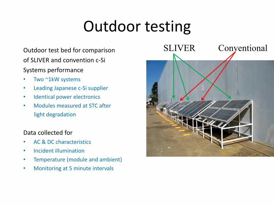
Outdoor testing Outdoor test bed for comparison
of SLIVER and convention c-Si
Systems performance
• Two ~1kW systems
• Leading Japanese c-Si supplier
• Identical power electronics
• Modules measured at STC after
light degradation
Data collected for
• AC & DC characteristics
• Incident illumination
• Temperature (module and ambient)
• Monitoring at 5 minute intervals
SLIVER Conventional
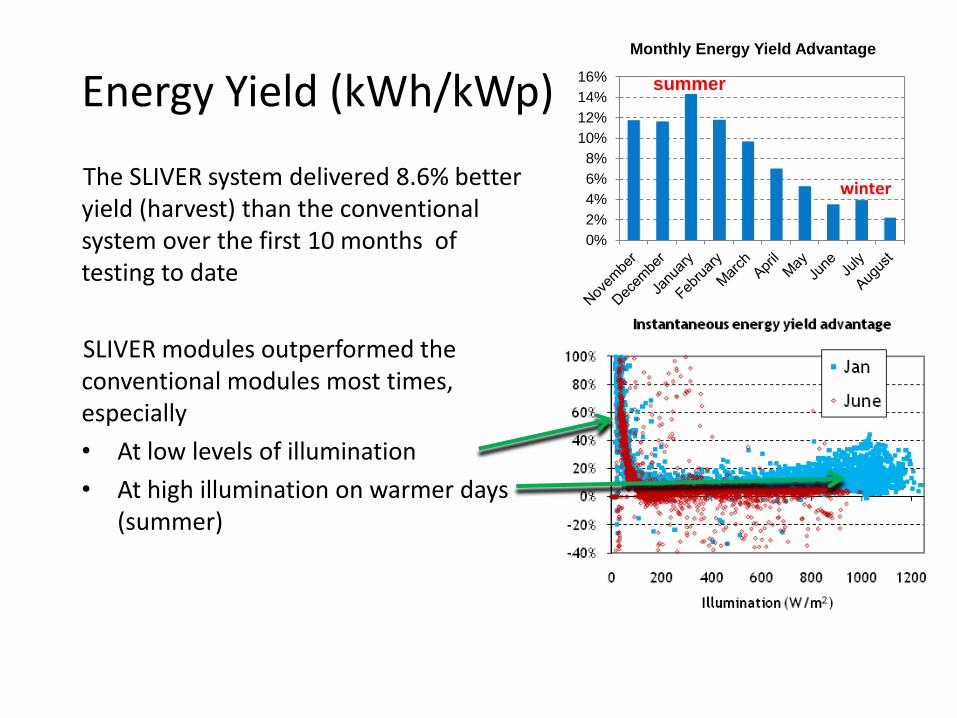
Energy Yield (kWh/kWp)
The SLIVER system delivered 8.6% better yield (harvest) than the conventional system over the first 10 months of testing to date
SLIVER modules outperformed the conventional modules most times, especially
• At low levels of illumination
• At high illumination on warmer days (summer)
0%
2%
4%
6%
8%
10%
12%
14%
16%
Monthly Energy Yield Advantage
summer
winter
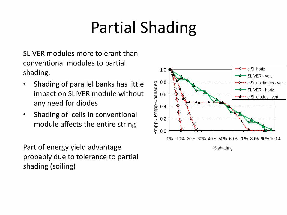
Partial Shading
SLIVER modules more tolerant than conventional modules to partial shading.
• Shading of parallel banks has little impact on SLIVER module without any need for diodes
• Shading of cells in conventional module affects the entire string
Part of energy yield advantage probably due to tolerance to partial shading (soiling)
0.0
0.2
0.4
0.6
0.8
1.0
0% 10% 20% 30% 40% 50% 60% 70% 80% 90% 100%
Pm
pp
/ P
mp
p-u
nshad
ed
% shading
c-Si, horiz
SLIVER - vert
c-Si, no diodes - vert
SLIVER - horiz
c-Si, diodes - vert
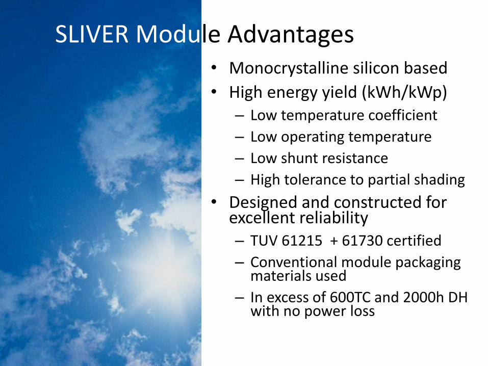
• Monocrystalline silicon based
• High energy yield (kWh/kWp) – Low temperature coefficient
– Low operating temperature
– Low shunt resistance
– High tolerance to partial shading
• Designed and constructed for excellent reliability – TUV 61215 + 61730 certified
– Conventional module packaging materials used
– In excess of 600TC and 2000h DH with no power loss
SLIVER Module Advantages
0.1
1
10
100
1 10 100 1000 10000 100000 1000000
Mo
du
le P
rice
($
/W)
Cumulative Installed Capacity (MW)
$/W
ExperienceCurve
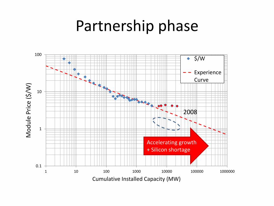
Accelerating growth + Silicon shortage
Partnership phase
2008
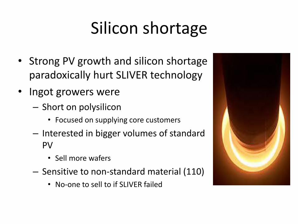
Silicon shortage
• Strong PV growth and silicon shortage paradoxically hurt SLIVER technology
• Ingot growers were
– Short on polysilicon • Focused on supplying core customers
– Interested in bigger volumes of standard PV • Sell more wafers
– Sensitive to non-standard material (110) • No-one to sell to if SLIVER failed
Why partner?
• Understanding and mitigating risk
• Origin very willing to take risks
– Every exploration/ drilling project has good chance of failure
– Typically shared with partners
– No feel for manufacturing
• Therefore risk averse
• Criteria
– Semiconductor/ solar/ technology company
– Manufacturing experience
• Origin is an energy company
– Similar scale to Origin
• Genuine partnership
• Neither side too big to bully the other
– Lower cost access materials
• Particularly module
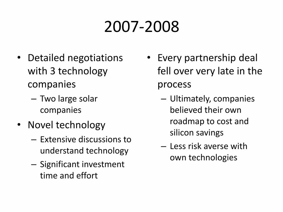
2007-2008
• Detailed negotiations with 3 technology companies
– Two large solar companies
• Novel technology
– Extensive discussions to understand technology
– Significant investment time and effort
• Every partnership deal fell over very late in the process
– Ultimately, companies believed their own roadmap to cost and silicon savings
– Less risk averse with own technologies
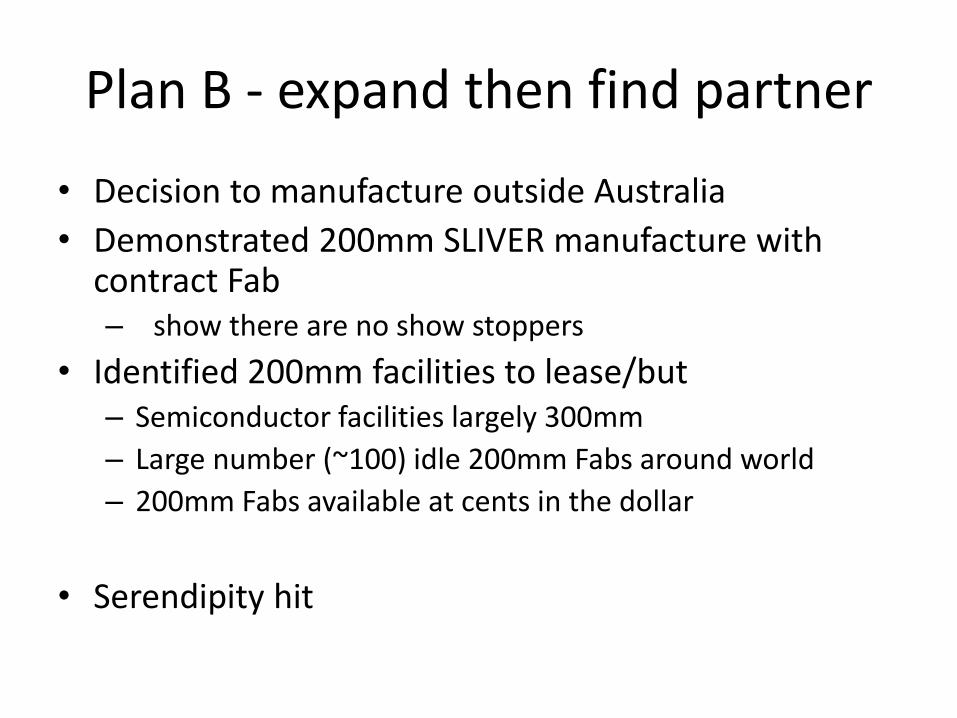
Plan B - expand then find partner
• Decision to manufacture outside Australia
• Demonstrated 200mm SLIVER manufacture with contract Fab – show there are no show stoppers
• Identified 200mm facilities to lease/but – Semiconductor facilities largely 300mm
– Large number (~100) idle 200mm Fabs around world
– 200mm Fabs available at cents in the dollar
• Serendipity hit
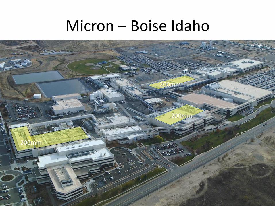
Micron – Boise Idaho
200mm
200mm
200mm
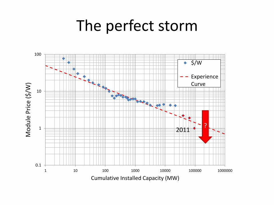
The perfect storm
0.1
1
10
100
1 10 100 1000 10000 100000 1000000
Mo
du
le P
rice
($
/W)
Cumulative Installed Capacity (MW)
$/W
ExperienceCurve
2011 ?
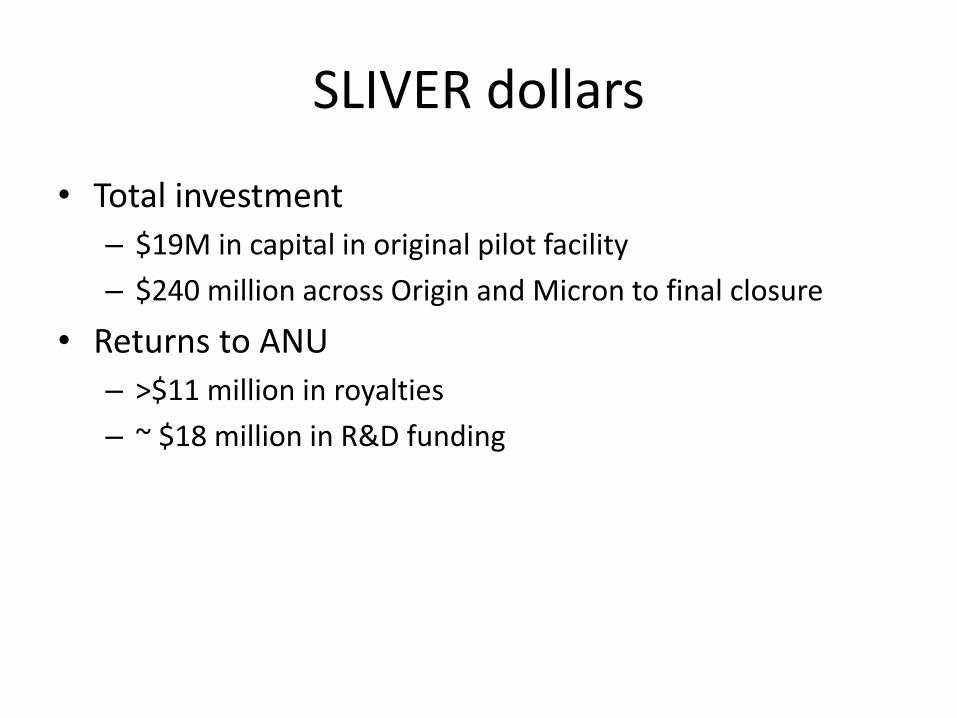
SLIVER dollars
• Total investment
– $19M in capital in original pilot facility
– $240 million across Origin and Micron to final closure
• Returns to ANU
– >$11 million in royalties
– ~ $18 million in R&D funding
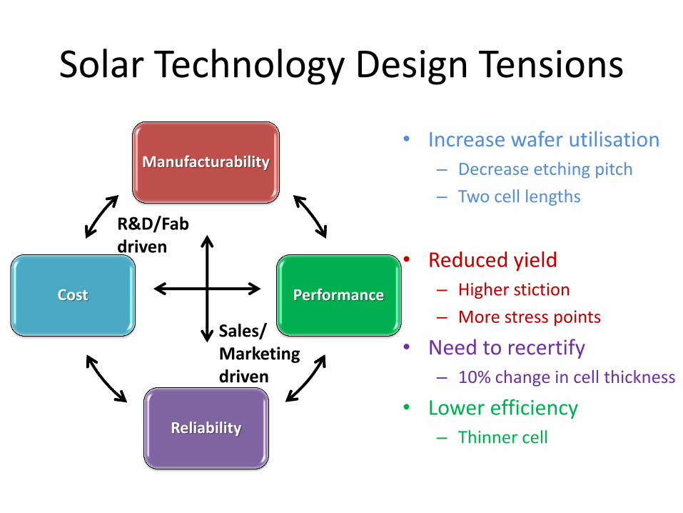
Solar Technology Design Tensions
• Increase wafer utilisation – Decrease etching pitch
– Two cell lengths
• Reduced yield – Higher stiction
– More stress points
• Need to recertify – 10% change in cell thickness
• Lower efficiency – Thinner cell
Manufacturability
Performance
Reliability
Cost
R&D/Fab driven
Sales/ Marketing driven
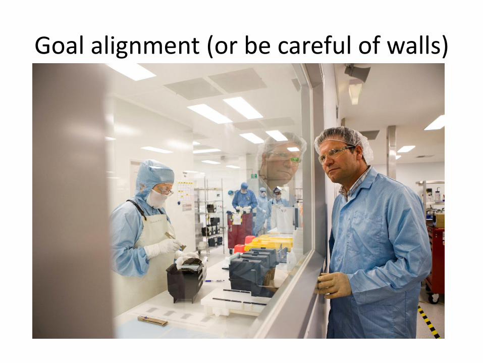
Goal alignment (or be careful of walls)
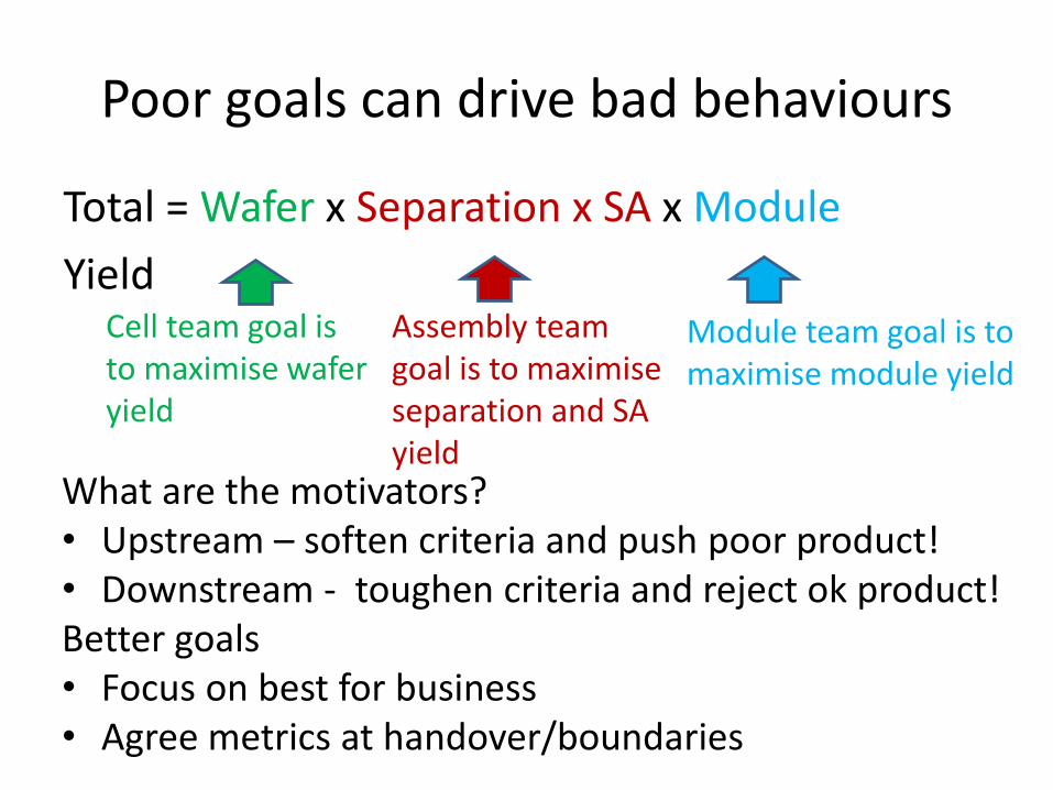
Poor goals can drive bad behaviours
Total = Wafer x Separation x SA x Module
Yield
Cell team goal is to maximise wafer yield
Assembly team goal is to maximise separation and SA yield
Module team goal is to maximise module yield
What are the motivators? • Upstream – soften criteria and push poor product! • Downstream - toughen criteria and reject ok product! Better goals • Focus on best for business • Agree metrics at handover/boundaries
Start Up vs Big Business
• Cash poor
– Motivated to be fast
• Risk takers
– Good enough
• Everything from scratch
– Need to invent it all
• Strong team ethos
– Us against the world
• Deep pockets
• Risk averse
– Slow to move
• Systems in place
– E.g. safety
• Door opener
– access to suppliers, etc
Don’t underestimate need for champions

Biggest satisfaction
• Solving technical challenges to move from lab to manufacturing – Deepest, narrowest
micromachining
– Vastly simplified cell process
– STP
– Sub assembly development
– Demo of >190W wafer
– Reliable module product
– Building good R&D teams
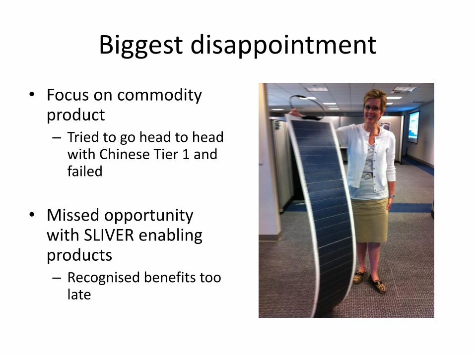
Biggest disappointment
• Focus on commodity product – Tried to go head to head
with Chinese Tier 1 and failed
• Missed opportunity with SLIVER enabling products – Recognised benefits too
late