Embed Size (px)
Citation preview
Slide Set 3, Slide 1
Slide Set 3
Pass Transistor Logic / Transmission Gates
Steve WiltonDept. of ECE
University of British [email protected]

Slide Set 3, Slide 2
Overview
• Reading– Wolf 3.4, 4.7
• IntroductionIn the last lecture, we talked about how simple CMOS gates can be built. In this lecture, we will talk about another way to implement logic functions using transistors: pass-transistor logic (NMOS only) and transmission-gate logic (NMOS and CMOS transistors). For some types of functions, this can lead to much more efficient implementations than using gates.
Slide Set 3, Slide 3
Switch Networks
Board Notes:
- Series Connections, Parallel Connections
- Multiplexer circuit
Slide Set 3, Slide 4
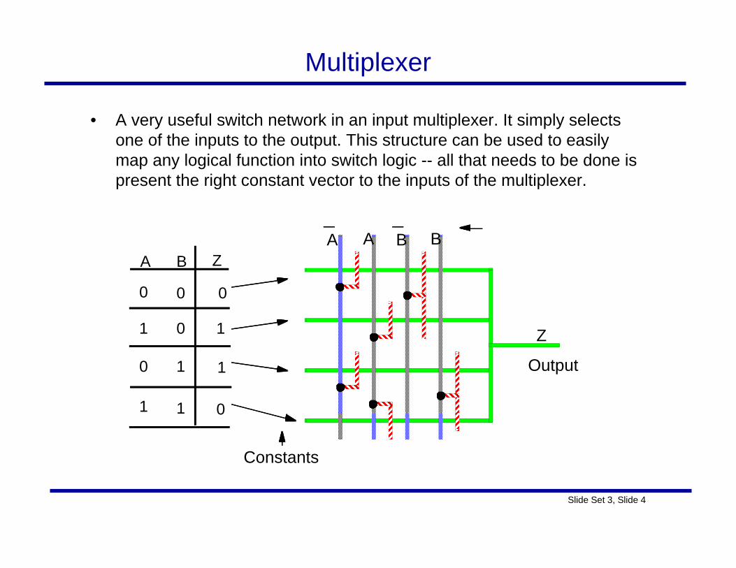
Multiplexer
• A very useful switch network in an input multiplexer. It simply selects one of the inputs to the output. This structure can be used to easily map any logical function into switch logic -- all that needs to be done is present the right constant vector to the inputs of the multiplexer.
A BA BA B Z
0 0 0
1 0 1
0 1 1
1 1 0
Z
Constants
Output
Slide Set 3, Slide 5
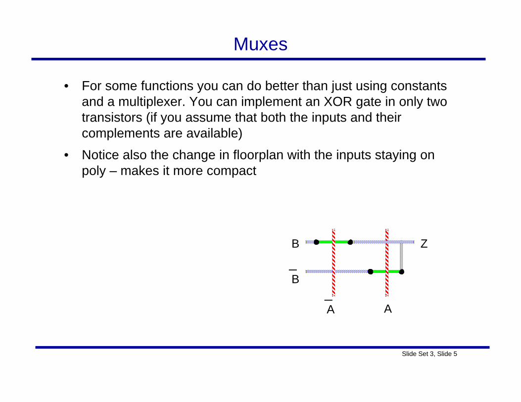
Muxes
• For some functions you can do better than just using constants and a multiplexer. You can implement an XOR gate in only two transistors (if you assume that both the inputs and their complements are available)
• Notice also the change in floorplan with the inputs staying on poly – makes it more compact
AA
Z
B
B
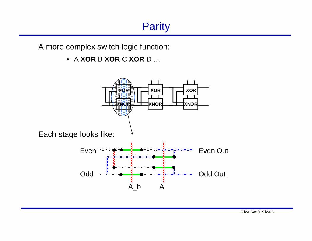
Slide Set 3, Slide 6
Even
Odd
A_b A
Even Out
Odd Out
Each stage looks like:
Parity
XOR
XNOR
XOR
XNOR
XOR
XNOR
A more complex switch logic function:• A XOR B XOR C XOR D …
Slide Set 3, Slide 7
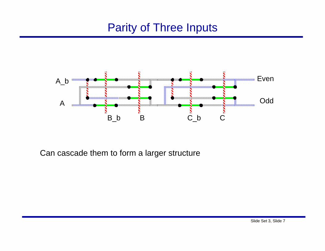
Parity of Three Inputs
Can cascade them to form a larger structure
C_b CB_b B
A_b
A
Even
Odd
Slide Set 3, Slide 8
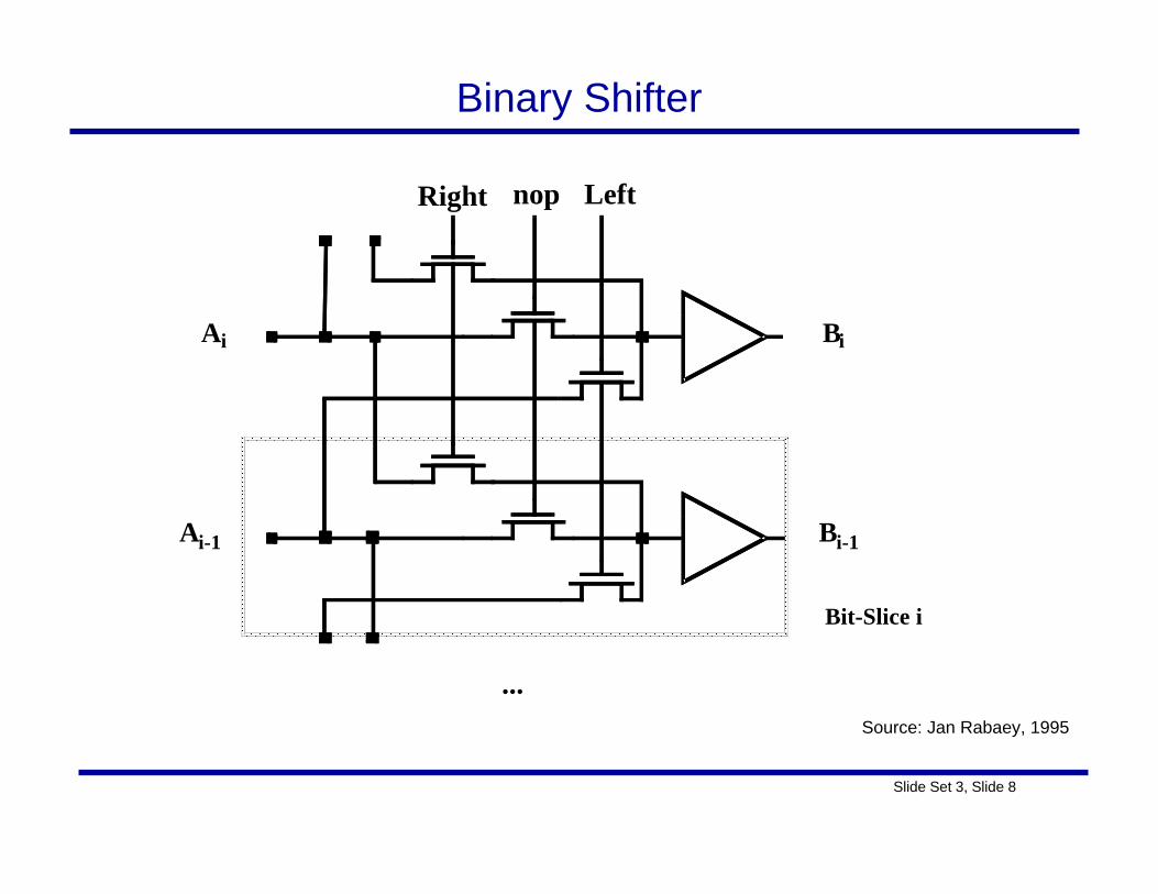
Binary Shifter
Ai
Ai-1
Bi
Bi-1
Right Leftnop
Bit-Slice i
...Source: Jan Rabaey, 1995
Slide Set 3, Slide 9
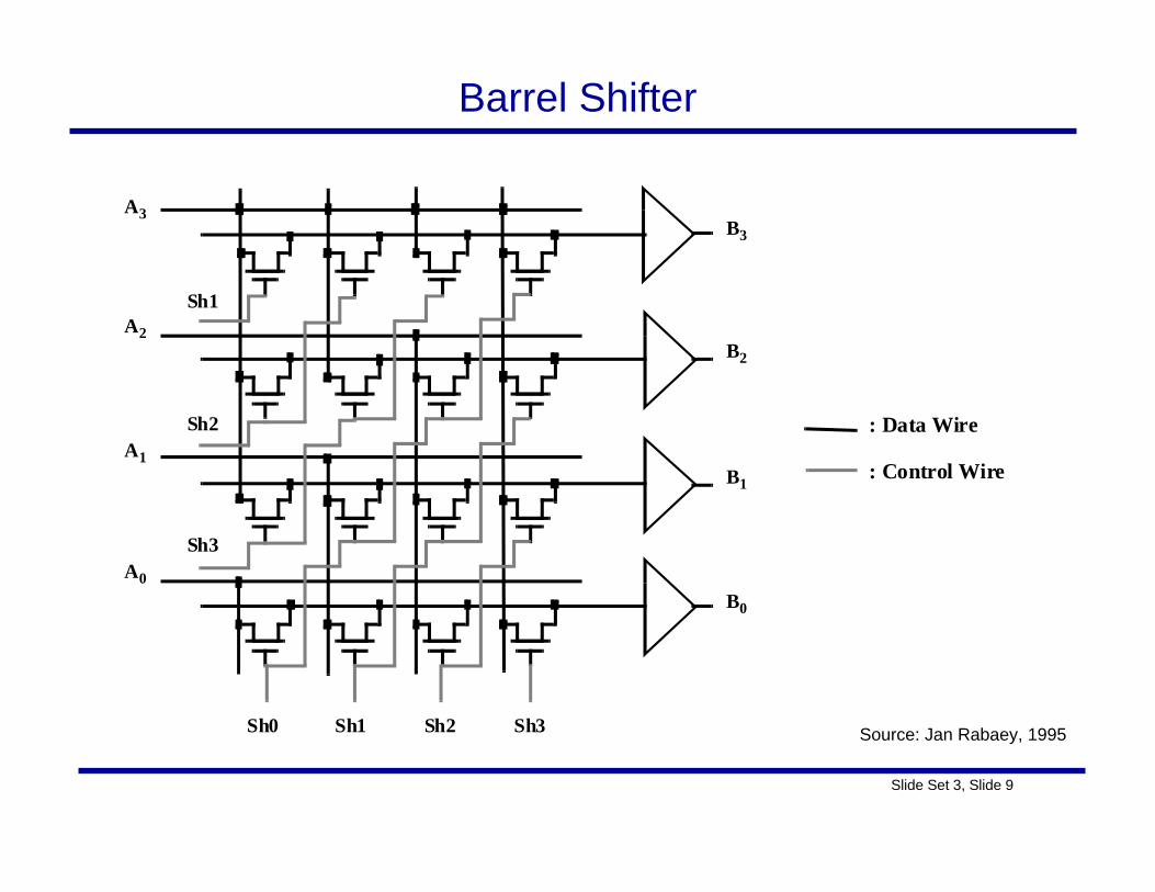
Barrel Shifter
Sh3Sh2Sh1Sh0
Sh3
Sh2
Sh1
A3
A2
A1
A0
B3
B2
B1
B0
: Control Wire
: Data Wire
Source: Jan Rabaey, 1995
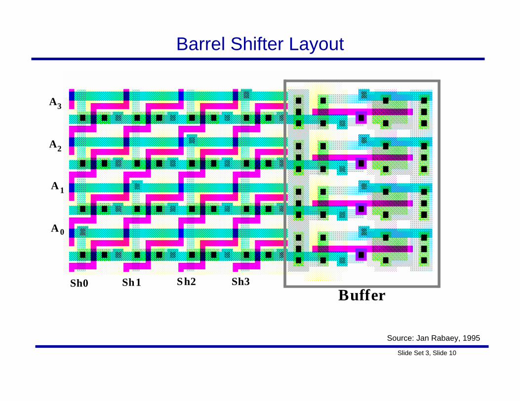
Slide Set 3, Slide 10
Barrel Shifter Layout
BufferSh3Sh2Sh1Sh0
A3
A2
A 1
A 0
Source: Jan Rabaey, 1995
Slide Set 3, Slide 11
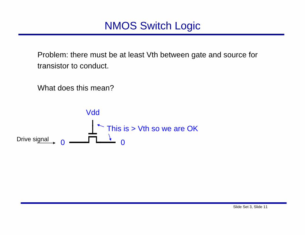
NMOS Switch Logic
Problem: there must be at least Vth between gate and source fortransistor to conduct.
What does this mean?
Vdd
0 0Drive signalThis is > Vth so we are OK
Slide Set 3, Slide 12
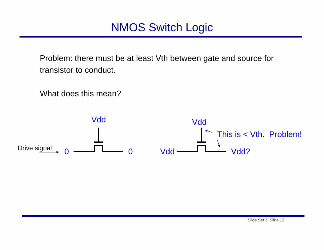
NMOS Switch Logic
Problem: there must be at least Vth between gate and source fortransistor to conduct.
What does this mean?
Vdd
0 0Drive signal
This is < Vth. Problem!
Vdd Vdd?
Vdd
Slide Set 3, Slide 13
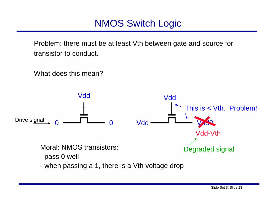
NMOS Switch Logic
Problem: there must be at least Vth between gate and source fortransistor to conduct.
What does this mean?
Vdd
0 0Drive signal
This is < Vth. Problem!
Vdd Vdd?
Vdd
Vdd-Vth
Moral: NMOS transistors:- pass 0 well- when passing a 1, there is a Vth voltage drop
Degraded signal
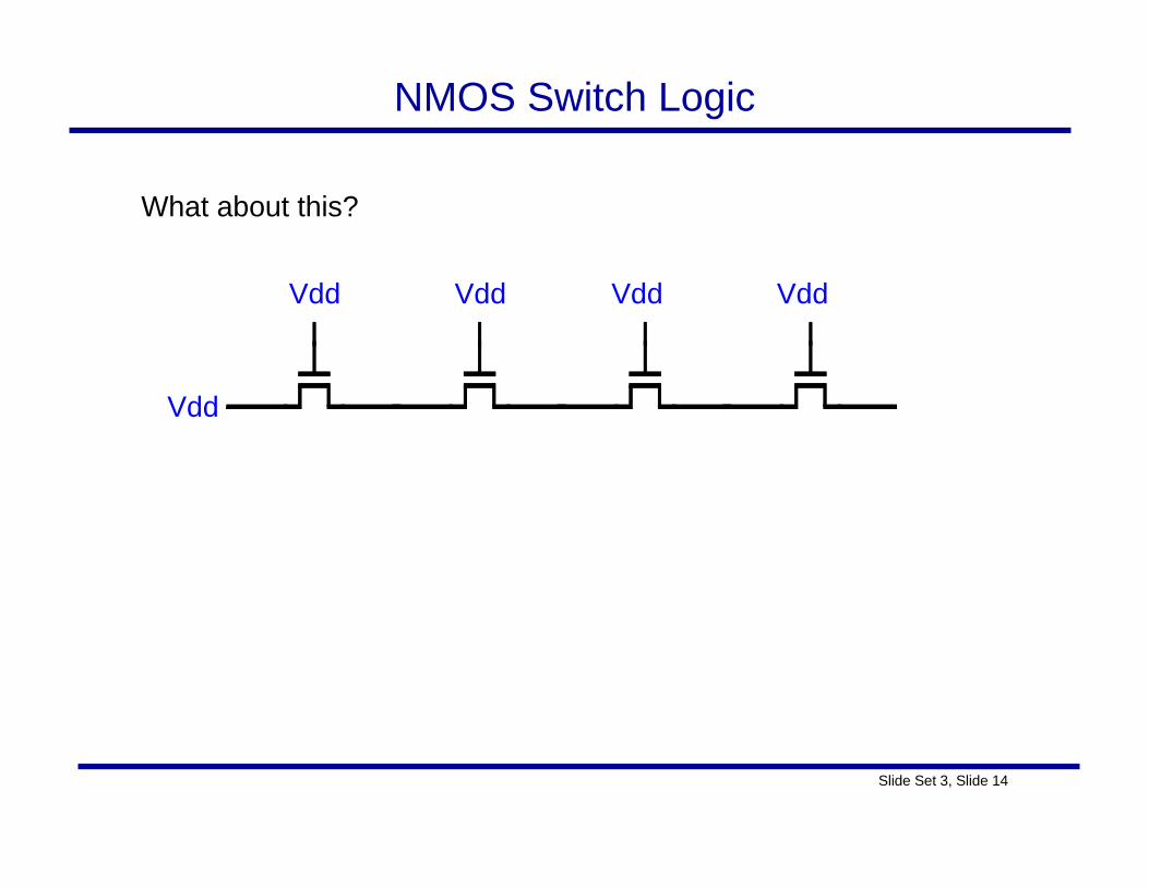
Slide Set 3, Slide 14
NMOS Switch Logic
What about this?
Vdd
Vdd
Vdd Vdd Vdd
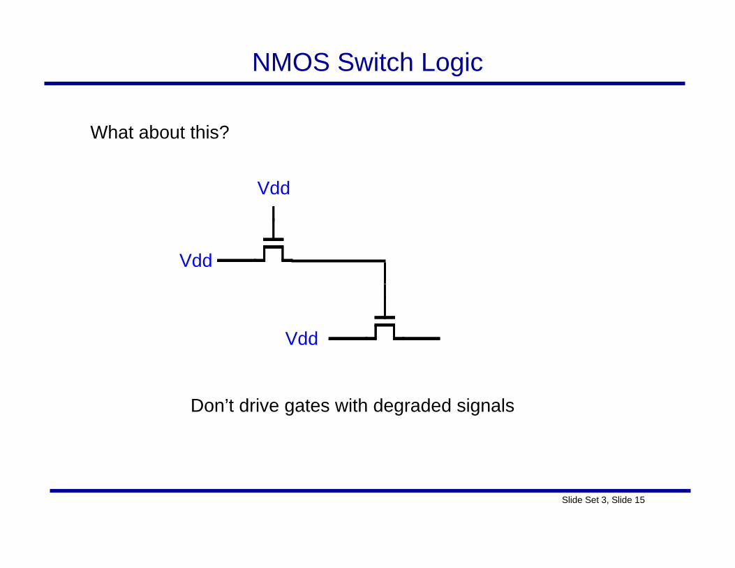
Slide Set 3, Slide 15
NMOS Switch Logic
What about this?
Vdd
Vdd
Don’t drive gates with degraded signals
Vdd
Slide Set 3, Slide 16
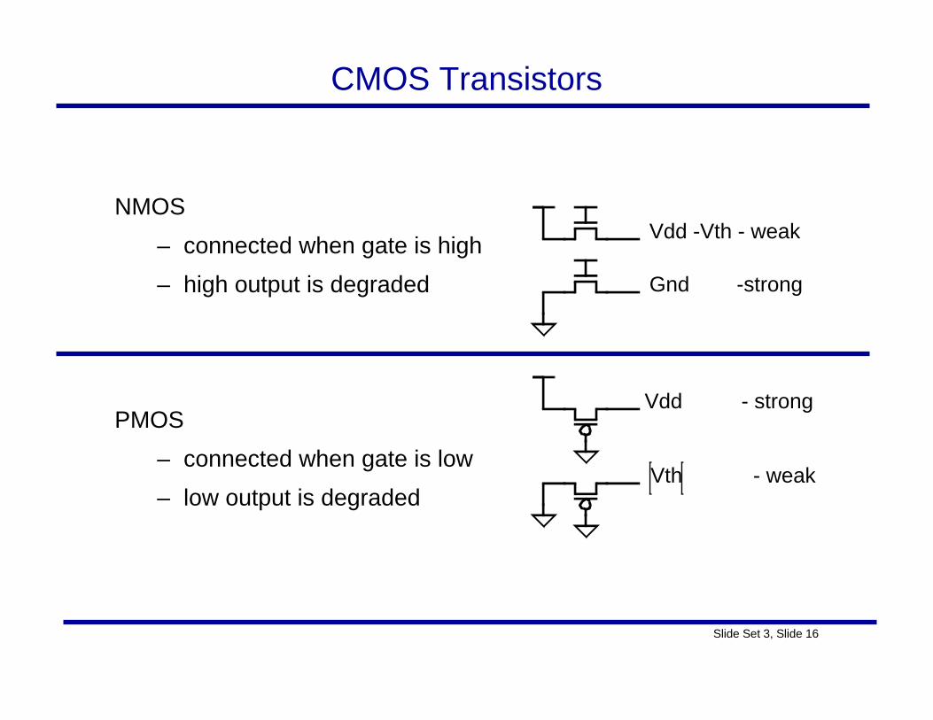
CMOS Transistors
NMOS– connected when gate is high– high output is degraded
PMOS– connected when gate is low– low output is degraded
Vdd -Vth - weak
Gnd -strong
Vdd - strong
Vth - weak
Slide Set 3, Slide 17
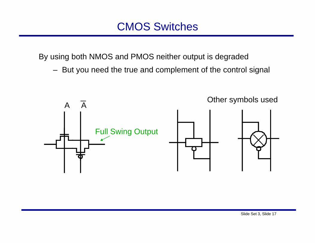
CMOS Switches
By using both NMOS and PMOS neither output is degraded– But you need the true and complement of the control signal
Full Swing Output
A AOther symbols used
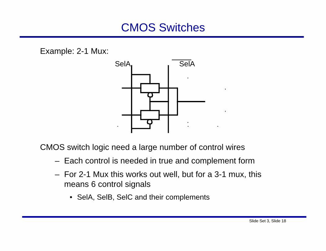
Slide Set 3, Slide 18
CMOS Switches
Example: 2-1 Mux:
CMOS switch logic need a large number of control wires– Each control is needed in true and complement form– For 2-1 Mux this works out well, but for a 3-1 mux, this
means 6 control signals• SelA, SelB, SelC and their complements
SelA SelA
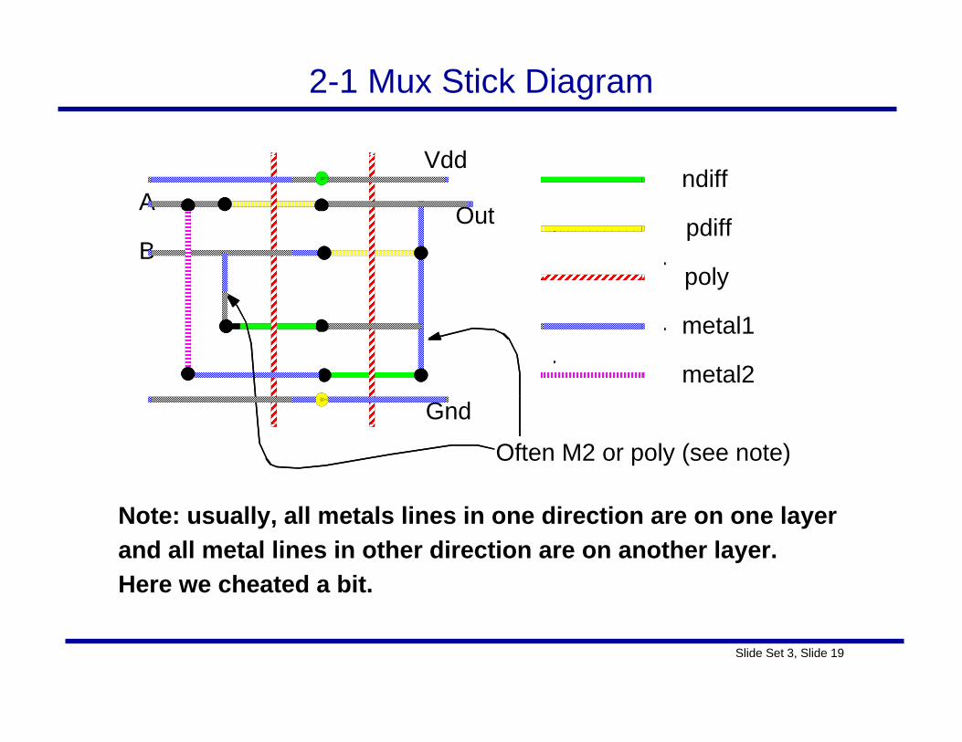
Slide Set 3, Slide 19
2-1 Mux Stick Diagram
Note: usually, all metals lines in one direction are on one layerand all metal lines in other direction are on another layer.Here we cheated a bit.
Often M2 or poly (see note)
ndiff
pdiff
poly
metal1
metal2
Vdd
Out
Gnd
A
B
Slide Set 3, Slide 20
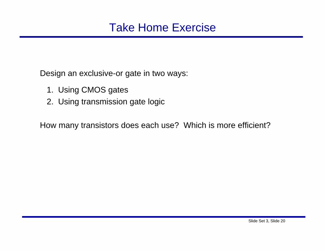
Take Home Exercise
Design an exclusive-or gate in two ways:
1. Using CMOS gates 2. Using transmission gate logic
How many transistors does each use? Which is more efficient?

![High Performance Logic Style with Constant Delay ... · traditional static and pass transistor CMOS logic ... domino (NORA domino) [3], zipper ... trendy logic style in high-performance](https://img.pdfslide.us/doc/110x75/5b7b4e627f8b9adb4c8c5a93/high-performance-logic-style-with-constant-delay-traditional-static-and.jpg)