Embed Size (px)
Citation preview
Solid-State IDE Flash Drive (No Moving Parts)
Capacity: 128MB - 16GB
ATA-5 Compatible
ATA Transfer modes:
PIO 0-6, MWDMA 0-4
Force PIO Mode available for applications requiring PIO Modes only
Supports TrueIDE and PC Card Memory and I/O Modes
Form Factors:
2.5-inch Ruggedized Enclosure with 44-pin IDE Connector
Endurance Guarantee of 2,000,000 Write/Erase Cycles
Master or Slave Select by Jumper
5V or 3.3V Power Supply
Commercial and Industrial Operating Temperature Range
5-Byte Detection, 4-Byte Correction ECC Engine
10 Year Data Retention
RoHS-6 Compliant
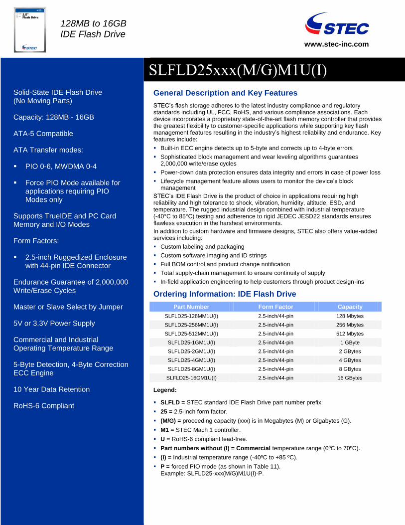
SLFLD25xxx(M/G)M1U(I)
128MB to 16GB IDE Flash Drive
General Description and Key Features
STEC’s flash storage adheres to the latest industry compliance and regulatory standards including UL, FCC, RoHS, and various compliance associations. Each device incorporates a proprietary state-of-the-art flash memory controller that provides the greatest flexibility to customer-specific applications while supporting key flash management features resulting in the industry’s highest reliability and endurance. Key features include:
Built-in ECC engine detects up to 5-byte and corrects up to 4-byte errors
Sophisticated block management and wear leveling algorithms guarantees 2,000,000 write/erase cycles
Power-down data protection ensures data integrity and errors in case of power loss
Lifecycle management feature allows users to monitor the device’s block management
STEC’s IDE Flash Drive is the product of choice in applications requiring high reliability and high tolerance to shock, vibration, humidity, altitude, ESD, and temperature. The rugged industrial design combined with industrial temperature (40°C to 85°C) testing and adherence to rigid JEDEC JESD22 standards ensures flawless execution in the harshest environments.
In addition to custom hardware and firmware designs, STEC also offers value-added services including:
Custom labeling and packaging
Custom software imaging and ID strings
Full BOM control and product change notification
Total supply-chain management to ensure continuity of supply
In-field application engineering to help customers through product design-ins
Ordering Information: IDE Flash Drive
Part Number Form Factor Capacity
SLFLD25-128MM1U(I) 2.5-inch/44-pin 128 Mbytes
SLFLD25-256MM1U(I) 2.5-inch/44-pin 256 Mbytes
SLFLD25-512MM1U(I) 2.5-inch/44-pin 512 Mbytes
SLFLD25-1GM1U(I) 2.5-inch/44-pin 1 GByte
SLFLD25-2GM1U(I) 2.5-inch/44-pin 2 GBytes
SLFLD25-4GM1U(I) 2.5-inch/44-pin 4 GBytes
SLFLD25-8GM1U(I) 2.5-inch/44-pin 8 GBytes
SLFLD25-16GM1U(I) 2.5-inch/44-pin 16 GBytes
Legend:
SLFLD = STEC standard IDE Flash Drive part number prefix.
25 = 2.5-inch form factor.
(M/G) = proceeding capacity (xxx) is in Megabytes (M) or Gigabytes (G).
M1 = STEC Mach 1 controller.
U = RoHS-6 compliant lead-free.
Part numbers without (I) = Commercial temperature range (0ºC to 70ºC).
(I) = Industrial temperature range (-40ºC to +85 ºC).
P = forced PIO mode (as shown in Table 11). Example: SLFLD25-xxx(M/G)M1U(I)-P.
www.stec-inc.com
SLFLD25-xxx(M/G)M1U(I) IDE Flash Drive Datasheet
61000-04502-115, July 2008 2
Table of Contents
General Description and Key Features ................................................................................... 1
Ordering Information: IDE Flash Drive ................................................................................... 1
1.0 Product Specifications ..................................................................................................... 3
1.1 Labeling ........................................................................................................................................ 3 1.2 Package Dimensions and Pin Locations ...................................................................................... 4 1.3 Master/Slave Jumper Settings...................................................................................................... 5 1.4 Pin Assignment ............................................................................................................................. 6 1.5 Signal Descriptions ....................................................................................................................... 7 1.6 Performance ................................................................................................................................. 8 1.7 CHS Parameters .......................................................................................................................... 8 1.8 Standards Compliance ................................................................................................................. 9 1.8.1 CE and FCC Class B & D ......................................................................................................... 9 1.8.2 RoHS ......................................................................................................................................... 9
2.0 Environmental Specifications .........................................................................................10
2.1 Recommended Operating Conditions ........................................................................................ 10 2.2 Reliability .................................................................................................................................... 10 2.3 Shock, Vibration, and Humidity .................................................................................................. 10
3.0 Electrical Specifications .................................................................................................11
3.1 Absolute Maximum Ratings ........................................................................................................ 11 3.2 DC Characteristics...................................................................................................................... 11 3.3 AC Characteristics ...................................................................................................................... 12 3.3.1 True IDE Mode Register Access ............................................................................................. 12 3.3.2 True IDE Mode PIO Access .................................................................................................... 13 3.3.3 True IDE Mode Multiword DMA (not used on pn’s with Forced PIO) ...................................... 15
4.0 Identify Drive Parameter Information .............................................................................16
5.0 Registers ..........................................................................................................................17
6.0 Supported ATA Commands ............................................................................................18
7.0 Revision History ..............................................................................................................20

SLFLD25-xxx(M/G)M1U(I) IDE Flash Drive Datasheet
61000-04502-115, July 2008 3
1.0 Product Specifications
1.1 Labeling
STEC IDE Flash Drives can be manufactured with standard labeling, or customer-specific, custom labeling. Standard labeling is shown in Figure 1.
Figure 1: Standard Labeling
SLFLD25-xxx(M/G)M1U(I) IDE Flash Drive Datasheet
61000-04502-115, July 2008 4
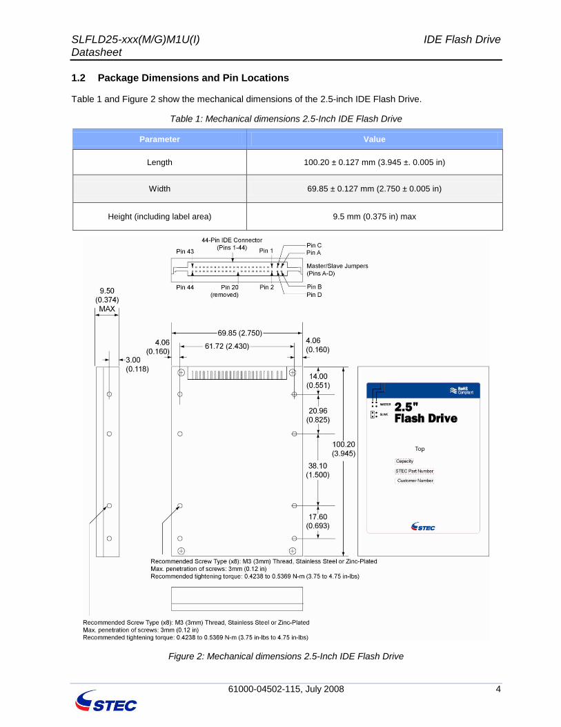
1.2 Package Dimensions and Pin Locations
Table 1 and Figure 2 show the mechanical dimensions of the 2.5-inch IDE Flash Drive.
Table 1: Mechanical dimensions 2.5-Inch IDE Flash Drive
Parameter Value
Length 100.20 ± 0.127 mm (3.945 ±. 0.005 in)
Width 69.85 ± 0.127 mm (2.750 ± 0.005 in)
Height (including label area) 9.5 mm (0.375 in) max
Figure 2: Mechanical dimensions 2.5-Inch IDE Flash Drive
SLFLD25-xxx(M/G)M1U(I) IDE Flash Drive Datasheet
61000-04502-115, July 2008 5
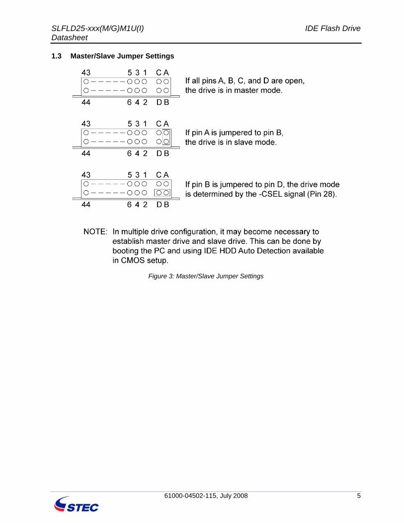
1.3 Master/Slave Jumper Settings
Figure 3: Master/Slave Jumper Settings
SLFLD25-xxx(M/G)M1U(I) IDE Flash Drive Datasheet
61000-04502-115, July 2008 6
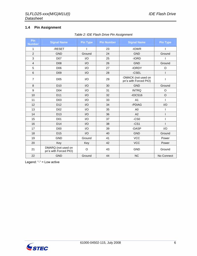
1.4 Pin Assignment
Table 2: IDE Flash Drive Pin Assignment
Pin
Number Signal Name Pin Type Pin Number Signal Name Pin Type
1 -RESET I 23 -IOWR I
2 GND Ground 24 GND Ground
3 D07 I/O 25 -IORD I
4 D08 I/O 26 GND Ground
5 D06 I/O 27 -IORDY O
6 D09 I/O 28 -CSEL I
7 D05 I/O 29 -DMACK (not used on pn’s with Forced PIO)
I
8 D10 I/O 30 GND Ground
9 D04 I/O 31 INTRQ O
10 D11 I/O 32 -IOCS16 O
11 D03 I/O 33 A1 I
12 D12 I/O 34 -PDIAG I/O
13 D02 I/O 35 A0 I
14 D13 I/O 36 A2 I
15 D01 I/O 37 -CS0 I
16 D14 I/O 38 -CS1 I
17 D00 I/O 39 -DASP I/O
18 D15 I/O 40 GND Ground
19 GND Ground 41 VCC Power
20 Key Key 42 VCC Power
21 DMARQ (not used on pn’s with Forced PIO)
O 43 GND Ground
22 GND Ground 44 NC No Connect
Legend: ―-― = Low active
SLFLD25-xxx(M/G)M1U(I) IDE Flash Drive Datasheet
61000-04502-115, July 2008 7
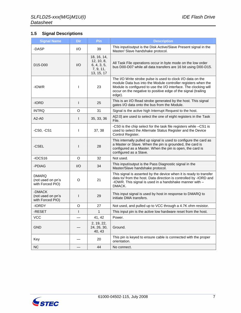
1.5 Signal Descriptions
Signal Name Dir Pin Description
-DASP I/O 39 This input/output is the Disk Active/Slave Present signal in the Master/ Slave handshake protocol.
D15-D00 I/O
18, 16, 14, 12, 10, 8, 6, 4, 3, 5, 7, 9, 11,
13, 15, 17
All Task File operations occur in byte mode on the low order bus D00-D07 while all data transfers are 16 bit using D00-D15.
-IOWR I 23
The I/O Write strobe pulse is used to clock I/O data on the module Data bus into the Module controller registers when the Module is configured to use the I/O interface. The clocking will occur on the negative to positive edge of the signal (trailing edge).
-IORD I 25 This is an I/O Read strobe generated by the host. This signal gates I/O data onto the bus from the Module.
INTRQ O 31 Signal is the active high Interrupt Request to the host.
A2-A0 I 35, 33, 36 A[2:0] are used to select the one of eight registers in the Task File.
-CS0, -CS1 I 37, 38 -CS0 is the chip select for the task file registers while –CS1 is used to select the Alternate Status Register and the Device Control Register.
-CSEL I 28
This internally pulled up signal is used to configure the card as a Master or Slave. When the pin is grounded, the card is configured as a Master. When the pin is open, the card is configured as a Slave.
-IOCS16 O 32 Not used.
-PDIAG I/O 34 This input/output is the Pass Diagnostic signal in the Master/Slave handshake protocol.
DMARQ (not used on pn’s with Forced PIO)
O 21
This signal is asserted by the device when it is ready to transfer data to/ from the host. Data direction is controlled by -IORD and -IOWR. This signal is used in a handshake manner with –DMACK.
-DMACK (not used on pn’s with Forced PIO)
I 29 This input signal is used by host in response to DMARQ to initiate DMA transfers.
-IORDY O 27 Not used, and pulled up to VCC through a 4.7K ohm resistor.
-RESET I 1 This input pin is the active low hardware reset from the host.
VCC — 41, 42 Power.
GND — 2, 19, 22,
24, 26, 30, 40, 43
Ground.
Key — 20 This pin is keyed to ensure cable is connected with the proper orientation.
NC — 44 No connect.
SLFLD25-xxx(M/G)M1U(I) IDE Flash Drive Datasheet
61000-04502-115, July 2008 8
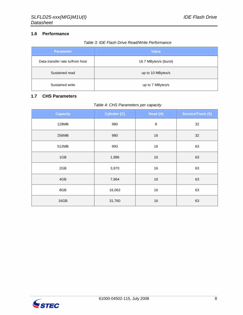
1.6 Performance
Table 3: IDE Flash Drive Read/Write Performance
Parameter Value
Data transfer rate to/from host 16.7 MBytes/s (burst)
Sustained read up to 10 MBytes/s
Sustained write up to 7 MBytes/s
1.7 CHS Parameters
Table 4: CHS Parameters per capacity
Capacity Cylinder (C) Head (H) Sectors/Track (S)
128MB 980 8 32
256MB 980 16 32
512MB 993 16 63
1GB 1,986 16 63
2GB 3,970 16 63
4GB 7,964 16 63
8GB 16,062 16 63
16GB 31,760 16 63

SLFLD25-xxx(M/G)M1U(I) IDE Flash Drive Datasheet
61000-04502-115, July 2008 9
1.8 Standards Compliance
STEC products specified in this document are compliant with Technical Committee T13, AT Attachment-5 (ATA-5) standards and are certified for compliance with these other industry standards:
UL 950
CE, and FCC Class B & D
RoHS
1.8.1 CE and FCC Class B & D
The STEC products specified in this document meet the following requirements and limits of the European Standards:
Class B requirements of the following European Standard:
EN 55022: 1998 – ―Information technology equipment – Radio disturbance characteristics – Limits and methods of measurement‖
Class D limits of the following European Standards:
EN 61000-3-2 ―Electromagnetic compatibility (EMC) Part 3-2: Limits – Limits for harmonic current emissions (equipment input current up to and including 16 A per phase)‖
EN 61000-3-3: 1995 – ―Part 3: Limits – Section 3: Limitation of voltage fluctuations and flicker in low-voltage supply systems for equipment with rated current <= 16A‖
EN 55024 – ―Information technology equipment – Immunity characteristics – Limits and methods of measurement‖
1.8.2 RoHS
STEC certifies that its products do not contain any of the restricted substances as stated below and are in compliance with RoHS EU directive 2002/95/EC, specifically:
Mercury (Hg)
Cadmium Cd)
Chromium VI (Cr +6)
Polybrominated biphenyl (PBB)
Polybrominated biphenyl ether (PBDE)
Lead (Pb)
Materials used in the STEC’s products are limited to the following:
Steel, Nylon 6/6, PCB laminate
Copper, Gold, Nickel
Silicon on ICs and Components
Polyester on Labels
SLFLD25-xxx(M/G)M1U(I) IDE Flash Drive Datasheet
61000-04502-115, July 2008 10
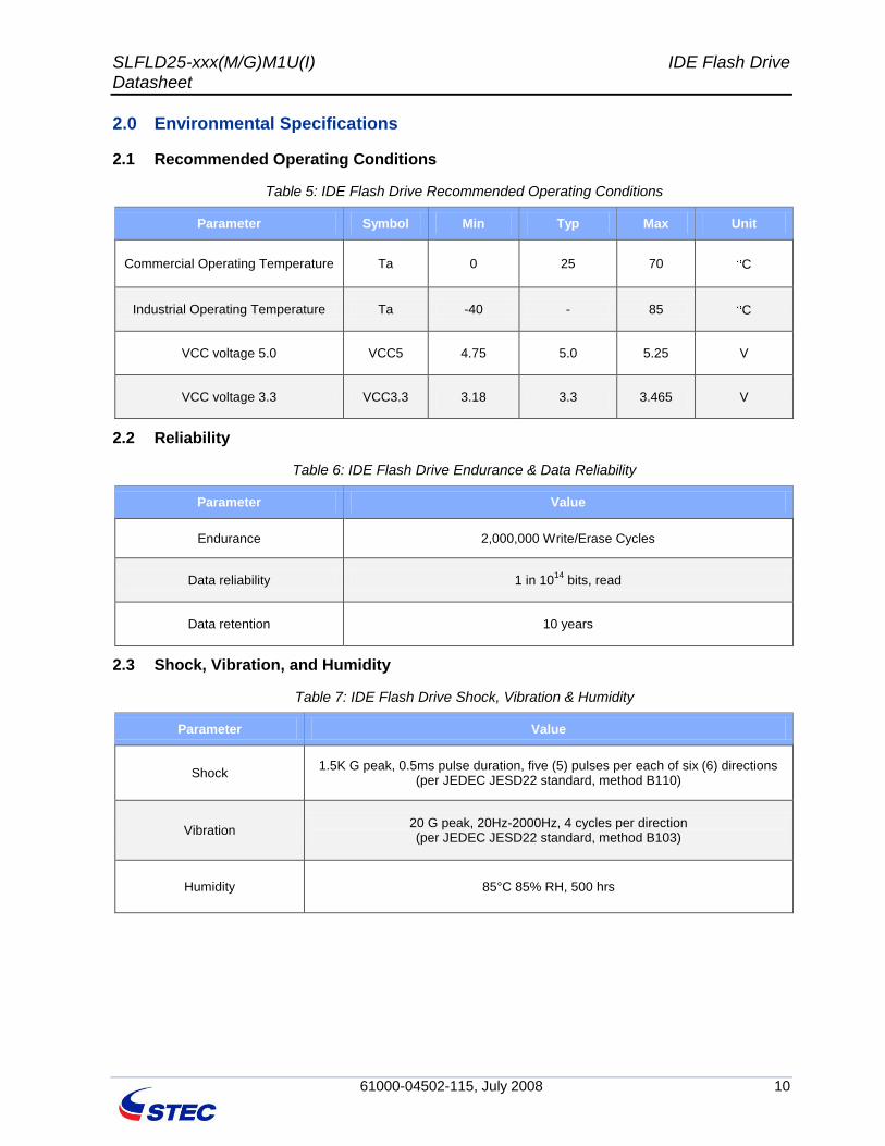
2.0 Environmental Specifications
2.1 Recommended Operating Conditions
Table 5: IDE Flash Drive Recommended Operating Conditions
Parameter Symbol Min Typ Max Unit
Commercial Operating Temperature Ta 0 25 70 C
Industrial Operating Temperature Ta -40 - 85 C
VCC voltage 5.0 VCC5 4.75 5.0 5.25 V
VCC voltage 3.3 VCC3.3 3.18 3.3 3.465 V
2.2 Reliability
Table 6: IDE Flash Drive Endurance & Data Reliability
Parameter Value
Endurance 2,000,000 Write/Erase Cycles
Data reliability 1 in 1014
bits, read
Data retention 10 years
2.3 Shock, Vibration, and Humidity
Table 7: IDE Flash Drive Shock, Vibration & Humidity
Parameter Value
Shock 1.5K G peak, 0.5ms pulse duration, five (5) pulses per each of six (6) directions
(per JEDEC JESD22 standard, method B110)
Vibration 20 G peak, 20Hz-2000Hz, 4 cycles per direction (per JEDEC JESD22 standard, method B103)
Humidity 85°C 85% RH, 500 hrs

SLFLD25-xxx(M/G)M1U(I) IDE Flash Drive Datasheet
61000-04502-115, July 2008 11
3.0 Electrical Specifications
3.1 Absolute Maximum Ratings
Table 8: IDE Flash Drive Absolute Maximum Ratings
Parameter Symbol Value Unit
Voltage Vin, Vout -0.5 to VCC +0.5 V
Storage temperature range Tstg -65 to +150 C
3.2 DC Characteristics
Measurements at Recommended Operating Conditions unless otherwise specified.
Table 9: IDE Flash Drive DC Characteristics
Symbol Parameter Min Max Unit Notes
VIL Input LOW Voltage -0.3 +0.8 V VCC=3.3V or 5.0V
VIH Input HIGH Voltage 2.0 VCC +0.3 V VCC=3.3V or 5.0V
VOL3.3 Output LOW Voltage 3.3 0.45 V VCC=3.3V
VOL5 Output LOW Voltage 5 0.8 VCC=5.0V
VOH Output HIGH Voltage 2.4 V VCC=3.3V or 5.0V
ICCSB Standby Mode 2 mA ICC at VCC=3.3V or 5.0V
ICC Operating Current 75 mA ICC at VCC=3.3V or 5.0V
Operating current measured with 2-way interleaving.
ILI Input Leakage Current 10 µA VCC=3.3V or 5.0V
ILO3.3 Output Leakage Current 3.3 1 µA VCC=3.3V
ILO5 Output Leakage Current 5 2 µA VCC= 5.0V
CI/O Input/output Capacitance 25 pF VCC=3.3V or 5.0V

SLFLD25-xxx(M/G)M1U(I) IDE Flash Drive Datasheet
61000-04502-115, July 2008 12
3.3 AC Characteristics
Measurements at Recommended Operating Conditions, unless otherwise specified.
3.3.1 True IDE Mode Register Access
Table 10: True IDE Mode Register Access AC Characteristics
Parameter Symbol Mode0 Mode1 Mode2 Mode3 Mode4 Mode5 Mode6 Unit
Cycle time (min) t0 600 383 330 180 120 100 80 ns
Address valid to -IORD/-IOWR
(min) setup t1 70 50 30 30 25 15 10 ns
-IORD/-IOWR pulse width 8bit
(min) t2 290 290 290 80 70 65 55 ns
-IORD/-IOWR recovery time
(min) t2i — — — 70 25 25 20 ns
-IOWR data setup (min)
t3 60 45 30 30 20 20 15 ns
-IOWR data hold (min)
t4 30 20 15 10 10 5 5 ns
-IORD data setup (min)
t5 50 35 20 20 20 15 10 ns
-IORD data hold (min)
t6 5 5 5 5 5 5 5 ns
-IORD data tristate (max)
t6z 30 30 30 30 30 20 20 ns
Addresses valid to -IOCS16
assert. (max) t7 90 50 40 N/A N/A N/A N/A ns
Address valid to -IOCS16
release (max) t8 60 45 30 N/A N/A N/A N/A ns
-IORD/-IOWR to address valid
hold t9 20 15 10 10 10 10 10 ns

SLFLD25-xxx(M/G)M1U(I) IDE Flash Drive Datasheet
61000-04502-115, July 2008 13
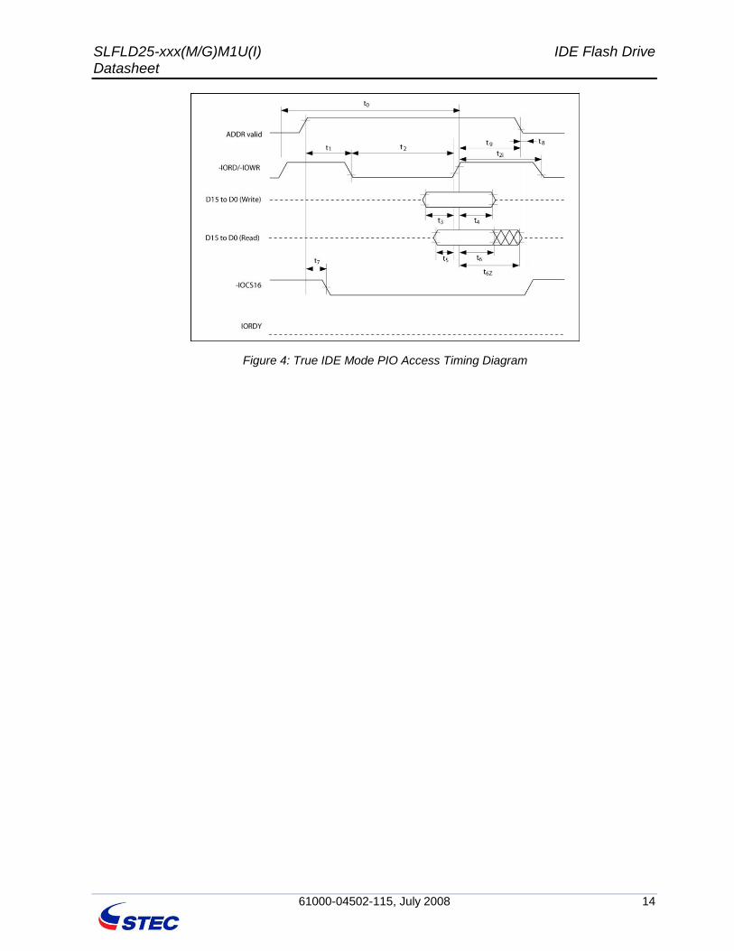
3.3.2 True IDE Mode PIO Access
Table 11: True IDE Mode PIO Access AC Characteristics
Parameter Symbol Mode0 Mode1 Mode2 Mode3 Mode4 Mode5 Mode6 Unit
Cycle time (min) t0 600 383 330 180 120 100 80 ns
Address valid to -IORD/-IOWR
(min) setup t1 70 50 30 30 25 15 10 ns
-IORD/-IOWR pulse width 8bit
(min) t2 290 290 290 80 70 65 55 ns
-IORD/-IOWR recovery time
(min) t2i — — — 70 25 25 20 ns
-IOWR data setup (min)
t3 60 45 30 30 20 20 15 ns
-IOWR data hold (min)
t4 30 20 15 10 10 5 5 ns
-IORD data setup (min)
t5 50 35 20 20 20 15 10 ns
-IORD data hold (min)
t6 5 5 5 5 5 5 5 ns
-IORD data tristate (max)
t6z 30 30 30 30 30 20 20 ns
Addresses valid to -IOCS16
assert. (max) t7 90 50 40 N/A N/A N/A N/A ns
Address valid to -IOCS16 release
t8 60 45 30 N/A N/A N/A N/A ns
-IORD/-IOWR to address valid
hold t9 20 15 10 10 10 10 10 ns
SLFLD25-xxx(M/G)M1U(I) IDE Flash Drive Datasheet
61000-04502-115, July 2008 14
Figure 4: True IDE Mode PIO Access Timing Diagram

SLFLD25-xxx(M/G)M1U(I) IDE Flash Drive Datasheet
61000-04502-115, July 2008 15
3.3.3 True IDE Mode Multiword DMA (not used on pn’s with Forced PIO)
Table 12: True IDE Mode Multiword DMA AC Characteristics
Parameter Symbol Mode 0 Mode 1 Mode 2 Mode 3 Mode 4 Unit
Cycle time (min) t0 480 150 120 100 80 ns
-IORD/-IOWR Asserted Pulse (min)
tD 215 80 70 65 55 ns
-IORD data access (max) tE 150 60 50 50 45 ns
-IORD data hold (min) tF 5 5 5 5 5 ns
-IORD/-IOWR data setup (min)
tG 100 30 20 15 10 ns
-IOWR data hold (min) tH 20 15 10 5 5 ns
DMACK to -IORD/-IOWR setup (min)
tI 0 0 0 0 0 ns
-IORD/-IOWR to DMACK hold (min)
tJ 20 5 5 5 5 ns
-IORD negated pulse width (max)
tKR 50 50 25 25 20 ns
-IOWR negated pulse width (min)
tKW 215 50 25 25 20 ns
-IORD to DMARQ delay (max) tLR 120 40 35 35 35 ns
-IOWR to DMARQ delay (max)
tLW 40 40 35 35 35 ns
Figure 5: True IDE Mode Multiword DMA Timing Diagram

SLFLD25-xxx(M/G)M1U(I) IDE Flash Drive Datasheet
61000-04502-115, July 2008 16
4.0 Identify Drive Parameter Information
An example of the parameter information received from the IDE Flash Drive when invoking the Identify Drive command (ECh) is listed in Table 13.
Table 13: Identify Drive Parameter Information
Word
Address Data
Total
Bytes Description
0 044AH 2 Value fixed by CFA
1 XXXXH 2 Default number of cylinders
2 0000H 2 Reserved
3 00XXH 2 Default number of heads
4 XXXXH 2 Do not use this word. Before retirement, was number of unformatted bytes per track
5 XXXXH 2 Do not use this word. Before retirement, was number of unformatted bytes per sector
6 XXXXH 2 Default number of sectors per track
7 - 8 XXXXH 4 Number of sectors per IDE Flash Drive (word 7 = MSW, word 8 = LSW)
9 0000H 2 Reserved
10 - 19 Unique per card 20 Serial Number in ASCII (20 characters): STEC proprietary
20 XXXXH 2 Do not use this word. Before retirement, was buffer type
21 XXXXH 2 Do not use this word. Before retirement, was buffer size in 512 byte increments
22 0004H 2 # of ECC bytes passed on Read/Write Long commands
23 - 26 See description 8 Firmware revision in ASCII (8 characters): Rev8.0.0 52 65 76 38 2E 30 2E 30 hex
27 - 46 See description 40 Model Number in ASCII (40 characters): STI Flash 8.0.0 <left justified> 53 54 49 20 46 6C 61 73 68 20 38 2E 30 2E 30 20 20 20 20 20 20 20 20 20 20 20 20 20 20 20 20 20 20 20 20 20 20 20 20 20 hex
47 0001H 2 Maximum of 1 sector on Read/Write Multiple command
48 0000H 2 Double Word not supported
49 0300H 2 DMA supported, LBA supported (0200H DMA not supported, LBA supported for pn’s with Forced PIO)
50 0000H 2 Reserved
51 0200H 2 PIO data transfer cycle timing mode
52 0000H 2 Single word DMA data transfer cycle timing mode (not supported)
53 0003h 2 Words 54 - 58 and 64 - 70 are valid
54 XXXXH 2 Number of Current Cylinders
55 XXXXH 2 Number of Current Heads
56 XXXXH 2 Number of Current Sectors Per Track
57 XXXXH 2 LSW of the Current Capacity in Sectors
58 XXXXH 2 MSW of the Current Capacity in Sectors
59 010XH 2 Current Setting for Block Count=1 for R/W Multiple commands
60 - 61 XXXXH 4 Total number of sectors addressable in LBA Mode
62 0000H 2 Single word DMA transfer not supported
63 0407H 2 Multiword DMA modes supported (0000H MWDMA modes not supported for pn’s with Forced PIO)
64 0003H 2 Advanced PIO modes supported (modes 3 and 4)
65 0078H 2 Minimum multiword DMA transfer cycle time per word (ns) (0000H for pn’s with Forced PIO)
66 0078H 2 Recommended multiword DMA transfer cycle time per word (ns) (0000H MWDMA pn’s with Forced PIO)
67 0078H 2 Minimum PIO transfer without flow control
68 0078H 2 Minimum PIO transfer with IORDY flow control
69 - 255 0000H 374 Reserved
XXXXH = These values depend on the specific IDE Flash Drive.

SLFLD25-xxx(M/G)M1U(I) IDE Flash Drive Datasheet
61000-04502-115, July 2008 17
5.0 Registers
This chapter lists the registers of the IDE Flash Drive. Refer to ATA/IDE standards for further details, including Task File Register mapping and bit definitions of each Task File Register.
The Data Register is accessed in word (16-bit) mode at power up. The IDE Flash Drive permits 8-bit accesses if the host issues a Set Feature Command to put the IDE Flash Drive in 8-bit mode.
Table 14: IDE Flash Drive Task File Registers
Task File Register Description
Data Register The Data Register is a 16-bit read/write register used for transferring data between the IDE Flash Drive and the host. This register can be accessed in word mode and byte mode.
Error Register
The Error Register is a read-only register that is used for analyzing an error. This register is valid when the BSY bit in the Status register and Alternate Status register are set to ―0‖ (Ready). Diagnostic Codes are returned in the Error Register after a Execute Drive Diagnostic command (code 90h). Extended Error Codes returned in the Error Register after a Request Sense command (code 03h).
Sector Count Register This register contains the numbers of sectors of data requested to be transferred on a read or write operation between the host and the IDE Flash Drive. If the value in the register is 0, a count of 256 sectors is indicated.
Sector Number Register When the LBA bit in the Drive/Head register is 0, this register contains the starting sector number for any media access. When the LBA bit is set to 1, this register contains bits 7:0 of the LBA for any media access.
Cylinder Low Register In CHS mode (LBA=0), this register contains the low-order bits of the starting cylinder address. In LBA mode, it contains bits 15:8 of the LBA.
Cylinder High Register In CHS mode (LBA=0), this register contains the high-order bits of the starting cylinder address. In LBA mode, it contains bits 23:16 of the LBA.
Drive/Head Register This register selects the IDE Flash Drive address translation (CHS or LBA) and provides head address (CHS) or high-order address bits 27:24 for LBA.
Status Register This read-only register indicates status of a command execution. When the BSY bit is ―0‖, the other bits are valid; when the BSY bit is ―1‖, the other bits are not valid. When the register is read, the interrupt pin, is cleared.
Alternate Status Register This register is the same as the Status register, except that is not negated when the register is read.
Device Control Register This write-only register is used for controlling the interrupt request and issuing an ATA soft reset to the IDE Flash Drive.
Drive Address Register
This read-only register is used for confirming the IDE Flash Drive’s status. This register is provided for compatibility with the AT disk drive interface and it is not recommended that this register be mapped into the host’s I/O space because of potential conflicts on bit 7.
Command Register
This write-only register is used for writing the command that executes the IDE Flash Drive’s operation. The command code is written in the command register after its parameters are written in the Task File during the IDE Flash Drive ready state.
SLFLD25-xxx(M/G)M1U(I) IDE Flash Drive Datasheet
61000-04502-115, July 2008 18
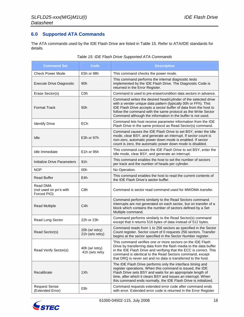
6.0 Supported ATA Commands
The ATA commands used by the IDE Flash Drive are listed in Table 15. Refer to ATA/IDE standards for details.
Table 15: IDE Flash Drive Supported ATA Commands
Command Set Code Description
Check Power Mode E5h or 98h This command checks the power mode.
Execute Drive Diagnostic 90h This command performs the internal diagnostic tests implemented by the IDE Flash Drive. The Diagnostic Code is returned in the Error Register.
Erase Sector(s) C0h Command is used to pre-erase/condition data sectors in advance.
Format Track 50h
Command writes the desired head/cylinder of the selected drive with a vender unique data pattern (typically 00h or FFh). This IDE Flash Drive accepts a sector buffer of data from the host to follow the command with the same protocol as the Write Sector Command although the information in the buffer is not used.
Identify Drive ECh Command lets host receive parameter information from the IDE Flash Drive in the same protocol as Read Sector(s) command.
Idle E3h or 97h
Command causes the IDE Flash Drive to set BSY, enter the Idle mode, clear BSY, and generate an interrupt. If sector count is non-zero, automatic power down mode is enabled. If sector count is zero, the automatic power down mode is disabled.
Idle Immediate E1h or 95h This command causes the IDE Flash Drive to set BSY, enter the Idle mode, clear BSY, and generate an interrupt.
Initialize Drive Parameters 91h This command enables the host to set the number of sectors per track and the number of heads per cylinder.
NOP 00h No Operation.
Read Buffer E4h This command enables the host to read the current contents of the IDE Flash Drive’s sector buffer.
Read DMA (not used on pn’s with Forced PIO)
C8h Command is sector read command used for MWDMA transfer.
Read Multiple C4h
Command performs similarly to the Read Sectors command. Interrupts are not generated on each sector, but on transfer of a block which contains the number of sectors defined by a Set Multiple command.
Read Long Sector 22h or 23h Command performs similarly to the Read Sector(s) command except that it returns 516 bytes of data instead of 512 bytes.
Read Sector(s) 20h (w/ retry) 21h (w/o retry)
Command reads from 1 to 256 sectors as specified in the Sector Count register. Sector count of 0 requests 256 sectors. Transfer begins at the sector specified in the Sector Number register.
Read Verify Sector(s) 40h (w/ retry) 41h (w/o retry
This command verifies one or more sectors on the IDE Flash Drive by transferring data from the flash media to the data buffer in the IDE Flash Drive and verifying that the ECC is correct. This command is identical to the Read Sectors command, except that DRQ is never set and no data is transferred to the host.
Recalibrate 1Xh
The IDE Flash Drive performs only the interface timing and register operations. When this command is issued, the IDE Flash Drive sets BSY and waits for an appropriate length of time, after which it clears BSY and issues an interrupt. When this command ends normally, the IDE Flash Drive is initialized.
Request Sense (Extended Error)
03h Command requests extended error code after command ends with error. Extended error code is returned in the Error Register
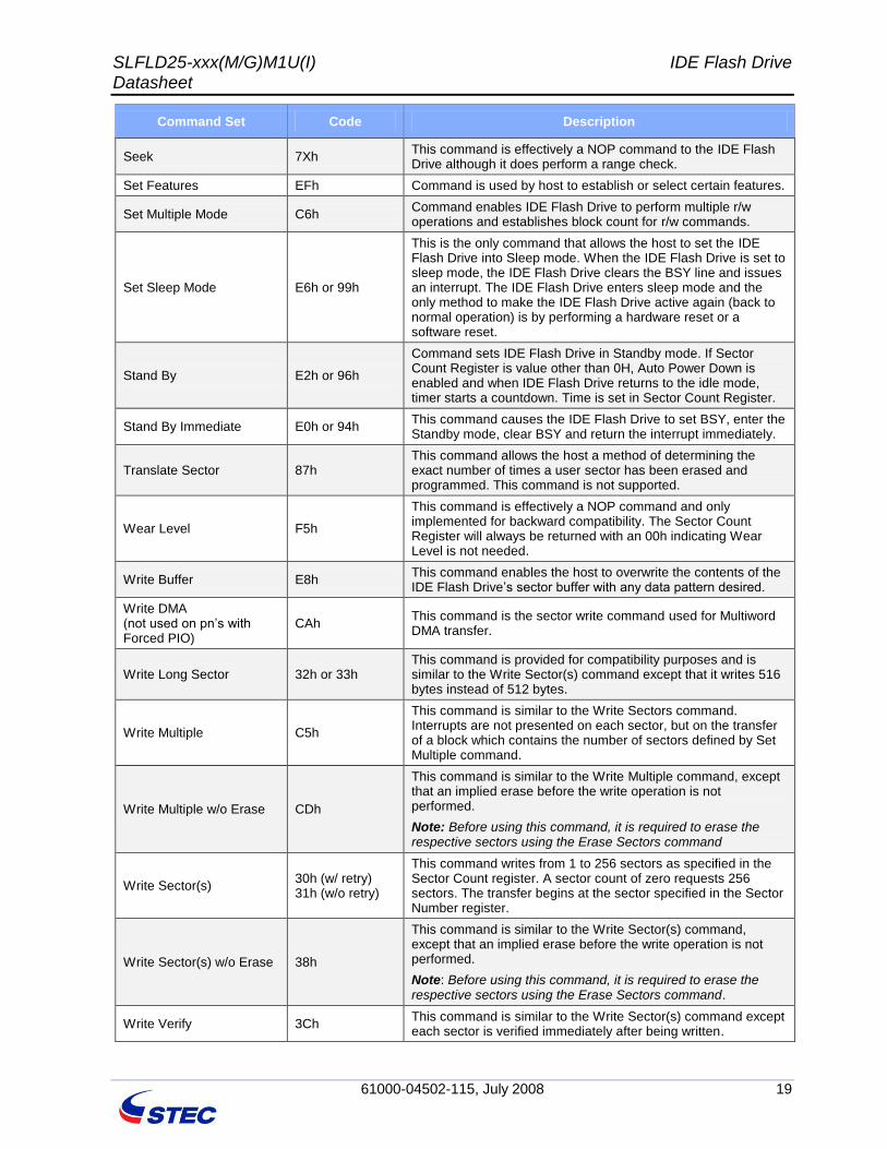
SLFLD25-xxx(M/G)M1U(I) IDE Flash Drive Datasheet
61000-04502-115, July 2008 19
Command Set Code Description
Seek 7Xh This command is effectively a NOP command to the IDE Flash Drive although it does perform a range check.
Set Features EFh Command is used by host to establish or select certain features.
Set Multiple Mode C6h Command enables IDE Flash Drive to perform multiple r/w operations and establishes block count for r/w commands.
Set Sleep Mode E6h or 99h
This is the only command that allows the host to set the IDE Flash Drive into Sleep mode. When the IDE Flash Drive is set to sleep mode, the IDE Flash Drive clears the BSY line and issues an interrupt. The IDE Flash Drive enters sleep mode and the only method to make the IDE Flash Drive active again (back to normal operation) is by performing a hardware reset or a software reset.
Stand By E2h or 96h
Command sets IDE Flash Drive in Standby mode. If Sector Count Register is value other than 0H, Auto Power Down is enabled and when IDE Flash Drive returns to the idle mode, timer starts a countdown. Time is set in Sector Count Register.
Stand By Immediate E0h or 94h This command causes the IDE Flash Drive to set BSY, enter the Standby mode, clear BSY and return the interrupt immediately.
Translate Sector 87h This command allows the host a method of determining the exact number of times a user sector has been erased and programmed. This command is not supported.
Wear Level F5h
This command is effectively a NOP command and only implemented for backward compatibility. The Sector Count Register will always be returned with an 00h indicating Wear Level is not needed.
Write Buffer E8h This command enables the host to overwrite the contents of the IDE Flash Drive’s sector buffer with any data pattern desired.
Write DMA (not used on pn’s with Forced PIO)
CAh This command is the sector write command used for Multiword DMA transfer.
Write Long Sector 32h or 33h This command is provided for compatibility purposes and is similar to the Write Sector(s) command except that it writes 516 bytes instead of 512 bytes.
Write Multiple C5h
This command is similar to the Write Sectors command. Interrupts are not presented on each sector, but on the transfer of a block which contains the number of sectors defined by Set Multiple command.
Write Multiple w/o Erase CDh
This command is similar to the Write Multiple command, except that an implied erase before the write operation is not performed.
Note: Before using this command, it is required to erase the respective sectors using the Erase Sectors command
Write Sector(s) 30h (w/ retry) 31h (w/o retry)
This command writes from 1 to 256 sectors as specified in the Sector Count register. A sector count of zero requests 256 sectors. The transfer begins at the sector specified in the Sector Number register.
Write Sector(s) w/o Erase 38h
This command is similar to the Write Sector(s) command, except that an implied erase before the write operation is not performed.
Note: Before using this command, it is required to erase the respective sectors using the Erase Sectors command.
Write Verify 3Ch This command is similar to the Write Sector(s) command except each sector is verified immediately after being written.
SLFLD25-xxx(M/G)M1U(I) IDE Flash Drive Datasheet
61000-04502-115, July 2008 20
7.0 Revision History
Revision Date Description
-101 11/20/06 Product release.
-102 12/14/06 ID file Serial Number, Firmware Revision, and Model Number corrected in table.
-103 1/16/07 Logo updated. Disclaimer updated. Contact Information added.
-104 2/23/07 In between capacities removed from Ordering Information and CHS parameters. Serial number revision (paper correction only).
-105 2/28/07 CSEL signal description corrected. 16GB CHS parameters added. DC Characteristics corrected
-106 4/10/07 Shock updated from 1K to 1.5K. Vibration updated from 15 to 20.
-107 5/21/07. Label seciton added.
-108 6/11/07 Connector location added to label section. Label added to dimension illustration.
-109 8/06/07 Warranty bullet removed from features column on page 1
-110 9/19/07 General Description text updated.
-111 11/12/07 Layout updated for consistency and easier editing. Disclaimer notice reformatted with headings.
-112 3/7/08 Contact information on last page updated.
-113 4/2/08 STEC China address on last page updated.
-114 5/29/08 P designator added to Ordering Information.
-115 7/17/08 Recommended torque for screw on dimension illustration corrected from 6.0 in-lbs to 3.75-4.75 in-lbs.
SLFLD25-xxx(M/G)M1U(I) IDE Flash Drive Datasheet
61000-04502-115, July 2008 21
DISCLAIMER OF LIABILITY
STEC™ Inc. reserves the right to make changes to specifications and product descriptions such as but not limited to numbers, parameters and other technical information contained herein without notice. Please contact the STEC™ Inc. sales office to obtain the latest specifications. STEC™ Inc. grants no warranty with respect to this datasheet, neither explicit or implied, and is not liable for direct or indirect damages. Some states do not grant the exclusion of incidental damages and as such this statement may not be valid in such states. The provisions of the datasheet do not convey to the purchaser of the device any license under any patent rights or other intellectual property rights of STEC Inc. or others.
EXPORT ADMINISTRATION REGULATIONS
The information provided may be subject to United States Export Controls. Such information should not be downloaded or exported (i), into (or to a national or resident of) Cuba, Iraq, Libya, North Korea, Iran, Syria, or any other country to which the United States has embargoed goods; or given to (ii), anyone on the United States Treasury Department’s list of Specially Designated Nationals or the U.S. Commerce Departments’s Table of Deny Orders. By using the information, you represent and warrant that you are not located in, under the control of, or a national or resident of any such country or on any such list.
COPYRIGHT NOTICE
Copyright © 2007 by STEC™ Inc. All rights reserved. Information contained in this document, including but not limited to any instructions, descriptions and product specifications, is considered proprietary and confidential to STEC™, Inc. and shall not be modified, used, copied, reproduced or disclosed in whole or in part, in any form or by any means, electronic or mechanical, for any purpose, without the written consent of STEC™ Inc
Worldwide Headquarters
STEC, Inc. 3001 Daimler Street Santa Ana, California 92705 USA Tel: (949) 476-1180 Fax: (949) 476-1209 www.stec-inc.com/
STEC Europe
Donau-City-Strasse 1 1220 Vienna, Austria Tel: +43 1 263 38 08 Fax: +43 1 263 37 65 www.stec-inc.com/
STEC Japan
Arents Daikanyama 114 11-1 Hachiyama-cho Shibuya-ku, Tokyo 150-0035 Japan Tel: +81(0) 3-5428-2231 Tel: +81(0) 3-5489-0230 www.stec-inc.jp/
STEC Malaysia
STEC Techology Sdn Bhd Plot 107 Bayan Lepas Industrial Park Phase 4, 11900 Penang, Malaysia Tel: +60 (4)-6198888 www.stec-inc.com/
STEC China
RM1805, 18F Bund Centre 222 Yan An Rd East HuangPu District Shanghai, 200002. P R. China Tel: +86 21 6132 3892 * 629 Fax: +86 21 6335 1336 www.stecchina.cn/


![CR-1 : @TAWAS B LIB.TAWAS B(SCH 1):PAGE1 TAWASnotebookschematic.org/data/NOTEBOOK/attachments/SC... · resume gp[6] gp[7] gp[8] gp[9] 3.3v 3.3v 3.3v 3.3v gp[23] gp[24] gp[25] gp[26]](https://img.pdfslide.us/doc/110x75/5f812ff679030c23f20de0bd/cr-1-tawas-b-libtawas-bsch-1page1-ta-resume-gp6-gp7-gp8-gp9-33v.jpg)

![CONTENTS · Each LED is driven directly by ... PIN_F3 LED Green[5] 3.3V LED[6] PIN_B1 LED Green[6] 3.3V LED[7] PIN_L3 LED Green[7] 3.3V . …](https://img.pdfslide.us/doc/110x75/5b5b57cd7f8b9a55388e240b/contents-each-led-is-driven-directly-by-pinf3-led-green5-33v-led6.jpg)