Embed Size (px)
Citation preview
INDUCTIVELY COUPLED PLASMA ETCHING ON GaN
By
SITI AZLINA BINTI ROSLI
Thesis submitted in fulfillment of the requirements for the degree of Master of Science
January 2010
ACKNOWLEDGEMENTS
Firstly, I would like to express my deepest gratitude to my supervisor, Associate
Prof. Dr Azlan Abdul Aziz, for his guidance and support throughout the course of
my research. He has been more than helpful in creating opportunities for priceless
learning experience during his supervision. I also admire his patience with my pace
of work. I also would like to sincerely thank Associate Prof. Dr. Roslan, for
additional advice and help. Without his patience, guidance and constant supports,
this work would not have been possible.
Secondly, my sincere thanks go to Mrs. Ee Bee Choo, Mr. Jamil, Mr. Hazhar and
Mr. Mokhtar for their generous help and technical support offered during my
laboratorial work. Their patience when working with me during my experiments is
truly appreciated as my work can be very repetitive and unexciting from others point
of view. I would also like to thank my research colleagues, especially Dr Maghdy,
Ms Mazlindawati and my entire colleague especially at N.O.R lab for their assistance
in research, ingenious ideas during discussion and lasting friendship together.
Last but most importantly, I wish to acknowledge the care and encouragement given
by my loving parents and my siblings. Thank you very much for supporting me in so
many ways from the beginning until the end.
11
TABLE OF CONTENTS
Page
ACKNOWLEDGEMENTS 11
TABLE OF CONTENTS l1l
LIST OF TABLES Vll
LIST OF FIGURES Vlll
LIST OF SYMBOLS xii
LIST OF ABBREVIATION XlV
ABSTRAK xvi
ABSTRACT XVlll
CHAPTER 1 : INTRODUCTION 1
1.1 Introduction 1
1.2 III- V Nitrides for Device Applications 1
1.2.1 Gallium Nitrides 4
1.2.2 Lack of suitable etchants 5
1.2.3 Dry Etching 6
1.3 Research Objectives 8
1.4 Outline of the thesis 9
CHAPTER 2 : THEORY OF PLASMA ETCHING 10
2.1 Introduction 10
2.2 Etching 10
2.3 Wet Etching 11
2.3.1 General Principles of Wet Etching 11
2.4 Dry Etching 12
2.4.1 Dry Processing 12
2.4.2 Plasma Fundamentals 13
2.4.3 Paschen Law 15
2.4.4 The formation of a DC voltage 16
lll
2.4.5 Influence of DC Bias 19
2.4.5.1 Influence ofthe dimensions of the reactor and 19 etching mode
2.4.5.2 Influence of the plasma parameters 20
2.4.5.2.1 Gases and Flow 20
2.4.5.2.2 Pressure 21
2.4.5.2.3 Power 22
2.4.6 Sheath Formation 22
2.4.7 Potential Distribution 24
2.4.8 Mechanisms of Dry Etching 26
2.5 Dry Etching Technique 29
2.5.1 Plasma Etching (PE) 31
2.5.2 Reactive Ion Etching (RIE) 32
2.5.3 Inductively Coupled Plasma Etching (ICP) 34
2.5.3.1 Anisotropic 39
2.5.4 Literature review of chlorine based plasma etching on 41 GaN.
2.5.4.1 Chlorine based- dry etching 42
CHAPTER3: INSTRUMENTATIONS 48
3.1 Introduction 48
3.2 Film Thickness Measurements 48
3.2.1 Filmetrics 48
3.3 Physical microscopy 49
3.3.1 Scanning Electron Microscopy (SEM) 49
3.3.2 Atomic Force Microscopy (AFM) 52
3.4 Plasmalab 80Plus ICP-RIE System 53
3.5 Physical metal deposition 55
3.5.1 Thermal evaporator 55
IV
CHAPTER 4: FABRICATION
4.1 Introduction
4.2 Wafer cleaning and native oxide removal
4.3 Mask design
4.3.1 Linear and square mask fabrication
4.3.2 Optical lithography
4.3.2.1 Procedures ofthe optical lithography process
4.3.3 Procedures of the Electron Beam Lithography
4.4 Metallization utilizing thermal evaporator
4.4.1 Film Thickness
4.5 Lift-off process
4.6 Summary of the fabrication flow
CHAPTER 5: STUDY OF THE EFFECTS OF Clz/Ar On GaN
ETCHING
5.1 Introduction
5.2 Effects of mixtures of Argon
5.3 AFM results
5.4 SEM results
5.5 Effects of pressure
5.6 Effects of ICP power
5.7 Pattern of cross section observation for GaN using Electron Beam Lithography
CHAPTER 6 : STUDY OF THE EFFECTS OF Clz/H2 On GaN
ETCIDNG
6.1 Introduction
6.2 Effects of mixtures ofHydrogen
6.3 AFM results
6.4 SEM results
v
58
58
58
59
59
61
61
64
65
66
66
67
70
70
70
73
76
78
81
84
86
86
86
89
91
6.5 Effects of pressure
6.6 Effects of ICP power
6. 7 Comparison of additive gases of Ar and H2 into Ch
CHAPTER 7 : CONCLUSIONS AND FUTURE WORKS
REFERENCE
PUBLICATION AND SEMINARS
APPENDICES
94
97
99
101
104
110
Appendix A The location of major component in 80Plus Plasmalab 112 ICP-RIE machine
Appendix B Physical Properties ofNickel (Ni) 114
Vl
LIST OF TABLE
Table 1.1 Comparison of300 K semiconductor material 3
properties. (Adapted from Sawin, 1985).
Table 2.1 The distinctions between the two rate limiting steps. 11
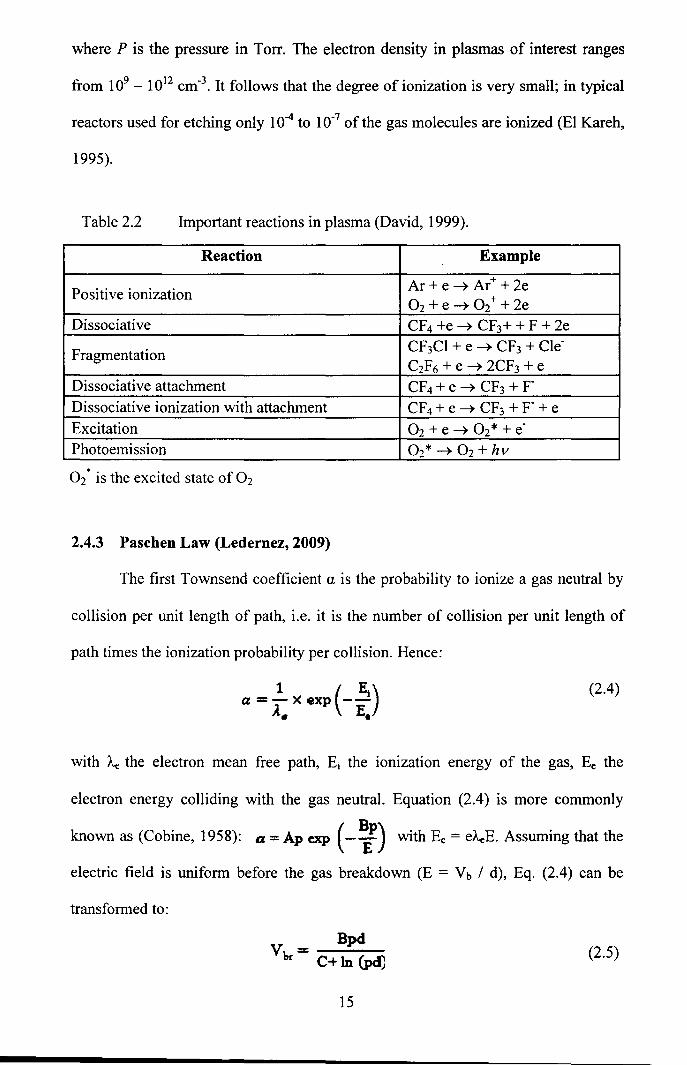
Table 2.2 Important reactions in plasma (David, 1999). 15
Table 2.3 Boiling points for possible etches products oflll-V 41
nitrides etched in halogen- or CH.JH2-based plasmas. (Adapted from Pearton, 2000)
Table 2.4 Summary of etch rate results for GaN with different 47
plasma chemistries in ICP technique (Rosli et al.
(2005).
Table 4.1 The properties of Gallium Nitrides (GaN) 57
Table 4.2 Thickness ofNi fabricated on GaN 65
Table 4.3 Flow of pattern transfer from the mask to the wafer 67
Table 4.4 Description of the order in fabrication process 68
Table 6.1 Gas for GaN and trench etching with their main 86
plasma radicals and products.
Vll
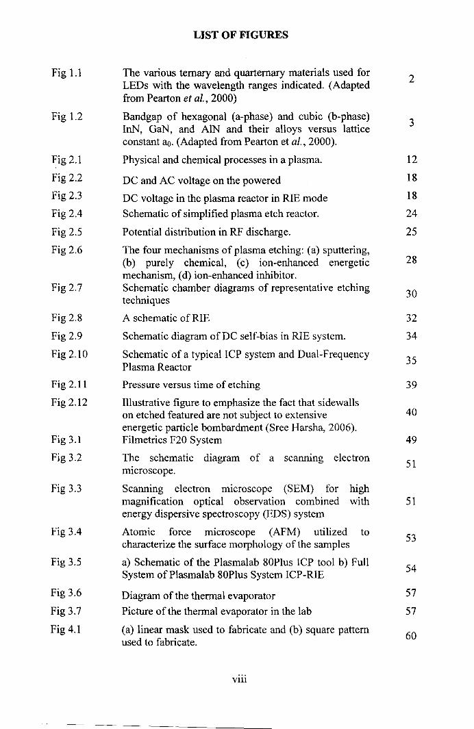
Fig 1.1
Fig 1.2
Fig 2.1
Fig 2.2
Fig 2.3
Fig 2.4
Fig 2.5
Fig 2.6
Fig 2.7
Fig 2.8
Fig 2.9
Fig 2.10
Fig 2.11
Fig 2.12
Fig 3.1
Fig 3.2
Fig 3.3
Fig 3.4
Fig 3.5
Fig 3.6
Fig 3.7
Fig 4.1
LIST OF FIGURES
The various ternary and quarternary materials used for LEDs with the wavelength ranges indicated. (Adapted from Pearton et al., 2000)
Bandgap of hexagonal (a-phase) and cubic (b-phase) InN, GaN, and AlN and their alloys versus lattice constant ao. (Adapted from Pearton et al., 2000).
Physical and chemical processes in a plasma.
DC and AC voltage on the powered
DC voltage in the plasma reactor in RIE mode
Schematic of simplified plasma etch reactor.
Potential distribution in RF discharge.
The four mechanisms of plasma etching: (a) sputtering, (b) purely chemical, (c) ion-enhanced energetic mechanism, (d) ion-enhanced inhibitor. Schematic chamber diagrams of representative etching techniques
A schematic of RIE
Schematic diagram of DC self-bias in RIE system.
Schematic of a typical ICP system and Dual-Frequency Plasma Reactor
Pressure versus time of etching
Illustrative figure to emphasize the fact that sidewalls on etched featured are not subject to extensive energetic particle bombardment (Sree Harsha, 2006). Filmetrics F20 System
The schematic diagram of a scanning electron microscope.
Scanning electron microscope (SEM) for high magnification optical observation combined with energy dispersive spectroscopy (EDS) system
Atomic force microscope (AFM) utilized to characterize the surface morphology of the samples
a) Schematic of the Plasmalab 80Plus ICP tool b) Full System ofPlasmalab 80Plus System ICP-RIE
Diagram of the thermal evaporator
Picture of the thermal evaporator in the lab
(a) linear mask used to fabricate and (b) square pattern used to fabricate.
Vlll
2
3
12
18
18
24
25
28
30
32
34
35
39
40
49
51
51
53
54
57
57
60
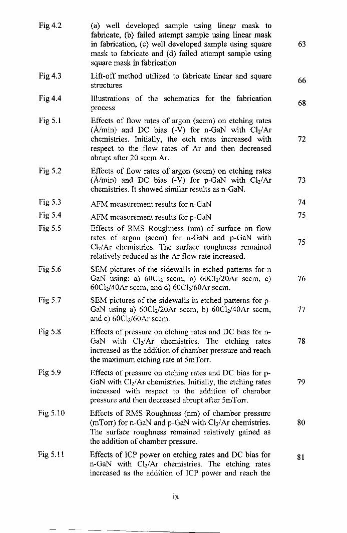
Fig 4.2
Fig 4.3
Fig 4.4
Fig 5.1
Fig 5.2
Fig 5.3
Fig 5.4
Fig 5.5
Fig 5.6
Fig 5.7
Fig 5.8
Fig 5.9
Fig 5.10
Fig 5.11
(a) well developed sample using linear mask to fabricate, (b) failed attempt sample using linear mask in fabrication, (c) well developed sample using square mask to fabricate and (d) failed attempt sample using square mask in fabrication
Lift-off method utilized to fabricate linear and square structures
Illustrations of the schematics for the fabrication process
Effects of flow rates of argon (seem) on etching rates (A/min) and DC bias (-V) for n-GaN with C}z/Ar chemistries. Initially, the etch rates increased with respect to the flow rates of Ar and then decreased abrupt after 20 seem Ar.
Effects of flow rates of argon (seem) on etching rates (A/min) and DC bias (-V) for p-GaN with C}z/Ar chemistries. It showed similar results as n-GaN.
AFM measurement results for n-GaN
AFM measurement results for p-GaN
Effects of RMS Roughness (nm) of surface on flow rates of argon (seem) for n-GaN and p-GaN with Chi Ar chemistries. The surface roughness remained relatively reduced as the Ar flow rate increased.
SEM pictures of the sidewalls in etched patterns for n GaN using: a) 60Ch seem, b) 60Ch/20Ar seem, c) 60Ch/40Ar seem, and d) 60C}z/60Ar seem.
SEM pictures of the sidewalls in etched patterns for pGaN using a) 60Ch/20Ar seem, b) 60C}z/40Ar seem, and c) 60Ch/60Ar seem.
Effects of pressure on etching rates and DC bias for nGaN with Ch/ Ar chemistries. The etching rates increased as the addition of chamber pressure and reach the maximum etching rate at 5mTorr.
Effects of pressure on etching rates and DC bias for pGaN with C}z/Ar chemistries. Initially, the etching rates increased with respect to the addition of chamber pressure and then decreased abrupt after 5mTorr.
Effects of RMS Roughness (nm) of chamber pressure (mTorr) for n-GaN and p-GaN with Ch/Ar chemistries. The surface roughness remained relatively gained as the addition of chamber pressure.
Effects of ICP power on etching rates and DC bias for n-GaN with C}z/ Ar chemistries. The etching rates increased as the addition of ICP power and reach the
IX
63
66
68
72
73
74
75
75
76
77
78
79
80
81
maximum etching rate at 200W.
Fig 5.12 Effects of ICP power on etching rates and DC bias for p-GaN with Ch/ Ar chemistries. The etching rates
82 increased as the addition of ICP power and reach the maximum etching rate at 200W. This result was same as n-GaN.
Fig 5.13 Effects of RMS Roughness (nm) of ICP power (W) for n-GaN and p-GaN with Ch/ Ar chemistries. The surface 83 roughness remained relatively gained as the addition of ICP power.
Fig 5.14 SEM pictures of the sidewalls in etched patterns for n-85
GaN using 60Ch/20Ar seem, a) and b) size of the pattern, and c) and d) smooth sidewalls and anisotropy.
Fig 6.1 Effects of n-GaN etch rates (Aimin) and DC bias (-V) as a function of flow rates of H2 (seem). The etch rate 87 gain steadily with increased flow rates of H2 and slightly decreased after 15 seem H2.
Fig 6.2 Effects of p-GaN etch rates (A/min) and DC bias (-V) 88
versus flow rates of H2 (seem). The etch rate decreased abruptly after 15 seem H2.
Fig 6.3 AFM measurement results for n-GaN 89
Fig 6.4 AFM measurement results for p-GaN 90
Fig 6.5 Flow Rates of H2 (seem) versus RMS roughness (nm). The rms roughness for n-GaN etched decreased as the 90 flow rates of H2 increased and this result was similar to p-GaN.
Fig 6.6 SEM pictures of the sidewalls in etched patterns for n 92
GaN using: a) 30Ch seem, b) 30Cb/15H2 seem, and c) 30Ch /30H2 seem.
Fig 6.7 SEM pictures of the sidewalls in etched patterns for p-93
GaN using; a) 30Ch/10H2 seem, b) 30Ch/15H2 seem and c) 30Ch/30H2 seem
Fig 6.8 Effects of chamber pressure (mTorr) versus etching 94
rates (Aimin) for n-GaN. The etching rates for n-GaN decreased as the pressure increased.
Fig 6.9 Effects of chamber pressure (mTorr) versus etching rates (Aimin). The etching rates for p-GaN decreased 95 as the pressure increased and this result was similar to n-GaN.
Fig 6.10 Effects of chamber pressure (mTorr) versus RMS roughness (nm). The rms roughness for n-GaN etched 96 increased as the chamber pressure increased and this result was similar to p-GaN.
X
Fig 6.11
Fig 6.12
Fig 6.13
Fig 6.14
Effects of ICP power on etching rates and DC bias for n-GaN with Ch/H2 chemistries. The etching rates increased as the addition of ICP power and reach the maximum etching rate at 200W. Effects of ICP power on etching rates and DC bias for p-GaN with Ch/H2 chemistries. The etching rates increased as the addition of ICP power and reach the maximum etching rate at 200W. This result was same as n-GaN. Effects of ICP power (W) versus RMS roughness (nm). The rms roughness for n-GaN etched gained as the ICP power increased and this result was similar to p-GaN. Effects of additives gases of Ch chemistries flow rates (Ar and H2) versus etch rates and roughness, respectively.
XI
97
98
99
100
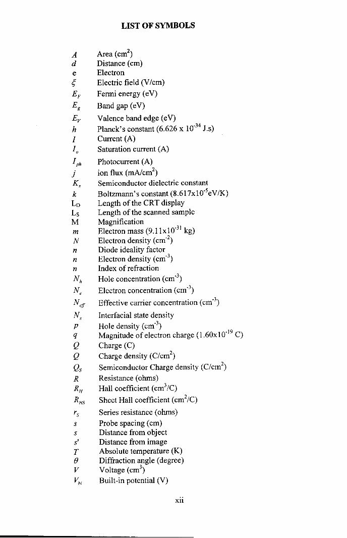
LIST OF SYMBOLS
A Area (cm2)
d Distance (em) e Electron q Electric field (V /em)
E F F enni energy ( e V)
Eg Band gap (eV)
Ev Valence band edge ( e V) h Planck's constant (6.626 X 10⁻³⁴ J.s) I Current (A) Io Saturation current (A)
!ph Photocurrent (A)
j ion flux (mA/cm2)
Ks Semiconductor dielectric constant k Boltzmann's constant (8.617xl0-5eV/K) Lo Length of the CRT display Ls Length of the scanned sample M Magnification m Electron mass (9 .11 X 1 o-31 kg) N Electron density ( cm-2
)
n Diode ideality factor n Electron density ( cm-3
)
n Index of refraction Nh Hole concentration (cm-3
)
Ne Electron concentration ( cm-3)
Neff Effective carrier concentration ( cm-3)
Ns Interfacial state density P Hole density ( cm-3
)
q Magnitude of electron charge (1.60xl0-19 C) Q Charge (C) Q Charge density (C/cm2
)
Q5 Semiconductor Charge density (C/cm2)
R Resistance (ohms) RH Hall coefficient ( cm3 /C)
RHs Sheet Hall coefficient (cm2/C)
r5 Series resistance (ohms) s Probe spacing (em) s Distance from object s' Distance from image T Absolute temperature (K) () Diffraction angle (degree) V Voltage ( cm3
)
V6i Built-in potential (V)
Xll
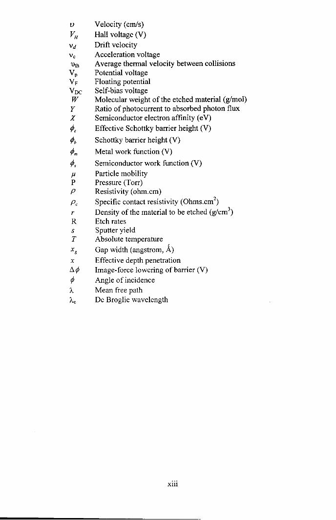
v Velocity ( crn!s) VH Hall voltage (V) v d Drift velocity Ve Acceleration voltage uth Average thermal velocity between collisions V P Potential voltage V F Floating potential V oc Self-bias voltage W Molecular weight of the etched material (g/mol) Y Ratio of photocurrent to absorbed photon flux X Semiconductor electron affinity ( e V) tPe Effective Schottky barrier height (V)
¢h Schottky barrier height (V)
tPm Metal work function (V)
tPs Semiconductor work function (V) Jl Particle mobility P Pressure (Torr) P Resistivity ( ohm.cm) Pc Specific contact resistivity (Ohms.cm2
)
r Density ofthe material to be etched (g/cm3)
R Etch rates s Sputter yield T Absolute temperature xg Gap width (angstrom, A) x Effective depth penetration ~ ¢ Image-force lowering of barrier (V) ¢ Angle of incidence 'A Mean free path Ae De Broglie wavelength
Xlll
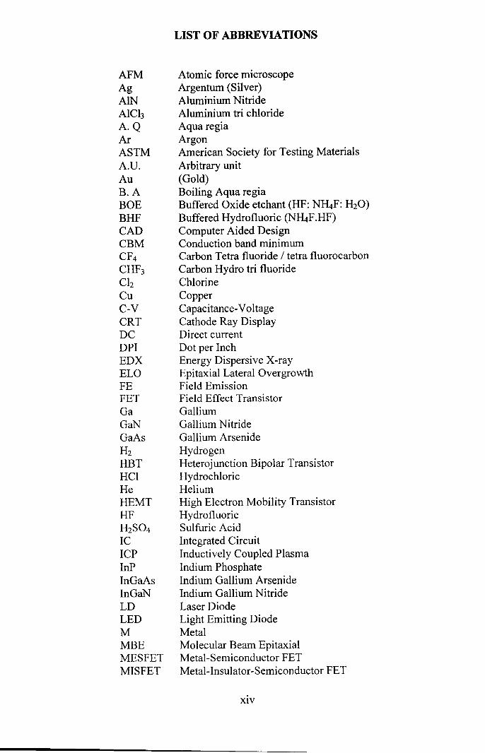
AFM Ag AlN AlCh A.Q Ar ASTM A.U. Au B. A BOE BHF CAD CBM CF4 CHF3 Ch Cu C-V CRT DC DPI EDX ELO FE FET Ga GaN GaAs H2 HBT HCl He HEMT HF H2S04 IC ICP InP InGaAs InGaN LD LED M MBE MESFET MISFET
LIST OF ABBREVIATIONS
Atomic force microscope Argentum (Silver) Aluminium Nitride Aluminium tri chloride Aqua regia Argon American Society for Testing Materials Arbitrary unit (Gold) Boiling Aqua regia Buffered Oxide etchant (HF: N~F: H20) Buffered Hydrofluoric (N~F.HF) Computer Aided Design Conduction band minimum Carbon Tetra fluoride I tetra fluorocarbon Carbon Hydro tri fluoride Chlorine Copper Capacitance-Voltage Cathode Ray Display Direct current Dot per Inch Energy Dispersive X-ray Epitaxial Lateral Overgrowth Field Emission Field Effect Transistor Gallium Gallium Nitride Gallium Arsenide Hydrogen Heterojunction Bipolar Transistor Hydrochloric Helium High Electron Mobility Transistor Hydrofluoric Sulfuric Acid Integrated Circuit Inductively Coupled Plasma Indium Phosphate Indium Gallium Arsenide Indium Gallium Nitride Laser Diode Light Emitting Diode Metal Molecular Beam Epitaxial Metal-Semiconductor FET Metal-Insulator-Semiconductor FET
XIV
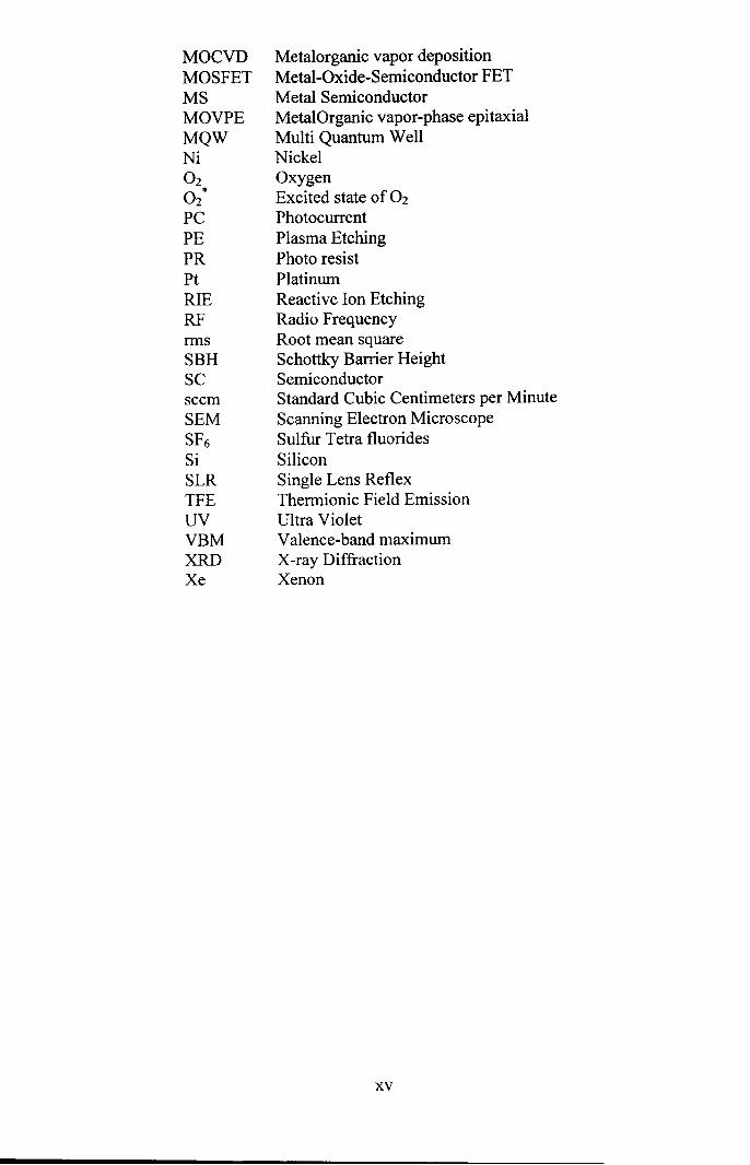
MOCVD MOSFET MS MOVPE MQW Ni 02 o2· PC PE PR Pt RIE RF rms SBH sc seem SEM SF6 Si SLR TFE uv VBM XRD Xe
Metalorganic vapor deposition Metal-Oxide-Semiconductor FET Metal Semiconductor MetalOrganic vapor-phase epitaxial Multi Quantum Well Nickel Oxygen Excited state of 02 Photocurrent Plasma Etching Photo resist Platinum Reactive Ion Etching Radio Frequency Root mean square Schottky Barrier Height Semiconductor Standard Cubic Centimeters per Minute Scanning Electron Microscope Sulfur Tetra fluorides Silicon Single Lens Reflex Thermionic Field Emission Ultra Violet Valence-band maximum X-ray Diffraction Xenon
XV
PUNARAN PLASMA YANG DIGANDINGKAN SECARA TERARUH TERHADAP GALLIUM NITRIDA
ABSTRAK
Dalam projek ini, penyelidikan difokuskan kepada kajian tentang pengaruh
pelbagai campuran plasma (H2 dan Ar) kepada Ch sebagai gas asas pada GaN
menggunakan punaran kering khususnya punaran plasma yang digandingkan secara
teraruh (ICP) untuk mendapatkan anisotropik yang tinggi, struktur dinding yang
tegak dan yang paling penting adalah untuk memperoleh kadar punaran yang tinggi.
Pertama sekali, wafer itu difabrikasi menggunakan fotolitografi dan Nikel
diselaputkan ke atas wafer n-GaN atau p-GaN melalui alat pengewapan untuk
melakukan proses 'angkat-buang'. Selepas itu, wafer dipunarkan menggunakan alat
ICP-RIE. Semasa proses itu, kadar aliran gas untuk Ar atau H2 diubahkan manakala
kadar Ch ditetapkan pada 60sccm untuk setiap eksperimen. Keadaan yang
diperlukan dalam eksperimen ini ialah 60sccm Ch dan jumlah kadar aliran 60sccm
Ar atau 30sccm H2. Manakala, kuasa ICP yang digunakan ialah lOOW, 250W kuasa
RIE dan 600W kuasa RF. Sebelum membuat punaran kepada sam pel, satu set
eksperimen yang ringkas dilakukan untuk memahami tentang perubahan dalam
komposisi gas yang mempengaruhi kadar punaran. Untuk eksperimen ini, kadar
aliran Ar diubah dari Osccm hingga 60sccm atau Osccm hingga 30sccm
menggunakan gas H2, manakala kadar aliran Ch ditetapkan pada 60sccm dan
tekanan kebuk ditetapkan pada lmTorr. Kemudian, pelbagai tekanan diubah bermula
dari lmTorr hingga 15mTorr untuk memerhatikan kesan kadar punaran dan bentuk
permukaan sampel dan akhir sekali, kuasa ICP dikenakan dari lOOW hingga 450W.
Setelah selesai fabrikasi, pencirian morfologi permukaan ditentukan menggunakan
Mikroskop Elektron yang Diimbas (SEM) dan Mikroskop Atom Dipaksa (AFM).
XVI
Mikroskop Elektron yang Diimbas (SEM) digunakan untuk mengukur kadar
punaran, anisotropik, dan struktur dinding manakala Mikroskop Atom Dipaksa
(AFM) pula digunakan untuk mencirikan morfologi permukaan sebagai Purata punca
Kuasa Dua (rms) permukaan. Dari eksperimen yang dilakukan, pertambahan 15sccm
H2 bersama dengan Ch di dalam kebuk pada tekanan 5mTorr dan 200W kuasa ICP
menyebabkan perolehan kadar punaran yang paling tinggi iaitu sebanyak 3000Aimin
untuk n-GaN dan 1900 A/min untuk p-GaN dan memplinyai permukaan yang licin
dan anisotropik. Manakala untuk pertambahan 20sccm Ar bersama dengan 60sccm
Ch pada tekanan 5mTorr dan 200W kuasa ICP, kadar punaran yang paling tinggi
didapati melebihi kadar punaran H2; 5000Aimin dan ~0.5nm dan permukaannya
masih kekallicin; ~0.5nm for n-GaN and ~0.7nm for p-GaN. Oleh itu, pertambahan
H2 kepada plasma klorin menyebabkan permukaan yang dipunar lebih licin dari Ar,
manakala pertambahan Ar pula menyebabkan kadar punaran yang paling tinggi
dicapai dalam eksperimen ini.
XVll
INDUCTIVELY COUPLED PLASMA ETCIITNG ON GaN
ABSTRACT
In this project, the research mainly focused on the investigation of the
influence of the various plasma mixtures (H2 and Ar) in Ch-based on GaN using dry
etching majoring in Inductively Coupled Plasma etching to obtain highly anisotropic,
vertical sidewalls structures and most importantly, highly etch rates for optimum
device performance. First of all, the wafer was fabricated using the conventional
photolithography method and the Ni metals were coated onto the n-GaN or p-GaN
wafer through evaporator equipment to make lift-off process. After that, the wafer
was etched using ICP-RIE machine. During the process, the gas flow rates for Ar or
H2 were varied while Cb rates were held constant at 60sccm for all experiments. The
conditions consisted of 60sccm of Ch and the total flow rate 60sccm of Ar or 30sccm
of H2• Meanwhile, ICP power, RIE power and RF power was held at lOOW, 250W
and 600W respectively. Prior to etching patterned samples, a simple set of
experiments were conducted to get an understanding of how changes in gas
composition affect the etch rate. For this experiment, the flow rate was varied from
Osccm to 60sccm using Ar gases or from Osccm to 30sccm using H2 gases,
meanwhile the Ch flow rates and the chamber pressure were held constant at 60sccm
and lmTorr, respectiveiy. Then, the various pressures were varied starting of lmTorr
to 15m Torr to observe the effect of etch rates and the roughness of surface and lastly,
the ICP power applied from lOOW to 450W. After that, the wafer will be
characterized using SEM and AFM. SEM will be used to measured the etch rates,
anisotropic etch profiles and sidewalls meanwhile AFM has been used to quantify
the etched surface morphology as root-mean-square (rms) roughness. From our
XVlll

experiments, the addition of 15sccm H2 together with Chin the chamber at 5mTor of
pressure and 200W ICP power obtained high etching rate about 3000Aimin for n
GaN and 1900Aimin for p-GaN and smooth anisotropic pattern. Meanwhile, for
addition of 60sccm Ar together with 20sccm Ch at pressure of 5mTorr and 20W ICP
power resulting the highest etch rates, better than the addition of H2; 5000Aimin for
n-GaN and 3300Aimin for p-GaN, while maintaining the smooth surface; -0.5nm for
n-GaN and -0.7nm for p-GaN. Hence, it was found that the addition of H2 to
chlorine plasma distributed a smooth etched surface better than Ar, while addition of
Ar resulting the highest etching rates for this research.
XIX
1.1 Introduction
CHAPTERl INTRODUCTION
This chapter was devoted to issues and theories that were relevant to the work
in this research. This chapter begins with an elaboration about the fundamental
properties of GaN, lack of suitable etchants and dry etching and ended the chapter
with research objectives of this work.
1.2 III-V Nitrides for Device Applications
For the last three decades or so, the III-V semiconductor material system has
been viewed as highly promising for semiconductor device applications at blue and
ultraviolet (UV) wavelengths in much the same manner that its highly successful As-
based and P-hased counterparts have been exploited for infrared, red and yellow
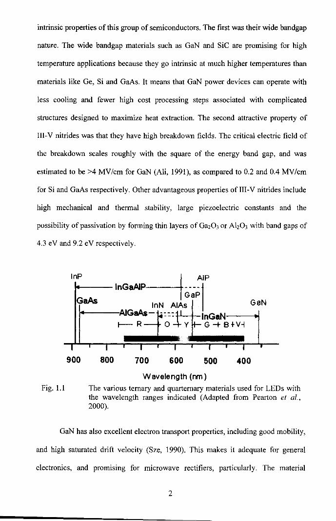
wavelength as shown in Figure 1.1. As members of the III-V nitrides family, AlN,
GaN, InN and their alloys were all wide band gap materials, and can crystallize in
both wurtzite and zincblende polytypes. Wurtzite GaN, AlN and InN have direct
room temperature bandgaps of 3.4 eV, 6.2 eV and 1.9 eV, respectively (Figure 1.2).
In cubic form, GaN and InN have direct bandgaps, while AlN was indirect. In view
of the available wide range of direct bandgaps, GaN alloyed with AlN and InN may
span a continuous range of direct bandgap energies throughout much of the visible
spectrum well into the ultraviolet wavelengths. This makes the nitride system
attractive for optoelectronic device applications, such as light emitting diodes (LEDs ),
laser diodes (LDs), and detectors, which were active in the green, blue or UV
wavelengths (Strite, 1992).
Another area gaining a lot of attention for III-V nitrides was high
temperature/high power electronics (Pearton, 2000). The interest stems from two
1
intrinsic properties of this group of semiconductors. The first was their wide bandgap
nature. The wide bandgap materials such as GaN and SiC are promising for high
temperature applications because they go intrinsic at much higher temperatures than
materials like Ge, Si and GaAs. It means that GaN power devices can operate with
less cooling and fewer high cost processing steps associated with complicated
structures designed to maximize heat extraction. The second attractive property of
III-V nitrides was that they have high breakdown fields. The critical electric field of
the breakdown scales roughly with the square of the energy band gap, and was
estimated to be >4 MV/cm forGaN (Ali, 1991), as compared to 0.2 and 0.4 MV/cm
for Si and GaAs respectively. Other advantageous properties of III-V nitrides include
high mechanical and thermal stability, large piezoelectric constants and the
possibility of passivation by forming thin layers of Ga20 3 or Ah03 with band gaps of
4.3 eV and 9.2 eV respectively.
Fig. 1.1
lnP
GaAs -t AlP
lnGaAIP ----1 GaP InN AlAs GaN
~+---AIGaA.s- -:::tL- lnGaN t-- R 0-+ Y G -t 8 +V-l
900 800 700 600 500 400
Wavelength (nm)
The various ternary and quarternary materials used for LEDs with the wavelength ranges indicated (Adapted from Pearton et al., 2000).
GaN has also excellent electron transport properties, including good mobility,
and high saturated drift velocity (Sze, 1990). This makes it adequate for general
electronics, and promising for microwave rectifiers, particularly. The material
2
properties associated with high temperature, high power, and high frequency
application of GaN and several conventional semiconductors are summarized in
Table 1.1. It was anticipated that GaN may eventually prove to be superior to SiC in
this area.
> llJ -uf'
!; l
7.0
Wurtzitie Zincblende a-A IN
]; ... ••• J3-AIN
4.0
3.0
2.0
a-InN
300K 1.0 ................. ~i-'-'-"""""+ ........ ...,.,..·U-....... ~1-W-"""""+ ........ "* ...... ""'
a.o 1.2 a.4 a.• a.a u 4.4 •·• u a.o Lattice Constant (A)
Fig. 1.2 Bandgap of hexagonal (a-phase) and cubic (b-phase) InN, GaN, and AlN and their alloys versus lattice constant ll{) (Adapted from Pearton eta/., 2000).
Table 1.1 Comparison of 300 K semiconductor material properties (Adapted from Sawin, 1985).
Property Si GaAs 4H-SiC GaN Bandgap Eg ( e V) 1.12 1.42 3.25 3.40 Breakdown Field E8 (MV/cm) 0.25 0.4 3.0 4.0 Electron Mobillity Jl (cm2N.s) 1350 6000 800 1300
Maximum Velocity Ys (107 cm/s) 1.0 2.0 2.0 3.0
Thermal Conductivity x (W/cm•K) 1.5 0.5 4.9 1.3
Dielectric Constant E 11.8 12.8 9.7 9.0
CFOM = XEJlYsEs21(XE/J.YsEs2)si 1 8 458 489 (CFOM= Combined Figure of Merit for high temperature/high power/high frequency applications).
3
1.2.1 Gallium Nitrides
Of all the III-V nitrides, gallium nitride or GaN was considerably the most
intensely studied among the III-V nitride semiconductors. GaN was a direct and
wide band gap semiconductor when compared to the more widely known Si as well
as GaAs and SiC, to name among a few. With its superior radiation hardness and
chemical stability, together with its large band gap characteristic, these properties
have made GaN a suitable semiconductor material for device applications in the
high-temperature and caustic environment as well as in space applications. GaN was
also an attractive candidate for protective coatings due to its radiation hardness
(Strite, 1992). Its wide band gap make it go intrinsic at a much higher temperature
than materials like Ge, Si and GaAs, i.e. the intrinsic carrier concentration at any
given temperature decreases exponentially with band gap, and therefore GaN and
similar wide band gap materials are attractive for high temperature applications.
Moreover, due to its many attractive features like higher sheet charge densities,
higher mobilities, better charge confinement, and higher breakdown voltages, GaN
was also a potential candidate for the application in electronic devices such as high
temperature, high power and high frequency transistors (Ali, 1991, Sze, 1990,
Pearton, 1999).
Unlike SiC, another widely studied large band gap semiconductor with
demonstrated n- and p- type doping and excellent power device performance, one
advantage of GaN as well as III-V nitrides was that they form direct band gap
heterostructures, have better ohmic contacts and heterostructures., which eventually
made III-V nitrides or GaN a more promising candidate than SiC in terms of
application devices in optoelectronics (Razeghi, 1996).
4

The transparency of high quality GaN at wavelengths longer than the band
gap make it an ideal material for fabricating photodetectors capable of rejecting near
infrared and visible regions of the solar spectrum while retaining near unity quantum
efficiency in the UV. Besides, in optoelectronics, GaN was primarily of interest for
its potential as a blue and UV light emitter (Strite, 1992). GaN was most commonly
observed as the wurtzite 2H polytype but it can also crystallize into a metastable
zinc-blende 3C structure (Mizuta, 1986, Davis, 1989, Petrov, 1992, Strite, 1993).
However, another structure, which was the rocksalt, or NaCl structure can also be
induced in the GaN under very high pressures (Morkoc, 1999).
In general, GaN normally crystallizes in the wurtzite crystal structure, where
it was grown on hexagonal substrates. On the other hand, the zinc blende structure
can be grown on cubic substrates.
1.2.2 Lack of suitable etchant
The chemical stability of GaN provides a technological challenge, for
example like when it comes to lithography (Maruska, 1996) where there have been
many reports describing the resistance of GaN films to the conventional wet etching
techniques used in semiconductor processing. There was no reliable wet chemical
etchant that has been found forGaN. Maruska and Tietjen (1996) reported that GaN
was insoluble in H20, acids, or bases at room temperature; however GaN did
dissolved in hot alkali solutions, but at a very slow rate. Due to the difficulties of
developing an established chemical etching process for GaN despite the efforts of
many researchers, the attentions has shifted to dry etching; reactive ion etching (RIE)
and high density plasma etching as the dominant patterning technique for III-V
materials including GaN.
5
1.2.3 Dry etching
In general, many have reported excellent etch anisotropies suggesting that
RIE was a highly suitable technology forGaN-based device processing. Reactive ion
etching (RIE) was one of the dry etching techniques in common usage, which utilizes
both the chemical and physical components of an etch mechanism. RIE plasmas are
typically generated by applying radio frequency (rf) power of 13.56 MHz between
two parallel electrodes in a reactive gas. Etching was typically performed at low
pressures, ranging from a few mTorr up to 200 mTorr, which promotes anisotropic
etching due to increased mean free paths and reduced collisional scattering of ions
during acceleration in the sheath. RIE was by far the most popular dry etching
technique used for conventional III-V materials, and takes advantage of the fact that
there was a synergism between the physical and chemical etching mechanisms.
The use of high-density plasma etch systems, such as inductively coupled
plasma (ICP) (Pearton, 2000) and electron cyclotron resonance (ECR), has resulted
in improved etch characteristics for the III-V nitrides as compared to RIE. This
observation was attributed to plasma densities which were 2-4 orders of magnitude
higher than RIE thus improving the III-N bond breaking efficiency and the sputter
desorption of etch products for the surface. Additionally, since ion energy and ion
density can be more effectively decoupled, plasma induced damage was more readily
controlled.
High density ICP plasmas were formed in a dielectric vessel encircled by an
inductive coil into which rf power was applied. The alternating electric field between
the coils induces a strong alternating magnetic field trapping electrons in the centre
ofthe chamber and generating plasmas with uniform density and energy distribution.
6
By keeping ion and electron energy low, we can obtain low damage etching while
maintaining fast etch rates.
Anisotropy was achieved by superimposing a rf bias on the sample. Generally,
etch characteristics were dependent upon plasma parameters including ion energy
(controlled by rf chuck power), plasma density (controlled by ICP source power),
and operation pressure (the change in collisional frequency can result in changes in
both ion energy and plasma density). ICP etching was generally believed to have
several advantages including easier scale-up for production, improved plasma
uniformity and lower cost of operation.
Good results for the III-V nitrides have been obtained in chlorine-based
plasma under high ion energy conditions where the 111-N bond breaking and the
sputter desorption of etch products were most efficient. Unfortunately, the high
energy plasma may induce significant damage and degrade both electrical and optical
device performances. Lowering the ion energy and increasing the chemical activity
in the plasma often results in much slower etch rates and less anisotropic profiles. It
was necessary to pursue alternative etch platforms which combine high quality etch
characteristics with low damage for III-V nitrides.
Additive gases have been introduced in order to obtain a vertical sidewall,
since etching with pure Ch generally leads to severe undercuts (Rommel, 2002). Cho
et al. reported binary gas chemistries such as Ch/Ar, Ch/N2, Ch/H2 and concluded
that ICP discharges were well-suited to achieving smooth etched surfaces when
appropriate plasma condition were used. Previous study has demonstrated that
unintentionally doped successfully etched by ICP using Ch/Ar as the etching gases
(Sheu, 1999). It has been shown that one can achieve a highly anisotropic etch with a
high etching rate and smooth surface morphology by using Ch/ Ar as the etching
7
gases. During such ICP etching, Ch was used to provide reactive Cl radicals,
chemically react with GaN to form volatile etch products, and then desorbed from
the sample surface. On the other hand, Ar was used to perform physical etching so as
to achieve an anisotropic etching. Ch/H2 mixture has also bee studied since the
inclusion of H2 in the plasma was found to increase etch rates and also improve
surface morphology.
To date, only a few reports on the effect of gas additives to Ch plasmas have
been reported. Therefore, the effects of gas additives such as H2 and Ar on the etch
characteristics of an inductively coupled Ch-based plasma have been chosen as a
collection of recipes for this research. Each gas additive had unique effects on the
etch rate, etch anisotropy, surface roughness and sidewall morphology, all of which
require reliable control for device fabrication.
1.3 Research Objective
As the circuit complexity increases and device dimensions decreases, it was
very necessary to choose right technique in order to get a highly anisotropic result. In
this project, the research mainly focused on the investigation of the dry etching
majoring in Inductively Coupled Plasma etching on GaN. To achieve the main
objectives, several sub objectives have been identified:
1. To obtain recipes using gas combination (Ar and H2) in Ch-based
on GaN.
2. To study the effects of Ch/Ar mixture on n-GaN and p-GaN
etching.
3. To investigate the effects of Ch/H2 mixture on n-GaN and p-GaN
etching.
8
4. To get the formation of highly anisotropic and sidewalls structures.
5. To determine the smooth surfaces after etching to avoid stress
concentration for selected recipes.
1.4 Outline of the thesis
The content of this thesis was organized as follows:-
The next chapter, Chapter 2, will cover GaN-related matters and theory that
were relevant to the work in this research.
Chapter 3 was devoted to the instrumentation employed in this work. An
explanation on the procedures and methods used, and also some principles
underlying the operation of the instruments were covered.
Chapter 4 will discuss include the main topic/theory which was associated in
the fabrication process as well as the discussions of methods used in obtaining the
results for this research project.
In Chapter 5 and 6, the results of the effects of Ch/ Ar and Ch/H2 mixture on
n-GaN and p-GaN etching from this research were presented, analysed and discussed.
The final chapter, Chapter 7 concludes the thesis with a summary of the
research work. Conclusion of the results obtained and a few suggestions for future
research were included.
9
CHAPTER2 THEORY OF PLASMA ETCIDNG
2.1 Introduction
This chapter is devoted to the theories that are relevant to the work in this
research such as general principles of etching; wet and dry etching, the process of
etching and the fundamentals of plasmas. Meanwhile, the types and the technique of
dry etching including the literature review of Ch-based plasma etching are explained
at last topics in this chapter.
2.2 Etching
"Etching" is used to describe any technique by which material can be
uniform removed from a wafer, or locally removed as in the transfer of patterns
during fabrication of a microcircuit. Etching processes are divided into two major
groups; wet etching (e.g. liquid chemicals) and dry etching (e.g. reactive gas
plasmas). The basic mechanism of wet chemical etches of semiconductors is the
formation of an oxide, or oxides on the surface, and the subsequent dissolution of the
oxidized products by either acids or bases (Manos, 1989). The main advantage of this
etching method is its simplicity, high selectivity, high throughput and low cost.
However, these advantages do not apply to nitrides based material. GaN for example,
electrolysis etches slowly at room temperature in hot alkalis and complex
electrolytically using NaOH. Because of all this difficulties in obtaining reliable wet
etching process, much work on nitride based etching are concentrated on dry etching
processes. As such, we will only discuss briefly on wet etching and elaborate on the
progress of dry etching throughout this chapter.
10
2.3 Wet Etching
2.3.1 General Principles of Wet Etching
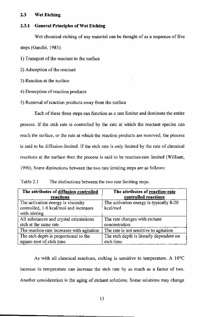
Wet chemical etching of any material can be thought of as a sequence of five
steps (Gandhi, 1983):
1) Transport ofthe reactant to the surface
2) Adsorption of the reactant
3) Reaction at the surface
4) Desorption of reaction products
5) Removal of reaction products away from the surface
Each of these three steps can function as a rate limiter and dominate the entire
process. If the etch rate is controlled by the rate at which the reactant species can
reach the surface, or the rate at which the reaction products are removed, the process
is said to be diffusion-limited. If the etch rate is only limited by the rate of chemical
reactions at the surface then the process is said to be reaction-rate limited (William,
1990). Some distinctions between the two rate limiting steps are as follows:
Table 2.1 The distinctions between the two rate limiting steps.
The attributes of diffusion controlled The attributes of reaction-rate reactions controlled reactions
The activation energy is viscosity The activation energy is typically 8-20 controlled, 1-6 kcal/mol and increases kcal/mol with stirring All substances and crystal orientations The rate changes with etchant etch at the same rate concentration The reaction rate increases with agitation The rate is not sensitive to agitation The etch depth is proportional to the The etch depth is linearly dependent on square root of etch time etch time
As with all chemical reactions, etching is sensitive to temperature. A 1 0°C
increase in temperature can increase the etch rate by as much as a factor of two.
Another consideration is the aging of etchant solutions. Some solutions may change
11
composition over time, depending on temperature and storage. All of these factors
must be considered in establishing reproducible and controllable etching processes
(William, 1990).
2.4 Dry Etching
2.4.1 Dry Processing
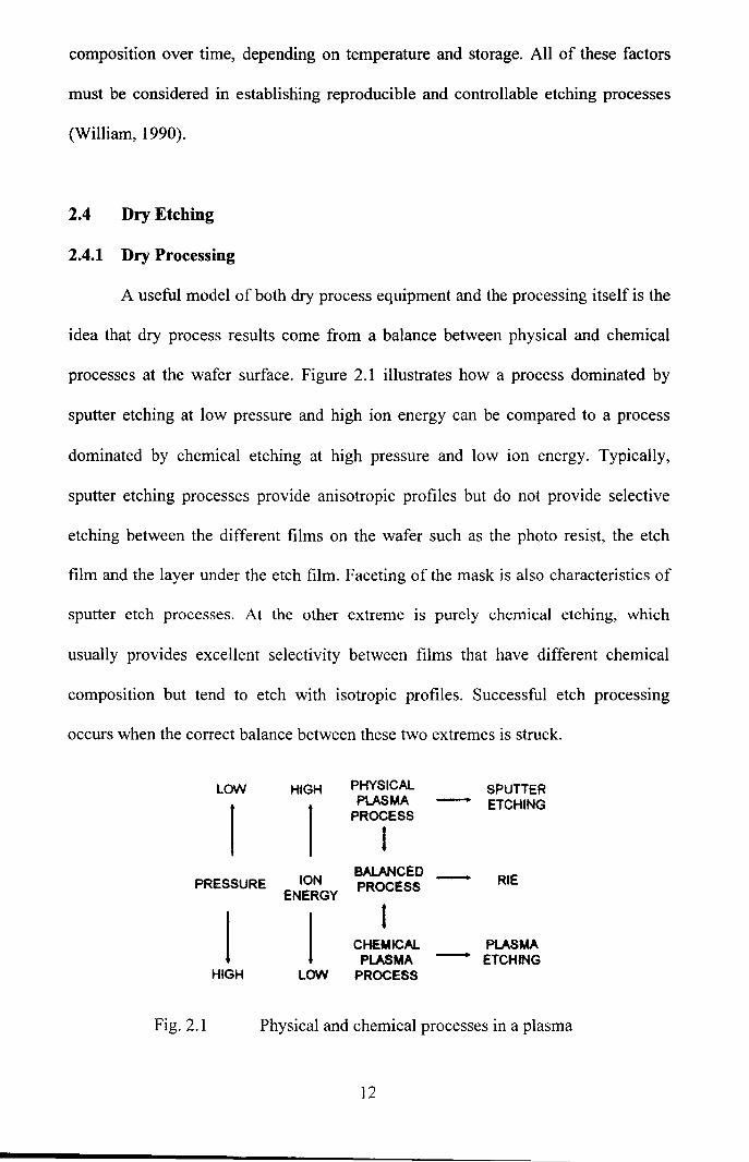
A useful model of both dry process equipment and the processing itself is the
idea that dry process results come from a balance between physical and chemical
processes at the wafer surface. Figure 2.1 illustrates how a process dominated by
sputter etching at low pressure and high ion energy can be compared to a process
dominated by chemical etching at high pressure and low ion energy. Typically,
sputter etching processes provide anisotropic profiles but do not provide selective
etching between the different films on the wafer such as the photo resist, the etch
film and the layer under the etch film. Faceting of the mask is also characteristics of
sputter etch processes. At the other extreme is purely chemical etching, which
usually provides excellent selectivity between films that have different chemical
composition but tend to etch with isotropic profiles. Successful etch processmg
occurs when the correct balance between these two extremes is struck.
LOW HIGH PHYSICAL SPUTTER PlASMA - ETCHING
I I PROCESS
1 ION
BALANCED - RIE PRESSURE PROCESS ENERGY
I I 1 CHEMICAL PlASMA PLASMA - ETCHING
HIGH LOW PROCESS
Fig. 2.1 Physical and chemical processes in a plasma
12
2.4.2 Plasma Fundamentals
Plasma is a gas which contains equal numbers of positive and negative
charges; neutral atoms, radicals, or molecules; in addition to photons emitted from
excited species. Radicals are molecule fragments with unsaturated bonds. Positive
charge carriers are mostly singly ionized atoms, radicals, or molecules created by
impact with energetic electrons. The majority of negative charges are free electrons.
In the presence of atoms with high electron affinity, negatively charged ions can be
created when these capture plasma electrons. Neutral atoms, radicals, and molecules
can be at ground or excited state. Photons are emitted when excited species lose
energy via spontaneous transitions to lower energy states. This latter process is the
basis for the "glow" of the discharge.
Plasma can be created by applying an electric field of sufficient magnitude to
a gas. The process can be initiated by an incident electron which gains kinetic energy
from the applied electric field. The probability for the electron to collide with and
transfer energy to a gas atom or molecule depends upon the electron energy, the gas
pressure, and the dimensions of the plasma chamber. When a collision occurs, it
results in ionization, excitation, or fragmentation of gas molecules. An ionizing
collision generates an electron-ion pair. The two new charged particles are
accelerated in the electric field and can in tum collide with and ionize other gas
particles. As this process continues, the gas breaks down and plasma is created. The
charged particles can be neutralized by recombination within the plasma or at the
chamber walls. For plasma to be sustained, however, the rate of ionization of gas
atoms or molecules must be equal to the rate of electron and ion recombination.
Collisions can result in fragmentation of gas molecules into atoms or
molecules of smaller size or, for smaller electron energies, in excitation of atoms or
13
molecules to higher energy levels. Some important chemical and physical processes
that occur in plasma are summarized in Table 2.2 (Sawin, 1985). At thermal
equilibrium the particles can be assumed to move randomly at an average thermal
velocity between collisions, approximated by
(2.1)
where k is Boltzmann's constant (k = 8.62xl0-5 eV/K), T the absolute temperature,
and m the particle mass. Because of their very small mass, electrons travel at much
higher thermal velocity than gas atoms or molecules. The motion of charged particles
under the influence of an electric field is described in terms of a drift velocity, vd,
given by
(2.2)
where f1 is the particle mobility, and E the electric field.
Electrons also drift at a much higher velocity than ions. As electrons gain
kinetic energy from the electric field, their effective temperatures increase above the
gas temperature. While the temperature of the atoms and molecules in the gas
remains near ambient, electrons can attain high average energies, typically 1-10 e V,
corresponding to an effective electron temperature of 104-105 K (Fonash, 1985).
This energy is transferred to the gas by collision processes in which ions and
highly reactive species are created. It is this property of the plasma that allows high-
temperature type reactions to occur at low ambient temperatures and permits the use
of temperature sensitive materials such as organic resist masks for etching. The
average distance travelled by particles between collisions, called the mean free path A.,
depends on the species and gas pressure following the relation
...1= 5x10⁻³ (em) p
14
(2.3)
where P is the pressure in Torr. The electron density in plasmas of interest ranges
from 109 - 1012 cm·3. It follows that the degree of ionization is very small; in typical
reactors used for etching only 104 to 10·7 ofthe gas molecules are ionized (El Kareh,
1995).
Table 2.2 Important reactions in plasma (David, 1999).
Reaction Example
Positive ionization Ar + e ~ Ar+ + 2e 02 + e ~ 02 + + 2e
Dissociative CF4 +e ~ CF3+ + F + 2e
Fragmentation CF3Cl + e ~ CF3 + Cle· C2F6 + e ~ 2CF3 + e
Dissociative attachment CF4+ e ~ CF3 + F Dissociative ionization with attachment CF4+e~CF3+F+e
Excitation 02 + e ~ 02* + e· Photoemission 02* ~ 02 + hv
02 * is the excited state of 0 2
2.4.3 Paschen Law (Ledernez, 2009)
The first Townsend coefficient a is the probability to ionize a gas neutral by
collision per unit length of path, i.e. it is the number of collision per unit length of
path times the ionization probability per collision. Hence:
a = ~ X exp (-_;) A. E.
(2.4)
with 'Ae the electron mean free path, Ei the ionization energy of the gas, Ee the
electron energy colliding with the gas neutral. Equation (2.4) is more commonly
known as (Cobine, 1958): a= Ap exp (-i) with Ee = e'AeE. Assuming that the
electric field is uniform before the gas breakdown (E = Vb I d), Eq. (2.4) can be
transformed to:
Bpd V ln- = C+ In (pdJ (2.5)
15
With A. = kts T , one can deduce: GeJ>
and the Paschen coefficients:
(J.
A=--...!! kT
a .E. B:~
ekT
C=ln(~T)
(2.6)
(2.7)
(2.8)
where <Jei is the electron impact ionization cross section (in m\ Ei is the ionization
energy of the gas (in J), e the elementary charge (in C), k the Boltzmann constant, T
the temperature (inK).
2.4.4 The formation of a DC voltage. (V erdonck, 1990)
Plasma is a (partially) ionized gas. In the plasmas we deal with, free electrons
collide with neutral atoms/molecules and, through a dissociative process, they can
remove one electron from the atom/molecule, which gives a net result of 2 electrons
and 1 ion. Depending on the energy of the incoming electron, this collision can result
also in other species, such as negative ions, because of electron association, excited
molecules, neutral atoms ".nd ions. The light emitted by the plasma is due to the
return of excited electrons to their ground state. As the energies between the
electrons states are well defined for each element, each gas will emit light at specific
wavelengths, which will give us the possibility to analyse the plasma.
The power is applied to the lower or the upper electrode (or in some special
cases to the reactor walls). In general the frequency of the applied power is 13.56
MHz. A so-called dark sheath is formed in the neighbourhood of all surfaces in the
reactor, electrodes and wails. This dark sheath can be considered as some kind of
16
------------- --·-
dielectric or a capacitor. So, the applied power is transmitted to the plasma through a
capacitor.
At frequencies between 1 MHz and 100 MHz, the free electrons are able to
follow the variations of the applied electric field and, unless they suffer a collision,
they can gain considerable e energy, of the order of some hundred e V. On the other
hand, in this frequency range, the movement of the much heavier (positive) ions is
very little influenced (one may simplify that they are not influenced) by these electric
fields: their energy comes completely from the thermal energy of the environment
and is of the order of a few hundredths of an eV (i.e., -0.01eV).
In the pressure range of these plasmas, from a few mTorr to a few hundreds
of mTorr, the electrons will travel much longer distances than the ions, and in this
way, they will much more frequently collide with the reactor walls and electrodes
and consequently be removed from the plasma. This would leave the plasma
positively charged. However, plasmas remain neutral. To guarantee this neutrality, a
DC electric field has to be formed in such a way that the electrons are repelled from
the walls. The capacitor between the power generator and the electrode helps to form
the DC charge. During the first few cycles, electrons generated in the plasma escape
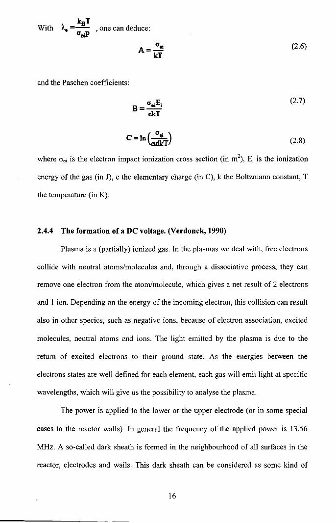
to the electrode and charge the capacitor negatively. In this way, a negative DC bias
voltage is formed on the electrode, which repels the electrons. The AC voltage
becomes then superposed on this negative DC voltage as shown in Figure 2.2.
Free electrons escape from the plasma in higher numbers to the walls than
ions do. So, one also needs a certain DC voltage to repel the electrons from the walls.
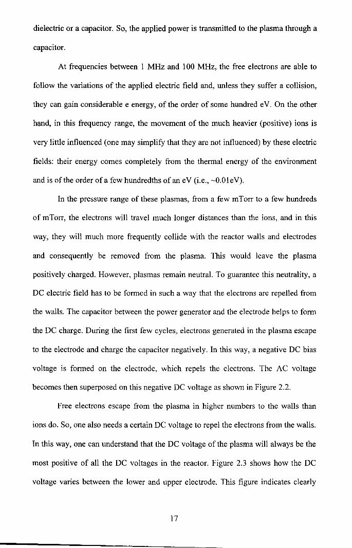
In this way, one can understand that the DC voltage of the plasma will always be the
most positive of all the DC voltages in the reactor. Figure 2.3 shows how the DC
voltage varies between the lower and upper electrode. This figure indicates clearly
17
how the electrons are repelled from the walls and electrode towards the plasma. The
ions are attracted towards the wall. However, because of their large mass, only the
ions which arrive "by coincidence" at the interface of the plasma with the dark
sheath will be attracted towards the electrodes or the walls. Within the plasma, the
ions are not influenced by the electric fields and move randomly.
- v Fig. 2.2 DC and AC voltage on the powered (Adapted
from Verdonck, 1990)
LOW8r electrode
Upper electrode
- VDC Fig. 2.3
a
a 1 interface plasma-dark aheath generated by lower electrode
b a interface plas~~a-dark sheath generated by upper electrode
DC voltage in the plasma reactor in RIE mode (Adapted from Verdonck, 1990)
18
In most reactors, one can clearly observe this so-called dark sheath as a
region with less luminosity than the bulk of the plasma. In this region, the density
and energy of the free electrons is lower. Therefore, less collisions with molecules
will occur, causing less excitations of electrons (bound to molecules) and therefore
less photons will be emitted from this region.
2.4.5 Influence of DC Bias (V erdonck, 1990)
The value of the DC voltage is influenced by many parameters. It depends in
the first place on the dimensions of the etching reactor. It also depends on the plasma
process (gas, flow, pressure, power etc).
2.4.5.1 Influence of the dimensions of the reactor and etching mode
One can demonstrate that:
(2.9)
with the Voc the voltage drop between plasma and electrode 2, A1 the area of
electrode 1, A2 the area of electrode 2, n an exponential factor, which is typically
between 1 and 2. Formula 2.9 is valid for whatever electrode is powered. If electrode
1 is powered and electrode 2 is grounded, V oc is in the case the DC potential of the
plasma.
One can provt that n = 1 or that n = 2, depending on the (very reasonable)
assumptions one makes about the plasma. Anyway, the modulus of the DC voltage
will increase with the ratio of grounded surface area. In RIE systems, the powered
electrode has in general much less area than the grounded surfaces, resulting in a
large negative DC voltage on the lower electrode. The consequences on the etching
19
results will be discussed later. In PE systems, the upper electrode is powered and the
lower electrode is in general grounded, together with the walls. This results in
general in a small voltage drop between plasma and lower electrode. One can
decrease the voltage drop between plasma and electrode even more, when one leaves
the electrode floating i.e. no electrical connection is made to the lower electrode.
2.4.5.2 Influence of the plasma parameters
In general, the dimensions of the reactor are fixed. In this case, one can
influence the DC voltage by the process parameters. One should remember that the
DC voltage is created to repel electrons. Therefore, the higher the electron density
and the higher the electron energy, the higher the modulus of the DC voltage will be:
a more negative voltage is necessary to repel a larger number of electrons, with
higher energies. Using this reasoning, one is able to predict the tendencies of the DC
bias voltage.
2.4.5.2.1 Gases and Flow
The electronegativity of used gases is a determining factor. When all other
process parameters remain constant, the electronegativity of the gas will determine
the DC voltage. Gases with low electronegativity, such as 0 2, N2 etc. have very
negative DC bias voltages. Fluorine, chlorine and bromine containing gases are much
more electronegative: the atoms of group VII are very prone to absorb any free
electron which passes nearby. In this way, these gases decrease the density of the
free electrons in the plasma (increasing the number of negative ions). Fluorine
containing gases are more electronegative than chlorine containing gases, which are
more electronegative than bromine containing gases. SF 6 is a very electronegative
20
gas: its main use is in fact as an insulator gas in places with high electric fields, e.g.
around linear accelerators. When all other plasma parameters remain the same, the
DC voltage of SF 6 plasma can be a factor of 10 less than the DC voltage of N2
plasma. The absolute flow ofthe gases does in general not affect the DC voltage. If a
mixture of gases is used, the DC bias will be a monotonically increasing function of
the relative flows of the gases. In general, the DC bias tends to become rapidly more
negative when a small flow of a gas with low electronegativity is entered in the
plasma. Small flows of electronegative gases do not influence the DC bias very
much.
2.4.5.2.2 Pressure
The pressure of the plasma does also influence the DC bias voltage, but to
explain its influence is a little more complicated. At higher pressure, more molecules
are available for the electrons to collide with and to generate a new free electron -
and a positive ion. In this way, an increase in pressure would increase the number of
free electrons, turning the DC voltage more negative. On the other hand, an increase
in pressure increases the density of species, i.e. it decreases the mean free path of the
electrons before colliding. In this way, the electrons will gain less energy before
colliding. This decrease in energy results in less formation of a new electron-positive
ion pair. This mechanism decreases the formation of free electrons and ions. So, one
has two tendencies in opposite ways. In the pressure ranges used ior plasma etching,
one can observe that in the 1- (approximately) 100 m Torr range, the number of free
electrons increases, the plasma becomes more dense with increasing pressure. At
higher pressure, the plasma density decrease with pressure. The DC voltage is also a
function of the energy of the free electrons. At higher pressure, electrons suffer more
21
collisions, therefore they gain less energy between collisions. The electron energy
decreases with pressure. Taking all these mechanisms in account, one can understand
that the DC bias voltage becomes less negative with increasing pressure.
2.4.5.2.3 Power
The influence of power is straightforward: an increase of power increases
both the density and the energy of the free electrons. Therefore, the DC voltage
becomes more negative with increasing power.
2.4.6 Sheath Formation
A simple plasma-etch reactor is shown in Figure 2.4. It consists of a grounded
electrode which is typically connected to the chamber walls, a second electrode to
which power is applied, and a partially evacuated chamber which contains a low
pressure of a suitable mixture. Most systems use rf rather than de power to avoid
charge accumulation on insulator surfaces. The rf amplitude is in the range of 700-
1000 V, and its frequency is typically 13.56 MHz. At such a frequency, most
electrons oscillate between the electrodes, increasing the average electron energy and
probability of electron-gas collisions. The rf power source is separated from the
second electrode by a coupling capacitor to block de current components. While the
plasma chamber as a whole is neutral, recombination of charges at boundary surfaces
surrounding the plasma causes charge depletion near these boundaries and the
formation of a boundary layer called the sheath. The resulting gradient in charges
gives rise to a net diffusion of carriers to the boundaries. Since electrons diffuse
faster than ions, more electrons leave the plasma initially. Consequently, an excess of
22
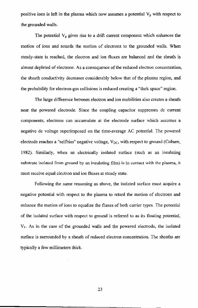
positive ions is left in the plasma which now assumes a potential V P with respect to
the grounded walls.
The potential V P gives rise to a drift current component which enhances the
motion of ions and retards the motion of electrons to the grounded walls. When
steady-state is reached, the electron and ion fluxes are balanced and the sheath is
almost depleted of electrons. As a consequence of the reduced electron concentration,
the sheath conductivity decreases considerably below that of the plasma region, and
the probability for electron-gas collisions is reduced creating a "dark space" region.
The large difference between electron and ion mobilities also creates a sheath
near the powered electrode. Since the coupling capacitor suppresses de current
components, electrons can accumulate at the electrode surface which assumes a
negative de voltage superimposed on the time-average AC potential. The powered
electrode reaches a "selfbias" negative voltage, Voc, with respect to ground (Coburn,
1982). Similarly, when an electrically isolated surface (such as an insulating
substrate isolated from ground by an insulating film) is in contact with the plasma, it
must receive equal electron and ion fluxes at steady state.
Following the same reasoning as above, the isolated surface must acquire a
negative potential with respect to the plasma to retard the motion of electrons and
enhance the motion of ions to equalize the fluxes of both carrier types. The potential
of the isolated surface with respect to ground is referred to as its floating potential,
Vf. As in the case of the grounded walls and the powered electrode, the isolated
surface is surrounded by a sheath of reduced electron concentration. The sheaths are
typically a few millimeters thick.
23
gas inlet
Fig. 2.4
--
--Schematic of simplified plasma etch reactor.
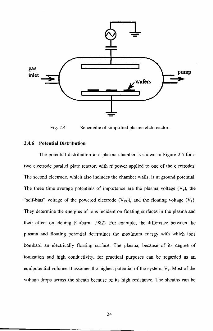
2.4.6 Potential Distribution
The potential distribution in a plasma chamber is shown in Figure 2.5 for a
two electrode parallel plate reactor, with rf power applied to one of the electrodes.
The second electrode, which also includes the chamber walls, is at ground potential.
The three time average potentials of importance are the plasma voltage (V p), the
"self-bias" voltage of the powered electrode (Voc), and the floating voltage (Vf).
They determine the energies of ions incident on floating surfaces in the plasma and
their effect on etching (Coburn, 1982). For example, the difference between the
plasma and floating potential determines the maximum energy with which ions
bombard an electrically floating surface. The plasma, because of its degree of
ionization and high conductivity, for practical purposes can be regarded as an
equipotential volume. It assumes the highest potential of the system, V p· Most of the
voltage drops across the sheath because of its high resistance. The sheaths can be
24