Embed Size (px)
Citation preview
SIS: A System for Sequential Circuit Synthesis
Electronics Research LaboratoryMemorandum No. UCB/ERL M92/41
Ellen M. Sentovich Kanwar Jit SinghLuciano Lavagno Cho Moon Rajeev Murgai
Alexander Saldanha Hamid Savoj Paul R. StephanRobert K. Brayton Alberto Sangiovanni-Vincentelli
Department of Electrical Engineering and Computer ScienceUniversity of California, Berkeley, CA 94720
4 May 1992
AbstractSIS is an interactive tool for synthesis and optimization of sequential circuits. Given a state transition table, a
signal transition graph, or a logic-level description of a sequential circuit, it produces an optimized net-list in the targettechnologywhile preserving the sequential input-output behavior. Many different programs and algorithms have beenintegrated into SIS, allowing the user to choose among a variety of techniques at each stage of the process. It is builton top of MISII [5] and includes all (combinational) optimization techniques therein as well as many enhancements.SIS serves as both a framework within which various algorithms can be tested and compared, and as a tool forautomatic synthesis and optimization of sequential circuits. This paper provides an overview of SIS. The first partcontains descriptions of the input specification, STG (state transition graph) manipulation, new logic optimizationand verification algorithms, ASTG (asynchronous signal transition graph) manipulation, and synthesis for PGA’s(programmable gate arrays). The second part contains a tutorial example illustrating the design process using SIS.
1 IntroductionThe SIS synthesis system is specifically targeted for sequential circuits and supports a design methodology that allowsthe designer to search a larger solution space than was previously possible. In current practice the synthesis ofsequential circuits proceeds much like synthesis of combinational circuits: sequential circuits are divided into purelycombinational blocks and registers. Combinational optimization techniques are applied to the combinational logicblocks, which are later reconnected to the registers to form a single circuit. This limits the optimization by fixingthe register positions and optimizing logic only within combinational blocks without exploiting signal dependenciesacross register boundaries. Verification techniques are limited to verifying machines with the same encoding. Finally,it is cumbersome to separate the circuit into logic and registers only to reconstruct it later. In this paper, a sequentialcircuit design methodology is described; it is implemented through a system that employs state-of-the-art synthesisand optimization techniques. This approach is illustrated with an example demonstrating the usefulness of these newtechniques and the flexibility the designer can exploit during the synthesis process.
Many algorithms have been published for various stages of sequential synthesis. For synchronous circuits, theseinclude methods for state assignment [24, 58], state minimization [17, 31], testing [16], retiming [22], technologymapping [33], verification [6, 10], timing analysis, and optimization across register boundaries [11, 25, 28, 29].For asynchronous circuits, these include methods for hazard-free synthesis [20, 32]. However, no comprehensiveevaluation of the algorithms and no complete synthesis system in which all of these algorithms are employed has been
1
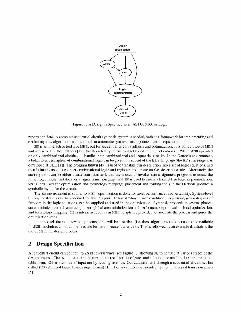
STG
ASTG
LogicImplementation
MappedCircuit
DesignSpecification
Figure 1: A Design is Specified as an ASTG, STG, or Logic
reported to date. A complete sequential circuit synthesis system is needed, both as a framework for implementing andevaluating new algorithms, and as a tool for automatic synthesis and optimization of sequential circuits.
SIS is an interactive tool like MISII, but for sequential circuit synthesis and optimization. It is built on top of MISIIand replaces it in the Octtools [12], the Berkeley synthesis tool set based on the Oct database. While MISII operatedon only combinational circuits, SIS handles both combinational and sequential circuits. In the Octtools environment,a behavioral description of combinational logic can be given in a subset of the BDS language (the BDS language wasdeveloped at DEC [1]). The program bdsyn [45] is used to translate this description into a set of logic equations, andthen bdnet is used to connect combinational logic and registers and create an Oct description file. Alternately, thestarting point can be either a state transition table and SIS is used to invoke state assignment programs to create theinitial logic implementation, or a signal transition graph and SIS is used to create a hazard-free logic implementation.SIS is then used for optimization and technology mapping; placement and routing tools in the Octtools produce asymbolic layout for the circuit.
The SIS environment is similar to MISII: optimization is done for area, performance, and testability. System-leveltiming constraints can be specified for the I/O pins. External “don’t care” conditions, expressing given degrees offreedom in the logic equations, can be supplied and used in the optimization. Synthesis proceeds in several phases:state minimization and state assignment, global area minimization and performance optimization, local optimization,and technology mapping. SIS is interactive, but as in MISII scripts are provided to automate the process and guide theoptimization steps.
In the sequel, the main new components of SIS will be described (i.e. those algorithms and operations not availablein MISII), including an input intermediate format for sequential circuits. This is followed by an example illustrating theuse of SIS in the design process.
2 Design SpecificationA sequential circuit can be input to SIS in several ways (see Figure 1), allowing SIS to be used at various stages of thedesign process. The two most common entry points are a net-list of gates and a finite-state machine in state-transition-table form. Other methods of input are by reading from the Oct database, and through a sequential circuit net-listcalled SLIF (Stanford Logic Interchange Format) [15]. For asynchronous circuits, the input is a signal transition graph[8].
2
2.1 Logic Implementation (Netlist)The net-list description is given in extended BLIF (Berkeley Logic Interchange Format) which consists of interconnectedsingle-output combinational gates and latches (see Appendix A for a description). The BLIF format, used in MISII,has been augmented to allow the specification of latches and controlling clocks. The latches are simple generic delayelements; in the technology-mapping phase they are mapped to actual latches in the library. Additionally, the BLIFformat accepts user-specified don’t care conditions. Designs can be described hierarchically although currently thehierarchy information is not retained in the internal data structure resulting in a flat netlist 1.
2.2 State Transition Graph (STG)A state transition table for a finite-state machine can be specified with the KISS [26] format, used extensively in stateassignment and state minimization programs. Each state is symbolic; the transition table indicates the next symbolicstate and output bit-vector given a current state and input bit-vector. External don’t care conditions are indicated bya missing transition (i.e., a present-state/input combination that has no specified next-state/output) or by a ‘-’ in anoutput bit (indicating that for that present-state/input combination that particular output can be either 0 or 1).
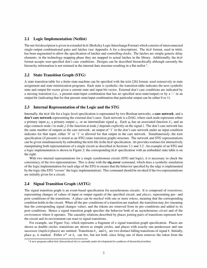
2.3 Internal Representation of the Logic and the STGInternally, the BLIF file for a logic-level specification is represented by two Boolean networks, a care network, and adon’t care network representing the external don’t cares. Each network is a DAG, where each node represents eithera primary input , a primary output , or an intermediate signal . Each has an associated function , and anedge connects node to node if the function at node depends explicitly on the signal . The don’t care network hasthe same number of outputs as the care network: an output of ‘1’ in the don’t care network under an input conditionindicates for that input, either ‘0’ or ‘1’ is allowed for that output in the care network. Simultaneously, the KISSspecification (if present) is stored as an STG (state transition graph) structure. The network and STG representationscan be given simultaneously by embedding the KISS file in the BLIF specification. SIS provides routines for interactivelymanipulating both representations of a single circuit as described in Sections 3.1 and 3.2. An example of an STG anda logic implementation is shown in Figure 2; the corresponding BLIF specification with an embedded state table is onthe right.
With two internal representations for a single synchronous circuit (STG and logic), it is necessary to check theconsistency of the two representations. This is done with the stg cover command, which does a symbolic simulationof the logic implementation for each edge of the STG to ensure that the behavior specified by the edge is implementedby the logic (the STG “covers” the logic implementation). This command should be invoked if the two representationsare initially given for a circuit.
2.4 Signal Transition Graph (ASTG)The signal transition graph is an event-based specification for asynchronous circuits. It is composed of transitions,representing changes of values of input or output signals of the specified circuit, and places, representing pre– andpost–conditions of the transitions. A place can be marked with one or more tokens, meaning that the correspondingcondition holds in the circuit. When all the pre–conditions of a transition are marked, the transitionmay fire (meaningthat the corresponding signal changes value), and the tokens are removed from its pre–conditions and added to itspost–conditions. Hence a signal transition graph specifies the behavior both of an asynchronous circuit and of theenvironment where it operates. The causality relations described by places joining pairs of transitions represent howthe circuit and its environment can react to signal transitions.
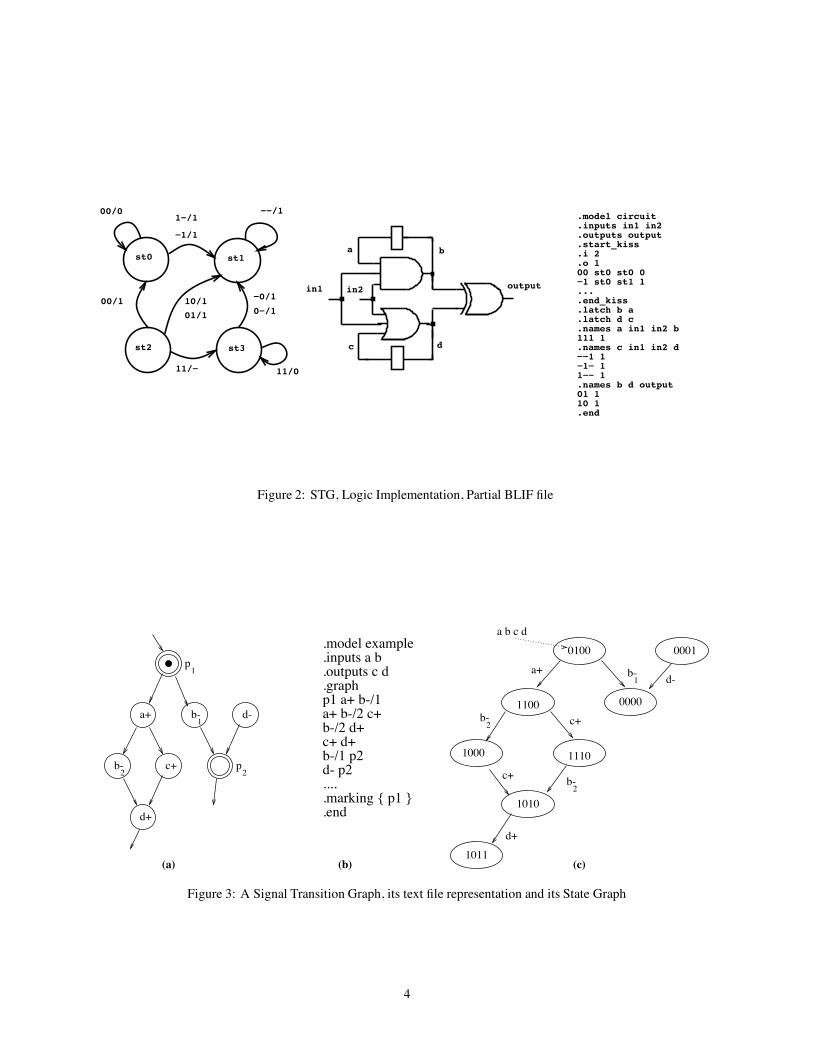
For example, see Figure 3(a), which represents a fragment of a signal transition graph specification. Places areshown as double circles, transitions are shown as simple circles, and places with exactly one predecessor and onesuccessor (implicit places) are omitted. Transitions 1 and 2 are two distinct falling transitions of signal . Initially,place 1 is marked. Either or 1 can fire, but not both, since firing one of them removes the token from the
1A new program called HSIS (hierarchical SIS) is currently under development for synthesis of hierarchical netlists.
3
st0 st1
st2 st3
00/01−/1
−−/1
00/1
−1/1
10/1
01/1
11/−
−0/1
0−/1
11/0
in1 in2 output
a b
c d
.model circuit
.inputs in1 in2
.outputs output
.start_kiss
.i 2
.o 100 st0 st0 0−1 st0 st1 1....end_kiss.latch b a.latch d c.names a in1 in2 b111 1.names c in1 in2 d−−1 1−1− 11−− 1.names b d output01 110 1.end
Figure 2: STG, Logic Implementation, Partial BLIF file
1b-
2b-
b-2
b-1
2b-
p2
p1
.model example
.inputs a b
.outputs c d
.graphp1 a+ b-/1a+ b-/2 c+b-/2 d+c+ d+b-/1 p2d- p2.....marking { p1 }.end
(c)(b)(a)
a b c d
0001
0000
1011
1010
11101000
0100
1100
d-
d+
c+
c+
a+
d-
d+
c+
a+
Figure 3: A Signal Transition Graph, its text file representation and its State Graph
4

predecessor of the other one ( and 1 are in conflict). If fires, signal changes value from 0 to 1. If 1fires, signal changes value from 1 to 0. Standard digital circuits are deterministic, so this kind of non-deterministicchoice between firing transition is allowed only for input signals (it allows a more abstract modeling of the circuitenvironment). If fires, it marks the implicit places between and 2 and between and . So causestransitions 2 and to be enabled ( and 2 are ordered). Transitions 2 and do not share a pre–condition, sothey can fire in any order ( 2 and are concurrent). When both have fired, becomes enabled, because both itspre–conditions are marked, and so on.
Note that the transitions in this fragment allow us to infer a value for each signal in each distinct marking of thesignal transition graph. For example, in the initial marking 0 (because its first transition, , will be rising), 1(because its first transition, either 1 or 2 , will be falling), and similarly 0 and 0. The value label attachedto each marking must be consistent across different firing sequences of the signal transition graph. For example, when2 is marked, the value for is always 0, independent of whether we fired or 1 (in the latter case the value foris the same as when 1 is marked, since no transition of fires between 1 and 2).
The existence of such a consistent labeling of each marking with signal values is the key for the correctness of asignal transition graph, together with three other properties:
liveness: for every transition, from every marking that can be reached from the initial one, we must be able toreach a marking where the transition is enabled (no deadlocks and no “operating cycles” that cannot be reachedfrom each other).
safeness: no more than one token can be present in a place in any reachable marking.
free-choice: if a place has more than one successor ( 1 in the example), then it must be the only predecessor ofthose transitions.
Furthermore a signal transition graph must be pure, i.e. no place can be both a predecessor and a successor of the sametransition, and place-simple, i.e. no two places can have exactly the same predecessors and successors.
A state machine (SM) is a signal transition graph where each transition has exactly one predecessor and onesuccessor place (no concurrency). A marked graph (MG) is a signal transition graph where each place has exactly onepredecessor and one successor transition (no choice). These two classes of signal transition graphs are useful becausesome synthesis algorithms can be used only, for example, on marked graphs, and some analysis algorithms decomposea general signal transition graph into state machine components or into marked graph components (see Section 3.3).
A signal transition graph can be represented as directed graph in a text file and read into SIS with the read astgcommand (an example is shown in Figure 3(b)). The first three lines (.model, .inputs and .outputs) have thesame meaning as in the BLIF format. In addition, the keyword .internal can be used to describe signals that arenot visible to the circuit environment, e.g. state signals. Everything after a “#” sign is treated as a comment.
Each line after .graph describes a set of graph edges. For example p1 a+ b-/1 describes the pair of edgesbetween 1 and and 1 respectively. The optional .marking line describes the set of initially marked places (ablank-separated list surrounded by braces). Implicit places, e.g. the place between and 2 , can be denoted in theinitial marking by writing its predecessor and successor transitions between angle brackets, e.g. <a+,b-/2>.
In addition to input, output and internal transitions, the signal transition graph model also allows dummy signals.Dummy signals, denoted by the keyword .dummy, just act as “placeholders” or “synchronizers” and do not representany actual circuit signal (so their transitions are not allowed to have a “+” or “-” sign). Dummy signals are very useful,for example, in transforming an asynchronous finite state machine into a signal transition graph by direct translation[9]. In this translation one explicit place represents each state, and it has one dummy transition for each output edge,followed by a set of transitions representing input signal changes2, followed by state signal changes, followed byoutput signal changes, followed by another dummy transition, followed by the place corresponding to the next state.Note that the input transitions must precede the state and output transitions in order to imply the correct deterministicbehavior, because the dummy transitions have no effect on the observable signals. In order for this direct translationto be possible, every finite state machine state must be entered with a single set of values of input and output signals,
2If more than one input signal changes value, this situation could not be represented, in general, by a free-choice signal transition graph withoutdummy transitions.
5
a b c’
a’ b’ c’
eps/4eps/3
eps/2eps/1
a’ b’ c’ + a b’ c’ + a’ b c’
(b)(a)
s3, 11s2, 01
s1, 00
a’ b’ ca b c’
d’ e’d e
d’ e’a+ b+
x0+
d+ e+
c+
p1
p2 p3
x0+ x1+
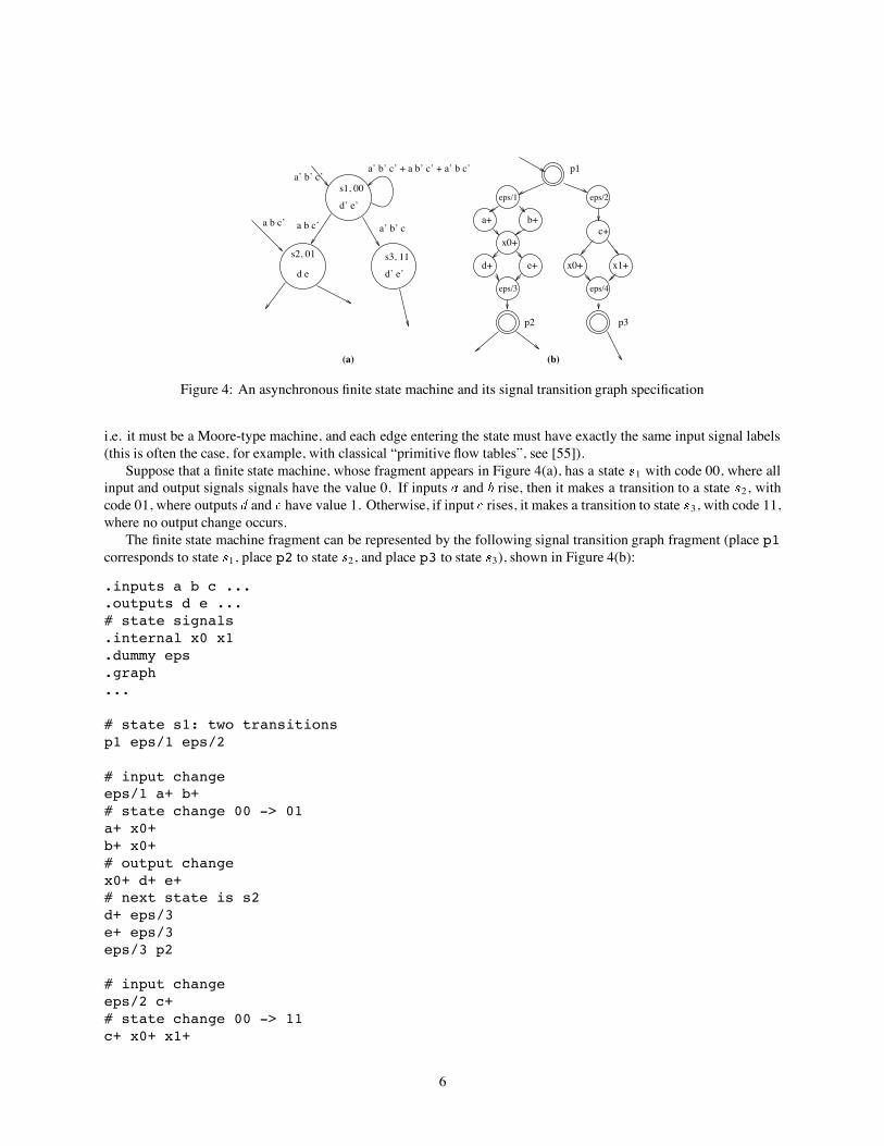
Figure 4: An asynchronous finite state machine and its signal transition graph specification
i.e. it must be a Moore-type machine, and each edge entering the state must have exactly the same input signal labels(this is often the case, for example, with classical “primitive flow tables”, see [55]).
Suppose that a finite state machine, whose fragment appears in Figure 4(a), has a state 1 with code 00, where allinput and output signals signals have the value 0. If inputs and rise, then it makes a transition to a state 2, withcode 01, where outputs and have value 1. Otherwise, if input rises, it makes a transition to state 3, with code 11,where no output change occurs.
The finite state machine fragment can be represented by the following signal transition graph fragment (place p1corresponds to state 1, place p2 to state 2, and place p3 to state 3), shown in Figure 4(b):
.inputs a b c ...
.outputs d e ...# state signals.internal x0 x1.dummy eps.graph...
# state s1: two transitionsp1 eps/1 eps/2
# input changeeps/1 a+ b+# state change 00 -> 01a+ x0+b+ x0+# output changex0+ d+ e+# next state is s2d+ eps/3e+ eps/3eps/3 p2
# input changeeps/2 c+# state change 00 -> 11c+ x0+ x1+
6

# no output change# next state is s3x0+ eps/4x1+ eps/4eps/4 p3
...
3 Part I: The SIS Synthesis and Optimization SystemSIS contains many new operations and algorithms, and it is the combination of these within a uniform frameworkthat allows the designer to explore a large design space. Some of these are enhancements to the combinationaltechniques previously employed inMISII. These include improvements to performance optimization (both restructuringand technology mapping), storage and use of external don’t cares, improved node minimization, and faster divisorextraction. In addition, new sequential techniques are included: an interface to state minimization and state assignmentprograms, retiming, sequential circuit optimization algorithms, finite-state machine verification, technology mappingfor sequential circuits, and synthesis of asynchronous designs.
3.1 STG Manipulations3.1.1 State Minimization
A state transition graph (STG) contains a collection of symbolic states and transitions between them. The degrees offreedom in this representation, or don’t cares, are either unspecified transitions or explicit output don’t cares. Thesedegrees of freedom, along with the notion that two states are equivalent if they produce equivalent output sequencesgiven equivalent input sequences, can be exploited to produce a machine with fewer states. This usually translates toa smaller logic implementation. Such a technique is called state minimization and has been studied extensively (e.g.[17, 31]). For completely specified machines the problem can be solved in polynomial time, while in the more generalcase of incompletely specified machines the problem is NP hard.
In SIS, state minimization has been implemented to allow the user to choose among various state minimizationprograms. No single state minimization algorithm has been integrated, but rather, the user can choose among stateminimization programs, distributed with SIS, or other programs that conform to an I/O specification designed for stateminimization programs. Programs that conform to the specification can be executed from the SIS shell. It has simplerequirements, e.g. that the program use the KISS format for input and output. For example, the user may invoke theSTAMINA [17] program, a heuristic state minimizer for incompletely specified machines distributedwith SIS, as follows:
sis> state_minimize stamina -s 1
In this case, STAMINA is used with its option ‘-s 1’ to perform state minimization on the current STG. When thecommand is completed, the original STG is replaced by the one computed by STAMINA with (possibly) fewer states.
3.1.2 State Assignment
State assignment provides themapping from an STG to a netlist. State assignment programs start with a state transitiontable and compute optimal binary codes for each symbolic state. These binary codes are used to create a logic-levelimplementation by substituting the binary codes for the symbolic states and creating a latch for each bit of the binarycode.
In SIS, the state assignment mechanism is similar to state minimization: the user is free to choose among stateassignment programs, provided those programs conform to a simple specification (in this case, the input is KISS andthe output is BLIF). A call to a state assignment program, such as
sis> state_assign nova -e ih
7

will perform optimal state assignment on the STG and return a corresponding logic implementation. Two stateassignment programs, JEDI[24] and NOVA [58] are distributed with SIS. JEDI is a general symbolic encoding program(i.e., for encoding both inputs and outputs) that can be used for the more specific state encoding problem; it is targetedfor multi-level implementations. NOVA is a state assignment program targeted for PLA-based finite-state machines; itproduces good results for multi-level implementations as well.
After state assignment there may be unused state codes, and from the KISS specification, unspecified transitionsand output don’t cares. These are external don’t cares for the resulting logic, and can be specified in the BLIF file thatis returned by the state assignment program, as is done with NOVA. These don’t care conditions will be stored andautomatically used in some subsequent optimization algorithms, such as full simplify (see Section 3.2.1).
3.1.3 STG Extraction
STG extraction is the inverse of state assignment. Given a logic-level implementation, the state transition graph canbe extracted from the logic for subsequent state minimization or state assignment. This provides a way of re-encodingthe machine for a possibly more efficient implementation. The STG extraction algorithm involves forward simulationand backtracking to find all states reachable from the initial state. Alternately, all 2 states can be extracted, whereis the number of latches. The resulting STG is completely specified because it is derived from the implementation
(which is completely specified by definition) and because the external don’t cares in the don’t care network are notused during the extraction. Thus to minimize the size of the STG the don’t cares should be given explicitly for theSTG representation. The stg extract operation should be used with caution as the STG may be too large to extract;the STG is in effect a two-level (symbolic) sum-of-products form.
3.2 Netlist ManipulationsSIS containsMISII and all the combinational optimization techniques therein. This includes the global area minimizationstrategy (iteratively extract and resubstitute common sub-expressions, eliminate the least useful factors), combinationalspeed-up techniques based on local restructuring, local optimization (node factoring and decomposition, two-level logicminimization using local don’t care conditions), and technology mapping for area or performance optimization. Someof these techniques have been improved significantly over the last available version ofMISII. In addition,new techniquesfor both combinational and sequential circuits have been introduced.
3.2.1 Combinational Optimization
Node Simplification
The logic function at a node is simplified in MISII using the simplify command which uses the two-level logicminimizer ESPRESSO [4]. The objective of a general two-level logic minimizer is to find a logic representation witha minimal number of implicants and literals while preserving the functionality. There are several approaches to thisproblem. In ESPRESSO, the offset is generated to determine whether a given cube is an implicant in the function. Theinput usually contains a cover for the onset and a cover for the don’t care set. A cover for the offset is generatedfrom the input using a complement algorithm based on the Unate Recursive Paradigm [4]. The number of cubes inthe offset can grow exponentially with the number of input variables; hence the offset generation could be quite timeconsuming. In the context of a multi-level network, node functions with many cubes in the offset and don’t care sethappen quite often, but the initial cover of the onset is usually small, and both the initial cover and the don’t care covermainly consist of primes.
To overcome the problem of generating huge offsets, a subset of the offset called the reduced offset is used [27].The reduced offset for a cube is never larger than the entire offset of the function and in practice has been found to bemuch smaller. The reduced offset can be used in the same way as the full offset for the expansion of a cube and noquality is lost. The use of the reduced offset speeds up the node simplification; however, if the size of don’t care setis too large, the computation of reduced offsets is not possible either. As a result, filters [40] must be introduced tokeep the don’t care size reasonably small. The filters are chosen heuristically with the goal that the quality of the nodesimplification is not reduced significantly.
8
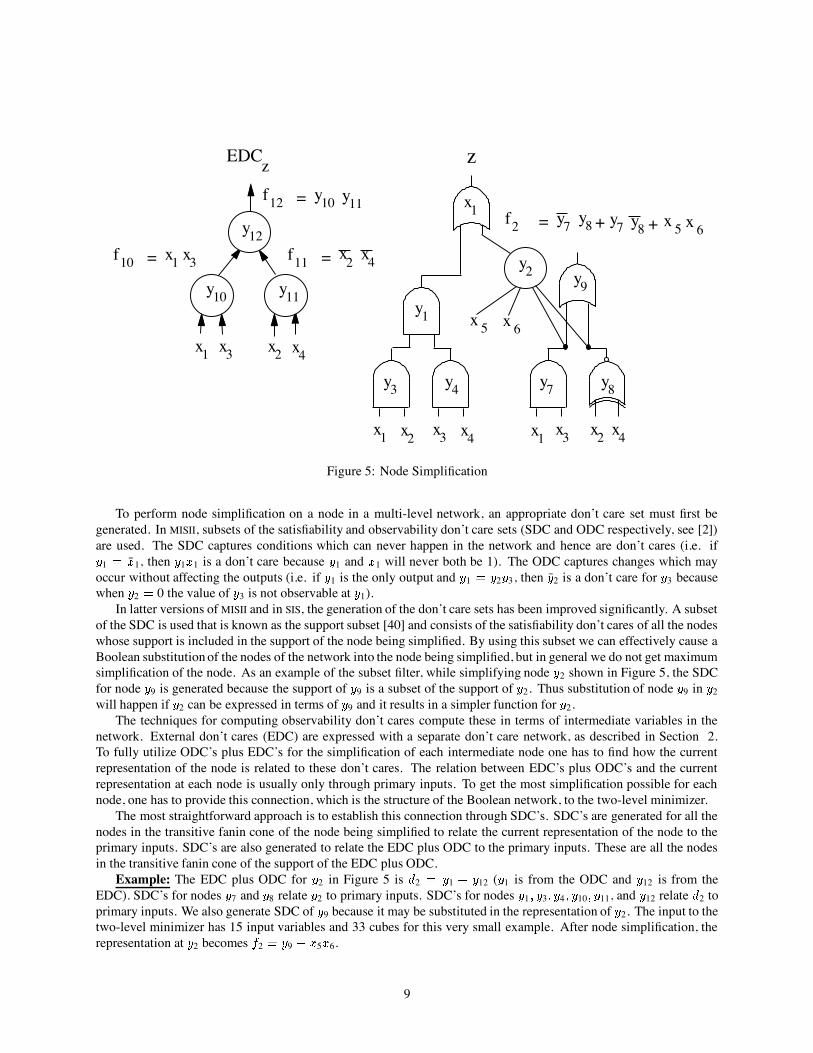
x1
EDC z
x3 x2 x4
y11y10
y12
z
y2 y9y1
x1
y3 y4 y7 y8
x1 x2 x3 x1x4 x3 x2 x4
f12 = y10 y11
f10 = x1 x3 f11 = x2 x4
f2 = y7 y8 + y7 y8 + 5x x 6
5x x 6
Figure 5: Node Simplification
To perform node simplification on a node in a multi-level network, an appropriate don’t care set must first begenerated. In MISII, subsets of the satisfiability and observability don’t care sets (SDC and ODC respectively, see [2])are used. The SDC captures conditions which can never happen in the network and hence are don’t cares (i.e. if1 ¯1, then 1 1 is a don’t care because 1 and 1 will never both be 1). The ODC captures changes which mayoccur without affecting the outputs (i.e. if 1 is the only output and 1 2 3, then ¯2 is a don’t care for 3 becausewhen 2 0 the value of 3 is not observable at 1).
In latter versions of MISII and in SIS, the generation of the don’t care sets has been improved significantly. A subsetof the SDC is used that is known as the support subset [40] and consists of the satisfiability don’t cares of all the nodeswhose support is included in the support of the node being simplified. By using this subset we can effectively cause aBoolean substitution of the nodes of the network into the node being simplified, but in general we do not get maximumsimplification of the node. As an example of the subset filter, while simplifying node 2 shown in Figure 5, the SDCfor node 9 is generated because the support of 9 is a subset of the support of 2. Thus substitution of node 9 in 2will happen if 2 can be expressed in terms of 9 and it results in a simpler function for 2.
The techniques for computing observability don’t cares compute these in terms of intermediate variables in thenetwork. External don’t cares (EDC) are expressed with a separate don’t care network, as described in Section 2.To fully utilize ODC’s plus EDC’s for the simplification of each intermediate node one has to find how the currentrepresentation of the node is related to these don’t cares. The relation between EDC’s plus ODC’s and the currentrepresentation at each node is usually only through primary inputs. To get the most simplification possible for eachnode, one has to provide this connection, which is the structure of the Boolean network, to the two-level minimizer.
The most straightforward approach is to establish this connection through SDC’s. SDC’s are generated for all thenodes in the transitive fanin cone of the node being simplified to relate the current representation of the node to theprimary inputs. SDC’s are also generated to relate the EDC plus ODC to the primary inputs. These are all the nodesin the transitive fanin cone of the support of the EDC plus ODC.Example: The EDC plus ODC for 2 in Figure 5 is 2 1 12 ( 1 is from the ODC and 12 is from the
EDC). SDC’s for nodes 7 and 8 relate 2 to primary inputs. SDC’s for nodes 1 3 4 10 11, and 12 relate 2 toprimary inputs. We also generate SDC of 9 because it may be substituted in the representation of 2. The input to thetwo-level minimizer has 15 input variables and 33 cubes for this very small example. After node simplification, therepresentation at 2 becomes 2 9 5 6.
9
It is obvious that this approach is not practical for networks with many levels; the size of satisfiability don’t careset grows very large in such cases and node simplification becomes computationally too expensive.
To reduce the size of the input to the two-level minimizer, several techniques are employed. External andobservability don’t cares are computed for each node using the techniques in [41]. The external don’t cares are onlyallowed in two-level form expressed directly in terms of primary inputs. A subset of the ODC called the CODC(compatible ODC) is computed for the simplification of each node. The compatible property ensures that the don’tcare sets on nodes can be used simultaneously with no need for re-computation after each node has been simplified.CODC’s are computed in terms of intermediate variables in the network. A collapsing and filtering procedure is usedto find a subset of the CODC which is in the transitive fanin cone of the node being simplified. A limited SDC isgenerated to use the CODC plus EDC in two-level form. However, EDC’s cannot be represented in two-level formin many cases because the number of cubes in the sum-of-products representation of EDC’s grows very large. Also,because of collapsing and filtering and the limited SDC generated the quality is reduced considerably compared towhat could be obtained using the full don’t care set.Example: The EDC plus ODC for 2 in Figure 5 in terms of primary inputs is 2 1 2 3 4 1 2 3 4. SDC’s
for nodes 7 8 and 9 must be generated. The input to the two-level minimizer has 9 input variables and 15 cubes.After node simplification, the representation at 2 becomes as before 2 9 5 6.
There is one final improvement to the don’t care set computation. Since each node has a local function :(assuming fanins), ideally one would like to express the external plus observability don’t cares of each node in
terms of its immediate fanins, not the primary inputs. These are minterms for which the value of can beeither 1 or 0 and the behavior of the Boolean network is unchanged. These local don’t cares are related to the EDC,ODC of , and SDC’s of the network and are as effective in node simplification as the full don’t care set.
Let be the node being simplified and : be the local function at this node in terms of its fanins1 . The local don’t care set is all the points in for which the value of is not important.To find , we first find the observability plus external don’t care set, , in terms of primary inputs. The care set
of in terms of primary inputs is . The local care set is computed by finding all combinations in reachablefrom . Any combination in that is not reachable from is in the local don’t care set .Example: The local don’t care for 2 is 2 7 8 (computed by effectively simulating the function 1 2 3 4
1 ¯2 3 ¯4 from the previous example). By examining the subset support, we determine that the SDC of 9 should beincluded. The input to the two-level minimizer has 5 inputs and 7 cubes. After node simplification, the representationat 2 becomes as before 2 9 5 6.
The command full simplify in SIS uses the satisfiability, observability, and external don’t cares to optimize eachnode in a multi-level network as described above. It first computes a set of external plus observability don’t cares foreach node: a depth-first traversal of the network starts at the outputswith the external don’t cares, and works backwardcomputing CODC’s for each node. At each intermediate node, the local don’t cares are computed in terms of faninsof the node being simplified by an image computation which uses BDD’s. This don’t care set is augmented with somelocal SDC’s, and minimized with the two-level minimizer ESPRESSO [4]. Results for full simplify are reported in [42].This command should not be applied to networks where the BDD’s become too large; there is a built-inmechanism tohalt the computation if this occurs.
Kernel and Cube Extraction
An important step in network optimization is extracting new nodes representing logic functions that are factors ofother nodes. We do not know of any Boolean decomposition technique that performs well and is not computationallyexpensive; therefore we use algebraic techniques. The basic idea is to look for expressions that are observed manytimes in the nodes of the network and extract such expressions. The extracted expression is implemented only onceand the output of that node replaces the expression in any other node in the network where the expression appears.This technique is dependent on the sum-of-products representation at each node in the network and therefore a slightchange at a node can cause a large change in the final result, for better or for worse.
The current algebraic techniques in MISII are based on kernels [3]. The kernels of a logic expression are definedas
10
where c is a cube, g has at least two cubes and is the result of algebraic division of by , and there is no commonliteral among all the cubes in (i.e. is cube free). This set is smaller than the set of all algebraic divisors of thenodes in the network, therefore it can be computed much faster and is almost as effective. One problem encounteredwith this in practice is that the number kernels of a logic expression is exponentially larger than the number of cubesappearing in that expression. Furthermore, after a kernel is extracted, there is no easy way of updating other kernels,so kernel extraction is usually repeated. Once all kernels are extracted the largest intersection that divides most nodesin the network is sought. There is no notion of the complement of a kernel being used at this stage. After kernels areextracted, one looks for the best single cube divisors and extracts such cubes. The kernels and cubes are sought only innormal form. Later on, Boolean or algebraic resubstitution can affect division by the complement as well. Extractionof multi-cube divisors and common cubes from a network in MISII is done with the gkx and gcx commands.
A more recent algebraic technique extracts only two-cube divisors and two-literal single-cube divisors both innormal and complement form [57]. This approach has several advantages in terms of computation time while thequality of the final result is as good as kernel-based approaches according to [57] as well as our experimental results. Itis shown that the total number of double-cube divisors and two-literal single-cube divisors is polynomial in the numberof cubes appearing in the expression. Also, this set is created once, and can be efficiently updated when a divisor isextracted. Additionally, one looks for both normal and complement form of a divisor in all the nodes in the networkso in choosing the best divisor a better evaluation can be made based on the usefulness of the divisor as well as itscomplement. There is also no need for algebraic resubstitution once divisors are extracted.
The algorithmworks as follows. First all two-cube divisors and two-literal single-cube divisors are recognized andput in a list. A weight is associated with each divisor which measures how many literals are saved if that expression isextracted. This weight includes the usefulness of the complement in the cases where the complements are single cubesor other two-cube divisors. Common cube divisors are also evaluated at the same time so that "kernel" extraction and"cube" extraction are nicely interleaved by this process. The divisor with highest weight is extracted greedily. Allother divisors and their weights are updated and the whole process is repeated until no more divisors can be extracted.This technique has been implemented in SIS and is called fast extract or fx. Generally, it should replace the MISIIcommands gkx and gcx since its quality is comparable but its speed in many cases is substantially higher [43].
One shortcoming of this approach is that the size of each divisor is limited to no more than two cubes. However,large nodes are effectively extracted by the combined process of fast extract and elimination. Elimination is used toincrease the size of some divisors and remove others that are not effective.
Test Pattern Generation and Redundancy Removal
A very efficient automatic test pattern generation algorithm for combinational logic has been implemented in SIS.First, fault collapsing is performed across simple gates; both fault equivalence and fault dominance are used to reducethe fault list. Random test generation is done using parallel fault simulation. After the random patterns have beensimulated, the algorithm performs a deterministic search to find tests for the remaining faults. This part is based onthe algorithm reported in [19]: a set of equations is written to express the difference between the good and faultycircuits for a particular fault and Boolean satisfiability is used to find a satisfying assignment for these equations.The implementation of the algorithm in SIS has been substantially improved for speed. While the single-stuck-faulttest pattern generation problem is NP-complete, this implementation has been able to produce 100% stuck-at faultcoverage in all test cases available to us. The command atpg file in SIS produces a set of test vectors in the file file.The redundancy removal command red removal is based on these techniques and iteratively removes all redundantfaults.
Technology Mapping
MISII uses a tree-covering algorithm to map arbitrary complex logic gates into gates specified in a technologylibrary [39]. (The technology library is given in genlib format, which is described in Appendix B.) This is doneby decomposing the logic to be mapped into a network of 2-input NAND gates and inverters. This network is then“covered” by patterns that represent the possible choices of gates in the library. During the covering stage the areaor the delay of the circuit is used as an optimization criterion. This has been successful for area minimization butineffective for performance optimization because the load at the output of gates is not considered when selecting
11
gates and no optimization is provided for signals that are distributed to several other gates. Recent refinements havesignificantly improved it for performance optimization, as reported in [54]; tree covering has been extended to takeload values into account accurately. In addition, efficient heuristic fanout optimization algorithms, reported in [51],have been extended and implemented. They are also used during tree covering to estimate delay at multiple fanoutpoints; this enables the algorithm to make better decisions in successive mapping passes over the circuit.
In addition to the technology mapping for delay another command that inserts buffers in the circuit to reducedelay, is provided. The command buffer opt [47] takes as input a circuit mapped for minimum area (map -m 0) andinserts buffers to improve circuit performance. This command is subsumed by the map -m 1 -A command whichin addition to adding buffers also makes selections of the gates to implement the logic functions. However, it doesprovide a design whose area and delay are intermediate to the minimum-area and minimum-delay mapped circuits.
Restructuring for Performance
The delay of the circuit is determined by the multi-level structure of the logic as well as the choice of gates usedto implement the functions. There are two algorithms that address the restructuring of the logic to improve the delay.These are speed up [48] and reduce depth [52].
The speed up command operates on a decomposition of the network in terms of simple gates (2-input NAND gatesand inverters). This description is the same as that used by technologymapping. The speed up command tries to reducethe depth of the decomposed circuit with the intuition that a small depth representation will result in a smaller delay.The restructuring is performed by collapsing sections along the long paths and resynthesizing them for better timingcharacteristics [48]. Following the restructuring the circuit ismapped forminimumdelay. The recommended use of thespeed up command is to run the following on an area-optimized circuit: gd *; eliminate -1; speed up;map -m 1 -A.
The reduce depth command takes a different approach to technology-independent network restructuring forperformance optimization [52]. The idea is to uniformly reduce the depth of the circuit. It does this by first clusteringnodes according to some criteria and then collapsing each cluster into a single node. The clusters are formed as follows:a maximum cluster size is computed, and the algorithmfinds a clustering that respects this size limit and minimizes thenumber of levels in the network after collapsing the clusters. The cluster size limit can be controlled by the user. Theclustering and collapsing results in a large area increase. Hence, it is important to follow the clusteringwith constrainedarea-optimization techniques that will not increase the circuit depth. This is done by using the simplify -l andfx -l commands. The -l option ensures that depth of the circuit will not increase. A special script script.delaythat uses the reduce depth command is provided for automating synthesis for performance optimization.
3.2.2 Sequential Optimization
All of the combinational techniques described above can be applied to the combinational blocks between registerboundaries in a sequential circuit. Further improvements can be made by allowing the registers to move and byperforming optimizations across register boundaries. Some of these techniques are described in the following section,including retiming, retiming and resynthesis, and retiming don’t cares. Some extensions are required for the technologymapping algorithms to work on sequential circuits. Finally, sequential don’t cares based on unreachable states can becomputed and used during node minimization.
Retiming
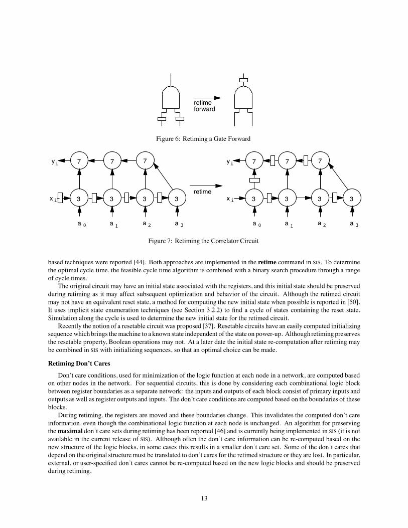
Retiming [22] is an algorithm that moves registers across logic gates either to minimize cycle time, minimize thenumber of registers, or minimize the number of registers subject to a cycle-time constraint. It operates on synchronousedge-triggered designs. A particular gate is retimed forward by moving registers from each of its fanins to each of itsfanouts (see Figure 6). The sequential I/O behavior of the circuit is maintained. An example of retiming for minimumcycle time taken from [21] is shown in Figure 7. This example represents a correlator circuit, which takes a streamof bits and compares it with a pattern 0 1 2 3. The delays of each of the components are given (delay = 3 for acomparator, 7 for an adder). For this circuit, the cycle time is reduced from 24 to 13.
The original algorithm[23] was based on a mixed-integer linear programming formulation for determiningwhethera particular cycle time is feasible; if so, the correct register positions are determined. Later, more efficient relaxation-
12
retimeforward
Figure 6: Retiming a Gate Forward
3 3 3 3
a 10 2 3a a a
7 7 7
x
y
i
i
3 3 3 3
a 10 2 3a a a
7 7 7
x
y
i
i
retime
Figure 7: Retiming the Correlator Circuit
based techniques were reported [44]. Both approaches are implemented in the retime command in SIS. To determinethe optimal cycle time, the feasible cycle time algorithm is combined with a binary search procedure through a rangeof cycle times.
The original circuit may have an initial state associated with the registers, and this initial state should be preservedduring retiming as it may affect subsequent optimization and behavior of the circuit. Although the retimed circuitmay not have an equivalent reset state, a method for computing the new initial state when possible is reported in [50].It uses implicit state enumeration techniques (see Section 3.2.2) to find a cycle of states containing the reset state.Simulation along the cycle is used to determine the new initial state for the retimed circuit.
Recently the notion of a resetable circuit was proposed [37]. Resetable circuits have an easily computed initializingsequence which brings themachine to a known state independent of the state on power-up. Although retiming preservesthe resetable property, Boolean operations may not. At a later date the initial state re-computation after retiming maybe combined in SIS with initializing sequences, so that an optimal choice can be made.
Retiming Don’t Cares
Don’t care conditions, used for minimization of the logic function at each node in a network, are computed basedon other nodes in the network. For sequential circuits, this is done by considering each combinational logic blockbetween register boundaries as a separate network: the inputs and outputs of each block consist of primary inputs andoutputs as well as register outputs and inputs. The don’t care conditions are computed based on the boundaries of theseblocks.
During retiming, the registers are moved and these boundaries change. This invalidates the computed don’t careinformation, even though the combinational logic function at each node is unchanged. An algorithm for preservingthemaximal don’t care sets during retiming has been reported [46] and is currently being implemented in SIS (it is notavailable in the current release of SIS). Although often the don’t care information can be re-computed based on thenew structure of the logic blocks, in some cases this results in a smaller don’t care set. Some of the don’t cares thatdepend on the original structuremust be translated to don’t cares for the retimed structure or they are lost. In particular,external, or user-specified don’t cares cannot be re-computed based on the new logic blocks and should be preservedduring retiming.
13

c
a
b
d
x
y
g1
g2
(a) Sequential Circuit (b) Peripherally Retime
c
a
b
d
x
y
g1
g2
−1
c
a
b
d
x
y
g2
−1
(c) Resynthesize
c
a
b
d
x
y
g2
(d) Retime
Figure 8: Retiming and Resynthesis Example
As a by-product of the investigation on retiming don’t cares, an algorithm was developed for propagating don’tcare conditions forward in a network. That is, given the don’t cares for the inputs of a node, an appropriate don’tcare function is computed for the output of the node. Techniques for propagating don’t cares backward have alreadybeen developed in the work on ODC’s [42]. Together, the forward and backward propagation algorithms can be usedto propagate don’t care conditions completely throughout a network, regardless of where these don’t cares originate.
Retiming and Resynthesis
Retiming finds optimal register positionswithout altering the combinational logic functions at each node. Standardcombinational techniques optimize a logic network, but given a sequential circuit, the optimization is limited to eachcombinational block: interactions between signals across register boundaries are not exploited.
These two techniques are combined in the retiming and resynthesis algorithm [28]. The first step is to identify thelargest subcircuits that can be peripherally retimed, i.e. that can be retimed in such a way as to move all the registers tothe boundaries of the subcircuit. Peripheral retiming is an extended notion of retiming where “negative” latches at theboundary are allowed (time is borrowed from the environment) as long as they can be retimed away after resynthesis.After peripheral retiming, standard combinational techniques are used to minimize the interior logic. Finally, theregisters are retimed back into the circuit to minimize cycle time or the number of registers used. An example of thisprocedure is shown in Figure 8. In the example, pure combinational optimization would not yield any improvement,and standard retiming as it was first described cannot be applied to the circuit. It is only by combining peripheralretiming, which allows negative registers, and resynthesis that the improvement is obtained.
This algorithm has been successful in performance optimization of pipelined circuits [29]. Experiments with areaminimization are ongoing, but it is expected that good results will be obtained only when the latest combinationaloptimization techniques, which use a larger set of observability don’t cares, are employed. In particular, those that
14
use a maximal observability don’t care set can exploit the signal dependencies exposed during peripheral retiming.Retiming and resynthesis will be implemented in SIS after further investigation and experimentation.
Technology Mapping
The strategy of representing feedback lines by latches preserves the acyclic nature of the circuit representationand allows the combinational technology mapping algorithms to be easily extended to sequential mapping [33]. Thesame tree-covering algorithm [39] is used but the pattern matching procedure is extended to accommodate sequentialelements. The pattern matching relies no longer on just the network topology but also on the type of library elementand on the location of latch input and output pins. By choosing to treat the problem of selecting a clocking scheme(single-phase synchronous, multi-phase synchronous or even asynchronous) and clocking parameters as a higher levelissue, the output of sequential technology mapping can be controlled by simply restricting the types of sequentialelements allowed in the technology library. This approach can handle complex latches which are either synchronousor asynchronous, but not both (for example, synchronous latches with asynchronous set/reset) 3.
Implicit State Enumeration Techniques
Recently, methods for implicitly enumerating the states in a finite-state machine have been reported and can beused to explore the state space in very large examples [10, 53]. Such techniques employ a breadth-first traversal ofsets of states of a machine. Beginning with an initial state set, all the states reachable in one transition from that setare computed simultaneously, then all the states reachable in two transitions, etc. Efficient implementation of thistechnique requires careful computation of the product of the transition relation (present-state/next-state relation) andthe current set of states. This can be done either by reducing the size of the resulting function during computation byeliminating variables appropriately [53], or by using a divide and conquer approach [10]. Each function is efficientlyimplemented and manipulated using BDDs [6].
These techniques are useful for generating sequential don’t care conditions. The reachable state set is computedwith implicit techniques; the complement of this set represents the unreachable states. These are don’t care conditionsexpressed in terms of the registers in the circuit. In SIS the command extract seq dc extracts the unreachable statesand stores them as external don’t cares. Subsequent calls to full simplify (see Section 3.2.1) exploit these don’t cares.
Implicit state enumeration techniques are also useful for verification. The equivalence of two finite-state machines(logic-level implementations) can be verified by computing the reachable states for the product machine. The twomachines may have different state encodings. At each iteration, the states reached are checked for equivalent outputfunctions. The verify fsm command in SIS has verified machines with more than 1068 states [53].
3.3 Signal Transition Graph ManipulationsThe design input to SIS need not be a synchronous specification. An asynchronous specification can be given as asignal transition graph. In this section, algorithms are outlined for the synthesis of hazard-free circuits under differentdelay models from signal transition graphs.
If a signal transition graph is correct (live, safe, free choice and with a consistent labeling), then it can beautomatically synthesized if it satisfies another condition:
complete state coding: whenever twomarkings have the same label, then theymust enable the same set of outputtransitions.
The synthesis is performed by exhaustive simulation of all reachable markings. This produces a state graph,where each marking is associated with a state, and each edge, representing a transition firing, joins the correspondingpredecessor and successor markings. For example, in Figure 3(c) the state graph fragment corresponding to Figure 3(a)is shown, where the state labeled 0100 corresponds to 1 being marked.
If the signal transition graph is correct and has complete state coding, then we can derive from the state graph animplied value for each output signal in each state as follows. For every state , for every output signal , the impliedvalue of in is:
3Such latches cannot be represented by a combinational network feeding a latch element; the require some additional logic at the latch output.This introduces cyclic dependency to the cost function, and the tree-covering can no longer be solved by a dynamic programming algorithm.
15
the value of in the label of if no transition for is enabled in the marking corresponding to . For example,in state 0100, corresponding to 1 being marked, no transition for is enabled, so the implied value of is 0.
otherwise, the complement of that value. For example, in state 0100 transition 2 is enabled, so the impliedvalue of in 0100 is 0.
A combinational function, computing the implied value for each input label (minterm) obviously implements therequired behavior of each output signal. This straightforward implementation, though, can still exhibit hazards (i.e.temporary deviations from the expected values, due to the non-zero delays of gates and wires in a combinationalcircuit). SIS provides an implementation of the algorithms described in [32] and [20] to produce hazard-free circuitsunder the unbounded gate-delaymodel and the bounded wire-delay model respectively.
The commands that operate on a signal transition graph and produce an asynchronous circuit implementation of itcan be roughly classified as analysis and synthesis commands.
Analysis commands
astg current prints some information on the current signal transition graph.
astg marking prints the current marking, if any, of the signal transition graph (it is useful if the marking wasobtained automatically by SIS , since this is an expensive computation).
astg print sg prints the state graph obtained during the synthesis process (mainly useful for debuggingpurposes).
astg print stat prints a brief summary of the signal transition graph and state graph characteristics.
Synthesis commands
astg syn synthesizes a hazard-free circuit using the unbounded gate-delaymodel. It eliminates hazards from theinitial circuit, produced from the implied values as described above, by adding redundant gates and/or addinginput connections to some gates, as described in [32]. This command (as well as astg to f) can compute theinitial marking if it is not explicitly given.
astg to f synthesizes a circuit (like astg syn), but in addition it analyzes and stores its potential hazards using theboundedwire-delaymodel4. Those hazards can be eliminated, after a constrained logic synthesis and technologymapping, by the astg slow command.
astg slow inserts delays, as described in [20], in order to produce a hazard-free circuit in a specific implementationtechnology. Note that this step can take advantage of the knowledge aboutminimum delays in the environment5.These delays can either be given as a single lower bound, with the -d option, or in a file, with the -f option.Each line in this environment delay file contains a pair of signals and a pair of numbers, and represents theminimum guaranteed lower bound on the delay between a transition on the first signal and a rising/fallingtransition respectively on the second signal.In order to do worst-case hazard analysis, astg slow also provides a rudimentary mechanism to describe gateswith upper and lower bounds on the delay, using the -m option. This option specifies a multiplicative factorto obtain the minimum delay of each gate, given its maximum delay as specified by the gate library used fortechnology mapping.Note that the astg to f and astg slow commands require that only algebraic operations during logic synthesis inorder to guarantee hazard-free synthesis. Namely only the sweep, fx, gkx, gcx, resub, eliminate, decomp andmap commands can be used. Other commands such as simplify and full simplifymay re-introduce hazards.
4Note that a circuit that does not have hazards with the unbounded gate delay model, where all wire delays are assumed to be zero, can exhibithazards with the bounded wire-delay model. The designer should use the delay model that best suits the underlying implementation technology(see [7]).
5By default the environment is assumed to respond instantaneously, since this represents a pessimistic worst-case assumption for hazard analysis.
16

TLU Synthesisxl ao cube-packing on an infeasible networkxl k decomp apply Roth-Karp decompositionxl split modified kernel extractionxl imp apply different decomposition schemes and pick the bestxl absorb reduce infeasibility of the networkxl cover use binate covering to minimize number of blocksxl partition minimize number of blocks by collapsing nodes into immediate fanoutsxl part coll initial mapping and partial collapse on the networkxl merge identify function-pairs to be placed on the same CLBxl decomp two cube-packing targeted for two-output CLB’sxl rl reduce number of levelsxl nodevalue print infeasible nodes
MB Synthesisact map block count minimization for act1 and act architectures
Table 1: PGA Synthesis Commands in SIS
astg contract, given a specific output signal for which logic needs to be synthesized, removes from the signaltransition graph all the signals that are not directly required as inputs of the logic implementing . Note thatcontraction is guaranteed to yield a contracted signal transition graph with complete state coding only if theoriginal signal transition graph was a marked graph.
astg lockgraph, given a correct signal transition graph without complete state coding, uses the algorithmdescribed in [56] to produce a signal transition graph with less concurrency but complete state coding (so that itcan be synthesized). Note that this technique works successfully only for marked graphs.
astg persist ensures that the signal transition graph is persistent, i.e. no signal that enables a transition canchange value before that transition has fired (this property ensures a somewhat simpler implementation, at thecost of a loss in concurrency). Note that this command works successfully only for marked graphs.
astg to stg produces a state transition graph representation that describes a behavior equivalent to the signaltransition graph. It can be used, for example, to compare a synchronous and an asynchronous implementationof (roughly) the same specification.
3.4 Logic Synthesis for Programmable Gate Arrays (PGA’s)Synthesizing circuits targeted for particular PGA architectures requires new architecture-specific algorithms. Anumber of these have been implemented in latter versions of MISII, and are being improved and enhanced in SIS. Thesealgorithms are described briefly in this section. A summary of the commands in SIS for PGA synthesis are given inTable 1.
The basic PGA architectures share a common feature: repeated arrays of identical logic blocks. A logic block (orbasic block) is a versatile configuration of logic elements that can be programmed by the user. There are two maincategories of block structures, namely Table-Look-Up (TLU) and Multiplexor-Based (MB); the resulting architecturesare called the TLU and theMB architectures respectively. A basic block of a TLU architecture (also called configurablelogic block or CLB) implements any function having up to inputs, 2. For a given TLU architecture, is afixed number. A typical example is the Xilinx architecture [18], in which 5. In MB architectures, the basic blockis a configuration of multiplexors [13]. In SIS, combinational circuits can be synthesized for both these architectures.Area minimization for both architectures and delay minimization for TLU architectures are supported. We are workingon extending the capabilities to handle sequential circuits.
17

The algorithms and the corresponding commands that implement them in SIS are described next. For completedetails of the algorithms, the reader may refer to [34, 35, 36].
3.4.1 Synthesis for TLU architectures
If a function has at most inputs, we know it can be realized with one block. We call such a function -feasible.Otherwise, it is -infeasible. A network is -feasible if the function at each node of the network is -feasible. Letus first address the problem of minimizing the number of basic blocks used to implement a network. We assume thatthe technology-independent optimizations have been already applied on the given network description.
In order to realize an infeasible network using the basic blocks, we have to first make infeasible nodes feasible.After obtaining a feasible network, we have to minimize the number of blocks used. These two subproblems aredescribed next.
Making an infeasible node feasible
Decomposition is a way of obtaining smaller nodes from a large node. We use decomposition to obtain a set of-feasible nodes for an infeasible node function. The following is a summary of various decomposition commands
for TLU architectures that are in SIS:xl ao cube-packing on an infeasible networkxl k decomp apply Roth-Karp decompositionxl split modified kernel extractionxl imp apply different decomposition schemes and pick the bestCube-packing [14] used in xl ao treats the cubes (product-terms) of the function as items. The size of each cube
is the number of literals in it. Each logic block is a bin with capacity . The decomposition problem can then be seenas that of packing the cubes into a minimum number of bins.xl k decomp uses classical Roth-Karp decomposition [38] to decompose an infeasible node into -feasible nodes.
A set (called the bound set) of cardinality is chosen from the inputs of the infeasible function . The rest of theinputs form the free set . Then the Roth-Karp technique decomposes as follows:
1 2 1
where 1 2 are -feasible functions. If , is infeasible and needs to be decomposed further.To get the best possible decomposition, all possible choices of bound sets have to be tried. With options -e and -f,all bound sets of a node are tried and the one resulting in the minimum number of nodes is selected.xl split extracts kernels from an infeasible node. This procedure is recursively applied on the kernel and the node,
until either they become -feasible or no more kernels can be extracted, in which case a simple and-or decompositionis performed.xl imp tries to get the best possible decomposition for the network. It applies a set of decomposition techniques
on each infeasible node of the network. These techniques include cube-packing on the sum-of-products form of ,cube-packing on the factored form of , Roth-Karp decomposition, and kernel extraction. The best decompositionresult - the one which has a minimum number of -feasible nodes - is selected.
One command which does not necessarily generate an -feasible network, but reduces the infeasibilityof a networkis xl absorb. Infeasibility of a network is measured as the sum of the number of fanins of the infeasible nodes. Thecommand xl absorbmoves the fanins of the infeasible nodes to feasible nodes so as to decrease the infeasibility of thenetwork. Roth-Karp decomposition is used to determine if a fanin of a node could be made to fan in to another node.
Block Count Minimization
After decomposition, an -feasible network is obtained and may be mapped directly onto the basic blocks.However, it may be possible to collapse some nodes into their fanouts while retaining feasibility. The followingcommands in SIS do the block count minimization:
xl cover use binate coveringxl partition collapse nodes into immediate fanouts
18
xl cover enumerates all sets of nodes which can be realized as a single block. Each such set is called a supernode.The enumeration is done using the maximum flow algorithm repeatedly. A smallest subset of supernodes that satisfythe following three constraints is selected:
1. each node of the network should be included in at least one supernode in ,
2. each input to a supernode in should either be an output of another supernode in , or an external input to thenetwork, and
3. each output of the network should be an output of some supernode in .
This is a binate covering formulation [39]. Mathony’s algorithm [30] is used to solve this formulation. For largenetworks, this algorithm is computationally intensive and several heuristics for fast approximate solutions are used(option -h).xl partition tries to reduce the number of nodes by collapsing nodes into their immediate fanouts. It also takes into
account extra nets created. It collapses a node into its fanout only if the resulting fanout is -feasible. It associates acost with each (node, fanout) pair which reflects the extra nets created if node is collapsed into the fanout. It then selectspairs with lowest costs and collapses them. With-t option, a node is considered for collapsing into all the fanouts, andis collapsed if all the fanouts remain -feasible after collapsing. The node is then deleted from the network. Furtheroptimization results by considering the technique of moving of fanins (using -m option). This technique is applied asfollows. Before considering the collapse of node into its fanout(s), we check if any fanin of could be movedto - another fanin of . This increases the chances of being collapsed into its fanout(s). Moreover, it may laterenable some other fanin of to be collapsed into .
Overall Algorithm
We first apply technology-independent optimization on the given network. Each infeasible node of this network ismapped as follows. We first decompose it into an -feasible subnetwork using the techniques discussed above. Theblock count minimization is then applied on this subnetwork. Applying decomposition and block count minimizationnode-by-node gives better results than first applying decomposition on the entire network and then using block countminimization. The reason is that the exact block count minimization on the full network is computationally intensive,and hence is run only in heuristic mode.
The node-by-node mapping paradigm does not exploit structural relationship between the nodes of the network.This is achieved in command xl part coll (for partial collapse) by collapsing each node into its fanouts, remappingthe fanouts, and computing the gain from this collapse. A greedy approach is employed - the collapse is accepted if itresults in a gain.
Next we apply a heuristic block count minimization on the entire network (for example xl cover -h 3).For good results, the following script may be used:
xl part coll -m -g 2xl coll ckxl partition -msimplifyxl impxl partition -txl cover -e 30 -u 200xl coll ck -k
For very fast results, the following script may be used:xl aoxl partition -tm
xl coll ck collapses a feasible network if the number of primary inputs is small (specified by -c option), appliesRoth-Karp decomposition and cofactoring schemes, picks the best result and compares with the original network
19

(before collapsing). If the number of nodes is smaller, accepts the better decomposition. It does nothing if = 2. If-k option is specified, Roth-Karp decomposition is not applied; only cofactoring is used.
Note that in all the commands, the default value of is 5. It may be changed by specifying -n option to eachcommand. Intermediate points in the quality-time trade-off curve may be obtained by suitably modifying the scripts.
One useful command not described above is xl nodevalue -v support. It prints nodes that have at least supportfanins. This command is used to make sure that a feasible network has indeed been obtained. For example, if 5,use xl nodevalue -v 6.
Handling Two Outputs
There are special features in some TLU architectures. For example, in the Xilinx architecture, a CLB mayimplement one function of at most 5 inputs, or two functions if both of them have at most 4 inputs each and the totalnumber of inputs is at most 5 (in which case they are called mergeable). The problem is to minimize the number oftwo-output CLB’s used for a given circuit description. SIS has two special commands for handling two-output CLB’s:
xl merge identify function-pairs to be placed on the same blockxl decomp two cube-packing targeted for two-output CLB’sThe approach currently followed in SIS is to minimize first the number of single-output blocks using the script(s)
described above and then use xl merge as a post-processing step to place maximum number of mergeable function-pairs in one CLB each. This reduces to the following problem: “Given a feasible network, find the largest set ofdisjoint pairs of mergeable functions.” We have shown that this problem can be formulated as themaximum cardinalitymatching problem in a related graph. An exact solution can be generated using lindo, an integer linear programmingpackage. If lindo is not found in the path, xl merge switches to a heuristic to solve the matching problem.
A different approach that sometimes gives better results is the following. First obtain a 4-feasible network (byrunning any one of the above scripts with -n 4) and then use xl merge without -F option. Since there are no nodeswith 5 inputs, all nodes can potentially pair with other nodes. As a result the number of matches is higher. When-F option is not used, xl merge first finds maximum number of mergeable function pairs and then applies blockminimization on the subnetwork consisting of unmatched nodes of the network. This sometimes results in furthersavings. We recommend that the user should use scripts for both 4-feasible and 5-feasible, apply xl merge and pickthe network that uses lower number of CLB’s.
The command xl decomp two does decomposition of the network targeted for two-outputCLB’s. It is a modifica-tion of the cube-packing approach. However, it does not guarantee a feasible network; other decomposition commandsshould be run afterwards to ensure feasibility.
Timing Optimization
xl rl performs delay optimizations during logic synthesis. Given a feasible network (preferably generated byspeed up), xl rl reduces the number of levels of TLU blocks used in the network. Then any block count minimizationcommand (e.g. xl cover, xl partition) can be applied to reduce the number of blocks without increasing the numberof levels. The details of the complete algorithm may be found in [36].
3.4.2 Synthesis for MB architectures
We have implemented synthesis algorithms for Actel’s act1 architecture (Figure 9). The command is called act map.The architecture act (that is, act1 with the OR gate removed) is also supported. No library needs to be read.
The outline of the algorithm [34] is as follows: first, for each node of the network a BDD (ordered or unordered) isconstructed. The basic block of the architecture is represented with pattern graphs. The problem of covering the BDDwith minimum number of pattern graphs is solved by first decomposing the BDD into trees and then mapping eachtree onto the pattern-graphs using a dynamic programming algorithm. The overall algorithm is very similar to the onefor TLU architecture. After initial mapping, an iterative improvement phase of partial collapse, decomposition andquick phase is entered. Quick phase decides if it is better to implement a node in the complement form. The user mayspecify number of iterations, limits on number of fanins of nodes for collapsing or decomposition. A bdnet-like filemay be generated in which case the mapped network consists of nodes that are implemented by one basic block each.
20

MUX1
MUX2
MUX3
OR
act1
MUX1
MUX2
MUX3
act
Figure 9: Two multiplexor-based architectures
3.5 Summary of SISSome of the new commands in SIS and their functions are summarized in Table 2. Currently SIS is being exercisedon a number of standard and industrial examples, and being tested at various academic and industrial locations. Thealgorithms, particularly simplification and verification, are being run through large examples to test their robustness interms of CPU time and memory usage.
New techniques are being explored for overcoming current limitations in the size of the circuits that can bemanipulated. One direction for improvement is BDD ordering. Since the ordering of variables for constructing a BDDhas a direct effect on the size of the BDD, with improved algorithms for determining the variable ordering, the size ofthe BDDs will decrease allowing larger circuits to be synthesized with these techniques.
The sequential technology mapping algorithm supports both synchronous and asynchronous latches, but notsynchronous latcheswith asynchronous signals (e.g. set, reset). These latches cannot be represented by a combinationalnetwork feeding a latch element; some additional logic is required at the latch output. This introduces a cyclicdependency to the cost function, and the tree-covering can no longer be solved by a dynamic programming algorithm.Solutions to this problem are under investigation. One possibility is to tag every primary input and output node aseither synchronous or asynchronous. Then, a latch with asynchronous set/reset signals can be represented as a latchwith only synchronous set/reset signals, and the mapper distinguishes between the two by the types of input pins.
A project is underway to store an un-encoded state machine in an MDD representation (multiple-valued decisiondiagram) [49] rather than the cumbersome STG representation; state assignment algorithms that work from multi-levellogic descriptions represented as MDDs are being explored. Also under investigation are techniques for sequential testpattern generation. While the BLIF format allows a hierarchical net-list to be given, currently the hierarchy is flattenedto a single sequential circuit in SIS. This limitation is being addressed in the development of a hierarchical version ofSIS.
4 Part II: Using the SIS Design Environment
4.1 Synchronous Synthesis ExampleThe synthesis of a sequential circuit using SIS is best illustrated with an example. The example chosen is mark1,which is in the MCNC benchmark set [26]. The specification is given in the KISS format (part of a smaller example inKISS is embedded in the BLIF specification of Figure 2).
sis> read_kiss mark1.kiss2
mark1.kiss2 pi= 5 po=16 nodes= 0 latches= 0lits(sop)= 0 lits(fac)= 0 #states(STG)= 16
21

STG Manipulationone hot quick state assignment using one hot encodingstate assign find an optimal binary code for each state and create a corresponding networkstate minimize minimize the number of states by merging compatible statesstg cover verify that the STG behavior contains the logic behaviorstg extract extract an STG from a logic implementation
Combinational Optimizationfull simplify simplify the two-level function at each node using external, satisfiability, and observability don’t caresfx extract common single-cube and double-cube divisorsred removal remove combinational redundanciesreduce depth improve performance by selectively reducing the circuit depth
Sequential Optimizationrandr optimize using combined retiming and resynthesisretime move the registers for minimum cycle or minimum number of registers
ASTG Analysisastg current print ASTG informationastg marking print initial markingastg print sg print state graph (after synthesis)astg print stat print other ASTG information
ASTG Synthesisastg syn synthesize hazard-free implementation with unbounded gate-delayastg to f synthesize and do hazard analysis with bounded wire-delayastg slow remove hazards (after mapping) with bounded wire-delayastg contract reduce the ASTG to the signals required for a single outputastg lockgraph ensure complete state coding (marked graph only)astg persist ensure persistency (marked graph only)astg to stg produce state transition graph equivalent to ASTG
Miscellaneousatpg test pattern generation on combinational logic (assumes a scan design)extract seq dc extract unreachable states and store as external don’t caresverify fsm verify the equivalence of two state machines using implicit state enumeration techniques
Table 2: Partial List of New SIS commands
22
Some statistics are given: the name of the circuit, the number of primary inputs and outputs, the number of nodesin the multi-level logic implementation, the number of latches, the number of literals in sum-of-product and factoredform, and the number of states in the STG. The number of literals is the number of variables in true and complementedform that appear in the Boolean functions for all nodes. The number of literals in factored form is roughly equal tothe number of transistor pairs that would be required for a static CMOS implementation. Since only the STG datastructure is present, the only statistics reported are number of inputs and outputs and the number of states in the STG.
State minimization is performed on the circuit with the STAMINA program
sis> state_minimize stamina
Running stamina, written by June Rho, University of Colorado at BoulderNumber of states in original machine : 16Number of states in minimized machine : 12
mark1.kiss2 pi= 5 po=16 nodes= 0 latches= 0lits(sop)= 0 lits(fac)= 0 #states(STG)= 12
and the number of states in the STG is reduced from 16 to 12.State assignment determines binary codes for each state and substitutes these codes for the symbolic states, creating
a logic-level implementation.
sis> state_assign jedi
mark1.kiss2 pi= 5 po=16 nodes= 20 latches= 4lits(sop)= 195 lits(fac)= 144 #states(STG)= 12
The JEDI state assignment program targets a multi-level implementation, The number of latches reflects the number ofencoding bits used by the state assignment program. There are four unused state codes; these will later be extractedand used as don’t care conditions during the optimization.
Next the standard script from MISII is called, which iteratively extracts common cubes and factors, resubstitutesthem in the node functions, and collapses nodes whose literal-count savings is below a threshold. The result is a circuitwith a significant improvement in the number of literals.
sis> source script
mark1.kiss2 pi= 5 po=16 nodes= 16 latches= 4lits(sop)= 91 lits(fac)= 81 #states(STG)= 12
No further improvement can be obtained by subsequent invocations of the standard MISII script. The powerfulnode simplification procedure is called to minimize the Boolean functions at each node using a large don’t care set,which includes both ODC’s and SDC’s.
sis> full_simplify
mark1.kiss2 pi= 5 po=16 nodes= 16 latches= 4lits(sop)= 91 lits(fac)= 80 #states(STG)= 12
In this case, the improvement is insignificant, but further improvements can be obtained by running the simplifi-cation algorithm with sequential don’t cares. These don’t cares are unreachable states computed using implicit stateenumeration techniques.
sis> extract_seq_dc
number of latches = 4 depth = 6 states visited = 12
23
During this process, 12 states are visited in breadth-first order, and the remaining 4 are stored as don’t care conditions.These are exploited by full simplify.
sis> full_simplify
mark1.kiss2 pi= 5 po=16 nodes= 16 latches= 4lits(sop)= 79 lits(fac)= 70 #states(STG)= 12
The series of commands executed above demonstrate the improvements that the full simplify algorithmwith sequentialdon’t cares obtains over the simplify algorithm in the MISII standard script. However, our recommendation is to usea new script, script.rugged instead of the MISII standard script. The new script extracts factors faster using fx, andhence will quickly reduce the size of large examples. Initially it uses the faster but less powerful MISII minimization;full simplify is used later in the script for powerful node minimization. For the mark1 example, a better result thanthe one shown above can be obtained automatically by invoking script.rugged. The following commands are appliedtomark1 after state assignment.
sis> extract_seq_dcsis> source script.rugged
mark1.kiss2 pi= 5 po=16 nodes= 17 latches= 4lits(sop)= 70 lits(fac)= 66 #states(STG)= 12
The retiming algorithm can be run to improve the cycle time of the circuit.
sis> retime -nLower bound on the cycle time = 3.40Retiming will minimize the cycle timeRETIME: Initial clk = 13.60, Desired clk = 3.40initial cycle delay = 13.60initial number of registers = 4initial logic cost = 78.00initial register cost = 4.00
Failed at 3.40 : Now attempting 8.50Failed at 8.50 : Now attempting 11.05Failed at 11.05 : Now attempting 12.32Failed at 12.32 : Now attempting 12.96Failed at 12.96 : Now attempting 13.28Failed at 13.28 : Now attempting 13.44Success at 13.44, Delay is 13.40Success: Now attempting 13.34Quitting binary search at 13.34
final cycle delay = 13.40final number of registers = 8final logic cost = 78.00final register cost = 8.00
RETIME: Final cycle time achieved = 13.40mark1.kiss2 pi= 5 po= 16 nodes= 17 latches= 8lits(sop)= 70 lits(fac)= 66
The result is that the cycle time decreases from 13.6 to 13.4, while the number of latches increases from 4 to 8. Inthis example, the increase in latches outweighs the small decrease in cycle time. However, in many cases only a small
24

increase in the number of latches is required for a significant improvement in cycle time. Moreover, the user cancontrol the tradeoff between latch count and cycle time.
Finally, a library of gates including latches is read in.
sis> rlib lib2.genlib
lib2.genlib is based on a standard-cell design style and is from the MCNC benchmark set [26]. It has been augmentedwith latches. The circuit is mapped into a net-list of gates and latches in this target technology.
sis> map -stotal gate area: 104864.00maximum arrival time: (19.75,20.35)
mark1.kiss2 pi= 5 po=16 nodes= 50 latches= 9lits(sop)= 120 lits(fac)= 105
The number of literals changes as the mapping routine restructures the network to fit the target technology. The gatearea is based on standard-cell grid count, and the arrival time is computed with static timing analysis, using the delayson the gates given in the library. The two numbers represent the maximum rise and fall delays.
A new script, script.delay, is provided with SIS and targets performance optimization. It should be used after areaoptimization is complete. If it is invoked formark1 after the rugged script is used, the result is as follows:
total gate area: 116000.00maximum arrival time: ( 8.08, 8.19)
This is compared with the best results for area optimization, which, in the example above, is the circuit obtained afterthe last application of script.rugged:
total gate area: 79344.00maximum arrival time: (15.82,16.33)
The use of script.delay resulted in a 50% improvement in speed for a 46% penalty in area. Again, the user can controlthe trade-off between area and delay by varying the parameters supplied to the various algorithms.
4.2 Asynchronous Synthesis ExampleLet us examine a simple example of a signal transition graph from [8], shown in Figure 10. It is a marked graph (noplace has multiple predecessors or successors), and no initial marking is given.
.model two_phase_fifo
.inputs Ri Ao D
.outputs Ro Ai L
.graphD- L-/1 Ro-L-/1 Ai-Ai- Ri+Ri+ L+/1Ro- Ao-Ao- L+/1L+/1 D+D+ L-/2 Ro+L-/2 Ai+Ai+ Ri-Ri- L+/2
25
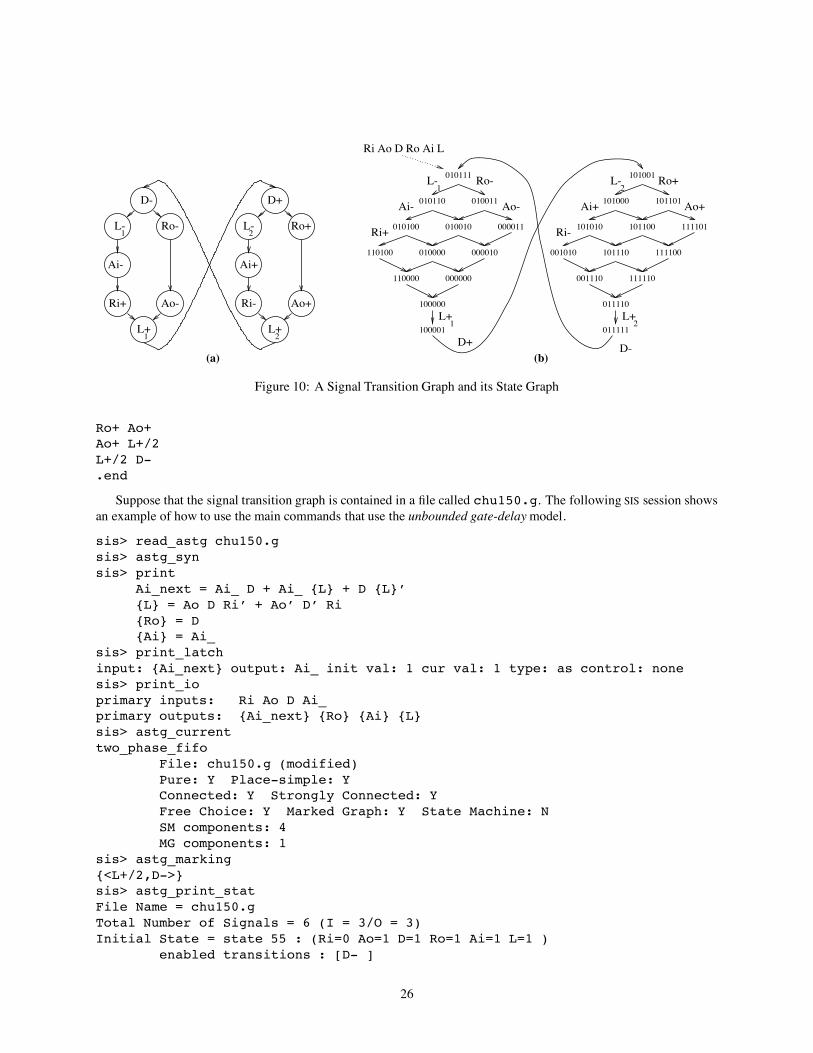
(b)(a)
2
2
D-
L+
Ri-
Ai+
L-
Ao+
Ro+
011111
011110
001110
001010
111110
101110
101010
111100
101100
101000
111101
101101
101001010111
010011
000011
010110
010010010100
110100 010000 000010
000000110000
100000
100001
Ro-
Ao-
L-
Ai-
Ri+
L+
D+
1
1
Ri Ao D Ro Ai L
D-
Ai-
Ri+
L+
Ao-
Ro-
D+
L-
Ai+
Ri- Ao+
Ro+
L+
L-1
1
2
2
Figure 10: A Signal Transition Graph and its State Graph
Ro+ Ao+Ao+ L+/2L+/2 D-.end
Suppose that the signal transition graph is contained in a file called chu150.g. The following SIS session showsan example of how to use the main commands that use the unbounded gate-delaymodel.
sis> read_astg chu150.gsis> astg_synsis> print
Ai_next = Ai_ D + Ai_ {L} + D {L}’{L} = Ao D Ri’ + Ao’ D’ Ri{Ro} = D{Ai} = Ai_
sis> print_latchinput: {Ai_next} output: Ai_ init val: 1 cur val: 1 type: as control: nonesis> print_ioprimary inputs: Ri Ao D Ai_primary outputs: {Ai_next} {Ro} {Ai} {L}sis> astg_currenttwo_phase_fifo
File: chu150.g (modified)Pure: Y Place-simple: YConnected: Y Strongly Connected: YFree Choice: Y Marked Graph: Y State Machine: NSM components: 4MG components: 1
sis> astg_marking{<L+/2,D->}sis> astg_print_statFile Name = chu150.gTotal Number of Signals = 6 (I = 3/O = 3)Initial State = state 55 : (Ri=0 Ao=1 D=1 Ro=1 Ai=1 L=1 )
enabled transitions : [D- ]
26

Total Number of States = 26sis>
astg syn automatically computes an initial marking, printed with astg marking, that corresponds to the (implicit)place between 2 and being marked, and hence to the state labeled 011111 in the state graph.
Note that the function of signal Ai depends on the signal itself. In order to break the asynchronous feedback loop,an asynchronous latch is inserted between primary output Ai next and primary input Ai . So each output signal that ispart of an asynchronous feedback loop is represented inside SIS by three distinct signals:
a “fictitious” primary input (distinguished by “ ”),
a “fictitious” primary output (distinguished by “ next”),
a “real” primary output.
All three signals, though, are actually directly connected to each other, since an asynchronous latch represents only adelay element used to break the loop. This representation trick is required to describe an asynchronous circuit withina framework better suited for synchronous systems.
Signals L and Ro, on the other hand, are purely combinational, hence they are just represented as a combinationallogic block.
Now we can examine a similar session using the bounded wire-delaymodel commands.
sis> read_astg chu150.gsis> astg_to_fsis> print
{Ro_next} = D[15] = Ai_ D + Ai_ L_ + D L_’{Ai} = Ai_[17] = Ao D Ri’ + Ao’ D’ Ri{L} = L_
sis> print_latchinput: {[15]} output: Ai_ init val: 1 cur val: 3 type: as control: noneinput: {[17]} output: L_ init val: 1 cur val: 3 type: as control: nonesis> print_ioprimary inputs: Ri Ao D Ai_ L_primary outputs: {Ro_next} {Ai} {L} {[15]} {[17]}sis> read_library asynch.genlibsis> map -Wsis> print_latchinput: {[587]} output: Ai_ init val: 1 cur val: 3 type: as control: noneinput: {[586]} output: L_ init val: 1 cur val: 3 type: as control: nonesis> print_ioprimary inputs: Ri Ao D Ai_ L_primary outputs: {Ro_next} {Ai} {L} {[587]} {[586]}sis> print_gate -sao33:combinational : 1 (area=64.00)delay:asynch : 1 (area=0.00)inv:combinational : 3 (area=16.00)nor2:combinational : 2 (area=24.00)sr_nor:asynch : 1 (area=40.00)Total: 8 gates, 200.00 areasis> print_delay -ap 1 o()... using library delay model
27
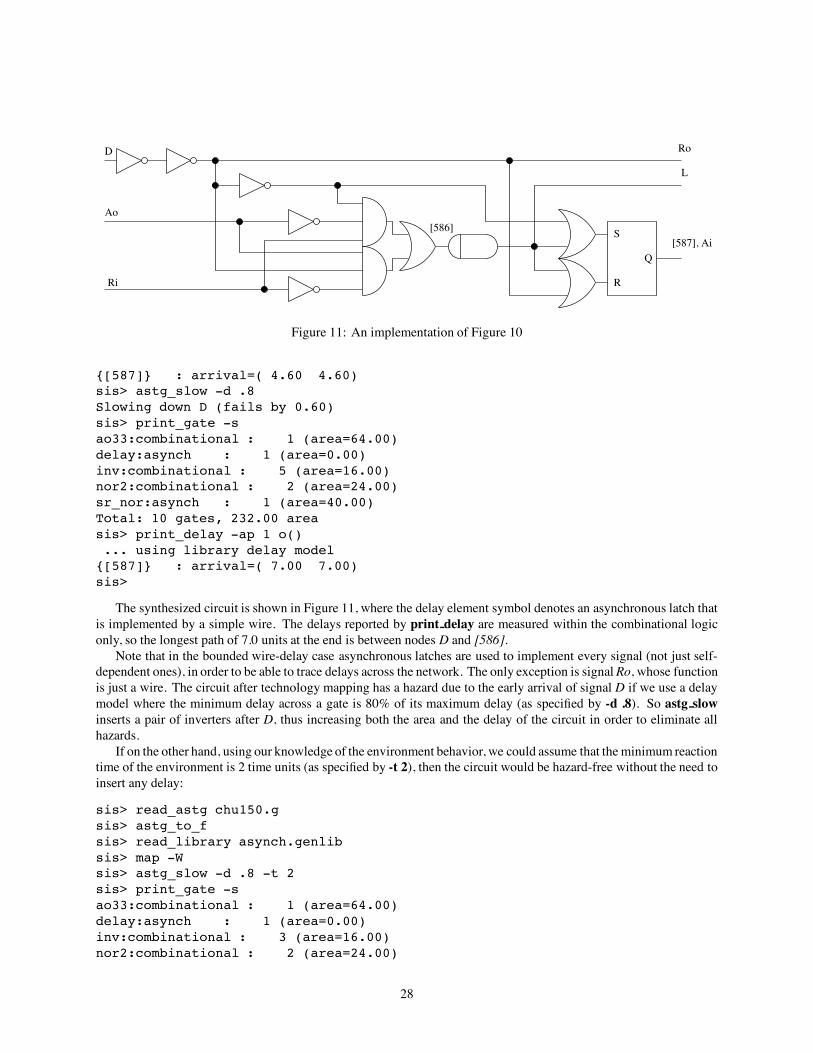
S
R
Q[587], Ai
[586]
Ri
Ao
D Ro
L
Figure 11: An implementation of Figure 10
{[587]} : arrival=( 4.60 4.60)sis> astg_slow -d .8Slowing down D (fails by 0.60)sis> print_gate -sao33:combinational : 1 (area=64.00)delay:asynch : 1 (area=0.00)inv:combinational : 5 (area=16.00)nor2:combinational : 2 (area=24.00)sr_nor:asynch : 1 (area=40.00)Total: 10 gates, 232.00 areasis> print_delay -ap 1 o()... using library delay model
{[587]} : arrival=( 7.00 7.00)sis>
The synthesized circuit is shown in Figure 11, where the delay element symbol denotes an asynchronous latch thatis implemented by a simple wire. The delays reported by print delay are measured within the combinational logiconly, so the longest path of 7.0 units at the end is between nodes D and [586].
Note that in the bounded wire-delay case asynchronous latches are used to implement every signal (not just self-dependent ones), in order to be able to trace delays across the network. The only exception is signalRo, whose functionis just a wire. The circuit after technology mapping has a hazard due to the early arrival of signal D if we use a delaymodel where the minimum delay across a gate is 80% of its maximum delay (as specified by -d .8). So astg slowinserts a pair of inverters after D, thus increasing both the area and the delay of the circuit in order to eliminate allhazards.
If on the other hand, using our knowledge of the environment behavior, we could assume that the minimum reactiontime of the environment is 2 time units (as specified by -t 2), then the circuit would be hazard-free without the need toinsert any delay:
sis> read_astg chu150.gsis> astg_to_fsis> read_library asynch.genlibsis> map -Wsis> astg_slow -d .8 -t 2sis> print_gate -sao33:combinational : 1 (area=64.00)delay:asynch : 1 (area=0.00)inv:combinational : 3 (area=16.00)nor2:combinational : 2 (area=24.00)
28

sr_nor:asynch : 1 (area=40.00)Total: 10 gates, 200.00 areasis> print_delay -ap 1 o()... using library delay model
{[587]} : arrival=( 4.60 4.60)sis>
5 ConclusionsSIS is a comprehensive system for synthesizing and optimizing sequential circuits. It is easily interfaced with otherdesign tools through widely used interchange formats, and integrates a number of state-of-the-art algorithms forsynthesis, optimization, testing, and verification. Several scripts are provided to automate the synthesis process and toserve as a starting point for experimentation with the parameters of each algorithm. SIS targets specifically a sequentialcircuit design methodology and thereby can exploit properties specific to sequential circuits.
6 AcknowledgementsSIS is a joint project supported by theprofessors (in particular ProfessorsBrayton,Newton, andSangiovanni-Vincentelli)and many of the graduate students in the CAD group at U.C. Berkeley. Many of the ideas about sequential andcombinational logic synthesis have originated in the advanced classes and research seminars within the group. Manystudents have contributed code and participated in the development of SIS : Luciano Lavagno, Sharad Malik, ChoMoon, RajeevMurgai, Alex Saldanha, Hamid Savoj, Ellen Sentovich,Narendra Shenoy, Tom Shiple,Kanwar Jit Singh,Moshe Steiner, Paul Stephan, Colin Stevens, Herve Touati and Huey-YihWang. Several programs are distributedwithSIS : JEDI (state assignment) contributed by Bill Lin, NOVA (state assignment) contributedby TizianoVilla, and STAMINA(state minimization) contributed by June-Kyung Rho at the University of Colorado at Boulder. Tony Ma wrote theSENUM program upon which the STG extraction algorithm is based. We gratefully acknowledge the support of NSFunder grant EMC-8419744, DARPA under grant JFBI90-073, the SRC, the state of CaliforniaMICRO program, Intel,AT&T, DEC, and Motorola.
References[1] VAX DECSIM Reference Manual. Digital Equipment Corporation, December 1985. Not generally available.
[2] Karen A. Bartlett, Robert K. Brayton, Gary D. Hachtel, Reily M. Jacoby, Christopher R. Morrison, Richard L.Rudell, Alberto Sangiovanni-Vincentelli, and Albert R. Wang. Multilevel Logic Minimization Using ImplicitDon’t Cares. IEEE Transactions on Computer-Aided Design, 7(6):723–740, June 1988.
[3] R.K. Brayton and C. McMullen. The Decomposition and Factorization of Boolean Expressions. In Proceedingsof the International Symposium on Circuits and Systems, pages 49–54, May 1982.
[4] Robert K. Brayton, Gary D. Hachtel, Curtis T. McMullen, and Alberto L. Sangiovanni-Vincentelli. LogicMinimization Algorithms for VLSI Synthesis. Kluwer Academic Publishers, 1984.
[5] Robert K.Brayton,Richard Rudell,Alberto Sangiovanni-Vincentelli, andAlbert R.Wang.MIS: AMultiple-LevelLogic Optimization System. IEEE Transactions on Computer-Aided Design, CAD-6(6):1062–1081, November1987.
[6] R. Bryant. Graph-based Algorithms for Boolean Function Manipulation. IEEE Transactions on Computers,C-35, August 1986.
[7] J. A. Brzozowski and C-J. Seger. Advances in Asynchronous Circuit Theory – Part I: Gate and UnboundedInertial Delay Models. Bulletin of the European Association of Theoretical Computer Science, October 1990.
29

[8] T. A. Chu. Synthesis of Self-timed VLSI Circuits from Graph-theoretic Specifications. PhD thesis, MIT, June1987.
[9] T. A. Chu. Synthesis of Hazard-free Control Circuits from Asynchronous Finite State Machine Specifications.In ACM Intl. Workshop on Timing Issues in the Specification and Synthesis of Digital Systems, pages 1–10, 1992.
[10] O. Coudert, C. Berthet, and J.C. Madre. Verification of Sequential Machines Based on Symbolic Execution. InProc. of the Workshop on Automatic Verification Methods for Finite State Systems, Grenoble, France, 1989.
[11] G. DeMicheli. Synchronous Logic Synthesis: Algorithms for Cycle-Time Minimization. IEEE Transactions onComputer-Aided Design, 10(1):63–73, January 1991.
[12] Andrea Casotto editor. Octtools-5.1Manuals. In UCB Electronics Research Lab, September 1991.
[13] A. Gamal et. al. An Architecture for Electrically ConfigurableGate Arrays. IEEE Journal of Solid-StateCircuits,24(2):394–398,April 1989.
[14] R.J. Francis, J. Rose, and Z. Vranesic. Chortle-crf: Fast Technology Mapping for Lookup Table-Based FPGAs.In Proceedings of the Design Automation Conference, pages 227–233, June 1991.
[15] G. De Micheli. Synchronous logic synthesis. In International Workshop on Logic Synthesis, page 5.2, NorthCarolina, May 1989.
[16] Abhijit Ghosh. Techniques for Test Generation and Verification in VLSI Sequential Circuits. UCB PhD The-sis, Electronics Research Laboratory, College of Engineering, University of California, Berkeley, CA 94720,December 1991.
[17] G.D. Hachtel, J.-K. Rho, F. Somenzi, and R. Jacoby. Exact and Heuristic Algorithms for the Minimization ofIncompletely Specified State Machines. In The Proceedings of the European Conference on Design Automation,pages 184–191, Amsterdam, The Netherlands, February 1991.
[18] Xilinx Inc. Xilinx Programmable Gate Array User’s Guide, 1988.
[19] T. Larrabee. Efficient Generation of Test Patterns Using Boolean Difference. In Proceedings of the InternationalTest Conference, pages 795–801, 1989.
[20] L. Lavagno, K. Keutzer, and A. Sangiovanni-Vincentelli. Algorithms for Synthesis of Hazard-free AsynchronousCircuits. In Proceedings of the Design Automation Conference, pages 302–308, June 1991.
[21] C. E. Leiserson, F. M. Rose, and J. B. Saxe. Optimizing Synchronous Circuitry by Retiming. In AdvancedResearch in VLSI: Proceedings of the Third Caltech Conference, pages 86–116. Computer Science Press, 1983.
[22] C. E. Leiserson and J. B. Saxe. Retiming Synchronous Circuitry. In TM 372, MIT/LCS, 545 Technology Square,Cambridge, Massachusetts 02139, October 1988.
[23] C.E. Leiserson and J.B. Saxe. Optimizing Synchronous Systems. Journal of VLSI and Computer Systems,1(1):41–67, Spring 1983.
[24] B. Lin and A.R. Newton. Synthesis of Multiple Level Logic from Symbolic High-Level Description Languages.In Proceedings of the International Conference on VLSI, pages 187–196, August 1989.
[25] B. Lin, H. Touati, and A.R. Newton. Don’t Care Minimization of Multi-level Sequential Logic Networks. InProceedings of the International Conference on Computer-Aided Design, pages 414–417, November 1990.
[26] R. Lisanke. Logic synthesis benchmark circuits for the International Workshop on Logic Synthesis, May, 1989.
30
[27] A. Malik, R.K. Brayton, and A.L. Sangiovanni-Vincentelli. AModified Approach to Two-level Logic Minimiza-tion. In Proceedings of the International Conference on Computer-Aided Design, pages 106–109, November1988.
[28] S.Malik, E.M. Sentovich, R.K.Brayton, andA. Sangiovanni-Vincentelli.Retiming and resynthesis: Optimizationof sequential networkswith combinational techniques. IEEE Transactionson Computer-AidedDesign, 10(1):74–84, January 1991.
[29] S. Malik, K.J. Singh, R.K. Brayton, and A. Sangiovanni-Vincentelli. Performance Optimization of PipelinedCircuits. In Proceedings of the International Conference on Computer-Aided Design, pages 410–413, November1990.
[30] H.-J. Mathony. Universal Logic Design Algorithm and its Application to the Synthesis of Two-level SwitchingCircuits. IEE Proceedings, 136 Pt. E(3), May 1989.
[31] M.C. Paull and S.H. Unger. Minimizing the Number of States in Incompletely Specified Sequential SwitchingFunctions. IRE Transactions on Electronic Computers, EC-8:356–367, September 1959.
[32] C. W. Moon, P. R. Stephan, and R. K. Brayton. Synthesis of Hazard-free Asynchronous Circuits from GraphicalSpecifications. In Proceedings of the International Conference on Computer-Aided Design, pages 322–325,November 1991.
[33] C.W. Moon, B. Lin, H. Savoj, and R.K. Brayton. Technology Mapping for Sequential Logic Synthesis. In Proc.Int’l. Workshop on Logic Synthesis, North Carolina, May 1989.
[34] R. Murgai, Y. Nishizaki, N. Shenoy, R. K. Brayton, and A. Sangiovanni Vincentelli. Logic Synthesis forProgrammable Gate Arrays. In Proceedings of the Design Automation Conference, pages 620–625, June 1990.
[35] R. Murgai, N. Shenoy, R. K. Brayton, and A. Sangiovanni Vincentelli. Improved Logic Synthesis Algorithmsfor Table Look Up Architectures. In Proceedings of the International Conference on Computer-Aided Design,pages 564–567, November 1991.
[36] R. Murgai, N. Shenoy, R. K. Brayton, and A. Sangiovanni Vincentelli. Performance Directed Synthesis forTable Look Up Programmable Gate Arrays. In Proceedings of the International Conference on Computer-AidedDesign, pages 572–575, November 1991.
[37] C. Pixley and G. Beihl. Calculating Resetability and Reset Sequences. In Proceedings of the InternationalConference on Computer-Aided Design, November 1991.
[38] J.P. Roth and R.M. Karp. Minimization over Boolean Graphs. In IBM Journal of Research and Development,April 1982.
[39] R. Rudell. Logic Synthesis for VLSI Design. Memorandum No. UCB/ERL M89/49, Electronics ResearchLaboratory, College of Engineering, University of California, Berkeley, CA 94720, April 1989.
[40] Alexander Saldanha, Albert Wang, Robert K. Brayton, and Alberto L. Sangiovanni-Vincentelli. Multi-LevelLogic Simplification using Don’t Cares and Filters. In Proceedings of the Design Automation Conference, pages277–282, 1989.
[41] H. Savoj and R.K. Brayton. The Use of Observability and External Don’t Cares for the Simplification ofMulti-Level Networks. In Proceedings of the Design Automation Conference, pages 297–301, June 1990.
[42] H. Savoj, R.K. Brayton, and H. Touati. Extracting Local Don’t Cares for Network Optimization. In Proceedingsof the International Conference on Computer-Aided Design, November 1991.
[43] H. Savoj, H.-Y. Wang, and R.K. Brayton. Improved Scripts in MIS-II for Logic Minimizaton of CombinationalCircuits. In The International Workshop on Logic Synthesis, May 1991.
31
[44] JamesB. Saxe. Decomposable Searching Problems andCircuit Optimization byRetiming: Two Studies in GeneralTransformations of Computational Structures. CMU-CS-85-162, Carnegie-Mellon University, Department ofComputer Science, August 1985.
[45] R. Segal. BDSYN: Logic Description Translator; BDSIM: Switch-Level Simulator. Master’s Thesis, Memoran-dum No. UCB/ERLM87/33, Electronics Research Laboratory, College of Engineering, University of California,Berkeley, CA 94720, May 1987.
[46] E.M. Sentovich and R.K. Brayton. Preserving Don’t Care Conditions During Retiming. In Proceedings of theInternational Conference on VLSI, pages 461–470, August 1991.
[47] K.J. Singh and A. Sangiovanni-Vincentelli. A Heuristic Algorithm for the Fanout Problem. In Proceedings ofthe Design Automation Conference, pages 357–360, June 1990.
[48] K.J. Singh, A.R. Wang, R.K. Brayton, and A. Sangiovanni-Vincentelli. Timing Optimization of CombinationalLogic. In Proceedings of the International Conference on Computer-Aided Design, pages 282–285, November1988.
[49] A. Srinivasan, T. Kam, S. Malik, and R.K. Brayton. Algorithms for Discrete Function Manipulation. InProceedings of the International Conference on Computer-Aided Design, pages 92–95, November 1990.
[50] H. Touati and R.K. Brayton. Computing the Initial States of Retimed Circuits. IEEE Transactions on Computer-Aided Design, July 1992. To appear.
[51] H. Touati, C. Moon, R.K. Brayton, and A.Wang. Performance-Oriented Technology Mapping. In Proceedingsof the sixth MIT VLSI Conference, pages 79–97, April 1990.
[52] H. Touati, H. Savoj, and R.K. Brayton. Delay Optimization of Combinational Logic Circuits by Clustering andPartial Collapsing. In Proceedings of the International Conference on Computer-Aided Design, November 1991.
[53] H. Touati, H. Savoj, B. Lin, R.K. Brayton, and A.L. Sangiovanni-Vincentelli. Implicit State Enumeration ofFinite State Machines using BDD’s. In Proceedings of the International Conference on Computer-Aided Design,pages 130–133, November 1990.
[54] Herve J.Touati. Performance-OrientedTechnologyMapping.MemorandumNo.UCB/ERLM90/109,ElectronicsResearch Laboratory, College of Engineering, University of California, Berkeley, CA 94720, November 1990.
[55] S. H. Unger. Asynchronous Sequential Switching Circuits. Wiley Interscience, 1969.
[56] P. Vanbekbergen, G. Goossens, and H. De Man. A Local Optimization Technique for Asynchronous ControlCircuits. In Proc. Int’l. Workshop on Logic Synthesis, North Carolina, May 1991.
[57] J. Vasudevamurthy and J. Rajski. A Method for Concurrent Decomposition and Factorization of BooleanExpressions. In Proceedings of the International Conference on Computer-Aided Design, pages 510–513,November 1990.
[58] T. Villa and A. Sangiovanni-Vincentelli. NOVA: State Assignment of Finite State Machines for Optimal Two-Level Logic Implementations. IEEE Transactions on Computer-Aided Design, 9(9):905–924, September 1990.
32

Appendix A : Berkeley Logic Interchange Format (BLIF)The goal of BLIF is to describe a logic-level hierarchical circuit in textual form. A circuit is an arbitrary combinationalor sequential network of logic functions. A circuit can be viewed as a directed graph of combinational logic nodes andsequential logic elements. Each node has a two-level, single-output logic function associated with it. Each feedbackloop must contain at least one latch. Each net (or signal) has only a single driver, and either the signal or the gatewhich drives the signal can be named without ambiguity.
In the following, angle-brackets surround nonterminals, and square-brackets surround optional constructs.
1 ModelsA model is a flattened hierarchical circuit. A BLIF file can contain many models and references to models described inother BLIF files. A model is declared as follows:
.model <decl-model-name>
.inputs <decl-input-list>
.outputs <decl-output-list>
.clock <decl-clock-list><command>
.
.
.<command>.end
decl-model-name is a string giving the name of the model.
decl-input-list is a white-space-separated list of strings (terminated by the end of the line) giving the formal inputterminals for the model being declared. If this is the first or only model, then these signals can be identified asthe primary inputs of the circuit. Multiple .inputs lines are allowed, and the lists of inputs are concatenated.
decl-output-list is a white-space-separated list of strings (terminated by the end of the line) giving the formal outputterminals for the model being declared. If this is the first or only model, then these signals can be identified asthe primary outputs of the circuit. Multiple .outputs lines are allowed, and the lists of outputs are concatenated.
decl-clock-list is a white-space-separated list of strings (terminated by the end of the line) giving the clocks for themodel being declared. Multiple .clock lines are allowed, and the lists of clocks are concatenated.
command is one of:<logic-gate> <generic-latch> <library-gate><model-reference> <subfile-reference> <fsm-description><clock-constraint> <delay-constraint>
Each command is described in the following sections.
The BLIF parser allows the .model, .inputs, .outputs, .clock and .end statements to be optional. If .model is notspecified, the decl-model-name is assigned the name of the BLIF file being read. It is an error to use the same string fordecl-model-name in more than one model. If .inputs is not specified, it can be inferred from the signals which are notthe outputs of any other logic block. Similarly, .outputs can be inferred from the signals which are not the inputs toany other blocks. If any .inputs or .outputs are given, no inference is made; a node that is not an output and does notfanout produces a warning message.
If .clock is not specified (e.g., for purely combinational circuits) there are no clocks. .end is implied at end of fileor upon encountering another .model.Important: the first model encountered in the main BLIF file is the one returned to the user. The only .clock,
clock-constraint, and timing-constraint constructs retained are the ones in the first model. All subsequent models canbe incorporated into the first model using the model-reference construct.
Anywhere in the file a ‘#’ (hash) begins a comment that extends to the end of the current line. Note that thecharacter ‘#’ cannot be used in any signal names. A ‘\’ (backslash) as the last character of a non-comment lineindicates concatenation of the subsequent line to the current line. No whitespace should follow the ‘\’.
Example:
33

.model simple
.inputs a b
.outputs c
.names a b c # .names described later11 1.end
# unnamed model.names a b \c # ‘\’ here only to demonstrate its use11 1
Both models “simple” and the unnamed model describe the same circuit.
2 Logic GatesA logic-gate associates a logic function with a signal in the model, which can be used as an input to other logicfunctions. A logic-gate is declared as follows:
.names <in-1> <in-2> ... <in-n> <output><single-output-cover>
output is a string giving the name of the gate being defined.
in-1, in-2, ... in-n are strings giving the names of the inputs to the logic gate being defined.
single-output-cover is, formally, an n-input, 1-output PLA description of the logic function corresponding to the logicgate. 0, 1, – is used in the n-bit wide “input plane” and 0, 1 is used in the 1-bit wide “output plane”. TheON-set is specified with 1’s in the “output plane,” and the OFF-set is specified with 0’s in the “output plane.” TheDC-set is specified for primary output nodes only, by using the construct .exdc.
A sample logic-gatewith its single-output-cover:.names v3 v6 j u78 v13.151--0 1-1-1 10-11 1
In a given row of the single-output-cover, “1” means the input is used in uncomplemented form, “0” means theinput is complemented, and “–” means not used. Elements of a row are ANDed together, and then all rows are ORed.
As a result, if the last column (the “output plane”) of the single-output-cover is all 1’s, the first n columns (the“input plane”) of the single-output-cover can be viewed as the truth table for the logic gate named by the string output.The order of the inputs in the single-output-cover is the same as the order of the strings in-1, in-2, ..., in-n in the .namesline. A space between the columns of the “input plane” and the “output plane” is required.
The translation of the above sample logic-gate into a sum-of-products notation would be as follows:v13.15 = (v3 u78’) + (v6 u78) + (v3’ j u78)
To assign the constant “0” to some logic gate j, use the following construct:
.names j
To assign the constant “1”, use the following:.names j1
The string output can be used as the input to another logic-gate before the logic-gate for output is itself defined.For a more complete description of the PLA input format, see espresso(5).
34

3 External Don’t CaresExternal don’t cares are specified as a separate network within a model, and are specified at the end of the modelspecification. Each external don’t care function, which is specified by a .names construct, must be associated with aprimary output of the main model and specified as a function of the primary inputs of the main model (hierarchicalspecification of external don’t cares is currently not supported).
The external don’t cares are specified as follows:.exdc.names <in-1> <in-2> ... <in-n> <output><single-output-cover>
_exdc indicates that the following .names constructs apply to the external don’t care network.
output is a string giving the name of the primary output for which the conditions are don’t cares.
in-1, in-2, ... in-n are strings giving the names of the primary inputs which the don’t care conditions are expressed interms of.
single-output-cover is an n-input, 1-output PLA description of the logic function corresponding to the don’t careconditions for the output.
The following is an example circuit with external don’t cares:.model a.inputs x y.outputs j.subckt b x=x y=y j=j.exdc.names x j1 1.end
.model b
.inputs x y
.outputs j
.names x y j11 1.end
The translation of the above example into a sum-of-products notation would be as follows:j = x * y;external d.c. for j = x;
4 Flip flops and latchesA generic-latch is used to create a delay element in a model. It represents one bit of memory or state information.The generic-latch construct can be used to create any type of latch or flip-flop (see also the library-gate section). Ageneric-latch is declared as follows:
.latch <input> <output> [<type> <control>] [<init-val>]
input is the data input to the latch.
output is the output of the latch.
type is one of fe, re, ah, al, as , which correspond to “falling edge,” “rising edge,” “active high,” “active low,” or“asynchronous.”
control is the clocking signal for the latch. It can be a .clock of the model, the output of any function in the model, orthe word “NIL” for no clock.
35

init-val is the initial state of the latch, which can be one of 0, 1, 2, 3 . “2” stands for “don’t care” and “3” is“unknown.” Unspecified, it is assumed “3.”
If a latch does not have a controlling clock specified, it is assumed that it is actually controlled by a single globalclock. The behavior of this global clock may be interpreted differently by the various algorithms that may manipulatethe model after the model has been read in. Therefore, the user should be aware of these varying interpretations iflatches are specified with no controlling clocks.Important: All feedback loops in a model must go through a generic-latch. Purely combinational-logic cycles
are not allowed.Examples:
.inputs d # a clocked flip-flop
.output q
.clock c
.latch d q re c 0
.end
.inputs in # a very simple sequential circuit
.outputs out
.latch out in 0
.names in out0 1.end
5 Library GatesA library-gate creates an instance of a technology-dependent logic gate and associates it with a node that representsthe output of the logic gate. The logic function of the gate and its known technology dependent delays, drives, etc. arestored with the library-gate. A library-gate is one of the following:
.gate <name> <formal-actual-list>
.mlatch <name> <formal-actual-list> <control> [<init-val>]
name is the name of the .gate or .mlatch to instantiate. A gate or latch with this name must be present in the currentworking library.
formal-actual-list is a mapping between the formal parameters of name (the terminals of the library-gate) and theactual parameters of the current model (any signals in this model). The format for a formal-actual-list is awhite-space-separated sequence of assignment statements of the form:
formal1=actual1 formal2=actual2 ...
All of the formal parameters of name must be specified in the formal-actual-list and the single output of namemust be the last one in the list.
control is the clocking signal for the mlatch, which can be either a .clock of the model, the output of any function inthe model, or the word “NIL” for no clock.
init-val is the initial state of the mlatch, which can be one of 0, 1, 2, 3 . “2” stands for “don’t care” and “3” is“unknown.” Unspecified, it is assumed “3.”
A .gate refers to a two-level representation of an arbitrary input, single output gate in a library. A .gate appearsunder a technology-independent interpretation as if it were a single logic-gate.
A .mlatch refers to a latch (not necessarily a D flip flop) in a library. A .mlatch appears under a technology-independent interpretation as if it were a single generic-latch and possibly a single logic-gate feeding the data input ofthat generic-latch.
36
.gates and .mlatches are used to describe circuits that have been implemented using a specific library of standardlogic functions and their technology-dependent properties. The library of library-gates must be read in before a BLIFfile containing .gate or .mlatch constructs is read in.
The string name refers to a particular gate or latch in the library. The names “nand2,” “inv,” and “jk rising edge”in the following examples are descriptive names for gates in the library. The following BLIF description:
.inputs v1 v2
.outputs j
.gate nand2 A=v1 B=v2 O=x # given: formals of this gate are A, B, O
.gate inv A=x O=j # given: formals of this gate are A & O
.end
could also be specified in a technology-independent way (assuming “nand2” is a 2-input NAND gate and “inv” is anINVERTER) as follows:
.inputs v1 v2
.outputs j
.names v1 v2 x0- 1-0 1.names x j0 1.end
Similarly:.inputs j kbar.outputs out.clock clk.mlatch jk_rising_edge J=j K=k Q=q clk 1 # given: formals are J, K, Q.names q out0 1.names kbar k0 1.end
could have been specified in a technology-independent way (assuming “jk rising edge” is a JK rising-edge-triggeredflip flop) as follows:
.inputs j kbar
.outputs out
.clock clk
.latch temp q re clk 1 # the .latch
.names j k q temp # the .names feeding the D input of the .latch-01 11-0 1.names q out0 1.names kbar k0 1.end
6 Model (subcircuit) referencesA model-reference is used to insert the logic functions of one model into the body of another. It is defined as follows:
.subckt <model-name> <formal-actual-list>
model-name is a string giving the name of the model being inserted. It need not be previously defined in this file, butshould be defined somewhere in either this file, a .search file, or a master file that is .searching this file. (see.search below)
formal-actual-list is a mapping between the formal terminals (the decl-input-list, decl-output-list, and decl-clock-list)of the called model model-name and the actual parameters of the current model. The actual parameters may beany signals in the current model. The format for a formal-actual-list is the same as its format in a library-gate.
37

A .subckt construct can be viewed as creating a copy of the logic functions of the called model model-name,including all of model-name’s generic-latches, in the calling model. The hierarchical nature of the BLIF description ofthe model does not have to be preserved. Subcircuits can be nested, but cannot be self-referential or create a cyclicdependency.
Unlike a library-gate, a model-reference is not limited to one output.The formals need not be specified in the same order as they are defined in the decl-input-list, decl-output-list, or
decl-clock-list; elements of the lists can be intermingled in any order, provided the names are given correctly. Warningmessages are printed if elements of the decl-input-list or decl-clock-list are not driven by an actual parameter or ifelements of the decl-output-list do not fan out to an actual parameter. Elements of the decl-clock-list and decl-input-listmay be driven by any logic function of the calling model.
Example: rather than rewriting the entire BLIF description for a commonly used subcircuit several times, thesubcircuit can be described once and called as many times as necessary:
.model 4bitadder
.inputs A3 A2 A1 A0 B3 B2 B1 B0 CIN
.outputs COUT S3 S2 S1 S0
.subckt fulladder a=A0 b=B0 cin=CIN s=S0 cout=CARRY1
.subckt fulladder a=A3 b=B3 cin=CARRY3 s=S3 cout=COUT
.subckt fulladder b=B1 a=A1 cin=CARRY1 s=XX cout=CARRY2
.subckt fulladder a=JJ b=B2 cin=CARRY2 s=S2 cout=CARRY3# for the sake of example,
.names XX S1 # formal output ‘s’ does not fanout to a primary output1 1.names A2 JJ # formal input ‘a’ does not fanin from a primary input1 1.end
.model fulladder
.inputs a b cin
.outputs s cout
.names a b k10 101 1.names k cin s10 101 1.names a b cin cout11- 11-1 1-11 1.end
7 Subfile ReferencesA subfile-reference is:
.search <file-name>
file-name gives the name of the file to search.
A subfile-reference directs the BLIF reader to read in and define all the models in file file-name. A subfile-referencedoes not have to be inside of a .model. subfile-references can be nested.
Search files would usually be used to hold all the subcircuits referred to in model-references, while the master filemerely searches all the subfiles and instantiates all the subcircuits it needs.
A subfile-reference is not equivalent to including the body of subfile file-name in the current file. It does notpatch fragments of BLIF into the current file; it pauses reading the current file, reads file-name as an independent,self-contained file, then returns to reading the current file.
The first .model in the master file is always the one returned to the user, regardless of any subfile-references thanmay precede it.
38

8 Finite State Machine DescriptionsA sequential circuit can be specified in BLIF logic form, as a finite state machine, or both. An fsm-description is usedto insert a finite state machine description of the current model. It is intended to represent the same sequential circuitas the current model (which contains logic), but in FSM form. The format of an fsm-description is:
.start_kiss
.i <num-inputs>
.o <num-outputs>[.p <num-terms>][.s <num-states>][.r <reset-state>]<input> <current-state> <next-state> <output>
.
.
.<input> <current-state> <next-state> <output>.end_kiss[.latch_order <latch-order-list>][<code-mapping>]
num-inputs is the number of inputs to the FSM, which should agree with the number of inputs in the .inputs constructfor the current model.
num-outputs is the number of outputs of the FSM, which should agree with the number of outputs in the .outputsconstruct for the current model.
num-terms is the number of “<input> <current-state> <next-state> <output>” 4-tuples that follow in the FSMdescription.
num-states is the number of distinct states that appear in “<current-state>” and “<next-state>” columns.
reset-state is the symbolic name for the reset state for the FSM; it should appear somewhere in the “<current-state>”column.
input is a sequence of num-inputsmembers of 0, 1, – .
output is a sequence of num-outputsmembers of 0, 1, – .
current-state and next-state are symbolic names for the current state and next state transitions of the FSM.
latch-order-list is a white-space-separated sequence of latch outputs.
code-mapping is newline separated sequence of:
.code <symbolic-name> <encoded-name>
num-terms and num-states do not have to be specified. If the reset-state is not given, it is assigned to be the firststate encountered in the “<current-state>” column.
The ordering of the bits in the input and output fields will be the same as the ordering of the variables in the .inputsand .outputs constructs if both an fsm-description and logic functions are given.
latch-order-list and code-mapping are meant to be used when both an fsm-description and a logical descriptionof the model are given. The two constructs together provide a correspondence between the latches in the logicaldescription and the state variables in the fsm-description. In a code-mapping, symbolic-name consists of a symbolicname from the “<current-state>” or “<next-state>” columns, and encoded-name is the pattern of bits ( 0, 1 ) thatrepresent the state encoding for symbolic-name. The code-mapping should only be given if both an fsm-descriptionand logic functions are given. .latch-order establishes a mapping between the bits of the encoded-names of thecode-mapping construct and the latches of the network. The order of the bits in the encoded names will be the sameas the order of the latch outputs in the latch-order-list. There should be the same number of bits in the encoded-nameas there are latches if both an fsm-description and a logical description are specified.
39
If both logic-gates and an fsm-description of the model are given, the logic-gate description of the model shouldbe consistent with the fsm-description, that is, they should describe the same circuit. If they are not consistent therewill be no sensible way to interpret the model, which should then cause an error to be returned.
If only the fsm-description of the network is given, it may be run through a state assignment routine and given alogic implementation. A sole fsm-description, having no logic implementation, cannot be inserted into another modelby amodel-reference; the state assigned network, or a network containing both logic-gates and an fsm-description can.
Example of an fsm-description:.model 101 # outputs 1 whenever last 3 inputs were 1, 0, 1.start_kiss.i 1.o 10 st0 st0 01 st0 st1 00 st1 st2 01 st1 st1 00 st2 st0 01 st2 st3 10 st3 st2 01 st3 st1 0.end_kiss.end
Above example with a consistent fsm-description and logical description:.model.inputs v0.outputs v3.2.latch [6] v1 0.latch [7] v2 0.start_kiss.i 1.o 1.p 8.s 4.r st00 st0 st0 01 st0 st1 00 st1 st2 01 st1 st1 00 st2 st0 01 st2 st3 10 st3 st2 01 st3 st1 0.end_kiss.latch_order v1 v2.code st0 00.code st1 11.code st2 01.code st3 10.names v0 [6]1 1.names v0 v1 v2 [7]-1- 11-0 1.names v0 v1 v2 v3.2101 1.end
9 Clock ConstraintsA clock-constraint is used to set up the behavior of the simulated clocks, and to specify how clock events (rising orfalling edges) occur relative to one another. A clock-constraint is one or more of the following:
.cycle <cycle-time>
.clock_event <event-percent> <event-1> [<event-2> ... <event-n>]
40
cycle-time is a floating point number giving the clock cycle time for the model. It is a unitless number that is to beinterpreted by the user.
event-percent is a floating point number representing a percentage of the clock cycle time at which a specific.clock event occurs. Fifty percent is written as “50.0.”
event-1 through event-n are one of the following:
<rise-fall>’<clock-name>(<rise-fall>’<clock-name> <before> <after>)
where rise-fall is either “r” or “f” and stands for the rising or falling edge of the clock and clock-name is a clockfrom the .clock construct. The apostrophe between rise-fall and clock-name is a separator, and serves no purposein and of itself.
before and after are floating point numbers in the same “units” as the cycle-time and are used to define the “skew” inthe clock edges. before represents maximum amount of time before the nominal time that the edge can arrive;after represents the maximum amount of time after the nominal time that the edge can arrive. The nominaltime is event-percent% of the cycle-time. In the unparenthesized form for the clock-event, before and after areassumed “0.0.”
All events, event-1 ... event-n, specified in a single .clock event are to be linked together. A routine changing anyone edge should also modify the occurrence time of all the related clock edges.
Example 1:.clock clock1 clock2.clock_event 50.0 r’clock1 (f’clock2 2.0 5.0)
Example 2:.clock clock1 clock2.clock_event 50.0 r’clock1.clock_event 50.0 (f’clock2 2.0 5.0)
Both examples specify a nominal time of 50% of the cycle time, that the rising edge of clock1 must occur at exactlythe nominal time, and that the falling edge of clock2 may occur from 2.0 units before to 5.0 units after the nominaltime.
In Example 1, if r’clock1 is later moved to a different nominal time by some routine then f’clock2 should also bechanged. However, in Example 2 changing r’clock1 would not affect f’clock2 even though they originally have thesame value of event-percent.
10 Delay ConstraintsA delay-constraint is used to specify parameters to more accurately compute the amount of time signals take topropagate from one point to another in a model. A delay-constraint is one or more of :
.area <area>
.delay <in-name> <phase> <load> <max-load> <brise> <drise> <bfall> <dfall>
.wire_load_slope <load>
.wire <wire-load-list>
.input_arrival <in-name> <rise> <fall> [<before-after> <event>]
.default_input_arrival <rise> <fall>
.output_required <out-name> <rise> <fall> [<before-after> <event>]
.default_output_required <rise> <fall>
.input_drive <in-name> <rise> <fall>
.default_input_drive <rise> <fall>
.output_load <out-name> <load>
.default_output_load <load>
rise, fall, drive, and load are all floating point numbers giving the rise time, fall time, input drive, and output load.
41

in-name is a primary input and out-name is a primary output.
before-after can be one of b, a , corresponding to “before” or “after,” and event has the same format as theunparenthesized form of event-1 in a clock-constraint.
.area sets the area of the model to be area.
.delay sets the delay for input in-name. phase is one of “INV,” “NONINV,” or “UNKNOWN” for inverting, non-inverting,or neither. max-load is a floating point number for the maximum load. brise, drise, bfall, and dfall are floatingpoint numbers giving the block rise, drive rise, block fall, and drive fall for in-name.
.wire load slope sets the wire load slope for the model.
.wire sets the wire loads for the model from the list of floating point numbers in the wire-load-list.
.input arrival sets the input arrival time for the input in-name. If the optional arguments are specified, then the inputarrival time is relative to the event.
.output required sets the output required time for the output out-name. If the optional arguments are specified, thenthe output required time is relative to the event.
.input drive sets the input drive for the input in-name.
.output load sets the output load for the output out-name.
.default input arrival, .default output required, .default input drive, .default output load set the corresponding de-fault values for all the inputs/outputswhose values are not specifically set.
There is no actual unit for all the timing and load numbers. Special attention should be given when specifyingand interpreting the values. The timing numbers are assumed to be in the same “unit” as the cycle-time in the .cycleconstruct.
42

Appendix B : Genlib FormatThis is a description of the genlib format which is used to specify library gates in SIS.
1 Combinational Gate SpecificationA cell is specified in the following format:GATE <cell-name> <cell-area> <cell-logic-function><pin-info>
.
.<pin-info>
<cell-name> is the name of the cell in the cell library. The resulting net-list will be in terms of these names.
<cell-area> defines the relative area cost of the cell. It is a floating point number, and may be in any unit systemconvenient for the user.
<cell-logic-function> is an equation written in conventional algebraic notation using the operators ’+’ for OR, ’*’ ornothing (space) for AND, ’!’ or ”’ (post-fixed) for NOT, and parentheses for grouping. The names of the literalsin the equation define the input pin names for the cell; the name on the left hand side of the equation defines theoutput of the cell. The equation terminates with a semicolon.
Only single-output cells may be specified. The ’!’ operator may only be used on the input literals, or on the finaloutput; it is not allowed internal to an expression. (This constraint may disappear in the future).
Also, the actual factored form is significant when a logic function has multiple factored forms. In principle, allfactored forms could be derived for a given logic function automatically; this is not yet implemented, so each must bespecified separately. Note that factored forms which differ by a permutation of the input variables (or by De Morgan’slaw) are not considered unique.
Each <pin-info> has the format:
PIN <pin-name> <phase> <input-load> <max-load><rise-block-delay> <rise-fanout-delay><fall-block-delay> <fall-fanout-delay>
<pin-name> must be the name of a pin in the <cell-logic-function>, or it can be * to specify identical timinginformation for all pins.
<phase> is INV, NONINV, or UNKNOWN corresponding to whether the logic function is negative-unate, positive-unate, or binate in this input variable respectively. This is required for the separate rise-fall delay model. (Inprinciple, this information is easily derived from the logic function; this field may disappear in the future).
<input-load> gives the input load of this pin. It is a floating point value, in arbitrary units convenient for the user.
<max-load> specifies a loading constraint for the cell. It is a floating point value specifying the maximum loadallowed on the output.
<rise-block-delay> and <rise-fanout-delay> are the rise-time parameters for the timing model. They are floatingpoint values, typically in the units nanoseconds, and nanoseconds/unit-load respectively.
<fall-block-delay> and <fall-fanout-delay> are the fall-time parameters for the timing model. They are floatingpoint values, typically in the units nanoseconds, and nanoseconds/unit-load repsectively.
All of the delay information is specified on a pin-by-pin basis. The meaning is the delay information for the mostcritical pin is used to determine the delay for the gate.
43
2 Latch SpecificationLatches are specified as follows:
LATCH <cell-name> <cell-area> <cell-logic-function><pin-info>
.
.<pin-info><latch-spec>[<clock-delay-info>][<constraint-info>]
<cell-name>, <cell-area>, <cell-logic-function> and <pin-info> are the same as in the combinational case.
<latch-spec> has the following format:
SEQ <latch-input> <latch-output> <latch-type>
<latch-input> must be the name of the output of the cell. Thus, <latch-input> is described as a function of<latch-output> in the <cell-logic-function>. A special name "ANY" can be used for <latch-output> to specifyto the mapper that <latch-output> needs not be a signal name in the <cell-logic-function>. This is useful fordescribingD-type flip-flops and latches. <latch-type> can be ACTIVE HIGH orACTIVE LOW for transparentlatches; RISING EDGE or FALLING EDGE for edge-triggeredflip-flops; or ASYNCH for asychronous latches.
<clock-delay-info> is necessary for synchronous latches and flip-flops. It gives the propagation delay from the clockpin to the output. Its format is as follows:
CONTROL <clock-pin-name> <input-load> <max-load><rise-block-delay> <rise-fanout-delay><fall-block-delay> <fall-fanout-delay>
<constraint-info> gives the setup and hold time constraints with respect to the clock signal. The format is:
CONSTRAINT <pin-name> <setup-time> <hold-time>
If not specified, the values of 0.0 are assumed.
3 ExamplesExample 0 of latch specification:
LATCH "d-latch" 80 Q=D;PIN D NONINV 1 999 1 .2 1 .2SEQ Q ANY ACTIVE_HIGHCONTROL CLK 1 999 1 .2 1 .2CONSTRAINT D 0.2 0.2
Example 1 of <cell-logic-function>:
O = !(!I1 * I2);
This is legal and defines a NAND gate with 1 inverted input; it could also be specified as
O = I1 + !I2;
There is no advantage or disadvantage to either representation; only one need be given.Example 2 of <cell-logic-function>:
44

O = !((I1 * I2) + !(I3 + I4));
is incorrectly specified. It must be re-written as either
O = !((I1 * I2) + (!I3 * !I4));
or
O = (!I1 + !I2)*(I3 + I4);
Again, there is no advantage or disadvantage to either representation as they differ only by DeMorgan’s law. Onlyone need be given. Note that there are no other factored forms for this equation.Example 3 of <cell-logic-function>:
O = a*b + a*c + b*c;
This is one specification of a majority gate. Another possible specification (which IS considered different) is:
O = a*(b + c) + b*c;
Any permutation of the input variables does not provide a new specification; hence, these are the only two usefulrepresentations for a majority gate logic function. Both should be provided to the technology mapping program, untilfurther notice.
45


![Sequential Ordering Algorithm for Mass Integration: The Case ...[24]-[26], simultaneous mass and property integration considering also thermal constraints [27], and the synthe sis](https://img.pdfslide.us/doc/110x75/60e0a1a715dbb542d17684d4/sequential-ordering-algorithm-for-mass-integration-the-case-24-26-simultaneous.jpg)