Embed Size (px)
Citation preview
Single defect centers in diamondnanocrystals as quantum probes for
plasmonic nanostructures
Andreas W. Schell,1* Gunter Kewes,1 Tobias Hanke,2 AlfredLeitenstorfer,2 Rudolf Bratschitsch,2 Oliver Benson1 and Thomas
Aichele1
1Humboldt-Universitat zu Berlin, Institute of Physics,Newtonstraße 15, D-12489 Berlin, Germany
2University of Konstanz, Department of Physics and Center for Applied Photonics,Universittsstraße 10, D-78464 Konstanz, Germany
Abstract: We present two applications of a single nitrogen vacancycenter in a nanodiamond as quantum probe for plasmonic nanostructures.Coupling to the nanostructures is achieved in a highly controlled manner bypicking up a pre-characterized nanocrystal with an atomic force microscopeand placing it at the desired position. Local launching of single excitationsinto a nanowire with a spatial control of few nanometers is demonstrated.Further, a two dimensional map of the electromagnetic environment of aplasmonic bowtie antenna was derived, resembling an ultimate limit offluorescence lifetime nanoscopy.
© 2011 Optical Society of America
OCIS codes: (180.4243) Near-field microscopy; (240.6680) Surface plasmons; (130.3120) In-tegrated optics devices.
References and links1. T. A. Kennedy, J. S. Colton, J. E. Butler, R. C. Linares, and P. J. Doering, “Long coherence times at 300 k for
nitrogen-vacancy center spins in diamond grown by chemical vapor deposition,” Appl. Phys. Lett. 83, 4190–4192(2003).
2. F. Jelezko and J. Wrachtrup, “Single defect centres in diamond: A review,” Phys. Stat. Sol. (a) 203, 3207–3225(2006).
3. R. Brouri, A. Beveratos, J.-P. Poizat, and P. Grangier, “Photon antibunching in the fluorescence of individualcolor centers in diamond,” Opt. Lett. 25, 1294–1296 (2000).
4. C. Kurtsiefer, S. Mayer, P. Zarda, and H. Weinfurter, “Stable solid-state source of single photons,” Phys. Rev.Lett. 85, 290–293 (2000).
5. T. Schroder, A. W. Schell, G. Kewes, T. Aichele, and O. Benson, “Fiber-integrated diamond-based single photonsource,” Nano Lett. 11, 198–202 (2010).
6. J. Wolters, A. W. Schell, G. Kewes, N. Nusse, M. Schoengen, H. Doscher, T. Hannappel, B. Lochel, M. Barth,and O. Benson, “Enhancement of the zero phonon line emission from a single nitrogen vacancy center in ananodiamond via coupling to a photonic crystal cavity,” Appl. Phys. Lett. 97, 141108 (2010).
7. T. D. Ladd, F. Jelezko, R. Laflamme, Y. Nakamura, C. Monroe, and J. L. O’Brien, “Quantum computers,” Nature464, 45–53 (2010).
8. G. Balasubramanian, I. Y. Chan, R. Kolesov, M. Al-Hmoud, J. Tisler, C. Shin, C. Kim, A. Wojcik, P. R. Hem-mer, A. Krueger, T. Hanke, A. Leitenstorfer, R. Bratschitsch, F. Jelezko, and J. Wrachtrup, “Nanoscale imagingmagnetometry with diamond spins under ambient conditions,” Nature 455, 648–651 (2008).
9. J. R. Maze, P. L. Stanwix, J. S. Hodges, S. Hong, J. M. Taylor, P. Cappellaro, L. Jiang, M. V. G. Dutt, E. Togan,A. S. Zibrov, A. Yacoby, R. L. Walsworth, and M. D. Lukin, “Nanoscale magnetic sensing with an individualelectronic spin in diamond,” Nature 455, 645–648 (2008).
#142539 - $15.00 USD Received 10 Feb 2011; revised 25 Feb 2011; accepted 26 Feb 2011; published 8 Apr 2011(C) 2011 OSA 11 April 2011 / Vol. 19, No. 8 / OPTICS EXPRESS 7914
10. Y. Sonnefraud, A. Cuche, O. Faklaris, J.-P. Boudou, T. Sauvage, J.-F. Roch, F. Treussart, and S. Huant, “Diamondnanocrystals hosting single nitrogen-vacancy color centers sorted by photon-correlation near-field microscopy,”Opt. Lett. 33, 611–613 (2008).
11. E. Rittweger, K. Y. Han, S. E. Irvine, C. Eggeling, and S. W. Hell, “Sted microscopy reveals crystal colour centreswith nanometric resolution,” Nat. Phot. 3, 144–147 (2009).
12. A. Cuche, O. Mollet, A. Drezet, and S. Huant, “”Deterministic” quantum plasmonics,” Nano Lett. 10, 4566–4570(2010).
13. W. L. Barnes, A. Dereux, and T. W. Ebbesen, “Surface plasmon subwavelength optics,” Nature 424, 824–830(2003).
14. H. Ditlbacher, A. Hohenau, D. Wagner, U. Kreibig, M. Rogers, F. Hofer, F. R. Aussenegg, and J. R. Krenn,“Silver nanowires as surface plasmon resonators,” Phys. Rev. Lett. 95, 257403 (2005).
15. Z. Li, K. Bao, Y. Fang, Y. Huang, P. Nordlander, and H. Xu, “Correlation between incident and emission polar-ization in nanowire surface plasmon waveguides,” Nano Lett. 10, 1831–1835 (2010).
16. M. W. Knight, N. K. Grady, R. Bardhan, F. Hao, P. Nordlander, and N. J. Halas, “Nanoparticle-mediated couplingof light into a nanowire,” Nano Lett. 7, 2346–2350 (2007).
17. R. Kolesov, B. Grotz, G. Balasubramanian, R. J. Stohr, A. A. L. Nicolet, P. R. Hemmer, F. Jelezko, andJ. Wrachtrup, “Wave-particle duality of single surface plasmon polaritons,” Nat. Phys. 5, 470–474 (2009).
18. A. V. Akimov, A. Mukherjee, C. L. Yu, D. E. Chang, A. S. Zibrov, P. R. Hemmer, H. Park, and M. D. Lukin,“Generation of single optical plasmons in metallic nanowires coupled to quantum dots,” Nature 450, 402–406(2007).
19. Y. Fedutik, V. V. Temnov, O. Schops, U. Woggon, and M. V. Artemyev, “Exciton-plasmon-photon conversion inplasmonic nanostructures,” Phys. Rev. Lett. 99, 136802 (2007).
20. H. Wei, D. Ratchford, X. E. Li, H. Xu, and C.-K. Shih, “Propagating surface plasmon induced photon emissionfrom quantum dots,” Nano Lett. 9, 4168–4171 (2009).
21. M. Barth, N. Nusse, B. Lochel, and O. Benson, “Controlled coupling of a single-diamond nanocrystal to aphotonic crystal cavity,” Opt. Lett. 34, 1108–1110 (2009).
22. S. Schietinger, M. Barth, T. Aichele, and O. Benson, “Plasmon-enhanced single photon emission from ananoassembled metaldiamond hybrid structure at room temperature,” Nano Lett. 9, 1694–1698 (2009).
23. D. E. Chang, A. S. Sørensen, P. R. Hemmer, and M. D. Lukin, “Quantum optics with surface plasmons,” Phys.Rev. Lett. 97, 053002 (2006).
24. P. Muhlschlegel, H.-J. Eisler, O. J. F. Martin, B. Hecht, and D. W. Pohl, “Resonant optical antennas,” Science308, 1607–1609 (2005).
25. O. L. Muskens, V. Giannini, J. A. Sanchez-Gil, and J. Gomez Rivas, “Strong enhancement of the radiative decayrate of emitters by single plasmonic nanoantennas,” Nano Lett. 7, 2871–2875 (2007).
26. R. Esteban, T. V. Teperik, and J. J. Greffet, “Optical patch antennas for single photon emission using surfaceplasmon resonances,” Phys. Rev. Lett. 104, 026802 (2010).
27. A. Kinkhabwala, Z. Yu, S. Fan, Y. Avlasevich, K. Mullen, and W. E. Morner, “Large single-molecule fluorescenceenhancements produced by a bowtie nanoantenna,” Nat. Photonics 3, 654–657 (2009).
28. J. Merlein, M. Kahl, A. Zuschlag, A. Sell, A. Halm, J. Boneberg, P. Leiderer, A. Leitenstorfer, and R. Brats-chitsch, “Nanomechanical control of an optical antenna,” Nat. Photonics 2, 230–233 (2008).
29. J. N. Farahani, D. W. Pohl, H.-J. Eisler, and B. Hecht, “Single quantum dot coupled to a scanning optical antenna:A tunable superemitter,” Phys. Rev. Lett. 95, 017402 (2005).
30. A. G. Curto, G. Volpe, T. H. Taminiau, M. P. Kreuzer, R. Quidant, and N. F. van Hulst, “Unidirectional emissionof a quantum dot coupled to a nanoantenna,” Science 329, 930–933 (2010).
31. M. D. Wissert, A. W. Schell, K. S. Ilin, M. Siegel, and H.-J. Eisler, “Nanoengineering and characterization ofgold dipole nanoantennas with enhanced integrated scattering properties,” Nanotechnol. 20, 425203 (2009).
Defect centers in diamond have proven to be excellent quantum light sources. They are activeat room temperature, do not photobleach and have long spin decoherence times even at roomtemperature [1]. In particular the nitrogen vacancy (NV) center [2, 3] has been widely studiedto realize single photon emitters [4, 5] or nanophotonic elements [6], to implement quantuminformation processing [7], and to optically detect magnetic fields with nanometer spatial res-olution [8, 9]. The latter publications have introduced NV centers as optical nanoprobes. NVcenters in diamond nanocrystals are particularly useful for this application due to their smallsize of less than a few 10 nanometers [10]. STED microscopy with NV centers for exampleprovides an optical resolution of 6 nm [11]. The role of an optical nanoprobe can be twofold.First, it can create a well defined optical excitation which is then launched into a nearby sys-tem under investigation [12]. The generation of a single photon from an NV center can thus be
#142539 - $15.00 USD Received 10 Feb 2011; revised 25 Feb 2011; accepted 26 Feb 2011; published 8 Apr 2011(C) 2011 OSA 11 April 2011 / Vol. 19, No. 8 / OPTICS EXPRESS 7915
regarded as an ultimate quantum limit of a pump pulse in a pump-probe experiment. Second,the probe itself can respond to a change of its local environment which can then be monitoredoptically. Key requirements for a local quantum probe are stability, since only a weak signalis created, and the ability to position the probe with excellent spatial precision. In this paperwe demonstrate how NV centers in single nanodiamonds can be utilized as quantum probes tostudy plasmonic nanostructures.
Surface plasmons polaritons (SPPs) [13] concentrate electromagnetic fields in volumes muchsmaller than the optical wavelength. This can be exploited to enhance light-matter interactionand to modify the emission characteristics of light emitters. However, due to the strong confine-ment sub-wavelength probing is mandatory if such structures shall be characterized satisfacto-rily. In a first experiment, we utilize the nanodiamond quantum probe to study propagation ofSPPs along metal nanowires [14]. Propagation loss, as well as input/output efficiency are cru-cial parameters for applications of SPP waveguides in novel miniaturized photonic components[15, 16]. In the following we study SPPs on the level of single quanta. In previous experi-ments, excitation of single surface plasmon states by a single NV center and guiding along ametal nanowire was demonstrated using structures which were randomly assembled by deposi-tion of metal nanowires and quantum emitters on a sample surface [17, 18, 19, 20]. Therefore,on-demand positioning and change of a once assembled configuration was not possible.
In our experiments, we use a setup consisting of a confocal microscope combined with anatomic force microscope (AFM) (see Fig. 1(a)). This combination allows both optical detec-tion of photons and nanomanipulation of the nanodiamond probes [21, 22]. Photon correlationmeasurements were performed with a Hanbury-Brown and Twiss (HBT) configuration of twoavalanche photo diodes (APDs, quantum efficiency at 700 nm approximately 30 %). A diamondnanocrystal containing a single NV defect center and thus resembling a quantum probe was firstoptically characterized on a coverslip and then individually picked up by the AFM tip. Then,the nanocrystal was transferred to a coverslip with chemically synthesized silver nanowires andplaced on-demand near a previously selected wire which served as SPP waveguide. With thistechnique one can be sure that there is exactly one diamond containing exactly one single NVdefect center on the whole sample. So there is no possibility of accidentally measuring photonscoming from a diamond containing more than one defect center. Nanomanipulation with theAFM tip then allowed positioning of the nanocrystal and launching of a single excitation atarbitrary positions along the wire.
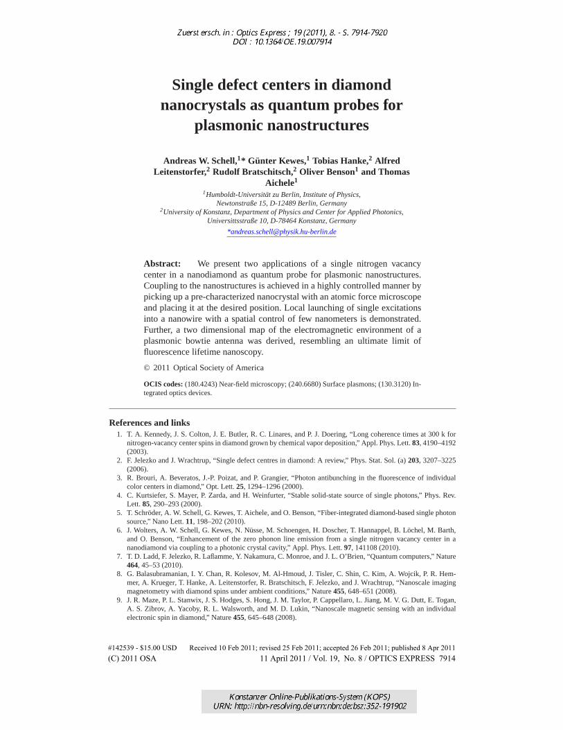
Figure 1(b) shows an AFM image of the nanowire, which has a diameter of ≈ 80 nm. Asharp bend separates the nanowire into two arms of 1.9 µm and 0.7 µm length. Under contin-uous wave laser excitation of the NV center (at a wavelenght of 532 nm), photoluminescencedirectly from the diamond nanocrystal (position 2 in Fig. 1(c)) as well as light emerging fromthe bend and from the ends of the nanowire (positions 1 and 3 in Fig. 1(c)) are visible. Sincethere is a strong fluorescence background emerging from the bend of the nanowire while excit-ing the diamond, for further measurements the diamond was placed at another position, so thatthe nanowire bend is no longer in the excitation spot (position 2 in Fig. 2(c)). Already this repo-sitioning of the nanocrystal shows the advantage of nanomanipulation. Accidental inconvenientconfigurations can be corrected and experiments can be repeated under otherwise unchangedconditions. At the same time, the ability to reposition is crucial in more complex structures,since slight changes of the position of an emitter with respect to a plasmonic structure mayalready modify its emission as well as the structures plasmonic properties significantly. Despitethe possibility to perform near-field simulations, under experimental conditions an a priori pre-diction of an optimum position for an emitter or nanoprobe is often impossible [23].
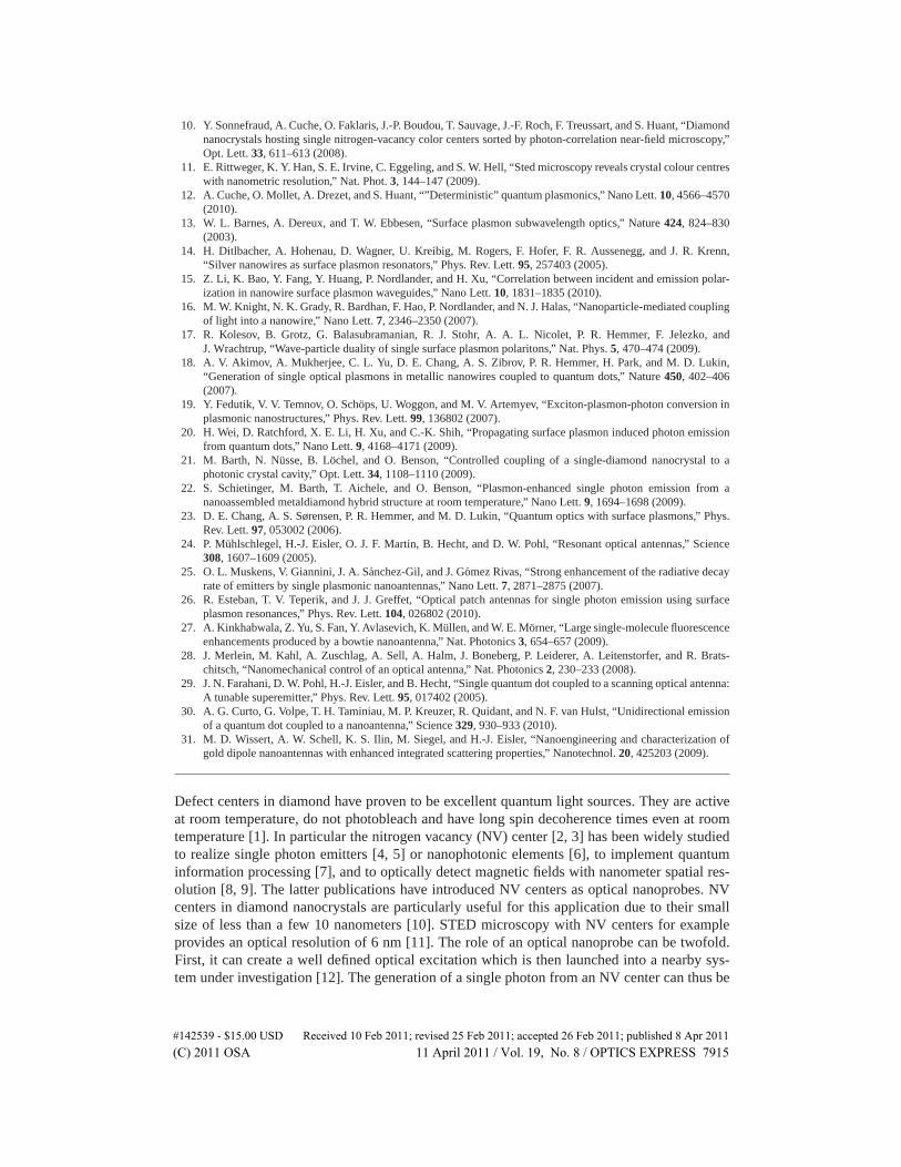
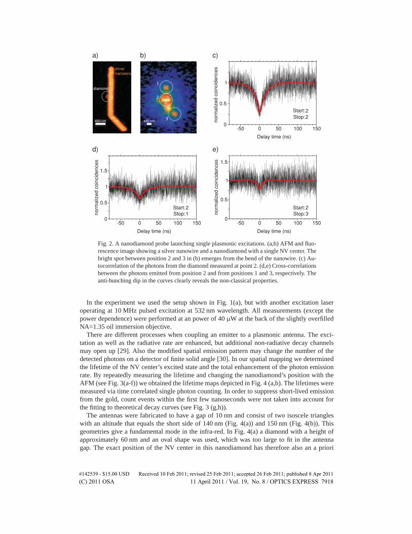
With the new position of the diamond nanocrystal there are now four fluorescent spots ob-servable on the nanowire. One (position 2 in Fig. 2(b)) corresponds to the emission of fluo-
#142539 - $15.00 USD Received 10 Feb 2011; revised 25 Feb 2011; accepted 26 Feb 2011; published 8 Apr 2011(C) 2011 OSA 11 April 2011 / Vol. 19, No. 8 / OPTICS EXPRESS 7916
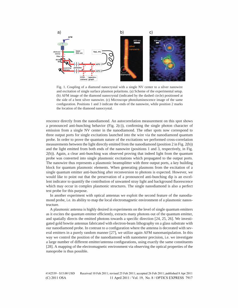
Fig. 1. Coupling of a diamond nanocrystal with a single NV center to a silver nanowireand excitation of single surface plasmon polaritons. (a) Scheme of the experimental setup.(b) AFM image of the diamond nanocrystal (indicated by the dashed circle) positioned atthe side of a bent silver nanowire. (c) Microscope photoluminescence image of the sameconfiguration. Positions 1 and 3 indicate the ends of the nanowire, while position 2 marksthe location of the diamond nanocrystal.
rescence directly from the nanodiamond. An autocorrelation measurement on this spot showsa pronounced anti-bunching behavior (Fig. 2(c)), confirming the single photon character ofemission from a single NV center in the nanodiamond. The other spots now correspond tothree output ports for single excitations launched into the wire via the nanodiamond quantumprobe. In order to prove the quantum nature of the excitations we performed cross-correlationmeasurements between the light directly emitted from the nanodiamond (position 2 in Fig. 2(b))and the light emitted from both ends of the nanowire (positions 1 and 3, respectively, in Fig.2(b)). Again, a clear anti-bunching was observed proving that indeed light from the quantumprobe was converted into single plasmonic excitations which propagated to the output ports.The nanowire thus represents a plasmonic beamsplitter with three output ports, a key buildingblock for quantum plasmonic elements. When generating plasmons from the excitation of asingle quantum emitter anti-bunching after reconversion to photons is expected. However, wewould like to point out that the preservation of a pronounced anti-bunching dip is an excel-lent indicator to quantify the contribution of unwanted stray light and background fluorescencewhich may occur in complex plasmonic structures. The single nanodiamond is also a perfecttest probe for this purpose.
In another experiment with optical antennas we exploit the second feature of the nanodia-mond probe, i.e. its ability to map the local electromagnetic environment of a plasmonic nanos-tructure.
A plasmonic antenna is highly desired in experiments on the level of single quantum emittersas it excites the quantum emitter efficiently, extracts many photons out of the quantum emitter,and spatially directs the emitted photons towards a specific direction [24, 25, 26]. We investi-gated gold bowtie antennas fabricated with electron-beam lithography on a glass substrate withour nanodiamond probe. In contrast to a configuration where the antenna is decorated with sev-eral emitters in a purely random manner [27], we utilize again AFM nanomanipulation. In thisway we control the position of the nanodiamond with nanometer precision, i.e. we investigatea large number of different emitter/antenna configurations, using exactly the same constituents[28]. A mapping of the electromagnetic environment via observing the optical properties of thenanoprobe is thus possible.
#142539 - $15.00 USD Received 10 Feb 2011; revised 25 Feb 2011; accepted 26 Feb 2011; published 8 Apr 2011(C) 2011 OSA 11 April 2011 / Vol. 19, No. 8 / OPTICS EXPRESS 7917
1
3
2
Fig. 2. A nanodiamond probe launching single plasmonic excitations. (a,b) AFM and fluo-rescence image showing a silver nanowire and a nanodiamond with a single NV center. Thebright spot between position 2 and 3 in (b) emerges from the bend of the nanowire. (c) Au-tocorrelation of the photons from the diamond measured at point 2. (d,e) Cross-correlationsbetween the photons emitted from position 2 and from positions 1 and 3, respectively. Theanti-bunching dip in the curves clearly reveals the non-classical properties.
In the experiment we used the setup shown in Fig. 1(a), but with another excitation laseroperating at 10 MHz pulsed excitation at 532 nm wavelength. All measurements (except thepower dependence) were performed at an power of 40 µW at the back of the slightly overfilledNA=1.35 oil immersion objective.
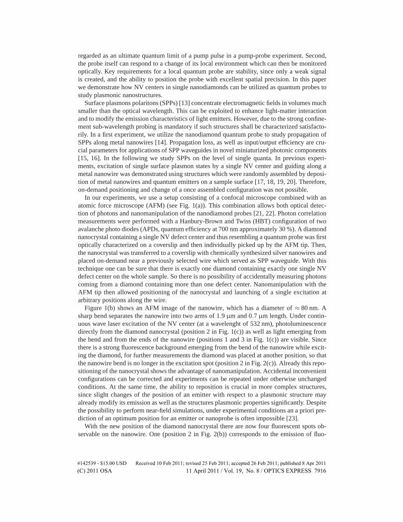
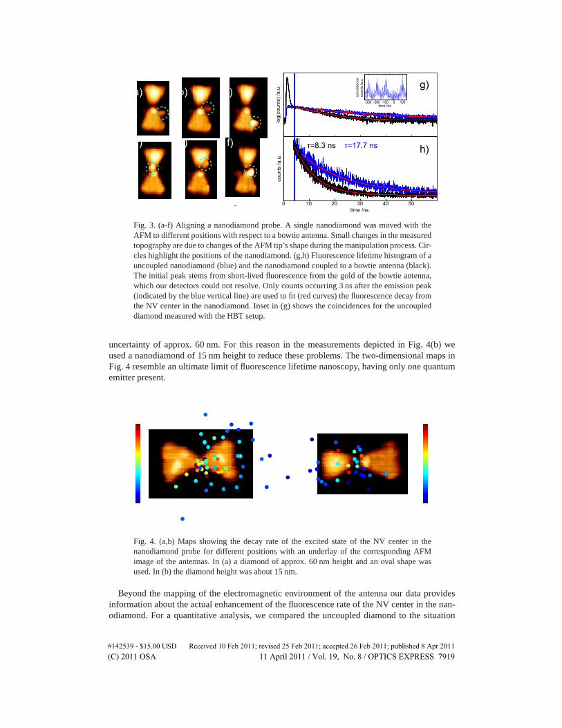
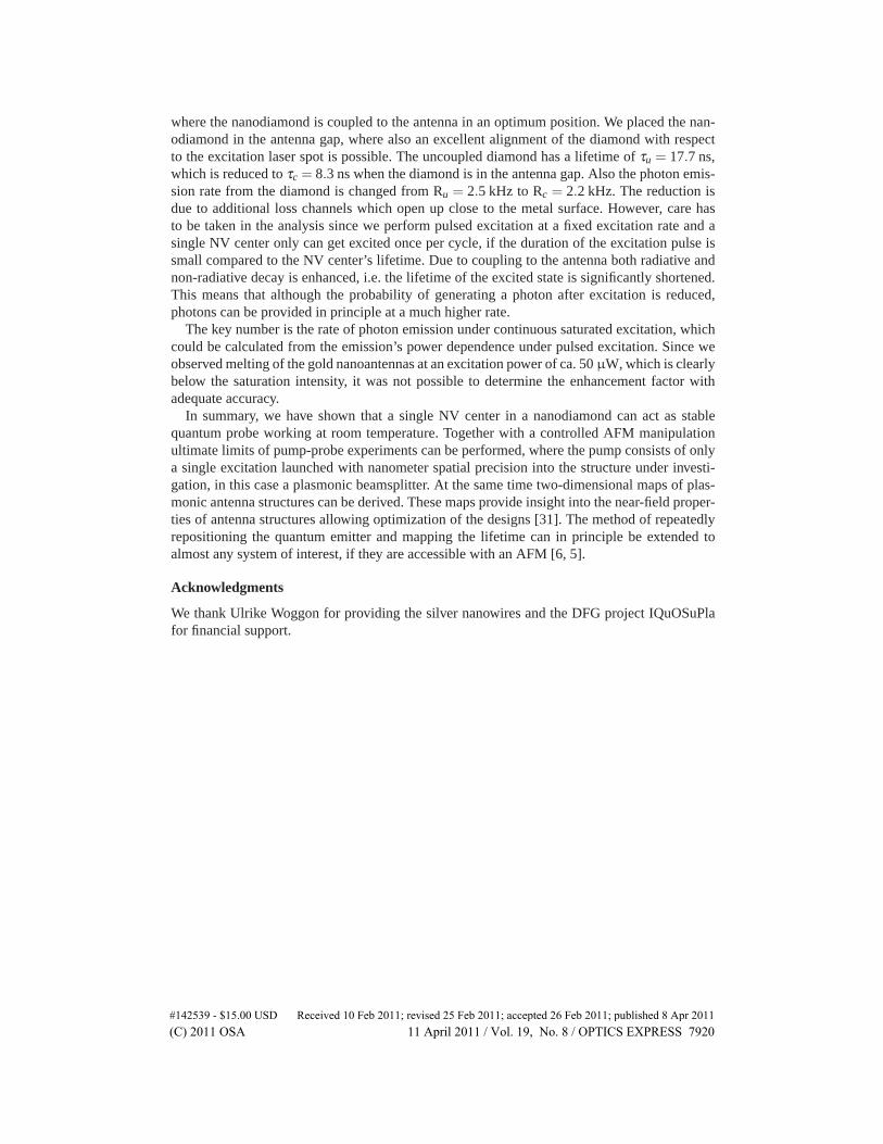
There are different processes when coupling an emitter to a plasmonic antenna. The exci-tation as well as the radiative rate are enhanced, but additional non-radiative decay channelsmay open up [29]. Also the modified spatial emission pattern may change the number of thedetected photons on a detector of finite solid angle [30]. In our spatial mapping we determinedthe lifetime of the NV center’s excited state and the total enhancement of the photon emissionrate. By repeatedly measuring the lifetime and changing the nanodiamond’s position with theAFM (see Fig. 3(a-f)) we obtained the lifetime maps depicted in Fig. 4 (a,b). The lifetimes weremeasured via time correlated single photon counting. In order to suppress short-lived emissionfrom the gold, count events within the first few nanoseconds were not taken into account forthe fitting to theoretical decay curves (see Fig. 3 (g,h)).
The antennas were fabricated to have a gap of 10 nm and consist of two isoscele triangleswith an altitude that equals the short side of 140 nm (Fig. 4(a)) and 150 nm (Fig. 4(b)). Thisgeometries give a fundamental mode in the infra-red. In Fig. 4(a) a diamond with a height ofapproximately 60 nm and an oval shape was used, which was too large to fit in the antennagap. The exact position of the NV center in this nanodiamond has therefore also an a priori
#142539 - $15.00 USD Received 10 Feb 2011; revised 25 Feb 2011; accepted 26 Feb 2011; published 8 Apr 2011(C) 2011 OSA 11 April 2011 / Vol. 19, No. 8 / OPTICS EXPRESS 7918
a) b) c)
d) e) f)
200 nm 0 10 20 30 40 50
coun
ts /a
.u.
time /ns
log(
coun
ts) /
a.u. g)
h)τ=8.3 ns τ=17.7 ns
-300 -200 -100 0 1000
coin
cide
nce
coun
ts /a
.u.
time /ns
Fig. 3. (a-f) Aligning a nanodiamond probe. A single nanodiamond was moved with theAFM to different positions with respect to a bowtie antenna. Small changes in the measuredtopography are due to changes of the AFM tip’s shape during the manipulation process. Cir-cles highlight the positions of the nanodiamond. (g,h) Fluorescence lifetime histogram of auncoupled nanodiamond (blue) and the nanodiamond coupled to a bowtie antenna (black).The initial peak stems from short-lived fluorescence from the gold of the bowtie antenna,which our detectors could not resolve. Only counts occurring 3 ns after the emission peak(indicated by the blue vertical line) are used to fit (red curves) the fluorescence decay fromthe NV center in the nanodiamond. Inset in (g) shows the coincidences for the uncoupleddiamond measured with the HBT setup.
uncertainty of approx. 60 nm. For this reason in the measurements depicted in Fig. 4(b) weused a nanodiamond of 15 nm height to reduce these problems. The two-dimensional maps inFig. 4 resemble an ultimate limit of fluorescence lifetime nanoscopy, having only one quantumemitter present.
27/µs
118/µs 175/µs
30/µs
a) b)
100 nm 100 nm
Fig. 4. (a,b) Maps showing the decay rate of the excited state of the NV center in thenanodiamond probe for different positions with an underlay of the corresponding AFMimage of the antennas. In (a) a diamond of approx. 60 nm height and an oval shape wasused. In (b) the diamond height was about 15 nm.
Beyond the mapping of the electromagnetic environment of the antenna our data providesinformation about the actual enhancement of the fluorescence rate of the NV center in the nan-odiamond. For a quantitative analysis, we compared the uncoupled diamond to the situation
#142539 - $15.00 USD Received 10 Feb 2011; revised 25 Feb 2011; accepted 26 Feb 2011; published 8 Apr 2011(C) 2011 OSA 11 April 2011 / Vol. 19, No. 8 / OPTICS EXPRESS 7919
where the nanodiamond is coupled to the antenna in an optimum position. We placed the nan-odiamond in the antenna gap, where also an excellent alignment of the diamond with respectto the excitation laser spot is possible. The uncoupled diamond has a lifetime of τu = 17.7 ns,which is reduced to τc = 8.3 ns when the diamond is in the antenna gap. Also the photon emis-sion rate from the diamond is changed from Ru = 2.5 kHz to Rc = 2.2 kHz. The reduction isdue to additional loss channels which open up close to the metal surface. However, care hasto be taken in the analysis since we perform pulsed excitation at a fixed excitation rate and asingle NV center only can get excited once per cycle, if the duration of the excitation pulse issmall compared to the NV center’s lifetime. Due to coupling to the antenna both radiative andnon-radiative decay is enhanced, i.e. the lifetime of the excited state is significantly shortened.This means that although the probability of generating a photon after excitation is reduced,photons can be provided in principle at a much higher rate.
The key number is the rate of photon emission under continuous saturated excitation, whichcould be calculated from the emission’s power dependence under pulsed excitation. Since weobserved melting of the gold nanoantennas at an excitation power of ca. 50 µW, which is clearlybelow the saturation intensity, it was not possible to determine the enhancement factor withadequate accuracy.
In summary, we have shown that a single NV center in a nanodiamond can act as stablequantum probe working at room temperature. Together with a controlled AFM manipulationultimate limits of pump-probe experiments can be performed, where the pump consists of onlya single excitation launched with nanometer spatial precision into the structure under investi-gation, in this case a plasmonic beamsplitter. At the same time two-dimensional maps of plas-monic antenna structures can be derived. These maps provide insight into the near-field proper-ties of antenna structures allowing optimization of the designs [31]. The method of repeatedlyrepositioning the quantum emitter and mapping the lifetime can in principle be extended toalmost any system of interest, if they are accessible with an AFM [6, 5].
Acknowledgments
We thank Ulrike Woggon for providing the silver nanowires and the DFG project IQuOSuPlafor financial support.
#142539 - $15.00 USD Received 10 Feb 2011; revised 25 Feb 2011; accepted 26 Feb 2011; published 8 Apr 2011(C) 2011 OSA 11 April 2011 / Vol. 19, No. 8 / OPTICS EXPRESS 7920