Embed Size (px)
Citation preview
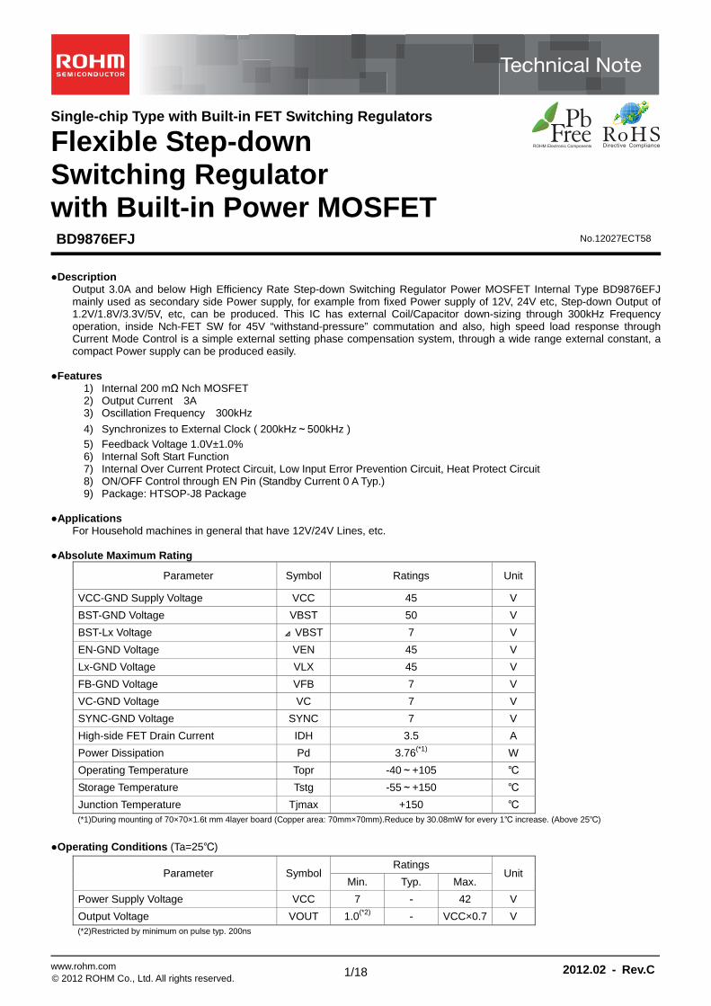
1/18 www.rohm.com 2012.02 - Rev.C© 2012 ROHM Co., Ltd. All rights reserved.
Single-chip Type with Built-in FET Switching Regulators
Flexible Step-down Switching Regulator with Built-in Power MOSFET BD9876EFJ Description
Output 3.0A and below High Efficiency Rate Step-down Switching Regulator Power MOSFET Internal Type BD9876EFJ mainly used as secondary side Power supply, for example from fixed Power supply of 12V, 24V etc, Step-down Output of 1.2V/1.8V/3.3V/5V, etc, can be produced. This IC has external Coil/Capacitor down-sizing through 300kHz Frequency operation, inside Nch-FET SW for 45V “withstand-pressure” commutation and also, high speed load response through Current Mode Control is a simple external setting phase compensation system, through a wide range external constant, a compact Power supply can be produced easily.
Features 1) Internal 200 mΩ Nch MOSFET 2) Output Current 3A 3) Oscillation Frequency 300kHz 4) Synchronizes to External Clock ( 200kHz~500kHz ) 5) Feedback Voltage 1.0V±1.0% 6) Internal Soft Start Function 7) Internal Over Current Protect Circuit, Low Input Error Prevention Circuit, Heat Protect Circuit 8) ON/OFF Control through EN Pin (Standby Current 0 A Typ.) 9) Package: HTSOP-J8 Package
Applications For Household machines in general that have 12V/24V Lines, etc.
Absolute Maximum Rating
Parameter Symbol Ratings Unit
VCC-GND Supply Voltage VCC 45 V BST-GND Voltage VBST 50 V BST-Lx Voltage ⊿ VBST 7 V EN-GND Voltage VEN 45 V Lx-GND Voltage VLX 45 V FB-GND Voltage VFB 7 V VC-GND Voltage VC 7 V SYNC-GND Voltage SYNC 7 V High-side FET Drain Current IDH 3.5 A Power Dissipation Pd 3.76(*1) W Operating Temperature Topr -40~+105 Storage Temperature Tstg -55~+150 Junction Temperature Tjmax +150 (*1)During mounting of 70×70×1.6t mm 4layer board (Copper area: 70mm×70mm).Reduce by 30.08mW for every 1 increase. (Above 25)
Operating Conditions (Ta=25)
Parameter SymbolRatings
Unit Min. Typ. Max.
Power Supply Voltage VCC 7 - 42 V Output Voltage VOUT 1.0(*2) - VCC×0.7 V (*2)Restricted by minimum on pulse typ. 200ns
No.12027ECT58

Technical Note
2/18 www.rohm.com 2012.02 - Rev.C© 2012 ROHM Co., Ltd. All rights reserved.
BD9876EFJ
Electrical Characteristics (Unless otherwise specified, Ta=25, VCC=24V, Vo=5V,EN=3V)
Parameter SymbolLimits
Unit Conditions Min. Typ. Max.
【Circuit Current】
Stand-by current of VCC Ist - 0 10 µA VEN=0V
Circuit current of VCC Icc - 1 2 mA FB=1.2V
【Under Voltage Lock Out (UVLO)】
Detect Voltage Vuv 6.1 6.4 6.7 V
Hysteresis width Vuvhy - 200 300 mV 【Oscillator】
Oscillating frequency fosc 270 300 330 kHz
Max Duty Cycle Dmax 85 91 97 % 【Error Amp】
FB threshold voltage VFB 0.990 1.000 1.010 V
Input bias current IFB -1.0 0 1.0 µA VFB=0V
Error amplifier DC gain AVEA 700 7000 70000 V/V
Trans Conductance GEA 110 220 440 µA/V IVC=±10µA, VC=1.5V
Soft Start Time Tsoft 7 10 13 ms 【Current Sense Amp】
VC to switch current transconductance GCS 5 10 20 A/V 【Output】
Lx NMOS ON resistance RonH - 200 340 mΩ
Lx pre-charge NMOS ON resistance RonL - 10 17 Ω
Over Current Detect Current Iocp 3.5 6 - A 【CTL】
EN Pin Control voltage ON VENON 2 - VCC V OFF VENOFF -0.3 - 0.8 V
EN Pin input current REN 2.7 5.5 11 µA VEN=3V
【SYNC】
SYNC Pin Control voltage High VSYNCH 2.0 - 5.5 V Low VSYNCL -0.3 - 0.8 V
SYNC Pin input current REN 6 12 24 µA VSYNC=3V
SYNC falling edge to LX rising edge delay tdelay 200 400 600 ns Not designed to withstand radiation.

Technical Note
3/18 www.rohm.com 2012.02 - Rev.C© 2012 ROHM Co., Ltd. All rights reserved.
BD9876EFJ
Pin Description Pin No.
Pin Name Function
1 Lx Terminal for inductor
2 GND Ground pin
3 VC Error amplifier output
4 FB Inverting node of the trans conductance error amplifier
5 SYNC Input pin of an external signal for the device synchronized by external signal
6 EN Stand-by ON/OFF pin
7 BST Voltage Supply pin for High Side FET Driver
8 VCC Voltage input pin
Block Diagram
1 2 3 4
8 7 6 5
Thermal Pad
Fig.1 Pin Layout Diagram
Fig.2 Block Diagram
EN
1.0V
Error AMP
C
LX
ReferenceUVLO
VREF
REG
200mΩ
Soft Start
ON/OFF
GND
+-+
FBBST
TSD
Shutdown
10Ω
VC
R QS
CurrentComparator
VOUT
SYNC
Oscillator 300kHz
Σ + -
CurrentSense AMP

Technical Note
4/18 www.rohm.com 2012.02 - Rev.C© 2012 ROHM Co., Ltd. All rights reserved.
BD9876EFJ
Block Description 1. Reference
This Block generates Error Amp Standard Voltage. Standard Voltage is 1.0V.
2. REG This is a Gate Drive Voltage Generator and 5V Low Saturation regulator for internal Circuit Power supply.
3. OSC This is a precise wave Oscillation Circuit with Operation Frequency fixed to 300 kHz fixed (self-running mode). To implement the synchronization feature connect a square wave (Hi Level: higher than 2V Low Level: lower than 0.8V ) to the SYNC pin. The synchronization frequency range is 200 kHz to 500 kHz. After connecting the rising edge of LX will be synchronized to the falling edge of SYNC pin signal after 3 count. At the synchronization remove the external clock, the device transitions self-running mode after 7 microseconds.
4. Soft Start A Circuit that does Soft Start to the Output Voltage of DC/DC Comparator, and prevents Rush Current during Start-up. Soft Start Time is set at IC internal, after 10ms from starting-up EN Pin, Standard Voltage comes to 1.0V, and Output Voltage becomes set Voltage.
5. ERROR AMP This is an Error amplifier what detects Output Signal, and outputs PWM Control Signal. Internal Standard Voltage is set to 1.0V. Also, C and R are connected between the Output (VC) Pin GND of Error Amp as Phase compensation elements. (See P.11)
6. ICOMP This is a Voltage-Pulse Width Converter that controls Output Voltage in response to Input Voltage. This compares the Voltage added to the internal SLOPE waveform in response to the FET WS Current with Error amplifier Output Voltage, controls the width of Output Pulse and outputs to Driver.
7. Nch FET SW This is an internal commutation SW that converts Coil Current of DC/DC Comparator. It contains 45V” with stand pressure” 200mΩ SW. Because the Current Rating of this FET is 3.5A included ripple current, please use at within 3.5A. The device has the circuit of over current protection for protecting the FET from over current. To detect OCP 2 times sequentially, the device will stop and after 13 msec restart.
8. UVLO This is a Low Voltage Error Prevention Circuit. This prevents internal circuit error during increase of Power supply Voltage and during decline of Power supply Voltage. It monitors VCC Pin Voltage and internal REG Voltage, And when VCC Voltage becomes 6.4V and below, it turns OFF all Output FET and turns OFF DC/DC Comparator Output, and Soft Start Circuit resets. Now this Threshold has Hysteresis of 200mV.
9. TSD This is a Heat Protect (Temperature Protect) Circuit. When it detects an abnormal temperature exceeding Maximum Junction Temperature (Tj=150), it turns OFF all Output FET, and turns OFF DC/DC Comparator Output. When Temperature falls, it has/with Hysteresis and automatically returns.
10. EN With the Voltage applied to EN Pin(6pin), IC ON/OFF can be controlled. When a Voltage of 2.0V or more is applied, it turns ON, at Open or 0V application, it turns OFF. About 550kΩ Pull-down Resistance is contained within the Pin.

Technical Note
5/18 www.rohm.com 2012.02 - Rev.C© 2012 ROHM Co., Ltd. All rights reserved.
BD9876EFJ
Detailed Description Synchronizes to External Clock
The SYNC pin can be used to synchronize the regulator to an external system clock. To implement the synchronization feature connect a square wave to SYNC pin. The square wave amplitude must transition lower than 0.8V and higher than 2.0V on the SYNC pin and have an on time greater than 100ns and an off time greater than 100ns. The synchronization frequency range is 200 kHz to 500 kHz. The rising edge of the LX will be synchronized to the falling edge of SYNC pin signal after SYNC input pulse 3 count. At the synchronization, the external clock is removed, the device transitions self-running mode after 7 microseconds.
The case of not using the function of synchronization
Although the SYNC pin is pulled down by resistor in this
device, if the function of the synchronization is not used , it is recommended to connect SYNC pin to ground.
SOFT START
The soft start time of BD9876EFJ is determined by the DCDC operating frequency (self-run mode 300 kHz ⇒ 10ms). If synchronization is used at the time of EN=ON, The soft start time is restricted by SYNC pin input pulse frequency. SYNC pin input pulse frequency is fosc_ex kHz, the soft start time is expressed by below equation.
Fig.3 Timing chart at Synchronization
fosc_ex
300 Tss = × 10 [ms]
SYNC
SYNC_LATCH
Lx
Set the latch for synchronization
400nsec
about 7µsec
Fig.4 the method to disposal the SYNC pin without synchronization

Technical Note
6/18 www.rohm.com 2012.02 - Rev.C© 2012 ROHM Co., Ltd. All rights reserved.
BD9876EFJ
OCP operation The device has the circuit of over current protection for protecting the FET from over current. To detect OCP 2 times sequentially, the device will stop and after 13 msec restart.
OCP operation at soft start BD9876EFJ have the function to change the OCP reference voltage according to slope for soft start to prevent IC from abnormal current at higher input voltage. This function restricts the OCP threshold a half of the specification value (typ.3A).
Fig.5 Timing chart at OCP operation
VC
Lx
VOUT
OCP
OCP_LATCH
set the OCP latch by detectingthe OCP current 2 times sequencially
output connect to GND
OCP latch reset after 13 msec(300kHz 4000 counts)
force the High side FET OFF by detecting OCP current(pulse by pulse protection)
VC voltage discharged by OCP latchOCP threshold
VC voltage rising byoutput connect to GND
Fig.6 the relation SS node voltage and OCP reference voltage.
Technical Note
7/18 www.rohm.com 2012.02 - Rev.C© 2012 ROHM Co., Ltd. All rights reserved.
BD9876EFJ
0
0.1
0.2
0.3
0.4
0.5
0.6
0.7
0.8
0.9
1
-60 -40 -20 0 20 40 60 80 100 120
ICC[uA
]
Temp[ ]
VCC=12V
VCC=24V
VCC=36V
VCC=42V
0
0.5
1
1.5
2
-60 -40 -20 0 20 40 60 80 100 120
ICC[mA]
Temp[ ]
VCC=42V
VCC=36V
VCC=24V
VCC=12V
0
0.5
1
1.5
2
0 5 10 15 20 25 30 35 40 45
ICC[mA]
VCC[V]
Temp=‐40
Temp=25
Temp=105
250
260
270
280
290
300
310
320
330
340
350
-60 -40 -20 0 20 40 60 80 100 120
FREQ
UEN
CY[kHz]
Temp[ ]
0
1
2
3
4
5
6
7
8
-60 -40 -20 0 20 40 60 80 100 120
UVLO
threshold[V]
Temp[ ]
reset voltage
detect voltage
0
10
20
30
40
50
60
70
80
90
100
-60 -40 -20 0 20 40 60 80 100 120MAXD
UTY[%
]Temp[ ]
0.990
0.992
0.994
0.996
0.998
1.000
1.002
1.004
1.006
1.008
1.010
-60 -40 -20 0 20 40 60 80 100 120
VFB
threshold[V]
Temp[ ]
VCC=12VVCC=24V
VCC=42VVCC=36V
0.990
0.992
0.994
0.996
0.998
1.000
1.002
1.004
1.006
1.008
1.010
0 5 10 15 20 25 30 35 40 45
VFB
threshold[V]
VCC[V]
Temp=105Temp=25
Temp=‐40
‐60‐50‐40‐30‐20‐100
102030405060
0 0.5 1 1.5 2
VC term
inal current[uA]
VFB[V]
Temp=105
Temp=25
Temp=‐40
Reference Data (Unless otherwise specified, Ta=25, VCC=24V, Vo=5V, EN=3V)
Fig.14. FB Threshold Power supply Characteristics
Fig.13. FB Threshold Voltage Temperature Characteristics
Fig.15. FB Voltage - IVC Current Characteristics
Fig.11. Oscillation Frequency Temperature Characteristics
Fig.10. UVLO Threshold Temperature Characteristics
Fig.12. Max Duty Temperature Characteristics
Fig.7. Standby Current Temperature Characteristics
Fig.9. Circuit Current Temperature Characteristics
Fig.8. Circuit Current Power supply Voltage Characteristics

Technical Note
8/18 www.rohm.com 2012.02 - Rev.C© 2012 ROHM Co., Ltd. All rights reserved.
BD9876EFJ
0
5
10
15
20
-60 -40 -20 0 20 40 60 80 100 120
PRECHARG
E FET RO
N [Ω]
Temp[ ]
0
50
100
150
200
250
300
-60 -40 -20 0 20 40 60 80 100 120
HIGHSIDE FET RO
N [m
Ω]
Temp[ ]
0
2
4
6
8
10
12
14
16
-60 -40 -20 0 20 40 60 80 100 120
Soft Start Tim
e[ms]
Temp[ ]
VCC=42V
VCC=36V
VCC=24V
VCC=12V
0123456789
1011121314
-60 -40 -20 0 20 40 60 80 100 120
VC to SW Current
transcon
ductance[A/V
]
Temp[ ]
0
0.5
1
1.5
2
-60 -40 -20 0 20 40 60 80 100 120EN
Thresho
ld[V]
Temp[ ]
0
1
2
3
4
5
6
7
8
9
10
-60 -40 -20 0 20 40 60 80 100 120
OCP
_detect_curren
t[A]
Temp[ ]
VCC=12V
VCC=24VVCC=36V
VCC=42V
Fig.19 OCP Detect Current Temperature Characteristics
Fig.16. Soft Start Time Temperature Characteristics
Fig.17. Nch FET ON Resistance Temperature Characteristics
Fig.18. Pre-charge FET ON Resistance Temperature Characteristics
Fig.20. VC to SW current transconductance Temperature characteristics
Fig.21. EN Threshold Temperature Characteristics

Technical Note
9/18 www.rohm.com 2012.02 - Rev.C© 2012 ROHM Co., Ltd. All rights reserved.
BD9876EFJ
Fig.22 Reference Application Circuit
Fig.29 Stop Waveform
Fig.23 Electric Power Conversion Rate
Fig.25 Frequency Response Characteristics (Io=3.0A)
Fig.24 Frequency Response Characteristics (Io=0.5A)
Phase
Gain
Fig.28 startup Waveform
EN:5V/div (DC) LX:10V/div (DC IL:0.5A/div (DC) VOUT:2V./div (DC)
EN:5V/div (DC) LX:10V/div (DC IL:0.5A/div (DC) VOUT:2V./div (DC)
Fig.26 Load Response Characteristics (Io=0A→3.0A)
Fig.27 Load Response Characteristics (Io=3.0A→0A)
VOUT:200mV/div (AC)
IL:1A/div (DC)
VOUT:200mV/div (AC)
IL:1A/div (DC)
0
10
20
30
40
50
60
70
80
90
100
0 500 1000 1500 2000 2500 3000
Transformation Efficiency η[%]
LOAD CURRENT[mA]
VCC=12V
VCC=24VVCC=36V
VCC=42V
Phase
Gain
Example of Reference Application Circuit (Input 24V, Output 5.0V/ 2.5A) Reference Application Data (Example of Reference Application Circuit)
VCC 24VVOUT
C1 6800pF
EN
Lx
GND
VC
FB
VCC
BST
EN
SYNC SYNC
10µF/35VGRM31EB3YA106KA12L(murata)47µF/15V
GRM32EB31C476KE15 (murata)
RB056L-40 (ROHM)
15µH CDRH105R(SUMIDA)
0.01µF
R3 10kΩR2 30kΩ
R1 120kΩ
ON/OFFcontrol
5V/2.5A

Technical Note
10/18 www.rohm.com 2012.02 - Rev.C© 2012 ROHM Co., Ltd. All rights reserved.
BD9876EFJ
Evaluation Board Pattern (Reference) Layout is a critical portion of good power supply design. There are several signals paths that conduct fast changing currents or voltages that can interact with stray inductance or parasitic capacitance to generate noise or degrade the power supplies performance. To help eliminate these problems, the VCC pin should be bypassed to ground with a low ESR ceramic bypass capacitor with B dielectric. Care should be taken to minimize the loop area formed by the bypass capacitor connections, the VCC pin, and the anode of the catch diode. See Fig.28 for a PCB layout example. The GND pin should be tied directly to the thermal pad under the IC and the thermal pad. The thermal pad should be connected to any internal PCB ground planes using multiple VIAs directly under the IC. The LX pin should be routed to the cathode of the catch diode and to the output inductor. Since the LX connection is the switching node, the catch diode and output inductor should be located close to the LX pins, and the area of the PCB conductor minimized to prevent excessive capacitive coupling. For operation at full rated load, the top side ground area must provide adequate heat dissipating area. The additional external components can be placed approximately as shown. It may be possible to obtain acceptable performance with alternate PCB layouts, however this layout has been shown to produce good results and is meant as a guideline.
Fig.30 Evaluation Board Pattern
LX
GND
VC
FB
VCC
BST
EN
SYNC
Output Inductor
CatchDiode
OutputCapacitor
Input Bypass Capacitor
CBST
Topside GroundArea
CompensationNetwork
ResistorDivider
VOUT
Route BST CapacitorTrace on another layer toprovide with wide path for topside ground
Signal VIAThermal VIA
VCC

Technical Note
11/18 www.rohm.com 2012.02 - Rev.C© 2012 ROHM Co., Ltd. All rights reserved.
BD9876EFJ
Power Dissipation It is shown below reducing characteristics of power dissipation to mount 70mm×70mm×1.6mmt PCB Junction temperature must be designed not to exceed 150.
Power Dissipation Estimate
The following formulas show how to estimate the device power dissipation under continuous mode operations. They should not be used if the device is working in the discontinuous conduction mode. The device power dissipation includes: 1) Conduction loss: Pcon = IOUT2 × RonH × VOUT/VCC 2) Switching loss: Psw = 1.25 × 10⁻⁹ × VCC2 × IOUT × fsw 3) Gate charge loss: Pgc = 22.8 × 10⁻⁹ × fsw
4) Quiescent current loss: Pq = 1.0 × 10⁻³ × VCC Where: IOUT is the output current (A), RonH is the on-resistance of the high-side MOSFET(Ω), VOUT is the output voltage (V). VCC is the input voltage (V), fsw is the switching frequency (Hz). Therefore Power dissipation of IC is the sum of above dissipation. Pd = Pcon + Psw + Pgc + Pq For given Tj, Tj =Ta + θja × Pd Where: Pd is the total device power dissipation (W), Ta is the ambient temperature ()
Tj is the junction temperature (), θja is the thermal resistance of the package ()
Fig.31 Power Dissipation ( 70mm×70mm×1.6mmt 1layer PCB)
0
500
1000
1500
2000
2500
3000
3500
4000
0 25 50 75 100 125 150
POW
ER D
ISSI
PATI
ON
-m
W
Ambient Temperature -
④3760mW
③2210mW
②1100mW
HTSOP-J8 Package -
On 70mm×70mm×1.6mmt glass epoxy PCB
①1-layer board (Backside copper foil area 0mm×0mm)
②2-layer board ( Backside copper foil area 15mm×15mm)
③2-layer board (Backside copper foil area 70mm×70mm)
④4-layer board (Backside copper foil area 70mm×70mm)
①820mW

Technical Note
12/18 www.rohm.com 2012.02 - Rev.C© 2012 ROHM Co., Ltd. All rights reserved.
BD9876EFJ
ESRRILCOUTf
×∆+××
×∆=π2
1ILVpp
max_21min_
fcRlOUT
××=
πC
fVCCVOUT
LVOUTVCCIL 1
××−
=∆
2ILIOUTIpeak ∆
+=
221
RRRVOUT +
=
Application Components Selection Method (1) Inductor
Something of the shield Type that Fulfills the Current Rating (Current value Ipeak below), with low DCR (Direct Current Resistance element) is recommended. Value of Inductor influences Inductor Ripple Current and becomes the cause of Output Ripple. In the same way as the formula below, this Ripple Current can be made small for as big as the L value of Coil or as high as the Switching Frequency. I
(IL: Output Ripple Current, f: Switching Frequency) For design value of Inductor Ripple Current, please carry out design tentatively with about 20%~50% of Maximum Input Current. ※When current that exceeds Coil rating flows to the coil, the Coil causes a Magnetic Saturation, and there are cases
wherein a decline in efficiency, oscillation of output happens. Please have sufficient margin and select so that Peak Current does not exceed Rating Current of Coil.
(2) Output Capacitor
In order for capacitor to be used in output to reduce output ripple, Low ceramic capacitor of ESR is recommended. Also, for capacitor rating, on top of putting into consideration DC Bias characteristics, please use something whose maximum rating has sufficient margin with respect to the Output Voltage. Output ripple voltage is looked for using the following formula. The actual value of the output capacitor is not critical, but some practical limits do exist. Consider the relationship between the crossover frequency of the design and LC corner frequency of the output filter. In general, it is desirable to keep the crossover frequency at less than 1/5 of the switching frequency. With high switching frequencies such as the 600kHz frequency of this design, internal circuit limitations of the BD9675FJ limit the practical maximum crossover frequency to about 30kHz. In general, the crossover frequency should be higher than the corner frequency determined by the load impedance and the output capacitor. This limits the minimum capacitor value for the output filter to: Where: Rl is the output load resistance and fc_max is the maximum crossover frequency. The output ripple voltage can be estimated by: . Please design in a way that it is held within Capacity Ripple Voltage.
(3) Output Voltage Setting ERROR AMP internal Standard Voltage is 1.0V. Output Voltage is determined as seen in (4) formula.
(4) Bootstrap Capacitor Please connect from 4700pF to 22000pF (Laminate Ceramic Capacitor) between BST Pin and Lx Pin.
ΔIL
Fig.32 Inductor Current
Fig. 33Voltage Return Resistance Setting Method
VREF 1.0V
VOUT
ERROR AMP R1
R2
FB
・・・ (3)
・・・ (4)
・・・ (1)
・・・ (2)
・・・ (5)

Technical Note
13/18 www.rohm.com 2012.02 - Rev.C© 2012 ROHM Co., Ltd. All rights reserved.
BD9876EFJ
)VCC
VOUT(1VCC
VOUTIOUTICVCC −××=
2IOUTICVCC_max =
⎥⎦⎤
⎢⎣⎡××
×=∆
VCCVOUT-1
VCCVOUT
CVCCfIOUTVCC
(5) Catch Diode The BD9876EFJ is designed to operate using an external catch diode between Lx and GND. The selected diode must meet the absolute maximum ratings for the application: Reverse voltage must be higher than the maximum voltage at the Lx pin, which is VCC MAX + 0.5 V. Peak current must be greater than IOUTMAX plus on half the peak to peak inductor current.
(6) Input Capacitor
The BD9876EFJ requires an input capacitor and depending on the application. Use low ESR capacitors for the best performance. Ceramic capacitors are preferred, but low-ESR electrolytic capacitors may also suffice. The typical recommended value for the decoupling capacitor is 10uF. Please place this capacitor as possible as close to the VCC pin. When using ceramic capacitors, make sure that they have enough capacitance to provide sufficient charge to prevent excessive voltage ripple at input. The input voltage ripple caused by capacitance can be estimated by: Since the input capacitor (CVCC) absorbs the input switching current it requires an adequate ripple current rating. The RMS current in the input capacitor can be estimated by: The worst case condition occurs at VCC = 2VOUT, where
(7) About Adjustment of DC/DC Comparator Frequency Characteristics Role of Phase compensation element C1, C2, R3 (See P.7. Example of Reference Application Circuit) Stability and Responsiveness of Loop are controlled through VC Pin which is the output of Error Amp. The combination of zero and pole that determines Stability and Responsiveness is adjusted by the combination of resistor and capacitor that are connected in series to the VC Pin. DC Gain of Voltage Return Loop can be calculated for using the following formula. Here, VFB is Feedback Voltage (1.0V).AEA is Voltage Gain of Error amplifier (typ: 77dB), Gcs is the Trans-conductance of Current Detect (typ: 10A/V), and Rl is the Output Load Resistance value. There are 2 important poles in the Control Loop of this DC/DC. The first occurs with/ through the output resistance of Phase compensation Capacitor (C1) and Error amplifier. The other one occurs with/through the Output Capacitor and Load Resistor. These poles appear in the frequency written below. Here, GEA is the trans-conductance of Error amplifier (typ: 220 µA/V). Here, in this Control Loop, one zero becomes important. With the zero which occurs because of Phase compensation Capacitor C1 and Phase compensation Resistor R3, the Frequency below appears. Also, if Output Capacitor is big, and that ESR (RESR) is big, in this Control Loop, there are cases when it has an important, separate zero (ESR zero). This ESR zero occurs due to ESR of Output Capacitor and Capacitance, and exists in the Frequency below. (ESR zero)
VOUTV
AGCSRlAdc FB
EA ×××=
EA
EA
AC12 G1fp
××=
π
RlCOUT2 1
fp2××
=π
R3C12
11fz
××=
π
RESRCOUT2 1
fzESR××
= π
・・・ (7)
・・・ (8)
・・・ (9)
・・・ (10)
・・・ (11)
・・・ (12)
・・・ (13)
・・・ (6)

Technical Note
14/18 www.rohm.com 2012.02 - Rev.C© 2012 ROHM Co., Ltd. All rights reserved.
BD9876EFJ
R3C22
13fp
××=
π
In this case, the 3rd pole determined with the 2nd Phase compensation Capacitor (C2) and Phase Correction Resistor (R3) is used in order to correct the ESR zero results in Loop Gain. This pole exists in the frequency shown below. (Pole that corrects ESR zero) The target of Phase compensation design is to create a communication function in order to acquire necessary band and Phase margin. Cross-over Frequency (band) at which Loop gain of Return Loop becomes “0” is important. When Cross-over Frequency becomes low, Power supply Fluctuation Response, Load Response, etc worsens. On the other hand, when Cross-over Frequency is too high, instability of the Loop can occur. Tentatively, Cross-over Frequency is targeted to be made 1/20 or below of Switching Frequency.
Selection method of Phase Compensation constant is shown below.
1. Phase Compensation Resistor (R3) is selected in order to set to the desired Cross-over Frequency.
Calculation of RC is done using the formula below. Here, fc is the desired Cross-over Frequency. It is made about 1/20 and below of the Normal Switching Frequency (fs).
2. Phase compensation Capacitor (C1) is selected in order to achieve the desired phase margin. In an application that has a representative Inductance value (about several µH~20µH), by matching zero of compensation to 1/4 and below of the Cross-over Frequency, sufficient Phase margin can be acquired. C1 can be calculated using the following formula. RC is Phase compensation Resistor.
3. Examination whether the second Phase compensation Capacitor C2 is necessary or not is done. If the ESR zero of Output Capacitor exists in a place that is smaller than half of the Switching Frequency, a second Phase compensation Capacitor is necessary. In other words, it is the case wherein the formula below happens. In this case, add the second Phase compensation Capacitor C2, and match the frequency of the third pole to the Frequency fp3 of ESR zero.
C2 is looked for using the following formula.
GCSGEA
fcCOUT2×
×
××=
π VFB
VOUTR3
fcR32
4 C1
××π >
2fs
RESRCOUT21
<π ××
R3
RESRCOUTC2
×=
・・・ (14)
・・・ (15)
・・・ (16)
・・・ (17)
・・・ (18)

Technical Note
15/18 www.rohm.com 2012.02 - Rev.C© 2012 ROHM Co., Ltd. All rights reserved.
BD9876EFJ
I/O Equivalent Schematic Pin. No
Pin. Name Pin Equivalent Schematic Pin.
No Pin.
Name Pin Equivalent Schematic
1
2
7
8
Lx
GND
BST
VCC
5 SYNC
3 VC
6 EN
4 FB
BST
VCC
Lx
GND
GND
SYNC
VCC
VC
GND
FB
GND
EN
GND

Technical Note
16/18 www.rohm.com 2012.02 - Rev.C© 2012 ROHM Co., Ltd. All rights reserved.
BD9876EFJ
Notes for use (1) About Absolute Maximum Rating
When the absolute maximum ratings of application voltage, operating temperature range, etc. was exceeded, there is possibility of deterioration and destruction. Also, the short Mode or open mode, etc. destruction condition cannot be assumed. When the special mode where absolute maximum rating is exceeded is assumed, please give consideration to the physical safety countermeasure for the fuse, etc.
(2) About GND Electric Potential
In every state, please make the electric potential of GND Pin into the minimum electrical potential. Also, include the actual excessive effect, and please do it such that the pins, excluding the GND Pin do not become the voltage below GND.
(3) About Heat Design
Consider the Power Dissipation (Pd) in actual state of use, and please make Heat Design with sufficient margin. (4) About short circuit between pins and erroneous mounting
When installing to set board, please be mindful of the direction of the IC, phase difference, etc. If it is not installed correctly, there is a chance that the IC will be destroyed. Also, if a foreign object enters the middle of output, the middle of output and power supply GND, etc., even for the case where it is shorted, there is a change of destruction.
(5) About the operation inside a strong electro-magnetic field
When using inside a strong electro-magnetic field, there is a possibility of error, so please be careful. (6) Temperature Protect Circuit (TSD Circuit)
Temperature Protect Circuit (TSD Circuit) is built-in in this IC. As for the Temperature Protect Circuit (TSD Circuit), because it a circuit that aims to block the IC from insistent careless runs, it is not aimed for protection and guarantee of IC. Therefore, please do not assume the continuing use after operation of this circuit and the Temperature Protect Circuit operation.
(7) About checking with Set boards
When doing examination with the set board, during connection of capacitor to the pin that has low impedance, there is a possibility of stress in the IC, so for every 1 process, please make sure to do electric discharge. As a countermeasure for static electricity, in the process of assembly, do grounding, and when transporting or storing please be careful. Also, when doing connection to the jig in the examination process, please make sure to turn off the power supply, then connect. After that, turn off the power supply then take it off.
(8) About common impedance
For the power supply and the wire of GND, lower the common impedance, then, as much as possible, make the ripple smaller (as much as possible make the wire thick and short, and lower the ripple from L・C), etc., then and please consider it sufficiently.
(9) In the application, when the mode where the VCC and each pin electrical potential becomes reversed exists, there is a
possibility that the internal circuit will become damaged. For example, during cases wherein the condition when charge was given in the external capacitor, and the VCC was shorted to GND, it is recommended to insert the bypass diode to the diode of the back current prevention in the VCC series or the middle of each Pin-VCC.
(10) About High-side Nch FET
Please use within 3.5A contained ripple current, because the absolute maximum rating of high-side Nch FET is 3.5A. (11) About over current detection
The detecting current is the current flowing through high-side Nch FET. Output current containing ripple current, therefore the detecting current is the current of the output current containing ripple current.

Technical Note
17/18 www.rohm.com 2012.02 - Rev.C© 2012 ROHM Co., Ltd. All rights reserved.
BD9876EFJ
(12) About IC Pin Input
This IC is a Monolithic IC, and between each element, it has P+ isolation for element separation and P board. With the N layer of each element and this, the P-N junction is formed, and the parasitic element of each type is composed.
For example, like the diagram below, when resistor and transistor is connected to Pin, When GND>(PinA) in Resistor, when GND>(PinA), when GND>(PinB) in Transistor (NPN),
the P-N junction will operate as a parasitic diode. Also, during GND>(Pin B) in the Transistor (NPN), through the N layer of the other elements connected
to the above-mentioned parasitic diode , the parasitic NPN Transistor will operation. On the composition of IC, depending on the electrical potential, the parasitic element will become necessary. Through the operation of the parasitic element interference of circuit operation will arouse, and error, therefore destruction can be caused. Therefore please be careful about the applying of voltage lower than the GND (P board) in I/O Pin, and the way of using when parasitic element operating.
Fig.34 Example of simple structure of Bipolar IC
~
~
(Pin A)
GND
GND
P Substrate
N
P
N
P+ P+
(Pin A)
Parasitic Element
Resistor
Transistor (NPN)
~
~
GND
N
P
N N
P+ P+
(Pin B)
B
N
E C
GND
N
P Substrate
Parasitic Element
Parasitic Element

Technical Note
18/18 www.rohm.com 2012.02 - Rev.C© 2012 ROHM Co., Ltd. All rights reserved.
BD9876EFJ
Ordering part number
B D 9 8 7 6 E F J - E 2
Part No. Part No. Package EFJ : HTSOP-J8
Packaging and forming specification E2: Embossed tape and reel
(Unit : mm)
HTSOP-J8
0.08 S
0.08 M
S
1.0M
AX
0.85
±0.0
5
1.27
0.08
±0.0
8 0.42+0.05-0.04
1.05
±0.2
0.65
±0.1
5
4°+6°−4°
0.17+0.05-0.03
2 3 4
568
(MAX 5.25 include BURR)
7
1
0.545
(3.2)
4.9±0.1
6.0±
0.2
(2.4
)
3.9±
0.1
1PIN MARK
∗ Order quantity needs to be multiple of the minimum quantity.
<Tape and Reel information>
Embossed carrier tapeTape
Quantity
Direction of feed The direction is the 1pin of product is at the upper left when you hold
reel on the left hand and you pull out the tape on the right hand
2500pcs
E2
( )
Direction of feed
Reel1pin

R1120Awww.rohm.com© 2012 ROHM Co., Ltd. All rights reserved.
Notice
ROHM Customer Support System http://www.rohm.com/contact/
Thank you for your accessing to ROHM product informations. More detail product informations and catalogs are available, please contact us.
N o t e s
No copying or reproduction of this document, in part or in whole, is permitted without the consent of ROHM Co.,Ltd. The content specified herein is subject to change for improvement without notice. The content specified herein is for the purpose of introducing ROHM's products (hereinafter "Products"). If you wish to use any such Product, please be sure to refer to the specifications, which can be obtained from ROHM upon request. Examples of application circuits, circuit constants and any other information contained herein illustrate the standard usage and operations of the Products. The peripheral conditions must be taken into account when designing circuits for mass production. Great care was taken in ensuring the accuracy of the information specified in this document. However, should you incur any damage arising from any inaccuracy or misprint of such information, ROHM shall bear no responsibility for such damage. The technical information specified herein is intended only to show the typical functions of and examples of application circuits for the Products. ROHM does not grant you, explicitly or implicitly, any license to use or exercise intellectual property or other rights held by ROHM and other parties. ROHM shall bear no responsibility whatsoever for any dispute arising from the use of such technical information. The Products specified in this document are intended to be used with general-use electronic equipment or devices (such as audio visual equipment, office-automation equipment, commu-nication devices, electronic appliances and amusement devices). The Products specified in this document are not designed to be radiation tolerant. While ROHM always makes efforts to enhance the quality and reliability of its Products, a Product may fail or malfunction for a variety of reasons. Please be sure to implement in your equipment using the Products safety measures to guard against the possibility of physical injury, fire or any other damage caused in the event of the failure of any Product, such as derating, redundancy, fire control and fail-safe designs. ROHM shall bear no responsibility whatsoever for your use of any Product outside of the prescribed scope or not in accordance with the instruction manual. The Products are not designed or manufactured to be used with any equipment, device or system which requires an extremely high level of reliability the failure or malfunction of which may result in a direct threat to human life or create a risk of human injury (such as a medical instrument, transportation equipment, aerospace machinery, nuclear-reactor controller, fuel-controller or other safety device). ROHM shall bear no responsibility in any way for use of any of the Products for the above special purposes. If a Product is intended to be used for any such special purpose, please contact a ROHM sales representative before purchasing. If you intend to export or ship overseas any Product or technology specified herein that may be controlled under the Foreign Exchange and the Foreign Trade Law, you will be required to obtain a license or permit under the Law.


![Cascode Switching Modeling and Improvement in Flyback ...Cascode GaN FET [10], during inductive hard switching. Figure 2 Cascode Switching Configured Flyback converter II. MODELING](https://img.pdfslide.us/doc/110x75/5e541119f61a9f6e2b2e813c/cascode-switching-modeling-and-improvement-in-flyback-cascode-gan-fet-10.jpg)