Embed Size (px)
Citation preview

1/15 www.rohm.com 2011.02 - Rev.A
© 2011 ROHM Co., Ltd. All rights reserved.
Single-chip Type with Built-in FET Switching Regulators Simple Step-down Switching Regulator with Built-in Power MOSFET BD9328EFJ
Description
The BD9328EFJ is a synchronous step-down switching regulator that integrates 2 low resistance N-channel MOSFETs. It achieves 2A continuous output current over a wide input supply range. Current mode operation provides fast transient response and easy phase compensation.
Features 1) Wide operating INPUT Range 4.2V~18.0V 2) 2A Output Current 3) Hi-side / Lo-side FET ON-resistance; 0.15 / 0.13Ω Power Switch 4) Low ESR Output Ceramic Capacitors are Available 5) Low Standby Current during Shutdown Mode 6) 380 kHz Fixed Operating Frequency 7) Feedback voltage 0.9V ±1.5% Accuracy at room temp. (±2.0% guaranteed for -25 to 85 temperature range) 8) Protection Circuits Under Voltage Lockout Protection Thermal Shutdown Over Current Protection 9) HTSOP-J8 Package with Exposed thermal PAD.
Applications
Distributed Power System Pre-Regulator for Linear Regulator
Absolute maximum ratings (Ta = 25)
Parameter Symbol Ratings Unit
Supply Voltage VIN 20 V
Switch Voltage VSW 20 V
Power Dissipation for HTSOP-J8 Pd 3760 *1 mW
Package thermal resistance θja *2 θja 29.27 /W
Package thermal resistance θjc *2 θjc 3.75 /W
Operating Temperature Range Topr -40~+85
Storage Temperature Range Tstg -55~+150
Junction Temperature Tjmax 150
BST Voltage VBST VSW+7 V
EN Voltage VEN 20 V
All other pins VOTH 20 V
*1 Derating in done 30.08 mW/ for operating above Ta≧25(Mount on 4-layer 70.0mm×70.0mm×1.6mm board) *2 Mount on 4-layer 50mm x 30mm x 1.6mm application board
No.11027EAT55
Technical Note
2/15 www.rohm.com 2011.02 - Rev.A
© 2011 ROHM Co., Ltd. All rights reserved.
BD9328EFJ
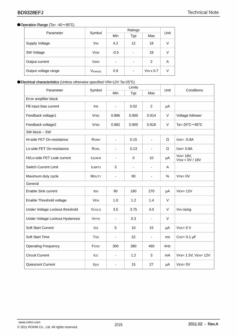
Operation Range (Ta= -40~85)
Parameter Symbol Ratings
Unit Min Typ Max
Supply Voltage VIN 4.2 12 18 V
SW Voltage VSW -0.5 - 18 V
Output current ISW3 - - 2 A
Output voltage range VRANGE 0.9 - VIN x 0.7 V
Electrical characteristics (Unless otherwise specified VIN=12V Ta=25)
Parameter Symbol Limits
Unit Conditions Min Typ Max
Error amplifier block
FB input bias current IFB - 0.02 2 µA
Feedback voltage1 VFB1 0.886 0.900 0.914 V Voltage follower
Feedback voltage2 VFB2 0.882 0.900 0.918 V Ta=-25~85
SW block – SW
Hi-side FET On-resistance RONH - 0.15 - Ω ISW= -0.8A
Lo-side FET On-resistance RONL - 0.13 - Ω ISW= 0.8A
Hi/Lo-side FET Leak current ILEAKN - 0 10 µA VIN= 18V, VSW = 0V / 18V
Switch Current Limit ILIMIT3 3 - - A
Maximum duty cycle MDUTY - 90 - % VFB= 0V
General
Enable Sink current IEN 90 180 270 µA VEN= 12V
Enable Threshold voltage VEN 1.0 1.2 1.4 V
Under Voltage Lockout threshold VUVLO 3.5 3.75 4.0 V VIN rising
Under Voltage Lockout Hysteresis VHYS - 0.3 - V
Soft Start Current ISS 5 10 15 µA VSS= 0 V
Soft Start Time TSS - 22 - ms CSS= 0.1 µF
Operating Frequency FOSC 300 380 460 kHz
Circuit Current ICC - 1.2 3 mA VFB= 1.5V, VEN= 12V
Quiescent Current IQUI - 15 27 µA VEN= 0V

Technical Note
3/15 www.rohm.com 2011.02 - Rev.A
© 2011 ROHM Co., Ltd. All rights reserved.
BD9328EFJ
Block Diagram
Fig.1 Block Diagram Typical Application Circuit
※R_BS protect from VIN-BST short destruction.
Fig.2 Application Circuit
Symbol Maker Part No
Input capacitor C_VC1 TDK C3225JB1E106K 10µF/25V
Output capacitor C_CO1 TDK C3216JB1C106M 10µF/16V
Inductor L TDK SLF10165-100M3R8 10µH/3.8A
-
VREF
TSD
UVLO IBIAS
ERR
Soft Start
SLOPE +
- PWM
VREGOSC 5V
LVS
GND
SW
VIN
BST
SS
VIN
S DRV
LVS
OCP
OUTPUT
12V
+ +
LOGIC R
COMP
FB
EN
C_CO1
R_PC 7.5kΩ
R_UP
C_B
S
0.1μ
F
10µHC_VC1 10μF
C_PC 3300pF R_DW
10kΩ
27kΩ
20μF
C_SS 0.1μF
L
SS
EN
CO
MP
FB
BS
T
VIN
GN
D
SW
Thermal Pad (to be shorted to GND)
VIN 12V VOUT 3.3V
R_B
S
22Ω

Technical Note
4/15 www.rohm.com 2011.02 - Rev.A
© 2011 ROHM Co., Ltd. All rights reserved.
BD9328EFJ
Block Operation ・VREG
A block to generate constant-voltage for DC/DC boosting.
・VREF A block that generates internal reference voltage of 5.1 V (Typ.).
・TSD/UVLO TSD (Thermal shutdown)/UVLO (Under Voltage Lockout) protection block. The TSD circuit shuts down IC at high temperature. The UVLO circuit shuts down the IC when the VCC is Low Voltage.
・Error amp block (ERR) This is the circuit to compare the reference voltage and the feedback voltage of output voltage. The COMP pin voltage resulting from this comparison determines the switching duty. At the time of startup, since the soft start is operated by the SS pin voltage, the COMP pin voltage is limited to the SS pin voltage.
・Oscillator block (OSC) This block generates the oscillating frequency.
・SLOPE block This block generates the triangular waveform from the clock created by OSC. Generated triangular waveform is sent to the PWM comparator.
・PWM block The COMP pin voltage output by the error amp is compared to the SLOPE block's triangular waveform to determine the switching duty. Since the switching duty is limited by the maximum duty ratio which is determined internally, it does not become 100%.
・DRV block A DC/DC driver block. A signal from the PWM is input to drive the power FETs.
・Soft start circuit Since the output voltage rises gradually while restricting the current at the time of startup, it is possible to prevent the output voltage overshoot or the rush current.
Technical Note
5/15 www.rohm.com 2011.02 - Rev.A
© 2011 ROHM Co., Ltd. All rights reserved.
BD9328EFJ
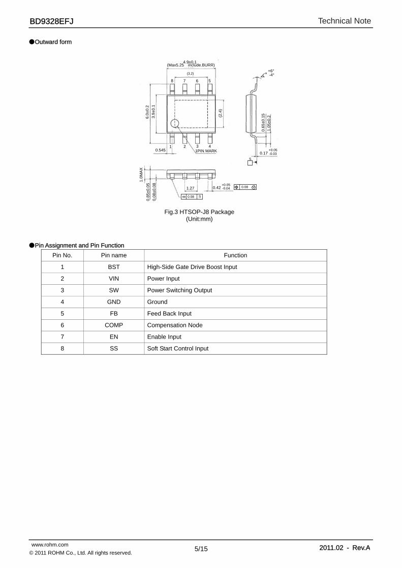
Outward form Pin Assignment and Pin Function
Pin No. Pin name Function
1 BST High-Side Gate Drive Boost Input
2 VIN Power Input
3 SW Power Switching Output
4 GND Ground
5 FB Feed Back Input
6 COMP Compensation Node
7 EN Enable Input
8 SS Soft Start Control Input
Fig.3 HTSOP-J8 Package (Unit:mm)
+0.05 -0.03
4.9±0.1 (Max5.25 include.BURR)
(3.2)
(2.4
)
6.0
±0.2
3.9
±0.1
0.545 1PIN MARK
8 7 6 5
4 3 2 1
1.0
5±0
.2
0.17
1.27 0.42 -0.04
+0.05
0.8
5±0
.05
1.0
MA
X
-4° +6°
S
0.08
0.08
S
+0.05 -0.03
0.6
5±0
.15
0.0
8±0
.08
M

Technical Note
6/15 www.rohm.com 2011.02 - Rev.A
© 2011 ROHM Co., Ltd. All rights reserved.
BD9328EFJ
Typical Performance Characteristics (Unless otherwise specified, VIN= 12V Ta = 25)
1
10
100
1000
0.01 0.1 1
Css[uF]
Soft
sta
rt t
ime[m
s]
Fig.12 Soft Start Time
50
55
60
65
70
75
80
85
90
95
0 500 1000 1500 2000 2500 3000
Io[mA]
Eff
icie
ncy[
%]
Fig.10 STEP Down Efficiency (VIN= 12V VOUT= 3.3V L=10µH)
Fig.9 Operating Frequency
340
345
350
355
360
365
370
-40 -20 0 20 40 60 80
TEMP (°C)
FO
SC
(kH
z)
Fig.6 Input Bias Current
-0.01
-0.005
0
0.005
0.01
0 0.4 0.8 1.2 1.6 2 2.4
VFB (V)
IFB
(uA
)
0
4
8
12
16
20
24
28
32
4 6 8 10 12 14 16 18
VIN (V)
ICC
(uA
)
Fig.5 Stand by current (IC not active)
0.4
0.6
0.8
1
1.2
1.4
1.6
3 6 9 12 15 18
VIN (V)
ICC
(m
A)
Fig.4 Circuit Current (No switching)
0.88
0.89
0.90
0.91
0.92
-40 -20 0 20 40 60 80
TEMP[]
Fee
dbac
k V
olta
ge[V
]
Fig.7 Feedback voltage
0.1
0.14
0.18
0.22
0.26
-40 -20 0 20 40 60 80
TEMP [°C]
RO
N [Ω
]
Fig.8 Hi,Low-Side On-resistance
SS
Iout
SW
Vout
Fig.11 OverCurrent Protection
Technical Note
7/15 www.rohm.com 2011.02 - Rev.A
© 2011 ROHM Co., Ltd. All rights reserved.
BD9328EFJ
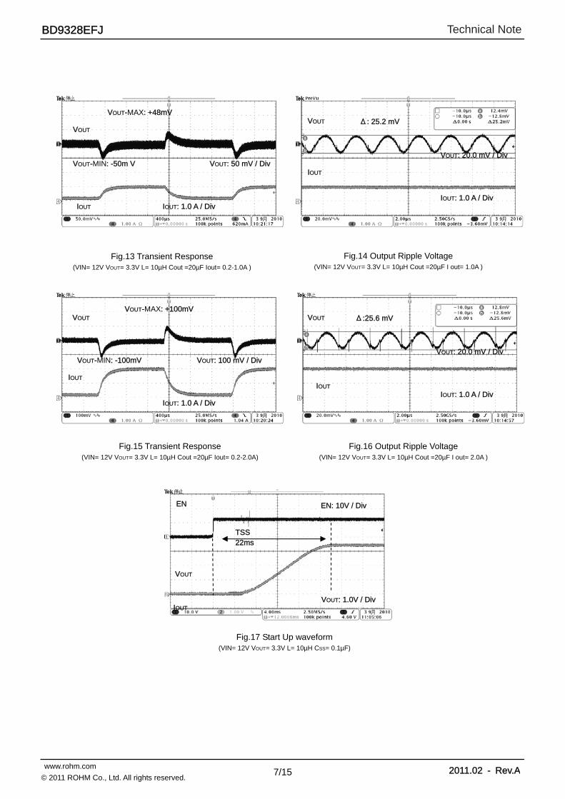
Fig.13 Transient Response (VIN= 12V VOUT= 3.3V L= 10µH Cout =20µF Iout= 0.2-1.0A )
Fig.17 Start Up waveform (VIN= 12V VOUT= 3.3V L= 10µH CSS= 0.1µF)
Fig.15 Transient Response (VIN= 12V VOUT= 3.3V L= 10µH Cout =20µF Iout= 0.2-2.0A)
Fig.16 Output Ripple Voltage (VIN= 12V VOUT= 3.3V L= 10µH Cout =20µF I out= 2.0A )
VOUT
IOUT
VOUT
VOUT
VOUT
VOUT
IOUT
IOUT
IOUT
EN
VOUT: 50 mV / Div
VOUT: 100 mV / Div
IOUT: 1.0 A / Div
IOUT: 1.0 A / Div
VOUT: 20.0 mV / Div
IOUT: 1.0 A / Div
IOUT
Δ:25.6 mV
Δ: 25.2 mV
VOUT-MAX: +100mV
VOUT-MIN: -100mV
VOUT-MAX: +48mV
VOUT-MIN: -50m V
VOUT: 1.0V / Div
EN: 10V / Div
VOUT: 20.0 mV / Div
IOUT: 1.0 A / Div
Fig.14 Output Ripple Voltage (VIN= 12V VOUT= 3.3V L= 10µH Cout =20µF I out= 1.0A )
TSS 22ms

Technical Note
8/15 www.rohm.com 2011.02 - Rev.A
© 2011 ROHM Co., Ltd. All rights reserved.
BD9328EFJ
Selecting Application Components
(1) Output LC filter constant selection (Buck Converter) The Output LC filter is required to supply constant current to the output load. A larger value inductance at this filter results in less inductor ripple current(∆IL) and less output ripple voltage. However, the larger value inductors tend to have less fast load transient-response, a larger physical size, a lower saturation current and higher series resistance. A smaller value inductance has almost opposite characteristics above. So Choosing the Inductor ripple current(∆IL) between 20 to 40% of the averaged inductor current (equivalent to the output load current) is a good compromise.
Fig.18 Fig.19
Setting ∆IL = 30% x Averaged Inductor current (2A) = 0.6 [A]
L = VOUT (VIN - VOUT) x 1
= 10µ [H] VIN x FOSC x ∆IL
Where VIN= 12V, VOUT= 3.3V, FOSC= 380 kHz, ; FOSC is a switching frequency
Also the inductor should have the higher saturation current than IOUTMAX + ∆IL / 2. The output capacitor COUT affects the output ripple-voltage. Choose the large capacitor to achieve the small ripple-voltage enough to meet the application requirement. Output ripple voltage ∆VRPL is calculated by the following equation.
Where RESR is a parasitic series resistance in output capacitor.
Setting COUT = 20µF, RESR = 10mΩ ∆VRPL = 0.6 x (10m + 1 / (8 x 20µ x 380k)) = 15.8mV
∆VRPL = ∆IL ( RESR + 1
) [V] 8x COUT x FOSC
VOUT
L
VIN
COUT
IL
t
IOUTMAX + IL /2 should not reach the rated value level
ILR
Inductor averaged current

Technical Note
9/15 www.rohm.com 2011.02 - Rev.A
© 2011 ROHM Co., Ltd. All rights reserved.
BD9328EFJ
PHASE MARGIN -180°
-90°
-180
-90
0
0
A (a)
GBW(b)
F
F
Gain [dB]
PHASE FCRS
(2) Loop Compensation
Choosing compensation capacitor CCMP and resistor RCMP The current-mode buck converter has 2-poles and 1-zero system. Choosing the compensation resistor and capacitor is important for a good load-transient response and good stability. The example of DC/DC converter application bode plot is shown below. The compensation resistor RCMP will decides the cross over frequency FCRS (the frequency that the total DC-DC loop-gain falls to 0dB). Setting the higher cross over frequency achieves good response speed, however less stability. While setting the lower cross over frequency shows good stability but worse response speed. The 1/10 of switching frequency for the cross over frequency shows a good performance at most applications. ( i ) Choosing phase compensation resistor RCMP
The compensation resistor RCMP can be on following formula.
RCMP = 2πx VOUT x FCRS x COUT
[Ω] VFB x GMP x GMA
Where VOUT; Output voltage, FCRS; Cross over frequency, COUT; Output Capacitor, VFB; internal feedback voltage (0.9V(TYP)), GMP ; Current Sense Gain (7.8A/V(TYP)) , GMA ; Error Amplifier Trans-conductance (300µA/V(TYP))
Setting VOUT= 3.3V, FCRS= 38kHz, COUT= 20µF;
RCMP = 2πx 3.3 x 38k x 20u
= 7.48k ~= 7.5k [Ω] 0.9 x 7.8 x 300u
( ii ) Choosing phase compensation capacitor CCMP
For the stability of DC/DC converter, canceling the phase delay that derives from output capacitor COUT and resistive load ROUT by inserting the phase advance. The phase advance can be added by the zero on compensation resistor RCMP and capacitor CCMP. Making Fz= FCRS / 6 gives a first-order estimate of CCMP.
Compensation Capacitor CCMP= 1
[F] 2π x RCMP x Fz
Setting Fz= FCRS/6 = 6.3kHz;
Compensation Capacitor CCMP= 1
= 3.54n ~= 3.3n [F] 2π x 7.5k x 6.3k
( iii ) The condition of the loop compensation stability
The stability of DC/DC converter is important. To secure the operating stability, please check the loop compensation has the enough phase-margin. For the condition of loop compensation stability, the phase-delay must be less than 150 degree where Gain is 0 dB. Feed forward capacitor CRUP boosts phase margin over a limited frequency range and is sometimes used to improve loop response. CRUP will be more effective if RUP >> RUP||RDW
Fig.20 Fig.21
-
+
VOUT
RUP
CCMP
COMP
RCMP
FB
RDW
0.9V
CRUP
Technical Note
10/15 www.rohm.com 2011.02 - Rev.A
© 2011 ROHM Co., Ltd. All rights reserved.
BD9328EFJ
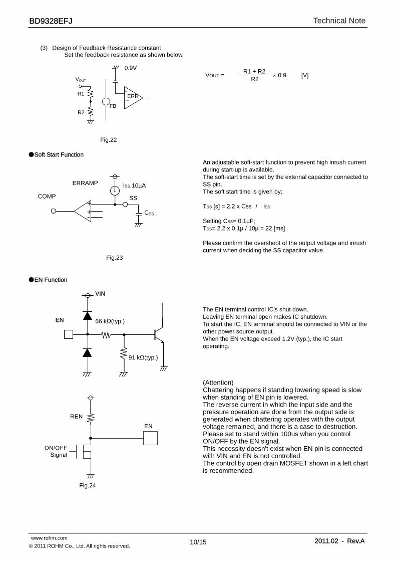
(3) Design of Feedback Resistance constant
Set the feedback resistance as shown below.
VOUT = R1 + R2
0.9 [V] R2
Fig.22 Soft Start Function
An adjustable soft-start function to prevent high inrush current during start-up is available. The soft-start time is set by the external capacitor connected to SS pin. The soft start time is given by; TSS [s] = 2.2 x Css / ISS Setting CSS= 0.1µF; TSS= 2.2 x 0.1µ / 10µ = 22 [ms] Please confirm the overshoot of the output voltage and inrush current when deciding the SS capacitor value.
Fig.23 EN Function
The EN terminal control IC’s shut down. Leaving EN terminal open makes IC shutdown. To start the IC, EN terminal should be connected to VIN or the other power source output. When the EN voltage exceed 1.2V (typ.), the IC start operating. (Attention) Chattering happens if standing lowering speed is slow when standing of EN pin is lowered. The reverse current in which the input side and the pressure operation are done from the output side is generated when chattering operates with the output voltage remained, and there is a case to destruction. Please set to stand within 100us when you control ON/OFF by the EN signal. This necessity doesn't exist when EN pin is connected with VIN and EN is not controlled. The control by open drain MOSFET shown in a left chart is recommended.
Fig.24
VIN
EN
66 kΩ(typ.)
91 kΩ(typ.)
+
-
VOUT
R1
R2
ERR
0.9V
FB
REN
ON/OFFSignal
EN
CSS
SS + +-
COMP
ISS 10µA ERRAMP
↓

Technical Note
11/15 www.rohm.com 2011.02 - Rev.A
© 2011 ROHM Co., Ltd. All rights reserved.
BD9328EFJ
CIN FET COUT
L VOUT
VIN
Layout Pattern Consideration Two high pulsing current flowing loops exist in the buck regulator system. The first loop, when FET is ON, starts from the input capacitors, to the VIN terminal, to the SW terminal, to the inductor, to the output capacitors, and then returns to the input capacitor through GND. The second loop, when FET is OFF, starts from the low FET, to the inductor, to the output capacitor, and then returns to the low FET through GND. To reduce the noise and improve the efficiency, please minimize these two loop area. Especially input capacitor, output capacitor and low FET should be connected to GND plain. PCB Layout may affect the thermal performance, noise and efficiency greatly. So please take extra care when designing PCB Layout patterns. ・The thermal Pad on the back side of IC has the great thermal conduction to the chip. So using the GND plain as broad and
wide as possible can help thermal dissipation. And a lot of thermal via for helping the spread of heat to the different layer is also effective.
・The input capacitors should be connected as close as possible to the VIN terminal. ・Keep sensitive signal traces such as trace connected FB and COMP away from SW pin. ・The inductor and the output capacitors should be placed close to SW pin as much as possible.
COMP
BST
VIN
SW
FB
SS
EN
GND
COUTL
VOUT
CIN
Fig.25 Current loop in Buck regulator system
Fig.26 The example of PCB layout pattern

Technical Note
12/15 www.rohm.com 2011.02 - Rev.A
© 2011 ROHM Co., Ltd. All rights reserved.
BD9328EFJ
I/O Equivalent Circuit Diagram
1.BST 3.SW 5.FB
6.COMP 7.EN 8.SS
Power Dissipation
HTSOP-J8 Package On 70 70 1.6 mm glass epoxy PCB (1) 1-layer board (Backside copper foil area 0 mm 0 mm) (2) 2-layer board (Backside copper foil area 15 mm 15 mm) (3) 2-layer board (Backside copper foil area 70 mm 70 mm) (4) 4-layer board (Backside copper foil area 70 mm 70 mm)
150
0
50 75 100 125
2000
4000
1000
3000
25
PO
WE
R D
ISS
IPA
TIO
N: P
D [m
W]
AMBIENT TEMPERATURE: Ta [°C]
(1)820mW
(2)1100mW
(3)2110mW
(4)3760mW
0
VIN VIN
SW
REG
VIN VINEF
VIN VIN
VIN

Technical Note
13/15 www.rohm.com 2011.02 - Rev.A
© 2011 ROHM Co., Ltd. All rights reserved.
BD9328EFJ
(Pin A)
GND
N
P
N N
P+ P+
Resistor
Parasitic elements P
~
~
~
~
Parasitic elements
(Pin B)
GND
C B
E
Parasitic elements
GND
(Pin A)
~
~
GND
N
P
N N
P+ P+
Parasitic elements
P substrate
(Pin B) C
B
E
Transistor (NPN)
~
~
NGND
Notes for use 1) Absolute maximum ratings
Use of the IC in excess of absolute maximum ratings such as the applied voltage or operating temperature range may result in IC damage. Assumptions should not be made regarding the state of the IC (short mode or open mode) when such damage is suffered. A physical safety measure such as a fuse should be implemented when use of the IC in a special mode where the absolute maximum ratings may be exceeded is anticipated.
2) GND potential Ensure a minimum GND pin potential in all operating conditions.
3) Setting of heat Use a thermal design that allows for a sufficient margin in light of the power dissipation (Pd) in actual operating conditions.
4) Pin short and mistake fitting Use caution when orienting and positioning the IC for mounting on printed circuit boards. Improper mounting may result in damage to the IC. Shorts between output pins or between output pins and the power supply and GND pins caused by the presence of a foreign object may result in damage to the IC.
5) Actions in strong magnetic field Use caution when using the IC in the presence of a strong magnetic field as doing so may cause the IC to malfunction.
6) Testing on application boards When testing the IC on an application board, connecting a capacitor to a pin with low impedance subjects the IC to stress. Always discharge capacitors after each process or step. Ground the IC during assembly steps as an antistatic measure, and use similar caution when transporting or storing the IC. Always turn the IC's power supply off before connecting it to or removing it from a jig or fixture during the inspection process.
7) Ground wiring patterns When using both small signal and large current GND patterns, it is recommended to isolate the two ground patterns, placing a single ground point at the application's reference point so that the pattern wiring resistance and voltage variations caused by large currents do not cause variations in the small signal ground voltage. Be careful not to change the GND wiring patterns of any external components.
8) Regarding input pin of the IC This monolithic IC contains P+ isolation and P substrate layers between adjacent elements in order to keep them isolated. P/N junctions are formed at the intersection of these P layers with the N layers of other elements to create a variety of parasitic elements. For example, when the resistors and transistors are connected to the pins as shown in Fig.27 , a parasitic diode or a transistor operates by inverting the pin voltage and GND voltage. The formation of parasitic elements as a result of the relationships of the potentials of different pins is an inevitable result of the IC's architecture. The operation of parasitic elements can cause interference with circuit operation as well as IC malfunction and damage. For these reasons, it is necessary to use caution so that the IC is not used in a way that will trigger the operation of parasitic elements such as by the application of voltages lower than the GND (P substrate) voltage to input and output pins.
Fig.27 Example of a Simple Monolithic IC Architecture

Technical Note
14/15 www.rohm.com 2011.02 - Rev.A
© 2011 ROHM Co., Ltd. All rights reserved.
BD9328EFJ
9) Overcurrent protection circuits
An overcurrent protection circuit designed according to the output current is incorporated for the prevention of IC damage that may result in the event of load shorting. This protection circuit is effective in preventing damage due to sudden and unexpected accidents. However, the IC should not be used in applications characterized by the continuous operation or transitioning of the protection circuits. At the time of thermal designing, keep in mind that the current capacity has negative characteristics to temperatures.
10) Thermal shutdown circuit (TSD) This IC incorporates a built-in TSD circuit for the protection from thermal destruction. The IC should be used within the specified power dissipation range. However, in the event that the IC continues to be operated in excess of its power dissipation limits, the attendant rise in the chip's junction temperature Tj will trigger the TSD circuit to turn off all output power elements. Operation of the TSD circuit presumes that the IC's absolute maximum ratings have been exceeded. Application designs should never make use of the TSD circuit.
11) Testing on application boards At the time of inspection of the installation boards, when the capacitor is connected to the pin with low impedance, be sure to discharge electricity per process because it may load stresses to the IC. Always turn the IC's power supply off before connecting it to or removing it from a jig or fixture during the inspection process. Ground the IC during assembly steps as an antistatic measure, and use similar caution when transporting or storing the IC.
12) EN control speed Chattering happens if standing lowering speed is slow when standing of EN pin is lowered. The reverse current in which the input side and the pressure operation are done from the output side is generated when chattering operates with the output voltage remained, and there is a case to destruction. Please set to stand within 100us when you control ON/OFF by the EN signal.

Technical Note
15/15 www.rohm.com 2011.02 - Rev.A
© 2011 ROHM Co., Ltd. All rights reserved.
BD9328EFJ
Ordering part number
B D 9 3 2 8 E F J - E 2
Part No. Part No.
Package EFJ: HTSOP-J8
Packaging and forming specification
E2: Embossed tape and reel
(Unit : mm)
HTSOP-J8
0.08 S
0.08 M
S
1.0M
AX
0.85
±0.0
5
1.27
0.08
±0.0
8 0.42+0.05-0.04
1.05
±0.2
0.65
±0.1
5
4°+6°−4°
0.17+0.05-0.03
2 3 4
568
(MAX 5.25 include BURR)
7
1
0.545
(3.2)
4.9±0.1
6.0±
0.2
(2.4
)
3.9±
0.1
1PIN MARK
∗ Order quantity needs to be multiple of the minimum quantity.
<Tape and Reel information>
Embossed carrier tapeTape
Quantity
Direction of feed The direction is the 1pin of product is at the upper left when you hold
reel on the left hand and you pull out the tape on the right hand
2500pcs
E2
( )
Direction of feed
Reel1pin

DatasheetDatasheet
Notice - GE Rev.002© 2014 ROHM Co., Ltd. All rights reserved.
Notice Precaution on using ROHM Products
1. Our Products are designed and manufactured for application in ordinary electronic equipments (such as AV equipment, OA equipment, telecommunication equipment, home electronic appliances, amusement equipment, etc.). If you intend to use our Products in devices requiring extremely high reliability (such as medical equipment (Note 1), transport equipment, traffic equipment, aircraft/spacecraft, nuclear power controllers, fuel controllers, car equipment including car accessories, safety devices, etc.) and whose malfunction or failure may cause loss of human life, bodily injury or serious damage to property (“Specific Applications”), please consult with the ROHM sales representative in advance. Unless otherwise agreed in writing by ROHM in advance, ROHM shall not be in any way responsible or liable for any damages, expenses or losses incurred by you or third parties arising from the use of any ROHM’s Products for Specific Applications.
(Note1) Medical Equipment Classification of the Specific Applications JAPAN USA EU CHINA
CLASSⅢ CLASSⅢ
CLASSⅡb CLASSⅢ
CLASSⅣ CLASSⅢ
2. ROHM designs and manufactures its Products subject to strict quality control system. However, semiconductor
products can fail or malfunction at a certain rate. Please be sure to implement, at your own responsibilities, adequate safety measures including but not limited to fail-safe design against the physical injury, damage to any property, which a failure or malfunction of our Products may cause. The following are examples of safety measures:
[a] Installation of protection circuits or other protective devices to improve system safety [b] Installation of redundant circuits to reduce the impact of single or multiple circuit failure
3. Our Products are designed and manufactured for use under standard conditions and not under any special or extraordinary environments or conditions, as exemplified below. Accordingly, ROHM shall not be in any way responsible or liable for any damages, expenses or losses arising from the use of any ROHM’s Products under any special or extraordinary environments or conditions. If you intend to use our Products under any special or extraordinary environments or conditions (as exemplified below), your independent verification and confirmation of product performance, reliability, etc, prior to use, must be necessary:
[a] Use of our Products in any types of liquid, including water, oils, chemicals, and organic solvents [b] Use of our Products outdoors or in places where the Products are exposed to direct sunlight or dust [c] Use of our Products in places where the Products are exposed to sea wind or corrosive gases, including Cl2,
H2S, NH3, SO2, and NO2
[d] Use of our Products in places where the Products are exposed to static electricity or electromagnetic waves [e] Use of our Products in proximity to heat-producing components, plastic cords, or other flammable items [f] Sealing or coating our Products with resin or other coating materials [g] Use of our Products without cleaning residue of flux (even if you use no-clean type fluxes, cleaning residue of
flux is recommended); or Washing our Products by using water or water-soluble cleaning agents for cleaning residue after soldering
[h] Use of the Products in places subject to dew condensation
4. The Products are not subject to radiation-proof design. 5. Please verify and confirm characteristics of the final or mounted products in using the Products. 6. In particular, if a transient load (a large amount of load applied in a short period of time, such as pulse. is applied,
confirmation of performance characteristics after on-board mounting is strongly recommended. Avoid applying power exceeding normal rated power; exceeding the power rating under steady-state loading condition may negatively affect product performance and reliability.
7. De-rate Power Dissipation (Pd) depending on Ambient temperature (Ta). When used in sealed area, confirm the actual
ambient temperature. 8. Confirm that operation temperature is within the specified range described in the product specification. 9. ROHM shall not be in any way responsible or liable for failure induced under deviant condition from what is defined in
this document.
Precaution for Mounting / Circuit board design 1. When a highly active halogenous (chlorine, bromine, etc.) flux is used, the residue of flux may negatively affect product
performance and reliability. 2. In principle, the reflow soldering method must be used; if flow soldering method is preferred, please consult with the
ROHM representative in advance. For details, please refer to ROHM Mounting specification

DatasheetDatasheet
Notice - GE Rev.002© 2014 ROHM Co., Ltd. All rights reserved.
Precautions Regarding Application Examples and External Circuits 1. If change is made to the constant of an external circuit, please allow a sufficient margin considering variations of the
characteristics of the Products and external components, including transient characteristics, as well as static characteristics.
2. You agree that application notes, reference designs, and associated data and information contained in this document
are presented only as guidance for Products use. Therefore, in case you use such information, you are solely responsible for it and you must exercise your own independent verification and judgment in the use of such information contained in this document. ROHM shall not be in any way responsible or liable for any damages, expenses or losses incurred by you or third parties arising from the use of such information.
Precaution for Electrostatic
This Product is electrostatic sensitive product, which may be damaged due to electrostatic discharge. Please take proper caution in your manufacturing process and storage so that voltage exceeding the Products maximum rating will not be applied to Products. Please take special care under dry condition (e.g. Grounding of human body / equipment / solder iron, isolation from charged objects, setting of Ionizer, friction prevention and temperature / humidity control).
Precaution for Storage / Transportation 1. Product performance and soldered connections may deteriorate if the Products are stored in the places where:
[a] the Products are exposed to sea winds or corrosive gases, including Cl2, H2S, NH3, SO2, and NO2 [b] the temperature or humidity exceeds those recommended by ROHM [c] the Products are exposed to direct sunshine or condensation [d] the Products are exposed to high Electrostatic
2. Even under ROHM recommended storage condition, solderability of products out of recommended storage time period may be degraded. It is strongly recommended to confirm solderability before using Products of which storage time is exceeding the recommended storage time period.
3. Store / transport cartons in the correct direction, which is indicated on a carton with a symbol. Otherwise bent leads
may occur due to excessive stress applied when dropping of a carton. 4. Use Products within the specified time after opening a humidity barrier bag. Baking is required before using Products of
which storage time is exceeding the recommended storage time period.
Precaution for Product Label QR code printed on ROHM Products label is for ROHM’s internal use only.
Precaution for Disposition When disposing Products please dispose them properly using an authorized industry waste company.
Precaution for Foreign Exchange and Foreign Trade act Since our Products might fall under controlled goods prescribed by the applicable foreign exchange and foreign trade act, please consult with ROHM representative in case of export.
Precaution Regarding Intellectual Property Rights 1. All information and data including but not limited to application example contained in this document is for reference
only. ROHM does not warrant that foregoing information or data will not infringe any intellectual property rights or any other rights of any third party regarding such information or data. ROHM shall not be in any way responsible or liable for infringement of any intellectual property rights or other damages arising from use of such information or data.:
2. No license, expressly or implied, is granted hereby under any intellectual property rights or other rights of ROHM or any
third parties with respect to the information contained in this document.
Other Precaution 1. This document may not be reprinted or reproduced, in whole or in part, without prior written consent of ROHM. 2. The Products may not be disassembled, converted, modified, reproduced or otherwise changed without prior written
consent of ROHM. 3. In no event shall you use in any way whatsoever the Products and the related technical information contained in the
Products or this document for any military purposes, including but not limited to, the development of mass-destruction weapons.
4. The proper names of companies or products described in this document are trademarks or registered trademarks of
ROHM, its affiliated companies or third parties.

DatasheetDatasheet
Notice – WE Rev.001© 2014 ROHM Co., Ltd. All rights reserved.
General Precaution 1. Before you use our Pro ducts, you are requested to care fully read this document and fully understand its contents.
ROHM shall n ot be in an y way responsible or liabl e for fa ilure, malfunction or acci dent arising from the use of a ny ROHM’s Products against warning, caution or note contained in this document.
2. All information contained in this docume nt is current as of the issuing date and subj ect to change without any prior
notice. Before purchasing or using ROHM’s Products, please confirm the la test information with a ROHM sale s representative.
3. The information contained in this doc ument is provi ded on an “as is” basis and ROHM does not warrant that all
information contained in this document is accurate an d/or error-free. ROHM shall not be in an y way responsible or liable for any damages, expenses or losses incurred by you or third parties resulting from inaccuracy or errors of or concerning such information.