Embed Size (px)
Citation preview
This is information on a product in full production.
May 2013 DocID023416 Rev 4 1/42
1
L9959S L9959T
Single and dual PMOS high-side H-bridge
Datasheet - production data
Features
Full path RDSON less than 540 m
Continuous load current > 3 A
Operating battery supply voltage 5 V to 28 V
Operating VDD supply voltage 4.5 V to 5.5 V
All ECU internal pins can withstand up to 18 V
Output switching frequency up to 11 kHz
Monitoring of VDD supply voltage
SPI programmable output current limitation from 5 A to 8.6 A (in 3 steps)
Over temperature and short circuit protection
Full diagnosis capability
Fast switch-off open-drain input/output
Current-monitoring with current feedback output signal CF
SPI-interface for configuration and diagnosis
Error history in second diagnosis register
Two independent enable pins: "/ABE" and "DIS"
Control of power stages by SPI or two input signals, PWM and DIR (configurable via SPI)
Logic levels 5 V compatible
Conformity to improved EMC requirements due to smart H-bridge switching
Description
L9959S and L9959T are a single and dual integrated H-bridges for resistive and inductive loads featuring output current direction and supervising functions.
The PowerSSO24 houses one full H-Bridge, while the PowerSSO36 houses two H-Bridges that can work in parallel, through independent input driving commands.
Target application ranges from throttle control actuators to exhaust gas recirculation control valves in automotive domain to a more general use to drive DC and Stepper motors.
PowerSSO24 PowerSSO36
Table 1. Device summary
Order code Package Packing
L9959S-TR PowerSSO24 Tape & Reel
L9959T-TR PowerSSO36 Tape & Reel
www.st.com
Contents L9959S, L9959T
2/42 DocID023416 Rev 4
Contents
1 Block diagram . . . . . . . . . . . . . . . . . . . . . . . . . . . . . . . . . . . . . . . . . . . . . . 6
2 Pins description . . . . . . . . . . . . . . . . . . . . . . . . . . . . . . . . . . . . . . . . . . . . 7
2.1 Pin definitions and functions . . . . . . . . . . . . . . . . . . . . . . . . . . . . . . . . . . . . 8
3 Electrical specifications . . . . . . . . . . . . . . . . . . . . . . . . . . . . . . . . . . . . . 11
3.1 Absolute maximum ratings . . . . . . . . . . . . . . . . . . . . . . . . . . . . . . . . . . . . .11
3.2 ESD protection . . . . . . . . . . . . . . . . . . . . . . . . . . . . . . . . . . . . . . . . . . . . . .11
3.3 Thermal data . . . . . . . . . . . . . . . . . . . . . . . . . . . . . . . . . . . . . . . . . . . . . . 12
3.4 Electrical characteristics . . . . . . . . . . . . . . . . . . . . . . . . . . . . . . . . . . . . . . 12
3.5 Outputs OUT1 and OUT2 . . . . . . . . . . . . . . . . . . . . . . . . . . . . . . . . . . . . . 14
3.6 Temperature dependent current reduction . . . . . . . . . . . . . . . . . . . . . . . . 18
3.7 Free-wheeling diodes . . . . . . . . . . . . . . . . . . . . . . . . . . . . . . . . . . . . . . . . 18
3.8 SPI / logic electrical characteristics . . . . . . . . . . . . . . . . . . . . . . . . . . . . . 19
4 Application information . . . . . . . . . . . . . . . . . . . . . . . . . . . . . . . . . . . . . 21
4.1 Power stage switching behavior . . . . . . . . . . . . . . . . . . . . . . . . . . . . . . . . 21
4.1.1 PWM mode (same current direction) . . . . . . . . . . . . . . . . . . . . . . . . . . . 21
4.2 Protection and monitoring . . . . . . . . . . . . . . . . . . . . . . . . . . . . . . . . . . . . 23
4.2.1 Current feedback . . . . . . . . . . . . . . . . . . . . . . . . . . . . . . . . . . . . . . . . . . 24
4.2.2 Current limitation . . . . . . . . . . . . . . . . . . . . . . . . . . . . . . . . . . . . . . . . . . 24
4.2.3 Temperature dependent current reduction . . . . . . . . . . . . . . . . . . . . . . . 25
4.2.4 Short to battery (SCB) and short to Ground (SCG) . . . . . . . . . . . . . . . . 25
4.2.5 Short circuit over load (SCL) . . . . . . . . . . . . . . . . . . . . . . . . . . . . . . . . . 26
4.2.6 Open load (OL) . . . . . . . . . . . . . . . . . . . . . . . . . . . . . . . . . . . . . . . . . . . 26
4.3 VS-undervoltage . . . . . . . . . . . . . . . . . . . . . . . . . . . . . . . . . . . . . . . . . . . . 27
4.4 Inverse current at VS . . . . . . . . . . . . . . . . . . . . . . . . . . . . . . . . . . . . . . . . . . . . . . . . . . . . 27
4.5 /ABE pin . . . . . . . . . . . . . . . . . . . . . . . . . . . . . . . . . . . . . . . . . . . . . . . . . . 27
4.6 VDD-monitor . . . . . . . . . . . . . . . . . . . . . . . . . . . . . . . . . . . . . . . . . . . . . . . 27
4.7 VDD-monitor test . . . . . . . . . . . . . . . . . . . . . . . . . . . . . . . . . . . . . . . . . . . 27
4.8 Power-on reset . . . . . . . . . . . . . . . . . . . . . . . . . . . . . . . . . . . . . . . . . . . . . 28
5 SPI functional description . . . . . . . . . . . . . . . . . . . . . . . . . . . . . . . . . . . 29
DocID023416 Rev 4 3/42
L9959S, L9959T Contents
5.1 General description . . . . . . . . . . . . . . . . . . . . . . . . . . . . . . . . . . . . . . . . . 29
5.1.1 SPI select (SS) . . . . . . . . . . . . . . . . . . . . . . . . . . . . . . . . . . . . . . . . . . . 29
5.1.2 Serial data In (SI) . . . . . . . . . . . . . . . . . . . . . . . . . . . . . . . . . . . . . . . . . . 29
5.1.3 Serial clock (SCK) . . . . . . . . . . . . . . . . . . . . . . . . . . . . . . . . . . . . . . . . . 29
5.1.4 Serial out (SO) . . . . . . . . . . . . . . . . . . . . . . . . . . . . . . . . . . . . . . . . . . . . 29
5.1.5 SPI communication flow . . . . . . . . . . . . . . . . . . . . . . . . . . . . . . . . . . . . 29
5.2 SPI-instruction . . . . . . . . . . . . . . . . . . . . . . . . . . . . . . . . . . . . . . . . . . . . . 31
5.3 Device register map . . . . . . . . . . . . . . . . . . . . . . . . . . . . . . . . . . . . . . . . . 31
5.4 SPI - control and status registers . . . . . . . . . . . . . . . . . . . . . . . . . . . . . . . 32
5.4.1 Reset sources . . . . . . . . . . . . . . . . . . . . . . . . . . . . . . . . . . . . . . . . . . . . 37
5.4.2 Configuration registers reset sources . . . . . . . . . . . . . . . . . . . . . . . . . . 37
6 Application circuit . . . . . . . . . . . . . . . . . . . . . . . . . . . . . . . . . . . . . . . . . . 38
7 Package information . . . . . . . . . . . . . . . . . . . . . . . . . . . . . . . . . . . . . . . . 39
8 Revision history . . . . . . . . . . . . . . . . . . . . . . . . . . . . . . . . . . . . . . . . . . . 41
List of tables L9959S, L9959T
4/42 DocID023416 Rev 4
List of tables
Table 1. Device summary . . . . . . . . . . . . . . . . . . . . . . . . . . . . . . . . . . . . . . . . . . . . . . . . . . . . . . . . . . 1Table 2. L9959S pinout. . . . . . . . . . . . . . . . . . . . . . . . . . . . . . . . . . . . . . . . . . . . . . . . . . . . . . . . . . . . 8Table 3. L9959T (Two H-Bridge drivers in one package) pinout . . . . . . . . . . . . . . . . . . . . . . . . . . . . 9Table 4. Absolute maximum ratings . . . . . . . . . . . . . . . . . . . . . . . . . . . . . . . . . . . . . . . . . . . . . . . . . 11Table 5. ESD protection . . . . . . . . . . . . . . . . . . . . . . . . . . . . . . . . . . . . . . . . . . . . . . . . . . . . . . . . . . 11Table 6. Thermal data. . . . . . . . . . . . . . . . . . . . . . . . . . . . . . . . . . . . . . . . . . . . . . . . . . . . . . . . . . . . 12Table 7. Supply . . . . . . . . . . . . . . . . . . . . . . . . . . . . . . . . . . . . . . . . . . . . . . . . . . . . . . . . . . . . . . . . . 12Table 8. Power-on reset . . . . . . . . . . . . . . . . . . . . . . . . . . . . . . . . . . . . . . . . . . . . . . . . . . . . . . . . . . 13Table 9. VDD monitoring . . . . . . . . . . . . . . . . . . . . . . . . . . . . . . . . . . . . . . . . . . . . . . . . . . . . . . . . . . 13Table 10. Undervoltage shutdown . . . . . . . . . . . . . . . . . . . . . . . . . . . . . . . . . . . . . . . . . . . . . . . . . . . 14Table 11. On-resistance (4.5 V < VS < 28 V) . . . . . . . . . . . . . . . . . . . . . . . . . . . . . . . . . . . . . . . . . . . 14Table 12. Power output switching times (8 V < VS < 18 V). . . . . . . . . . . . . . . . . . . . . . . . . . . . . . . . . 14Table 13. Current feedback (CF) . . . . . . . . . . . . . . . . . . . . . . . . . . . . . . . . . . . . . . . . . . . . . . . . . . . . 16Table 14. Current limiting . . . . . . . . . . . . . . . . . . . . . . . . . . . . . . . . . . . . . . . . . . . . . . . . . . . . . . . . . . 17Table 15. Over-current detection (8 V < VS < 18 V) . . . . . . . . . . . . . . . . . . . . . . . . . . . . . . . . . . . . . . 17Table 16. Openload detection. . . . . . . . . . . . . . . . . . . . . . . . . . . . . . . . . . . . . . . . . . . . . . . . . . . . . . . 18Table 17. Retest delay . . . . . . . . . . . . . . . . . . . . . . . . . . . . . . . . . . . . . . . . . . . . . . . . . . . . . . . . . . . . 18Table 18. Temperature dependent current reduction . . . . . . . . . . . . . . . . . . . . . . . . . . . . . . . . . . . . . 18Table 19. Free-wheel diodes . . . . . . . . . . . . . . . . . . . . . . . . . . . . . . . . . . . . . . . . . . . . . . . . . . . . . . . 18Table 20. Inputs: SI, SS, SCK, DIR, DIS and PWM; Output: SO . . . . . . . . . . . . . . . . . . . . . . . . . . . . 19Table 21. Dynamic characteristics . . . . . . . . . . . . . . . . . . . . . . . . . . . . . . . . . . . . . . . . . . . . . . . . . . . 20Table 22. Device states with respect to supply voltage . . . . . . . . . . . . . . . . . . . . . . . . . . . . . . . . . . . 28Table 23. SPI instruction byte . . . . . . . . . . . . . . . . . . . . . . . . . . . . . . . . . . . . . . . . . . . . . . . . . . . . . . . 31Table 24. Check byte . . . . . . . . . . . . . . . . . . . . . . . . . . . . . . . . . . . . . . . . . . . . . . . . . . . . . . . . . . . . . 31Table 25. Command overview . . . . . . . . . . . . . . . . . . . . . . . . . . . . . . . . . . . . . . . . . . . . . . . . . . . . . . 31Table 26. Device identifier (ID) . . . . . . . . . . . . . . . . . . . . . . . . . . . . . . . . . . . . . . . . . . . . . . . . . . . . . . 32Table 27. Revision register (REV) . . . . . . . . . . . . . . . . . . . . . . . . . . . . . . . . . . . . . . . . . . . . . . . . . . . 32Table 28. DIA_REG1 . . . . . . . . . . . . . . . . . . . . . . . . . . . . . . . . . . . . . . . . . . . . . . . . . . . . . . . . . . . . . 32Table 29. Diagnosis bits (DIA_REG1) . . . . . . . . . . . . . . . . . . . . . . . . . . . . . . . . . . . . . . . . . . . . . . . . 33Table 30. Diagnosis register 2 (DIA_REG2) . . . . . . . . . . . . . . . . . . . . . . . . . . . . . . . . . . . . . . . . . . . . 33Table 31. Diagnosis bits (DIA_REG2) . . . . . . . . . . . . . . . . . . . . . . . . . . . . . . . . . . . . . . . . . . . . . . . . 34Table 32. Configuration register (CONFIG_REG) . . . . . . . . . . . . . . . . . . . . . . . . . . . . . . . . . . . . . . . 34Table 33. Current Level (CONFIG_REG) . . . . . . . . . . . . . . . . . . . . . . . . . . . . . . . . . . . . . . . . . . . . . . 35Table 34. Status and configuration register (STATCON_REG) . . . . . . . . . . . . . . . . . . . . . . . . . . . . . 35Table 35. Special register (SPECIAL_REG). . . . . . . . . . . . . . . . . . . . . . . . . . . . . . . . . . . . . . . . . . . . 36Table 36. Document revision history . . . . . . . . . . . . . . . . . . . . . . . . . . . . . . . . . . . . . . . . . . . . . . . . . 41
DocID023416 Rev 4 5/42
L9959S, L9959T List of figures
List of figures
Figure 1. Block diagram . . . . . . . . . . . . . . . . . . . . . . . . . . . . . . . . . . . . . . . . . . . . . . . . . . . . . . . . . . . . 6Figure 2. PSSO24 pin connection (top view) . . . . . . . . . . . . . . . . . . . . . . . . . . . . . . . . . . . . . . . . . . . . 7Figure 3. PSSO36 pin connection (top view) . . . . . . . . . . . . . . . . . . . . . . . . . . . . . . . . . . . . . . . . . . . . 7Figure 4. Output delay times (e.g. low-side output) . . . . . . . . . . . . . . . . . . . . . . . . . . . . . . . . . . . . . . 15Figure 5. Output rise and fall times . . . . . . . . . . . . . . . . . . . . . . . . . . . . . . . . . . . . . . . . . . . . . . . . . . 15Figure 6. Output disable and enable time (/ABE Input) . . . . . . . . . . . . . . . . . . . . . . . . . . . . . . . . . . . 15Figure 7. Output disable and enable time (DIS Input) . . . . . . . . . . . . . . . . . . . . . . . . . . . . . . . . . . . . 16Figure 8. SPI timing information. . . . . . . . . . . . . . . . . . . . . . . . . . . . . . . . . . . . . . . . . . . . . . . . . . . . . 20Figure 9. PWM mode current flow . . . . . . . . . . . . . . . . . . . . . . . . . . . . . . . . . . . . . . . . . . . . . . . . . . . 21Figure 10. PWM mode output voltage . . . . . . . . . . . . . . . . . . . . . . . . . . . . . . . . . . . . . . . . . . . . . . . . . 22Figure 11. DIR-change (current is changing its direction) . . . . . . . . . . . . . . . . . . . . . . . . . . . . . . . . . . 22Figure 12. DIR-change current flow phase 2 . . . . . . . . . . . . . . . . . . . . . . . . . . . . . . . . . . . . . . . . . . . . 22Figure 13. DIR-change output voltage . . . . . . . . . . . . . . . . . . . . . . . . . . . . . . . . . . . . . . . . . . . . . . . . . 23Figure 14. Current feedback and current limiting. . . . . . . . . . . . . . . . . . . . . . . . . . . . . . . . . . . . . . . . . 24Figure 15. Current limitation. . . . . . . . . . . . . . . . . . . . . . . . . . . . . . . . . . . . . . . . . . . . . . . . . . . . . . . . . 25Figure 16. Temperature dependent current reduction . . . . . . . . . . . . . . . . . . . . . . . . . . . . . . . . . . . . . 25Figure 17. Current limiting and short circuit . . . . . . . . . . . . . . . . . . . . . . . . . . . . . . . . . . . . . . . . . . . . . 26Figure 18. Write access . . . . . . . . . . . . . . . . . . . . . . . . . . . . . . . . . . . . . . . . . . . . . . . . . . . . . . . . . . . . 30Figure 19. Read access . . . . . . . . . . . . . . . . . . . . . . . . . . . . . . . . . . . . . . . . . . . . . . . . . . . . . . . . . . . . 30Figure 20. Application circuit . . . . . . . . . . . . . . . . . . . . . . . . . . . . . . . . . . . . . . . . . . . . . . . . . . . . . . . . 38Figure 21. PowerSSO24 mechanical data and package dimensions . . . . . . . . . . . . . . . . . . . . . . . . . 39Figure 22. PowerSSO36 mechanical data and package dimensions . . . . . . . . . . . . . . . . . . . . . . . . . 40
Block diagram L9959S, L9959T
6/42 DocID023416 Rev 4
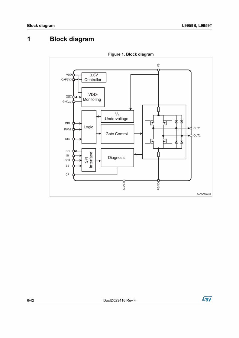
1 Block diagram
Figure 1. Block diagram
DocID023416 Rev 4 7/42
L9959S, L9959T Pins description
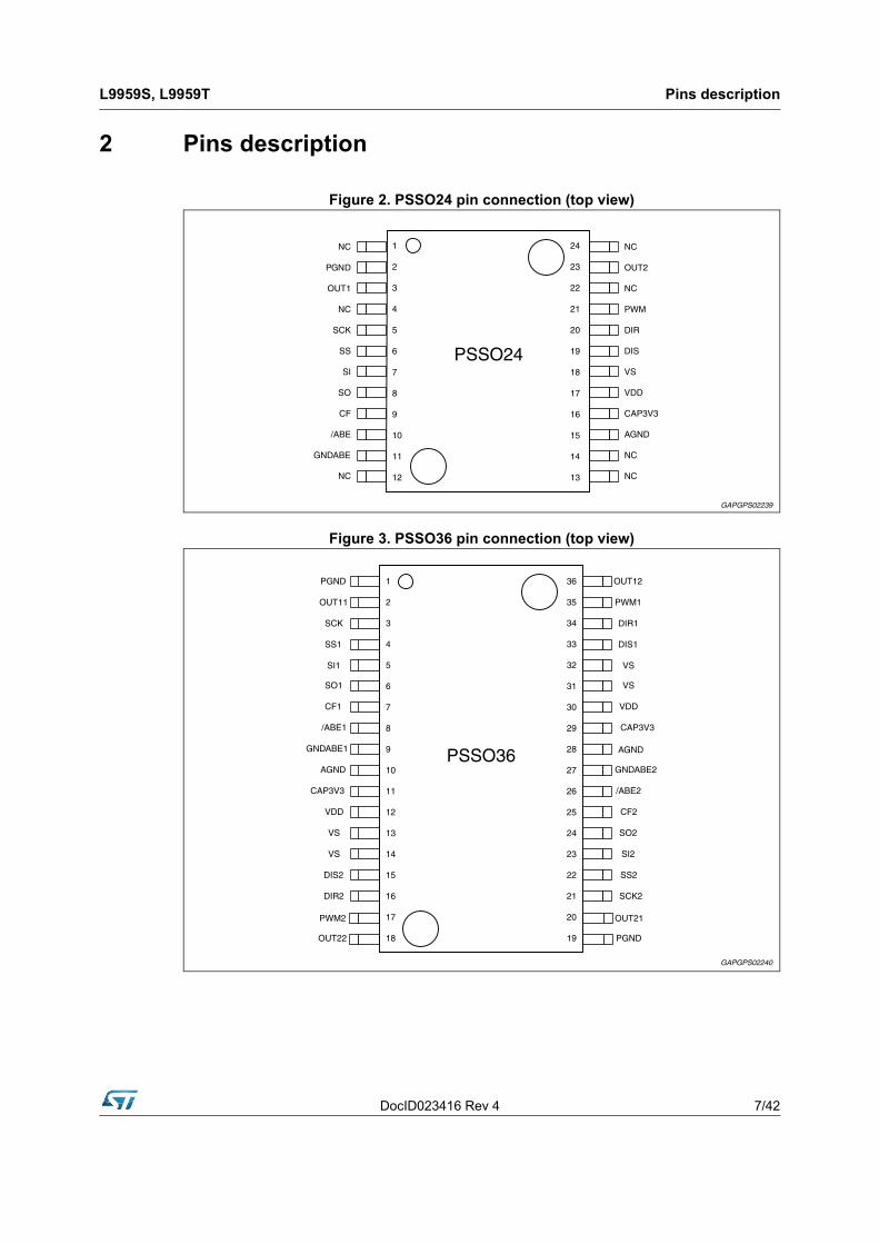
2 Pins description
Figure 2. PSSO24 pin connection (top view)
Figure 3. PSSO36 pin connection (top view)
Pins description L9959S, L9959T
8/42 DocID023416 Rev 4
2.1 Pin definitions and functions
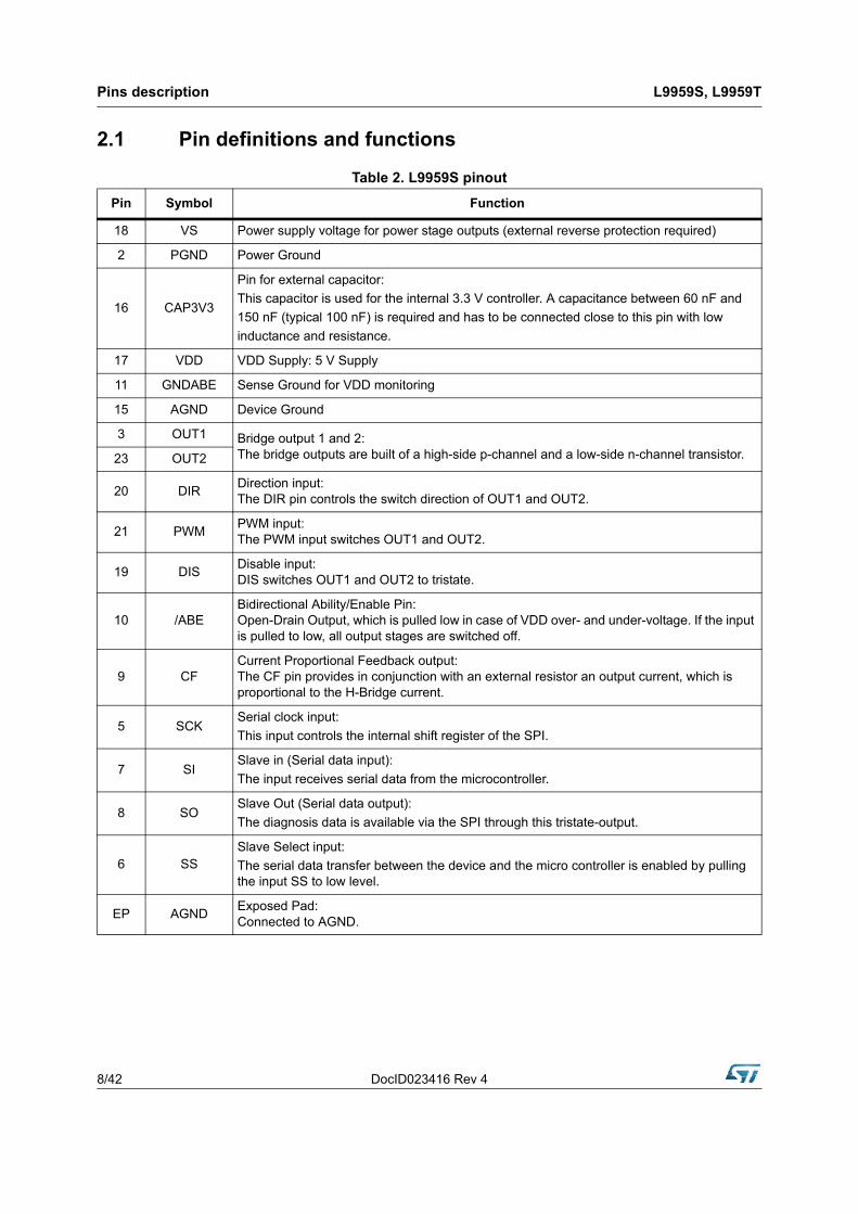
Table 2. L9959S pinout
Pin Symbol Function
18 VS Power supply voltage for power stage outputs (external reverse protection required)
2 PGND Power Ground
16 CAP3V3
Pin for external capacitor:
This capacitor is used for the internal 3.3 V controller. A capacitance between 60 nF and
150 nF (typical 100 nF) is required and has to be connected close to this pin with low
inductance and resistance.
17 VDD VDD Supply: 5 V Supply
11 GNDABE Sense Ground for VDD monitoring
15 AGND Device Ground
3 OUT1 Bridge output 1 and 2: The bridge outputs are built of a high-side p-channel and a low-side n-channel transistor.23 OUT2
20 DIRDirection input: The DIR pin controls the switch direction of OUT1 and OUT2.
21 PWMPWM input:The PWM input switches OUT1 and OUT2.
19 DISDisable input:DIS switches OUT1 and OUT2 to tristate.
10 /ABEBidirectional Ability/Enable Pin: Open-Drain Output, which is pulled low in case of VDD over- and under-voltage. If the input is pulled to low, all output stages are switched off.
9 CFCurrent Proportional Feedback output:The CF pin provides in conjunction with an external resistor an output current, which is proportional to the H-Bridge current.
5 SCKSerial clock input:
This input controls the internal shift register of the SPI.
7 SISlave in (Serial data input):
The input receives serial data from the microcontroller.
8 SOSlave Out (Serial data output):
The diagnosis data is available via the SPI through this tristate-output.
6 SSSlave Select input:
The serial data transfer between the device and the micro controller is enabled by pulling the input SS to low level.
EP AGNDExposed Pad: Connected to AGND.
DocID023416 Rev 4 9/42
L9959S, L9959T Pins description
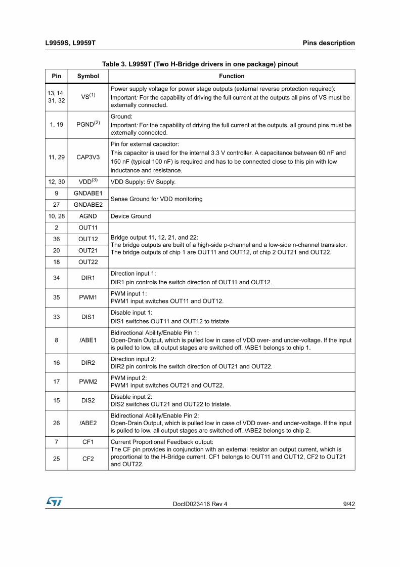
Table 3. L9959T (Two H-Bridge drivers in one package) pinout
Pin Symbol Function
13, 14, 31, 32
VS(1)Power supply voltage for power stage outputs (external reverse protection required):
Important: For the capability of driving the full current at the outputs all pins of VS must be externally connected.
1, 19 PGND(2)Ground:
Important: For the capability of driving the full current at the outputs, all ground pins must be externally connected.
11, 29 CAP3V3
Pin for external capacitor:
This capacitor is used for the internal 3.3 V controller. A capacitance between 60 nF and
150 nF (typical 100 nF) is required and has to be connected close to this pin with low
inductance and resistance.
12, 30 VDD(3) VDD Supply: 5V Supply.
9 GNDABE1Sense Ground for VDD monitoring
27 GNDABE2
10, 28 AGND Device Ground
2 OUT11
Bridge output 11, 12, 21, and 22: The bridge outputs are built of a high-side p-channel and a low-side n-channel transistor. The bridge outputs of chip 1 are OUT11 and OUT12, of chip 2 OUT21 and OUT22.
36 OUT12
20 OUT21
18 OUT22
34 DIR1Direction input 1:
DIR1 pin controls the switch direction of OUT11 and OUT12.
35 PWM1PWM input 1:PWM1 input switches OUT11 and OUT12.
33 DIS1Disable input 1:
DIS1 switches OUT11 and OUT12 to tristate
8 /ABE1Bidirectional Ability/Enable Pin 1: Open-Drain Output, which is pulled low in case of VDD over- and under-voltage. If the input is pulled to low, all output stages are switched off. /ABE1 belongs to chip 1.
16 DIR2Direction input 2:DIR2 pin controls the switch direction of OUT21 and OUT22.
17 PWM2PWM input 2:PWM1 input switches OUT21 and OUT22.
15 DIS2Disable input 2:DIS2 switches OUT21 and OUT22 to tristate.
26 /ABE2Bidirectional Ability/Enable Pin 2: Open-Drain Output, which is pulled low in case of VDD over- and under-voltage. If the input is pulled to low, all output stages are switched off. /ABE2 belongs to chip 2.
7 CF1 Current Proportional Feedback output:The CF pin provides in conjunction with an external resistor an output current, which is proportional to the H-Bridge current. CF1 belongs to OUT11 and OUT12, CF2 to OUT21 and OUT22.
25 CF2
Pins description L9959S, L9959T
10/42 DocID023416 Rev 4
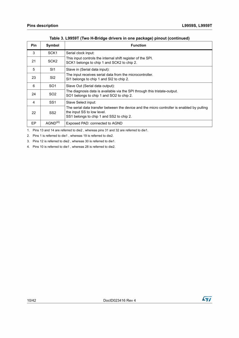
3 SCK1 Serial clock input:
This input controls the internal shift register of the SPI.SCK1 belongs to chip 1 and SCK2 to chip 2.21 SCK2
5 SI1 Slave in (Serial data input):
The input receives serial data from the microcontroller. SI1 belongs to chip 1 and SI2 to chip 2.23 SI2
6 SO1 Slave Out (Serial data output):
The diagnosis data is available via the SPI through this tristate-output. SO1 belongs to chip 1 and SO2 to chip 2.24 SO2
4 SS1 Slave Select input:
The serial data transfer between the device and the micro controller is enabled by pulling the input SS to low level.SS1 belongs to chip 1 and SS2 to chip 2.
22 SS2
EP AGND(4) Exposed PAD: connected to AGND
1. Pins 13 and 14 are referred to die2 , whereas pins 31 and 32 are referred to die1.
2. Pins 1 is referred to die1 , whereas 19 is referred to die2.
3. Pins 12 is referred to die2 , whereas 30 is referred to die1.
4. Pins 10 is referred to die1 , whereas 28 is referred to die2.
Table 3. L9959T (Two H-Bridge drivers in one package) pinout (continued)
Pin Symbol Function

DocID023416 Rev 4 11/42
L9959S, L9959T Electrical specifications
3 Electrical specifications
3.1 Absolute maximum ratings
Warning: Stressing the device above the rating listed in the "Absolute maximum ratings" table may cause permanent damage to the device. These are stress ratings only and operation of the device at these or any other conditions above those indicated in the operating sections of this specification is not implied. Exposure to absolute maximum rating conditions for extended periods may affect device reliability. Refer also to the STMicroelectronics SURE program and other relevant quality document.
3.2 ESD protection
Table 4. Absolute maximum ratings
Symbol Parameter / Test condition Value [DC Voltage] Unit
VVS DC supply voltage -1.0 to +40 V
VVDD Stabilized supply voltage, logic supply -0.3 to 18 V
V3V3 3.3 V Controller output -0.3 to 4.6 V
CF Current feedback output -0.3 to 5 V
VSI, VSCK, VSS, VSO, VDIR, VPWM, VDIS
Logic input / output voltage range -0.3 to 18 V
VOUTn
Output voltage (n=1,2 or 11,12,21,22);
VOUTn < VS + 1 V-1.0 to 40 V
Dynamic pulse / t < 500ms;
VOUTn < VS + 2 V-2.0 to 40 V
Tj Operating junction temperature -40 to 150 °C
Tstg Storage temperature -55 to 150 °C
Table 5. ESD protection
Parameter Value Unit
All pins versus ground group (AGND, PGND1, PGND2, GND_ABE1, GND_ABE2)
±2(1)
1. HBM according to MIL 883C, Method 3015.7 or EIA/JESD22-A114-A.
kV
Power Output Pins: OUT1, OUT2 or OUT11, OUT12, OUT21, OUT22 versus ground group (AGND, PGND1, PGND2, GND_ABE1, GND_ABE2)
±4(2)
2. HBM with all unzipped pins grounded.
kV
Electrical specifications L9959S, L9959T
12/42 DocID023416 Rev 4
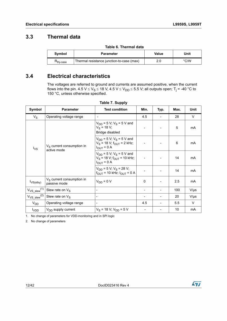
3.3 Thermal data
3.4 Electrical characteristics
The voltages are referred to ground and currents are assumed positive, when the current flows into the pin. 4.5 V VS 18 V, 4.5 V VDD 5.5 V; all outputs open; Tj = -40 °C to 150 °C, unless otherwise specified.
Table 6. Thermal data
Symbol Parameter Value Unit
Rthj-case Thermal resistance junction-to-case (max) 2.0 °C/W
Table 7. Supply
Symbol Parameter Test condition Min. Typ. Max. Unit
VS Operating voltage range - 4.5 - 28 V
IVSVS current consumption in active mode
VDD = 5 V; VS = 5 V and VS = 18 V;
Bridge disabled- - 5 mA
VDD = 5 V; VS = 5 V and VS = 18 V; fOUT = 2 kHz; IOUT = 0 A
- - 6 mA
VDD = 5 V; VS = 5 V and VS = 18 V; fOUT = 10 kHz; IOUT = 0 A
- - 14 mA
VDD = 5 V; VS = 28 V; fOUT = 10 kHz; IOUT = 0 A
- - 14 mA
IVS(stby)VS current consumption in passive mode
VDD = 0 V 0 - 2.5 mA
VVS_slew(1) Slew rate on VS - - - 100 V/µs
VVS_slew(2) Slew rate on VS - - - 20 V/µs
VDD Operating voltage range - 4.5 - 5.5 V
IVDD VDD supply current VS = 18 V; VDD = 5 V - - 10 mA
1. No change of parameters for VDD-monitoring and in SPI logic
2. No change of parameters
DocID023416 Rev 4 13/42
L9959S, L9959T Electrical specifications
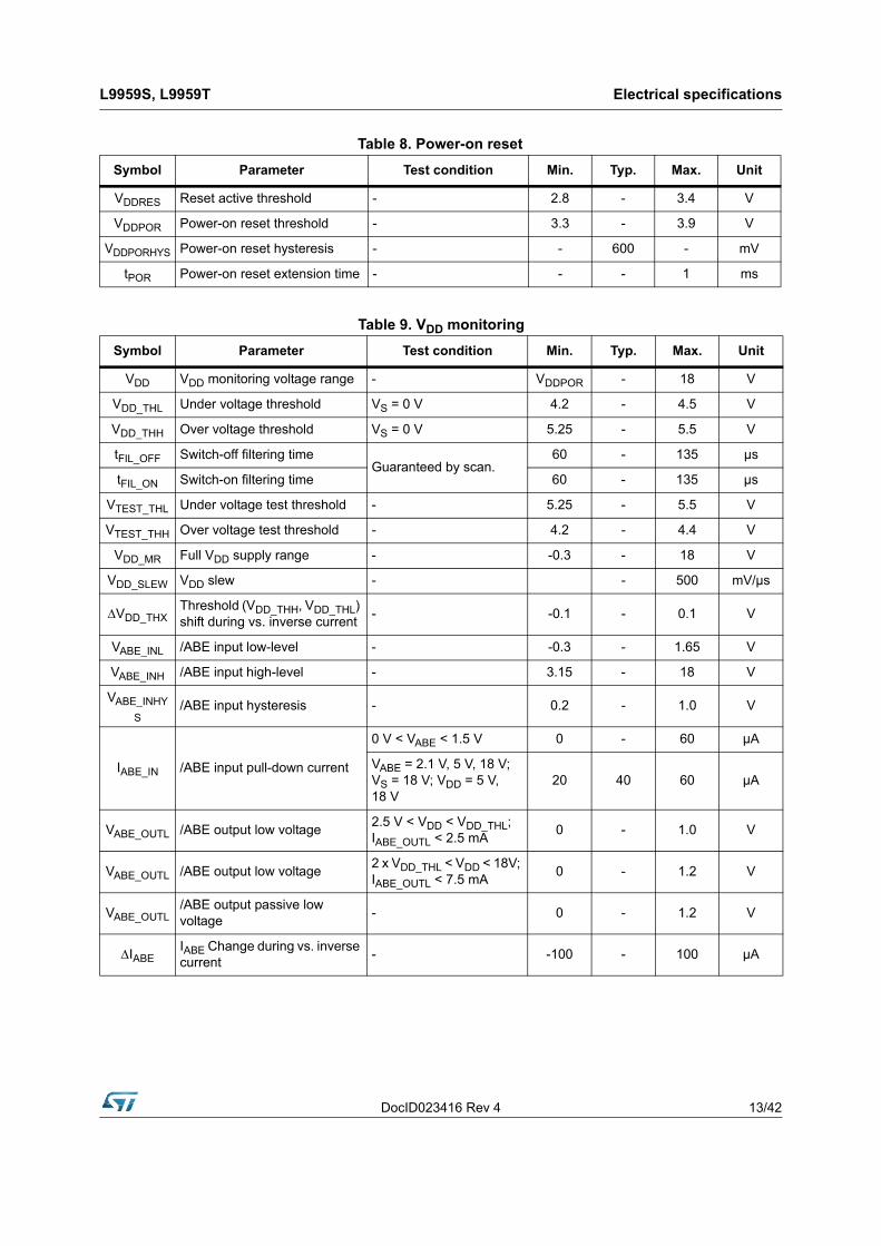
Table 8. Power-on reset
Symbol Parameter Test condition Min. Typ. Max. Unit
VDDRES Reset active threshold - 2.8 - 3.4 V
VDDPOR Power-on reset threshold - 3.3 - 3.9 V
VDDPORHYS Power-on reset hysteresis - - 600 - mV
tPOR Power-on reset extension time - - - 1 ms
Table 9. VDD monitoring
Symbol Parameter Test condition Min. Typ. Max. Unit
VDD VDD monitoring voltage range - VDDPOR - 18 V
VDD_THL Under voltage threshold VS = 0 V 4.2 - 4.5 V
VDD_THH Over voltage threshold VS = 0 V 5.25 - 5.5 V
tFIL_OFF Switch-off filtering time Guaranteed by scan.
60 - 135 µs
tFIL_ON Switch-on filtering time 60 - 135 µs
VTEST_THL Under voltage test threshold - 5.25 - 5.5 V
VTEST_THH Over voltage test threshold - 4.2 - 4.4 V
VDD_MR Full VDD supply range - -0.3 - 18 V
VDD_SLEW VDD slew - - 500 mV/µs
VDD_THXThreshold (VDD_THH, VDD_THL) shift during vs. inverse current
- -0.1 - 0.1 V
VABE_INL /ABE input low-level - -0.3 - 1.65 V
VABE_INH /ABE input high-level - 3.15 - 18 V
VABE_INHY
S/ABE input hysteresis - 0.2 - 1.0 V
IABE_IN /ABE input pull-down current
0 V < VABE < 1.5 V 0 - 60 µA
VABE = 2.1 V, 5 V, 18 V; VS = 18 V; VDD = 5 V, 18 V
20 40 60 µA
VABE_OUTL /ABE output low voltage 2.5 V < VDD < VDD_THL; IABE_OUTL < 2.5 mA
0 - 1.0 V
VABE_OUTL /ABE output low voltage 2 x VDD_THL < VDD < 18V; IABE_OUTL < 7.5 mA
0 - 1.2 V
VABE_OUTL/ABE output passive low voltage
- 0 - 1.2 V
IABEIABE Change during vs. inverse current
- -100 - 100 µA
Electrical specifications L9959S, L9959T
14/42 DocID023416 Rev 4
3.5 Outputs OUT1 and OUT2
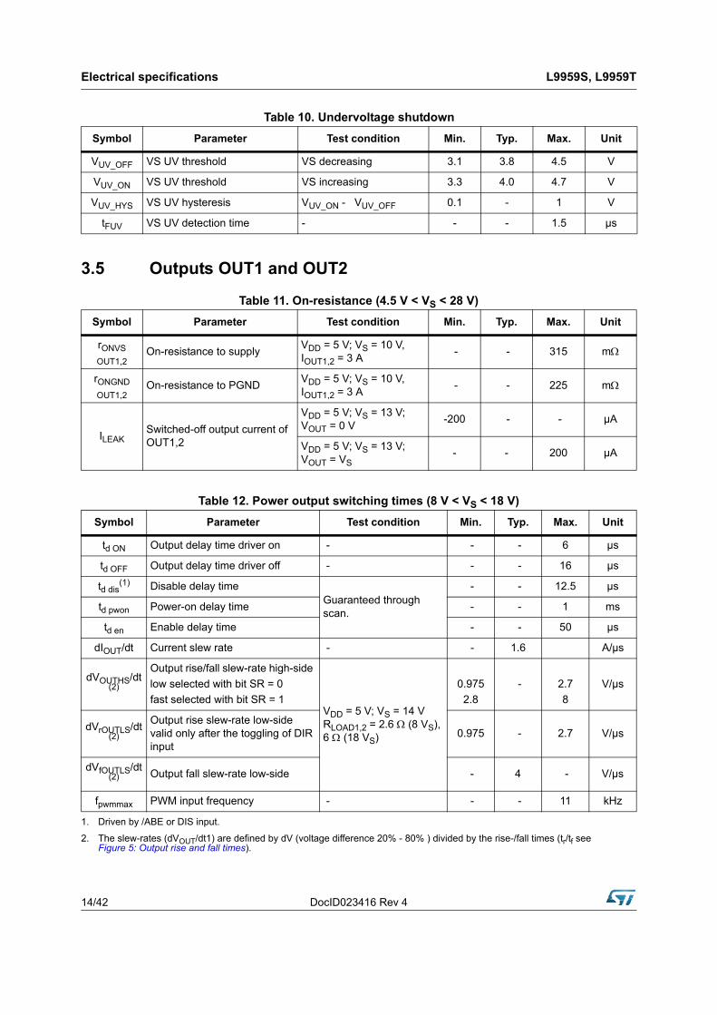
Table 10. Undervoltage shutdown
Symbol Parameter Test condition Min. Typ. Max. Unit
VUV_OFF VS UV threshold VS decreasing 3.1 3.8 4.5 V
VUV_ON VS UV threshold VS increasing 3.3 4.0 4.7 V
VUV_HYS VS UV hysteresis VUV_ON - VUV_OFF 0.1 - 1 V
tFUV VS UV detection time - - - 1.5 µs
Table 11. On-resistance (4.5 V < VS < 28 V)
Symbol Parameter Test condition Min. Typ. Max. Unit
rONVS
OUT1,2 On-resistance to supply
VDD = 5 V; VS = 10 V, IOUT1,2 = 3 A
- - 315 m
rONGND
OUT1,2 On-resistance to PGND
VDD = 5 V; VS = 10 V, IOUT1,2 = 3 A
- - 225 m
ILEAK Switched-off output current of OUT1,2
VDD = 5 V; VS = 13 V; VOUT = 0 V
-200 - - µA
VDD = 5 V; VS = 13 V; VOUT = VS
- - 200 µA
Table 12. Power output switching times (8 V < VS < 18 V)
Symbol Parameter Test condition Min. Typ. Max. Unit
td ON Output delay time driver on - - - 6 µs
td OFF Output delay time driver off - - - 16 µs
td dis(1) Disable delay time
Guaranteed through scan.
- - 12.5 µs
td pwon Power-on delay time - - 1 ms
td en Enable delay time - - 50 µs
dIOUT/dt Current slew rate - - 1.6 A/µs
dVOUTHS/dt(2)
Output rise/fall slew-rate high-side
low selected with bit SR = 0
fast selected with bit SR = 1VDD = 5 V; VS = 14 V RLOAD1,2 = 2.6 (8 VS), 6 (18 VS)
0.975
2.8
- 2.7
8
V/µs
dVrOUTLS/dt(2)
Output rise slew-rate low-side valid only after the toggling of DIR input
0.975 - 2.7 V/µs
dVfOUTLS/dt(2)
Output fall slew-rate low-side - 4 - V/µs
fpwmmax PWM input frequency - - - 11 kHz
1. Driven by /ABE or DIS input.
2. The slew-rates (dVOUT/dt1) are defined by dV (voltage difference 20% - 80% ) divided by the rise-/fall times (tr/tf see Figure 5: Output rise and fall times).
DocID023416 Rev 4 15/42
L9959S, L9959T Electrical specifications
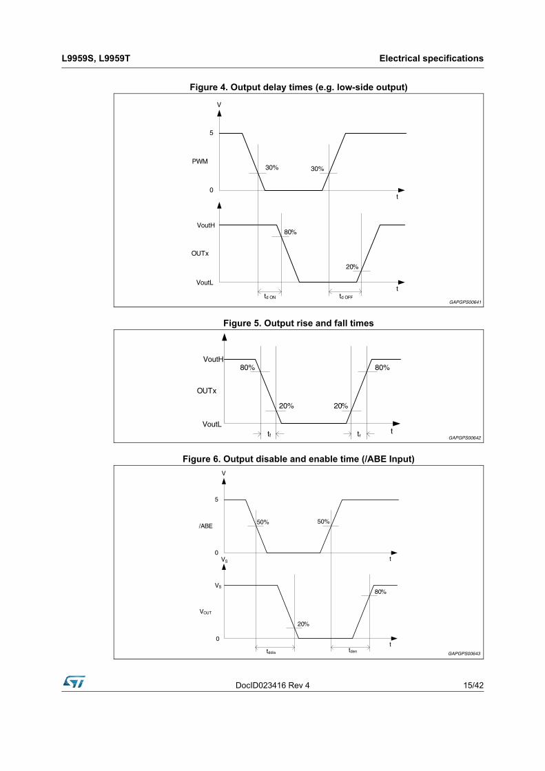
Figure 4. Output delay times (e.g. low-side output)
Figure 5. Output rise and fall times
Figure 6. Output disable and enable time (/ABE Input)
Electrical specifications L9959S, L9959T
16/42 DocID023416 Rev 4
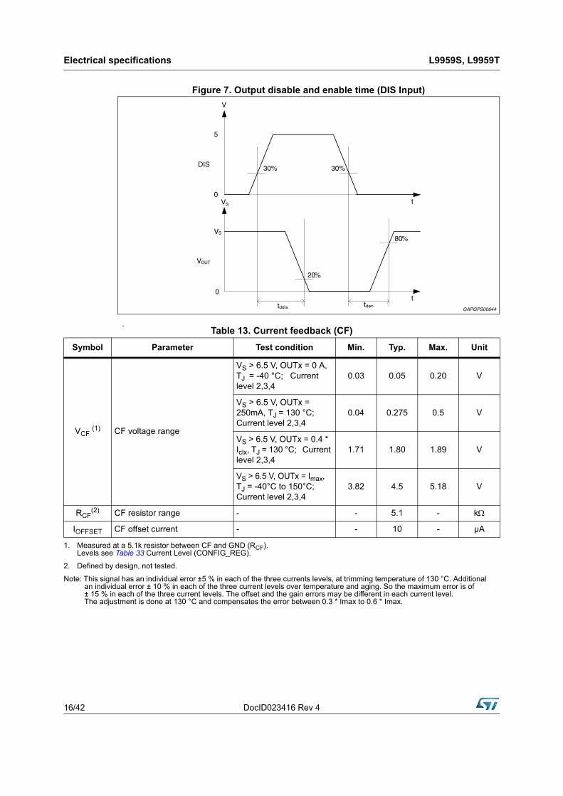
Figure 7. Output disable and enable time (DIS Input)
N
Table 13. Current feedback (CF)
Symbol Parameter Test condition Min. Typ. Max. Unit
VCF (1) CF voltage range
VS > 6.5 V, OUTx = 0 A, TJ = -40 °C; Current level 2,3,4
0.03 0.05 0.20 V
VS > 6.5 V, OUTx = 250mA, TJ = 130 °C; Current level 2,3,4
0.04 0.275 0.5 V
VS > 6.5 V, OUTx = 0.4 * Iclx, TJ = 130 °C; Current level 2,3,4
1.71 1.80 1.89 V
VS > 6.5 V, OUTx = Imax, TJ = -40°C to 150°C; Current level 2,3,4
3.82 4.5 5.18 V
RCF(2) CF resistor range - - 5.1 - k
IOFFSET CF offset current - - 10 - µA
1. Measured at a 5.1k resistor between CF and GND (RCF).Levels see Table 33 Current Level (CONFIG_REG).
2. Defined by design, not tested.
Note: This signal has an individual error ±5 % in each of the three currents levels, at trimming temperature of 130 °C. Additionalan individual error ± 10 % in each of the three current levels over temperature and aging. So the maximum error is of± 15 % in each of the three current levels. The offset and the gain errors may be different in each current level.The adjustment is done at 130 °C and compensates the error between 0.3 * Imax to 0.6 * Imax.
DocID023416 Rev 4 17/42
L9959S, L9959T Electrical specifications
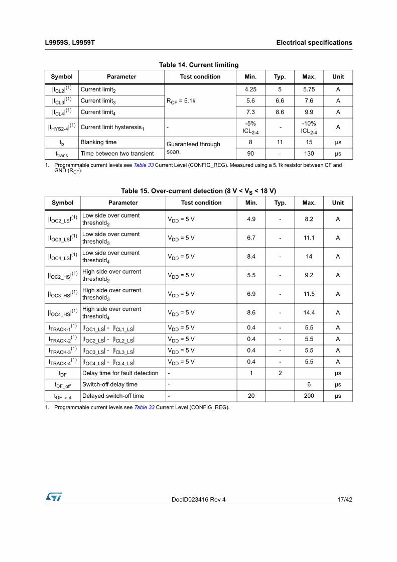
Table 14. Current limiting
Symbol Parameter Test condition Min. Typ. Max. Unit
|ICL2|(1) Current limit2
RCF = 5.1k
4.25 5 5.75 A
|ICL3|(1) Current limit3 5.6 6.6 7.6 A
|ICL4|(1) Current limit4 7.3 8.6 9.9 A
|IHYS2-4|(1) Current limit hysteresis1 --5%
ICL2-4 -
-10% ICL2-4
A
tb Blanking time Guaranteed through scan.
8 11 15 µs
ttrans Time between two transient 90 - 130 µs
1. Programmable current levels see Table 33 Current Level (CONFIG_REG). Measured using a 5.1k resistor between CF and GND (RCF).
Table 15. Over-current detection (8 V < VS < 18 V)
Symbol Parameter Test condition Min. Typ. Max. Unit
|IOC2_LSI(1) Low side over current threshold2
VDD = 5 V 4.9 - 8.2 A
|IOC3_LS|(1) Low side over current threshold3
VDD = 5 V 6.7 - 11.1 A
|IOC4_LS|(1) Low side over current threshold4
VDD = 5 V 8.4 - 14 A
|IOC2_HSI(1) High side over current threshold2
VDD = 5 V 5.5 - 9.2 A
|IOC3_HS|(1) High side over current threshold3
VDD = 5 V 6.9 - 11.5 A
|IOC4_HS|(1) High side over current threshold4
VDD = 5 V 8.6 - 14.4 A
ITRACK-1(1) |IOC1_LS| - |ICL1_LS| VDD = 5 V 0.4 - 5.5 A
ITRACK-2(1) |IOC2_LS| - |ICL2_LS| VDD = 5 V 0.4 - 5.5 A
ITRACK-3(1) |IOC3_LS| - |ICL3_LS| VDD = 5 V 0.4 - 5.5 A
ITRACK-4(1) |IOC4_LS| - |ICL4_LS| VDD = 5 V 0.4 - 5.5 A
tDF Delay time for fault detection - 1 2 µs
tDF_off Switch-off delay time - 6 µs
tDF_del Delayed switch-off time - 20 200 µs
1. Programmable current levels see Table 33 Current Level (CONFIG_REG).
Electrical specifications L9959S, L9959T
18/42 DocID023416 Rev 4
3.6 Temperature dependent current reduction
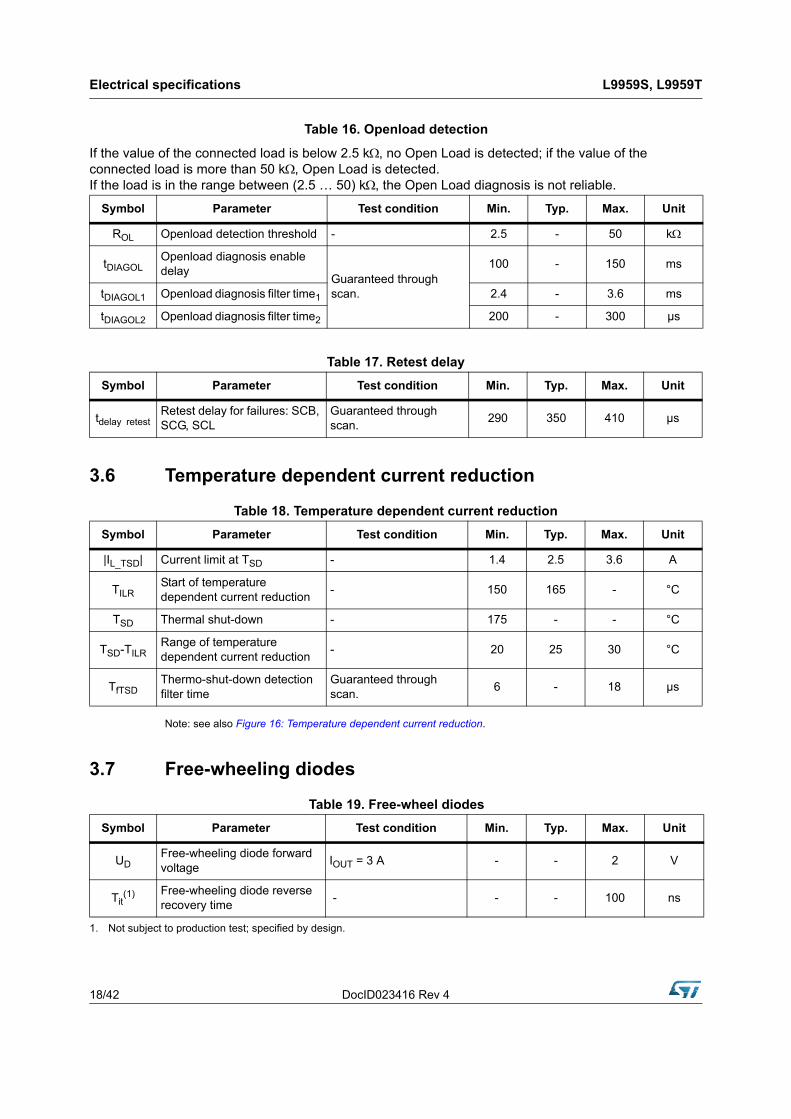
Note: see also Figure 16: Temperature dependent current reduction.
3.7 Free-wheeling diodes
Table 16. Openload detection
If the value of the connected load is below 2.5 k, no Open Load is detected; if the value of the connected load is more than 50 k, Open Load is detected.If the load is in the range between (2.5 … 50) k, the Open Load diagnosis is not reliable.
Symbol Parameter Test condition Min. Typ. Max. Unit
ROL Openload detection threshold - 2.5 - 50 k
tDIAGOLOpenload diagnosis enable delay
Guaranteed through scan.
100 - 150 ms
tDIAGOL1 Openload diagnosis filter time1 2.4 - 3.6 ms
tDIAGOL2 Openload diagnosis filter time2 200 - 300 µs
Table 17. Retest delay
Symbol Parameter Test condition Min. Typ. Max. Unit
tdelay retest Retest delay for failures: SCB, SCG, SCL
Guaranteed through scan.
290 350 410 µs
Table 18. Temperature dependent current reduction
Symbol Parameter Test condition Min. Typ. Max. Unit
|IL_TSD| Current limit at TSD - 1.4 2.5 3.6 A
TILRStart of temperature dependent current reduction
- 150 165 - °C
TSD Thermal shut-down - 175 - - °C
TSD-TILRRange of temperature dependent current reduction
- 20 25 30 °C
TfTSDThermo-shut-down detection filter time
Guaranteed through scan.
6 - 18 µs
Table 19. Free-wheel diodes
Symbol Parameter Test condition Min. Typ. Max. Unit
UDFree-wheeling diode forward voltage
IOUT = 3 A - - 2 V
Tit(1) Free-wheeling diode reverse
recovery time - - - 100 ns
1. Not subject to production test; specified by design.
DocID023416 Rev 4 19/42
L9959S, L9959T Electrical specifications
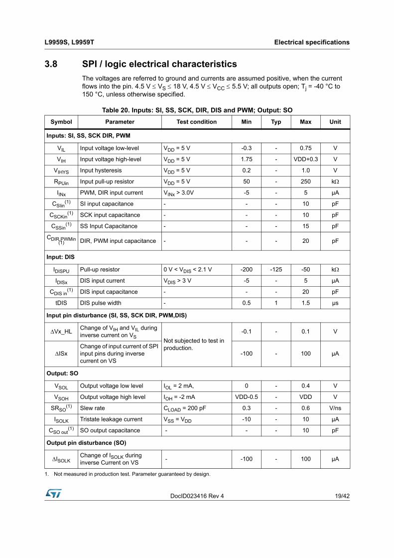
3.8 SPI / logic electrical characteristics
The voltages are referred to ground and currents are assumed positive, when the current flows into the pin. 4.5 V VS 18 V, 4.5 V VCC 5.5 V; all outputs open; Tj = -40 °C to 150 °C, unless otherwise specified.
Table 20. Inputs: SI, SS, SCK, DIR, DIS and PWM; Output: SO
Symbol Parameter Test condition Min Typ Max Unit
Inputs: SI, SS, SCK DIR, PWM
VIL Input voltage low-level VDD = 5 V -0.3 - 0.75 V
VIH Input voltage high-level VDD = 5 V 1.75 - VDD+0.3 V
VIHYS Input hysteresis VDD = 5 V 0.2 - 1.0 V
RPUin Input pull-up resistor VDD = 5 V 50 - 250 k
IINx PWM, DIR input current VINx > 3.0V -5 - 5 µA
CSIin(1) SI input capacitance - - - 10 pF
CSCKin(1) SCK input capacitance - - - 10 pF
CSSin(1) SS Input Capacitance - - - 15 pF
CDIR,PWMin(1) DIR, PWM input capacitance - - - 20 pF
Input: DIS
IDISPU Pull-up resistor 0 V < VDIS < 2.1 V -200 -125 -50 k
IDISx DIS input current VDIS > 3 V -5 - 5 µA
CDIS in(1) DIS input capacitance - - - 20 pF
tDIS DIS pulse width - 0.5 1 1.5 µs
Input pin disturbance (SI, SS, SCK DIR, PWM,DIS)
Vx_HL Change of VIH and VIL during inverse current on VS
Not subjected to test in production.
-0.1 - 0.1 V
ISx Change of input current of SPI input pins during inverse current on VS
-100 - 100 µA
Output: SO
VSOL Output voltage low level IOL = 2 mA, 0 - 0.4 V
VSOH Output voltage high level IOH = -2 mA VDD-0.5 - VDD V
SRSO(1) Slew rate CLOAD = 200 pF 0.3 - 0.6 V/ns
ISOLK Tristate leakage current VSS = VDD -10 - 10 µA
CSO out(1) SO output capacitance - - - 10 pF
Output pin disturbance (SO)
ISOLK Change of ISOLK during inverse Current on VS
- -100 - 100 µA
1. Not measured in production test. Parameter guaranteed by design.
Electrical specifications L9959S, L9959T
20/42 DocID023416 Rev 4
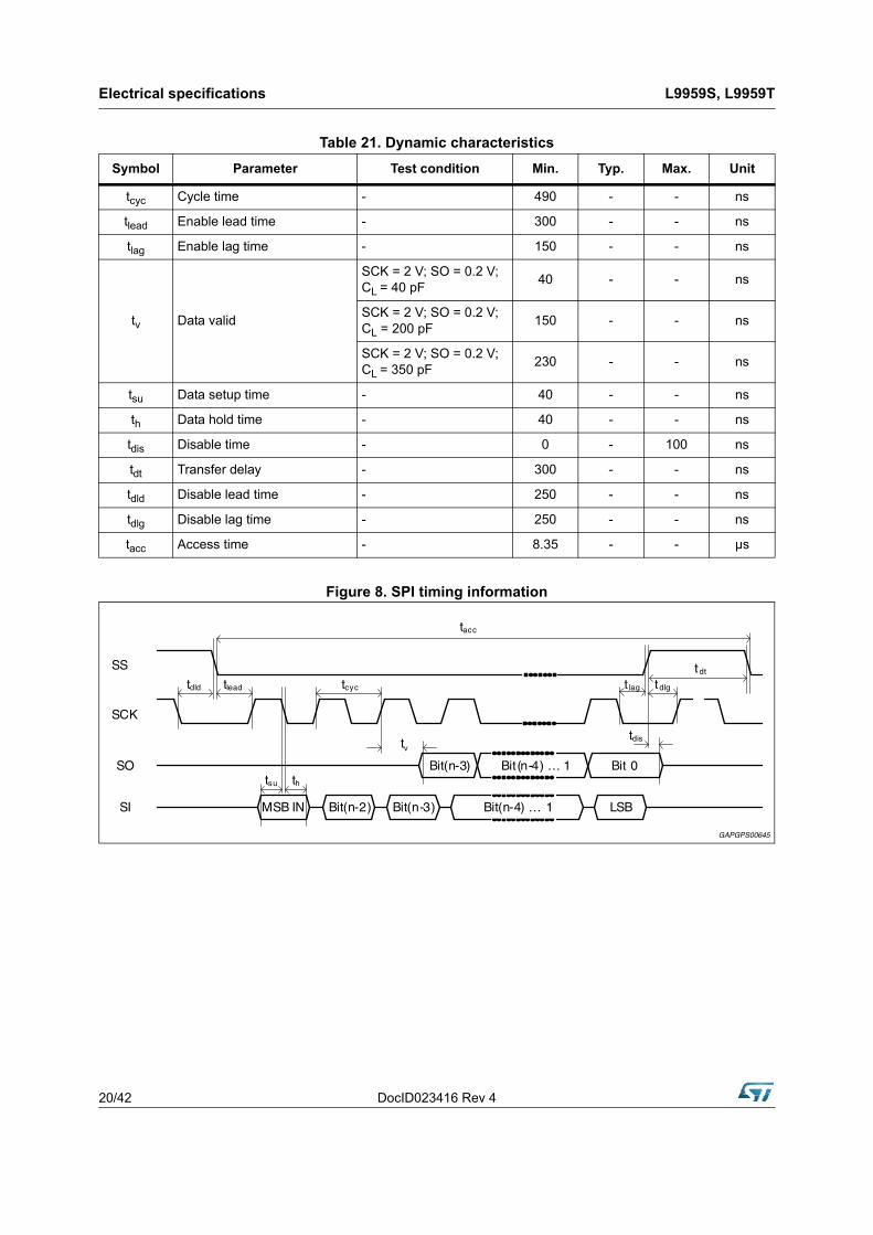
Figure 8. SPI timing information
Table 21. Dynamic characteristics
Symbol Parameter Test condition Min. Typ. Max. Unit
tcyc Cycle time - 490 - - ns
tlead Enable lead time - 300 - - ns
tlag Enable lag time - 150 - - ns
tv Data valid
SCK = 2 V; SO = 0.2 V; CL = 40 pF
40 - - ns
SCK = 2 V; SO = 0.2 V; CL = 200 pF
150 - - ns
SCK = 2 V; SO = 0.2 V; CL = 350 pF
230 - - ns
tsu Data setup time - 40 - - ns
th Data hold time - 40 - - ns
tdis Disable time - 0 - 100 ns
tdt Transfer delay - 300 - - ns
tdld Disable lead time - 250 - - ns
tdlg Disable lag time - 250 - - ns
tacc Access time - 8.35 - - µs
DocID023416 Rev 4 21/42
L9959S, L9959T Application information
4 Application information
4.1 Power stage switching behavior
The L9959 output stages can either be controlled by the pins PWM and DIR or by their corresponding SPI registers (SPWM and SDIR: see Table 32: Configuration register (CONFIG_REG)). The SPI bit MUX in the configuration register (CONFIG_REG) determines this. If the power stages are disabled by /ABE or DIS, this bit is reset and the pins PWM and DIR control the outputs.
The active free-wheeling, in which the body diode is actively shorted by its associated Power-MOS, can be disabled by the bit FW in the configuration register. By default, active free-wheeling is enabled.
The device minimizes electro-magnetic emission by switching the high-side and low-side drivers in a special sequence. Two cases are distinguished: The PWM-mode, during which the current direction does not change and the direction switch using the DIR, which changes the current direction (see Figure 9, Figure 11 and Figure 12).
4.1.1 PWM mode (same current direction)
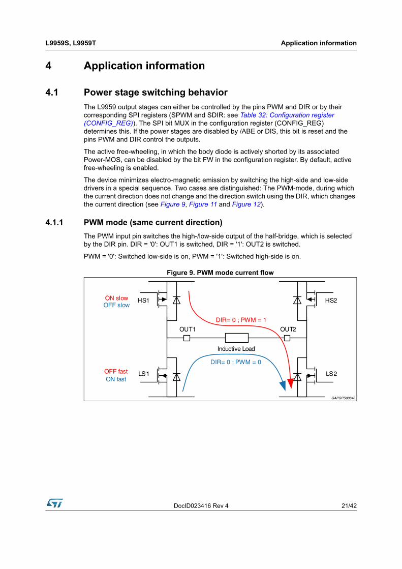
The PWM input pin switches the high-/low-side output of the half-bridge, which is selected by the DIR pin. DIR = '0': OUT1 is switched, DIR = '1': OUT2 is switched.
PWM = '0': Switched low-side is on, PWM = '1': Switched high-side is on.
Figure 9. PWM mode current flow
Application information L9959S, L9959T
22/42 DocID023416 Rev 4
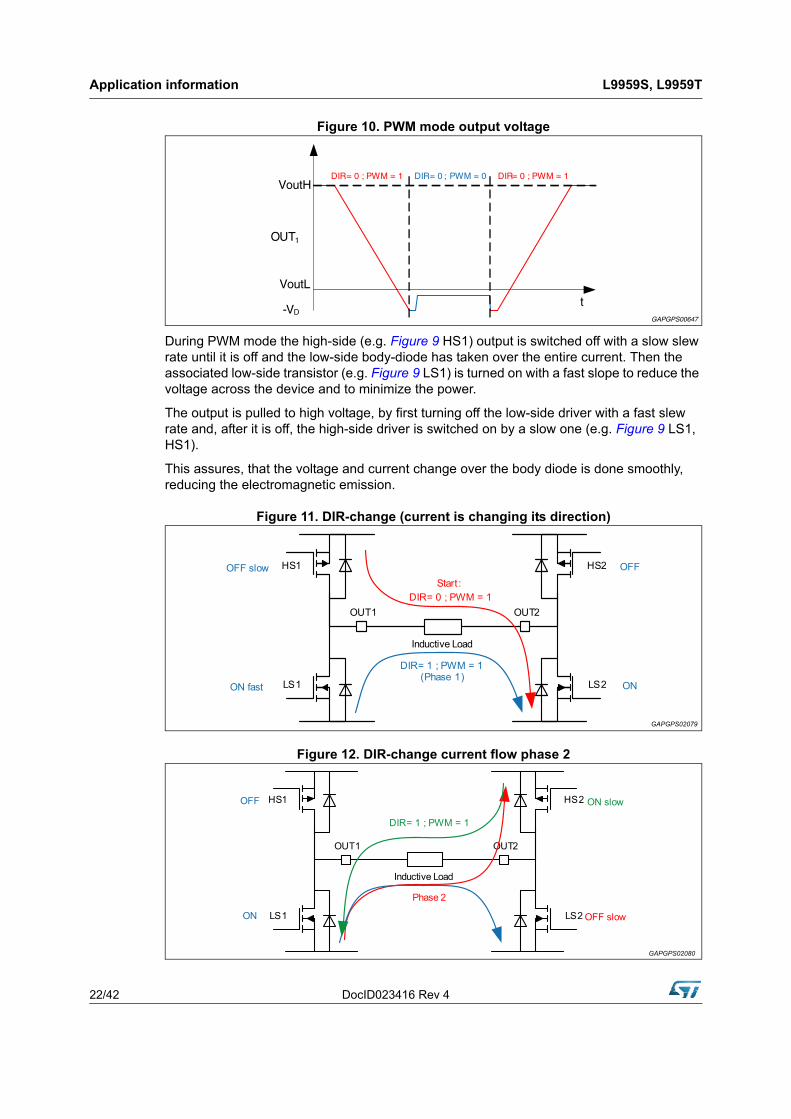
Figure 10. PWM mode output voltage
During PWM mode the high-side (e.g. Figure 9 HS1) output is switched off with a slow slew rate until it is off and the low-side body-diode has taken over the entire current. Then the associated low-side transistor (e.g. Figure 9 LS1) is turned on with a fast slope to reduce the voltage across the device and to minimize the power.
The output is pulled to high voltage, by first turning off the low-side driver with a fast slew rate and, after it is off, the high-side driver is switched on by a slow one (e.g. Figure 9 LS1, HS1).
This assures, that the voltage and current change over the body diode is done smoothly, reducing the electromagnetic emission.
Figure 11. DIR-change (current is changing its direction)
Figure 12. DIR-change current flow phase 2
DocID023416 Rev 4 23/42
L9959S, L9959T Application information
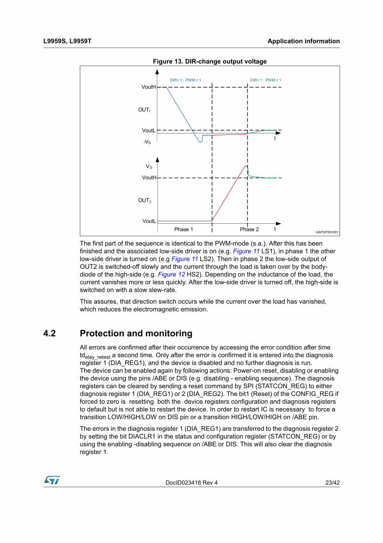
Figure 13. DIR-change output voltage
The first part of the sequence is identical to the PWM-mode (s.a.). After this has been finished and the associated low-side driver is on (e.g. Figure 11 LS1), in phase 1 the other low-side driver is turned on (e.g Figure 11 LS2). Then in phase 2 the low-side output of OUT2 is switched-off slowly and the current through the load is taken over by the body-diode of the high-side (e.g. Figure 12 HS2). Depending on the inductance of the load, the current vanishes more or less quickly. After the low-side driver is turned off, the high-side is switched on with a slow slew-rate.
This assures, that direction switch occurs while the current over the load has vanished, which reduces the electromagnetic emission.
4.2 Protection and monitoring
All errors are confirmed after their occurrence by accessing the error condition after time tdelay_retest a second time. Only after the error is confirmed it is entered into the diagnosis register 1 (DIA_REG1), and the device is disabled and no further diagnosis is run.The device can be enabled again by following actions: Power-on reset, disabling or enabling the device using the pins /ABE or DIS (e.g. disabling - enabling sequence). The diagnosis registers can be cleared by sending a reset command by SPI (STATCON_REG) to either diagnosis register 1 (DIA_REG1) or 2 (DIA_REG2). The bit1 (Reset) of the CONFIG_REG if forced to zero is resetting both the device registers configuration and diagnosis registers to default but is not able to restart the device. In order to restart IC is necessary to force a transition LOW/HIGH/LOW on DIS pin or a transition HIGH/LOW/HIGH on /ABE pin.
The errors in the diagnosis register 1 (DIA_REG1) are transferred to the diagnosis register 2 by setting the bit DIACLR1 in the status and configuration register (STATCON_REG) or by using the enabling -disabling sequence on /ABE or DIS. This will also clear the diagnosis register 1.
Application information L9959S, L9959T
24/42 DocID023416 Rev 4
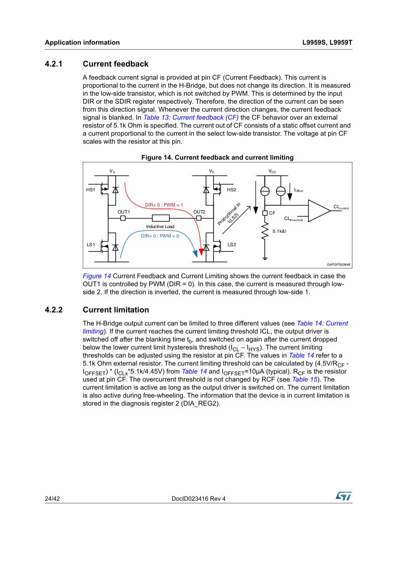
4.2.1 Current feedback
A feedback current signal is provided at pin CF (Current Feedback). This current is proportional to the current in the H-Bridge, but does not change its direction. It is measured in the low-side transistor, which is not switched by PWM. This is determined by the input DIR or the SDIR register respectively. Therefore, the direction of the current can be seen from this direction signal. Whenever the current direction changes, the current feedback signal is blanked. In Table 13: Current feedback (CF) the CF behavior over an external resistor of 5.1k Ohm is specified. The current out of CF consists of a static offset current and a current proportional to the current in the select low-side transistor. The voltage at pin CF scales with the resistor at this pin.
Figure 14. Current feedback and current limiting
Figure 14 Current Feedback and Current Limiting shows the current feedback in case the OUT1 is controlled by PWM (DIR = 0). In this case, the current is measured through low-side 2. If the direction is inverted, the current is measured through low-side 1.
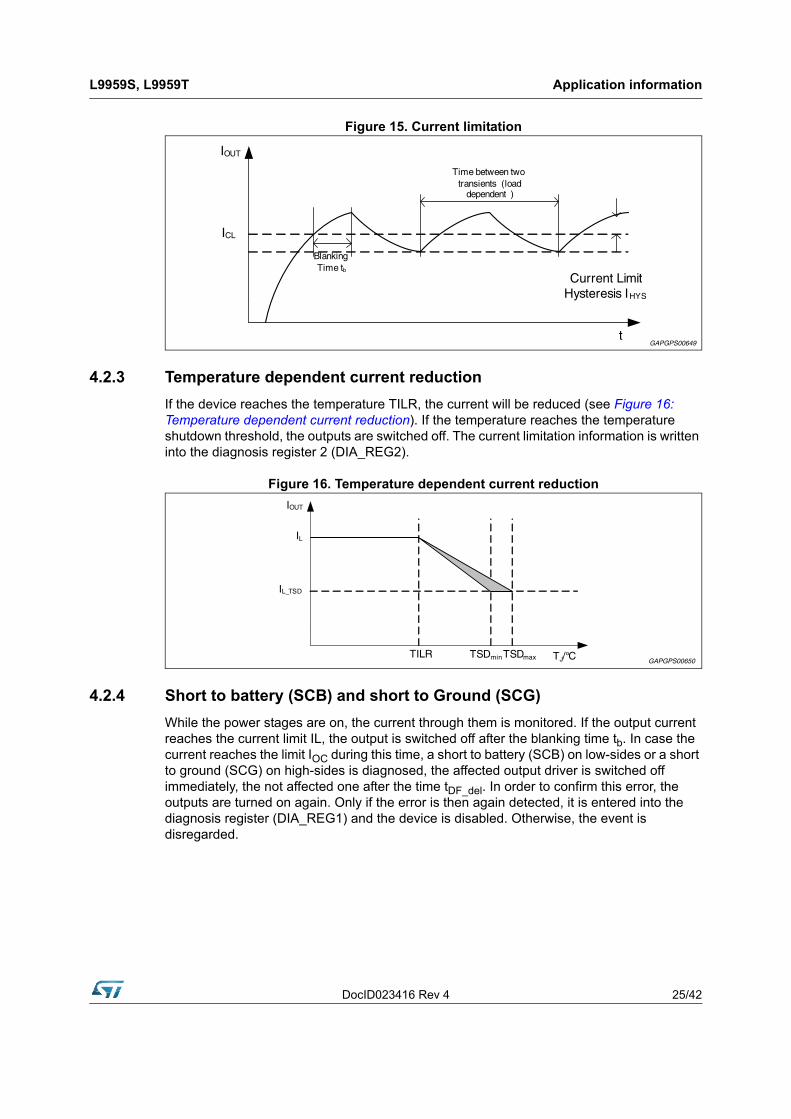
4.2.2 Current limitation
The H-Bridge output current can be limited to three different values (see Table 14: Current limiting). If the current reaches the current limiting threshold ICL, the output driver is switched off after the blanking time tb, and switched on again after the current dropped below the lower current limit hysteresis threshold (ICL – IHYS). The current limiting thresholds can be adjusted using the resistor at pin CF. The values in Table 14 refer to a 5.1k Ohm external resistor. The current limiting threshold can be calculated by (4.5V/RCF - IOFFSET) * (ICLx*5.1k/4.45V) from Table 14 and IOFFSET=10µA (typical). RCF is the resistor used at pin CF. The overcurrent threshold is not changed by RCF (see Table 15). The current limitation is active as long as the output driver is switched on. The current limitation is also active during free-wheeling. The information that the device is in current limitation is stored in the diagnosis register 2 (DIA_REG2).
DocID023416 Rev 4 25/42
L9959S, L9959T Application information
Figure 15. Current limitation
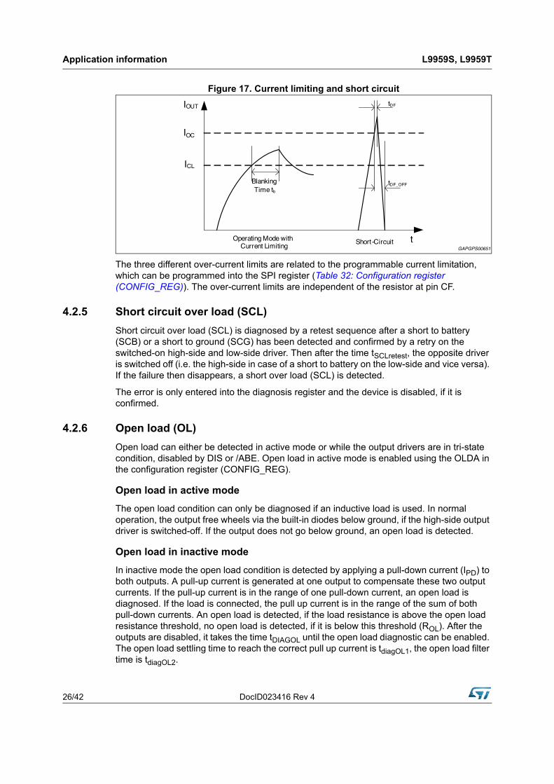
4.2.3 Temperature dependent current reduction
If the device reaches the temperature TILR, the current will be reduced (see Figure 16: Temperature dependent current reduction). If the temperature reaches the temperature shutdown threshold, the outputs are switched off. The current limitation information is written into the diagnosis register 2 (DIA_REG2).
Figure 16. Temperature dependent current reduction
4.2.4 Short to battery (SCB) and short to Ground (SCG)
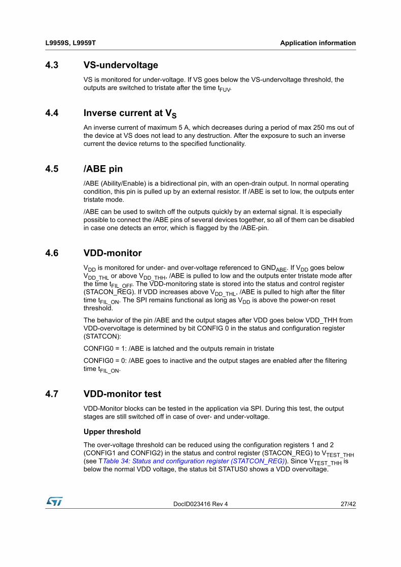
While the power stages are on, the current through them is monitored. If the output current reaches the current limit IL, the output is switched off after the blanking time tb. In case the current reaches the limit IOC during this time, a short to battery (SCB) on low-sides or a short to ground (SCG) on high-sides is diagnosed, the affected output driver is switched off immediately, the not affected one after the time tDF_del. In order to confirm this error, the outputs are turned on again. Only if the error is then again detected, it is entered into the diagnosis register (DIA_REG1) and the device is disabled. Otherwise, the event is disregarded.
Application information L9959S, L9959T
26/42 DocID023416 Rev 4
Figure 17. Current limiting and short circuit
The three different over-current limits are related to the programmable current limitation, which can be programmed into the SPI register (Table 32: Configuration register (CONFIG_REG)). The over-current limits are independent of the resistor at pin CF.
4.2.5 Short circuit over load (SCL)
Short circuit over load (SCL) is diagnosed by a retest sequence after a short to battery (SCB) or a short to ground (SCG) has been detected and confirmed by a retry on the switched-on high-side and low-side driver. Then after the time tSCLretest, the opposite driver is switched off (i.e. the high-side in case of a short to battery on the low-side and vice versa). If the failure then disappears, a short over load (SCL) is detected.
The error is only entered into the diagnosis register and the device is disabled, if it is confirmed.
4.2.6 Open load (OL)
Open load can either be detected in active mode or while the output drivers are in tri-state condition, disabled by DIS or /ABE. Open load in active mode is enabled using the OLDA in the configuration register (CONFIG_REG).
Open load in active mode
The open load condition can only be diagnosed if an inductive load is used. In normal operation, the output free wheels via the built-in diodes below ground, if the high-side output driver is switched-off. If the output does not go below ground, an open load is detected.
Open load in inactive mode
In inactive mode the open load condition is detected by applying a pull-down current (IPD) to both outputs. A pull-up current is generated at one output to compensate these two output currents. If the pull-up current is in the range of one pull-down current, an open load is diagnosed. If the load is connected, the pull up current is in the range of the sum of both pull-down currents. An open load is detected, if the load resistance is above the open load resistance threshold, no open load is detected, if it is below this threshold (ROL). After the outputs are disabled, it takes the time tDIAGOL until the open load diagnostic can be enabled. The open load settling time to reach the correct pull up current is tdiagOL1, the open load filter time is tdiagOL2.
DocID023416 Rev 4 27/42
L9959S, L9959T Application information
4.3 VS-undervoltage
VS is monitored for under-voltage. If VS goes below the VS-undervoltage threshold, the outputs are switched to tristate after the time tFUV.
4.4 Inverse current at VS
An inverse current of maximum 5 A, which decreases during a period of max 250 ms out of the device at VS does not lead to any destruction. After the exposure to such an inverse current the device returns to the specified functionality.
4.5 /ABE pin
/ABE (Ability/Enable) is a bidirectional pin, with an open-drain output. In normal operating condition, this pin is pulled up by an external resistor. If /ABE is set to low, the outputs enter tristate mode.
/ABE can be used to switch off the outputs quickly by an external signal. It is especially possible to connect the /ABE pins of several devices together, so all of them can be disabled in case one detects an error, which is flagged by the /ABE-pin.
4.6 VDD-monitor
VDD is monitored for under- and over-voltage referenced to GNDABE. If VDD goes below VDD_THL or above VDD_THH, /ABE is pulled to low and the outputs enter tristate mode after the time tFIL_OFF. The VDD-monitoring state is stored into the status and control register (STACON_REG). If VDD increases above VDD_THL, /ABE is pulled to high after the filter time tFIL_ON. The SPI remains functional as long as VDD is above the power-on reset threshold.
The behavior of the pin /ABE and the output stages after VDD goes below VDD_THH from VDD-overvoltage is determined by bit CONFIG 0 in the status and configuration register (STATCON):
CONFIG0 = 1: /ABE is latched and the outputs remain in tristate
CONFIG0 = 0: /ABE goes to inactive and the output stages are enabled after the filtering time tFIL_ON.
4.7 VDD-monitor test
VDD-Monitor blocks can be tested in the application via SPI. During this test, the output stages are still switched off in case of over- and under-voltage.
Upper threshold
The over-voltage threshold can be reduced using the configuration registers 1 and 2 (CONFIG1 and CONFIG2) in the status and control register (STACON_REG) to VTEST_THH (see TTable 34: Status and configuration register (STATCON_REG)). Since VTEST_THH is below the normal VDD voltage, the status bit STATUS0 shows a VDD overvoltage.
Application information L9959S, L9959T
28/42 DocID023416 Rev 4
Lower threshold
The under-voltage threshold can be increased to VTEST_THL using CONFIG1 and CONFIG2 in the STATCON register. Since the VDD voltage is below VTEST_THL, the resulting VDD-undervoltage resets STATUS0.
After leaving the VDD-monitor test mode, the bits in the STACON register return to their normal state.
4.8 Power-on reset
At power-on, while VDD increases, the internal registers are cleared and the outputs are set to tristate at the reset-active voltage VDDRES. Above the power-on reset threshold VDDPOR the device starts to operate after the time tPOR. If VDD drops below VDDPOR, the device enters its reset state, i.e. all internal registers are cleared and the outputs are set to tristate.
Note: All voltages are nominal. Please refer to Section 3: Electrical specifications for their specified values.
Table 22. Device states with respect to supply voltage
VS [V] VDD [V] Functional state
28 – 40 0 – 18 No damage to the device, no functional behavior guaranteed
4.5 – 6.5 4.5 – 5.5 Device functional, Current Feedback accuracy reduced
6.5 – 28 4.5 – 5.5 Device functional
4.5 – 28 4.0 – 4.5 5.5 - 18 Device functional, but power-outputs tristate by VDD-monitor, /ABE pulled to low, SPI functional
0 – 4.5 4.5 – 28 VDDPOR – 4.5 Device in reset mode, SPI functional, power-outputs tristate, /ABE pulled to low
0 – 4.5 4.5 – 28 2.5 - VDDPOR Device in reset mode, SPI reset, power-outputs tristate, /ABE tristate
0 – 4.5 4.5 – 5.5 Device functional, outputs are tristate by VS-undervoltage
0 – 4.5 4.0 – 4.5 5.5 - 18 Device functional, outputs are tristate by VS-undervoltage and VDD-monitor, /ABE pulled to low
DocID023416 Rev 4 29/42
L9959S, L9959T SPI functional description
5 SPI functional description
5.1 General description
The SPI communication is based on a Serial Peripheral Interface structure using SS (SPI Select), SI (Serial Data In), SO (Serial Data Out) and SCK (Serial Clock) signal lines. The first data at pin SI is latched into the device with the first falling edge of the clock SCK after the clock has changed from low to high, which is the second edge after SPI-Select has been pulled to low. Therefore the µC protocol is according to CPOL = 0 and CPHA = 1 (see Figure 8: SPI timing information).
5.1.1 SPI select (SS)
The SS input pin is used to select the serial interface of this device. When SS is high, the output pin (SO) is in high impedance state. A low signal starts the serial communication. A communication frame is the time between the falling edge of SS and its rising edge.
5.1.2 Serial data In (SI)
The SI input pin is used to transfer data serially into the device. The data applied to the SI is sampled at the falling edge of the SCK signal.
5.1.3 Serial clock (SCK)
The Data Input (SI) is latched at the falling edge of Serial Clock SCK. Data on Serial Data Out (SO) is shifted out at the rising edge of the serial clock (SCK). The serial clock SCK must be active only during a frame (SS low).
5.1.4 Serial out (SO)
The content of the selected status or control register is transferred out of the device using the SO pin on the rising edge of SCK. Each subsequent rising edge of the SCK will shift the next bit out.
5.1.5 SPI communication flow
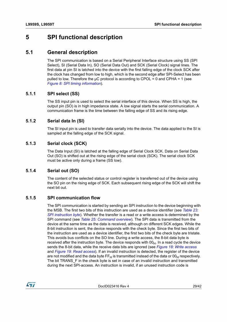
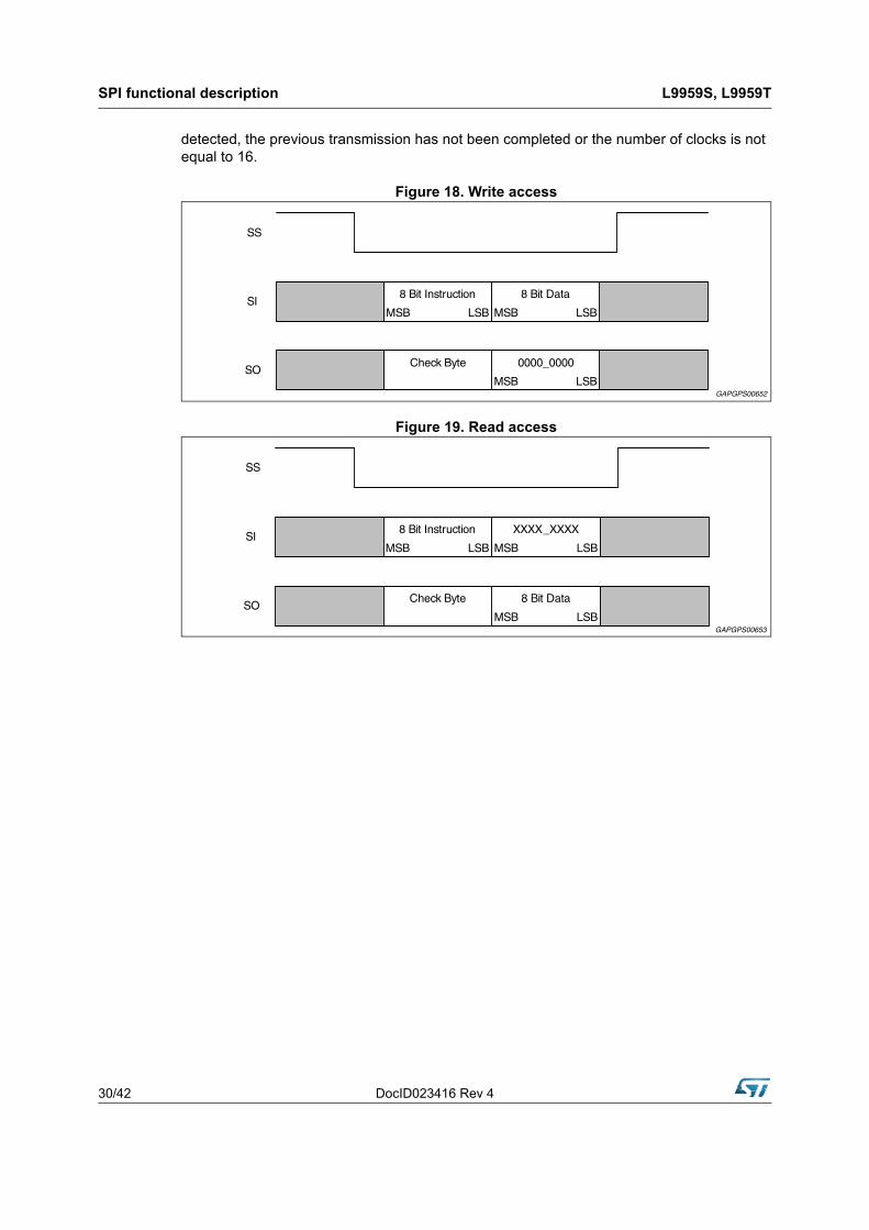
The SPI communication is started by sending an SPI instruction to the device beginning with the MSB. The first two bits of this instruction are used as a device identifier (see Table 23: SPI instruction byte). Whether the transfer is a read or a write access is determined by the SPI command (see Table 25: Command overview). The SPI data is transmitted from the device at the same time as the data is received, although on different SCK edges. While the 8-bit instruction is sent, the device responds with the check byte. Since the first two bits of the instruction are used as a device identifier, the first two bits of the check byte are tristate. This avoids bus conflicts on the SO line. During a write access, the 8-bit data byte is received after the instruction byte. The device responds with 00H. In a read cycle the device sends the 8-bit data, while the receive data bits are ignored (see Figure 18: Write access and Figure 19: Read access). If an invalid instruction is detected, the register of the device are not modified and the data byte FFH is transmitted instead of the data or 00H respectively. The bit TRANS_F in the check byte is set in case of an invalid instruction and transmitted during the next SPI-access. An instruction is invalid, if an unused instruction code is
SPI functional description L9959S, L9959T
30/42 DocID023416 Rev 4
detected, the previous transmission has not been completed or the number of clocks is not equal to 16.
Figure 18. Write access
Figure 19. Read access
DocID023416 Rev 4 31/42
L9959S, L9959T SPI functional description
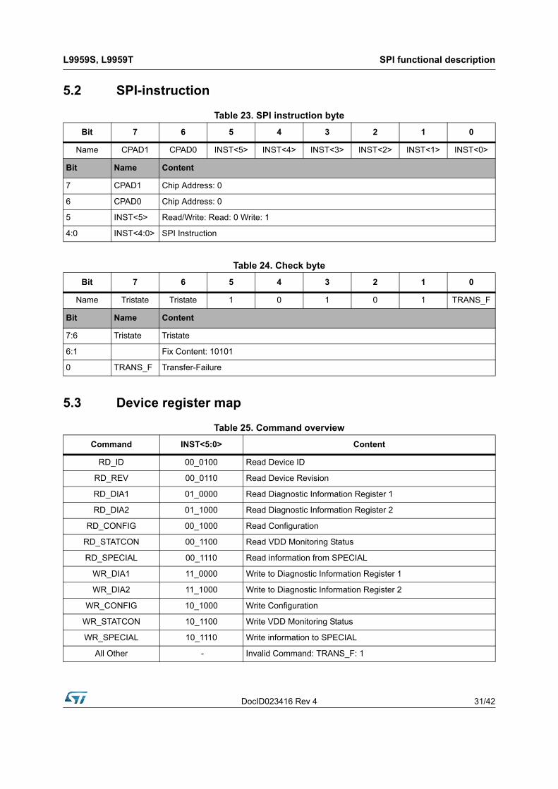
5.2 SPI-instruction
5.3 Device register map
Table 23. SPI instruction byte
Bit 7 6 5 4 3 2 1 0
Name CPAD1 CPAD0 INST<5> INST<4> INST<3> INST<2> INST<1> INST<0>
Bit Name Content
7 CPAD1 Chip Address: 0
6 CPAD0 Chip Address: 0
5 INST<5> Read/Write: Read: 0 Write: 1
4:0 INST<4:0> SPI Instruction
Table 24. Check byte
Bit 7 6 5 4 3 2 1 0
Name Tristate Tristate 1 0 1 0 1 TRANS_F
Bit Name Content
7:6 Tristate Tristate
6:1 Fix Content: 10101
0 TRANS_F Transfer-Failure
Table 25. Command overview
Command INST<5:0> Content
RD_ID 00_0100 Read Device ID
RD_REV 00_0110 Read Device Revision
RD_DIA1 01_0000 Read Diagnostic Information Register 1
RD_DIA2 01_1000 Read Diagnostic Information Register 2
RD_CONFIG 00_1000 Read Configuration
RD_STATCON 00_1100 Read VDD Monitoring Status
RD_SPECIAL 00_1110 Read information from SPECIAL
WR_DIA1 11_0000 Write to Diagnostic Information Register 1
WR_DIA2 11_1000 Write to Diagnostic Information Register 2
WR_CONFIG 10_1000 Write Configuration
WR_STATCON 10_1100 Write VDD Monitoring Status
WR_SPECIAL 10_1110 Write information to SPECIAL
All Other - Invalid Command: TRANS_F: 1
SPI functional description L9959S, L9959T
32/42 DocID023416 Rev 4
5.4 SPI - control and status registers
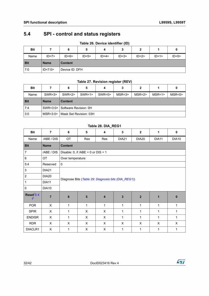
Table 26. Device identifier (ID)
Bit 7 6 5 4 3 2 1 0
Name ID<7> ID<6> ID<5> ID<4> ID<3> ID<2> ID<1> ID<0>
Bit Name Content
7:0 ID<7:0> Device ID: DFH
Table 27. Revision register (REV)
Bit 7 6 5 4 3 2 1 0
Name SWR<3> SWR<2> SWR<1> SWR<0> MSR<3> MSR<2> MSR<1> MSR<0>
Bit Name Content
7:4 SWR<3:0> Software Revision: 0H
3:0 MSR<3:0> Mask Set Revision: 03H
Table 28. DIA_REG1
Bit 7 6 5 4 3 2 1 0
Name /ABE / DIS OT Res Res DIA21 DIA20 DIA11 DIA10
Bit Name Content
7 /ABE / DIS Disable: 0, if /ABE = 0 or DIS = 1
6 OT Over temperature
5:4 Reserved 0
3 DIA21
Diagnose Bits (Table 29: Diagnosis bits (DIA_REG1)) 2 DIA20
1 DIA11
0 DIA10
Reset(5.4.1) 7 6 5 4 3 2 1 0
POR X 1 1 1 1 1 1 1
SPIR X 1 X X 1 1 1 1
ENDISR X 1 X X 1 1 1 1
RDR X X X X X X X X
DIACLR1 X 1 X X 1 1 1 1
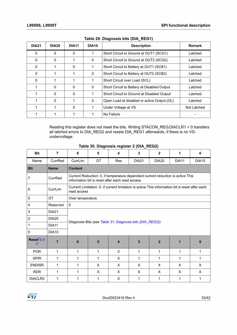
DocID023416 Rev 4 33/42
L9959S, L9959T SPI functional description
Reading this register does not reset the bits. Writing STACON_REG.DIACLR1 = 0 transfers all latched errors to DIA_REG2 and resets DIA_REG1 afterwards, if there is no VS-undervoltage.
Table 29. Diagnosis bits (DIA_REG1)
DIA21 DIA20 DIA11 DIA10 Description Remark
0 0 0 1 Short Circuit to Ground at OUT1 (SCG1) Latched
0 0 1 0 Short Circuit to Ground at OUT2 (SCG2) Latched
0 1 0 1 Short Circuit to Battery at OUT1 (SCB1) Latched
0 1 1 0 Short Circuit to Battery at OUT2 (SCB2) Latched
0 1 1 1 Short Circuit over Load (SCL) Latched
1 0 0 0 Short Circuit to Battery at Disabled Output Latched
1 0 0 1 Short Circuit to Ground at Disabled Output Latched
1 0 1 0 Open Load at disabled or active Output (OL) Latched
1 1 0 1 Under Voltage at VS Not Latched
1 1 1 1 No Failure -
Table 30. Diagnosis register 2 (DIA_REG2)
Bit 7 6 5 4 3 2 1 0
Name CurrRed CurrLim OT Res DIA21 DIA20 DIA11 DIA10
Bit Name Content
7 CurrRed Current Reduction: 0, if temperature dependent current reduction is active This information bit is reset after each read access
6 CurrLim Current Limitation: 0, if current limitation is active This information bit is reset after each read access
5 OT Over temperature
4 Reserved 0
3 DIA21
Diagnosis Bits (see Table 31: Diagnosis bits (DIA_REG2)) 2 DIA20
1 DIA11
0 DIA10
Reset(5.4.1) 7 6 5 4 3 2 1 0
POR 1 1 1 0 1 1 1 1
SPIR 1 1 1 X 1 1 1 1
ENDISR 1 1 X X X X X X
RDR 1 1 X X X X X X
DIACLR2 1 1 1 X 1 1 1 1
SPI functional description L9959S, L9959T
34/42 DocID023416 Rev 4
Only the bit ‘RESET’ in this register can be written, all other bits are ‘read-only’
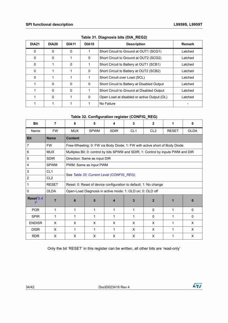
Table 31. Diagnosis bits (DIA_REG2)
DIA21 DIA20 DIA11 DIA10 Description Remark
0 0 0 1 Short Circuit to Ground at OUT1 (SCG1) Latched
0 0 1 0 Short Circuit to Ground at OUT2 (SCG2) Latched
0 1 0 1 Short Circuit to Battery at OUT1 (SCB1) Latched
0 1 1 0 Short Circuit to Battery at OUT2 (SCB2) Latched
0 1 1 1 Short Circuit over Load (SCL) Latched
1 0 0 0 Short Circuit to Battery at Disabled Output Latched
1 0 0 1 Short Circuit to Ground at Disabled Output Latched
1 0 1 0 Open Load at disabled or active Output (OL) Latched
1 1 1 1 No Failure -
Table 32. Configuration register (CONFIG_REG)
Bit 7 6 5 4 3 2 1 0
Name FW MUX SPWM SDIR CL1 CL2 RESET OLDA
Bit Name Content
7 FW Free-Wheeling: 0: FW via Body Diode; 1: FW with active short of Body Diode
6 MUX Multiplex Bit: 0: control by bits SPWM and SDIR; 1: Control by inputs PWM and DIR
5 SDIR Direction: Same as input DIR
4 SPWM PWM: Same as input PWM
3 CL1 See Table 33: Current Level (CONFIG_REG).
2 CL2
1 RESET Reset: 0: Reset of device configuration to default; 1: No change
0 OLDA Open-Load Diagnosis in active mode: 1: OLD on; 0: OLD off
Reset(5.4.1) 7 6 5 4 3 2 1 0
POR 1 1 1 1 1 0 1 0
SPIR 1 1 1 1 1 0 1 0
ENDISR X X X X X X 1 X
DISR X 1 1 1 X X 1 X
RDR X X X X X X 1 X
DocID023416 Rev 4 35/42
L9959S, L9959T SPI functional description
Only the bits ‘CONFIG’ and ‘DIACLR’ in this register can be written, all other bits are ‘read-only’
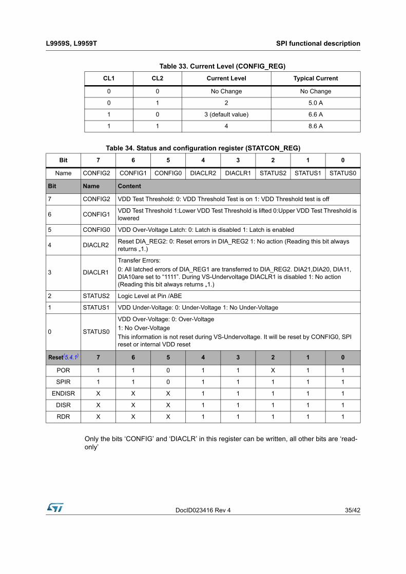
Table 33. Current Level (CONFIG_REG)
CL1 CL2 Current Level Typical Current
0 0 No Change No Change
0 1 2 5.0 A
1 0 3 (default value) 6.6 A
1 1 4 8.6 A
Table 34. Status and configuration register (STATCON_REG)
Bit 7 6 5 4 3 2 1 0
Name CONFIG2 CONFIG1 CONFIG0 DIACLR2 DIACLR1 STATUS2 STATUS1 STATUS0
Bit Name Content
7 CONFIG2 VDD Test Threshold: 0: VDD Threshold Test is on 1: VDD Threshold test is off
6 CONFIG1 VDD Test Threshold 1:Lower VDD Test Threshold is lifted 0:Upper VDD Test Threshold is lowered
5 CONFIG0 VDD Over-Voltage Latch: 0: Latch is disabled 1: Latch is enabled
4 DIACLR2 Reset DIA_REG2: 0: Reset errors in DIA_REG2 1: No action (Reading this bit always returns „1.)
3 DIACLR1
Transfer Errors:
0: All latched errors of DIA_REG1 are transferred to DIA_REG2. DIA21,DIA20, DIA11, DIA10are set to “1111”. During VS-Undervoltage DIACLR1 is disabled 1: No action (Reading this bit always returns „1.)
2 STATUS2 Logic Level at Pin /ABE
1 STATUS1 VDD Under-Voltage: 0: Under-Voltage 1: No Under-Voltage
0 STATUS0
VDD Over-Voltage: 0: Over-Voltage
1: No Over-Voltage
This information is not reset during VS-Undervoltage. It will be reset by CONFIG0, SPI reset or internal VDD reset
Reset(5.4.1) 7 6 5 4 3 2 1 0
POR 1 1 0 1 1 X 1 1
SPIR 1 1 0 1 1 1 1 1
ENDISR X X X 1 1 1 1 1
DISR X X X 1 1 1 1 1
RDR X X X 1 1 1 1 1
SPI functional description L9959S, L9959T
36/42 DocID023416 Rev 4
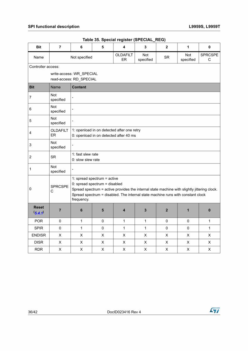
Table 35. Special register (SPECIAL_REG)
Bit 7 6 5 4 3 2 1 0
Name Not specifiedOLDAFILT
ERNot
specified SR
Not specified
SPRCSPEC
Controller access:
write-access: WR_SPECIAL
read-access: RD_SPECIAL
Bit Name Content
7 Not specified
-
6 Not specified
-
5 Not specified
-
4 OLDAFILTER
1: openload in on detected after one retry
0: openload in on detected after 40 ms
3 Not specified
-
2 SR 1: fast slew rate
0: slow slew rate
1 Not specified
-
0 SPRCSPEC
1: spread spectrum = active
0: spread spectrum = disabled
Spread spectrum = active provides the internal state machine with slightly jittering clock.
Spread spectrum = disabled. The internal state machine runs with constant clock frequency.
Reset(5.4.1) 7 6 5 4 3 2 1 0
POR 0 1 0 1 1 0 0 1
SPIR 0 1 0 1 1 0 0 1
ENDISR X X X X X X X X
DISR X X X X X X X X
RDR X X X X X X X X
DocID023416 Rev 4 37/42
L9959S, L9959T SPI functional description
5.4.1 Reset sources
POR: Reset due to a VDD power up on VDD (Power-Up Reset)
ENDISR: Reset caused by an enable or disable of the power stages (DIS or /ABE edge triggered) (Enable-/Disable Reset)
DISR: Reset caused by disabling the power stages (DIS or /ABE level triggered) (Disable power stage reset)
5.4.2 Configuration registers reset sources
POR: Reset due to a VDD power up on VDD (Power-Up Reset)
SPIR: Reset by setting bit RESET in the configuration register (CONFIG_REG) (SPIReset)
RDIR: Reset caused by a read access to the corresponding register (Read Register)
DIACLR1: Reset by setting bit DIACLR1 in the Status and Configuration Register STATCON (Diagnosis Reset 1)
DIACLR2: Reset by setting bit DIACLR2 in the Status and Configuration Register STATCON (Diagnosis Reset 2)
Application circuit L9959S, L9959T
38/42 DocID023416 Rev 4
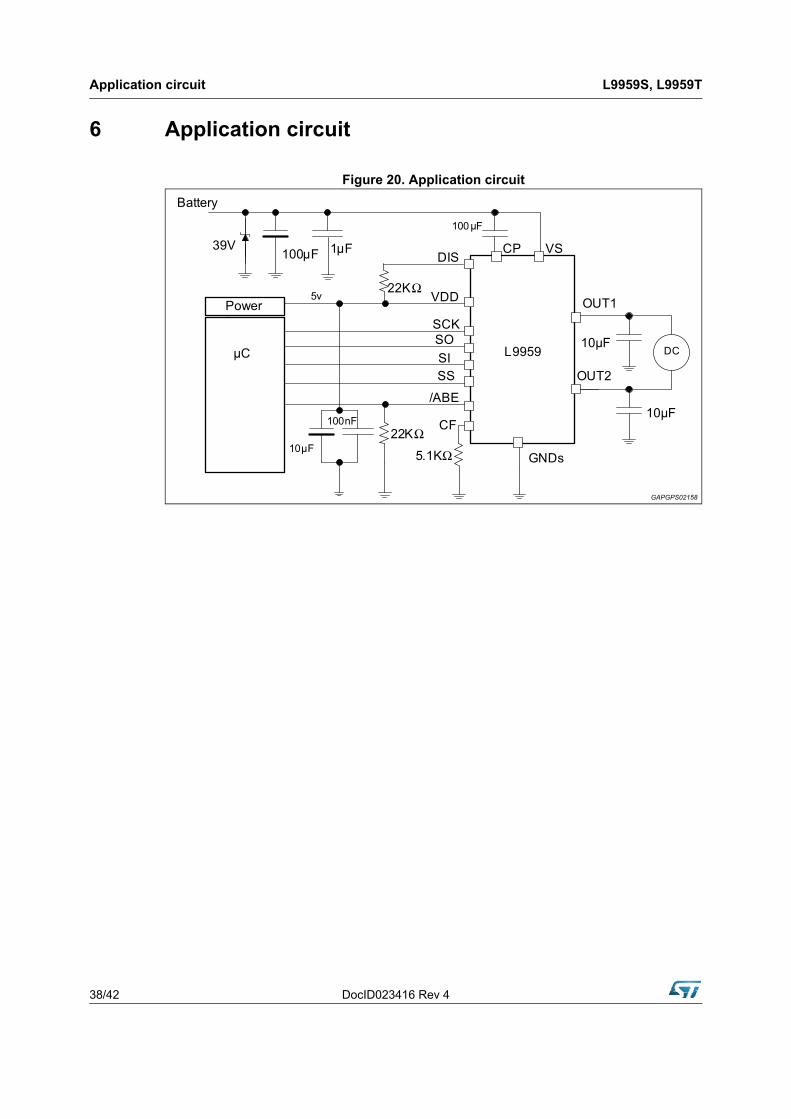
6 Application circuit
Figure 20. Application circuit
DocID023416 Rev 4 39/42
L9959S, L9959T Package information
7 Package information
In order to meet environmental requirements, ST offers these devices in different grades of ECOPACK® packages, depending on their level of environmental compliance. ECOPACK® specifications, grade definitions and product status are available at: www.st.com.
ECOPACK® is an ST trademark.
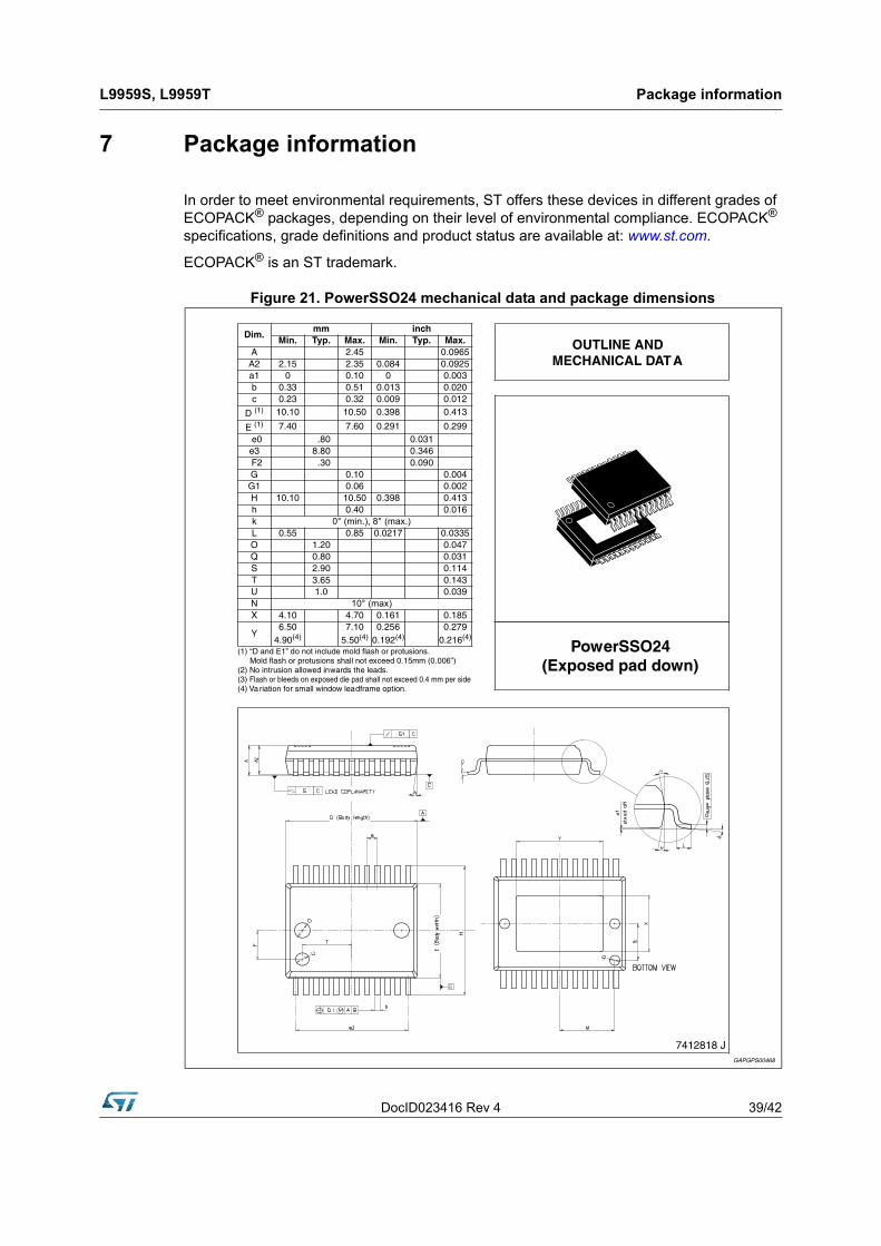
Figure 21. PowerSSO24 mechanical data and package dimensions
Package information L9959S, L9959T
40/42 DocID023416 Rev 4
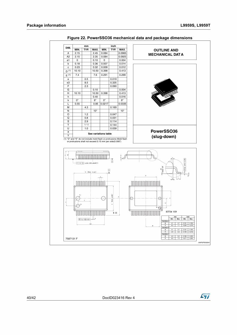
Figure 22. PowerSSO36 mechanical data and package dimensions
DocID023416 Rev 4 41/42
L9959S, L9959T Revision history
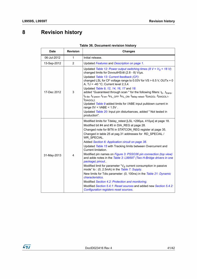
8 Revision history
Table 36. Document revision history
Date Revision Changes
06-Jul-2012 1 Initial release.
13-Sep-2012 2 Updated Features and Description on page 1.
17-Dec 2012 3
Updated Table 12: Power output switching times (8 V < VS < 18 V):changed limits for DovoutHS/dt (2.8 - 8) V/µs.
Updated Table 13: Current feedback (CF):changed LSL for CF voltage range to 0.03V for VS > 6.5 V, OUTx = 0 A, TJ = -40 °C; Current level 2,3,4.
Updated Table 9, 12, 14, 16, 17 and 18:added “Guaranteed through scan " for the following filters: tb , ttrans, td dis, td pwon, td en, tFIL_OFF, tFIL_ON, tdelay retest, tDIAGOL, tDIAGOL1, tDIAGOL2.
Updated Table 9 added limits for //ABE input pulldown current in range 0V < VABE < 1.5V .
Updated Table 20: Input pin disturbances, added " Not tested in production".
31-May-2013 4
Modified limits for Tdelay_retest [LSL =290µs, 410µs] at page 18.
Modified bit #4 and #5 in DIA_REG at page 28.
Changed note for BIT6 in STATCON_REG register at page 35.
Changed in table 25 at pag.31 addresses for RD_SPECIAL / WR_SPECIAL.
Added Section 6: Application circuit on page 38.
Updated Table 15 with Tracking limits between Overcurrent and Current limitation.
Modified pin names on Figure 3: PSSO36 pin connection (top view) and adde notes in the Table 3: L9959T (Two H-Bridge drivers in one package) pinout..
Modified limit for parameter “VS current consumption in passive mode” to : (0, 2.5mA) in the Table 7: Supply.
New limits for Tdis parameter: (0, 100ns) in the Table 21: Dynamic characteristics.
Modified Section 4.2: Protection and monitoring.
Modified Section 5.4.1: Reset sources and added new Section 5.4.2: Configuration registers reset sources.
L9959S, L9959T
42/42 DocID023416 Rev 4
Please Read Carefully:
Information in this document is provided solely in connection with ST products. STMicroelectronics NV and its subsidiaries (“ST”) reserve theright to make changes, corrections, modifications or improvements, to this document, and the products and services described herein at anytime, without notice.
All ST products are sold pursuant to ST’s terms and conditions of sale.
Purchasers are solely responsible for the choice, selection and use of the ST products and services described herein, and ST assumes noliability whatsoever relating to the choice, selection or use of the ST products and services described herein.
No license, express or implied, by estoppel or otherwise, to any intellectual property rights is granted under this document. If any part of thisdocument refers to any third party products or services it shall not be deemed a license grant by ST for the use of such third party productsor services, or any intellectual property contained therein or considered as a warranty covering the use in any manner whatsoever of suchthird party products or services or any intellectual property contained therein.
UNLESS OTHERWISE SET FORTH IN ST’S TERMS AND CONDITIONS OF SALE ST DISCLAIMS ANY EXPRESS OR IMPLIEDWARRANTY WITH RESPECT TO THE USE AND/OR SALE OF ST PRODUCTS INCLUDING WITHOUT LIMITATION IMPLIEDWARRANTIES OF MERCHANTABILITY, FITNESS FOR A PARTICULAR PURPOSE (AND THEIR EQUIVALENTS UNDER THE LAWSOF ANY JURISDICTION), OR INFRINGEMENT OF ANY PATENT, COPYRIGHT OR OTHER INTELLECTUAL PROPERTY RIGHT.
ST PRODUCTS ARE NOT AUTHORIZED FOR USE IN WEAPONS. NOR ARE ST PRODUCTS DESIGNED OR AUTHORIZED FOR USEIN: (A) SAFETY CRITICAL APPLICATIONS SUCH AS LIFE SUPPORTING, ACTIVE IMPLANTED DEVICES OR SYSTEMS WITHPRODUCT FUNCTIONAL SAFETY REQUIREMENTS; (B) AERONAUTIC APPLICATIONS; (C) AUTOMOTIVE APPLICATIONS ORENVIRONMENTS, AND/OR (D) AEROSPACE APPLICATIONS OR ENVIRONMENTS. WHERE ST PRODUCTS ARE NOT DESIGNEDFOR SUCH USE, THE PURCHASER SHALL USE PRODUCTS AT PURCHASER’S SOLE RISK, EVEN IF ST HAS BEEN INFORMED INWRITING OF SUCH USAGE, UNLESS A PRODUCT IS EXPRESSLY DESIGNATED BY ST AS BEING INTENDED FOR “AUTOMOTIVE,AUTOMOTIVE SAFETY OR MEDICAL” INDUSTRY DOMAINS ACCORDING TO ST PRODUCT DESIGN SPECIFICATIONS.PRODUCTS FORMALLY ESCC, QML OR JAN QUALIFIED ARE DEEMED SUITABLE FOR USE IN AEROSPACE BY THECORRESPONDING GOVERNMENTAL AGENCY.
Resale of ST products with provisions different from the statements and/or technical features set forth in this document shall immediately voidany warranty granted by ST for the ST product or service described herein and shall not create or extend in any manner whatsoever, anyliability of ST.
ST and the ST logo are trademarks or registered trademarks of ST in various countries.Information in this document supersedes and replaces all information previously supplied.
The ST logo is a registered trademark of STMicroelectronics. All other names are the property of their respective owners.
© 2013 STMicroelectronics - All rights reserved
STMicroelectronics group of companies
Australia - Belgium - Brazil - Canada - China - Czech Republic - Finland - France - Germany - Hong Kong - India - Israel - Italy - Japan - Malaysia - Malta - Morocco - Philippines - Singapore - Spain - Sweden - Switzerland - United Kingdom - United States of America
www.st.com