Embed Size (px)
Citation preview

Semi Networking Day – Milano 20 Settembre 2012 1
Since 1972 Since 1972 PoweringPowering the Futurethe Future
C o
r p
o r
a t
e
P
r o
f i
l e
C o
r p
o r
a t
e
P
r o
f i
l e
C o
r p
o r
a t
e
P
r o
f i
l e
Semi Networking Day – Milano 20 Settembre 2012

Semi Networking Day – Milano 20 Settembre 2012 2
• LPE
Vision : to help develop Energy Efficient Solutions
Mission : To be the market & technology leader in epitaxial technologies for Smart Power Management and Sensor Solutions
Vision & Mission Vision & Mission
C o
r p
o r
a t
e
P
r o
f i
l e
C o
r p
o r
a t
e
P
r o
f i
l e
C o
r p
o r
a t
e
P
r o
f i
l e

Semi Networking Day – Milano 20 Settembre 2012 3
• LPE is a worldwide specialist in epitaxial technologies
for Power Management , Power Saving and Sensor
applications
• Our clear mission is to provide our Customers with
leading edge equipment and process solutions for
advanced and traditional discrete devices , new
generation sensors , improving Customers' process
performance , lowering environmental impact and
lowering manufacturing costs
Our strengthsOur strengths
C o
r p
o r
a t
e
P
r o
f i
l e
C o
r p
o r
a t
e
P
r o
f i
l e
C o
r p
o r
a t
e
P
r o
f i
l e

Semi Networking Day – Milano 20 Settembre 2012 4
• We provide epitaxy reactors for silicon and silicon carbide
built around LPE proprietary reaction chambers and core
technology IP
• Our reactors are particularly suited for thick and very
thick epi layers on substrates and patterned wafers ,
maintaining quality standards typical of thin epi layers
• Our Customers are both devices makers and epi houses ,
operating worldwide
Our strengthsOur strengths
C o
r p
o r
a t
e
P
r o
f i
l e
C o
r p
o r
a t
e
P
r o
f i
l e
C o
r p
o r
a t
e
P
r o
f i
l e

Semi Networking Day – Milano 20 Settembre 2012 5
Historical factsHistorical facts
1972.1972.
PretiPreti Engineering ( now LPE ) designs and manufactures the first Engineering ( now LPE ) designs and manufactures the first
silicon Epitaxial Reactor in Europe.silicon Epitaxial Reactor in Europe.
Almost 40 years later LPE reactors are still the preferred toolAlmost 40 years later LPE reactors are still the preferred tools to s to
grow EPI layers for discrete and power applications.grow EPI layers for discrete and power applications.
Over 400 reaction chambers are in operation in more than 30 Over 400 reaction chambers are in operation in more than 30
leading semiconductor companies. leading semiconductor companies.
LPE has become a global leader by offering the most advanced LPE has become a global leader by offering the most advanced
equipment for Epitaxial Deposition.equipment for Epitaxial Deposition.
C o
r p
o r
a t
e
P
r o
f i
l e
C o
r p
o r
a t
e
P
r o
f i
l e
C o
r p
o r
a t
e
P
r o
f i
l e

Semi Networking Day – Milano 20 Settembre 2012 6
Worldwide organizationWorldwide organization
SUBSIDIARIES
ETC Italy
LPE Shanghai
Headquarters Milan, ItalyHeadquarters Milan, Italy
AGENTS
Japan
USA
Taiwan
South Korea
Czech
Republic
C o
r p
o r
a t
e
P
r o
f i
l e
C o
r p
o r
a t
e
P
r o
f i
l e
C o
r p
o r
a t
e
P
r o
f i
l e

Semi Networking Day – Milano 20 Settembre 2012 7
EuroEuro USD USD avgavg
20042004 11.1 ME11.1 ME 13.8 M$13.8 M$
20052005 17.9 ME17.9 ME 22.2 M$22.2 M$
20062006 19.8 19.8 MEME 24.8 M$24.8 M$
20072007 16.6 16.6 MEME 22.7 M$22.7 M$
20082008 13.1 13.1 MEME 19.2 M$19.2 M$
20092009 5.4 5.4 MEME 7.6 M$7.6 M$
2010 2010 19.4 ME 19.4 ME 27.0 M$27.0 M$
20112011 43.0 ME43.0 ME 60.0 M$60.0 M$
20122012 1717--25 ME budget 25 ME budget
RevenueRevenue
C o
r p
o r
a t
e
P
r o
f i
l e
C o
r p
o r
a t
e
P
r o
f i
l e
C o
r p
o r
a t
e
P
r o
f i
l e

Semi Networking Day – Milano 20 Settembre 2012 8
PE 3061 D
PE2061 S
Installed Base: >140Located in all world regions since 1992
Silicon Epitaxy O
u r
P
r o
d u
c t
s
O u
r
P r
o d
u c
t s
O
u r
P
r o
d u
c t
s
Silicon Equipment Product LineSilicon Equipment Product Line
Installed Base: > 130 Located in all world regions since 2000

Semi Networking Day – Milano 20 Settembre 2012 9
InventaPro (CVD)Installed Base:
3 in Japan
3 in Europe
ACiS
SiC Epitaxy SiC Bulk (R&D)O
u r
P
r o
d u
c t
s
O u
r
P r
o d
u c
t s
O
u r
P
r o
d u
c t
s
Subli100 (PVT)
SiC Equipment Product Line SiC Equipment Product Line (since 2008)(since 2008)

Semi Networking Day – Milano 20 Settembre 2012 10
Silicon and Silicon CarbideSilicon and Silicon Carbide
CustomersCustomers
C u
s t
o m
e r
sC
u s
t o
m e
r s
C u
s t
o m
e r
s

Semi Networking Day – Milano 20 Settembre 2012 11
EuropeEurope
Semi Networking Day – Milano 20 Settembre 2012 12
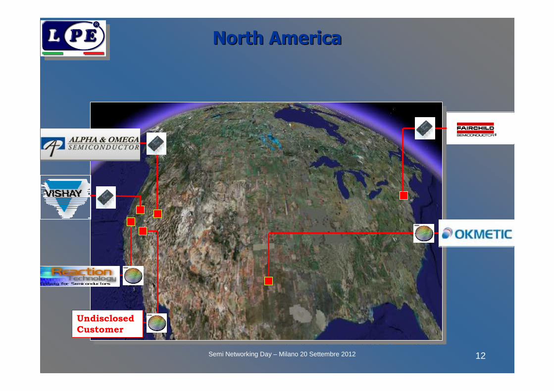
North AmericaNorth America
Undisclosed
Customer

Semi Networking Day – Milano 20 Settembre 2012 13
Korea & JapanKorea & Japan
Undisclosed
Customer

Semi Networking Day – Milano 20 Settembre 2012 14
Yanhe Factory
China & TaiwanChina & Taiwan
Fushun

Semi Networking Day – Milano 20 Settembre 2012 15
…….and.and SingaporeSingapore

Semi Networking Day – Milano 20 Settembre 2012 16
LPE Group innovation LPE Group innovation
L P
E
G r
o u
p
I n
n o
v a
t i
o n
L P
E
G r
o u
p
I n
n o
v a
t i
o n
L P
E
G r
o u
p
I n
n o
v a
t i
o n

Semi Networking Day – Milano 20 Settembre 2012 17
Extend the application of LPE know-how to the following domains :
• Power Management / Power Saving
- Silicon epitaxy
- SiC homo & hetero epitaxy
- Other WBG materials
LPE Group strategyLPE Group strategy
L P
E
G r
o u
p
I n
n o
v a
t i
o n
L P
E
G r
o u
p
I n
n o
v a
t i
o n
L P
E
G r
o u
p
I n
n o
v a
t i
o n

Semi Networking Day – Milano 20 Settembre 2012 18
LPE Mission :
• Equipment for epitaxy (Si and SiC)
• Design
• Manufacturing
• Sales
ETC Mission :
• Epitaxial growth processes
• Epitaxial wafers supply
LPE Group strategyLPE Group strategy
L P
E
G r
o u
p
I n
n o
v a
t i
o n
L P
E
G r
o u
p
I n
n o
v a
t i
o n
L P
E
G r
o u
p
I n
n o
v a
t i
o n

Semi Networking Day – Milano 20 Settembre 2012 19
Since 1972 Since 1972 PoweringPowering the Futurethe Future
ETCETC
EEpitaxial pitaxial TTechnology echnology CCenterenter
C o
r p
o r
a t
e
P
r o
f i
l e
C o
r p
o r
a t
e
P
r o
f i
l e
C o
r p
o r
a t
e
P
r o
f i
l e

Semi Networking Day – Milano 20 Settembre 2012 20
• Epitaxy experts SILICON and SiC
• Significant effort and investment made to develop SiC
epi and know-how on substrate growth technology
• SiCiLab R&D lab with CNR support & staff inside ETC
• ENIAC European projects:
• 150 mm SiC epi
• 300mm Silicon
ET
CE
TC
ET
C
ETC Key FactsETC Key Facts

Semi Networking Day – Milano 20 Settembre 2012 21
ETC ETC EpitaxyEpitaxy ServiceService
ET
CE
TC
ET
C• ETC offers a complete range of SiC Epitaxy specifications
on wafers from 2” to 200mm diameter
• 4H SiC blanket homoepitaxial layer, with a wide range of
thicknesses and doping concentrations for both n and p-type
doping
• A unique multistep high-growth-rate (HGR) epitaxial process
for complex p-n junctions structures
• A patented Virtual Substrate process for high thickness
(>100µm) and low doping (<5x10¹³at/cm3) for sensors
applications
• 3C SiC heteroepitaxy on silicon on any diameter up to
200mm and most silicon orientations for MEMS application
Semi Networking Day – Milano 20 Settembre 2012 22
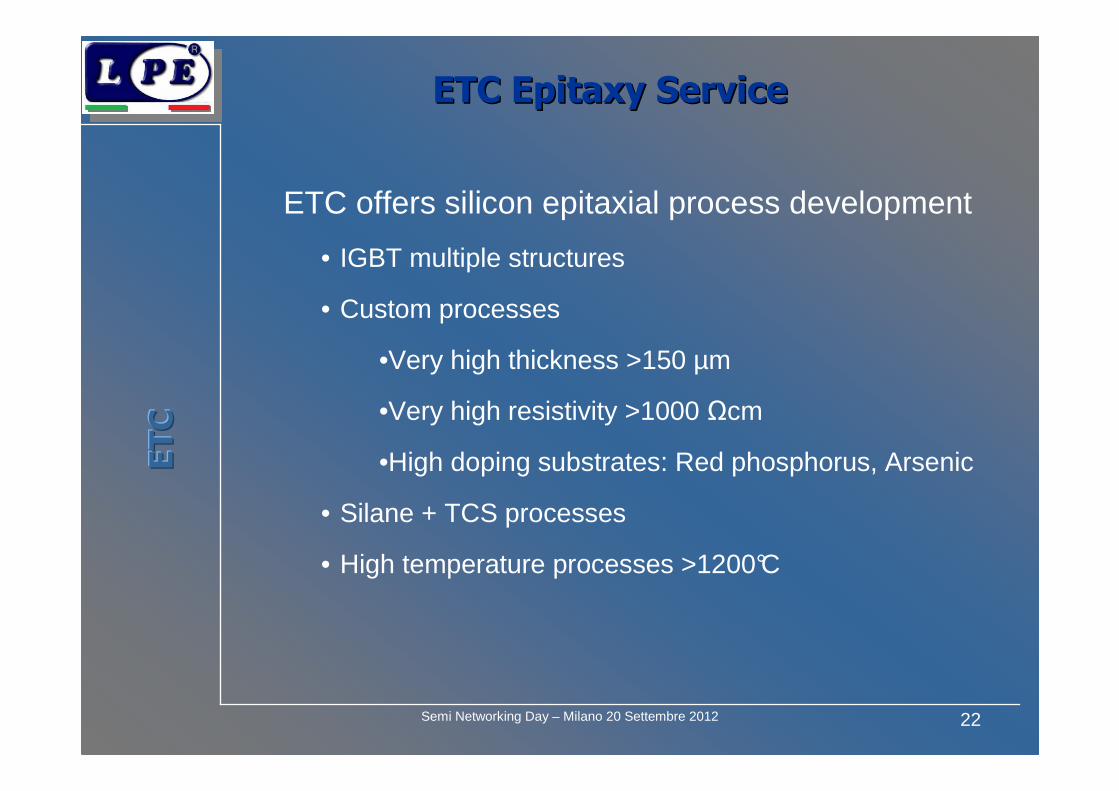
ETC ETC EpitaxyEpitaxy ServiceService
ET
CE
TC
ET
C
ETC offers silicon epitaxial process development
• IGBT multiple structures
• Custom processes
•Very high thickness >150 µm
•Very high resistivity >1000 Ωcm
•High doping substrates: Red phosphorus, Arsenic
• Silane + TCS processes
• High temperature processes >1200°C

Semi Networking Day – Milano 20 Settembre 2012 23
ETC ETC EpitaxyEpitaxy ServiceService
ET
CE
TC
ET
C
• Internal characterization capability
• Layer thickness mapping: FTIR QS2200
• Carrier concentration mapping and in-depth profiling:
CV Mercury probe SSM 495
• Nikon automatic inspection for defects mapping (bright
field, dark field, DIC, confocal)

Semi Networking Day – Milano 20 Settembre 2012 24
ETC ETC EpitaxyEpitaxy ServiceService
ET
CE
TC
ET
C• In the SiCilab (www.sicilab.it)
• X-Ray diffraction
• Polar figures
• Rocking curve maps
• Stress measurements
• Optical characterization
• µ-Raman map
• µ-Photoluminescence map
• time-resolved photoluminescence
• Electrical characterization
• I-V and C-V by device test patterns
• DLTS
• Stress characterization by test structures (3C-SiC)

Semi Networking Day – Milano 20 Settembre 2012 25
ETC ETC EpitaxyEpitaxy ServiceService
SiCSiC MEMS test structuresMEMS test structuresE
TC
ET
CE
TC
microstructures:
V1 V2
Beams (Cantilevers)
“Bicycle Wheels”
Planar rotatingsensors
SpiralsTensileStress
compressive Stress

Semi Networking Day – Milano 20 Settembre 2012 26
ETC ETC SiCSiC
ET
CE
TC
ET
C

Semi Networking Day – Milano 20 Settembre 2012 27
ETC SiliconETC Silicon
ET
CE
TC
ET
C

Semi Networking Day – Milano 20 Settembre 2012 28
谢谢谢谢谢谢谢谢
thank youdanke
有難うございました。有難うございました。有難うございました。有難うございました。
obrigado
kiitos
teşekkürler
gracias
спасибо
dzięki
takk
спасибі
ขอบคณ
nhờ
tack
shukrani
hvalavďaka
хвала
mul ţumiri
ر
grazzi
terima kasih
благодарамačiū
paldies
감사감사감사감사
raibh maith agat
köszönöm
धयवाद
תודה
ευχαριστίες
grazas
mercisalamat
tänanbedankt tak
díky
hvala
gràcies
благодаря
дзякуй را
faleminderit
dankie
მადლობამადლობამადლობამადლობა
GrazieGrazie