Embed Size (px)
Citation preview

SILICON LENSES FOR BAND 2+3TONY MROCZKOWSKI
Or What I learned about Lenses from the CCAT and CMB communities
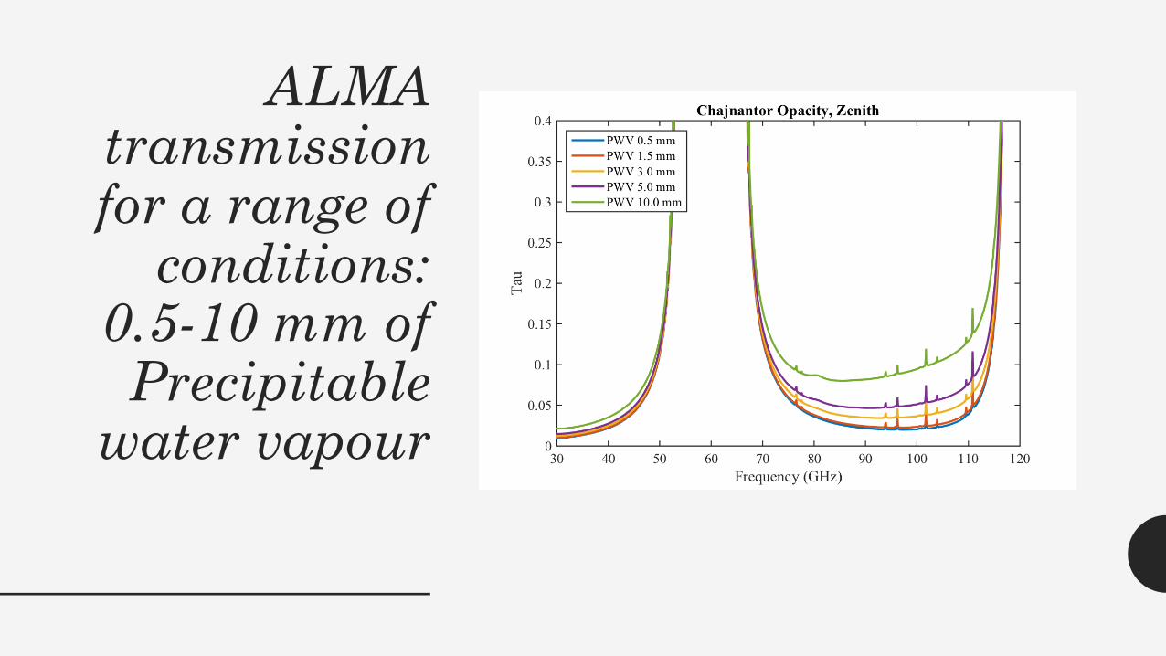
ALMA transmission for a range of
conditions: 0.5-10 mm of Precipitable
water vapour

Corresponding noise temperature
of the sky
remains low (<20 K) for a broad
range of conditions
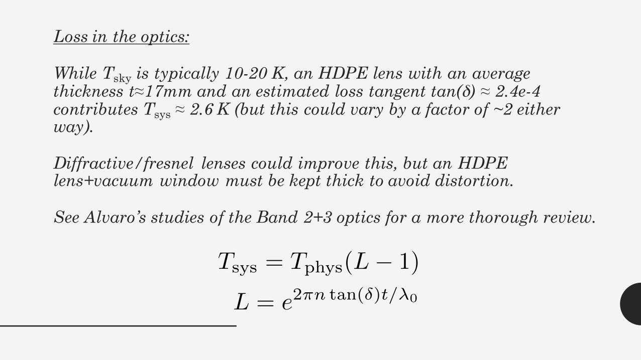
Loss in the optics:
While Tsky is typically 10-20 K, an HDPE lens with an average thickness t≈17mm and an estimated loss tangent tan(δ) ≈ 2.4e-4 contributes Tsys ≈ 2.6 K (but this could vary by a factor of ~2 either way).
Diffractive/fresnel lenses could improve this, but an HDPE lens+vacuum window must be kept thick to avoid distortion.
See Alvaro’s studies of the Band 2+3 optics for a more thorough review.
Tsys = Tphys(L� 1)
L = e2⇡n tan(�)t/�0

Silicon offers an alternative that can be thinner and less
lossy.
Plotted here is the loss tangents for 2 types high-
resistivity Silicon (from Lamb 1996, compiled from Parshin
1995). Black + are measurements, lines are
linear interp/extrapolations.
These results are already 20 years old.
Frequency (GHz)
50 100 150 200 250 300L
oss
Tan
gen
t ×
10
4
0.1
0.2
0.3
0.4
0.5
0.6
Loss Tangent, extrap. from Lamb 1996 / Parshin 1995 values
HP SieHR Si

“At 35 GHz the loss tangent is ~0.004 for a Si wafer having a bulk
resistivity of 1 kΩ cm.” from Topsil’s APPLICATION NOTE: HIGH RESISTIVITY(HiResTM)
SILICON FOR GHz & THz TECHNOLOGY
(http://www.topsil.com/media/123119/hires_application_note_v1.1_jan
uary2014.pdf).
Prediction: At resistivity > 10 kΩ-cm, the loss tangent should scale to < 0.4 x 10⁻⁴ at 35 GHz, and falls as
1/frequency.Frequency (GHz)
50 100 150 200 250 300L
oss
Tan
gen
t ×
10
4
0.1
0.2
0.3
0.4
0.5
0.6
Loss Tangent, extrap. from Lamb 1996 / Parshin 1995 values
HP SieHR Si

Corresponding noise temperature contribution
for 10 mm thick Si lens (with Parshin et al. 1995 /
Lamb 1996 silicon).
Silicon could also be made thinner (3-4 mm) as a
diffractive lens
Frequency (GHz)
70 80 90 100 110 120T
sys (
K)
0.7
0.75
0.8
0.85
0.9
0.95
1
1.05
1.1Noise Temperature Contribution of 10 mm thick 300 K lens
HP SieHR Si

Developments in recent years• Up to 70kΩ-cm ultrahigh purity float zone (FZ) silicon is widely available in up to 200 mm diameters (e.g.
from Topsil).
• The loss tangent scales inversely with resistivity, so we should be able to reduce the loss by a factor of 10 immediately from the Topsil 2014 measurements.
• Jeff McMahon (from Datta et al. 2013 ACTPol lens paper) has measured warm loss tangents of tan(δ)<8e-6 at 150 GHz. Scaling to Band 2+3, this will yield tan(δ)< 2e-5 (or Tsys<0.2 K).
• Silicon has a very high index of refraction (n=3.4), making it attractive for thin lenses with less extreme curvatures.
• Impedance matching over the wide bandwidths used to be more challenging, using multiple layers of plastics. Plastic coatings are lossy, can de-adhere from the lens surface, and we cannot choose the precise index/indices of refraction necessary.
• Thanks to recent work in the CMB community (and later, in CCAT development studies), wide bandwidth AR surfacing techniques have been realized (e.g. Datta et al. 2013 ACTPol lenses). This takes advantage of better machining (multi-axis milling and dicing saws) as well as advances in desktop computing for E&M simulations/optimizations.

Advanced AR techniques
(Datta+ 2013)Dicing saw approach to removing enough
volume at subwavelength scales to tune the impedance.
Grid geometry avoids birefringence in the index (unlike concentric grooves). Geometry shown on
right.
Nested grooves are optimized in HFSS to provide nearly an octave of bandwidth.
One can do even better with more layers.
Will scale easily to Band 2+3 , where features are larger
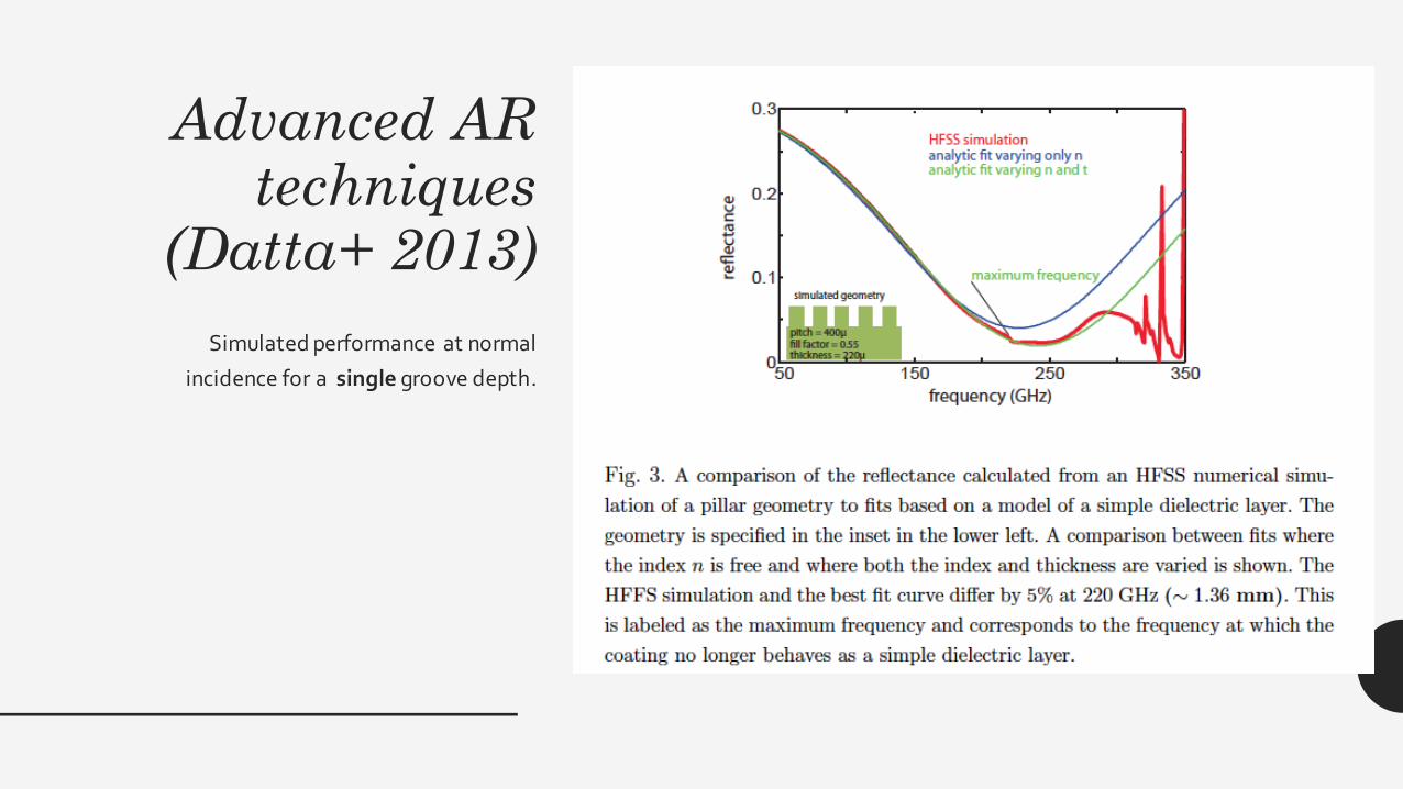
Advanced AR techniques
(Datta+ 2013)Simulated performance at normal
incidence for a single groove depth.

Advanced AR techniques
(Datta+ 2013)Simulated performance using 2 nested
groove depths.
Performs well even at 30 degrees
incidence.
Broadband AR is appealing for Bands 2+3
as well as any future wideband ALMA
receivers requiring lenses.

Datta et al. 2013
measurementsMeasured performance closely matches the
simulation

Effect of non-normal incidenceAt the edge of a Band 2+3 lens, the angle will be
7.5 degrees for a double-sided lens, or 15.1
degrees for a single sided lens.
Datta et al. 2013 found little impact on the AR
band and reflectivity due to non-normal
incidences at small angle (and even somewhat
acceptable performance for a 30 degree angle of
incidence).
Plots (from Datta+ 13) show simulations
including 1 and 2 sides, vs measurements
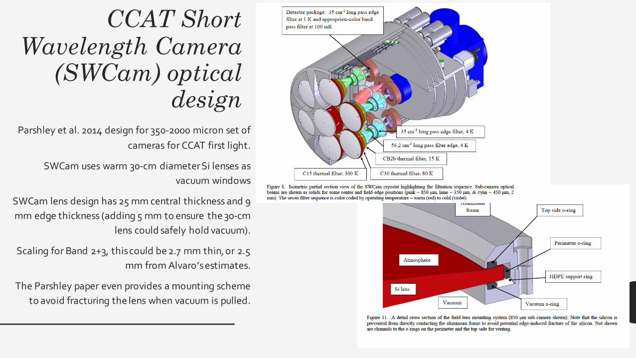
CCAT Short Wavelength Camera
(SWCam) optical design
Parshley et al. 2014 design for 350-2000 micron set of cameras for CCAT first light.
SWCam uses warm 30-cm diameter Si lenses as vacuum windows
SWCam lens design has 25 mm central thickness and 9 mm edge thickness (adding 5 mm to ensure the 30-cm
lens could safely hold vacuum).
Scaling for Band 2+3, this could be 2.7 mm thin, or 2.5 mm from Alvaro’s estimates.
The Parshley paper even provides a mounting scheme to avoid fracturing the lens when vacuum is pulled.

CCAT Short Wavelength
Camera (SWCam) optical design
SWCam mounting scheme to avoid
fracturing the lens when vacuum is pulled.

References• “Design of Artificial Dielectrics for Anti-Reflection-Coatings” Biber et al. 2013
• “Large-aperture wide-bandwidth anti-reflection-coated silicon lenses for millimeter wavelengths” Datta et al. 2013
• T. Duffar, Crystal Growth Processes Based on Capillarity: Czochralski, Floating Zone, Shaping and Crucible Techniques (Wiley, 2010).
• Lamb 1996, “Cross-Polarisation and Astigmatism in Matching Grooves”
• Lamb 1996, “Miscellaneous Data on Materials for Millimetre and Submillimetre Optics”
• Parshin et al. 1995, “Silicon as a Advanced Window Material for High Power Gyrotron”
• Parshley et al. 2014 SPIE
• Wheeler et al. 2014 SPIE