Embed Size (px)
Citation preview
September 1999 • NREL/SR-520-26834
J.S. Culik, J.A. Rand, Y. Bai, J.R. Bower,J.R. Cummings, I. Goncharovsky, R. Jonczyk,P.E. Sims, R.B. Hall, and A.M. BarnettAstroPower, Inc.Newark, Delaware
Silicon-Film™ Solar Cells by aFlexible Manufacturing System
Annual Subcontractor Report16 April 1998—31 January 1999
National Renewable Energy Laboratory1617 Cole BoulevardGolden, Colorado 80401-3393
NREL is a U.S. Department of Energy LaboratoryOperated by Midwest Research Institute •••• Battelle •••• Bechtel
Contract No. DE-AC36-98-GO10337
September 1999 • NREL/SR-520-26834
Silicon-Film™ Solar Cells by aFlexible Manufacturing System
Annual Subcontractor Report16 April 1998—31 January 1999
J.S. Culik, J.A. Rand, Y. Bai, J.R. Bower,J.R. Cummings, I. Goncharovsky, R. Jonczyk,P.E. Sims, R.B. Hall, and A.M. BarnettAstroPower, Inc.Newark, Delaware
NREL Technical Monitor: R.L. Mitchell
Prepared under Subcontract No. ZAX-8-17647-1
National Renewable Energy Laboratory1617 Cole BoulevardGolden, Colorado 80401-3393
NREL is a U.S. Department of Energy LaboratoryOperated by Midwest Research Institute •••• Battelle •••• Bechtel
Contract No. DE-AC36-98-GO10337
NOTICE
This report was prepared as an account of work sponsored by an agency of the United Statesgovernment. Neither the United States government nor any agency thereof, nor any of their employees,makes any warranty, express or implied, or assumes any legal liability or responsibility for the accuracy,completeness, or usefulness of any information, apparatus, product, or process disclosed, or representsthat its use would not infringe privately owned rights. Reference herein to any specific commercialproduct, process, or service by trade name, trademark, manufacturer, or otherwise does not necessarilyconstitute or imply its endorsement, recommendation, or favoring by the United States government or anyagency thereof. The views and opinions of authors expressed herein do not necessarily state or reflectthose of the United States government or any agency thereof.
Available to DOE and DOE contractors from:Office of Scientific and Technical Information (OSTI)P.O. Box 62Oak Ridge, TN 37831
Prices available by calling 423-576-8401
Available to the public from:National Technical Information Service (NTIS)U.S. Department of Commerce5285 Port Royal RoadSpringfield, VA 22161703-605-6000 or 800-553-6847orDOE Information Bridgehttp://www.doe.gov/bridge/home.html
Printed on paper containing at least 50% wastepaper, including 20% postconsumer waste
i
Table of Contents
Executive Summary ...................................................................................................................... 1Introduction ................................................................................................................................... 2Approach........................................................................................................................................ 3Results ............................................................................................................................................ 3
In-Line Wet Processing............................................................................................................... 3Continuous In-line Wafer Rinse-Dry System.......................................................................................4Continuous In-Line Pre-Getter Surface Preparation.............................................................................4Experimental Determination of Sodium Hydroxide and Silica Concentration ....................................4Etch Rate Determination ......................................................................................................................5In-line Pre-getter Etch ..........................................................................................................................6In-Line Diffusion Oxide Deglaze System ............................................................................................7
Continuous Metallization ............................................................................................................ 8Large-area belt furnaces .......................................................................................................................9Low contact resistance ink ...................................................................................................................9High resolution screen printing ..........................................................................................................10Grid design for the family of Silicon-Film products .......................................................................10
New High-Throughput Sheet Machine ..................................................................................... 11Solar Cell Efficiency and Module Cost-Reduction Improvement ............................................ 12
Advanced Processing Work and Results ............................................................................................15Optimization of Solar Cell Optics................................................................................................................. 15Reduced Gridline Width ............................................................................................................................... 15Optimized Thickness and Index of Refraction of AR-coating...................................................................... 15Texture Etch ................................................................................................................................................. 18Increased Blue Response .............................................................................................................................. 20Optimization of Silicon-Film Red Response ............................................................................................. 22
Module Cost Reductions ....................................................................................................................23Junction Box ................................................................................................................................................. 24Laminate Material Cost Reductions.............................................................................................................. 25UL Approval................................................................................................................................................. 26Module Manufacturing Tools ....................................................................................................................... 26
Test Equipment Development ............................................................................................................27QC Tool ........................................................................................................................................................ 27Solar Cell IV Testing .................................................................................................................................... 27RF-PCD Work and Results........................................................................................................................... 27
Metallurgical-Grade Silicon for Solar Application................................................................... 28Reduce Silicon Consumption through Recycling ..................................................................... 32
Summary ...................................................................................................................................... 33Acknowledgments........................................................................................................................ 33References .................................................................................................................................... 33
ii
Figures
Figure 1. Silicon-Film sheet material. .................................................................................................................... 2Figure 2. Composition of production etch bath. ........................................................................................................ 5Figure 3. Etch rate of silicon versus silica concentration in NaOH solutions. .......................................................... 6Figure 4. Normalized power vs. etch time................................................................................................................. 7Figure 5. 30 cm x 120 cm “master solar cell” and product flexibility....................................................................... 8Figure 6. Modeled external quantum efficiencies with proposed improvements. ................................................... 13Figure 7. The efficiency history for Silicon-Film solar cells. ................................................................................ 14Figure 8. IQE and reflectance of AP-225 solar cells. .............................................................................................. 16Figure 9. Calculated relationship between AR-layer refractive index and thickness versus AP-225 short-circuit
current. ................................................................................................................................................. 16Figure 10. Measured SIWR and encapsulation gain for AP-225 solar cells.......................................................... 17Figure 11. SIWR versus thickness of AR-coating. ................................................................................................ 18Figure 12. Single crystal (a) and Silicon-Film (b) samples after NaOH/IPA texture etch (1000X). ................. 19Figure 13. Single crystal (a) and Silicon-FilmTM (b) control samples (200X)....................................................... 19Figure 14. Reflectance measurements for un-encapsulated samples (no AR, SC = single crystal, SF = Silicon-
Film).................................................................................................................................................. 20Figure 15. Average solar cell fill factor (FF) and average short-circuit current (Isc) as a function of sheet
resistivity. ............................................................................................................................................. 21Figure 16. Demonstration of surface passivation on AP-225 solar cells made using continuous belt-diffusion. .. 22Figure 17. Paths to solar (PV) grade materials. ..................................................................................................... 29

iii
Tables
Table 1. Comparison of gridline geometries on AP-225s using the standard production front-contact screen andthe calendered front-contact screen. ..................................................................................................... 10
Table 2. Grid design parameters for a family of Silicon-Film based solar cell products ....................................... 11Table 3. Proposed improvements in Silicon-FilmTM solar cells ................................................................................ 14Table 4. Emitter Structures Implementable on AP-225 ............................................................................................. 21Table 5. Purification Methods - Metallurgical Approach ......................................................................................... 30Table 6. Chemical Analysis – Metallurgical-Grade Silicon...................................................................................... 32
1
Executive Summary
AstroPower is developing a manufacturing process for Silicon-Film solar cellproduction under an NREL-administered PVMaT cost-share program. This document reports onresults from the first phase of a three phase effort. Progress is reported on the development ofnew procedures and equipment for in-line wet chemical processes, metallization processes, sheetfabrication, solar cell processing, module assembly, solar cell test, metallurgical-grade siliconpurification, and recycling of Silicon-Film sheet materials. Future concepts and goals for theSilicon-Film process are also discussed.
During the time period of this effort, AstroPower brought online a new manufacturingfacility (the Pencader facility) for the manufacture of Silicon-Film solar cells and modules.The new 60,000 sq. ft. factory is located in Newark, DE. The facility has a capacity of 9 MW.
A major technical goal of this effort is the elimination of batch production processes inAstroPower’s solar cell process. New processes are being developed to accommodate large areaSilicon-Film planks in an in-line, continuous manner. During this first phase, one cassette-based process was replaced with an in-line, continuous belt process. Two other processes haveproduction equipment under development to achieve the same result.
AstroPower is developing a size-based family of Silicon-Film products to address thefull range of off-grid applications. Processing the large-area Silicon-Film plank will allow alarge range of solar cell (and thus module) configurations while maintaining a single high-volume manufacturing configuration through the solar cell line. During this phase 30 x 30 cm2
AP-900 prototype solar cells were fabricated using a deHaart screen printer. This demonstratesthe compatibility of large-area Silicon-Film material with standard screen printing equipment.Large belt furnaces were installed and commissioned for use in belt-gettering, belt-diffusion, andfront and back metallization process steps. These significantly wider belt furnaces (36-inchwide) have greatly increased throughput in all of these processes and can easily accommodatethe large-area Silicon-Film planks.
Production throughput levels of Silicon-Film AP-225 solar cells were increased by thedevelopment and improvement of continuous in-line gettering and diffusion processes. Theseprocesses have increased throughput and lead to increases in diffusion length, current generation,fill factor and efficiency of production solar cells. Costs for Silicon-Film modules have beenreduced through the design of a new, lower cost, junction box for all AstroPower moduleproducts. This junction box is in the process of being UL approved. A Spire stringer-tabber wasinstalled and commissioned to further mechanize module assembly and reduce costs. A newsolar cell tester was designed, constructed and commissioned. This flexible system is capable ofhandling and testing large-area cells up to 8” (AP-400).
2
Introduction
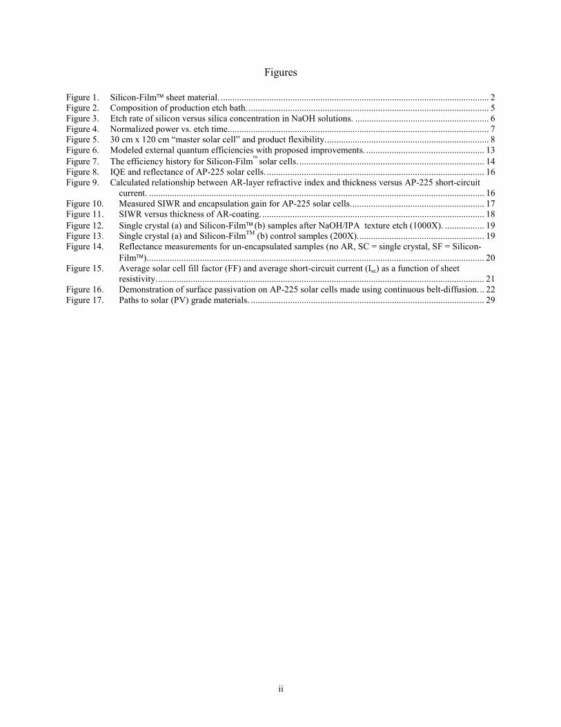
Figure 1. Silicon-Film sheet material.
The Silicon-Film process is presently in production at a new 9 MW nameplate capacitymanufacturing facility which started production in 1998. The present process is based on a 240cm2 solar cell (AP-225). Efficiencies exceeding 12% have been measured for the AP-225.Small, laboratory-scale devices have demonstrated efficiencies as high as 16.6%.
The approach and accomplishments in this report focus on the concept of “flexible” solarcell manufacturing. This involves continuation of engineering efforts to generate large areas ofhigh-quality Silicon-Film sheet material at high speeds and to implement new cassette-less,in-line processing equipment for solar cell manufacture.
The areal dimensions of Silicon-Film wafers and solar cells increased from 10 x 10 cm2
to 15 x 15 cm2 during the AstroPower PVMaT-4 program. Solar cell fabrication processes arenow being designed and developed within the AstroPower PVMaT-5 program to process large-area (30 x 120 cm2) Silicon-Film planks into solar cells.
During Phase I of this PVMaT program, significant progress has been made indeveloping large-area, in-line process machines for AR coating, belt gettering, belt diffusion, hotcaustic surface etching, and diffusion oxide etching. A large area, high-speed solar cell test/sortmachine was designed, fabricated and commissioned for the new manufacturing facility. Large-area semi-automatic screen printers and collocators were commissioned along with 36”-widecontact firing furnaces. Further metallization improvements are expected during the next twophases of the AstroPower PVMaT effort, and a new Silicon-Film sheet generation machinewith twice the throughput of the present machine will be constructed during Phase II based ondesigns established during the Phase I effort.
3
Approach
There are three basic development areas that are involved in transferring Silicon-Filmtechnology from the laboratory to the factory:
• Optimization of the sheet generation process -- high-speed, high quality, and largeareas are desired.
• Optimization of the solar cell fabrication sequence to achieve high efficiency withlarge areas. These processes must be compatible with manufacturing and shouldbe in-line and continuous rather than batch-mode.
• Integration of these developments in an industrial setting by the generation andsale of significant quantities of solar cells.
To achieve these broad objectives, AstroPower directed 1998 PVMaT developmentefforts into the following distinct tasks:
Task 1. In-Line Wet Processing.Task 2. Continuous Metallization.Task 3. New High-Throughput Sheet Machine.Task 4. Solar Cell Efficiency and Module Cost-Reduction Improvement.Task 4A. Increased Efficiency of Production Solar Cells.Task 4B. Metallurgical-Grade Silicon for Solar Application.Task 4C. Reduced Silicon Consumption through Recycling.
Results
In-Line Wet Processing
The goal of this task is to develop a set of production tools capable of processing largesheets of Silicon-Film material using a cassette-less in-line approach. In Phase I, we achievedthe following results.
• Purchased and installed an in-line Rinser-Dryer system in the new production facility. Useof this apparatus has resulted in a significant increase in throughput and quality compared tocassette-based spin-dry systems.
• Fabricated and evaluated a first-generation prototype hot caustic etching system. The resultsof this effort have formed the basis for a rigorous understanding of the chemistry of theNaOH-Si-H2O-SixOy system and the suitability of various wetted materials and componentsexposed to hot, concentrated caustic solutions. In 1999, a second-generation prototype willbe designed and assembled to further develop this process.
• Evaluated a number of potential in-line dilute HF “deglazing” systems for removal ofdiffusion oxides. We are currently in the final selection and specification process and expectto install and evaluate this system in 1999. After the evaluation process, it is expected thatthis machine will be directly transferred to production.
4
Continuous In-line Wafer Rinse-Dry System
To investigate the in-line wafer handling approach, a continuous wafer rinser-drier wasspecified and procured. This equipment is based on standard modular units consisting of load,rinse, dry, and unload sections. Each module is able to stand alone, but is bolted together to forma system. The results achieved with this continuous, in-line rinser-dryer system have beenimpressive. Wafers travel through the system at a speed of about 50 inches per minute. At thisspeed with maximum loading, the throughput of this system is over 2500 AP-225 wafers perhour. For comparison, a spin drier would take more than ten minutes to dry four cassettes (or100 wafers).
Based on the performance and reliability of this initial rinser-dryer system withproduction quantities of AP-225 Silicon-Film wafers, we have concluded that this type of in-line wet process equipment is the correct path for further wet process development. Large-areawafers or even full-width planks can also be processed with this type of equipment.
Continuous In-Line Pre-Getter Surface Preparation
Several cassette-based chemical process steps, including surface preparation prior to thegettering process and oxide strip following junction diffusion, exist in the current solar cellproduction line. These labor intensive chemical processes require the wafers to be loaded intocassettes, moved between chemical tanks by hand, dried in cassettes, and then unloaded. Themaximum wafer size is limited by the cassette size, and the total throughput is limited by thetank size. Also batch processes such as this are difficult to control, and the use of cassettes inprocessing reduces the liquid flow to the wafers and at times results in uneven etching andcleaning at the edges.
The implementation of an in-line wet chemical processing system would eliminate manyof the limitations discussed above. Such a system would be capable of handling wafers ofvarious sizes, even uncut Silicon-FilmTM planks. Operator exposure to chemicals would beminimized by a completely enclosed system where dry wafers are loaded for processing andcompletely rinsed and dried before being unloaded from the system. The composition of theprocess solutions would be maintained within operating limits by in-line monitoring and control.Such control would reduce raw material use and waste stream volume. Throughput of the in-linesystem would no longer be limited by tank size and the time consuming cassette loading andunloading operations. Total processing time would be further reduced by the more efficientcassette-less rinsing and drying steps.
Experimental Determination of Sodium Hydroxide and Silica Concentration
Determination of both NaOH and SiO2 concentrations in etch solution is a critical firststep to etch bath characterization, which is necessary for process automation, therefore severalanalytical techniques have been investigated. Gravimetric, titration and colorimetric methodshave been considered for silica concentration determination. The gravimetric method was foundto be unreliable because silicates can precipitate out as silica, silicate polymers (gels), or in manyother forms of hydrated silica. The titration method, if performed carefully, is extremely
5
accurate. Both sodium hydroxide and silica concentration of a standard solution weredetermined within 0.5wt. %. A drawback to this procedure is the time required for titration (oneor more hours if done by hand). Two colorimetric methods for determining silica concentrationwere evaluated. Both methods involve the conversion of silica to a colored complex andmeasurement of the intensity of light of a specific wavelength transmitted through the sample.The intensity of the analyzed sample is related to the total silica concentration. The colorimetricmethod is less accurate, but significantly faster, than the titration method.
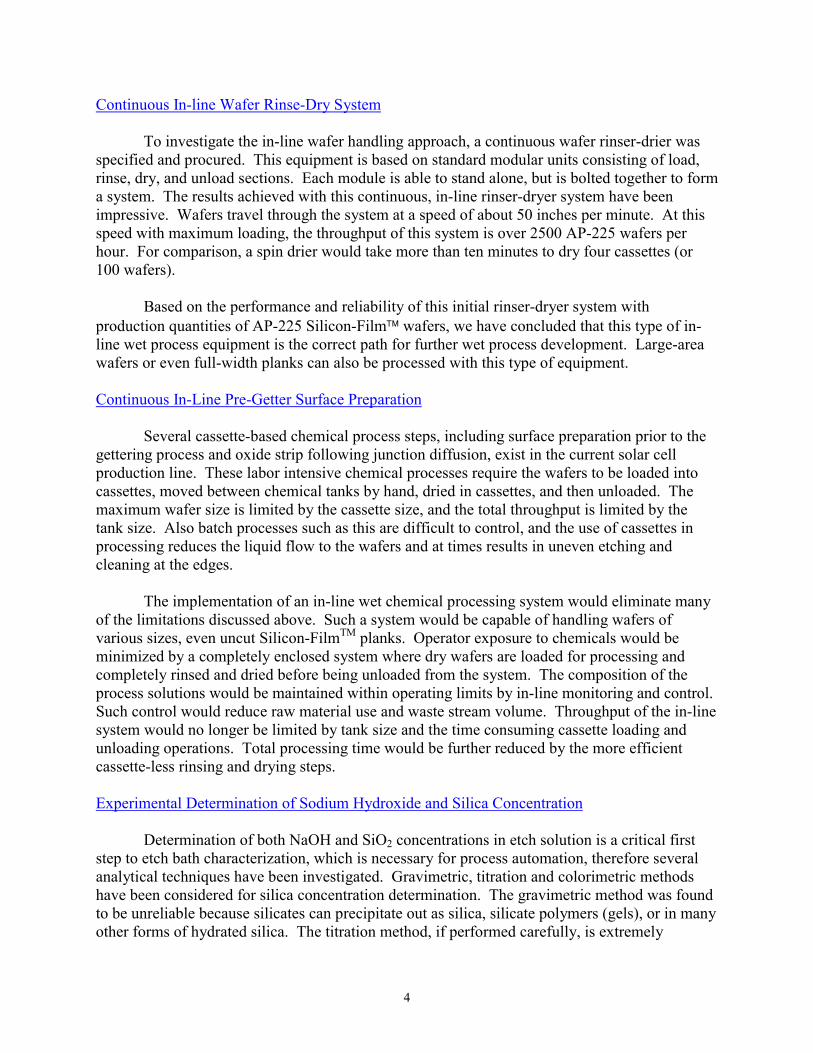
The analytical techniques developed for SiO2 and NaOH determination were applied toetch tanks for monitoring purposes. The concentration of NaOH and SiO2 both increased withthe number of wafers etched (Figure 2). The increase in silica concentration was expected andcorresponded to theoretical values. The increase in sodium hydroxide concentration was notexpected. Further experiments were conducted, from which it was determined that NaOHrefresh, periodic addition of sodium hydroxide to the etch tank to maintain constant NaOHconcentration during etching, exceeded NaOH consumption. As a result of this work sodiumhydroxide usage was cut in half with further reductions expected.
0
10
20
30
40
50
60
0 500 1000 1500 2000 2500 3000
WAFERS ETCHED
NaO
H, S
iOx
CO
NC
EN
TR
AT
ION
(%
)
0
10
20
30
40
50
60
Maximum Desired Silica Concentration to Inhibit "Staining"
Maximum Desired NaOH Concentration
NaOH
SiO2
NaOH Process Window(15 - 40 wt. %)
Figure 2. Composition of production etch bath.
Etch Rate Determination
The etch rate of Silicon-FilmTM wafers in sodium hydroxide was investigated in order todesign a production-scale in-line etch machine. Such information is crucial in determining etchtime and machine length. Laboratory-scale experiments were conducted to determine the factorsaffecting etch rate.
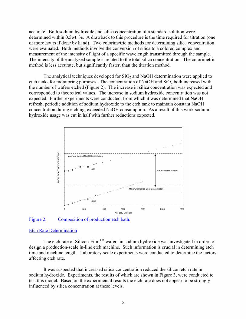
It was suspected that increased silica concentration reduced the silicon etch rate insodium hydroxide. Experiments, the results of which are shown in Figure 3, were conducted totest this model. Based on the experimental results the etch rate does not appear to be stronglyinfluenced by silica concentration at these levels.
6
0.0E+00
1.0E-04
2.0E-04
3.0E-04
4.0E-04
5.0E-04
6.0E-04
7.0E-04
8.0E-04
9.0E-04
1.0E-03
0 2 4 6 8 10 12 14
SiO2 CONCENTRATION (wt %)
ET
CH
RA
TE
(cm
/min
)
Single CrystalSilicon FilmSingle CrystalSilicon Film
Figure 3. Etch rate of silicon versus silica concentration in NaOH solutions.
Since silica concentration was found not to have a significant influence on etch rate, therelationship between etch rate and NaOH concentration was investigated. Another small-scaleetch rate experiment was performed. Results similar to the KOH/Si etch system were expected.The KOH/Si system was presented by Seidel, et al. [1] where, for a constant temperature of72°C, the etch rate of silicon in KOH:H2O solutions dropped off significantly for KOHconcentrations greater than 30 wt%. However, in the same reference, Seidel demonstrated thatthe etch rate dependence on temperature is stronger than its dependence on hydroxideconcentration. For this reason, the expected drop off in etch rate at high NaOH concentrationswas not observed due to temperature fluctuations in the reaction vessel. Therefore, in order tocontrol etch rate in production tanks, the temperature needs to be strictly controlled while thesodium hydroxide concentration can be allowed to fluctuate in a specified range.
In-line Pre-getter Etch
We constructed and evaluated the first prototype of the in-line etch system. Thisexperimental model has the capacity to hold one AP-225 wafer during the caustic etch step of thesurface preparation process. Rinsing and neutralization steps are performed manually.
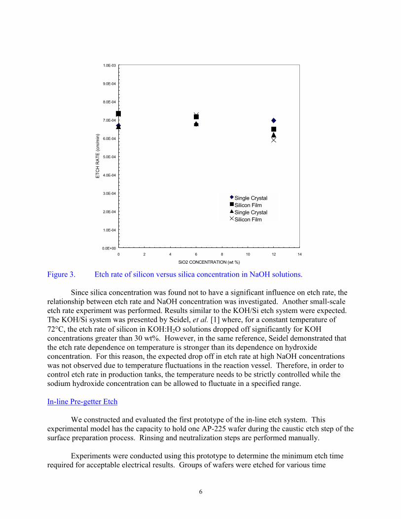
Experiments were conducted using this prototype to determine the minimum etch timerequired for acceptable electrical results. Groups of wafers were etched for various time
7
intervals at constant etch temperature. These samples were then processed into solar cells usingstandard manufacturing processes. Figure 4 shows a sample of the test results where power hasbeen normalized against the average power of standard solar cells, and the etch interval wasnormalized with respect to standard production etch time. These data show a significant increasein solar cell electrical performance as the etch time increases. However, for etch times more thantwice the standard production time, performance begins to level off.
0.700
0.750
0.800
0.850
0.900
0.950
1.000
1.050
1.100
1.150
1.200
0.5 1 1.5 2 2.5 3
Etch Time Normalized to Standard Production Time
No
rmal
ized
Pm
ax
Float Etch
STD Etch
Poly. (Float Etch)
STD Temp
STD Temp - 10 Deg. C
Figure 4. Normalized power vs. etch time.
We have begun the design of the next prototype etching system, which will be used todevelop the wafer transport system. It will be a single-track system (one wafer wide) andconsists of two sections: etch and rinse. All of the sumps, pumps and filters will be self-contained. Two additional process steps consisting of a spray rinse and dry can be added. Thesemodules are the same as those which were successfully demonstrated by the previouslymentioned rinser-dryer system.
In-Line Diffusion Oxide Deglaze System
During the diffusion process a thin layer of phosphorus-doped silicon dioxide grows atthe surfaces of the wafers. This oxide must be removed prior to the contact metallization steps;usually this is accomplished by briefly etching the wafers in a dilute hydrofluoric (HF) acidsolution. At present, the etching process is cassette based and performed in wet process tanks ina chemical fume hood. Once the diffusion oxide is etched, the wafers are unloaded from thecassettes so that they can proceed to the next process step.
8
Changing from a batch to in-line diffusion oxide strip is expected to significantlyimprove the process and reduce both material use and the waste stream volume. Such in-linesystems also minimize operator exposure to process chemistries due to the fact that mostmodules are self-contained. Because of the modular design approach, this type of equipment isadaptable for silicon plank as well as solar cell processing. A diffusion oxide etching system forSilicon-Film wafers might consist of an HF-etch process module, a rinse module, and a drymodule, along with any required loader and unloader sections. Since the in-line chemical etchsystem is cassette-less, we expect labor cost to be reduced and throughput to be increased. In thefollowing year AstroPower will purchase such a unit and begin experiments with Silicon-Filmwafers.
Continuous Metallization
The goal of this task is to assess technologies that are suitable for applying front and backcontact metallization to Silicon-Film with the intent of handling larger solar cells and planks.Cutting the plank to final solar cell size will be moved to a much later step in the processsequence. Much of the work carried out in Phase I focused on equipment and inks for screenprinting. Progress also occurred with the development/deployment of new contact firingfurnaces, belt-loading collocators, ink formulations, screen printing screens, and with varioussolar cell sizes.
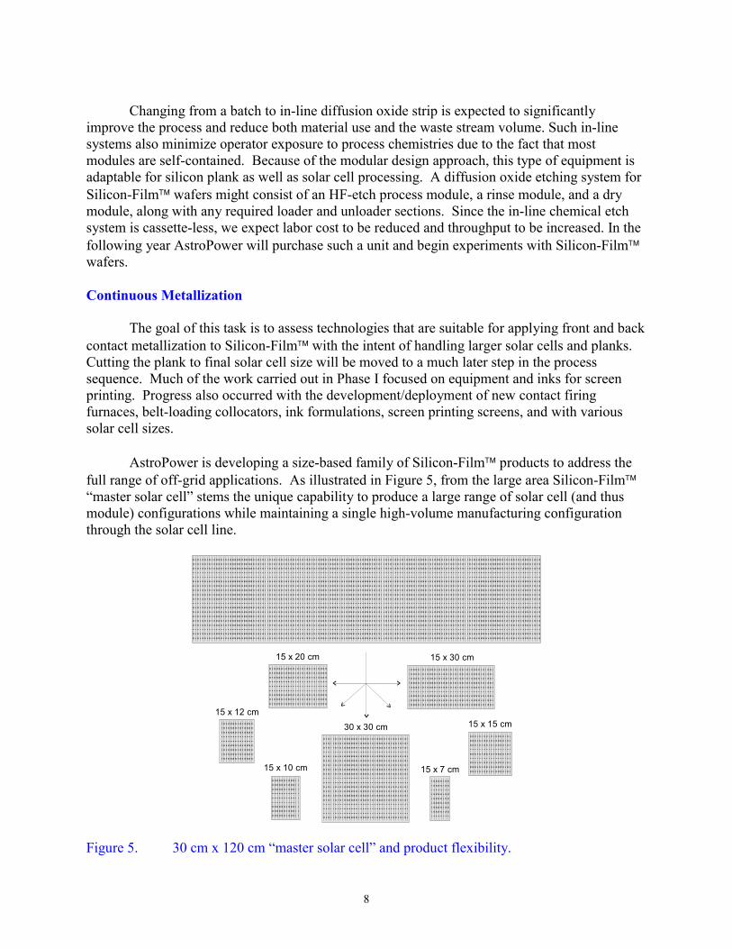
AstroPower is developing a size-based family of Silicon-Film products to address thefull range of off-grid applications. As illustrated in Figure 5, from the large area Silicon-Film“master solar cell” stems the unique capability to produce a large range of solar cell (and thusmodule) configurations while maintaining a single high-volume manufacturing configurationthrough the solar cell line.
30 x 30 cm
15 x 30 cm
15 x 15 cm
15 x 10 cm
15 x 20 cm
15 x 12 cm
15 x 7 cm
Figure 5. 30 cm x 120 cm “master solar cell” and product flexibility.
9
During Phase I, we achieved the following results in Task 2.
• Screen printed a 30 x 30 cm2 AP-900 prototype solar cell using a deHaart screenprinter. This demonstrates the compatibility of large-area Silicon-Film materialwith standard screen printing equipment.
• Installed and commissioned 36-inch wide belt furnaces in both productionfacilities for high-temperature cell processing. These furnaces are used for belt-gettering, belt-diffusion, and front and back metallization process steps. Thesesignificantly wider belt furnaces have greatly increased throughput in all theseprocesses.
• Installed and commissioned semi-automatic screen printers with furnace-belt-loadcollocators that are matched to the 36-inch wide belt furnaces.
• Investigated new contact metallization ink formulations.• Investigated new types of screens for printing fine lines.• Designed metallization patterns for the “family” of proposed Silicon-Film-based
products.• Evaluated and assessed other potential metallization technologies.
Large-area belt furnaces
Prior to this contract, the widest infrared belt furnace available for solar cell processingwas 24 inches wide and the fastest screen printers were supplied with collocators (belt loaders)matched to this 24 inch width. Our analysis has shown that, for an in-line process such as plankproduction or metallization firing, increasing the width of the system yields a significantimprovement in process costs.
Discussions with a furnace manufacturer resulted in the conclusion that it was feasible toproduce a 36-inch wide furnace and that the capital cost of a wider furnace is not significantlyhigher than a 24 inch system. During Phase I, we developed a specification for a 36-inch widemetallization firing furnace. Four furnaces have been purchased and installed in AstroPowerfacilities.
Screen printers are supplied with collocators which are matched to the width of theprocess furnace. The widest collocator available before Phase I was 24 inches. Two screenprinter manufacturers were asked to provide screen printers with new, wider collocators to matchthe 36 inch furnaces. One manufacturer agreed to re-design an existing collocator system andintegrate it with a standard screen printer. Two of these wide-collocator screen printers werepurchased and commissioned in the Pencader facility.
Low contact resistance ink
We have begun to work with an ink manufacturer on new front contact inks that wouldresult in lower contact resistance. Our initial meeting took place at the end of Phase I, and awork plan was developed. The manufacturer has agreed to provide experimental silver frontcontact inks (200 gm samples) to AstroPower. In return, AstroPower will test the inks by
10
fabricating solar cells with different time-temperature sintering schedules and will provide IVdata, particularly series resistance information.
High resolution screen printing
Shadowing by the grid metallization is a significant loss mechanism for screen printedsolar cells. Shadowing is a function of the wafer surface characteristics, the metal inkformulation, the screen printer settings, the screen pattern, and the screen itself. During Phase Iwe investigated the effect of calendered, elliptical rather than round wire, screens on gridlinewidth and shadowing. Calendered screens offer the possibility of printing taller and finer lineson the front surface of solar cells, reducing both shading and Rs losses.
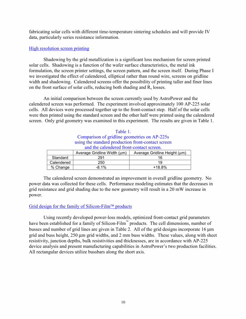
An initial comparison between the screen currently used by AstroPower and thecalendered screen was performed. The experiment involved approximately 100 AP-225 solarcells. All devices were processed together up to the front-contact step. Half of the solar cellswere then printed using the standard screen and the other half were printed using the calenderedscreen. Only grid geometry was examined in this experiment. The results are given in Table 1.
Table 1.Comparison of gridline geometries on AP-225s
using the standard production front-contact screenand the calendered front-contact screen.
Average Gridline Width (µm) Average Gridline Height (µm)Standard 291 16
Calendered 250 19% Change -8.1% +18.8%
The calendered screen demonstrated an improvement in overall gridline geometry. Nopower data was collected for these cells. Performance modeling estimates that the decreases ingrid resistance and grid shading due to the new geometry will result in a 20 mW increase inpower.
Grid design for the family of Silicon-Film products
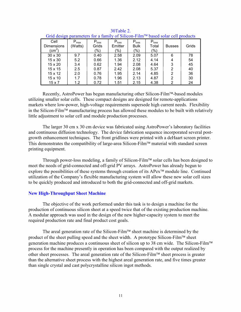
Using recently developed power-loss models, optimized front-contact grid parametershave been established for a family of Silicon-Film products. The cell dimensions, number ofbusses and number of grid lines are given in Table 2. All of the grid designs incorporate 16 µmgrid and buss height, 250 µm grid widths, and 2 mm buss widths. These values, along with sheetresistivity, junction depths, bulk resistivities and thicknesses, are in accordance with AP-225device analysis and present manufacturing capabilities in AstroPower’s two production facilities.All rectangular devices utilize bussbars along the short axis.
11
30Table 2.Grid design parameters for a family of Silicon-Film based solar cell products
CellDimensions
(cm2)
Pmax
(Watts)Ploss
Grids(%)
Ploss
Emitter(%)
Ploss
Bulk(%)
Ploss
Total(%)
Busses Grids
30 x 30 9.7 0.40 2.58 2.09 5.07 6 7815 x 30 5.2 0.66 1.36 2.12 4.14 4 5415 x 20 3.4 0.62 1.94 2.08 4.64 3 4515 x 15 2.5 0.87 2.42 2.08 5.37 2 4015 x 12 2.0 0.76 1.95 2.14 4.85 2 3615 x 10 1.7 0.78 1.96 2.13 4.87 2 3015 x 7 1.2 0.72 1.51 2.15 4.38 2 24
Recently, AstroPower has begun manufacturing other Silicon-Film-based modulesutilizing smaller solar cells. These compact designs are designed for remote-applicationsmarkets where low-power, high-voltage requirements supersede high current needs. Flexibilityin the Silicon-Film manufacturing process has allowed these modules to be built with relativelylittle adjustment to solar cell and module production processes.
The larger 30 cm x 30 cm device was fabricated using AstroPower’s laboratory facilitiesand continuous diffusion technology. The device fabrication sequence incorporated several post-growth enhancement techniques. The front gridlines were printed with a deHaart screen printer.This demonstrates the compatibility of large-area Silicon-Film material with standard screenprinting equipment.
Through power-loss modeling, a family of Silicon-Film solar cells has been designed tomeet the needs of grid-connected and off-grid PV arrays. AstroPower has already begun toexplore the possibilities of these systems through creation of its APex module line. Continuedutilization of the Company’s flexible manufacturing system will allow these new solar cell sizesto be quickly produced and introduced to both the grid-connected and off-grid markets.
New High-Throughput Sheet Machine
The objective of the work performed under this task is to design a machine for theproduction of continuous silicon sheet at a speed twice that of the existing production machine.A modular approach was used in the design of the new higher-capacity system to meet therequired production rate and final product cost goals.
The areal generation rate of the Silicon-Film sheet machine is determined by theproduct of the sheet pulling speed and the sheet width. A prototype Silicon-Film sheetgeneration machine produces a continuous sheet of silicon up to 38 cm wide. The Silicon-Filmprocess for the machine presently in operation has been compared with the output realized byother sheet processes. The areal generation rate of the Silicon-Film sheet process is greaterthan the alternative sheet process with the highest areal generation rate, and five times greaterthan single crystal and cast polycrystalline silicon ingot methods.
12
The high areal generation rate of Silicon-Film sheet demonstrates the production rateadvantage of the AstroPower process for producing large areas of crystalline silicon forprocessing into solar cells. There are other advantages as well. The thermal profiles employedin Silicon-Film growth lead to a reduction in thermal stress-induced material defects. Incontrast, the large temperature gradients employed by other sheet generation techniques make itdifficult to fabricate wide sheets (>10 cm). It is also well known that reducing thermally-inducedstress in the material reduces breakage during solar-cell processing.
During Phase I, AstroPower completed the design of a Silicon-Film sheet machine. Aseries of tests were conducted on the present production machine that enabled the generation ofdata to drive the model for the high-throughput machine. A modular approach was employed toset the design for the three major process zones taking into account the specific thermal,chemical, electrical and mechanical attributes required to effect the process in each zone. Long-lead-time items have been identified and those parts have been ordered. The construction of thenew machine will begin during Phase II.
Solar Cell Efficiency and Module Cost-Reduction Improvement
The goal of this task is to investigate process and characterization techniques to increasesolar cell efficiency and lower module costs. In 1998, we achieved the following results.
• Developed an in-line AR coating system capable of coating large-area Silicon-Film solar cells.
• Evaluated the RF-PCD technique as a contactless material quality assessmenttool. These results indicate that the RF-PCD technique is predictive of short-circuit current for devices with junctions. In 1999, we will continue to investigatethe RF-PCD and other potential techniques with the goal of predicting theperformance of as-grown Silicon-Film sheet material.
• Developed and improved continuous in-line gettering and diffusion processes toimprove the diffusion length, current generation, fill factor, and efficiency ofSilicon-Film AP-225 solar cells.
• Designed a new junction box for all AstroPower module products. This junctionbox is in the process of being UL approved. Higher current (over 10 A) bypassdiodes for large-area solar cells and modules were identified. These diodes are inthe process of being qualified.
• Installed and commissioned a Spire stringer-tabber system to further mechanizemodule assembly. This system was specified for application to AP-225 solar cellmodule production. Two large-area laminators were installed and commissioned.One manufactured by Spire and one by NPC.
• Designed, constructed, and commissioned a new automatic solar cell tester-sortersystem for AP-225 solar cells. This flexible system is capable of handling andtesting large-area cells up to 8” (AP-400).
The objective of the work performed under this Task is to develop advanced processingtechniques that increase the efficiency of production Silicon-Film solar cells. This reportsummarizes work performed to enhance solar cell performance by optimizing production
13
processes related to module and device optics, the emitter or “blue response” of AP-225 solarcells and the bulk or “red response” of Silicon-Film material.
A detailed characterization of a typical AP-225 solar cell reveals that the short-circuitcurrent is limited by losses in blue response, red response, and optical transmission. These lossmechanisms and associated issues can be further detailed as:
• Device optics: grid shading, AR coating, and surface morphology• Blue response: junction formation, surface passivation, and metallization• Red response: growth and post-growth improvement, characterization
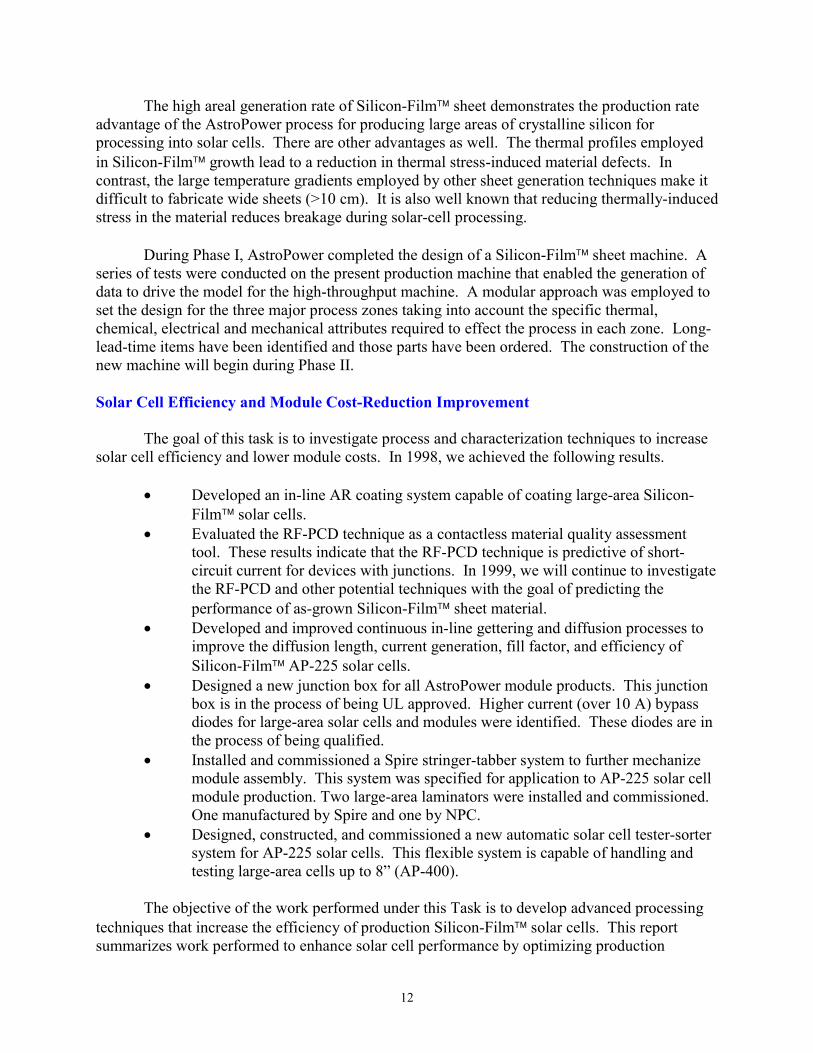
To understand the potential improvements in short-circuit current, solar cell models havebeen developed to predict increases in current as improvements in each of the three areas areachieved. The calculated external quantum efficiencies for the production AP-225 solar cell areillustrated in Figure 6. This analysis shows that there is potentially a 1.4 A (26%) increase in theshort-circuit current of an AP-225 solar cell as the fabrication process is improved.
0
10
20
30
40
50
60
70
80
90
100
350 450 550 650 750 850 950 1050 1150
Wavelength, nm
Ext
ern
al Q
E, %
Improve Red, Isc=6.73A
Improve blue, Isc=6.38A
Improve Optics, Isc=5.88A
Baseline, Isc=5.32A
Figure 6. Modeled external quantum efficiencies with proposed improvements.
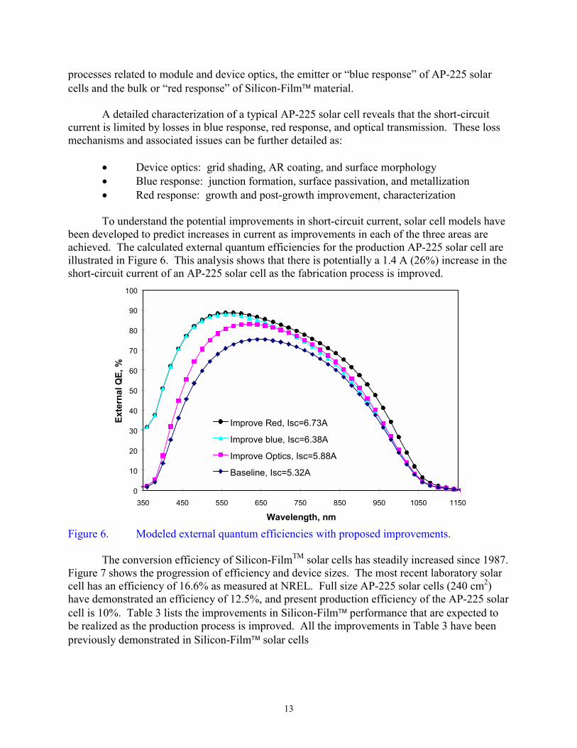
The conversion efficiency of Silicon-FilmTM solar cells has steadily increased since 1987.Figure 7 shows the progression of efficiency and device sizes. The most recent laboratory solarcell has an efficiency of 16.6% as measured at NREL. Full size AP-225 solar cells (240 cm2)have demonstrated an efficiency of 12.5%, and present production efficiency of the AP-225 solarcell is 10%. Table 3 lists the improvements in Silicon-Film performance that are expected tobe realized as the production process is improved. All the improvements in Table 3 have beenpreviously demonstrated in Silicon-Film solar cells
14
Figure 7. The efficiency history for Silicon-Film solar cells.
Table 3.Proposed improvements in Silicon-FilmTM solar cells
Area forImprovement
Isc
(A)Jsc
(mA/cm2)Voc
(V)FF(%)
Power(W)
η(%)
Present case(improved optics)
6.31 26.3 0.539 71.8 2.44 10.14
Improved Blueresponse
6.98 29.1 0.542 72.3 2.74 11.36
Improved FF 6.99 29.1 0.547 75.3 2.88 11.97
The blue response of a typical Silicon-Film solar cell is lower than the present industrystandard. Blue response, the ability to convert photons at the high energy end of the solarspectrum to usable charge carriers, is sensitive to the specifics of the junction and to passivationof the silicon surface. The electrical resistance of the metal contacts to the diffused layer is alsosensitive to the specifics of the junction diffusion. The speed with which the AP-225 was takento production required the use of a simple junction design and diffusion process to enhancecontact conductivity. The path to improved response is extensively detailed in the literature.Improved blue response requires optimization of the diffusion design to minimize contactresistance, and incorporation of surface passivation. The latter can be done as part of theantireflection coating.
Diffusion length represents the single largest area for improvement for Silicon-Filmmaterial. Several efforts have been undertaken to explain the presence of long diffusion lengthsthat occur sporadically in Silicon-Film as-grown material. Diffusion lengths as high as 200 µmin as-grown material have been measured, with many readings in the 100 to 200 µm range.Achieving 200 µm diffusion lengths will result in production efficiencies of 16.3%.
The fill factor improvements shown in Table 3 highlight several device issues such ascontact resistance and imperfect isolation. The leakage current (J02) is associated with defects inthe space charge region of the diode. All of the characteristics spelled out in Table 3 have beendemonstrated at their target values in full size production solar cells that have been fabricated
15
with advanced processing. For example, the leakage current (J02) has been reduced to the targetlevel by reducing the surface texture and modifying the junction diffusion.
Advanced Processing Work and Results
Optimization of Solar Cell Optics
The objective of the work performed under this Task is to develop advanced processingtechniques that increase the efficiency of production Silicon-Film solar cells. This reportsummarizes the work performed during Phase I to enhance solar cell performance by optimizingproduction processes related to module and device optics. Work in this area is currently focusingon:
• Reduction of gridline width• Optimization of AR-coating thickness and index of refraction• Texturing of the wafer surface for improved light-trapping
Reduced Gridline Width
A video monitoring system has recently been installed in the Silicon-Film productionfacility. This system has been designed to assist the front contact metallization operators inroutine monitoring of AP-225 gridline height and width. Previously, this critical step wasperformed with a simple optical microscope. This new system effectively decreases the timerequired for gridline inspection by a factor of two. Also, the video system allows operatorssupervisors, and engineers to view potential defects simultaneously. This new system hasimproved communication between technical and operating personnel resulting in greaterthroughput, less downtime, and greater precision and control in Silicon-Film research deviceprocessing.
Optimized AR-coating Thickness and Index of Refraction
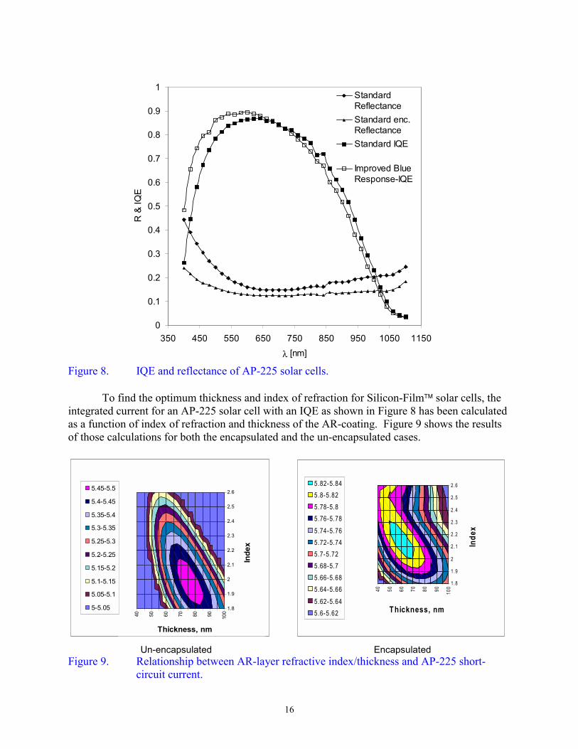
Optimal AR-coating layer parameters (thickness and index of refraction) have beenpredicted for both encapsulated and un-encapsulated cases. Reflection properties of TiO2-coatedSilicon-Film surfaces are being evaluated and the deposition conditions are being tuned totarget the optimal thickness and index to achieve minimal reflection losses.
Figure 8 shows reflectance and IQE data for a typical AP-225 solar cell as well as IQE ofan AP-225 solar cell with improved blue response. Due to the short diffusion length of AP-225solar cells it is important that the reflectance minimum of the AR-coating is matched to the peakof the IQE. From Figure 8 it is clear that the solar cell with improved blue response needs athinner AR-coating than the standard AP-225 solar cell. A thinner AR-coating will shift theminimum of the reflection curve to lower wavelengths, agreeing better with the maximum of theIQE curves.
16
0
0.1
0.2
0.3
0.4
0.5
0.6
0.7
0.8
0.9
1
350 450 550 650 750 850 950 1050 1150
λ [nm]
R &
IQE
StandardReflectance
Standard enc.Reflectance
Standard IQE
Improved BlueResponse-IQE
Figure 8. IQE and reflectance of AP-225 solar cells.
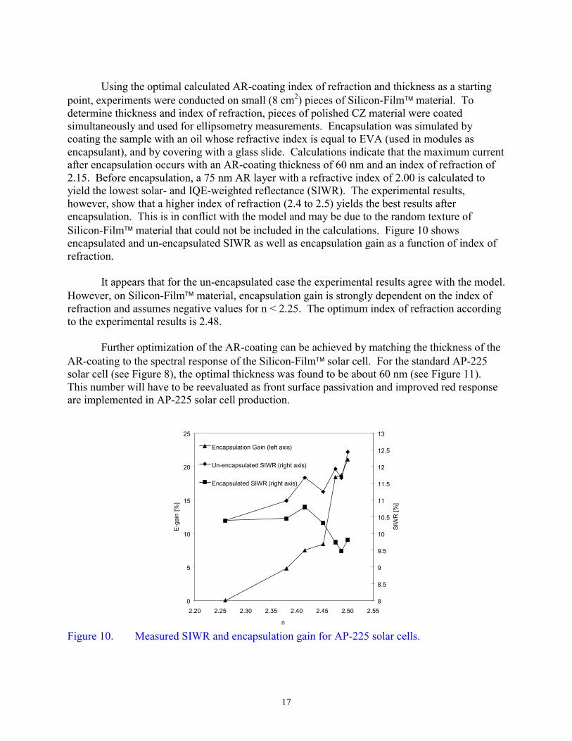
To find the optimum thickness and index of refraction for Silicon-Film solar cells, theintegrated current for an AP-225 solar cell with an IQE as shown in Figure 8 has been calculatedas a function of index of refraction and thickness of the AR-coating. Figure 9 shows the resultsof those calculations for both the encapsulated and the un-encapsulated cases.
40 50 60 70 80 90 100
1.8
1.9
2
2.1
2.2
2.3
2.4
2.5
2.6
Thickness, nm
Ind
ex
5.45-5.5
5.4-5.45
5.35-5.4
5.3-5.35
5.25-5.3
5.2-5.25
5.15-5.2
5.1-5.15
5.05-5.1
5-5.05
40 50 60 70 80 90 100
1 .8
1 .9
2
2.1
2 .2
2 .3
2 .4
2 .5
2 .6
T hickness, nm
Inde
x5.82-5.845.8-5.825.78-5.85.76-5.78
5.74-5.765.72-5.745.7-5.725.68-5.75.66-5.685.64-5.66
5.62-5.645.6-5.62
Un-encapsulated EncapsulatedFigure 9. Relationship between AR-layer refractive index/thickness and AP-225 short-
circuit current.
17
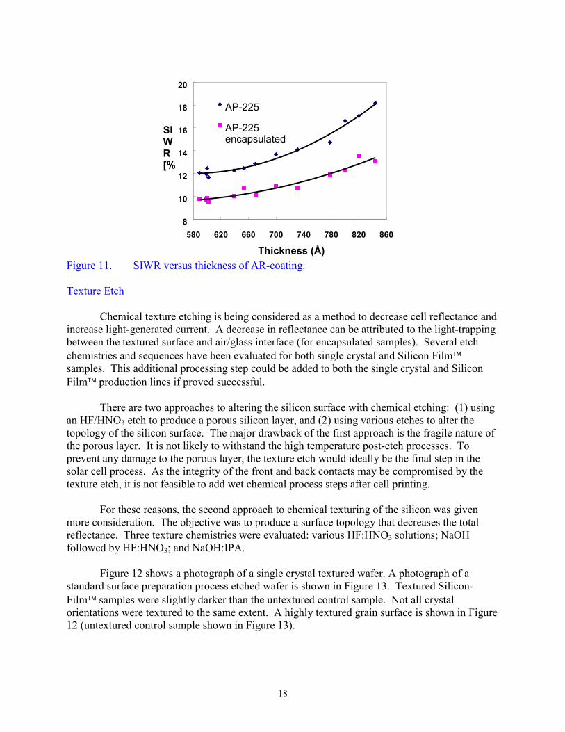
Using the optimal calculated AR-coating index of refraction and thickness as a startingpoint, experiments were conducted on small (8 cm2) pieces of Silicon-Film material. Todetermine thickness and index of refraction, pieces of polished CZ material were coatedsimultaneously and used for ellipsometry measurements. Encapsulation was simulated bycoating the sample with an oil whose refractive index is equal to EVA (used in modules asencapsulant), and by covering with a glass slide. Calculations indicate that the maximum currentafter encapsulation occurs with an AR-coating thickness of 60 nm and an index of refraction of2.15. Before encapsulation, a 75 nm AR layer with a refractive index of 2.00 is calculated toyield the lowest solar- and IQE-weighted reflectance (SIWR). The experimental results,however, show that a higher index of refraction (2.4 to 2.5) yields the best results afterencapsulation. This is in conflict with the model and may be due to the random texture ofSilicon-Film material that could not be included in the calculations. Figure 10 showsencapsulated and un-encapsulated SIWR as well as encapsulation gain as a function of index ofrefraction.
It appears that for the un-encapsulated case the experimental results agree with the model.However, on Silicon-Film material, encapsulation gain is strongly dependent on the index ofrefraction and assumes negative values for n < 2.25. The optimum index of refraction accordingto the experimental results is 2.48.
Further optimization of the AR-coating can be achieved by matching the thickness of theAR-coating to the spectral response of the Silicon-Film solar cell. For the standard AP-225solar cell (see Figure 8), the optimal thickness was found to be about 60 nm (see Figure 11).This number will have to be reevaluated as front surface passivation and improved red responseare implemented in AP-225 solar cell production.
0
5
10
15
20
25
2.20 2.25 2.30 2.35 2.40 2.45 2.50 2.55
n
E-g
ain
[%
]
8
8.5
9
9.5
10
10.5
11
11.5
12
12.5
13
SIW
R [
%]
Encapsulation Gain (left axis)
Un-encapsulated SIWR (right axis)
Encapsulated SIWR (right axis)
Figure 10. Measured SIWR and encapsulation gain for AP-225 solar cells.
18
8
10
12
14
16
18
20
580 620 660 700 740 780 820 860
Thickness (Å)
SIWR[%
AP-225
AP-225encapsulated
Figure 11. SIWR versus thickness of AR-coating.
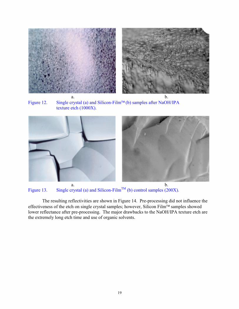
Texture Etch
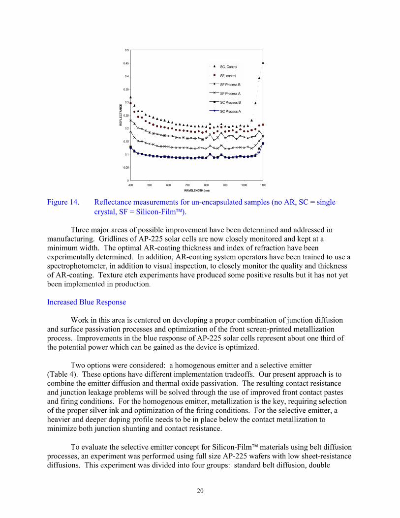
Chemical texture etching is being considered as a method to decrease cell reflectance andincrease light-generated current. A decrease in reflectance can be attributed to the light-trappingbetween the textured surface and air/glass interface (for encapsulated samples). Several etchchemistries and sequences have been evaluated for both single crystal and Silicon Filmsamples. This additional processing step could be added to both the single crystal and SiliconFilm production lines if proved successful.
There are two approaches to altering the silicon surface with chemical etching: (1) usingan HF/HNO3 etch to produce a porous silicon layer, and (2) using various etches to alter thetopology of the silicon surface. The major drawback of the first approach is the fragile nature ofthe porous layer. It is not likely to withstand the high temperature post-etch processes. Toprevent any damage to the porous layer, the texture etch would ideally be the final step in thesolar cell process. As the integrity of the front and back contacts may be compromised by thetexture etch, it is not feasible to add wet chemical process steps after cell printing.
For these reasons, the second approach to chemical texturing of the silicon was givenmore consideration. The objective was to produce a surface topology that decreases the totalreflectance. Three texture chemistries were evaluated: various HF:HNO3 solutions; NaOHfollowed by HF:HNO3; and NaOH:IPA.
Figure 12 shows a photograph of a single crystal textured wafer. A photograph of astandard surface preparation process etched wafer is shown in Figure 13. Textured Silicon-Film samples were slightly darker than the untextured control sample. Not all crystalorientations were textured to the same extent. A highly textured grain surface is shown in Figure12 (untextured control sample shown in Figure 13).
19
a. b.Figure 12. Single crystal (a) and Silicon-Film (b) samples after NaOH/IPA
texture etch (1000X).
a. b.Figure 13. Single crystal (a) and Silicon-FilmTM (b) control samples (200X).
The resulting reflectivities are shown in Figure 14. Pre-processing did not influence theeffectiveness of the etch on single crystal samples; however, Silicon Film samples showedlower reflectance after pre-processing. The major drawbacks to the NaOH/IPA texture etch arethe extremely long etch time and use of organic solvents.
20
0
0.05
0.1
0.15
0.2
0.25
0.3
0.35
0.4
0.45
0.5
400 500 600 700 800 900 1000 1100
WAVELENGTH (nm)
RE
FL
EC
TA
NC
E
SC, Control
SF, control
SF Process B
SF Process A
SC Process B
SC Process A
Figure 14. Reflectance measurements for un-encapsulated samples (no AR, SC = singlecrystal, SF = Silicon-Film).
Three major areas of possible improvement have been determined and addressed inmanufacturing. Gridlines of AP-225 solar cells are now closely monitored and kept at aminimum width. The optimal AR-coating thickness and index of refraction have beenexperimentally determined. In addition, AR-coating system operators have been trained to use aspectrophotometer, in addition to visual inspection, to closely monitor the quality and thicknessof AR-coating. Texture etch experiments have produced some positive results but it has not yetbeen implemented in production.
Increased Blue Response
Work in this area is centered on developing a proper combination of junction diffusionand surface passivation processes and optimization of the front screen-printed metallizationprocess. Improvements in the blue response of AP-225 solar cells represent about one third ofthe potential power which can be gained as the device is optimized.
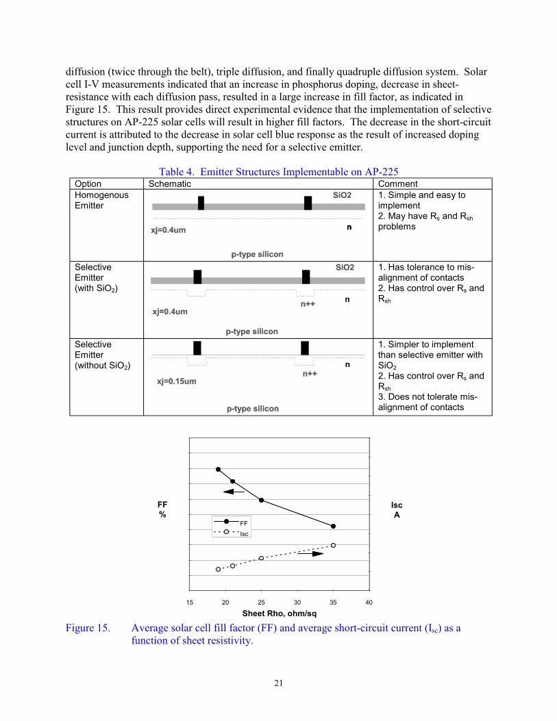
Two options were considered: a homogenous emitter and a selective emitter(Table 4). These options have different implementation tradeoffs. Our present approach is tocombine the emitter diffusion and thermal oxide passivation. The resulting contact resistanceand junction leakage problems will be solved through the use of improved front contact pastesand firing conditions. For the homogenous emitter, metallization is the key, requiring selectionof the proper silver ink and optimization of the firing conditions. For the selective emitter, aheavier and deeper doping profile needs to be in place below the contact metallization tominimize both junction shunting and contact resistance.
To evaluate the selective emitter concept for Silicon-Film materials using belt diffusionprocesses, an experiment was performed using full size AP-225 wafers with low sheet-resistancediffusions. This experiment was divided into four groups: standard belt diffusion, double
21
diffusion (twice through the belt), triple diffusion, and finally quadruple diffusion system. Solarcell I-V measurements indicated that an increase in phosphorus doping, decrease in sheet-resistance with each diffusion pass, resulted in a large increase in fill factor, as indicated inFigure 15. This result provides direct experimental evidence that the implementation of selectivestructures on AP-225 solar cells will result in higher fill factors. The decrease in the short-circuitcurrent is attributed to the decrease in solar cell blue response as the result of increased dopinglevel and junction depth, supporting the need for a selective emitter.
Table 4. Emitter Structures Implementable on AP-225Option Schematic CommentHomogenousEmitter
1. Simple and easy toimplement2. May have Rs and Rsh
problems
SelectiveEmitter(with SiO2)
1. Has tolerance to mis-alignment of contacts2. Has control over Rs andRsh
SelectiveEmitter(without SiO2)
1. Simpler to implementthan selective emitter withSiO2
2. Has control over Rs andRsh
3. Does not tolerate mis-alignment of contacts
65
66
67
68
69
70
71
72
73
74
75
15 20 25 30 35 40
Sheet Rho, ohm/sq
FF%
3.40
3.60
3.80
4.00
4.20
4.40
4.60
4.80
5.00
IscA
FF
Isc
Figure 15. Average solar cell fill factor (FF) and average short-circuit current (Isc) as afunction of sheet resistivity.
22
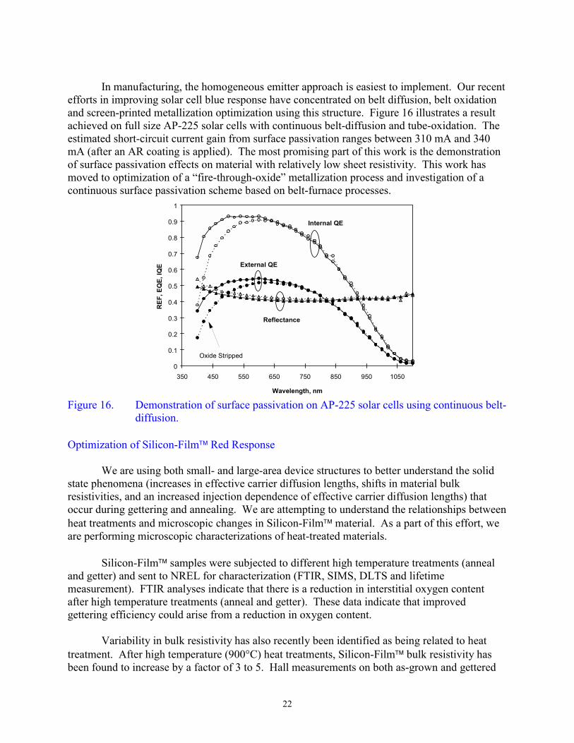
In manufacturing, the homogeneous emitter approach is easiest to implement. Our recentefforts in improving solar cell blue response have concentrated on belt diffusion, belt oxidationand screen-printed metallization optimization using this structure. Figure 16 illustrates a resultachieved on full size AP-225 solar cells with continuous belt-diffusion and tube-oxidation. Theestimated short-circuit current gain from surface passivation ranges between 310 mA and 340mA (after an AR coating is applied). The most promising part of this work is the demonstrationof surface passivation effects on material with relatively low sheet resistivity. This work hasmoved to optimization of a “fire-through-oxide” metallization process and investigation of acontinuous surface passivation scheme based on belt-furnace processes.
0
0.1
0.2
0.3
0.4
0.5
0.6
0.7
0.8
0.9
1
350 450 550 650 750 850 950 1050
Wavelength, nm
RE
F, E
QE
, IQ
E
Internal QE
External QE
Reflectance
Oxide Stripped
Figure 16. Demonstration of surface passivation on AP-225 solar cells using continuous belt-diffusion.
Optimization of Silicon-Film Red Response
We are using both small- and large-area device structures to better understand the solidstate phenomena (increases in effective carrier diffusion lengths, shifts in material bulkresistivities, and an increased injection dependence of effective carrier diffusion lengths) thatoccur during gettering and annealing. We are attempting to understand the relationships betweenheat treatments and microscopic changes in Silicon-Film material. As a part of this effort, weare performing microscopic characterizations of heat-treated materials.
Silicon-Film samples were subjected to different high temperature treatments (annealand getter) and sent to NREL for characterization (FTIR, SIMS, DLTS and lifetimemeasurement). FTIR analyses indicate that there is a reduction in interstitial oxygen contentafter high temperature treatments (anneal and getter). These data indicate that improvedgettering efficiency could arise from a reduction in oxygen content.
Variability in bulk resistivity has also recently been identified as being related to heattreatment. After high temperature (900°C) heat treatments, Silicon-Film bulk resistivity hasbeen found to increase by a factor of 3 to 5. Hall measurements on both as-grown and gettered
23
Silicon-Film material indicate that this resistivity increase is primarily due to a reduction incarrier mobility. The cause of this is not yet clear. More interestingly, as indicated by Dr.Richard Ahrenkiel at NREL, low temperature (~210°C) quench treatments also result in anincrease in bulk resistivity. Dr. Ahrenkiel has proposed that this behavior is related to thedissociation of Fe-B pairs in Silicon-Film material.
Module Cost Reductions
The objective of work performed under this Task is to reduce the cost of materials andprocesses associated with Silicon-Film module fabrication. Development efforts byAstroPower during Phase I of this contract were focussed primarily in three areas:
• Reduction of the cost of the junction box (J-box) assembly and the assemblytime;
• Reduction of the assembly time required to make the electrical connectionbetween the J-box and the laminate; and
• Reduction of the cost of the back sheet material.
AstroPower’s new Pencader facility (Newark, DE) for manufacturing solar cells and formodule assembly was dedicated in March 1998. A semi-automated tabber-stringer system waspurchased and commissioned for this facility, as was a large-area laminator. Additional ULapprovals for Silicon-Film module and panel products were obtained. Cooperative workbetween AstroPower and Evergreen Solar on module material cost reductions was postponeduntil a later date at their request.
The overall goal of the PVMaT-5A program at AstroPower is to engineer and developflexible manufacturing methods and equipment to process Silicon-Film solar cells andmodules. While primary emphasis has been placed on wafer and solar cell manufacturing areas,there are areas where incremental and significant improvements have been realized in Silicon-Film module design and manufacturing. Specifically, producing a frameless moduleeliminates the significant cost of the framing materials and the labor required to assemble it.Depending on the cost of the particular components used, the skill of the assembler, and the typeand quantity of fixtures and tools, this one change can impact the cost of high power modules by$0.25 per watt (the impact on lower power modules is even greater). Other significant costreductions have been realized by qualifying lower-cost commercially available bypass diodesthat replace custom-fabricated diodes. This has netted savings in the range of $12 to $14 permodule. The most time-consuming step in module assembly is the cell stringing operation.Although difficult to implement, automation of this operation will yield significant savings.Other improvements have been realized by purchasing or developing special tools and fixtures.For example, the RTV adhesive (for J-box attachment) is dispensed using pneumatic guns whichresult in faster, more uniform application. In addition, frame components are now assembledusing pneumatic ram tools that replace mallets. These improvements, while incremental,eventually lead to automated assembly techniques as the scale of the module assembly operationincreases.
24
Junction Box
During Phase I of this contract, development efforts were focussed on the J-boxassembly. One goal was to design and to qualify a new J-box that incorporates featuresidentified by our customers as essential or desirable. A necessary feature is an electricalfeedthrough sized for a 1/2" conduit. A desirable feature is a J-box cover that seals without anO-ring. Other objectives of this project were to reduce the cost of the assembly components by afactor of two, and to secure a local supplier of the box. These objectives could only be achievedby designing our own J-box. We approached several companies who produce injection-moldedelectrical components (such as electrical boxes, connectors, and terminal blocks) to determinetheir interest in building the molding tool, producing branded J-boxes for AstroPower, andproducing unbranded boxes for other PV module manufacturers. None of these companies sawthis as a viable business opportunity. As a result, in addition to designing the J-box, it was alsonecessary for us to purchase the molding tool and to find a molder to produce the boxes. Thesetasks were completed during Phase I.
The previous UL-approved J-box assembly for AstroPower modules consists of fourteencomponents. The most expensive part is a printed-circuit-card assembly that holds the diodesand terminal block. The printed circuit card, J-box, and cover, together with the sealing plugs forthe electrical (wiring) feedthrough holes, comprise about 70% of the total cost of the J-boxassembly. In addition to the high component cost and significant assembly time, the present J-box has a number of problems and limitations. It is not manufactured within the U.S., whichcomplicates ordering and increases the shipping cost. Also the internal volume of the box, whilesufficient to meet UL requirements, makes wiring difficult. Finally, attaching the tabbing to theprinted circuit card now requires soldering and is not readily adaptable to automated processessuch as welding. Because of these limitations, an effort was made to design and produce a newJ-box that would reduce both component cost and assembly time.
The following goals for a new J-box assembly were proposed:
• The injection-molded J-box must be locally produced to reduce uncertainties insupply and quality.
• The assembly should significantly reduce the component cost and the assemblyeffort. We believe that a 50% reduction is possible.
• The new box should minimize UL-approval requirements.• The new J-box must be compatible with all existing AP module and frame
designs.• The new design must retain all of the desirable features of our present J-box
assembly.
In order to significantly reduce the component cost, we chose to eliminate the printedcircuit card in the new J-box design. Instead, a terminal block will serve both electrical andmechanical support functions. The J-box will be molded with electrical feedthrough knock-outsto eliminate the four rubber conduit plugs. The O-ring between the cover and the box lip will beeliminated. Two rather than four cover screws will be used. Tinnerman nuts will be eliminated.
25
With additional testing and qualification, the cost of the J-box may be further reduced by using alower cost material such as ABS in place of the polycarbonate plastic.
In order to reduce assembly time, soldered connections between the terminal block andthe laminate tabs will be replaced by welded connections. Permanent factory connections on theterminal block will be made using rivets instead of screws. If possible, the terminal block will bepurchased as a fully integrated assembly. To eliminate the Tinnerman nuts, the terminal blockassembly will be attached to the J-box by heat "staking". Welding, riveting, and heat staking areall operations that can be easily automated with simple tooling. Since the J-box will be moldedwith electrical knockouts, the new J-box will be used as-received with no further machining orassembly required.
To minimize UL-approval requirements, the J-box will be molded from materials thathave already been approved and will use only UL-required components. Thus it will only benecessary to obtain UL approval for the new electrical knock-out feature and for the spray test.
During Phase I a new J-box was designed that met all of the initial goals and should becapable of meeting additional requirements. The new J-box is produced from AstroPowerowned tooling by an injection molder on the East Coast. The initial version of the new J-boxassembly consists of the following components:
• J-box, cover, and cover retainer to capture the cover to the J-box;• Four hole plugs to seal the electrical conduit feedthrough holes;• Two stainless steel cover screws;• 600-V terminal block;• Two 8-Amp Schottky bypass diodes.
Presently we are using module string bypass diodes that are rated for 8 amps. Highercurrent diodes will be required as the area of the Silicon-Film solar cell increases. Diodesrated at 10 amps have been procured and are under evaluation using the IEEE-1262 bypass diodethermal test requirements.
At the end of the Phase I effort, the new J-box design was completed and prototypequantities of the new boxes were fabricated. These prototypes are presently undergoing lifecycle testing. The new box will be introduced to customers in Phase II.
Laminate Material Cost Reductions
Silicon-Film modules are fabricated using tempered glass superstrates. The solar cellsare encapsulated using an ethylene-vinyl-acetate (EVA) copolymer. The EVA is protected by abacksheet that consists of a Tedlar film laminated to a polyester sheet and a thin sheet of EVA.Due to increased usage of wide (26-inch) back sheet material for large area modules, includingSilicon-Film modules by AstroPower and our solar cell customers, the supplier of the Tedlarsheet material has improved their process to efficiently produce wider rolls. The cost (in $/ft2) of26-inch wide Tedlar sheet is now comparable to the cost of the narrow (16-inch wide) Tedlarsheet. This has resulted in a savings of about $0.01/W for Silicon-Film modules.
26
A glass matting ("scrim") layer had previously been used to allow fast-cure EVA to beused with small-area laminates in a large-area laminator. We have found that this material is notneeded to produce large-area laminates in the new laminator. Scrim has been eliminated fromthe Silicon-Film laminates, producing a savings of about $0.01/W in materials per module.Further savings are realized since the purchase and assembly labor involved (cut, place, trim)have been eliminated.
UL Approval
We currently have 20 module products listed with the Underwriters Laboratory (UL).These products include the following Silicon-Film modules: APX-40, -45, -75, -80, -85, and-90; and the LAPX-300 frameless panel product.
Module Manufacturing Tools
A SPI-STRINGER1000 system for fabricating strings with AP-225 Silicon-Film solarcells was procured and commissioned. Finished strings of cells consist of one to ten solar cellsthat are electrically interconnected in series (front to back). Each solar cell has two bussbars.Solder-coated tabbing strips are automatically placed onto the cells and reflow-soldered to thesolar cell bussbars using "no-clean" flux. This is the second tabber-stringer system procured fromSpire. Previously we found that the large area and increased thermal mass of the Silicon-Filmsolar cells significantly impacted the throughput of the system. The new system incorporates alarger area heating platen, which increased the pre-heating time so that the residence time at thereflow station was decreased. The system incorporates a semi-automatic wafer feed system. Anoperator places a solar cell on a target; then a pick-and-place mechanism picks up the cell andplaces it into the stringer. Completed strings are picked up by an operator and placed in thelayout station. Best case throughput improvements of a factor of two have been realized.Because the platen heater has been re-designed, the reliability has also increased, althoughfurther improvements remain to be realized.
A large-area laminator for laminating Silicon-Film modules was procured from NPCand commissioned in the Pencader facility. This laminator contains a "pin support device", afeature unique to the NPC laminator, that should provide a wide process window with fast-cureEVA, and gives this laminator a potential performance advantage in processing more advancedrapid-cure materials. The platen area of this laminator is 140 cm by 200 cm, and Silicon-Filmmodules of up to 66 cm by 148 cm have been fabricated. Large-area Silicon-Film moduleswith AP-225 solar cells are routinely produced using this laminator. The reliability of thissystem has been very good, and the major service interval has been lengthened due toimprovements in the vacuum pumping system.
27
Test Equipment Development
QC Tool
Solar cell short wavelength response is typically evaluated using spectral responsemeasurements to obtain internal quantum efficiency. At AstroPower this measurement isperformed using chopped broadband light, a monochrometer to select the wavelength, and alock-in amplifier to obtain the light-generated current. This technique is complicated, tediousand time consuming; a typical set of measurements takes a trained technician or engineer severalhours in the laboratory. As a result, spectral response measurements are made only occasionallyand on selected samples. It is not possible to test many cells, and the system cannot be used byan operator as a QC tool.
Development of improved emitters and diffusion process control requires a simple, rapidmeasurement tool so that an operator can easily make in-line measurements. DuringPhase I we began to develop new measurement methods and systems to accomplish this. Onepossible approach is based on a cell-to-cell comparison of current generated across severaloptical passbands by using colored glass filters together with a broadband light source.
Another approach is based on a series of short-wavelength narrowband interferencefilters that are rapidly changed. If the filters are changed fast enough then the light intensity willbe effectively modulated in a manner equivalent to chopping. Measurements of photocurrent aremade as each filter passes in front of the light source. The challenges with this approach are:(1) the need to measure a very small modulated current is the presence of the large “ambient”photocurrent due to room light, and (2) the need to process large amounts of data. Theadvantages are that a quick measurement can be made on the production floor, rather than in thelab, and that the result can be rapidly fed back into the process. Such a system has been designedand is now in the prototype development stage.
Solar Cell IV Testing
During Phase I, a new solar cell tester sorter was designed, constructed and installed inthe Pencader facility. This new tester, the CT200, has the following features:
• Access database.• Low-cost CW light source.• Full IV sweep.• Menu-driven test and sort parameters.• Accommodates 8-inch solar cells (AP-400).• Throughput > 1000 solar cells per hour.
RF-PCD Work and Results
As a continuation of the PVMaT-4a investigation into the RF-PCD technique tocharacterize Silicon-Film sheet material, AstroPower sent a small set of Silicon-Film wafers
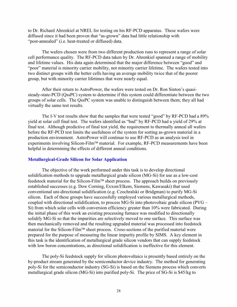
28
to Dr. Richard Ahrenkiel at NREL for testing on his RF-PCD apparatus. These wafers werediffused since it had been proven that “as-grown” data had little relationship with“post-annealed” (i.e. heat-treated or diffused) data.
The wafers chosen were from two different production runs to represent a range of solarcell performance quality. The RF-PCD data taken by Dr. Ahrenkiel spanned a range of mobilityand lifetime values. His data again determined that the major difference between “good” and“poor” material is minority carrier mobility, not minority carrier lifetime. The wafers tested intotwo distinct groups with the better cells having an average mobility twice that of the poorergroup, but with minority carrier lifetimes that were nearly equal.
After their return to AstroPower, the wafers were tested on Dr. Ron Sinton’s quasi-steady-state-PCD (QssPC) system to determine if this system could differentiate between the twogroups of solar cells. The QssPC system was unable to distinguish between them; they all hadvirtually the same test results.
The I-V test results show that the samples that were tested “good” by RF-PCD had a 89%yield at solar cell final test. The wafers identified as “bad” by RF-PCD had a yield of 29% atfinal test. Although predictive of final test yield, the requirement to thermally anneal all wafersbefore the RF-PCD test limits the usefulness of the system for sorting as-grown material in aproduction environment. AstroPower will continue to use RF-PCD as an analysis tool inexperiments involving Silicon-Film material. For example, RF-PCD measurements have beenhelpful in determining the effects of different anneal conditions.
Metallurgical-Grade Silicon for Solar Application
The objective of the work performed under this task is to develop directionalsolidification methods to upgrade metallurgical grade silicon (MG-Si) for use as a low-costfeedstock material for the Silicon-Film sheet process. The approach builds on previouslyestablished successes (e.g. Dow Corning, Exxon/Elkem, Siemens, Kawasaki) that usedconventional uni-directional solidification (e.g. Czochralski or Bridgman) to purify MG-Sisilicon. Each of these groups have successfully employed various metallurgical methods,coupled with directional solidification, to process MG-Si into photovoltaic grade silicon (PVG –Si) from which solar cells with conversion efficiency greater than 10% were fabricated. Duringthe initial phase of this work an existing processing furnace was modified to directionallysolidify MG-Si so that the impurities are selectively moved to one surface. This surface wasthen mechanically removed and the resulting upgraded material was processed into feedstockmaterial for the Silicon-Film sheet process. Cross-sections of the purified material wereprepared for the purpose of measuring the linear impurity profile by SIMS. A key element inthis task is the identification of metallurgical grade silicon vendors that can supply feedstockwith low boron concentrations, as directional solidification is ineffective for this element.
The poly-Si feedstock supply for silicon photovoltaics is presently based entirely on theby-product stream generated by the semiconductor device industry. The method for generatingpoly-Si for the semiconductor industry (SG-Si) is based on the Siemens process which convertsmetallurgical grade silicon (MG-Si) into purified poly-Si. The price of SG-Si is $45/kg to
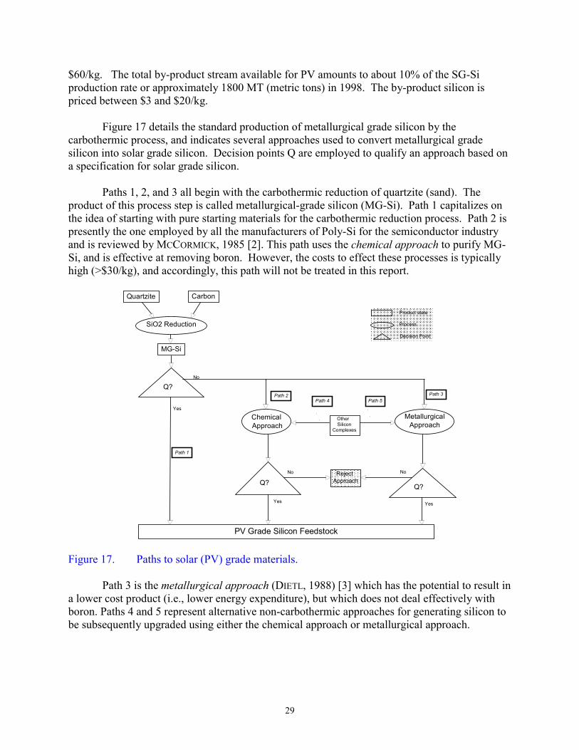
29
$60/kg. The total by-product stream available for PV amounts to about 10% of the SG-Siproduction rate or approximately 1800 MT (metric tons) in 1998. The by-product silicon ispriced between $3 and $20/kg.
Figure 17 details the standard production of metallurgical grade silicon by thecarbothermic process, and indicates several approaches used to convert metallurgical gradesilicon into solar grade silicon. Decision points Q are employed to qualify an approach based ona specification for solar grade silicon.
Paths 1, 2, and 3 all begin with the carbothermic reduction of quartzite (sand). Theproduct of this process step is called metallurgical-grade silicon (MG-Si). Path 1 capitalizes onthe idea of starting with pure starting materials for the carbothermic reduction process. Path 2 ispresently the one employed by all the manufacturers of Poly-Si for the semiconductor industryand is reviewed by MCCORMICK, 1985 [2]. This path uses the chemical approach to purify MG-Si, and is effective at removing boron. However, the costs to effect these processes is typicallyhigh (>$30/kg), and accordingly, this path will not be treated in this report.
Quartzite Carbon
SiO2 Reduction
MG-Si
Q?
Chemical Approach
MetallurgicalApproach
Q?Q?
PV Grade Silicon Feedstock
Other Silicon
Complexes
����������������������
Reject Approach
YesYes
Yes
NoNo
No
Path 1
Path 2 Path 3Path 4 Path 5
���������������������������������������������������������
Product state
Process
Decision Point
Figure 17. Paths to solar (PV) grade materials.
Path 3 is the metallurgical approach (DIETL, 1988) [3] which has the potential to result ina lower cost product (i.e., lower energy expenditure), but which does not deal effectively withboron. Paths 4 and 5 represent alternative non-carbothermic approaches for generating silicon tobe subsequently upgraded using either the chemical approach or metallurgical approach.
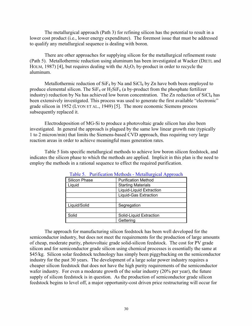
30
The metallurgical approach (Path 3) for refining silicon has the potential to result in alower cost product (i.e., lower energy expenditure). The foremost issue that must be addressedto qualify any metallurgical sequence is dealing with boron.
There are other approaches for supplying silicon for the metallurgical refinement route(Path 5). Metallothermic reduction using aluminum has been investigated at Wacker (DIETL andHOLM, 1987) [4], but requires dealing with the Al2O3 by-product in order to recycle thealuminum.
Metallothermic reduction of SiF4 by Na and SiCl4 by Zn have both been employed toproduce elemental silicon. The SiF4 or H2SiF6 (a by-product from the phosphate fertilizerindustry) reduction by Na has achieved low boron concentration. The Zn reduction of SiCl4 hasbeen extensively investigated. This process was used to generate the first available “electronic”grade silicon in 1952 (LYON ET AL., 1949) [5]. The more economic Siemens processsubsequently replaced it.
Electrodeposition of MG-Si to produce a photovoltaic grade silicon has also beeninvestigated. In general the approach is plagued by the same low linear growth rate (typically1 to 2 micron/min) that limits the Siemens-based CVD approach, thus requiring very largereaction areas in order to achieve meaningful mass generation rates.
Table 5 lists specific metallurgical methods to achieve low boron silicon feedstock, andindicates the silicon phase to which the methods are applied. Implicit in this plan is the need toemploy the methods in a rational sequence to effect the required purification.
Table 5. Purification Methods - Metallurgical ApproachSilicon Phase Purification MethodLiquid Starting Materials
Liquid-Liquid ExtractionLiquid-Gas Extraction
Liquid/Solid Segregation
Solid Solid-Liquid ExtractionGettering
The approach for manufacturing silicon feedstock has been well developed for thesemiconductor industry, but does not meet the requirements for the production of large amountsof cheap, moderate purity, photovoltaic grade solid-silicon feedstock. The cost for PV gradesilicon and for semiconductor grade silicon using chemical processes is essentially the same at$45/kg. Silicon solar feedstock technology has simply been piggybacking on the semiconductorindustry for the past 30 years. The development of a large solar power industry requires acheaper silicon feedstock that does not have the high purity requirements of the semiconductorwafer industry. For even a moderate growth of the solar industry (20% per year), the futuresupply of silicon feedstock is in question. As the production of semiconductor grade siliconfeedstock begins to level off, a major opportunity-cost driven price restructuring will occur for
31
the whole silicon feedstock industry, and the feedstock cost for silicon solar cells will increasedrastically.
The metallurgical approach shows the greatest promise for producing solar-grade silicon.A paradigm for achieving this goal is provided by the steel industry that, over the last forty years,has developed methods which employ comparable processes to produce steel with impuritycontrol at the ppm level. The necessary event is the production of a metallurgical grade siliconwith the proper boron concentration level to enable purification by subsequent metallurgicalmeans.
A key element in this task is the identification of metallurgical grade silicon vendors thatcan supply feedstock with sufficiently low boron concentrations, as directional solidification isineffective for this element. Several silicon metal vendors have provided sample material for ourproject, and discussion with industry vendors revealed potential materials that would yield boronconcentrations in the 1 ppm range. Table 6 below indicates the impurity levels of severaltargeted elements that were determined to be present in the material from these sources.
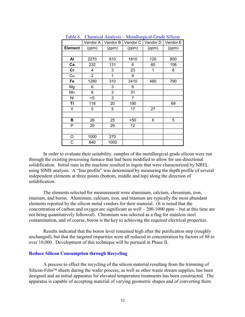
32
Table 6. Chemical Analysis – Metallurgical-Grade SiliconVendor A Vendor B Vendor C Vendor D Vendor E
Element (ppm) (ppm) (ppm) (ppm) (ppm)
Al 2270 810 1810 120 850Ca 232 131 6 60 106Cr 4 3 23 1 8
Cu 2 1 9Fe 1280 310 2410 480 790
Mg 6 3 6
Mn 8 3 31
Ni <5 3 7Ti 118 20 190 69
V 5 5 17 27
B 26 25 <50 6 5
P 29 29 12
O 1000 270
C 840 1000
In order to evaluate their suitability, samples of the metallurgical grade silicon were runthrough the existing processing furnace that had been modified to allow for uni-directionalsolidification. Initial runs in the machine resulted in ingots that were characterized by NRELusing SIMS analysis. A “line profile” was determined by measuring the depth profile of severalindependent elements at three points (bottom, middle and top) along the direction ofsolidification.
The elements selected for measurement were aluminum, calcium, chromium, iron,titanium, and boron. Aluminum, calcium, iron, and titanium are typically the most abundantelements reported by the silicon metal vendors for their material. (It is noted that theconcentration of carbon and oxygen are significant as well – 200-1000 ppm – but at this time arenot being quantitatively followed). Chromium was selected as a flag for stainless steelcontamination, and of course, boron is the key to achieving the required electrical properties.
Results indicated that the boron level remained high after the purification step (roughlyunchanged), but that the targeted impurities were all reduced in concentration by factors of 88 toover 10,000. Development of this technique will be pursued in Phase II.
Reduce Silicon Consumption through Recycling
A process to effect the recycling of the silicon material resulting from the trimming ofSilicon-Film sheets during the wafer process, as well as other waste stream supplies, has beendesigned and an initial apparatus for elevated temperature treatments has been constructed. Theapparatus is capable of accepting material of varying geometric shapes and of converting them
33
into a uniform form factor. Initially, this apparatus will produce a uniform starting material forour powder sizing process, thus enabling the achievement of higher material yield for that step.In the longer term it is anticipated that this apparatus will provide the tool for determining aprocess to convert variable size inputs to a fixed size output directly compatible with therequirements of the Silicon Film sheet machine.
Runs have verified the throughput design features intended. Material processed by theapparatus has been prepared into a Silicon-Film sheet, and has yielded solar cells of acceptableperformance. It is estimated that this and related processes will bring the material yield of as-received material through the wafer machine to over 95%.
Summary
Phase I progress for the AstroPower PVMaT-5A effort has been discussed. Significanttechnical progress has been reported in the areas of in-line wet processing, solar cell efficiencyand module cost reduction. Continuous metallization requires more development in Phases IIand III. A new high-throughput sheet machine is scheduled for fabrication in the first half of thePhase II program.
Acknowledgments
This work was supported in part by the U.S. Department of Energy through the NationalRenewable Energy Laboratory (NREL) under the Photovoltaic Manufacturing Technology(PVMaT) Program.
The authors would like to acknowledge the contributions of David Ford and EmanuelDelleDonne, Brian Atkinson, John Bisaillon, Chris Kendall, for Silicon-Film machine design,Joe Lesko for test equipment software development, and Rich Cole for manufacturing processdevelopment.
References
[1] H. Seidel, L. Csepregi, A. Heuberger, H. Baumgartel, “Anisotropic Etching of CrystallineSilicon in Alkaline Solutions”, J. Electrochemical Soc. Vol. 137, No. 11, p. 3612, Nov.1990
[2] MCCORMICK, J. R., “Polycrystalline Silicon Technology Requirements for PhotovoltaicApplications,” Silicon Processing for Photovoltaics I, Chapter 1, C. P. Khattak and C. P.Ravi, eds., Elsevier Science Publ. B. V., 1985. p. 1.
[3] DIETL J., “Metallurgical Route to Solar-Grade Silicon,” 8th E.C. PVEC, Florence, Italy(May, 1988), pp. 599-605.
[4] DIETL, J AND HOLM, C., Technical Digest of the International PVSEC-3, Tokyo, Japan(November, 1987) pp.533-536.
[5] LYON, D. W., OLSEN, C. M. AND LEWIS, E. D., Journal of the Electrochemical Society,Vol. 96, No. 6, 359-363 (1949).
REPORT DOCUMENTATION PAGE Form ApprovedOMB NO. 0704-0188
Public reporting burden for this collection of information is estimated to average 1 hour per response, including the time for reviewing instructions, searching existing datasources, gathering and maintaining the data needed, and completing and reviewing the collection of information. Send comments regarding this burden estimate or any otheraspect of this collection of information, including suggestions for reducing this burden, to Washington Headquarters Services, Directorate for Information Operations andReports, 1215 Jefferson Davis Highway, Suite 1204, Arlington, VA 22202-4302, and to the Office of Management and Budget, Paperwork Reduction Project (0704-0188),Washington, DC 20503.
1. AGENCY USE ONLY (Leave blank) 2. REPORT DATESeptember 1999
3. REPORT TYPE AND DATES COVERED
Annual Subcontract Report, 16 April 1998 – 31 January 19994. TITLE AND SUBTITLE
Silicon-Film™ Solar Cells by a Flexible Manufacturing System6. AUTHOR(S)
J.S. Culik, J.A. Rand, Y. Bai, J.R. Bower, J.R. Cummings, I. Goncharovsky, R. Jonczyk, P.E. Sims,R.B. Hall, and A.M. Barnett
5. FUNDING NUMBERS
C: ZAX-8-17647-1TA: PV906101
7. PERFORMING ORGANIZATION NAME(S) AND ADDRESS(ES)
AstroPower, Inc.Solar ParkNewark, DE 19716
8. PERFORMING ORGANIZATIONREPORT NUMBER
9. SPONSORING/MONITORING AGENCY NAME(S) AND ADDRESS(ES)
National Renewable Energy Laboratory1617 Cole Blvd.Golden, CO 80401-3393
10. SPONSORING/MONITORINGAGENCY REPORT NUMBER
SR-520-26834
11. SUPPLEMENTARY NOTES
NREL Technical Monitor: R.L. Mitchell
12a. DISTRIBUTION/AVAILABILITY STATEMENT
National Technical Information ServiceU.S. Department of Commerce5285 Port Royal RoadSpringfield, VA 22161
12b. DISTRIBUTION CODE
13. ABSTRACT (Maximum 200 words)
AstroPower is developing a manufacturing process for Silicon-Film™ solar cell production under the Photovoltaic ManufacturingTechnology (PVMaT) cost-share program. This document reports on results from the first phase of a three-phase effort. Progress isreported on developing new procedures and equipment for in-line wet-chemical processes, metallization processes, sheet fabrication, solarcell processing, module assembly, solar cell testing, metallurgical-grade silicon purification, and recycling of Silicon-Film™ sheetmaterials. Future concepts and goals for the Silicon-Film™ process are also discussed.
15. NUMBER OF PAGES 14. SUBJECT TERMS
photovoltaics ; Photovoltaic Manufacturing Technology ; PVMaT ; Silicon-Film™ ; in-line wetprocessing ; continuous metallization ; solar cell efficiency ; module cost reduction ;manufacturing system
16. PRICE CODE
17. SECURITY CLASSIFICATIONOF REPORTUnclassified
18. SECURITYCLASSIFICATIONOF THIS PAGEUnclassified
19. SECURITY CLASSIFICATIONOF ABSTRACTUnclassified
20. LIMITATION OF ABSTRACT
UL
NSN 7540-01-280-5500 Standard Form 298 (Rev. 2-89)Prescribed by ANSI Std. Z39-18
298-102