Embed Size (px)
Citation preview
SiGe-based Power Amplifier for CDMA Handset Circuitry
Ping Chen, Weixin Li
SiGe-based Power Amplifier in RF and Microwave Circuit
OutlineOutline
Introduction
Literature review and discussionLiterature review and discussion
Device design and performance
Circuit design and performance Circuit design and performance
Commercial application
C l i Conclusion
SiGe-based Power Amplifier in RF and Microwave Circuit
IntroductionIntroduction
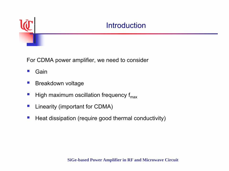
For CDMA power amplifier, we need to consider
GainGain
Breakdown voltage
High maximum oscillation frequency fmaxg q y max
Linearity (important for CDMA)
Heat dissipation (require good thermal conductivity)
SiGe-based Power Amplifier in RF and Microwave Circuit
IntroductionIntroduction
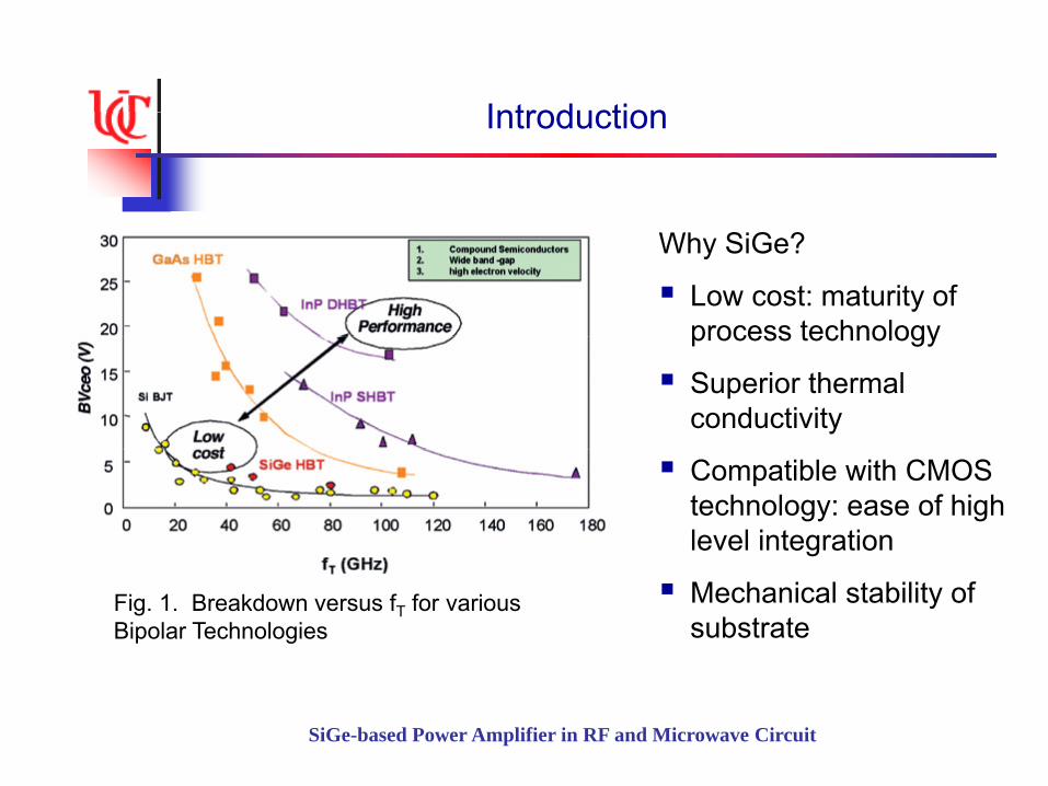
Why SiGe?
Low cost: maturity of process technologyprocess technology
Superior thermal conductivity
Compatible with CMOS technology: ease of high level integration
Fig. 1. Breakdown versus fT for various Bipolar Technologies
Mechanical stability of substrate
SiGe-based Power Amplifier in RF and Microwave Circuit
IntroductionIntroduction
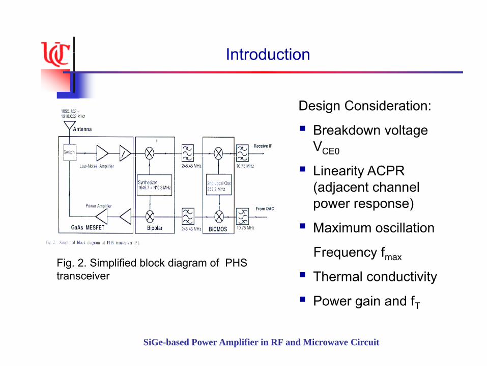
Design Consideration:Design Consideration:
Breakdown voltage VCE0
Linearity ACPR (adjacent channel power response)
Fig 2 Simplified block diagram of PHS
p p )
Maximum oscillation
Frequency fmaxFig. 2. Simplified block diagram of PHStransceiver Thermal conductivity
Power gain and fT
SiGe-based Power Amplifier in RF and Microwave Circuit
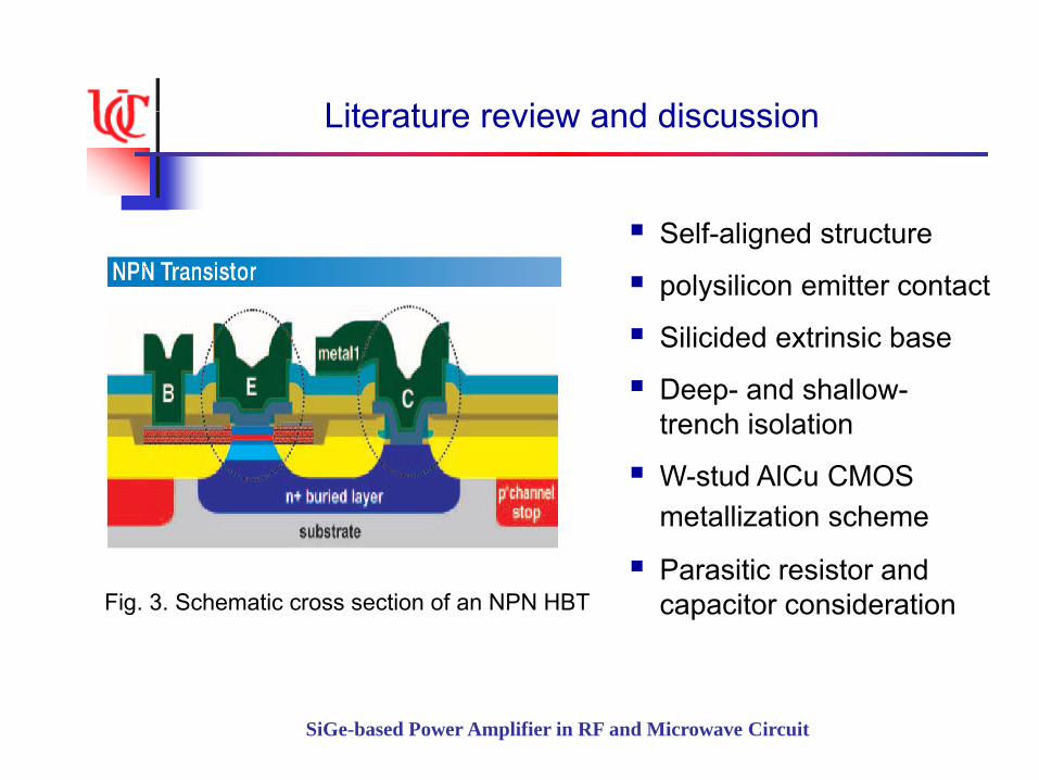
Literature review and discussionLiterature review and discussion
S lf li d Self-aligned structure
polysilicon emitter contact
Silicided extrinsic base Silicided extrinsic base
Deep- and shallow-trench isolation
W-stud AlCu CMOS metallization scheme
Fig. 3. Schematic cross section of an NPN HBT Parasitic resistor and
capacitor consideration
SiGe-based Power Amplifier in RF and Microwave Circuit
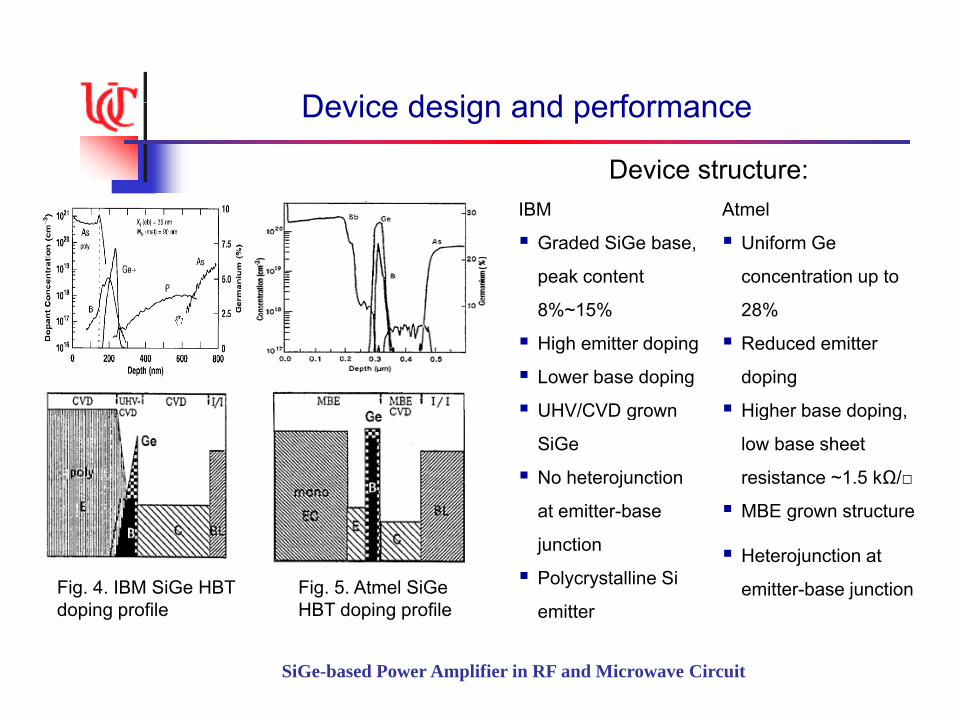
Device design and performanceDevice design and performance
IBM At l
Device structure:IBM
Graded SiGe base,
peak content
8% 15%
Atmel
Uniform Ge
concentration up to
28%8%~15%
High emitter doping
Lower base doping
UHV/CVD grown
28%
Reduced emitter
doping
Higher base doping UHV/CVD grown
SiGe
No heterojunction
at emitter-base
Higher base doping,
low base sheet
resistance ~1.5 kΩ/
MBE grown structure
Fig. 4. IBM SiGe HBT doping profile
Fig. 5. Atmel SiGe HBT doping profile
at emitter-base
junction
Polycrystalline Si
emitter
MBE grown structure
Heterojunction at
emitter-base junction
SiGe-based Power Amplifier in RF and Microwave Circuit
doping profile HBT doping profile emitter
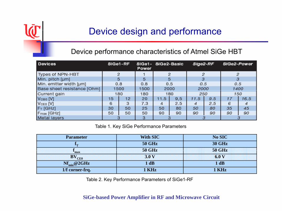
Device design and performanceDevice design and performance
Device performance characteristics of Atmel SiGe HBT
Table 1. Key SiGe Performance Parameters
Parameter With SIC No SICfT 50 GHz 30 GHz
f 50 GHz 50 GHzfmax 50 GHz 50 GHzBVCE0 3.0 V 6.0 V
Nfmin@2GHz 1 dB 1 dB1/f corner-frq. 1 KHz 1 KHz
Table 2. Key Performance Parameters of SiGe1-RF
SiGe-based Power Amplifier in RF and Microwave Circuit
Table 2. Key Performance Parameters of SiGe1 RF
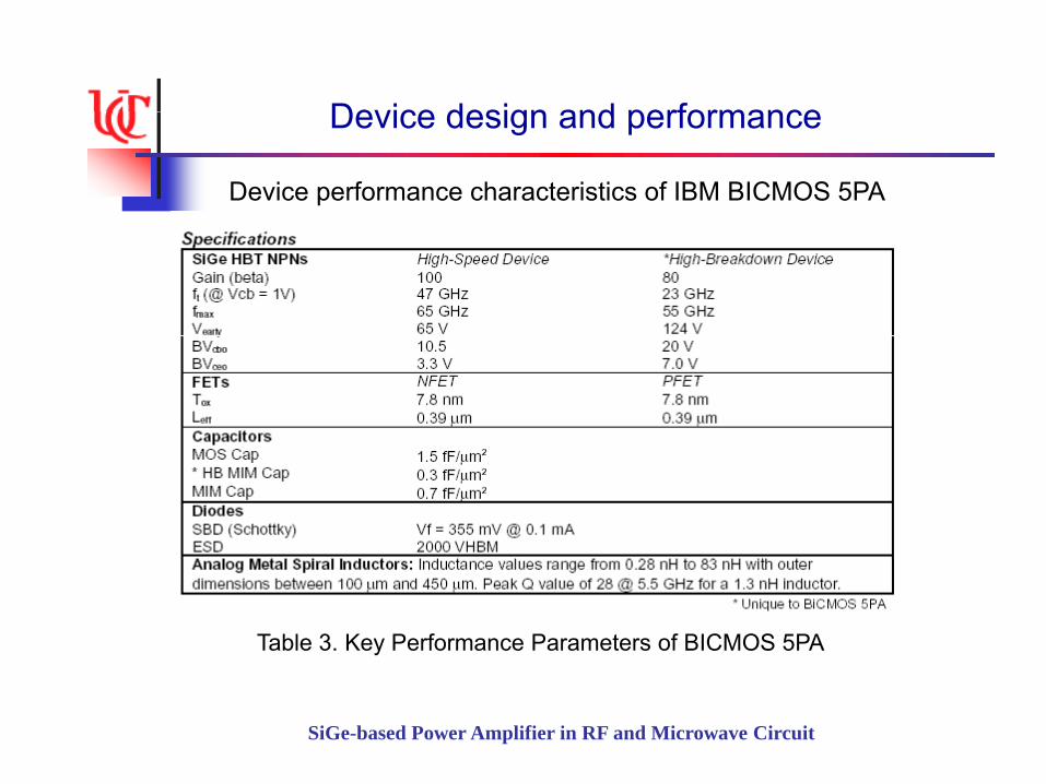
Device design and performanceDevice design and performance
Device performance characteristics of IBM BICMOS 5PA
Table 3. Key Performance Parameters of BICMOS 5PA
SiGe-based Power Amplifier in RF and Microwave Circuit
Device design and performanceDevice design and performance
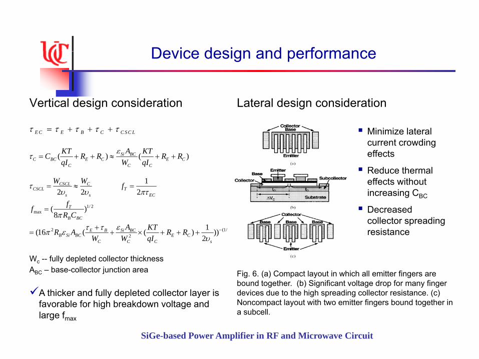
Vertical design consideration Lateral design considerationVertical design consideration
E C E B C C SC L
Lateral design consideration
( ) ( )Si BCAKT KTC R R R R
Minimize lateral current crowding effects( ) ( )Si BC
C BC E C E CC C C
C R R R RqI W qI
2 2CSCL C
CSCLs s
W W
1
2TEC
f
1/ 2f
effects
Reduce thermal effects without increasing CBC
1/ 2max
2 (1/ 2)2
( )8
1(16 ( ( ) ))2
T
B BC
Si BCE BB Si BC E C
C C C s
ffR C
A KTR A R RW W qI
W f ll d l t d ll t thi k
Decreased collector spreading resistance
Wc -- fully depleted collector thicknessABC – base-collector junction area
A thicker and fully depleted collector layer is favorable for high breakdown voltage and
Fig. 6. (a) Compact layout in which all emitter fingers are bound together. (b) Significant voltage drop for many finger devices due to the high spreading collector resistance. (c) Noncompact layout with two emitter fingers bound together in
SiGe-based Power Amplifier in RF and Microwave Circuit
g glarge fmax
a subcell.
Circuit design and performanceCircuit design and performance
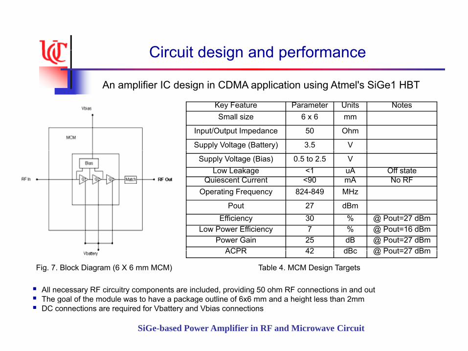
An amplifier IC design in CDMA application using Atmel's SiGe1 HBT
Key Feature Parameter Units NotesSmall size 6 x 6 mm
Input/Output Impedance 50 Ohm
Supply Voltage (Battery) 3.5 V
Supply Voltage (Bias) 0.5 to 2.5 VLow Leakage <1 uA Off state
Quiescent Current <90 mA No RFOperating Frequency 824-849 MHz
Pout 27 dBmEfficiency 30 % @ Pout=27 dBm
Low Power Efficiency 7 % @ Pout=16 dBmPower Gain 25 dB @ Pout=27 dBm
ACPR 42 dBc @ Pout=27 dBm
Fig. 7. Block Diagram (6 X 6 mm MCM)
ACPR 42 dBc @ Pout=27 dBm
Table 4. MCM Design Targets
All necessary RF circuitry components are included, providing 50 ohm RF connections in and out The goal of the module was to have a package outline of 6x6 mm and a height less than 2mm
SiGe-based Power Amplifier in RF and Microwave Circuit
The goal of the module was to have a package outline of 6x6 mm and a height less than 2mm DC connections are required for Vbattery and Vbias connections
Circuit design and performanceCircuit design and performance
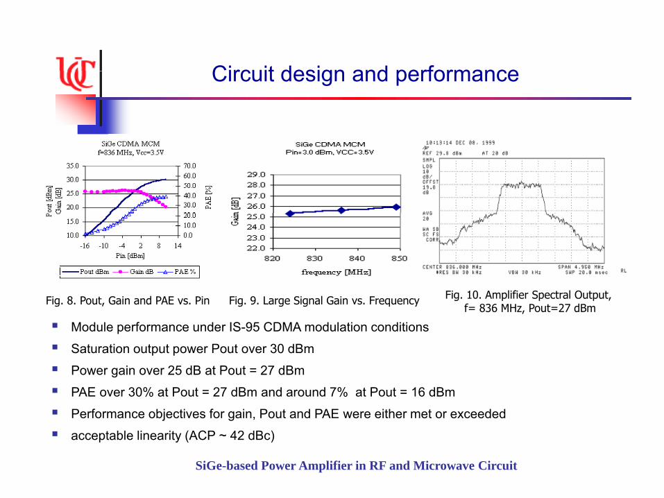
Fig. 8. Pout, Gain and PAE vs. Pin Fig. 9. Large Signal Gain vs. Frequency Fig. 10. Amplifier Spectral Output,f= 836 MHz, Pout=27 dBm
Module performance under IS-95 CDMA modulation conditions
Saturation output power Pout over 30 dBmp p
Power gain over 25 dB at Pout = 27 dBm
PAE over 30% at Pout = 27 dBm and around 7% at Pout = 16 dBm
Performance objectives for gain, Pout and PAE were either met or exceeded
SiGe-based Power Amplifier in RF and Microwave Circuit
acceptable linearity (ACP ~ 42 dBc)
Circuit design and performanceCircuit design and performance
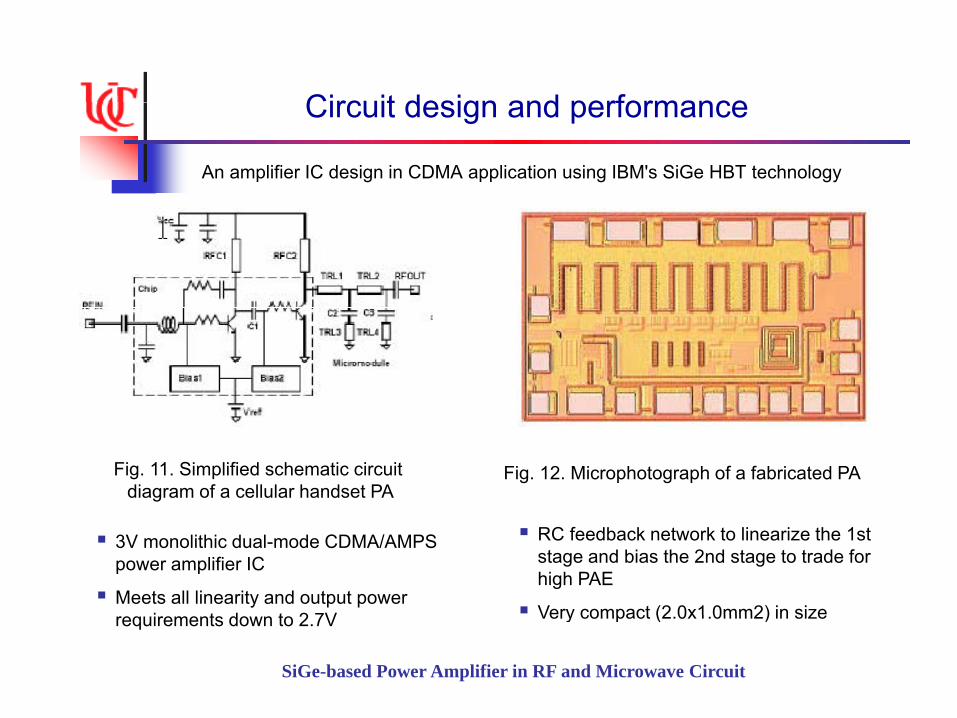
An amplifier IC design in CDMA application using IBM's SiGe HBT technology
Fig. 11. Simplified schematic circuit diagram of a cellular handset PA
Fig. 12. Microphotograph of a fabricated PA
3V monolithic dual-mode CDMA/AMPS power amplifier IC
Meets all linearity and output power i t d t 2 7V
RC feedback network to linearize the 1st stage and bias the 2nd stage to trade for high PAE
Very compact (2 0x1 0mm2) in size
SiGe-based Power Amplifier in RF and Microwave Circuit
requirements down to 2.7V Very compact (2.0x1.0mm2) in size
Circuit design and performanceCircuit design and performance
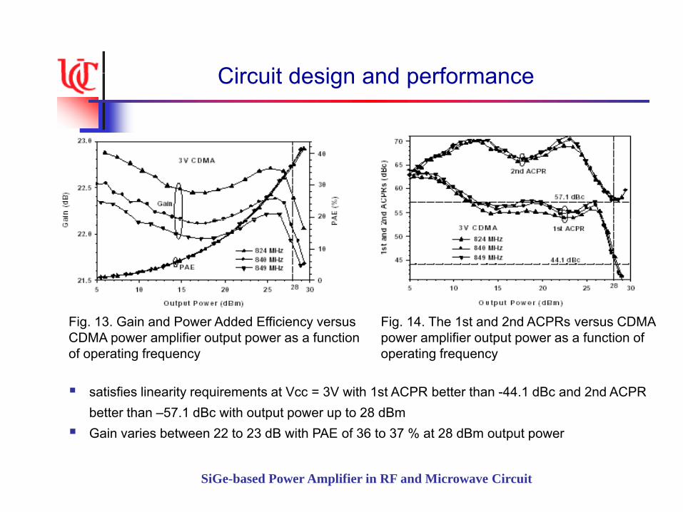
Fig. 13. Gain and Power Added Efficiency versusCDMA power amplifier output power as a functionof operating frequency
Fig. 14. The 1st and 2nd ACPRs versus CDMApower amplifier output power as a function of operating frequency
satisfies linearity requirements at Vcc = 3V with 1st ACPR better than -44.1 dBc and 2nd ACPR better than –57.1 dBc with output power up to 28 dBm
Gain varies between 22 to 23 dB with PAE of 36 to 37 % at 28 dBm output power
SiGe-based Power Amplifier in RF and Microwave Circuit
p p
Circuit design and performanceCircuit design and performance
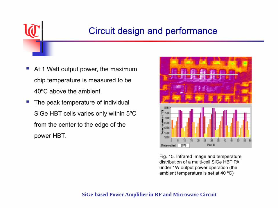
At 1 Watt output power, the maximum
chip temperature is measured to be
40ºC b th bi t40ºC above the ambient.
The peak temperature of individual
SiGe HBT cells varies only within 5ºC
from the center to the edge of the
power HBT.
Fig. 15. Infrared Image and temperature distribution of a multi-cell SiGe HBT PA under 1W output power operation (the ambient temperature is set at 40 ºC)
SiGe-based Power Amplifier in RF and Microwave Circuit
Commercial applicationCommercial application
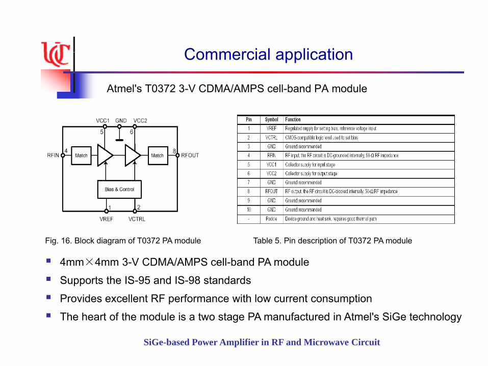
Atmel's T0372 3-V CDMA/AMPS cell-band PA module
Fig. 16. Block diagram of T0372 PA module Table 5. Pin description of T0372 PA module
4mm×4mm 3 V CDMA/AMPS cell band PA module 4mm×4mm 3-V CDMA/AMPS cell-band PA module
Supports the IS-95 and IS-98 standards
Provides excellent RF performance with low current consumption
Th h t f th d l i t t PA f t d i At l' SiG t h l
SiGe-based Power Amplifier in RF and Microwave Circuit
The heart of the module is a two stage PA manufactured in Atmel's SiGe technology
Commercial applicationCommercial application
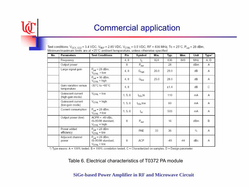
Table 6 Electrical characteristics of T0372 PA module
SiGe-based Power Amplifier in RF and Microwave Circuit
Table 6. Electrical characteristics of T0372 PA module
Commercial applicationCommercial application
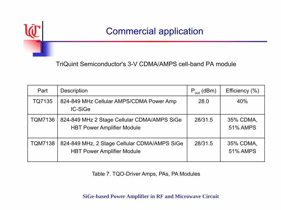
TriQuint Semiconductor's 3-V CDMA/AMPS cell-band PA module
Part Description P (dBm) Efficiency (%)Part Description Pout (dBm) Efficiency (%)
TQ7135 824-849 MHz Cellular AMPS/CDMA Power Amp IC-SiGe
28.0 40%
TQM7136 824-849 MHz 2 Stage Cellular CDMA/AMPS SiGe 28/31 5 35% CDMATQM7136 824-849 MHz 2 Stage Cellular CDMA/AMPS SiGe HBT Power Amplifier Module
28/31.5 35% CDMA,51% AMPS
TQM7138 824-849 MHz, 2 Stage Cellular CDMA/AMPS SiGe HBT P A lifi M d l
28/31.5 35% CDMA,51% AMPSHBT Power Amplifier Module 51% AMPS
Table 7. TQO-Driver Amps, PAs, PA Modules
SiGe-based Power Amplifier in RF and Microwave Circuit
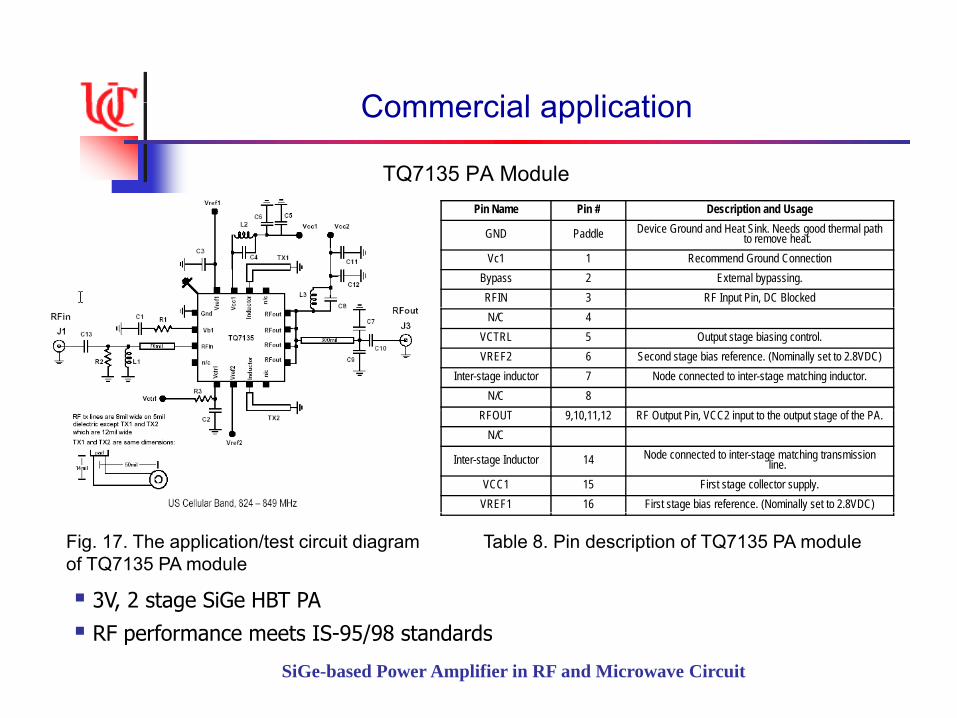
Commercial applicationCommercial application
TQ7135 PA ModulePi N Pi # D i ti d UPin Name Pin # Description and Usage
GND Paddle Device Ground and Heat Sink. Needs good thermal path to remove heat.
Vc1 1 Recommend Ground ConnectionBypass 2 External bypassing.RFIN 3 RF Input Pin, DC BlockedN/C 4
VCTRL 5 Output stage biasing control.VREF2 6 Second stage bias reference. (Nominally set to 2.8VDC)
Inter-stage inductor 7 Node connected to inter-stage matching inductor.N/C 8
RFOUT 9,10,11,12 RF Output Pin, VCC2 input to the output stage of the PA.N/C
Inter-stage Inductor 14 Node connected to inter-stage matching transmission line.
VCC1 15 First stage collector supply.VREF1 16 First stage bias reference. (Nominally set to 2.8VDC)
Fig. 17. The application/test circuit diagram of TQ7135 PA module
Table 8. Pin description of TQ7135 PA module
3V, 2 stage SiGe HBT PA
SiGe-based Power Amplifier in RF and Microwave Circuit
RF performance meets IS-95/98 standards
Commercial applicationCommercial application
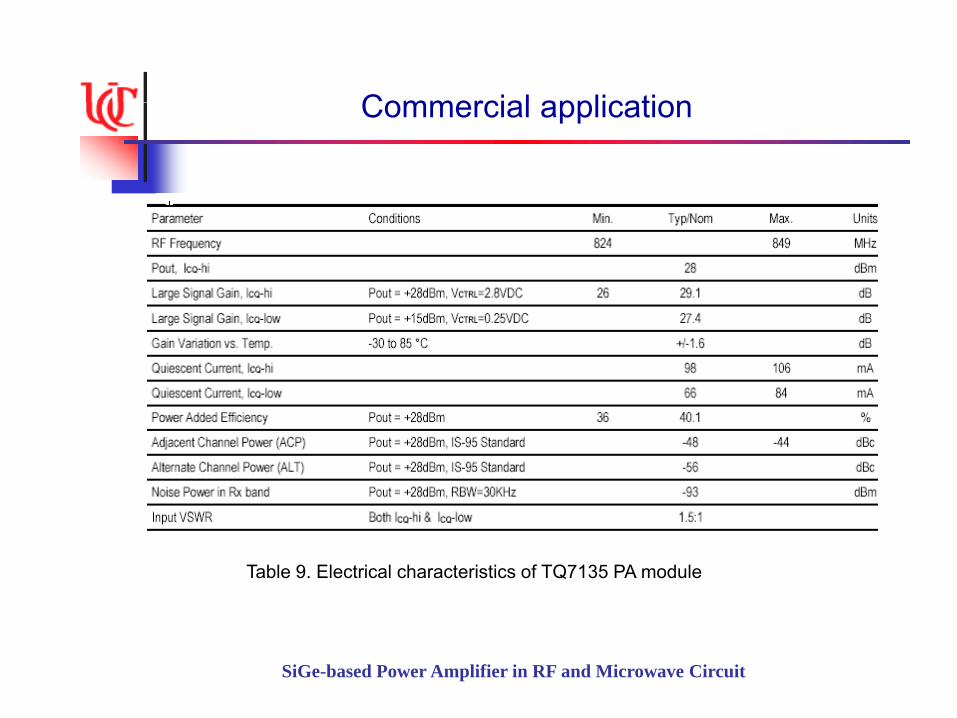
Table 9. Electrical characteristics of TQ7135 PA module
SiGe-based Power Amplifier in RF and Microwave Circuit
Commercial applicationCommercial application
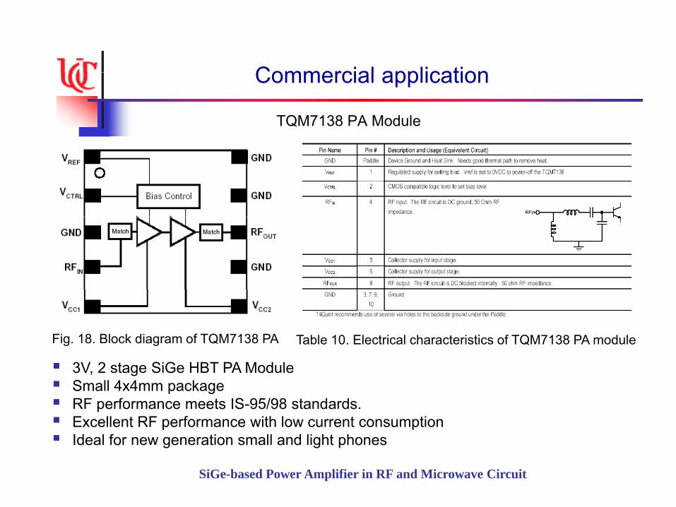
TQM7138 PA Module
Fig. 18. Block diagram of TQM7138 PA Table 10. Electrical characteristics of TQM7138 PA module
S G 3V, 2 stage SiGe HBT PA Module Small 4x4mm package RF performance meets IS-95/98 standards. Excellent RF performance with low current consumption
Id l f i ll d li h h
SiGe-based Power Amplifier in RF and Microwave Circuit
Ideal for new generation small and light phones
Commercial applicationCommercial application
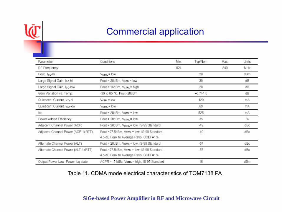
Table 11. CDMA mode electrical characteristics of TQM7138 PA
SiGe-based Power Amplifier in RF and Microwave Circuit
Commercial applicationCommercial application
IBM developed SiGe-base PA in wireless communication application in 2002
Three SiGe PA modules: IBM 2022, IBM 2018, and IBM 2017Three SiGe PA modules: IBM 2022, IBM 2018, and IBM 2017
0.5-μm process
The 2018 PA is designed for US CDMA/AMPS designs. In CDMA mode, it
features +28.5 dBm output power 35% power added efficiency (PAE). sports on-chip VSWR protection, a less than 1μA standby current 6 x 6-mm package.
SiGe-based Power Amplifier in RF and Microwave Circuit
ConclusionsConclusions
1. SiGe HBT technology combines transistor performance competitive
with III–V technologies with the processing maturity, integration
levels yield and cost It has emerged from the research laboratorylevels, yield, and cost. It has emerged from the research laboratory,
entered manufacturing on 200-mm wafers, and is ready commercial
RF and microwave market.
2. Power HBT design targeting high breakdown voltage with low
current density can be obtained by designing a thick and lightly
doped collector laye. A multifinger emitter configuration is required
for high current density to reduce thermal effects
SiGe-based Power Amplifier in RF and Microwave Circuit
ConclusionsConclusions
3. Specially designed SiGe HBTs used in CDMA handset PAs can have a breakdown
voltage BVCE0 as high as 7.3 Vand 7 V, fmax of 50 GHz and 55 GHz , current gain of 180
and 80 for Atmel SiGe technology and IBM SiGe technology respectivelyand 80 for Atmel SiGe technology and IBM SiGe technology respectively
4. Commercially available SiGe based CDMA PAs can have an output power of 28 dBm,
and power PAE over 35%. The acceptable linearity for specially designed circuitry can be
as low as ACP~ 42dBcas low as ACP~ 42dBc
5. Future SiGe PA designs should target linearity improvement at higher power levels
typically required in today's handsets. Ongoing development efforts by the semiconductor
i d t h ld ti t i d i bilit d f l l f SiGindustry should continue to improve device capability and performance levels of SiGe
leading to it's increased use and new opportunities in RF analog products
SiGe-based Power Amplifier in RF and Microwave Circuit
End of slide
SiGe-based Power Amplifier in RF and Microwave Circuit