Embed Size (px)
Citation preview
Rev 09 716 Copyright copy 2016 by Silicon Labs Si5341-D-EVB
Si5341-D-EVB
Si5341-D EVALUATION BOARD USERrsquoS GUIDE
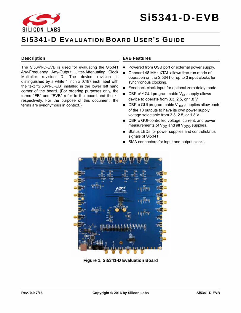
Description
The Si5341-D-EVB is used for evaluating the Si5341Any-Frequency Any-Output Jitter-Attenuating ClockMultiplier revision D The device revision isdistinguished by a white 1 inch x 0187 inch label withthe text ldquoSI5341-D-EBrdquo installed in the lower left handcorner of the board (For ordering purposes only theterms ldquoEBrdquo and ldquoEVBrdquo refer to the board and the kitrespectively For the purpose of this document theterms are synonymous in context)
EVB Features
Powered from USB port or external power supply
Onboard 48 MHz XTAL allows free-run mode of operation on the Si5341 or up to 3 input clocks for synchronous clocking
Feedback clock input for optional zero delay mode
CBPro GUI programmable VDD supply allows device to operate from 33 25 or 18 V
CBPro GUI programmable VDDO supplies allow each of the 10 outputs to have its own power supply voltage selectable from 33 25 or 18 V
CBPro GUI-controlled voltage current and power measurements of VDD and all VDDO supplies
Status LEDs for power supplies and controlstatus signals of Si5341
SMA connectors for input and output clocks
Figure 1 Si5341-D Evaluation Board
Si5341-D-EVB
2 Rev 09
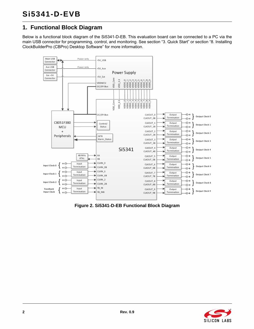
1 Functional Block DiagramBelow is a functional block diagram of the Si5341-D-EB This evaluation board can be connected to a PC via themain USB connector for programming control and monitoring See section ldquo3 Quick Startrdquo or section ldquo8 InstallingClockBuilderPro (CBPro) Desktop Softwarerdquo for more information
Figure 2 Si5341-D-EB Functional Block Diagram
Si5341-D-EVB
Rev 09 3
2 Si5341-D-EVB Support Documentation and ClockBuilderPro SoftwareAll Si5341-D-EVB schematics BOMs Userrsquos Guides and software can be found online at the following link
httpwwwsilabscomproductsclocksoscillatorspagessi538x-4x-evbaspx
3 Quick Start1 Install ClockBuilderPro desktop software from httpwwwsilabscomCBPro
2 Connect a USB cable from Si5341-D-EB to the PC where the software was installed
3 Leave the jumpers as installed from the factory and launch the ClockBuilderPro software
4 You can use ClockBuilderPro to create download and run a frequency plan on the Si5341-D-EB
5 For the Si5341 data sheet go to httpwwwsilabscomtiming
Si5341-D-EVB
4 Rev 09
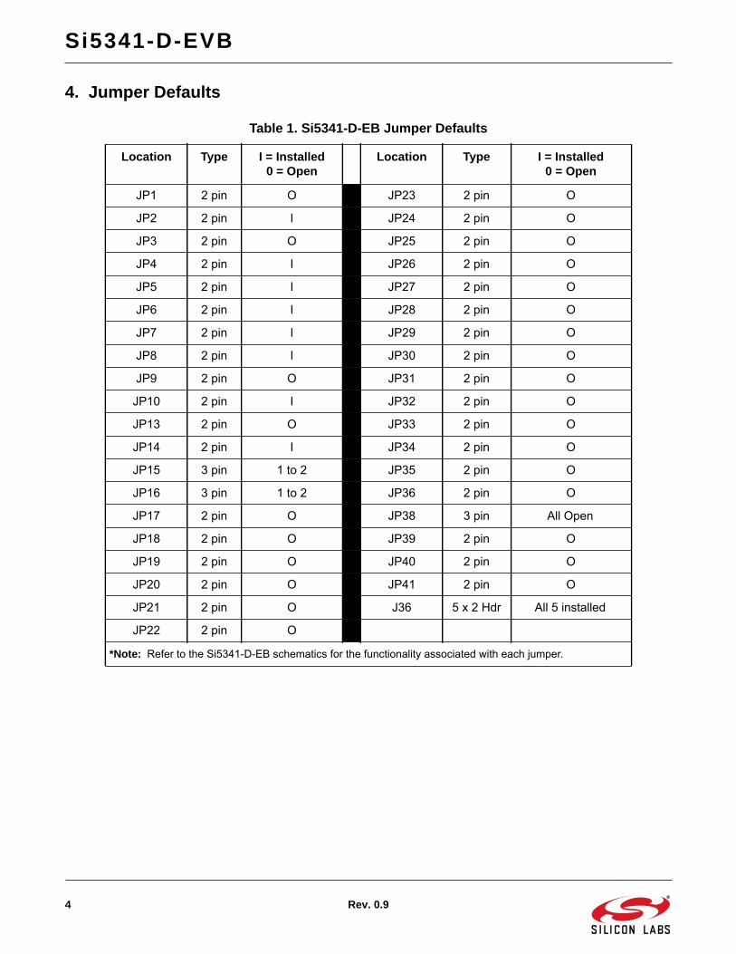
4 Jumper Defaults
Table 1 Si5341-D-EB Jumper Defaults
Location Type I = Installed0 = Open
Location Type I = Installed0 = Open
JP1 2 pin O JP23 2 pin O
JP2 2 pin I JP24 2 pin O
JP3 2 pin O JP25 2 pin O
JP4 2 pin I JP26 2 pin O
JP5 2 pin I JP27 2 pin O
JP6 2 pin I JP28 2 pin O
JP7 2 pin I JP29 2 pin O
JP8 2 pin I JP30 2 pin O
JP9 2 pin O JP31 2 pin O
JP10 2 pin I JP32 2 pin O
JP13 2 pin O JP33 2 pin O
JP14 2 pin I JP34 2 pin O
JP15 3 pin 1 to 2 JP35 2 pin O
JP16 3 pin 1 to 2 JP36 2 pin O
JP17 2 pin O JP38 3 pin All Open
JP18 2 pin O JP39 2 pin O
JP19 2 pin O JP40 2 pin O
JP20 2 pin O JP41 2 pin O
JP21 2 pin O J36 5 x 2 Hdr All 5 installed
JP22 2 pin O
Note Refer to the Si5341-D-EB schematics for the functionality associated with each jumper
Si5341-D-EVB
Rev 09 5
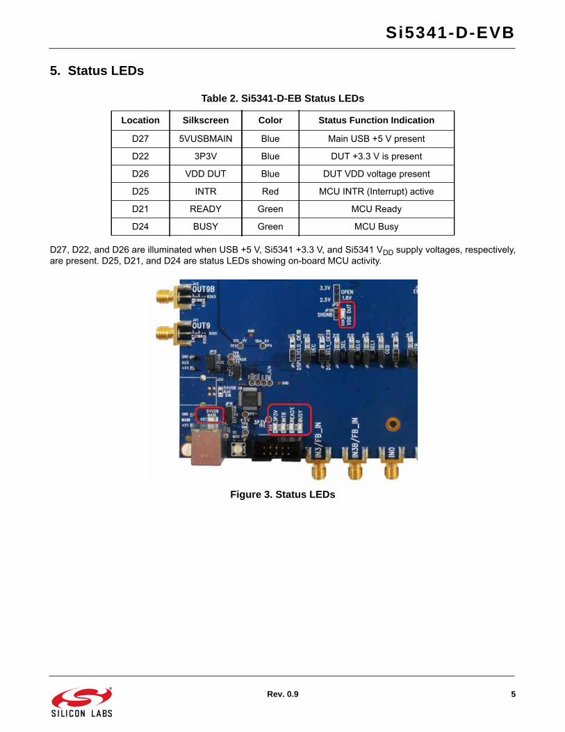
5 Status LEDs
D27 D22 and D26 are illuminated when USB +5 V Si5341 +33 V and Si5341 VDD supply voltages respectivelyare present D25 D21 and D24 are status LEDs showing on-board MCU activity
Figure 3 Status LEDs
Table 2 Si5341-D-EB Status LEDs
Location Silkscreen Color Status Function Indication
D27 5VUSBMAIN Blue Main USB +5 V present
D22 3P3V Blue DUT +33 V is present
D26 VDD DUT Blue DUT VDD voltage present
D25 INTR Red MCU INTR (Interrupt) active
D21 READY Green MCU Ready
D24 BUSY Green MCU Busy
Si5341-D-EVB
6 Rev 09
6 Clock Input Circuits (INxINxB and FB_INFB_INB)The Si5341-D-EB has eight SMA connectors (IN0IN0BndashIN2IN3B and FB_INFB_INB) for receiving external clocksignals All input clocks are terminated as shown in Figure 4 below Note input clocks are ac-coupled and 50 terminated This represents four differential input clock pairs Single-ended clocks can be used by appropriatelydriving one side of the differential pair with a single-ended clock For details on how to configure inputs assingle-ended please refer to the Si5341 data sheet
Figure 4 Input Clock Termination Circuit
7 Clock Output Circuits (OUTxOUTxB)Each of the twenty output drivers (10 differential pairs) is ac-coupled to its respective SMA connector The outputclock termination circuit is shown in Figure 5 below The output signal will have no dc bias If dc coupling isrequired the ac coupling capacitors can be replaced with a resistor of appropriate value The Si5341-D-EVBprovides pads for optional output termination resistors andor low frequency capacitors Note that components withschematic ldquoNIrdquo designation are not normally populated on the Si5341-D-EB and provide locations on the PCB foroptional dcac terminations by the end user
Figure 5 Output Clock Termination Circuit
Si5341-D-EVB
Rev 09 7
8 Installing ClockBuilderPro (CBPro) Desktop SoftwareTo install the CBOPro software on any Windows 7 (or above) PC
Go to httpwwwsilabscomCBPro and download ClockBuilderPro software
Installation instructions and Userrsquos Guide for ClockBuilderPro can be found at the download link shown abovePlease follow the instructions as indicated
9 Using the Si5341-D-EVB91 Connecting the EVB to Your Host PCOnce ClockBuilderPro software is installed connect to the evaluation board with a USB cable as shown below
Figure 6 EVB Connection Diagram
Si5341-D-EVB
8 Rev 09
92 Additional Power SuppliesAlthough additional power (besides the power supplied by the host PCrsquos USB port) is not needed for mostconfigurations two additional +5 VDC power supplies (MAIN and AUX) can be connected to J33 and J34 (locatedon the bottom of the board near the USB connector) Refer to the Si5341-D-EB schematic for details
The Si5341-EB comes preconfigured with jumpers installed at JP15 and JP16 (pins 1-2 in both cases) in order toselect ldquoUSBrdquo These jumpers together with the components installed configure the evaluation board to obtain all+5 V power solely through the main USB connector at J37 This setup is the default configuration and shouldnormally be sufficient
Figure 7 shows the correct installation of the jumper shunts at JP15 and JP16 for default or standard operation
Figure 7 JP15-JP16 Standard Jumper Shunt InstallationErrata NoteSome early versions of the 64-pin Si534x-EBs may have the silkscreen text at JP15-JP16 reversed regarding EXT
and USB ie USB EXT instead of EXT USB Regardless the correct installation of the jumper shunts for defaultor standard operation is on the right hand side as read and viewed in Figure 7
The general guidelines for single USB power supply operation are listed below
Use either a USB 30 or USB 20 port These ports are specified to supply 900 mA and 500 mA respectively at +5 V
If you are working with a USB 20 port and you are current limited turn off enough DUT output voltage regulators to drop the total DUT current le 470 mA (Note USB 20 ports may supply gt 500 mA Provided the nominal +5 V drops gracefully by less than 10 the EVB will still work)
If you are working with a USB 20 and you are current limited and need all output clock drivers enabled re-configure the EB to drive the DUT output voltage regulators from an external +5 V power supply as follows
Connect external +5 V power supply to terminal block J33 on the back side of the PCBMove the jumper at JP15 from pins 1-2 USB to pins 2-3 EXT
Si5341-D-EVB
Rev 09 9
93 Overview of ClockBuilderPro ApplicationsNote The following instructions and screen captures may vary slightly depending on your version of ClockBuilderPro The ClockBuilderPro installer will install two main applications
Figure 8 Application 1 ClockbuilderPro WizardUse the CBPro Wizard to
Create a new design
Review or edit an existing design
Export create in-system programming
Figure 9 Application 2 EVB GUIUse the EVB GUI to
Download configuration to EVBrsquos DUT (Si5341)
Control the EVBrsquos regulators
Monitor voltage current power on the EVB
Si5341-D-EVB
10 Rev 09
94 Common ClockBuilderPro Work Flow ScenariosThere are three common workflow scenarios when using CBPro and the Si5341-D-EVB These workflow scenariosare
Workflow Scenario 1 Testing a Silicon Labs-Created Default Configuration
Workflow Scenario 2 Modifying the Default Silicon Labs-Created Device Configuration
Workflow Scenario 3 Testing a User-Created Device Configuration
Each is described in more detail in the following sections
95 Workflow Scenario 1 Testing a Silicon Labs-Created Default ConfigurationThe flow for using the EVB GUI to initialize and control a device on the EVB is as follows
Once the PC and EVB are connected launch ClockBuilder Pro by clicking on this icon on your PCrsquos desktop
Figure 10 ClockBuilderPro Desktop IconIf an EVB is detected click on the ldquoOpen Default Planrdquo button on the Wizardrsquos main menu CBPro automaticallydetects the EVB and device type
Figure 11 Open Default PlanOnce you open the default plan (based on your EVB model number) a popup will appear
Figure 12 Write Design to EVB DialogSelect ldquoYesrdquo to write the default plan to the Si5341 device mounted on your EVB This ensures the device iscompletely reconfigured per the Silicon Labs default plan for the DUT type mounted on the EVB
Si5341-D-EVB
Rev 09 11
Figure 13 Writing Design StatusAfter CBPro writes the default plan to the EVB click on ldquoOpen EVB GUIrdquo as shown below
Figure 14 Open EVB GUIThe EVB GUI will appear Note all power supplies will be set to the values defined in the devicersquos default CBProproject file created by Silicon Labs as shown below
Figure 15 EVB GUI Window
Si5341-D-EVB
12 Rev 09
951 Verify Free-Run Mode OperationAssuming no external clocks have been connected to the INPUT CLOCK differential SMA connectors (labeledldquoINxINxBrdquo) located around the perimeter of the EVB the DUT should now be operating in free-run mode as theDUT will be locked to the crystal in this case
You can run a quick check to determine if the device is powered up and generating output clocks (and consumingpower) by clicking on the Read All button highlighted above and then reviewing the voltage current and powerreadings for each VDDx supply
Note Shutting ldquoOffrdquo then ldquoOnrdquo of the VDD and VDDA supplies will power-down and reset the DUT Every time you dothis to reload the Silicon Labs-created default plan into the DUTrsquos register space you must go back to the Wiz-ardrsquos main menu and select ldquoWrite Design to EVBrdquo
Figure 16 Write Design to EVBFailure to do the step above will cause the device to read in a pre-programmed plan from its non-volatilememory (NVM) However the plan loaded from the NVM may not be the latest plan recommended bySilicon Labs for evaluationAt this point you should verify the presence and frequencies of the output clocks (running to free-run mode fromthe crystal) using appropriate external instrumentation connected to the output clock SMA connectors To verify theoutput clocks are toggling at the correct frequency and signal format click on View Design Report as highlightedbelow
Figure 17 View Design Report
Si5341-D-EVB
Rev 09 13
Your configurationrsquos design report will appear in a new window as shown below Compare the observed outputclocks to the frequencies and formats noted in your default projectrsquos Design Report
Figure 18 Design Report Window952 Verify Locked Mode OperationAssuming you connect the correct input clocks to the EVB (as noted in the Design Report shown above) the DUTon your EVB will be running in ldquolockedrdquo mode
Si5341-D-EVB
14 Rev 09
96 Workflow Scenario 2 Modifying the Default Silicon Labs-Created DeviceConfiguration
To modify the ldquodefaultrdquo configuration using the CBPro Wizard click on Edit Configuration with Wizard
Figure 19 Edit Configuration with WizardYou will now be taken to the Wizardrsquos step-by-step menus to allow you to change any of the default planrsquosoperating configurations
Figure 20 Design Wizard
Si5341-D-EVB
Rev 09 15
Note you can click on the icon on the lower left hand corner of the menu to confirm if your frequency plan is validAfter making your desired changes you can click on Write to EVB to update the DUT to reconfigure your devicereal-time The Design Write status window will appear each time you make a change
Figure 21 Writing Design Status
97 Workflow Scenario 3 Testing a User-Created Device ConfigurationTo test a previously created user configuration open the CBPro Wizard by clicking on the icon on your desktop andthen selecting Open Design Project File
Figure 22 Open Design Project File
Si5341-D-EVB
16 Rev 09
Locate your CBPro design file (slabtimeproj or sitproj file)design file in the Windows file browser
Figure 23 Browse to Project FileSelect Yes when the WRITE DESIGN to EVB popup appears
Figure 24 Write Design to EVB DialogThe progress bar will be launched Once the new design project file has been written to the device verify thepresence and frequencies of your output clocks and other operating configurations using external instrumentation
Si5341-D-EVB
Rev 09 17
98 Exporting the Register Map File for Device Programming by a Host ProcessorYou can also export your configuration to a file format suitable for in-system programming by selecting Export asshown below
Figure 25 Export Register Map FileYou can now write your devicersquos complete configuration to file formats suitable for in-system programming
Figure 26 Export Settings
Si5341-D-EVB
18 Rev 09
10 Writing a New Frequency Plan or Device Configuration to Non-Volatile Memory (OTP)
Note Writing to the device non-volatile memory (OTP) is NOT the same as writing a configuration into the Si5341 using Clock-BuilderPro on the Si5341-D-EB Writing a configuration into the EVB from ClockBuilderPro is done using Si5341 RAMspace and can be done virtually unlimited numbers of times Writing to OTP is limited as described below
Refer to the Si534x8x Family Reference Manuals and device data sheets for information on how to write aconfiguration to the EVB DUTrsquos non-volatile memory (OTP) The OTP can be programmed a maximum of twotimes only Care must be taken to ensure the configuration desired is valid when choosing to write to OTP
11 Si5341-D-EVB Schematic and Bill of Materials (BOM)The Si5341-D-EVB Schematic and Bill of Materials (BOM) can be found online at
httpwwwsilabscomproductsclocksoscillatorspagessi538x-4x-evbaspx
Note Please be aware that the Si5341-D-EB schematic is in OrCad Capture hierarchical format and not in a typical ldquoflatrdquoschematic format
httpwwwsilabscom
Silicon Laboratories Inc400 West Cesar ChavezAustin TX 78701USA
ClockBuilder ProOne-click access to Timing tools documentation software source code libraries amp more Available for Windows and iOS (CBGo only)
wwwsilabscomCBPro
Timing Portfoliowwwsilabscomtiming
SWHWwwwsilabscomCBPro
Qualitywwwsilabscomquality
Support and Communitycommunitysilabscom
DisclaimerSilicon Laboratories intends to provide customers with the latest accurate and in-depth documentation of all peripherals and modules available for system and software implementers using or intending to use the Silicon Laboratories products Characterization data available modules and peripherals memory sizes and memory addresses refer to each specific device and Typical parameters provided can and do vary in different applications Application examples described herein are for illustrative purposes only Silicon Laboratories reserves the right to make changes without further notice and limitation to product information specifications and descriptions herein and does not give warranties as to the accuracy or completeness of the included information Silicon Laboratories shall have no liability for the consequences of use of the information supplied herein This document does not imply or express copyright licenses granted hereunder to design or fabricate any integrated circuits The products are not designed or authorized to be used within any Life Support System without the specific written consent of Silicon Laboratories A Life Support System is any product or system intended to support or sustain life andor health which if it fails can be reasonably expected to result in significant personal injury or death Silicon Laboratories products are not designed or authorized for military applications Silicon Laboratories products shall under no circumstances be used in weapons of mass destruction including (but not limited to) nuclear biological or chemical weapons or missiles capable of delivering such weapons
Trademark InformationSilicon Laboratories Increg Silicon Laboratoriesreg Silicon Labsreg SiLabsreg and the Silicon Labs logoreg Bluegigareg Bluegiga Logoreg Clockbuilderreg CMEMSreg DSPLLreg EFMreg EFM32reg EFR Emberreg Energy Micro Energy Micro logo and combinations thereof the worldrsquos most energy friendly microcontrollers Emberreg EZLinkreg EZRadioreg EZRadioPROreg Geckoreg ISOmodemreg Precision32reg ProSLICreg Simplicity Studioreg SiPHYreg Telegesis the Telegesis Logoreg USBXpressreg and others are trademarks or registered trademarks of Silicon Laborato-ries Inc ARM CORTEX Cortex-M3 and THUMB are trademarks or registered trademarks of ARM Holdings Keil is a registered trademark of ARM Limited All other products or brand names mentioned herein are trademarks of their respective holders
Si5341-D-EVB
2 Rev 09
1 Functional Block DiagramBelow is a functional block diagram of the Si5341-D-EB This evaluation board can be connected to a PC via themain USB connector for programming control and monitoring See section ldquo3 Quick Startrdquo or section ldquo8 InstallingClockBuilderPro (CBPro) Desktop Softwarerdquo for more information
Figure 2 Si5341-D-EB Functional Block Diagram
Si5341-D-EVB
Rev 09 3
2 Si5341-D-EVB Support Documentation and ClockBuilderPro SoftwareAll Si5341-D-EVB schematics BOMs Userrsquos Guides and software can be found online at the following link
httpwwwsilabscomproductsclocksoscillatorspagessi538x-4x-evbaspx
3 Quick Start1 Install ClockBuilderPro desktop software from httpwwwsilabscomCBPro
2 Connect a USB cable from Si5341-D-EB to the PC where the software was installed
3 Leave the jumpers as installed from the factory and launch the ClockBuilderPro software
4 You can use ClockBuilderPro to create download and run a frequency plan on the Si5341-D-EB
5 For the Si5341 data sheet go to httpwwwsilabscomtiming
Si5341-D-EVB
4 Rev 09
4 Jumper Defaults
Table 1 Si5341-D-EB Jumper Defaults
Location Type I = Installed0 = Open
Location Type I = Installed0 = Open
JP1 2 pin O JP23 2 pin O
JP2 2 pin I JP24 2 pin O
JP3 2 pin O JP25 2 pin O
JP4 2 pin I JP26 2 pin O
JP5 2 pin I JP27 2 pin O
JP6 2 pin I JP28 2 pin O
JP7 2 pin I JP29 2 pin O
JP8 2 pin I JP30 2 pin O
JP9 2 pin O JP31 2 pin O
JP10 2 pin I JP32 2 pin O
JP13 2 pin O JP33 2 pin O
JP14 2 pin I JP34 2 pin O
JP15 3 pin 1 to 2 JP35 2 pin O
JP16 3 pin 1 to 2 JP36 2 pin O
JP17 2 pin O JP38 3 pin All Open
JP18 2 pin O JP39 2 pin O
JP19 2 pin O JP40 2 pin O
JP20 2 pin O JP41 2 pin O
JP21 2 pin O J36 5 x 2 Hdr All 5 installed
JP22 2 pin O
Note Refer to the Si5341-D-EB schematics for the functionality associated with each jumper
Si5341-D-EVB
Rev 09 5
5 Status LEDs
D27 D22 and D26 are illuminated when USB +5 V Si5341 +33 V and Si5341 VDD supply voltages respectivelyare present D25 D21 and D24 are status LEDs showing on-board MCU activity
Figure 3 Status LEDs
Table 2 Si5341-D-EB Status LEDs
Location Silkscreen Color Status Function Indication
D27 5VUSBMAIN Blue Main USB +5 V present
D22 3P3V Blue DUT +33 V is present
D26 VDD DUT Blue DUT VDD voltage present
D25 INTR Red MCU INTR (Interrupt) active
D21 READY Green MCU Ready
D24 BUSY Green MCU Busy
Si5341-D-EVB
6 Rev 09
6 Clock Input Circuits (INxINxB and FB_INFB_INB)The Si5341-D-EB has eight SMA connectors (IN0IN0BndashIN2IN3B and FB_INFB_INB) for receiving external clocksignals All input clocks are terminated as shown in Figure 4 below Note input clocks are ac-coupled and 50 terminated This represents four differential input clock pairs Single-ended clocks can be used by appropriatelydriving one side of the differential pair with a single-ended clock For details on how to configure inputs assingle-ended please refer to the Si5341 data sheet
Figure 4 Input Clock Termination Circuit
7 Clock Output Circuits (OUTxOUTxB)Each of the twenty output drivers (10 differential pairs) is ac-coupled to its respective SMA connector The outputclock termination circuit is shown in Figure 5 below The output signal will have no dc bias If dc coupling isrequired the ac coupling capacitors can be replaced with a resistor of appropriate value The Si5341-D-EVBprovides pads for optional output termination resistors andor low frequency capacitors Note that components withschematic ldquoNIrdquo designation are not normally populated on the Si5341-D-EB and provide locations on the PCB foroptional dcac terminations by the end user
Figure 5 Output Clock Termination Circuit
Si5341-D-EVB
Rev 09 7
8 Installing ClockBuilderPro (CBPro) Desktop SoftwareTo install the CBOPro software on any Windows 7 (or above) PC
Go to httpwwwsilabscomCBPro and download ClockBuilderPro software
Installation instructions and Userrsquos Guide for ClockBuilderPro can be found at the download link shown abovePlease follow the instructions as indicated
9 Using the Si5341-D-EVB91 Connecting the EVB to Your Host PCOnce ClockBuilderPro software is installed connect to the evaluation board with a USB cable as shown below
Figure 6 EVB Connection Diagram
Si5341-D-EVB
8 Rev 09
92 Additional Power SuppliesAlthough additional power (besides the power supplied by the host PCrsquos USB port) is not needed for mostconfigurations two additional +5 VDC power supplies (MAIN and AUX) can be connected to J33 and J34 (locatedon the bottom of the board near the USB connector) Refer to the Si5341-D-EB schematic for details
The Si5341-EB comes preconfigured with jumpers installed at JP15 and JP16 (pins 1-2 in both cases) in order toselect ldquoUSBrdquo These jumpers together with the components installed configure the evaluation board to obtain all+5 V power solely through the main USB connector at J37 This setup is the default configuration and shouldnormally be sufficient
Figure 7 shows the correct installation of the jumper shunts at JP15 and JP16 for default or standard operation
Figure 7 JP15-JP16 Standard Jumper Shunt InstallationErrata NoteSome early versions of the 64-pin Si534x-EBs may have the silkscreen text at JP15-JP16 reversed regarding EXT
and USB ie USB EXT instead of EXT USB Regardless the correct installation of the jumper shunts for defaultor standard operation is on the right hand side as read and viewed in Figure 7
The general guidelines for single USB power supply operation are listed below
Use either a USB 30 or USB 20 port These ports are specified to supply 900 mA and 500 mA respectively at +5 V
If you are working with a USB 20 port and you are current limited turn off enough DUT output voltage regulators to drop the total DUT current le 470 mA (Note USB 20 ports may supply gt 500 mA Provided the nominal +5 V drops gracefully by less than 10 the EVB will still work)
If you are working with a USB 20 and you are current limited and need all output clock drivers enabled re-configure the EB to drive the DUT output voltage regulators from an external +5 V power supply as follows
Connect external +5 V power supply to terminal block J33 on the back side of the PCBMove the jumper at JP15 from pins 1-2 USB to pins 2-3 EXT
Si5341-D-EVB
Rev 09 9
93 Overview of ClockBuilderPro ApplicationsNote The following instructions and screen captures may vary slightly depending on your version of ClockBuilderPro The ClockBuilderPro installer will install two main applications
Figure 8 Application 1 ClockbuilderPro WizardUse the CBPro Wizard to
Create a new design
Review or edit an existing design
Export create in-system programming
Figure 9 Application 2 EVB GUIUse the EVB GUI to
Download configuration to EVBrsquos DUT (Si5341)
Control the EVBrsquos regulators
Monitor voltage current power on the EVB
Si5341-D-EVB
10 Rev 09
94 Common ClockBuilderPro Work Flow ScenariosThere are three common workflow scenarios when using CBPro and the Si5341-D-EVB These workflow scenariosare
Workflow Scenario 1 Testing a Silicon Labs-Created Default Configuration
Workflow Scenario 2 Modifying the Default Silicon Labs-Created Device Configuration
Workflow Scenario 3 Testing a User-Created Device Configuration
Each is described in more detail in the following sections
95 Workflow Scenario 1 Testing a Silicon Labs-Created Default ConfigurationThe flow for using the EVB GUI to initialize and control a device on the EVB is as follows
Once the PC and EVB are connected launch ClockBuilder Pro by clicking on this icon on your PCrsquos desktop
Figure 10 ClockBuilderPro Desktop IconIf an EVB is detected click on the ldquoOpen Default Planrdquo button on the Wizardrsquos main menu CBPro automaticallydetects the EVB and device type
Figure 11 Open Default PlanOnce you open the default plan (based on your EVB model number) a popup will appear
Figure 12 Write Design to EVB DialogSelect ldquoYesrdquo to write the default plan to the Si5341 device mounted on your EVB This ensures the device iscompletely reconfigured per the Silicon Labs default plan for the DUT type mounted on the EVB
Si5341-D-EVB
Rev 09 11
Figure 13 Writing Design StatusAfter CBPro writes the default plan to the EVB click on ldquoOpen EVB GUIrdquo as shown below
Figure 14 Open EVB GUIThe EVB GUI will appear Note all power supplies will be set to the values defined in the devicersquos default CBProproject file created by Silicon Labs as shown below
Figure 15 EVB GUI Window
Si5341-D-EVB
12 Rev 09
951 Verify Free-Run Mode OperationAssuming no external clocks have been connected to the INPUT CLOCK differential SMA connectors (labeledldquoINxINxBrdquo) located around the perimeter of the EVB the DUT should now be operating in free-run mode as theDUT will be locked to the crystal in this case
You can run a quick check to determine if the device is powered up and generating output clocks (and consumingpower) by clicking on the Read All button highlighted above and then reviewing the voltage current and powerreadings for each VDDx supply
Note Shutting ldquoOffrdquo then ldquoOnrdquo of the VDD and VDDA supplies will power-down and reset the DUT Every time you dothis to reload the Silicon Labs-created default plan into the DUTrsquos register space you must go back to the Wiz-ardrsquos main menu and select ldquoWrite Design to EVBrdquo
Figure 16 Write Design to EVBFailure to do the step above will cause the device to read in a pre-programmed plan from its non-volatilememory (NVM) However the plan loaded from the NVM may not be the latest plan recommended bySilicon Labs for evaluationAt this point you should verify the presence and frequencies of the output clocks (running to free-run mode fromthe crystal) using appropriate external instrumentation connected to the output clock SMA connectors To verify theoutput clocks are toggling at the correct frequency and signal format click on View Design Report as highlightedbelow
Figure 17 View Design Report
Si5341-D-EVB
Rev 09 13
Your configurationrsquos design report will appear in a new window as shown below Compare the observed outputclocks to the frequencies and formats noted in your default projectrsquos Design Report
Figure 18 Design Report Window952 Verify Locked Mode OperationAssuming you connect the correct input clocks to the EVB (as noted in the Design Report shown above) the DUTon your EVB will be running in ldquolockedrdquo mode
Si5341-D-EVB
14 Rev 09
96 Workflow Scenario 2 Modifying the Default Silicon Labs-Created DeviceConfiguration
To modify the ldquodefaultrdquo configuration using the CBPro Wizard click on Edit Configuration with Wizard
Figure 19 Edit Configuration with WizardYou will now be taken to the Wizardrsquos step-by-step menus to allow you to change any of the default planrsquosoperating configurations
Figure 20 Design Wizard
Si5341-D-EVB
Rev 09 15
Note you can click on the icon on the lower left hand corner of the menu to confirm if your frequency plan is validAfter making your desired changes you can click on Write to EVB to update the DUT to reconfigure your devicereal-time The Design Write status window will appear each time you make a change
Figure 21 Writing Design Status
97 Workflow Scenario 3 Testing a User-Created Device ConfigurationTo test a previously created user configuration open the CBPro Wizard by clicking on the icon on your desktop andthen selecting Open Design Project File
Figure 22 Open Design Project File
Si5341-D-EVB
16 Rev 09
Locate your CBPro design file (slabtimeproj or sitproj file)design file in the Windows file browser
Figure 23 Browse to Project FileSelect Yes when the WRITE DESIGN to EVB popup appears
Figure 24 Write Design to EVB DialogThe progress bar will be launched Once the new design project file has been written to the device verify thepresence and frequencies of your output clocks and other operating configurations using external instrumentation
Si5341-D-EVB
Rev 09 17
98 Exporting the Register Map File for Device Programming by a Host ProcessorYou can also export your configuration to a file format suitable for in-system programming by selecting Export asshown below
Figure 25 Export Register Map FileYou can now write your devicersquos complete configuration to file formats suitable for in-system programming
Figure 26 Export Settings
Si5341-D-EVB
18 Rev 09
10 Writing a New Frequency Plan or Device Configuration to Non-Volatile Memory (OTP)
Note Writing to the device non-volatile memory (OTP) is NOT the same as writing a configuration into the Si5341 using Clock-BuilderPro on the Si5341-D-EB Writing a configuration into the EVB from ClockBuilderPro is done using Si5341 RAMspace and can be done virtually unlimited numbers of times Writing to OTP is limited as described below
Refer to the Si534x8x Family Reference Manuals and device data sheets for information on how to write aconfiguration to the EVB DUTrsquos non-volatile memory (OTP) The OTP can be programmed a maximum of twotimes only Care must be taken to ensure the configuration desired is valid when choosing to write to OTP
11 Si5341-D-EVB Schematic and Bill of Materials (BOM)The Si5341-D-EVB Schematic and Bill of Materials (BOM) can be found online at
httpwwwsilabscomproductsclocksoscillatorspagessi538x-4x-evbaspx
Note Please be aware that the Si5341-D-EB schematic is in OrCad Capture hierarchical format and not in a typical ldquoflatrdquoschematic format
httpwwwsilabscom
Silicon Laboratories Inc400 West Cesar ChavezAustin TX 78701USA
ClockBuilder ProOne-click access to Timing tools documentation software source code libraries amp more Available for Windows and iOS (CBGo only)
wwwsilabscomCBPro
Timing Portfoliowwwsilabscomtiming
SWHWwwwsilabscomCBPro
Qualitywwwsilabscomquality
Support and Communitycommunitysilabscom
DisclaimerSilicon Laboratories intends to provide customers with the latest accurate and in-depth documentation of all peripherals and modules available for system and software implementers using or intending to use the Silicon Laboratories products Characterization data available modules and peripherals memory sizes and memory addresses refer to each specific device and Typical parameters provided can and do vary in different applications Application examples described herein are for illustrative purposes only Silicon Laboratories reserves the right to make changes without further notice and limitation to product information specifications and descriptions herein and does not give warranties as to the accuracy or completeness of the included information Silicon Laboratories shall have no liability for the consequences of use of the information supplied herein This document does not imply or express copyright licenses granted hereunder to design or fabricate any integrated circuits The products are not designed or authorized to be used within any Life Support System without the specific written consent of Silicon Laboratories A Life Support System is any product or system intended to support or sustain life andor health which if it fails can be reasonably expected to result in significant personal injury or death Silicon Laboratories products are not designed or authorized for military applications Silicon Laboratories products shall under no circumstances be used in weapons of mass destruction including (but not limited to) nuclear biological or chemical weapons or missiles capable of delivering such weapons
Trademark InformationSilicon Laboratories Increg Silicon Laboratoriesreg Silicon Labsreg SiLabsreg and the Silicon Labs logoreg Bluegigareg Bluegiga Logoreg Clockbuilderreg CMEMSreg DSPLLreg EFMreg EFM32reg EFR Emberreg Energy Micro Energy Micro logo and combinations thereof the worldrsquos most energy friendly microcontrollers Emberreg EZLinkreg EZRadioreg EZRadioPROreg Geckoreg ISOmodemreg Precision32reg ProSLICreg Simplicity Studioreg SiPHYreg Telegesis the Telegesis Logoreg USBXpressreg and others are trademarks or registered trademarks of Silicon Laborato-ries Inc ARM CORTEX Cortex-M3 and THUMB are trademarks or registered trademarks of ARM Holdings Keil is a registered trademark of ARM Limited All other products or brand names mentioned herein are trademarks of their respective holders
Si5341-D-EVB
Rev 09 5
5 Status LEDs
D27 D22 and D26 are illuminated when USB +5 V Si5341 +33 V and Si5341 VDD supply voltages respectivelyare present D25 D21 and D24 are status LEDs showing on-board MCU activity
Figure 3 Status LEDs
Table 2 Si5341-D-EB Status LEDs
Location Silkscreen Color Status Function Indication
D27 5VUSBMAIN Blue Main USB +5 V present
D22 3P3V Blue DUT +33 V is present
D26 VDD DUT Blue DUT VDD voltage present
D25 INTR Red MCU INTR (Interrupt) active
D21 READY Green MCU Ready
D24 BUSY Green MCU Busy
Si5341-D-EVB
6 Rev 09
6 Clock Input Circuits (INxINxB and FB_INFB_INB)The Si5341-D-EB has eight SMA connectors (IN0IN0BndashIN2IN3B and FB_INFB_INB) for receiving external clocksignals All input clocks are terminated as shown in Figure 4 below Note input clocks are ac-coupled and 50 terminated This represents four differential input clock pairs Single-ended clocks can be used by appropriatelydriving one side of the differential pair with a single-ended clock For details on how to configure inputs assingle-ended please refer to the Si5341 data sheet
Figure 4 Input Clock Termination Circuit
7 Clock Output Circuits (OUTxOUTxB)Each of the twenty output drivers (10 differential pairs) is ac-coupled to its respective SMA connector The outputclock termination circuit is shown in Figure 5 below The output signal will have no dc bias If dc coupling isrequired the ac coupling capacitors can be replaced with a resistor of appropriate value The Si5341-D-EVBprovides pads for optional output termination resistors andor low frequency capacitors Note that components withschematic ldquoNIrdquo designation are not normally populated on the Si5341-D-EB and provide locations on the PCB foroptional dcac terminations by the end user
Figure 5 Output Clock Termination Circuit
Si5341-D-EVB
Rev 09 7
8 Installing ClockBuilderPro (CBPro) Desktop SoftwareTo install the CBOPro software on any Windows 7 (or above) PC
Go to httpwwwsilabscomCBPro and download ClockBuilderPro software
Installation instructions and Userrsquos Guide for ClockBuilderPro can be found at the download link shown abovePlease follow the instructions as indicated
9 Using the Si5341-D-EVB91 Connecting the EVB to Your Host PCOnce ClockBuilderPro software is installed connect to the evaluation board with a USB cable as shown below
Figure 6 EVB Connection Diagram
Si5341-D-EVB
8 Rev 09
92 Additional Power SuppliesAlthough additional power (besides the power supplied by the host PCrsquos USB port) is not needed for mostconfigurations two additional +5 VDC power supplies (MAIN and AUX) can be connected to J33 and J34 (locatedon the bottom of the board near the USB connector) Refer to the Si5341-D-EB schematic for details
The Si5341-EB comes preconfigured with jumpers installed at JP15 and JP16 (pins 1-2 in both cases) in order toselect ldquoUSBrdquo These jumpers together with the components installed configure the evaluation board to obtain all+5 V power solely through the main USB connector at J37 This setup is the default configuration and shouldnormally be sufficient
Figure 7 shows the correct installation of the jumper shunts at JP15 and JP16 for default or standard operation
Figure 7 JP15-JP16 Standard Jumper Shunt InstallationErrata NoteSome early versions of the 64-pin Si534x-EBs may have the silkscreen text at JP15-JP16 reversed regarding EXT
and USB ie USB EXT instead of EXT USB Regardless the correct installation of the jumper shunts for defaultor standard operation is on the right hand side as read and viewed in Figure 7
The general guidelines for single USB power supply operation are listed below
Use either a USB 30 or USB 20 port These ports are specified to supply 900 mA and 500 mA respectively at +5 V
If you are working with a USB 20 port and you are current limited turn off enough DUT output voltage regulators to drop the total DUT current le 470 mA (Note USB 20 ports may supply gt 500 mA Provided the nominal +5 V drops gracefully by less than 10 the EVB will still work)
If you are working with a USB 20 and you are current limited and need all output clock drivers enabled re-configure the EB to drive the DUT output voltage regulators from an external +5 V power supply as follows
Connect external +5 V power supply to terminal block J33 on the back side of the PCBMove the jumper at JP15 from pins 1-2 USB to pins 2-3 EXT
Si5341-D-EVB
Rev 09 9
93 Overview of ClockBuilderPro ApplicationsNote The following instructions and screen captures may vary slightly depending on your version of ClockBuilderPro The ClockBuilderPro installer will install two main applications
Figure 8 Application 1 ClockbuilderPro WizardUse the CBPro Wizard to
Create a new design
Review or edit an existing design
Export create in-system programming
Figure 9 Application 2 EVB GUIUse the EVB GUI to
Download configuration to EVBrsquos DUT (Si5341)
Control the EVBrsquos regulators
Monitor voltage current power on the EVB
Si5341-D-EVB
10 Rev 09
94 Common ClockBuilderPro Work Flow ScenariosThere are three common workflow scenarios when using CBPro and the Si5341-D-EVB These workflow scenariosare
Workflow Scenario 1 Testing a Silicon Labs-Created Default Configuration
Workflow Scenario 2 Modifying the Default Silicon Labs-Created Device Configuration
Workflow Scenario 3 Testing a User-Created Device Configuration
Each is described in more detail in the following sections
95 Workflow Scenario 1 Testing a Silicon Labs-Created Default ConfigurationThe flow for using the EVB GUI to initialize and control a device on the EVB is as follows
Once the PC and EVB are connected launch ClockBuilder Pro by clicking on this icon on your PCrsquos desktop
Figure 10 ClockBuilderPro Desktop IconIf an EVB is detected click on the ldquoOpen Default Planrdquo button on the Wizardrsquos main menu CBPro automaticallydetects the EVB and device type
Figure 11 Open Default PlanOnce you open the default plan (based on your EVB model number) a popup will appear
Figure 12 Write Design to EVB DialogSelect ldquoYesrdquo to write the default plan to the Si5341 device mounted on your EVB This ensures the device iscompletely reconfigured per the Silicon Labs default plan for the DUT type mounted on the EVB
Si5341-D-EVB
Rev 09 11
Figure 13 Writing Design StatusAfter CBPro writes the default plan to the EVB click on ldquoOpen EVB GUIrdquo as shown below
Figure 14 Open EVB GUIThe EVB GUI will appear Note all power supplies will be set to the values defined in the devicersquos default CBProproject file created by Silicon Labs as shown below
Figure 15 EVB GUI Window
Si5341-D-EVB
12 Rev 09
951 Verify Free-Run Mode OperationAssuming no external clocks have been connected to the INPUT CLOCK differential SMA connectors (labeledldquoINxINxBrdquo) located around the perimeter of the EVB the DUT should now be operating in free-run mode as theDUT will be locked to the crystal in this case
You can run a quick check to determine if the device is powered up and generating output clocks (and consumingpower) by clicking on the Read All button highlighted above and then reviewing the voltage current and powerreadings for each VDDx supply
Note Shutting ldquoOffrdquo then ldquoOnrdquo of the VDD and VDDA supplies will power-down and reset the DUT Every time you dothis to reload the Silicon Labs-created default plan into the DUTrsquos register space you must go back to the Wiz-ardrsquos main menu and select ldquoWrite Design to EVBrdquo
Figure 16 Write Design to EVBFailure to do the step above will cause the device to read in a pre-programmed plan from its non-volatilememory (NVM) However the plan loaded from the NVM may not be the latest plan recommended bySilicon Labs for evaluationAt this point you should verify the presence and frequencies of the output clocks (running to free-run mode fromthe crystal) using appropriate external instrumentation connected to the output clock SMA connectors To verify theoutput clocks are toggling at the correct frequency and signal format click on View Design Report as highlightedbelow
Figure 17 View Design Report
Si5341-D-EVB
Rev 09 13
Your configurationrsquos design report will appear in a new window as shown below Compare the observed outputclocks to the frequencies and formats noted in your default projectrsquos Design Report
Figure 18 Design Report Window952 Verify Locked Mode OperationAssuming you connect the correct input clocks to the EVB (as noted in the Design Report shown above) the DUTon your EVB will be running in ldquolockedrdquo mode
Si5341-D-EVB
14 Rev 09
96 Workflow Scenario 2 Modifying the Default Silicon Labs-Created DeviceConfiguration
To modify the ldquodefaultrdquo configuration using the CBPro Wizard click on Edit Configuration with Wizard
Figure 19 Edit Configuration with WizardYou will now be taken to the Wizardrsquos step-by-step menus to allow you to change any of the default planrsquosoperating configurations
Figure 20 Design Wizard
Si5341-D-EVB
Rev 09 15
Note you can click on the icon on the lower left hand corner of the menu to confirm if your frequency plan is validAfter making your desired changes you can click on Write to EVB to update the DUT to reconfigure your devicereal-time The Design Write status window will appear each time you make a change
Figure 21 Writing Design Status
97 Workflow Scenario 3 Testing a User-Created Device ConfigurationTo test a previously created user configuration open the CBPro Wizard by clicking on the icon on your desktop andthen selecting Open Design Project File
Figure 22 Open Design Project File
Si5341-D-EVB
16 Rev 09
Locate your CBPro design file (slabtimeproj or sitproj file)design file in the Windows file browser
Figure 23 Browse to Project FileSelect Yes when the WRITE DESIGN to EVB popup appears
Figure 24 Write Design to EVB DialogThe progress bar will be launched Once the new design project file has been written to the device verify thepresence and frequencies of your output clocks and other operating configurations using external instrumentation
Si5341-D-EVB
Rev 09 17
98 Exporting the Register Map File for Device Programming by a Host ProcessorYou can also export your configuration to a file format suitable for in-system programming by selecting Export asshown below
Figure 25 Export Register Map FileYou can now write your devicersquos complete configuration to file formats suitable for in-system programming
Figure 26 Export Settings
Si5341-D-EVB
18 Rev 09
10 Writing a New Frequency Plan or Device Configuration to Non-Volatile Memory (OTP)
Note Writing to the device non-volatile memory (OTP) is NOT the same as writing a configuration into the Si5341 using Clock-BuilderPro on the Si5341-D-EB Writing a configuration into the EVB from ClockBuilderPro is done using Si5341 RAMspace and can be done virtually unlimited numbers of times Writing to OTP is limited as described below
Refer to the Si534x8x Family Reference Manuals and device data sheets for information on how to write aconfiguration to the EVB DUTrsquos non-volatile memory (OTP) The OTP can be programmed a maximum of twotimes only Care must be taken to ensure the configuration desired is valid when choosing to write to OTP
11 Si5341-D-EVB Schematic and Bill of Materials (BOM)The Si5341-D-EVB Schematic and Bill of Materials (BOM) can be found online at
httpwwwsilabscomproductsclocksoscillatorspagessi538x-4x-evbaspx
Note Please be aware that the Si5341-D-EB schematic is in OrCad Capture hierarchical format and not in a typical ldquoflatrdquoschematic format
httpwwwsilabscom
Silicon Laboratories Inc400 West Cesar ChavezAustin TX 78701USA
ClockBuilder ProOne-click access to Timing tools documentation software source code libraries amp more Available for Windows and iOS (CBGo only)
wwwsilabscomCBPro
Timing Portfoliowwwsilabscomtiming
SWHWwwwsilabscomCBPro
Qualitywwwsilabscomquality
Support and Communitycommunitysilabscom
DisclaimerSilicon Laboratories intends to provide customers with the latest accurate and in-depth documentation of all peripherals and modules available for system and software implementers using or intending to use the Silicon Laboratories products Characterization data available modules and peripherals memory sizes and memory addresses refer to each specific device and Typical parameters provided can and do vary in different applications Application examples described herein are for illustrative purposes only Silicon Laboratories reserves the right to make changes without further notice and limitation to product information specifications and descriptions herein and does not give warranties as to the accuracy or completeness of the included information Silicon Laboratories shall have no liability for the consequences of use of the information supplied herein This document does not imply or express copyright licenses granted hereunder to design or fabricate any integrated circuits The products are not designed or authorized to be used within any Life Support System without the specific written consent of Silicon Laboratories A Life Support System is any product or system intended to support or sustain life andor health which if it fails can be reasonably expected to result in significant personal injury or death Silicon Laboratories products are not designed or authorized for military applications Silicon Laboratories products shall under no circumstances be used in weapons of mass destruction including (but not limited to) nuclear biological or chemical weapons or missiles capable of delivering such weapons
Trademark InformationSilicon Laboratories Increg Silicon Laboratoriesreg Silicon Labsreg SiLabsreg and the Silicon Labs logoreg Bluegigareg Bluegiga Logoreg Clockbuilderreg CMEMSreg DSPLLreg EFMreg EFM32reg EFR Emberreg Energy Micro Energy Micro logo and combinations thereof the worldrsquos most energy friendly microcontrollers Emberreg EZLinkreg EZRadioreg EZRadioPROreg Geckoreg ISOmodemreg Precision32reg ProSLICreg Simplicity Studioreg SiPHYreg Telegesis the Telegesis Logoreg USBXpressreg and others are trademarks or registered trademarks of Silicon Laborato-ries Inc ARM CORTEX Cortex-M3 and THUMB are trademarks or registered trademarks of ARM Holdings Keil is a registered trademark of ARM Limited All other products or brand names mentioned herein are trademarks of their respective holders
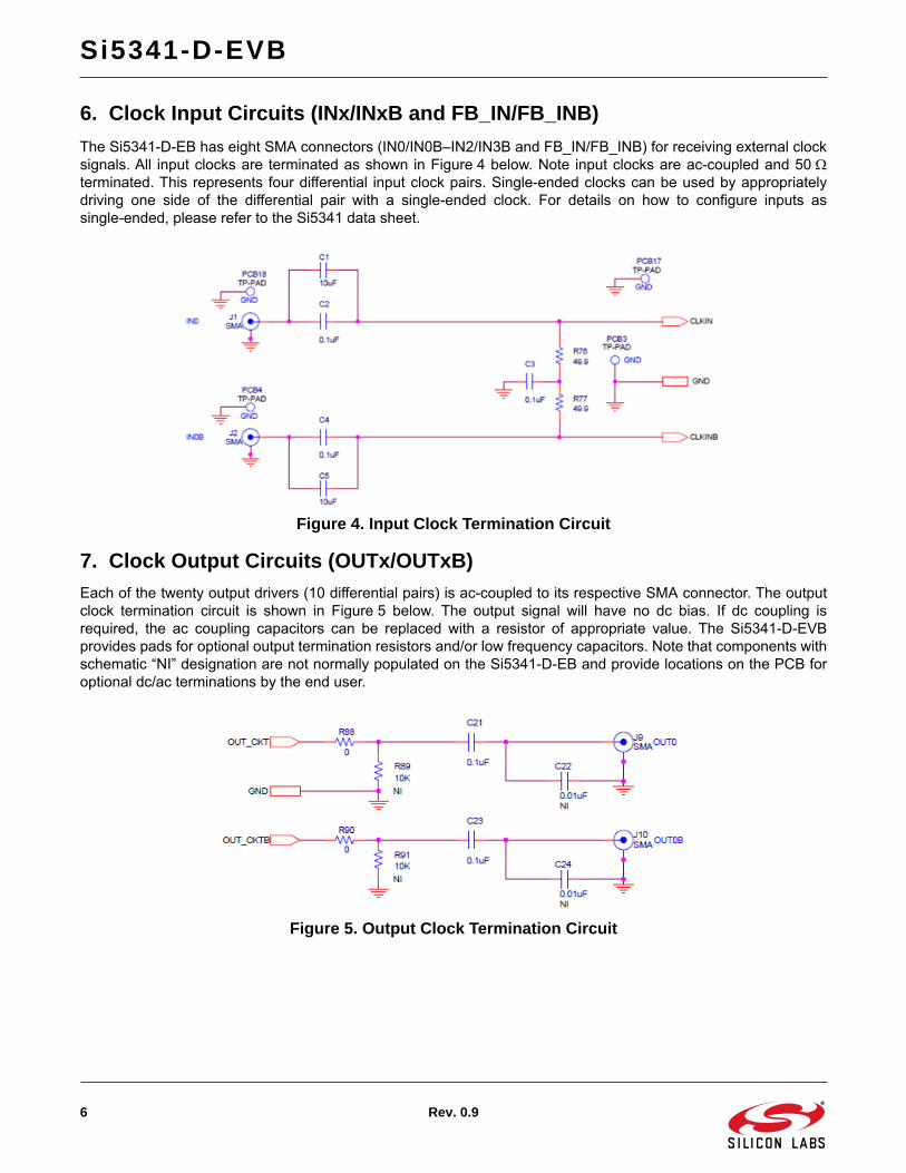
Si5341-D-EVB
6 Rev 09
6 Clock Input Circuits (INxINxB and FB_INFB_INB)The Si5341-D-EB has eight SMA connectors (IN0IN0BndashIN2IN3B and FB_INFB_INB) for receiving external clocksignals All input clocks are terminated as shown in Figure 4 below Note input clocks are ac-coupled and 50 terminated This represents four differential input clock pairs Single-ended clocks can be used by appropriatelydriving one side of the differential pair with a single-ended clock For details on how to configure inputs assingle-ended please refer to the Si5341 data sheet
Figure 4 Input Clock Termination Circuit
7 Clock Output Circuits (OUTxOUTxB)Each of the twenty output drivers (10 differential pairs) is ac-coupled to its respective SMA connector The outputclock termination circuit is shown in Figure 5 below The output signal will have no dc bias If dc coupling isrequired the ac coupling capacitors can be replaced with a resistor of appropriate value The Si5341-D-EVBprovides pads for optional output termination resistors andor low frequency capacitors Note that components withschematic ldquoNIrdquo designation are not normally populated on the Si5341-D-EB and provide locations on the PCB foroptional dcac terminations by the end user
Figure 5 Output Clock Termination Circuit
Si5341-D-EVB
Rev 09 7
8 Installing ClockBuilderPro (CBPro) Desktop SoftwareTo install the CBOPro software on any Windows 7 (or above) PC
Go to httpwwwsilabscomCBPro and download ClockBuilderPro software
Installation instructions and Userrsquos Guide for ClockBuilderPro can be found at the download link shown abovePlease follow the instructions as indicated
9 Using the Si5341-D-EVB91 Connecting the EVB to Your Host PCOnce ClockBuilderPro software is installed connect to the evaluation board with a USB cable as shown below
Figure 6 EVB Connection Diagram
Si5341-D-EVB
8 Rev 09
92 Additional Power SuppliesAlthough additional power (besides the power supplied by the host PCrsquos USB port) is not needed for mostconfigurations two additional +5 VDC power supplies (MAIN and AUX) can be connected to J33 and J34 (locatedon the bottom of the board near the USB connector) Refer to the Si5341-D-EB schematic for details
The Si5341-EB comes preconfigured with jumpers installed at JP15 and JP16 (pins 1-2 in both cases) in order toselect ldquoUSBrdquo These jumpers together with the components installed configure the evaluation board to obtain all+5 V power solely through the main USB connector at J37 This setup is the default configuration and shouldnormally be sufficient
Figure 7 shows the correct installation of the jumper shunts at JP15 and JP16 for default or standard operation
Figure 7 JP15-JP16 Standard Jumper Shunt InstallationErrata NoteSome early versions of the 64-pin Si534x-EBs may have the silkscreen text at JP15-JP16 reversed regarding EXT
and USB ie USB EXT instead of EXT USB Regardless the correct installation of the jumper shunts for defaultor standard operation is on the right hand side as read and viewed in Figure 7
The general guidelines for single USB power supply operation are listed below
Use either a USB 30 or USB 20 port These ports are specified to supply 900 mA and 500 mA respectively at +5 V
If you are working with a USB 20 port and you are current limited turn off enough DUT output voltage regulators to drop the total DUT current le 470 mA (Note USB 20 ports may supply gt 500 mA Provided the nominal +5 V drops gracefully by less than 10 the EVB will still work)
If you are working with a USB 20 and you are current limited and need all output clock drivers enabled re-configure the EB to drive the DUT output voltage regulators from an external +5 V power supply as follows
Connect external +5 V power supply to terminal block J33 on the back side of the PCBMove the jumper at JP15 from pins 1-2 USB to pins 2-3 EXT
Si5341-D-EVB
Rev 09 9
93 Overview of ClockBuilderPro ApplicationsNote The following instructions and screen captures may vary slightly depending on your version of ClockBuilderPro The ClockBuilderPro installer will install two main applications
Figure 8 Application 1 ClockbuilderPro WizardUse the CBPro Wizard to
Create a new design
Review or edit an existing design
Export create in-system programming
Figure 9 Application 2 EVB GUIUse the EVB GUI to
Download configuration to EVBrsquos DUT (Si5341)
Control the EVBrsquos regulators
Monitor voltage current power on the EVB
Si5341-D-EVB
10 Rev 09
94 Common ClockBuilderPro Work Flow ScenariosThere are three common workflow scenarios when using CBPro and the Si5341-D-EVB These workflow scenariosare
Workflow Scenario 1 Testing a Silicon Labs-Created Default Configuration
Workflow Scenario 2 Modifying the Default Silicon Labs-Created Device Configuration
Workflow Scenario 3 Testing a User-Created Device Configuration
Each is described in more detail in the following sections
95 Workflow Scenario 1 Testing a Silicon Labs-Created Default ConfigurationThe flow for using the EVB GUI to initialize and control a device on the EVB is as follows
Once the PC and EVB are connected launch ClockBuilder Pro by clicking on this icon on your PCrsquos desktop
Figure 10 ClockBuilderPro Desktop IconIf an EVB is detected click on the ldquoOpen Default Planrdquo button on the Wizardrsquos main menu CBPro automaticallydetects the EVB and device type
Figure 11 Open Default PlanOnce you open the default plan (based on your EVB model number) a popup will appear
Figure 12 Write Design to EVB DialogSelect ldquoYesrdquo to write the default plan to the Si5341 device mounted on your EVB This ensures the device iscompletely reconfigured per the Silicon Labs default plan for the DUT type mounted on the EVB
Si5341-D-EVB
Rev 09 11
Figure 13 Writing Design StatusAfter CBPro writes the default plan to the EVB click on ldquoOpen EVB GUIrdquo as shown below
Figure 14 Open EVB GUIThe EVB GUI will appear Note all power supplies will be set to the values defined in the devicersquos default CBProproject file created by Silicon Labs as shown below
Figure 15 EVB GUI Window
Si5341-D-EVB
12 Rev 09
951 Verify Free-Run Mode OperationAssuming no external clocks have been connected to the INPUT CLOCK differential SMA connectors (labeledldquoINxINxBrdquo) located around the perimeter of the EVB the DUT should now be operating in free-run mode as theDUT will be locked to the crystal in this case
You can run a quick check to determine if the device is powered up and generating output clocks (and consumingpower) by clicking on the Read All button highlighted above and then reviewing the voltage current and powerreadings for each VDDx supply
Note Shutting ldquoOffrdquo then ldquoOnrdquo of the VDD and VDDA supplies will power-down and reset the DUT Every time you dothis to reload the Silicon Labs-created default plan into the DUTrsquos register space you must go back to the Wiz-ardrsquos main menu and select ldquoWrite Design to EVBrdquo
Figure 16 Write Design to EVBFailure to do the step above will cause the device to read in a pre-programmed plan from its non-volatilememory (NVM) However the plan loaded from the NVM may not be the latest plan recommended bySilicon Labs for evaluationAt this point you should verify the presence and frequencies of the output clocks (running to free-run mode fromthe crystal) using appropriate external instrumentation connected to the output clock SMA connectors To verify theoutput clocks are toggling at the correct frequency and signal format click on View Design Report as highlightedbelow
Figure 17 View Design Report
Si5341-D-EVB
Rev 09 13
Your configurationrsquos design report will appear in a new window as shown below Compare the observed outputclocks to the frequencies and formats noted in your default projectrsquos Design Report
Figure 18 Design Report Window952 Verify Locked Mode OperationAssuming you connect the correct input clocks to the EVB (as noted in the Design Report shown above) the DUTon your EVB will be running in ldquolockedrdquo mode
Si5341-D-EVB
14 Rev 09
96 Workflow Scenario 2 Modifying the Default Silicon Labs-Created DeviceConfiguration
To modify the ldquodefaultrdquo configuration using the CBPro Wizard click on Edit Configuration with Wizard
Figure 19 Edit Configuration with WizardYou will now be taken to the Wizardrsquos step-by-step menus to allow you to change any of the default planrsquosoperating configurations
Figure 20 Design Wizard
Si5341-D-EVB
Rev 09 15
Note you can click on the icon on the lower left hand corner of the menu to confirm if your frequency plan is validAfter making your desired changes you can click on Write to EVB to update the DUT to reconfigure your devicereal-time The Design Write status window will appear each time you make a change
Figure 21 Writing Design Status
97 Workflow Scenario 3 Testing a User-Created Device ConfigurationTo test a previously created user configuration open the CBPro Wizard by clicking on the icon on your desktop andthen selecting Open Design Project File
Figure 22 Open Design Project File
Si5341-D-EVB
16 Rev 09
Locate your CBPro design file (slabtimeproj or sitproj file)design file in the Windows file browser
Figure 23 Browse to Project FileSelect Yes when the WRITE DESIGN to EVB popup appears
Figure 24 Write Design to EVB DialogThe progress bar will be launched Once the new design project file has been written to the device verify thepresence and frequencies of your output clocks and other operating configurations using external instrumentation
Si5341-D-EVB
Rev 09 17
98 Exporting the Register Map File for Device Programming by a Host ProcessorYou can also export your configuration to a file format suitable for in-system programming by selecting Export asshown below
Figure 25 Export Register Map FileYou can now write your devicersquos complete configuration to file formats suitable for in-system programming
Figure 26 Export Settings
Si5341-D-EVB
18 Rev 09
10 Writing a New Frequency Plan or Device Configuration to Non-Volatile Memory (OTP)
Note Writing to the device non-volatile memory (OTP) is NOT the same as writing a configuration into the Si5341 using Clock-BuilderPro on the Si5341-D-EB Writing a configuration into the EVB from ClockBuilderPro is done using Si5341 RAMspace and can be done virtually unlimited numbers of times Writing to OTP is limited as described below
Refer to the Si534x8x Family Reference Manuals and device data sheets for information on how to write aconfiguration to the EVB DUTrsquos non-volatile memory (OTP) The OTP can be programmed a maximum of twotimes only Care must be taken to ensure the configuration desired is valid when choosing to write to OTP
11 Si5341-D-EVB Schematic and Bill of Materials (BOM)The Si5341-D-EVB Schematic and Bill of Materials (BOM) can be found online at
httpwwwsilabscomproductsclocksoscillatorspagessi538x-4x-evbaspx
Note Please be aware that the Si5341-D-EB schematic is in OrCad Capture hierarchical format and not in a typical ldquoflatrdquoschematic format
httpwwwsilabscom
Silicon Laboratories Inc400 West Cesar ChavezAustin TX 78701USA
ClockBuilder ProOne-click access to Timing tools documentation software source code libraries amp more Available for Windows and iOS (CBGo only)
wwwsilabscomCBPro
Timing Portfoliowwwsilabscomtiming
SWHWwwwsilabscomCBPro
Qualitywwwsilabscomquality
Support and Communitycommunitysilabscom
DisclaimerSilicon Laboratories intends to provide customers with the latest accurate and in-depth documentation of all peripherals and modules available for system and software implementers using or intending to use the Silicon Laboratories products Characterization data available modules and peripherals memory sizes and memory addresses refer to each specific device and Typical parameters provided can and do vary in different applications Application examples described herein are for illustrative purposes only Silicon Laboratories reserves the right to make changes without further notice and limitation to product information specifications and descriptions herein and does not give warranties as to the accuracy or completeness of the included information Silicon Laboratories shall have no liability for the consequences of use of the information supplied herein This document does not imply or express copyright licenses granted hereunder to design or fabricate any integrated circuits The products are not designed or authorized to be used within any Life Support System without the specific written consent of Silicon Laboratories A Life Support System is any product or system intended to support or sustain life andor health which if it fails can be reasonably expected to result in significant personal injury or death Silicon Laboratories products are not designed or authorized for military applications Silicon Laboratories products shall under no circumstances be used in weapons of mass destruction including (but not limited to) nuclear biological or chemical weapons or missiles capable of delivering such weapons
Trademark InformationSilicon Laboratories Increg Silicon Laboratoriesreg Silicon Labsreg SiLabsreg and the Silicon Labs logoreg Bluegigareg Bluegiga Logoreg Clockbuilderreg CMEMSreg DSPLLreg EFMreg EFM32reg EFR Emberreg Energy Micro Energy Micro logo and combinations thereof the worldrsquos most energy friendly microcontrollers Emberreg EZLinkreg EZRadioreg EZRadioPROreg Geckoreg ISOmodemreg Precision32reg ProSLICreg Simplicity Studioreg SiPHYreg Telegesis the Telegesis Logoreg USBXpressreg and others are trademarks or registered trademarks of Silicon Laborato-ries Inc ARM CORTEX Cortex-M3 and THUMB are trademarks or registered trademarks of ARM Holdings Keil is a registered trademark of ARM Limited All other products or brand names mentioned herein are trademarks of their respective holders
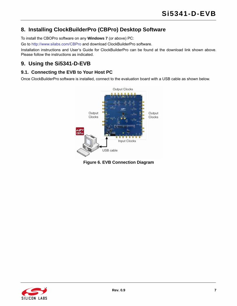
Si5341-D-EVB
Rev 09 7
8 Installing ClockBuilderPro (CBPro) Desktop SoftwareTo install the CBOPro software on any Windows 7 (or above) PC
Go to httpwwwsilabscomCBPro and download ClockBuilderPro software
Installation instructions and Userrsquos Guide for ClockBuilderPro can be found at the download link shown abovePlease follow the instructions as indicated
9 Using the Si5341-D-EVB91 Connecting the EVB to Your Host PCOnce ClockBuilderPro software is installed connect to the evaluation board with a USB cable as shown below
Figure 6 EVB Connection Diagram
Si5341-D-EVB
8 Rev 09
92 Additional Power SuppliesAlthough additional power (besides the power supplied by the host PCrsquos USB port) is not needed for mostconfigurations two additional +5 VDC power supplies (MAIN and AUX) can be connected to J33 and J34 (locatedon the bottom of the board near the USB connector) Refer to the Si5341-D-EB schematic for details
The Si5341-EB comes preconfigured with jumpers installed at JP15 and JP16 (pins 1-2 in both cases) in order toselect ldquoUSBrdquo These jumpers together with the components installed configure the evaluation board to obtain all+5 V power solely through the main USB connector at J37 This setup is the default configuration and shouldnormally be sufficient
Figure 7 shows the correct installation of the jumper shunts at JP15 and JP16 for default or standard operation
Figure 7 JP15-JP16 Standard Jumper Shunt InstallationErrata NoteSome early versions of the 64-pin Si534x-EBs may have the silkscreen text at JP15-JP16 reversed regarding EXT
and USB ie USB EXT instead of EXT USB Regardless the correct installation of the jumper shunts for defaultor standard operation is on the right hand side as read and viewed in Figure 7
The general guidelines for single USB power supply operation are listed below
Use either a USB 30 or USB 20 port These ports are specified to supply 900 mA and 500 mA respectively at +5 V
If you are working with a USB 20 port and you are current limited turn off enough DUT output voltage regulators to drop the total DUT current le 470 mA (Note USB 20 ports may supply gt 500 mA Provided the nominal +5 V drops gracefully by less than 10 the EVB will still work)
If you are working with a USB 20 and you are current limited and need all output clock drivers enabled re-configure the EB to drive the DUT output voltage regulators from an external +5 V power supply as follows
Connect external +5 V power supply to terminal block J33 on the back side of the PCBMove the jumper at JP15 from pins 1-2 USB to pins 2-3 EXT
Si5341-D-EVB
Rev 09 9
93 Overview of ClockBuilderPro ApplicationsNote The following instructions and screen captures may vary slightly depending on your version of ClockBuilderPro The ClockBuilderPro installer will install two main applications
Figure 8 Application 1 ClockbuilderPro WizardUse the CBPro Wizard to
Create a new design
Review or edit an existing design
Export create in-system programming
Figure 9 Application 2 EVB GUIUse the EVB GUI to
Download configuration to EVBrsquos DUT (Si5341)
Control the EVBrsquos regulators
Monitor voltage current power on the EVB
Si5341-D-EVB
10 Rev 09
94 Common ClockBuilderPro Work Flow ScenariosThere are three common workflow scenarios when using CBPro and the Si5341-D-EVB These workflow scenariosare
Workflow Scenario 1 Testing a Silicon Labs-Created Default Configuration
Workflow Scenario 2 Modifying the Default Silicon Labs-Created Device Configuration
Workflow Scenario 3 Testing a User-Created Device Configuration
Each is described in more detail in the following sections
95 Workflow Scenario 1 Testing a Silicon Labs-Created Default ConfigurationThe flow for using the EVB GUI to initialize and control a device on the EVB is as follows
Once the PC and EVB are connected launch ClockBuilder Pro by clicking on this icon on your PCrsquos desktop
Figure 10 ClockBuilderPro Desktop IconIf an EVB is detected click on the ldquoOpen Default Planrdquo button on the Wizardrsquos main menu CBPro automaticallydetects the EVB and device type
Figure 11 Open Default PlanOnce you open the default plan (based on your EVB model number) a popup will appear
Figure 12 Write Design to EVB DialogSelect ldquoYesrdquo to write the default plan to the Si5341 device mounted on your EVB This ensures the device iscompletely reconfigured per the Silicon Labs default plan for the DUT type mounted on the EVB
Si5341-D-EVB
Rev 09 11
Figure 13 Writing Design StatusAfter CBPro writes the default plan to the EVB click on ldquoOpen EVB GUIrdquo as shown below
Figure 14 Open EVB GUIThe EVB GUI will appear Note all power supplies will be set to the values defined in the devicersquos default CBProproject file created by Silicon Labs as shown below
Figure 15 EVB GUI Window
Si5341-D-EVB
12 Rev 09
951 Verify Free-Run Mode OperationAssuming no external clocks have been connected to the INPUT CLOCK differential SMA connectors (labeledldquoINxINxBrdquo) located around the perimeter of the EVB the DUT should now be operating in free-run mode as theDUT will be locked to the crystal in this case
You can run a quick check to determine if the device is powered up and generating output clocks (and consumingpower) by clicking on the Read All button highlighted above and then reviewing the voltage current and powerreadings for each VDDx supply
Note Shutting ldquoOffrdquo then ldquoOnrdquo of the VDD and VDDA supplies will power-down and reset the DUT Every time you dothis to reload the Silicon Labs-created default plan into the DUTrsquos register space you must go back to the Wiz-ardrsquos main menu and select ldquoWrite Design to EVBrdquo
Figure 16 Write Design to EVBFailure to do the step above will cause the device to read in a pre-programmed plan from its non-volatilememory (NVM) However the plan loaded from the NVM may not be the latest plan recommended bySilicon Labs for evaluationAt this point you should verify the presence and frequencies of the output clocks (running to free-run mode fromthe crystal) using appropriate external instrumentation connected to the output clock SMA connectors To verify theoutput clocks are toggling at the correct frequency and signal format click on View Design Report as highlightedbelow
Figure 17 View Design Report
Si5341-D-EVB
Rev 09 13
Your configurationrsquos design report will appear in a new window as shown below Compare the observed outputclocks to the frequencies and formats noted in your default projectrsquos Design Report
Figure 18 Design Report Window952 Verify Locked Mode OperationAssuming you connect the correct input clocks to the EVB (as noted in the Design Report shown above) the DUTon your EVB will be running in ldquolockedrdquo mode
Si5341-D-EVB
14 Rev 09
96 Workflow Scenario 2 Modifying the Default Silicon Labs-Created DeviceConfiguration
To modify the ldquodefaultrdquo configuration using the CBPro Wizard click on Edit Configuration with Wizard
Figure 19 Edit Configuration with WizardYou will now be taken to the Wizardrsquos step-by-step menus to allow you to change any of the default planrsquosoperating configurations
Figure 20 Design Wizard
Si5341-D-EVB
Rev 09 15
Note you can click on the icon on the lower left hand corner of the menu to confirm if your frequency plan is validAfter making your desired changes you can click on Write to EVB to update the DUT to reconfigure your devicereal-time The Design Write status window will appear each time you make a change
Figure 21 Writing Design Status
97 Workflow Scenario 3 Testing a User-Created Device ConfigurationTo test a previously created user configuration open the CBPro Wizard by clicking on the icon on your desktop andthen selecting Open Design Project File
Figure 22 Open Design Project File
Si5341-D-EVB
16 Rev 09
Locate your CBPro design file (slabtimeproj or sitproj file)design file in the Windows file browser
Figure 23 Browse to Project FileSelect Yes when the WRITE DESIGN to EVB popup appears
Figure 24 Write Design to EVB DialogThe progress bar will be launched Once the new design project file has been written to the device verify thepresence and frequencies of your output clocks and other operating configurations using external instrumentation
Si5341-D-EVB
Rev 09 17
98 Exporting the Register Map File for Device Programming by a Host ProcessorYou can also export your configuration to a file format suitable for in-system programming by selecting Export asshown below
Figure 25 Export Register Map FileYou can now write your devicersquos complete configuration to file formats suitable for in-system programming
Figure 26 Export Settings
Si5341-D-EVB
18 Rev 09
10 Writing a New Frequency Plan or Device Configuration to Non-Volatile Memory (OTP)
Note Writing to the device non-volatile memory (OTP) is NOT the same as writing a configuration into the Si5341 using Clock-BuilderPro on the Si5341-D-EB Writing a configuration into the EVB from ClockBuilderPro is done using Si5341 RAMspace and can be done virtually unlimited numbers of times Writing to OTP is limited as described below
Refer to the Si534x8x Family Reference Manuals and device data sheets for information on how to write aconfiguration to the EVB DUTrsquos non-volatile memory (OTP) The OTP can be programmed a maximum of twotimes only Care must be taken to ensure the configuration desired is valid when choosing to write to OTP
11 Si5341-D-EVB Schematic and Bill of Materials (BOM)The Si5341-D-EVB Schematic and Bill of Materials (BOM) can be found online at
httpwwwsilabscomproductsclocksoscillatorspagessi538x-4x-evbaspx
Note Please be aware that the Si5341-D-EB schematic is in OrCad Capture hierarchical format and not in a typical ldquoflatrdquoschematic format
httpwwwsilabscom
Silicon Laboratories Inc400 West Cesar ChavezAustin TX 78701USA
ClockBuilder ProOne-click access to Timing tools documentation software source code libraries amp more Available for Windows and iOS (CBGo only)
wwwsilabscomCBPro
Timing Portfoliowwwsilabscomtiming
SWHWwwwsilabscomCBPro
Qualitywwwsilabscomquality
Support and Communitycommunitysilabscom
DisclaimerSilicon Laboratories intends to provide customers with the latest accurate and in-depth documentation of all peripherals and modules available for system and software implementers using or intending to use the Silicon Laboratories products Characterization data available modules and peripherals memory sizes and memory addresses refer to each specific device and Typical parameters provided can and do vary in different applications Application examples described herein are for illustrative purposes only Silicon Laboratories reserves the right to make changes without further notice and limitation to product information specifications and descriptions herein and does not give warranties as to the accuracy or completeness of the included information Silicon Laboratories shall have no liability for the consequences of use of the information supplied herein This document does not imply or express copyright licenses granted hereunder to design or fabricate any integrated circuits The products are not designed or authorized to be used within any Life Support System without the specific written consent of Silicon Laboratories A Life Support System is any product or system intended to support or sustain life andor health which if it fails can be reasonably expected to result in significant personal injury or death Silicon Laboratories products are not designed or authorized for military applications Silicon Laboratories products shall under no circumstances be used in weapons of mass destruction including (but not limited to) nuclear biological or chemical weapons or missiles capable of delivering such weapons
Trademark InformationSilicon Laboratories Increg Silicon Laboratoriesreg Silicon Labsreg SiLabsreg and the Silicon Labs logoreg Bluegigareg Bluegiga Logoreg Clockbuilderreg CMEMSreg DSPLLreg EFMreg EFM32reg EFR Emberreg Energy Micro Energy Micro logo and combinations thereof the worldrsquos most energy friendly microcontrollers Emberreg EZLinkreg EZRadioreg EZRadioPROreg Geckoreg ISOmodemreg Precision32reg ProSLICreg Simplicity Studioreg SiPHYreg Telegesis the Telegesis Logoreg USBXpressreg and others are trademarks or registered trademarks of Silicon Laborato-ries Inc ARM CORTEX Cortex-M3 and THUMB are trademarks or registered trademarks of ARM Holdings Keil is a registered trademark of ARM Limited All other products or brand names mentioned herein are trademarks of their respective holders
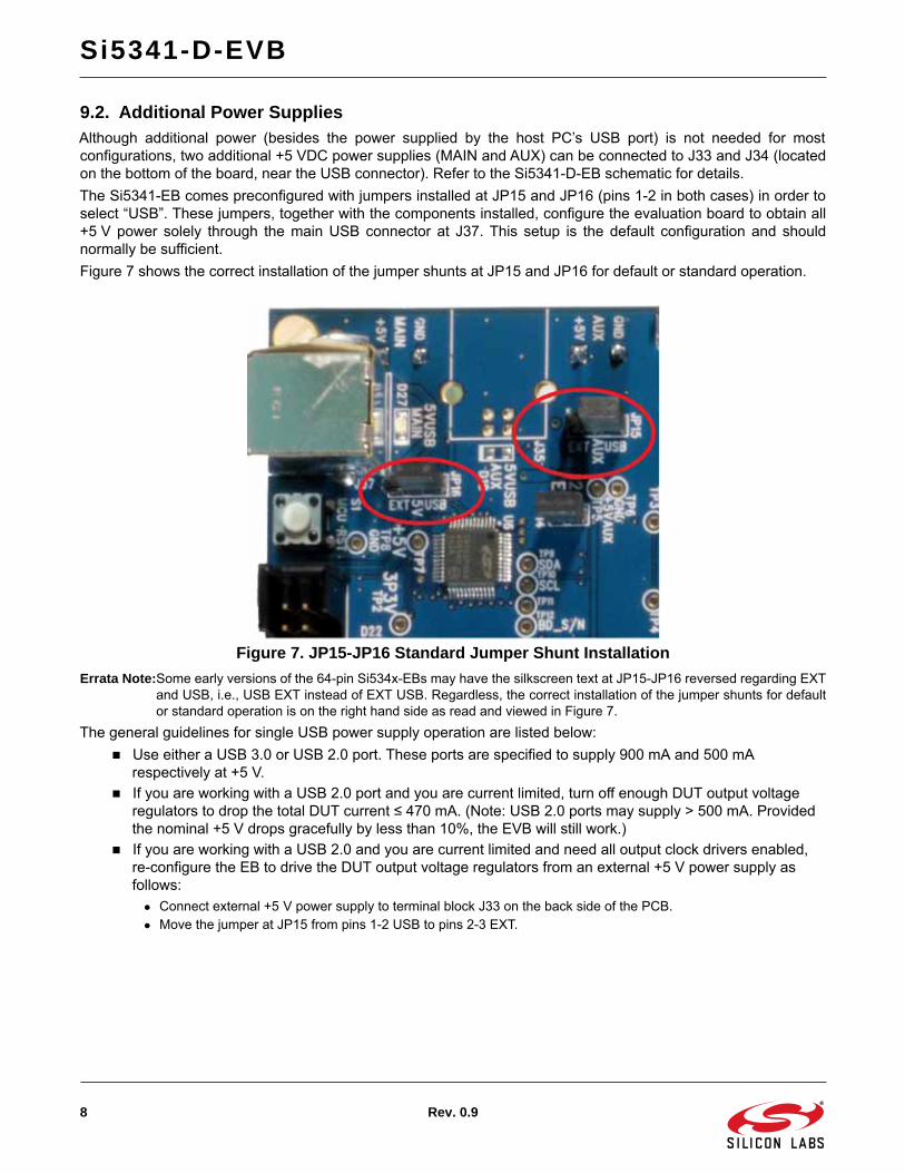
Si5341-D-EVB
8 Rev 09
92 Additional Power SuppliesAlthough additional power (besides the power supplied by the host PCrsquos USB port) is not needed for mostconfigurations two additional +5 VDC power supplies (MAIN and AUX) can be connected to J33 and J34 (locatedon the bottom of the board near the USB connector) Refer to the Si5341-D-EB schematic for details
The Si5341-EB comes preconfigured with jumpers installed at JP15 and JP16 (pins 1-2 in both cases) in order toselect ldquoUSBrdquo These jumpers together with the components installed configure the evaluation board to obtain all+5 V power solely through the main USB connector at J37 This setup is the default configuration and shouldnormally be sufficient
Figure 7 shows the correct installation of the jumper shunts at JP15 and JP16 for default or standard operation
Figure 7 JP15-JP16 Standard Jumper Shunt InstallationErrata NoteSome early versions of the 64-pin Si534x-EBs may have the silkscreen text at JP15-JP16 reversed regarding EXT
and USB ie USB EXT instead of EXT USB Regardless the correct installation of the jumper shunts for defaultor standard operation is on the right hand side as read and viewed in Figure 7
The general guidelines for single USB power supply operation are listed below
Use either a USB 30 or USB 20 port These ports are specified to supply 900 mA and 500 mA respectively at +5 V
If you are working with a USB 20 port and you are current limited turn off enough DUT output voltage regulators to drop the total DUT current le 470 mA (Note USB 20 ports may supply gt 500 mA Provided the nominal +5 V drops gracefully by less than 10 the EVB will still work)
If you are working with a USB 20 and you are current limited and need all output clock drivers enabled re-configure the EB to drive the DUT output voltage regulators from an external +5 V power supply as follows
Connect external +5 V power supply to terminal block J33 on the back side of the PCBMove the jumper at JP15 from pins 1-2 USB to pins 2-3 EXT
Si5341-D-EVB
Rev 09 9
93 Overview of ClockBuilderPro ApplicationsNote The following instructions and screen captures may vary slightly depending on your version of ClockBuilderPro The ClockBuilderPro installer will install two main applications
Figure 8 Application 1 ClockbuilderPro WizardUse the CBPro Wizard to
Create a new design
Review or edit an existing design
Export create in-system programming
Figure 9 Application 2 EVB GUIUse the EVB GUI to
Download configuration to EVBrsquos DUT (Si5341)
Control the EVBrsquos regulators
Monitor voltage current power on the EVB
Si5341-D-EVB
10 Rev 09
94 Common ClockBuilderPro Work Flow ScenariosThere are three common workflow scenarios when using CBPro and the Si5341-D-EVB These workflow scenariosare
Workflow Scenario 1 Testing a Silicon Labs-Created Default Configuration
Workflow Scenario 2 Modifying the Default Silicon Labs-Created Device Configuration
Workflow Scenario 3 Testing a User-Created Device Configuration
Each is described in more detail in the following sections
95 Workflow Scenario 1 Testing a Silicon Labs-Created Default ConfigurationThe flow for using the EVB GUI to initialize and control a device on the EVB is as follows
Once the PC and EVB are connected launch ClockBuilder Pro by clicking on this icon on your PCrsquos desktop
Figure 10 ClockBuilderPro Desktop IconIf an EVB is detected click on the ldquoOpen Default Planrdquo button on the Wizardrsquos main menu CBPro automaticallydetects the EVB and device type
Figure 11 Open Default PlanOnce you open the default plan (based on your EVB model number) a popup will appear
Figure 12 Write Design to EVB DialogSelect ldquoYesrdquo to write the default plan to the Si5341 device mounted on your EVB This ensures the device iscompletely reconfigured per the Silicon Labs default plan for the DUT type mounted on the EVB
Si5341-D-EVB
Rev 09 11
Figure 13 Writing Design StatusAfter CBPro writes the default plan to the EVB click on ldquoOpen EVB GUIrdquo as shown below
Figure 14 Open EVB GUIThe EVB GUI will appear Note all power supplies will be set to the values defined in the devicersquos default CBProproject file created by Silicon Labs as shown below
Figure 15 EVB GUI Window
Si5341-D-EVB
12 Rev 09
951 Verify Free-Run Mode OperationAssuming no external clocks have been connected to the INPUT CLOCK differential SMA connectors (labeledldquoINxINxBrdquo) located around the perimeter of the EVB the DUT should now be operating in free-run mode as theDUT will be locked to the crystal in this case
You can run a quick check to determine if the device is powered up and generating output clocks (and consumingpower) by clicking on the Read All button highlighted above and then reviewing the voltage current and powerreadings for each VDDx supply
Note Shutting ldquoOffrdquo then ldquoOnrdquo of the VDD and VDDA supplies will power-down and reset the DUT Every time you dothis to reload the Silicon Labs-created default plan into the DUTrsquos register space you must go back to the Wiz-ardrsquos main menu and select ldquoWrite Design to EVBrdquo
Figure 16 Write Design to EVBFailure to do the step above will cause the device to read in a pre-programmed plan from its non-volatilememory (NVM) However the plan loaded from the NVM may not be the latest plan recommended bySilicon Labs for evaluationAt this point you should verify the presence and frequencies of the output clocks (running to free-run mode fromthe crystal) using appropriate external instrumentation connected to the output clock SMA connectors To verify theoutput clocks are toggling at the correct frequency and signal format click on View Design Report as highlightedbelow
Figure 17 View Design Report
Si5341-D-EVB
Rev 09 13
Your configurationrsquos design report will appear in a new window as shown below Compare the observed outputclocks to the frequencies and formats noted in your default projectrsquos Design Report
Figure 18 Design Report Window952 Verify Locked Mode OperationAssuming you connect the correct input clocks to the EVB (as noted in the Design Report shown above) the DUTon your EVB will be running in ldquolockedrdquo mode
Si5341-D-EVB
14 Rev 09
96 Workflow Scenario 2 Modifying the Default Silicon Labs-Created DeviceConfiguration
To modify the ldquodefaultrdquo configuration using the CBPro Wizard click on Edit Configuration with Wizard
Figure 19 Edit Configuration with WizardYou will now be taken to the Wizardrsquos step-by-step menus to allow you to change any of the default planrsquosoperating configurations
Figure 20 Design Wizard
Si5341-D-EVB
Rev 09 15
Note you can click on the icon on the lower left hand corner of the menu to confirm if your frequency plan is validAfter making your desired changes you can click on Write to EVB to update the DUT to reconfigure your devicereal-time The Design Write status window will appear each time you make a change
Figure 21 Writing Design Status
97 Workflow Scenario 3 Testing a User-Created Device ConfigurationTo test a previously created user configuration open the CBPro Wizard by clicking on the icon on your desktop andthen selecting Open Design Project File
Figure 22 Open Design Project File
Si5341-D-EVB
16 Rev 09
Locate your CBPro design file (slabtimeproj or sitproj file)design file in the Windows file browser
Figure 23 Browse to Project FileSelect Yes when the WRITE DESIGN to EVB popup appears
Figure 24 Write Design to EVB DialogThe progress bar will be launched Once the new design project file has been written to the device verify thepresence and frequencies of your output clocks and other operating configurations using external instrumentation
Si5341-D-EVB
Rev 09 17
98 Exporting the Register Map File for Device Programming by a Host ProcessorYou can also export your configuration to a file format suitable for in-system programming by selecting Export asshown below
Figure 25 Export Register Map FileYou can now write your devicersquos complete configuration to file formats suitable for in-system programming
Figure 26 Export Settings
Si5341-D-EVB
18 Rev 09
10 Writing a New Frequency Plan or Device Configuration to Non-Volatile Memory (OTP)
Note Writing to the device non-volatile memory (OTP) is NOT the same as writing a configuration into the Si5341 using Clock-BuilderPro on the Si5341-D-EB Writing a configuration into the EVB from ClockBuilderPro is done using Si5341 RAMspace and can be done virtually unlimited numbers of times Writing to OTP is limited as described below
Refer to the Si534x8x Family Reference Manuals and device data sheets for information on how to write aconfiguration to the EVB DUTrsquos non-volatile memory (OTP) The OTP can be programmed a maximum of twotimes only Care must be taken to ensure the configuration desired is valid when choosing to write to OTP
11 Si5341-D-EVB Schematic and Bill of Materials (BOM)The Si5341-D-EVB Schematic and Bill of Materials (BOM) can be found online at
httpwwwsilabscomproductsclocksoscillatorspagessi538x-4x-evbaspx
Note Please be aware that the Si5341-D-EB schematic is in OrCad Capture hierarchical format and not in a typical ldquoflatrdquoschematic format
httpwwwsilabscom
Silicon Laboratories Inc400 West Cesar ChavezAustin TX 78701USA
ClockBuilder ProOne-click access to Timing tools documentation software source code libraries amp more Available for Windows and iOS (CBGo only)
wwwsilabscomCBPro
Timing Portfoliowwwsilabscomtiming
SWHWwwwsilabscomCBPro
Qualitywwwsilabscomquality
Support and Communitycommunitysilabscom
DisclaimerSilicon Laboratories intends to provide customers with the latest accurate and in-depth documentation of all peripherals and modules available for system and software implementers using or intending to use the Silicon Laboratories products Characterization data available modules and peripherals memory sizes and memory addresses refer to each specific device and Typical parameters provided can and do vary in different applications Application examples described herein are for illustrative purposes only Silicon Laboratories reserves the right to make changes without further notice and limitation to product information specifications and descriptions herein and does not give warranties as to the accuracy or completeness of the included information Silicon Laboratories shall have no liability for the consequences of use of the information supplied herein This document does not imply or express copyright licenses granted hereunder to design or fabricate any integrated circuits The products are not designed or authorized to be used within any Life Support System without the specific written consent of Silicon Laboratories A Life Support System is any product or system intended to support or sustain life andor health which if it fails can be reasonably expected to result in significant personal injury or death Silicon Laboratories products are not designed or authorized for military applications Silicon Laboratories products shall under no circumstances be used in weapons of mass destruction including (but not limited to) nuclear biological or chemical weapons or missiles capable of delivering such weapons
Trademark InformationSilicon Laboratories Increg Silicon Laboratoriesreg Silicon Labsreg SiLabsreg and the Silicon Labs logoreg Bluegigareg Bluegiga Logoreg Clockbuilderreg CMEMSreg DSPLLreg EFMreg EFM32reg EFR Emberreg Energy Micro Energy Micro logo and combinations thereof the worldrsquos most energy friendly microcontrollers Emberreg EZLinkreg EZRadioreg EZRadioPROreg Geckoreg ISOmodemreg Precision32reg ProSLICreg Simplicity Studioreg SiPHYreg Telegesis the Telegesis Logoreg USBXpressreg and others are trademarks or registered trademarks of Silicon Laborato-ries Inc ARM CORTEX Cortex-M3 and THUMB are trademarks or registered trademarks of ARM Holdings Keil is a registered trademark of ARM Limited All other products or brand names mentioned herein are trademarks of their respective holders
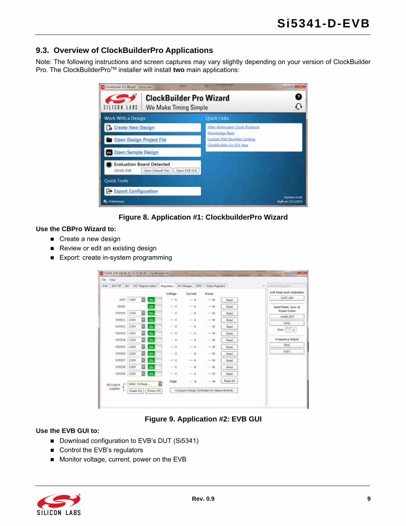
Si5341-D-EVB
Rev 09 9
93 Overview of ClockBuilderPro ApplicationsNote The following instructions and screen captures may vary slightly depending on your version of ClockBuilderPro The ClockBuilderPro installer will install two main applications
Figure 8 Application 1 ClockbuilderPro WizardUse the CBPro Wizard to
Create a new design
Review or edit an existing design
Export create in-system programming
Figure 9 Application 2 EVB GUIUse the EVB GUI to
Download configuration to EVBrsquos DUT (Si5341)
Control the EVBrsquos regulators
Monitor voltage current power on the EVB
Si5341-D-EVB
10 Rev 09
94 Common ClockBuilderPro Work Flow ScenariosThere are three common workflow scenarios when using CBPro and the Si5341-D-EVB These workflow scenariosare
Workflow Scenario 1 Testing a Silicon Labs-Created Default Configuration
Workflow Scenario 2 Modifying the Default Silicon Labs-Created Device Configuration
Workflow Scenario 3 Testing a User-Created Device Configuration
Each is described in more detail in the following sections
95 Workflow Scenario 1 Testing a Silicon Labs-Created Default ConfigurationThe flow for using the EVB GUI to initialize and control a device on the EVB is as follows
Once the PC and EVB are connected launch ClockBuilder Pro by clicking on this icon on your PCrsquos desktop
Figure 10 ClockBuilderPro Desktop IconIf an EVB is detected click on the ldquoOpen Default Planrdquo button on the Wizardrsquos main menu CBPro automaticallydetects the EVB and device type
Figure 11 Open Default PlanOnce you open the default plan (based on your EVB model number) a popup will appear
Figure 12 Write Design to EVB DialogSelect ldquoYesrdquo to write the default plan to the Si5341 device mounted on your EVB This ensures the device iscompletely reconfigured per the Silicon Labs default plan for the DUT type mounted on the EVB
Si5341-D-EVB
Rev 09 11
Figure 13 Writing Design StatusAfter CBPro writes the default plan to the EVB click on ldquoOpen EVB GUIrdquo as shown below
Figure 14 Open EVB GUIThe EVB GUI will appear Note all power supplies will be set to the values defined in the devicersquos default CBProproject file created by Silicon Labs as shown below
Figure 15 EVB GUI Window
Si5341-D-EVB
12 Rev 09
951 Verify Free-Run Mode OperationAssuming no external clocks have been connected to the INPUT CLOCK differential SMA connectors (labeledldquoINxINxBrdquo) located around the perimeter of the EVB the DUT should now be operating in free-run mode as theDUT will be locked to the crystal in this case
You can run a quick check to determine if the device is powered up and generating output clocks (and consumingpower) by clicking on the Read All button highlighted above and then reviewing the voltage current and powerreadings for each VDDx supply
Note Shutting ldquoOffrdquo then ldquoOnrdquo of the VDD and VDDA supplies will power-down and reset the DUT Every time you dothis to reload the Silicon Labs-created default plan into the DUTrsquos register space you must go back to the Wiz-ardrsquos main menu and select ldquoWrite Design to EVBrdquo
Figure 16 Write Design to EVBFailure to do the step above will cause the device to read in a pre-programmed plan from its non-volatilememory (NVM) However the plan loaded from the NVM may not be the latest plan recommended bySilicon Labs for evaluationAt this point you should verify the presence and frequencies of the output clocks (running to free-run mode fromthe crystal) using appropriate external instrumentation connected to the output clock SMA connectors To verify theoutput clocks are toggling at the correct frequency and signal format click on View Design Report as highlightedbelow
Figure 17 View Design Report
Si5341-D-EVB
Rev 09 13
Your configurationrsquos design report will appear in a new window as shown below Compare the observed outputclocks to the frequencies and formats noted in your default projectrsquos Design Report
Figure 18 Design Report Window952 Verify Locked Mode OperationAssuming you connect the correct input clocks to the EVB (as noted in the Design Report shown above) the DUTon your EVB will be running in ldquolockedrdquo mode
Si5341-D-EVB
14 Rev 09
96 Workflow Scenario 2 Modifying the Default Silicon Labs-Created DeviceConfiguration
To modify the ldquodefaultrdquo configuration using the CBPro Wizard click on Edit Configuration with Wizard
Figure 19 Edit Configuration with WizardYou will now be taken to the Wizardrsquos step-by-step menus to allow you to change any of the default planrsquosoperating configurations
Figure 20 Design Wizard
Si5341-D-EVB
Rev 09 15
Note you can click on the icon on the lower left hand corner of the menu to confirm if your frequency plan is validAfter making your desired changes you can click on Write to EVB to update the DUT to reconfigure your devicereal-time The Design Write status window will appear each time you make a change
Figure 21 Writing Design Status
97 Workflow Scenario 3 Testing a User-Created Device ConfigurationTo test a previously created user configuration open the CBPro Wizard by clicking on the icon on your desktop andthen selecting Open Design Project File
Figure 22 Open Design Project File
Si5341-D-EVB
16 Rev 09
Locate your CBPro design file (slabtimeproj or sitproj file)design file in the Windows file browser
Figure 23 Browse to Project FileSelect Yes when the WRITE DESIGN to EVB popup appears
Figure 24 Write Design to EVB DialogThe progress bar will be launched Once the new design project file has been written to the device verify thepresence and frequencies of your output clocks and other operating configurations using external instrumentation
Si5341-D-EVB
Rev 09 17
98 Exporting the Register Map File for Device Programming by a Host ProcessorYou can also export your configuration to a file format suitable for in-system programming by selecting Export asshown below
Figure 25 Export Register Map FileYou can now write your devicersquos complete configuration to file formats suitable for in-system programming
Figure 26 Export Settings
Si5341-D-EVB
18 Rev 09
10 Writing a New Frequency Plan or Device Configuration to Non-Volatile Memory (OTP)
Note Writing to the device non-volatile memory (OTP) is NOT the same as writing a configuration into the Si5341 using Clock-BuilderPro on the Si5341-D-EB Writing a configuration into the EVB from ClockBuilderPro is done using Si5341 RAMspace and can be done virtually unlimited numbers of times Writing to OTP is limited as described below
Refer to the Si534x8x Family Reference Manuals and device data sheets for information on how to write aconfiguration to the EVB DUTrsquos non-volatile memory (OTP) The OTP can be programmed a maximum of twotimes only Care must be taken to ensure the configuration desired is valid when choosing to write to OTP
11 Si5341-D-EVB Schematic and Bill of Materials (BOM)The Si5341-D-EVB Schematic and Bill of Materials (BOM) can be found online at
httpwwwsilabscomproductsclocksoscillatorspagessi538x-4x-evbaspx
Note Please be aware that the Si5341-D-EB schematic is in OrCad Capture hierarchical format and not in a typical ldquoflatrdquoschematic format
httpwwwsilabscom
Silicon Laboratories Inc400 West Cesar ChavezAustin TX 78701USA
ClockBuilder ProOne-click access to Timing tools documentation software source code libraries amp more Available for Windows and iOS (CBGo only)
wwwsilabscomCBPro
Timing Portfoliowwwsilabscomtiming
SWHWwwwsilabscomCBPro
Qualitywwwsilabscomquality
Support and Communitycommunitysilabscom
DisclaimerSilicon Laboratories intends to provide customers with the latest accurate and in-depth documentation of all peripherals and modules available for system and software implementers using or intending to use the Silicon Laboratories products Characterization data available modules and peripherals memory sizes and memory addresses refer to each specific device and Typical parameters provided can and do vary in different applications Application examples described herein are for illustrative purposes only Silicon Laboratories reserves the right to make changes without further notice and limitation to product information specifications and descriptions herein and does not give warranties as to the accuracy or completeness of the included information Silicon Laboratories shall have no liability for the consequences of use of the information supplied herein This document does not imply or express copyright licenses granted hereunder to design or fabricate any integrated circuits The products are not designed or authorized to be used within any Life Support System without the specific written consent of Silicon Laboratories A Life Support System is any product or system intended to support or sustain life andor health which if it fails can be reasonably expected to result in significant personal injury or death Silicon Laboratories products are not designed or authorized for military applications Silicon Laboratories products shall under no circumstances be used in weapons of mass destruction including (but not limited to) nuclear biological or chemical weapons or missiles capable of delivering such weapons
Trademark InformationSilicon Laboratories Increg Silicon Laboratoriesreg Silicon Labsreg SiLabsreg and the Silicon Labs logoreg Bluegigareg Bluegiga Logoreg Clockbuilderreg CMEMSreg DSPLLreg EFMreg EFM32reg EFR Emberreg Energy Micro Energy Micro logo and combinations thereof the worldrsquos most energy friendly microcontrollers Emberreg EZLinkreg EZRadioreg EZRadioPROreg Geckoreg ISOmodemreg Precision32reg ProSLICreg Simplicity Studioreg SiPHYreg Telegesis the Telegesis Logoreg USBXpressreg and others are trademarks or registered trademarks of Silicon Laborato-ries Inc ARM CORTEX Cortex-M3 and THUMB are trademarks or registered trademarks of ARM Holdings Keil is a registered trademark of ARM Limited All other products or brand names mentioned herein are trademarks of their respective holders
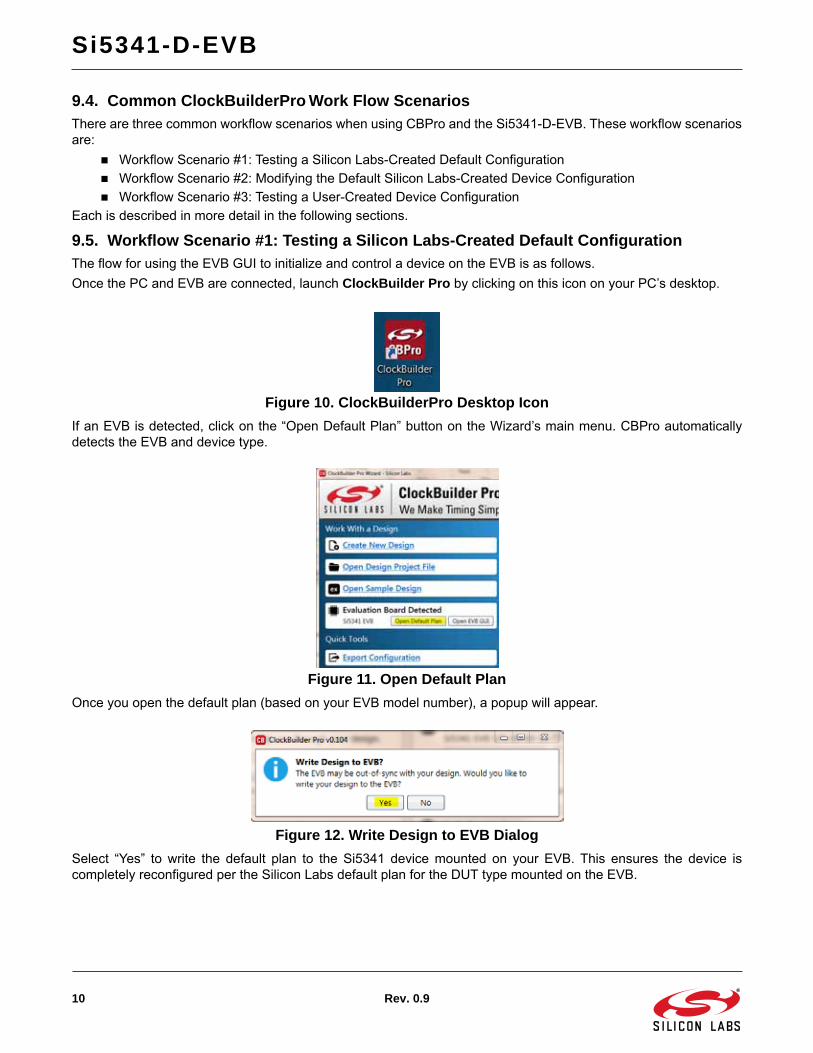
Si5341-D-EVB
10 Rev 09
94 Common ClockBuilderPro Work Flow ScenariosThere are three common workflow scenarios when using CBPro and the Si5341-D-EVB These workflow scenariosare
Workflow Scenario 1 Testing a Silicon Labs-Created Default Configuration
Workflow Scenario 2 Modifying the Default Silicon Labs-Created Device Configuration
Workflow Scenario 3 Testing a User-Created Device Configuration
Each is described in more detail in the following sections
95 Workflow Scenario 1 Testing a Silicon Labs-Created Default ConfigurationThe flow for using the EVB GUI to initialize and control a device on the EVB is as follows
Once the PC and EVB are connected launch ClockBuilder Pro by clicking on this icon on your PCrsquos desktop
Figure 10 ClockBuilderPro Desktop IconIf an EVB is detected click on the ldquoOpen Default Planrdquo button on the Wizardrsquos main menu CBPro automaticallydetects the EVB and device type
Figure 11 Open Default PlanOnce you open the default plan (based on your EVB model number) a popup will appear
Figure 12 Write Design to EVB DialogSelect ldquoYesrdquo to write the default plan to the Si5341 device mounted on your EVB This ensures the device iscompletely reconfigured per the Silicon Labs default plan for the DUT type mounted on the EVB
Si5341-D-EVB
Rev 09 11
Figure 13 Writing Design StatusAfter CBPro writes the default plan to the EVB click on ldquoOpen EVB GUIrdquo as shown below
Figure 14 Open EVB GUIThe EVB GUI will appear Note all power supplies will be set to the values defined in the devicersquos default CBProproject file created by Silicon Labs as shown below
Figure 15 EVB GUI Window
Si5341-D-EVB
12 Rev 09
951 Verify Free-Run Mode OperationAssuming no external clocks have been connected to the INPUT CLOCK differential SMA connectors (labeledldquoINxINxBrdquo) located around the perimeter of the EVB the DUT should now be operating in free-run mode as theDUT will be locked to the crystal in this case
You can run a quick check to determine if the device is powered up and generating output clocks (and consumingpower) by clicking on the Read All button highlighted above and then reviewing the voltage current and powerreadings for each VDDx supply
Note Shutting ldquoOffrdquo then ldquoOnrdquo of the VDD and VDDA supplies will power-down and reset the DUT Every time you dothis to reload the Silicon Labs-created default plan into the DUTrsquos register space you must go back to the Wiz-ardrsquos main menu and select ldquoWrite Design to EVBrdquo
Figure 16 Write Design to EVBFailure to do the step above will cause the device to read in a pre-programmed plan from its non-volatilememory (NVM) However the plan loaded from the NVM may not be the latest plan recommended bySilicon Labs for evaluationAt this point you should verify the presence and frequencies of the output clocks (running to free-run mode fromthe crystal) using appropriate external instrumentation connected to the output clock SMA connectors To verify theoutput clocks are toggling at the correct frequency and signal format click on View Design Report as highlightedbelow
Figure 17 View Design Report
Si5341-D-EVB
Rev 09 13
Your configurationrsquos design report will appear in a new window as shown below Compare the observed outputclocks to the frequencies and formats noted in your default projectrsquos Design Report
Figure 18 Design Report Window952 Verify Locked Mode OperationAssuming you connect the correct input clocks to the EVB (as noted in the Design Report shown above) the DUTon your EVB will be running in ldquolockedrdquo mode
Si5341-D-EVB
14 Rev 09
96 Workflow Scenario 2 Modifying the Default Silicon Labs-Created DeviceConfiguration
To modify the ldquodefaultrdquo configuration using the CBPro Wizard click on Edit Configuration with Wizard
Figure 19 Edit Configuration with WizardYou will now be taken to the Wizardrsquos step-by-step menus to allow you to change any of the default planrsquosoperating configurations
Figure 20 Design Wizard
Si5341-D-EVB
Rev 09 15
Note you can click on the icon on the lower left hand corner of the menu to confirm if your frequency plan is validAfter making your desired changes you can click on Write to EVB to update the DUT to reconfigure your devicereal-time The Design Write status window will appear each time you make a change
Figure 21 Writing Design Status
97 Workflow Scenario 3 Testing a User-Created Device ConfigurationTo test a previously created user configuration open the CBPro Wizard by clicking on the icon on your desktop andthen selecting Open Design Project File
Figure 22 Open Design Project File
Si5341-D-EVB
16 Rev 09
Locate your CBPro design file (slabtimeproj or sitproj file)design file in the Windows file browser
Figure 23 Browse to Project FileSelect Yes when the WRITE DESIGN to EVB popup appears
Figure 24 Write Design to EVB DialogThe progress bar will be launched Once the new design project file has been written to the device verify thepresence and frequencies of your output clocks and other operating configurations using external instrumentation
Si5341-D-EVB
Rev 09 17
98 Exporting the Register Map File for Device Programming by a Host ProcessorYou can also export your configuration to a file format suitable for in-system programming by selecting Export asshown below
Figure 25 Export Register Map FileYou can now write your devicersquos complete configuration to file formats suitable for in-system programming
Figure 26 Export Settings
Si5341-D-EVB
18 Rev 09
10 Writing a New Frequency Plan or Device Configuration to Non-Volatile Memory (OTP)
Note Writing to the device non-volatile memory (OTP) is NOT the same as writing a configuration into the Si5341 using Clock-BuilderPro on the Si5341-D-EB Writing a configuration into the EVB from ClockBuilderPro is done using Si5341 RAMspace and can be done virtually unlimited numbers of times Writing to OTP is limited as described below
Refer to the Si534x8x Family Reference Manuals and device data sheets for information on how to write aconfiguration to the EVB DUTrsquos non-volatile memory (OTP) The OTP can be programmed a maximum of twotimes only Care must be taken to ensure the configuration desired is valid when choosing to write to OTP
11 Si5341-D-EVB Schematic and Bill of Materials (BOM)The Si5341-D-EVB Schematic and Bill of Materials (BOM) can be found online at
httpwwwsilabscomproductsclocksoscillatorspagessi538x-4x-evbaspx
Note Please be aware that the Si5341-D-EB schematic is in OrCad Capture hierarchical format and not in a typical ldquoflatrdquoschematic format
httpwwwsilabscom
Silicon Laboratories Inc400 West Cesar ChavezAustin TX 78701USA
ClockBuilder ProOne-click access to Timing tools documentation software source code libraries amp more Available for Windows and iOS (CBGo only)
wwwsilabscomCBPro
Timing Portfoliowwwsilabscomtiming
SWHWwwwsilabscomCBPro
Qualitywwwsilabscomquality
Support and Communitycommunitysilabscom
DisclaimerSilicon Laboratories intends to provide customers with the latest accurate and in-depth documentation of all peripherals and modules available for system and software implementers using or intending to use the Silicon Laboratories products Characterization data available modules and peripherals memory sizes and memory addresses refer to each specific device and Typical parameters provided can and do vary in different applications Application examples described herein are for illustrative purposes only Silicon Laboratories reserves the right to make changes without further notice and limitation to product information specifications and descriptions herein and does not give warranties as to the accuracy or completeness of the included information Silicon Laboratories shall have no liability for the consequences of use of the information supplied herein This document does not imply or express copyright licenses granted hereunder to design or fabricate any integrated circuits The products are not designed or authorized to be used within any Life Support System without the specific written consent of Silicon Laboratories A Life Support System is any product or system intended to support or sustain life andor health which if it fails can be reasonably expected to result in significant personal injury or death Silicon Laboratories products are not designed or authorized for military applications Silicon Laboratories products shall under no circumstances be used in weapons of mass destruction including (but not limited to) nuclear biological or chemical weapons or missiles capable of delivering such weapons
Trademark InformationSilicon Laboratories Increg Silicon Laboratoriesreg Silicon Labsreg SiLabsreg and the Silicon Labs logoreg Bluegigareg Bluegiga Logoreg Clockbuilderreg CMEMSreg DSPLLreg EFMreg EFM32reg EFR Emberreg Energy Micro Energy Micro logo and combinations thereof the worldrsquos most energy friendly microcontrollers Emberreg EZLinkreg EZRadioreg EZRadioPROreg Geckoreg ISOmodemreg Precision32reg ProSLICreg Simplicity Studioreg SiPHYreg Telegesis the Telegesis Logoreg USBXpressreg and others are trademarks or registered trademarks of Silicon Laborato-ries Inc ARM CORTEX Cortex-M3 and THUMB are trademarks or registered trademarks of ARM Holdings Keil is a registered trademark of ARM Limited All other products or brand names mentioned herein are trademarks of their respective holders
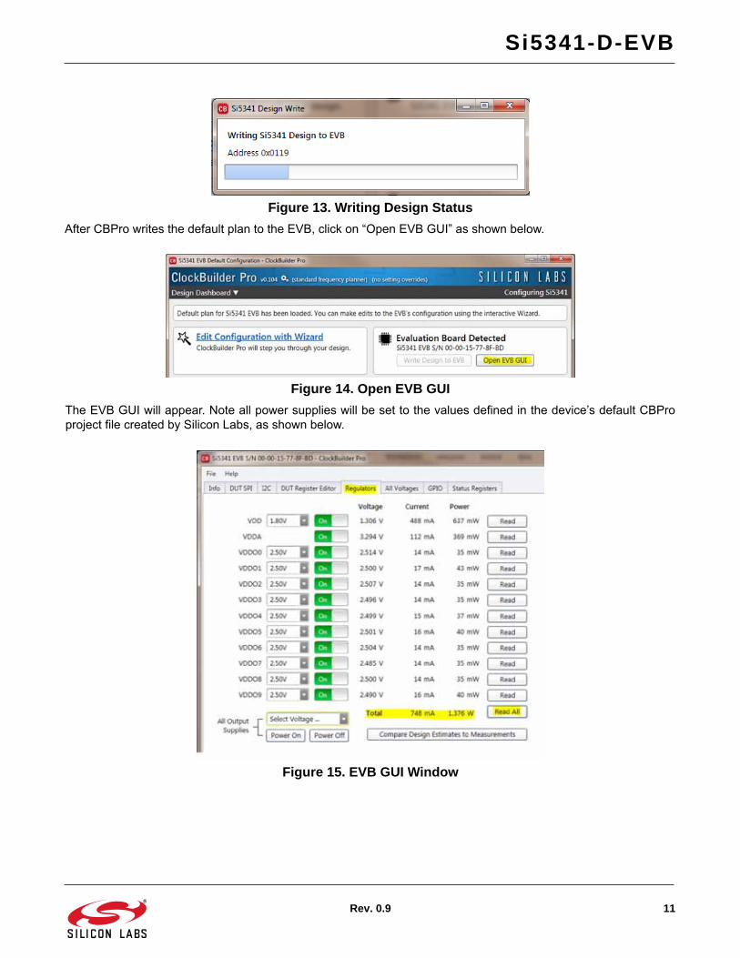
Si5341-D-EVB
Rev 09 11
Figure 13 Writing Design StatusAfter CBPro writes the default plan to the EVB click on ldquoOpen EVB GUIrdquo as shown below
Figure 14 Open EVB GUIThe EVB GUI will appear Note all power supplies will be set to the values defined in the devicersquos default CBProproject file created by Silicon Labs as shown below
Figure 15 EVB GUI Window
Si5341-D-EVB
12 Rev 09
951 Verify Free-Run Mode OperationAssuming no external clocks have been connected to the INPUT CLOCK differential SMA connectors (labeledldquoINxINxBrdquo) located around the perimeter of the EVB the DUT should now be operating in free-run mode as theDUT will be locked to the crystal in this case
You can run a quick check to determine if the device is powered up and generating output clocks (and consumingpower) by clicking on the Read All button highlighted above and then reviewing the voltage current and powerreadings for each VDDx supply
Note Shutting ldquoOffrdquo then ldquoOnrdquo of the VDD and VDDA supplies will power-down and reset the DUT Every time you dothis to reload the Silicon Labs-created default plan into the DUTrsquos register space you must go back to the Wiz-ardrsquos main menu and select ldquoWrite Design to EVBrdquo
Figure 16 Write Design to EVBFailure to do the step above will cause the device to read in a pre-programmed plan from its non-volatilememory (NVM) However the plan loaded from the NVM may not be the latest plan recommended bySilicon Labs for evaluationAt this point you should verify the presence and frequencies of the output clocks (running to free-run mode fromthe crystal) using appropriate external instrumentation connected to the output clock SMA connectors To verify theoutput clocks are toggling at the correct frequency and signal format click on View Design Report as highlightedbelow
Figure 17 View Design Report
Si5341-D-EVB
Rev 09 13
Your configurationrsquos design report will appear in a new window as shown below Compare the observed outputclocks to the frequencies and formats noted in your default projectrsquos Design Report
Figure 18 Design Report Window952 Verify Locked Mode OperationAssuming you connect the correct input clocks to the EVB (as noted in the Design Report shown above) the DUTon your EVB will be running in ldquolockedrdquo mode
Si5341-D-EVB
14 Rev 09
96 Workflow Scenario 2 Modifying the Default Silicon Labs-Created DeviceConfiguration
To modify the ldquodefaultrdquo configuration using the CBPro Wizard click on Edit Configuration with Wizard
Figure 19 Edit Configuration with WizardYou will now be taken to the Wizardrsquos step-by-step menus to allow you to change any of the default planrsquosoperating configurations
Figure 20 Design Wizard
Si5341-D-EVB
Rev 09 15
Note you can click on the icon on the lower left hand corner of the menu to confirm if your frequency plan is validAfter making your desired changes you can click on Write to EVB to update the DUT to reconfigure your devicereal-time The Design Write status window will appear each time you make a change
Figure 21 Writing Design Status
97 Workflow Scenario 3 Testing a User-Created Device ConfigurationTo test a previously created user configuration open the CBPro Wizard by clicking on the icon on your desktop andthen selecting Open Design Project File
Figure 22 Open Design Project File
Si5341-D-EVB
16 Rev 09
Locate your CBPro design file (slabtimeproj or sitproj file)design file in the Windows file browser
Figure 23 Browse to Project FileSelect Yes when the WRITE DESIGN to EVB popup appears
Figure 24 Write Design to EVB DialogThe progress bar will be launched Once the new design project file has been written to the device verify thepresence and frequencies of your output clocks and other operating configurations using external instrumentation
Si5341-D-EVB
Rev 09 17
98 Exporting the Register Map File for Device Programming by a Host ProcessorYou can also export your configuration to a file format suitable for in-system programming by selecting Export asshown below
Figure 25 Export Register Map FileYou can now write your devicersquos complete configuration to file formats suitable for in-system programming
Figure 26 Export Settings
Si5341-D-EVB
18 Rev 09
10 Writing a New Frequency Plan or Device Configuration to Non-Volatile Memory (OTP)
Note Writing to the device non-volatile memory (OTP) is NOT the same as writing a configuration into the Si5341 using Clock-BuilderPro on the Si5341-D-EB Writing a configuration into the EVB from ClockBuilderPro is done using Si5341 RAMspace and can be done virtually unlimited numbers of times Writing to OTP is limited as described below
Refer to the Si534x8x Family Reference Manuals and device data sheets for information on how to write aconfiguration to the EVB DUTrsquos non-volatile memory (OTP) The OTP can be programmed a maximum of twotimes only Care must be taken to ensure the configuration desired is valid when choosing to write to OTP
11 Si5341-D-EVB Schematic and Bill of Materials (BOM)The Si5341-D-EVB Schematic and Bill of Materials (BOM) can be found online at
httpwwwsilabscomproductsclocksoscillatorspagessi538x-4x-evbaspx
Note Please be aware that the Si5341-D-EB schematic is in OrCad Capture hierarchical format and not in a typical ldquoflatrdquoschematic format
httpwwwsilabscom
Silicon Laboratories Inc400 West Cesar ChavezAustin TX 78701USA
ClockBuilder ProOne-click access to Timing tools documentation software source code libraries amp more Available for Windows and iOS (CBGo only)
wwwsilabscomCBPro
Timing Portfoliowwwsilabscomtiming
SWHWwwwsilabscomCBPro
Qualitywwwsilabscomquality
Support and Communitycommunitysilabscom
DisclaimerSilicon Laboratories intends to provide customers with the latest accurate and in-depth documentation of all peripherals and modules available for system and software implementers using or intending to use the Silicon Laboratories products Characterization data available modules and peripherals memory sizes and memory addresses refer to each specific device and Typical parameters provided can and do vary in different applications Application examples described herein are for illustrative purposes only Silicon Laboratories reserves the right to make changes without further notice and limitation to product information specifications and descriptions herein and does not give warranties as to the accuracy or completeness of the included information Silicon Laboratories shall have no liability for the consequences of use of the information supplied herein This document does not imply or express copyright licenses granted hereunder to design or fabricate any integrated circuits The products are not designed or authorized to be used within any Life Support System without the specific written consent of Silicon Laboratories A Life Support System is any product or system intended to support or sustain life andor health which if it fails can be reasonably expected to result in significant personal injury or death Silicon Laboratories products are not designed or authorized for military applications Silicon Laboratories products shall under no circumstances be used in weapons of mass destruction including (but not limited to) nuclear biological or chemical weapons or missiles capable of delivering such weapons
Trademark InformationSilicon Laboratories Increg Silicon Laboratoriesreg Silicon Labsreg SiLabsreg and the Silicon Labs logoreg Bluegigareg Bluegiga Logoreg Clockbuilderreg CMEMSreg DSPLLreg EFMreg EFM32reg EFR Emberreg Energy Micro Energy Micro logo and combinations thereof the worldrsquos most energy friendly microcontrollers Emberreg EZLinkreg EZRadioreg EZRadioPROreg Geckoreg ISOmodemreg Precision32reg ProSLICreg Simplicity Studioreg SiPHYreg Telegesis the Telegesis Logoreg USBXpressreg and others are trademarks or registered trademarks of Silicon Laborato-ries Inc ARM CORTEX Cortex-M3 and THUMB are trademarks or registered trademarks of ARM Holdings Keil is a registered trademark of ARM Limited All other products or brand names mentioned herein are trademarks of their respective holders
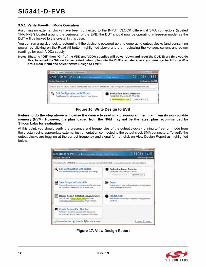
Si5341-D-EVB
12 Rev 09
951 Verify Free-Run Mode OperationAssuming no external clocks have been connected to the INPUT CLOCK differential SMA connectors (labeledldquoINxINxBrdquo) located around the perimeter of the EVB the DUT should now be operating in free-run mode as theDUT will be locked to the crystal in this case
You can run a quick check to determine if the device is powered up and generating output clocks (and consumingpower) by clicking on the Read All button highlighted above and then reviewing the voltage current and powerreadings for each VDDx supply
Note Shutting ldquoOffrdquo then ldquoOnrdquo of the VDD and VDDA supplies will power-down and reset the DUT Every time you dothis to reload the Silicon Labs-created default plan into the DUTrsquos register space you must go back to the Wiz-ardrsquos main menu and select ldquoWrite Design to EVBrdquo
Figure 16 Write Design to EVBFailure to do the step above will cause the device to read in a pre-programmed plan from its non-volatilememory (NVM) However the plan loaded from the NVM may not be the latest plan recommended bySilicon Labs for evaluationAt this point you should verify the presence and frequencies of the output clocks (running to free-run mode fromthe crystal) using appropriate external instrumentation connected to the output clock SMA connectors To verify theoutput clocks are toggling at the correct frequency and signal format click on View Design Report as highlightedbelow
Figure 17 View Design Report
Si5341-D-EVB
Rev 09 13
Your configurationrsquos design report will appear in a new window as shown below Compare the observed outputclocks to the frequencies and formats noted in your default projectrsquos Design Report
Figure 18 Design Report Window952 Verify Locked Mode OperationAssuming you connect the correct input clocks to the EVB (as noted in the Design Report shown above) the DUTon your EVB will be running in ldquolockedrdquo mode
Si5341-D-EVB
14 Rev 09
96 Workflow Scenario 2 Modifying the Default Silicon Labs-Created DeviceConfiguration
To modify the ldquodefaultrdquo configuration using the CBPro Wizard click on Edit Configuration with Wizard
Figure 19 Edit Configuration with WizardYou will now be taken to the Wizardrsquos step-by-step menus to allow you to change any of the default planrsquosoperating configurations
Figure 20 Design Wizard
Si5341-D-EVB
Rev 09 15
Note you can click on the icon on the lower left hand corner of the menu to confirm if your frequency plan is validAfter making your desired changes you can click on Write to EVB to update the DUT to reconfigure your devicereal-time The Design Write status window will appear each time you make a change
Figure 21 Writing Design Status
97 Workflow Scenario 3 Testing a User-Created Device ConfigurationTo test a previously created user configuration open the CBPro Wizard by clicking on the icon on your desktop andthen selecting Open Design Project File
Figure 22 Open Design Project File
Si5341-D-EVB
16 Rev 09
Locate your CBPro design file (slabtimeproj or sitproj file)design file in the Windows file browser
Figure 23 Browse to Project FileSelect Yes when the WRITE DESIGN to EVB popup appears
Figure 24 Write Design to EVB DialogThe progress bar will be launched Once the new design project file has been written to the device verify thepresence and frequencies of your output clocks and other operating configurations using external instrumentation
Si5341-D-EVB
Rev 09 17
98 Exporting the Register Map File for Device Programming by a Host ProcessorYou can also export your configuration to a file format suitable for in-system programming by selecting Export asshown below
Figure 25 Export Register Map FileYou can now write your devicersquos complete configuration to file formats suitable for in-system programming
Figure 26 Export Settings
Si5341-D-EVB
18 Rev 09
10 Writing a New Frequency Plan or Device Configuration to Non-Volatile Memory (OTP)
Note Writing to the device non-volatile memory (OTP) is NOT the same as writing a configuration into the Si5341 using Clock-BuilderPro on the Si5341-D-EB Writing a configuration into the EVB from ClockBuilderPro is done using Si5341 RAMspace and can be done virtually unlimited numbers of times Writing to OTP is limited as described below
Refer to the Si534x8x Family Reference Manuals and device data sheets for information on how to write aconfiguration to the EVB DUTrsquos non-volatile memory (OTP) The OTP can be programmed a maximum of twotimes only Care must be taken to ensure the configuration desired is valid when choosing to write to OTP
11 Si5341-D-EVB Schematic and Bill of Materials (BOM)The Si5341-D-EVB Schematic and Bill of Materials (BOM) can be found online at
httpwwwsilabscomproductsclocksoscillatorspagessi538x-4x-evbaspx
Note Please be aware that the Si5341-D-EB schematic is in OrCad Capture hierarchical format and not in a typical ldquoflatrdquoschematic format
httpwwwsilabscom
Silicon Laboratories Inc400 West Cesar ChavezAustin TX 78701USA
ClockBuilder ProOne-click access to Timing tools documentation software source code libraries amp more Available for Windows and iOS (CBGo only)
wwwsilabscomCBPro
Timing Portfoliowwwsilabscomtiming
SWHWwwwsilabscomCBPro
Qualitywwwsilabscomquality
Support and Communitycommunitysilabscom
DisclaimerSilicon Laboratories intends to provide customers with the latest accurate and in-depth documentation of all peripherals and modules available for system and software implementers using or intending to use the Silicon Laboratories products Characterization data available modules and peripherals memory sizes and memory addresses refer to each specific device and Typical parameters provided can and do vary in different applications Application examples described herein are for illustrative purposes only Silicon Laboratories reserves the right to make changes without further notice and limitation to product information specifications and descriptions herein and does not give warranties as to the accuracy or completeness of the included information Silicon Laboratories shall have no liability for the consequences of use of the information supplied herein This document does not imply or express copyright licenses granted hereunder to design or fabricate any integrated circuits The products are not designed or authorized to be used within any Life Support System without the specific written consent of Silicon Laboratories A Life Support System is any product or system intended to support or sustain life andor health which if it fails can be reasonably expected to result in significant personal injury or death Silicon Laboratories products are not designed or authorized for military applications Silicon Laboratories products shall under no circumstances be used in weapons of mass destruction including (but not limited to) nuclear biological or chemical weapons or missiles capable of delivering such weapons
Trademark InformationSilicon Laboratories Increg Silicon Laboratoriesreg Silicon Labsreg SiLabsreg and the Silicon Labs logoreg Bluegigareg Bluegiga Logoreg Clockbuilderreg CMEMSreg DSPLLreg EFMreg EFM32reg EFR Emberreg Energy Micro Energy Micro logo and combinations thereof the worldrsquos most energy friendly microcontrollers Emberreg EZLinkreg EZRadioreg EZRadioPROreg Geckoreg ISOmodemreg Precision32reg ProSLICreg Simplicity Studioreg SiPHYreg Telegesis the Telegesis Logoreg USBXpressreg and others are trademarks or registered trademarks of Silicon Laborato-ries Inc ARM CORTEX Cortex-M3 and THUMB are trademarks or registered trademarks of ARM Holdings Keil is a registered trademark of ARM Limited All other products or brand names mentioned herein are trademarks of their respective holders
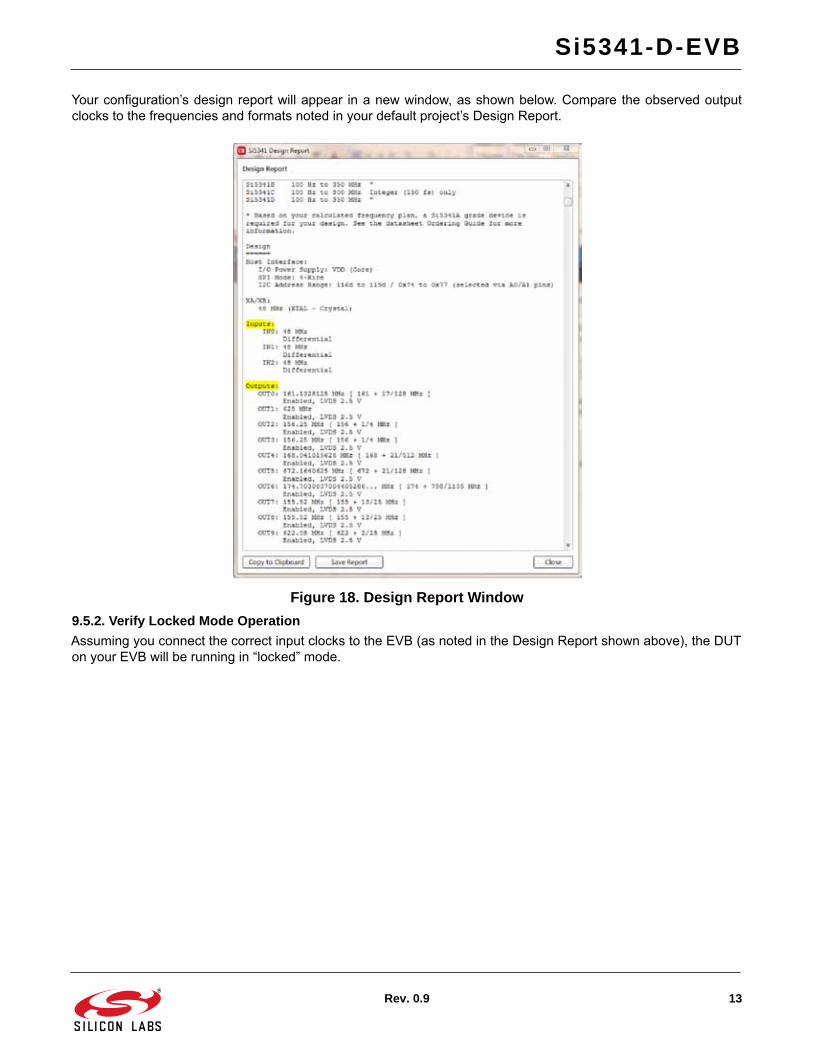
Si5341-D-EVB
Rev 09 13
Your configurationrsquos design report will appear in a new window as shown below Compare the observed outputclocks to the frequencies and formats noted in your default projectrsquos Design Report
Figure 18 Design Report Window952 Verify Locked Mode OperationAssuming you connect the correct input clocks to the EVB (as noted in the Design Report shown above) the DUTon your EVB will be running in ldquolockedrdquo mode
Si5341-D-EVB
14 Rev 09
96 Workflow Scenario 2 Modifying the Default Silicon Labs-Created DeviceConfiguration
To modify the ldquodefaultrdquo configuration using the CBPro Wizard click on Edit Configuration with Wizard
Figure 19 Edit Configuration with WizardYou will now be taken to the Wizardrsquos step-by-step menus to allow you to change any of the default planrsquosoperating configurations
Figure 20 Design Wizard
Si5341-D-EVB
Rev 09 15
Note you can click on the icon on the lower left hand corner of the menu to confirm if your frequency plan is validAfter making your desired changes you can click on Write to EVB to update the DUT to reconfigure your devicereal-time The Design Write status window will appear each time you make a change
Figure 21 Writing Design Status
97 Workflow Scenario 3 Testing a User-Created Device ConfigurationTo test a previously created user configuration open the CBPro Wizard by clicking on the icon on your desktop andthen selecting Open Design Project File
Figure 22 Open Design Project File
Si5341-D-EVB
16 Rev 09
Locate your CBPro design file (slabtimeproj or sitproj file)design file in the Windows file browser
Figure 23 Browse to Project FileSelect Yes when the WRITE DESIGN to EVB popup appears
Figure 24 Write Design to EVB DialogThe progress bar will be launched Once the new design project file has been written to the device verify thepresence and frequencies of your output clocks and other operating configurations using external instrumentation
Si5341-D-EVB
Rev 09 17
98 Exporting the Register Map File for Device Programming by a Host ProcessorYou can also export your configuration to a file format suitable for in-system programming by selecting Export asshown below
Figure 25 Export Register Map FileYou can now write your devicersquos complete configuration to file formats suitable for in-system programming
Figure 26 Export Settings
Si5341-D-EVB
18 Rev 09
10 Writing a New Frequency Plan or Device Configuration to Non-Volatile Memory (OTP)
Note Writing to the device non-volatile memory (OTP) is NOT the same as writing a configuration into the Si5341 using Clock-BuilderPro on the Si5341-D-EB Writing a configuration into the EVB from ClockBuilderPro is done using Si5341 RAMspace and can be done virtually unlimited numbers of times Writing to OTP is limited as described below
Refer to the Si534x8x Family Reference Manuals and device data sheets for information on how to write aconfiguration to the EVB DUTrsquos non-volatile memory (OTP) The OTP can be programmed a maximum of twotimes only Care must be taken to ensure the configuration desired is valid when choosing to write to OTP
11 Si5341-D-EVB Schematic and Bill of Materials (BOM)The Si5341-D-EVB Schematic and Bill of Materials (BOM) can be found online at
httpwwwsilabscomproductsclocksoscillatorspagessi538x-4x-evbaspx
Note Please be aware that the Si5341-D-EB schematic is in OrCad Capture hierarchical format and not in a typical ldquoflatrdquoschematic format
httpwwwsilabscom
Silicon Laboratories Inc400 West Cesar ChavezAustin TX 78701USA
ClockBuilder ProOne-click access to Timing tools documentation software source code libraries amp more Available for Windows and iOS (CBGo only)
wwwsilabscomCBPro
Timing Portfoliowwwsilabscomtiming
SWHWwwwsilabscomCBPro
Qualitywwwsilabscomquality
Support and Communitycommunitysilabscom
DisclaimerSilicon Laboratories intends to provide customers with the latest accurate and in-depth documentation of all peripherals and modules available for system and software implementers using or intending to use the Silicon Laboratories products Characterization data available modules and peripherals memory sizes and memory addresses refer to each specific device and Typical parameters provided can and do vary in different applications Application examples described herein are for illustrative purposes only Silicon Laboratories reserves the right to make changes without further notice and limitation to product information specifications and descriptions herein and does not give warranties as to the accuracy or completeness of the included information Silicon Laboratories shall have no liability for the consequences of use of the information supplied herein This document does not imply or express copyright licenses granted hereunder to design or fabricate any integrated circuits The products are not designed or authorized to be used within any Life Support System without the specific written consent of Silicon Laboratories A Life Support System is any product or system intended to support or sustain life andor health which if it fails can be reasonably expected to result in significant personal injury or death Silicon Laboratories products are not designed or authorized for military applications Silicon Laboratories products shall under no circumstances be used in weapons of mass destruction including (but not limited to) nuclear biological or chemical weapons or missiles capable of delivering such weapons
Trademark InformationSilicon Laboratories Increg Silicon Laboratoriesreg Silicon Labsreg SiLabsreg and the Silicon Labs logoreg Bluegigareg Bluegiga Logoreg Clockbuilderreg CMEMSreg DSPLLreg EFMreg EFM32reg EFR Emberreg Energy Micro Energy Micro logo and combinations thereof the worldrsquos most energy friendly microcontrollers Emberreg EZLinkreg EZRadioreg EZRadioPROreg Geckoreg ISOmodemreg Precision32reg ProSLICreg Simplicity Studioreg SiPHYreg Telegesis the Telegesis Logoreg USBXpressreg and others are trademarks or registered trademarks of Silicon Laborato-ries Inc ARM CORTEX Cortex-M3 and THUMB are trademarks or registered trademarks of ARM Holdings Keil is a registered trademark of ARM Limited All other products or brand names mentioned herein are trademarks of their respective holders
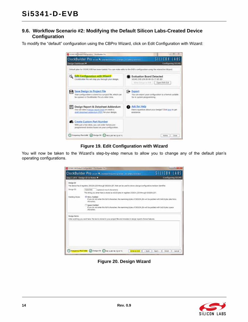
Si5341-D-EVB
14 Rev 09
96 Workflow Scenario 2 Modifying the Default Silicon Labs-Created DeviceConfiguration
To modify the ldquodefaultrdquo configuration using the CBPro Wizard click on Edit Configuration with Wizard
Figure 19 Edit Configuration with WizardYou will now be taken to the Wizardrsquos step-by-step menus to allow you to change any of the default planrsquosoperating configurations
Figure 20 Design Wizard
Si5341-D-EVB
Rev 09 15
Note you can click on the icon on the lower left hand corner of the menu to confirm if your frequency plan is validAfter making your desired changes you can click on Write to EVB to update the DUT to reconfigure your devicereal-time The Design Write status window will appear each time you make a change
Figure 21 Writing Design Status
97 Workflow Scenario 3 Testing a User-Created Device ConfigurationTo test a previously created user configuration open the CBPro Wizard by clicking on the icon on your desktop andthen selecting Open Design Project File
Figure 22 Open Design Project File
Si5341-D-EVB
16 Rev 09
Locate your CBPro design file (slabtimeproj or sitproj file)design file in the Windows file browser
Figure 23 Browse to Project FileSelect Yes when the WRITE DESIGN to EVB popup appears
Figure 24 Write Design to EVB DialogThe progress bar will be launched Once the new design project file has been written to the device verify thepresence and frequencies of your output clocks and other operating configurations using external instrumentation
Si5341-D-EVB
Rev 09 17
98 Exporting the Register Map File for Device Programming by a Host ProcessorYou can also export your configuration to a file format suitable for in-system programming by selecting Export asshown below
Figure 25 Export Register Map FileYou can now write your devicersquos complete configuration to file formats suitable for in-system programming
Figure 26 Export Settings
Si5341-D-EVB
18 Rev 09
10 Writing a New Frequency Plan or Device Configuration to Non-Volatile Memory (OTP)
Note Writing to the device non-volatile memory (OTP) is NOT the same as writing a configuration into the Si5341 using Clock-BuilderPro on the Si5341-D-EB Writing a configuration into the EVB from ClockBuilderPro is done using Si5341 RAMspace and can be done virtually unlimited numbers of times Writing to OTP is limited as described below
Refer to the Si534x8x Family Reference Manuals and device data sheets for information on how to write aconfiguration to the EVB DUTrsquos non-volatile memory (OTP) The OTP can be programmed a maximum of twotimes only Care must be taken to ensure the configuration desired is valid when choosing to write to OTP
11 Si5341-D-EVB Schematic and Bill of Materials (BOM)The Si5341-D-EVB Schematic and Bill of Materials (BOM) can be found online at
httpwwwsilabscomproductsclocksoscillatorspagessi538x-4x-evbaspx
Note Please be aware that the Si5341-D-EB schematic is in OrCad Capture hierarchical format and not in a typical ldquoflatrdquoschematic format
httpwwwsilabscom
Silicon Laboratories Inc400 West Cesar ChavezAustin TX 78701USA
ClockBuilder ProOne-click access to Timing tools documentation software source code libraries amp more Available for Windows and iOS (CBGo only)
wwwsilabscomCBPro
Timing Portfoliowwwsilabscomtiming
SWHWwwwsilabscomCBPro
Qualitywwwsilabscomquality
Support and Communitycommunitysilabscom
DisclaimerSilicon Laboratories intends to provide customers with the latest accurate and in-depth documentation of all peripherals and modules available for system and software implementers using or intending to use the Silicon Laboratories products Characterization data available modules and peripherals memory sizes and memory addresses refer to each specific device and Typical parameters provided can and do vary in different applications Application examples described herein are for illustrative purposes only Silicon Laboratories reserves the right to make changes without further notice and limitation to product information specifications and descriptions herein and does not give warranties as to the accuracy or completeness of the included information Silicon Laboratories shall have no liability for the consequences of use of the information supplied herein This document does not imply or express copyright licenses granted hereunder to design or fabricate any integrated circuits The products are not designed or authorized to be used within any Life Support System without the specific written consent of Silicon Laboratories A Life Support System is any product or system intended to support or sustain life andor health which if it fails can be reasonably expected to result in significant personal injury or death Silicon Laboratories products are not designed or authorized for military applications Silicon Laboratories products shall under no circumstances be used in weapons of mass destruction including (but not limited to) nuclear biological or chemical weapons or missiles capable of delivering such weapons
Trademark InformationSilicon Laboratories Increg Silicon Laboratoriesreg Silicon Labsreg SiLabsreg and the Silicon Labs logoreg Bluegigareg Bluegiga Logoreg Clockbuilderreg CMEMSreg DSPLLreg EFMreg EFM32reg EFR Emberreg Energy Micro Energy Micro logo and combinations thereof the worldrsquos most energy friendly microcontrollers Emberreg EZLinkreg EZRadioreg EZRadioPROreg Geckoreg ISOmodemreg Precision32reg ProSLICreg Simplicity Studioreg SiPHYreg Telegesis the Telegesis Logoreg USBXpressreg and others are trademarks or registered trademarks of Silicon Laborato-ries Inc ARM CORTEX Cortex-M3 and THUMB are trademarks or registered trademarks of ARM Holdings Keil is a registered trademark of ARM Limited All other products or brand names mentioned herein are trademarks of their respective holders
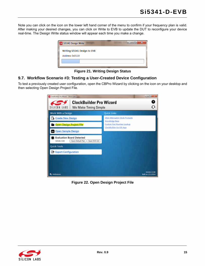
Si5341-D-EVB
Rev 09 15
Note you can click on the icon on the lower left hand corner of the menu to confirm if your frequency plan is validAfter making your desired changes you can click on Write to EVB to update the DUT to reconfigure your devicereal-time The Design Write status window will appear each time you make a change
Figure 21 Writing Design Status
97 Workflow Scenario 3 Testing a User-Created Device ConfigurationTo test a previously created user configuration open the CBPro Wizard by clicking on the icon on your desktop andthen selecting Open Design Project File
Figure 22 Open Design Project File
Si5341-D-EVB
16 Rev 09
Locate your CBPro design file (slabtimeproj or sitproj file)design file in the Windows file browser
Figure 23 Browse to Project FileSelect Yes when the WRITE DESIGN to EVB popup appears
Figure 24 Write Design to EVB DialogThe progress bar will be launched Once the new design project file has been written to the device verify thepresence and frequencies of your output clocks and other operating configurations using external instrumentation
Si5341-D-EVB
Rev 09 17
98 Exporting the Register Map File for Device Programming by a Host ProcessorYou can also export your configuration to a file format suitable for in-system programming by selecting Export asshown below
Figure 25 Export Register Map FileYou can now write your devicersquos complete configuration to file formats suitable for in-system programming
Figure 26 Export Settings
Si5341-D-EVB
18 Rev 09
10 Writing a New Frequency Plan or Device Configuration to Non-Volatile Memory (OTP)
Note Writing to the device non-volatile memory (OTP) is NOT the same as writing a configuration into the Si5341 using Clock-BuilderPro on the Si5341-D-EB Writing a configuration into the EVB from ClockBuilderPro is done using Si5341 RAMspace and can be done virtually unlimited numbers of times Writing to OTP is limited as described below
Refer to the Si534x8x Family Reference Manuals and device data sheets for information on how to write aconfiguration to the EVB DUTrsquos non-volatile memory (OTP) The OTP can be programmed a maximum of twotimes only Care must be taken to ensure the configuration desired is valid when choosing to write to OTP
11 Si5341-D-EVB Schematic and Bill of Materials (BOM)The Si5341-D-EVB Schematic and Bill of Materials (BOM) can be found online at
httpwwwsilabscomproductsclocksoscillatorspagessi538x-4x-evbaspx
Note Please be aware that the Si5341-D-EB schematic is in OrCad Capture hierarchical format and not in a typical ldquoflatrdquoschematic format
httpwwwsilabscom
Silicon Laboratories Inc400 West Cesar ChavezAustin TX 78701USA
ClockBuilder ProOne-click access to Timing tools documentation software source code libraries amp more Available for Windows and iOS (CBGo only)
wwwsilabscomCBPro
Timing Portfoliowwwsilabscomtiming
SWHWwwwsilabscomCBPro
Qualitywwwsilabscomquality
Support and Communitycommunitysilabscom
DisclaimerSilicon Laboratories intends to provide customers with the latest accurate and in-depth documentation of all peripherals and modules available for system and software implementers using or intending to use the Silicon Laboratories products Characterization data available modules and peripherals memory sizes and memory addresses refer to each specific device and Typical parameters provided can and do vary in different applications Application examples described herein are for illustrative purposes only Silicon Laboratories reserves the right to make changes without further notice and limitation to product information specifications and descriptions herein and does not give warranties as to the accuracy or completeness of the included information Silicon Laboratories shall have no liability for the consequences of use of the information supplied herein This document does not imply or express copyright licenses granted hereunder to design or fabricate any integrated circuits The products are not designed or authorized to be used within any Life Support System without the specific written consent of Silicon Laboratories A Life Support System is any product or system intended to support or sustain life andor health which if it fails can be reasonably expected to result in significant personal injury or death Silicon Laboratories products are not designed or authorized for military applications Silicon Laboratories products shall under no circumstances be used in weapons of mass destruction including (but not limited to) nuclear biological or chemical weapons or missiles capable of delivering such weapons
Trademark InformationSilicon Laboratories Increg Silicon Laboratoriesreg Silicon Labsreg SiLabsreg and the Silicon Labs logoreg Bluegigareg Bluegiga Logoreg Clockbuilderreg CMEMSreg DSPLLreg EFMreg EFM32reg EFR Emberreg Energy Micro Energy Micro logo and combinations thereof the worldrsquos most energy friendly microcontrollers Emberreg EZLinkreg EZRadioreg EZRadioPROreg Geckoreg ISOmodemreg Precision32reg ProSLICreg Simplicity Studioreg SiPHYreg Telegesis the Telegesis Logoreg USBXpressreg and others are trademarks or registered trademarks of Silicon Laborato-ries Inc ARM CORTEX Cortex-M3 and THUMB are trademarks or registered trademarks of ARM Holdings Keil is a registered trademark of ARM Limited All other products or brand names mentioned herein are trademarks of their respective holders
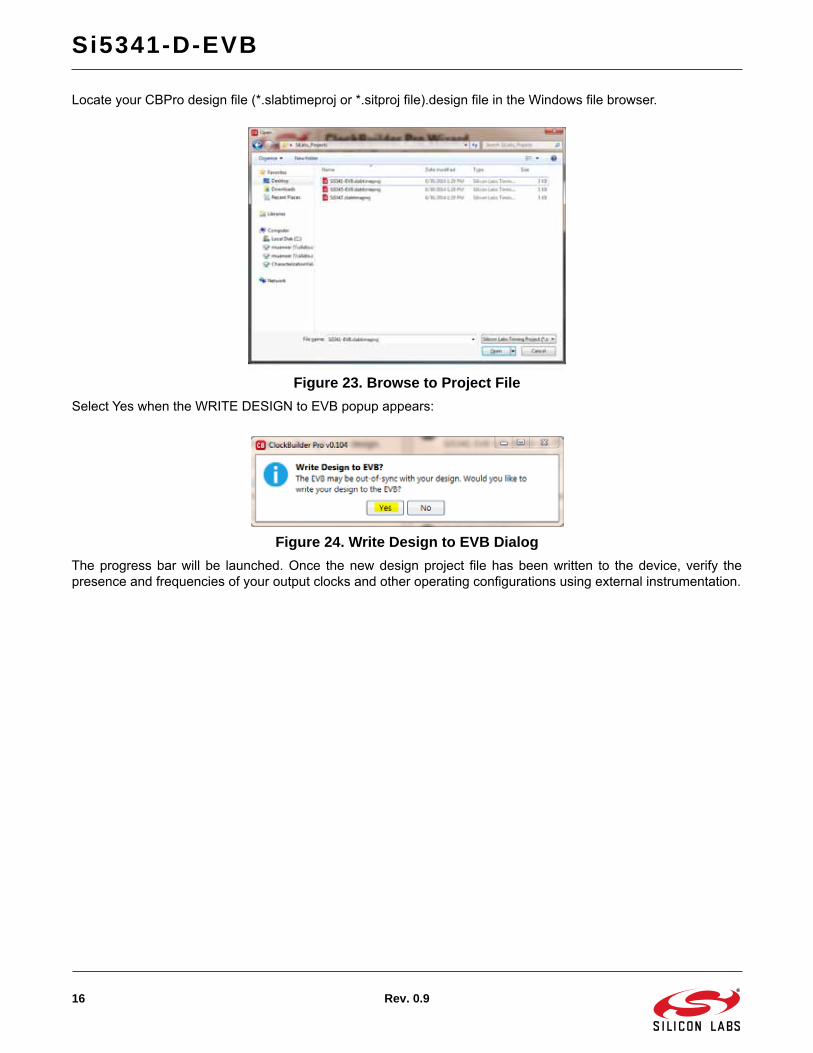
Si5341-D-EVB
16 Rev 09
Locate your CBPro design file (slabtimeproj or sitproj file)design file in the Windows file browser
Figure 23 Browse to Project FileSelect Yes when the WRITE DESIGN to EVB popup appears
Figure 24 Write Design to EVB DialogThe progress bar will be launched Once the new design project file has been written to the device verify thepresence and frequencies of your output clocks and other operating configurations using external instrumentation
Si5341-D-EVB
Rev 09 17
98 Exporting the Register Map File for Device Programming by a Host ProcessorYou can also export your configuration to a file format suitable for in-system programming by selecting Export asshown below
Figure 25 Export Register Map FileYou can now write your devicersquos complete configuration to file formats suitable for in-system programming
Figure 26 Export Settings
Si5341-D-EVB
18 Rev 09
10 Writing a New Frequency Plan or Device Configuration to Non-Volatile Memory (OTP)
Note Writing to the device non-volatile memory (OTP) is NOT the same as writing a configuration into the Si5341 using Clock-BuilderPro on the Si5341-D-EB Writing a configuration into the EVB from ClockBuilderPro is done using Si5341 RAMspace and can be done virtually unlimited numbers of times Writing to OTP is limited as described below
Refer to the Si534x8x Family Reference Manuals and device data sheets for information on how to write aconfiguration to the EVB DUTrsquos non-volatile memory (OTP) The OTP can be programmed a maximum of twotimes only Care must be taken to ensure the configuration desired is valid when choosing to write to OTP
11 Si5341-D-EVB Schematic and Bill of Materials (BOM)The Si5341-D-EVB Schematic and Bill of Materials (BOM) can be found online at
httpwwwsilabscomproductsclocksoscillatorspagessi538x-4x-evbaspx
Note Please be aware that the Si5341-D-EB schematic is in OrCad Capture hierarchical format and not in a typical ldquoflatrdquoschematic format
httpwwwsilabscom
Silicon Laboratories Inc400 West Cesar ChavezAustin TX 78701USA
ClockBuilder ProOne-click access to Timing tools documentation software source code libraries amp more Available for Windows and iOS (CBGo only)
wwwsilabscomCBPro
Timing Portfoliowwwsilabscomtiming
SWHWwwwsilabscomCBPro
Qualitywwwsilabscomquality
Support and Communitycommunitysilabscom
DisclaimerSilicon Laboratories intends to provide customers with the latest accurate and in-depth documentation of all peripherals and modules available for system and software implementers using or intending to use the Silicon Laboratories products Characterization data available modules and peripherals memory sizes and memory addresses refer to each specific device and Typical parameters provided can and do vary in different applications Application examples described herein are for illustrative purposes only Silicon Laboratories reserves the right to make changes without further notice and limitation to product information specifications and descriptions herein and does not give warranties as to the accuracy or completeness of the included information Silicon Laboratories shall have no liability for the consequences of use of the information supplied herein This document does not imply or express copyright licenses granted hereunder to design or fabricate any integrated circuits The products are not designed or authorized to be used within any Life Support System without the specific written consent of Silicon Laboratories A Life Support System is any product or system intended to support or sustain life andor health which if it fails can be reasonably expected to result in significant personal injury or death Silicon Laboratories products are not designed or authorized for military applications Silicon Laboratories products shall under no circumstances be used in weapons of mass destruction including (but not limited to) nuclear biological or chemical weapons or missiles capable of delivering such weapons
Trademark InformationSilicon Laboratories Increg Silicon Laboratoriesreg Silicon Labsreg SiLabsreg and the Silicon Labs logoreg Bluegigareg Bluegiga Logoreg Clockbuilderreg CMEMSreg DSPLLreg EFMreg EFM32reg EFR Emberreg Energy Micro Energy Micro logo and combinations thereof the worldrsquos most energy friendly microcontrollers Emberreg EZLinkreg EZRadioreg EZRadioPROreg Geckoreg ISOmodemreg Precision32reg ProSLICreg Simplicity Studioreg SiPHYreg Telegesis the Telegesis Logoreg USBXpressreg and others are trademarks or registered trademarks of Silicon Laborato-ries Inc ARM CORTEX Cortex-M3 and THUMB are trademarks or registered trademarks of ARM Holdings Keil is a registered trademark of ARM Limited All other products or brand names mentioned herein are trademarks of their respective holders
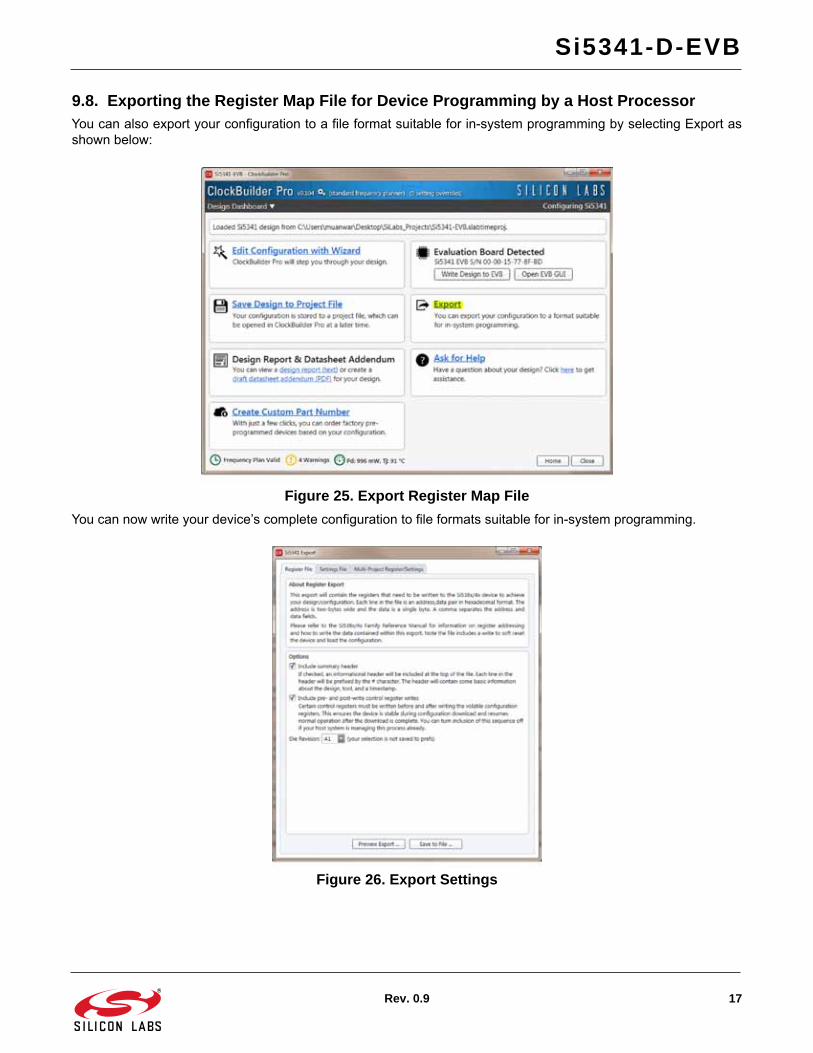
Si5341-D-EVB
Rev 09 17
98 Exporting the Register Map File for Device Programming by a Host ProcessorYou can also export your configuration to a file format suitable for in-system programming by selecting Export asshown below
Figure 25 Export Register Map FileYou can now write your devicersquos complete configuration to file formats suitable for in-system programming
Figure 26 Export Settings
Si5341-D-EVB
18 Rev 09
10 Writing a New Frequency Plan or Device Configuration to Non-Volatile Memory (OTP)
Note Writing to the device non-volatile memory (OTP) is NOT the same as writing a configuration into the Si5341 using Clock-BuilderPro on the Si5341-D-EB Writing a configuration into the EVB from ClockBuilderPro is done using Si5341 RAMspace and can be done virtually unlimited numbers of times Writing to OTP is limited as described below
Refer to the Si534x8x Family Reference Manuals and device data sheets for information on how to write aconfiguration to the EVB DUTrsquos non-volatile memory (OTP) The OTP can be programmed a maximum of twotimes only Care must be taken to ensure the configuration desired is valid when choosing to write to OTP
11 Si5341-D-EVB Schematic and Bill of Materials (BOM)The Si5341-D-EVB Schematic and Bill of Materials (BOM) can be found online at
httpwwwsilabscomproductsclocksoscillatorspagessi538x-4x-evbaspx
Note Please be aware that the Si5341-D-EB schematic is in OrCad Capture hierarchical format and not in a typical ldquoflatrdquoschematic format
httpwwwsilabscom
Silicon Laboratories Inc400 West Cesar ChavezAustin TX 78701USA
ClockBuilder ProOne-click access to Timing tools documentation software source code libraries amp more Available for Windows and iOS (CBGo only)
wwwsilabscomCBPro
Timing Portfoliowwwsilabscomtiming
SWHWwwwsilabscomCBPro
Qualitywwwsilabscomquality
Support and Communitycommunitysilabscom
DisclaimerSilicon Laboratories intends to provide customers with the latest accurate and in-depth documentation of all peripherals and modules available for system and software implementers using or intending to use the Silicon Laboratories products Characterization data available modules and peripherals memory sizes and memory addresses refer to each specific device and Typical parameters provided can and do vary in different applications Application examples described herein are for illustrative purposes only Silicon Laboratories reserves the right to make changes without further notice and limitation to product information specifications and descriptions herein and does not give warranties as to the accuracy or completeness of the included information Silicon Laboratories shall have no liability for the consequences of use of the information supplied herein This document does not imply or express copyright licenses granted hereunder to design or fabricate any integrated circuits The products are not designed or authorized to be used within any Life Support System without the specific written consent of Silicon Laboratories A Life Support System is any product or system intended to support or sustain life andor health which if it fails can be reasonably expected to result in significant personal injury or death Silicon Laboratories products are not designed or authorized for military applications Silicon Laboratories products shall under no circumstances be used in weapons of mass destruction including (but not limited to) nuclear biological or chemical weapons or missiles capable of delivering such weapons
Trademark InformationSilicon Laboratories Increg Silicon Laboratoriesreg Silicon Labsreg SiLabsreg and the Silicon Labs logoreg Bluegigareg Bluegiga Logoreg Clockbuilderreg CMEMSreg DSPLLreg EFMreg EFM32reg EFR Emberreg Energy Micro Energy Micro logo and combinations thereof the worldrsquos most energy friendly microcontrollers Emberreg EZLinkreg EZRadioreg EZRadioPROreg Geckoreg ISOmodemreg Precision32reg ProSLICreg Simplicity Studioreg SiPHYreg Telegesis the Telegesis Logoreg USBXpressreg and others are trademarks or registered trademarks of Silicon Laborato-ries Inc ARM CORTEX Cortex-M3 and THUMB are trademarks or registered trademarks of ARM Holdings Keil is a registered trademark of ARM Limited All other products or brand names mentioned herein are trademarks of their respective holders
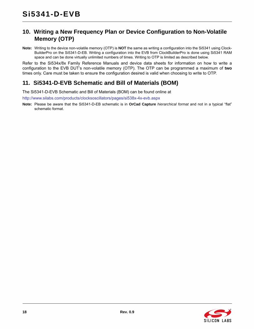
Si5341-D-EVB
18 Rev 09
10 Writing a New Frequency Plan or Device Configuration to Non-Volatile Memory (OTP)
Note Writing to the device non-volatile memory (OTP) is NOT the same as writing a configuration into the Si5341 using Clock-BuilderPro on the Si5341-D-EB Writing a configuration into the EVB from ClockBuilderPro is done using Si5341 RAMspace and can be done virtually unlimited numbers of times Writing to OTP is limited as described below
Refer to the Si534x8x Family Reference Manuals and device data sheets for information on how to write aconfiguration to the EVB DUTrsquos non-volatile memory (OTP) The OTP can be programmed a maximum of twotimes only Care must be taken to ensure the configuration desired is valid when choosing to write to OTP
11 Si5341-D-EVB Schematic and Bill of Materials (BOM)The Si5341-D-EVB Schematic and Bill of Materials (BOM) can be found online at
httpwwwsilabscomproductsclocksoscillatorspagessi538x-4x-evbaspx
Note Please be aware that the Si5341-D-EB schematic is in OrCad Capture hierarchical format and not in a typical ldquoflatrdquoschematic format
httpwwwsilabscom
Silicon Laboratories Inc400 West Cesar ChavezAustin TX 78701USA
ClockBuilder ProOne-click access to Timing tools documentation software source code libraries amp more Available for Windows and iOS (CBGo only)
wwwsilabscomCBPro
Timing Portfoliowwwsilabscomtiming
SWHWwwwsilabscomCBPro
Qualitywwwsilabscomquality
Support and Communitycommunitysilabscom
DisclaimerSilicon Laboratories intends to provide customers with the latest accurate and in-depth documentation of all peripherals and modules available for system and software implementers using or intending to use the Silicon Laboratories products Characterization data available modules and peripherals memory sizes and memory addresses refer to each specific device and Typical parameters provided can and do vary in different applications Application examples described herein are for illustrative purposes only Silicon Laboratories reserves the right to make changes without further notice and limitation to product information specifications and descriptions herein and does not give warranties as to the accuracy or completeness of the included information Silicon Laboratories shall have no liability for the consequences of use of the information supplied herein This document does not imply or express copyright licenses granted hereunder to design or fabricate any integrated circuits The products are not designed or authorized to be used within any Life Support System without the specific written consent of Silicon Laboratories A Life Support System is any product or system intended to support or sustain life andor health which if it fails can be reasonably expected to result in significant personal injury or death Silicon Laboratories products are not designed or authorized for military applications Silicon Laboratories products shall under no circumstances be used in weapons of mass destruction including (but not limited to) nuclear biological or chemical weapons or missiles capable of delivering such weapons
Trademark InformationSilicon Laboratories Increg Silicon Laboratoriesreg Silicon Labsreg SiLabsreg and the Silicon Labs logoreg Bluegigareg Bluegiga Logoreg Clockbuilderreg CMEMSreg DSPLLreg EFMreg EFM32reg EFR Emberreg Energy Micro Energy Micro logo and combinations thereof the worldrsquos most energy friendly microcontrollers Emberreg EZLinkreg EZRadioreg EZRadioPROreg Geckoreg ISOmodemreg Precision32reg ProSLICreg Simplicity Studioreg SiPHYreg Telegesis the Telegesis Logoreg USBXpressreg and others are trademarks or registered trademarks of Silicon Laborato-ries Inc ARM CORTEX Cortex-M3 and THUMB are trademarks or registered trademarks of ARM Holdings Keil is a registered trademark of ARM Limited All other products or brand names mentioned herein are trademarks of their respective holders