Embed Size (px)
Citation preview
JOURNAL OF SEMICONDUCTOR TECHNOLOGY AND SCIENCE, VOL.16, NO.6, DECEMBER, 2016 ISSN(Print) 1598-1657 https://doi.org/10.5573/JSTS.2016.16.6.847 ISSN(Online) 2233-4866
Manuscript received Jun. 4, 2016; accepted Aug. 28, 2016 1 Department of Electronics Engineering, Gachon University 2 Graduate School of IT Convergence Engineering, Gachon University, 1342 Seongnam-daero, Sujeong-gu, Seongnam-si, Gyeonggi-do 13120 Korea E-mail : [email protected]
Si CMOS Extension and Ge Technology Perspectives Forecast Through Metal-oxide-semiconductor
Junctionless Field-effect Transistor
Youngmin Kim1, Junsoo Lee1, and Seongjae Cho1,2,*
Abstract—Applications of Si have been increasingly exploited and extended to More-Moore, More-than-Moore, and beyond-CMOS approaches. Ge is regarded as one of the supplements for Si owing to its higher carrier mobilities and peculiar band structure, facilitating both advanced and optical applications. As an emerging metal-oxide device, the junctionless field-effect transistor (JLFET) has drawn considerable attention because of its simple process, less performance fluctuation, and stronger immunity against short-channel effects due to the absence of anisotype junctions. In this study, we investigated lateral field scalability, which is equivalent to channel-length scaling, in Si and Ge JLFETs. Through this, we can determine the usability of Si CMOS and hypothesize its replacement by Ge. For simulations with high accuracy, we performed rigorous modeling for µn and µp of Ge, which has seldom been reported. Although Ge has much higher µn and µp than Si, its saturation velocity (vsat) is a more determining factor for maximum Ion. Thus, there is still room for pushing More-Moore technology because Si and Ge have a slight difference in vsat. We compared both p- and n-type JLFETs in terms of Ion, Ioff, Ion/Ioff, and swing with the same channel doping and channel length/thickness. Ion/Ioff is inherently low for Ge but is invariant with VDS. It is
estimated that More-Moore approach can be further driven if Si is mounted on a JLFET until Ge has a strong possibility to replace Si for both p- and n-type devices for ultra-low-power applications. Index Terms—Si CMOS, low power consumption, junctionless field-effect transistor, Ge channel, device simulations
I. INTRODUCTION
Recently, Si CMOS technology has encountered limitations so that it is no longer feasible to fabricate More-Moore and More-than-Moore devices. Therefore, both the material and structure of devices must be substituted. We simulated a device with Ge being regarded regarded as one of the supplements for Si owing to its higher carrier mobilities and peculiar band structure, thus facilitating both advanced logic and optical applications for improved current characteristics and other DC parameters.
Metal-oxide-semiconductor field-effect transistors (MOSFETs) are struggling with short-channel effects (SCEs) [4]. As an emerging MOSFET, the junctionless FET (JLFET) has a simple process, minimal performance fluctuation, and stronger resistivity against SCEs because of the absence of anisotype junctions. These features are closely related with increased throughput and yield. Regarding device reliability, lower DC leakages are expected in the operation of JLFETs because no metallurgical junctions are formed due to counter-doping [5, 6]. In general, researchers have fabricated JLFETs on a silicon-on-insulator (SOI) platform to decouple the
848 YOUNGMIN KIM et al : SI CMOS EXTENSION AND GE TECHNOLOGY PERSPECTIVES FORECAST THROUGH …
channel from the substrate and minimize the leakage currents [7, 8].
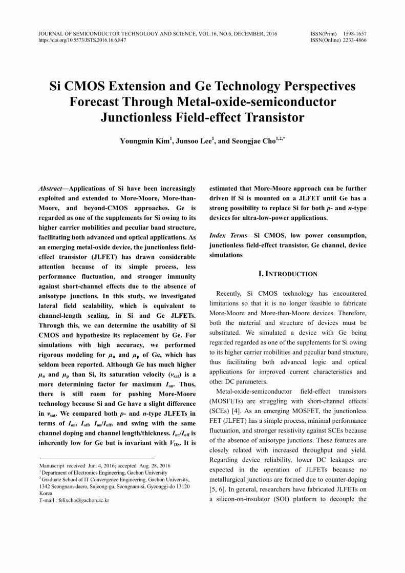
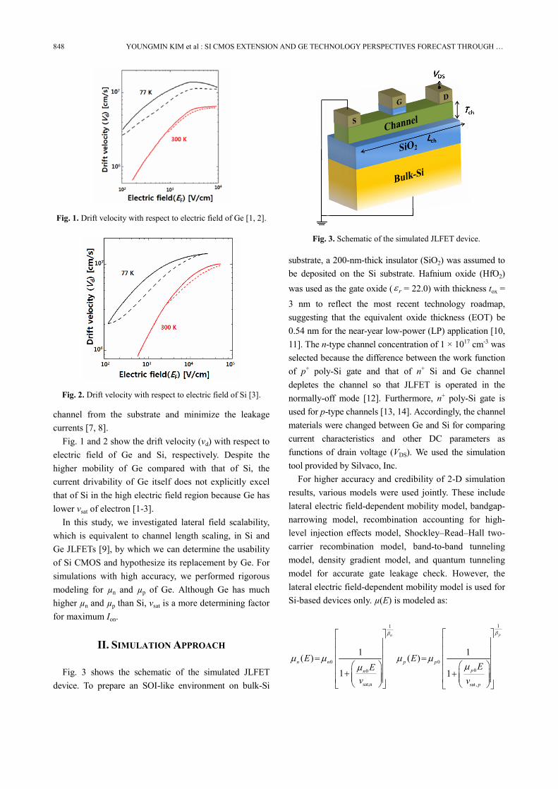
Fig. 1 and 2 show the drift velocity (vd) with respect to electric field of Ge and Si, respectively. Despite the higher mobility of Ge compared with that of Si, the current drivability of Ge itself does not explicitly excel that of Si in the high electric field region because Ge has lower vsat of electron [1-3].
In this study, we investigated lateral field scalability, which is equivalent to channel length scaling, in Si and Ge JLFETs [9], by which we can determine the usability of Si CMOS and hypothesize its replacement by Ge. For simulations with high accuracy, we performed rigorous modeling for µn and µp of Ge. Although Ge has much higher µn and µp than Si, vsat is a more determining factor for maximum Ion.
II. SIMULATION APPROACH
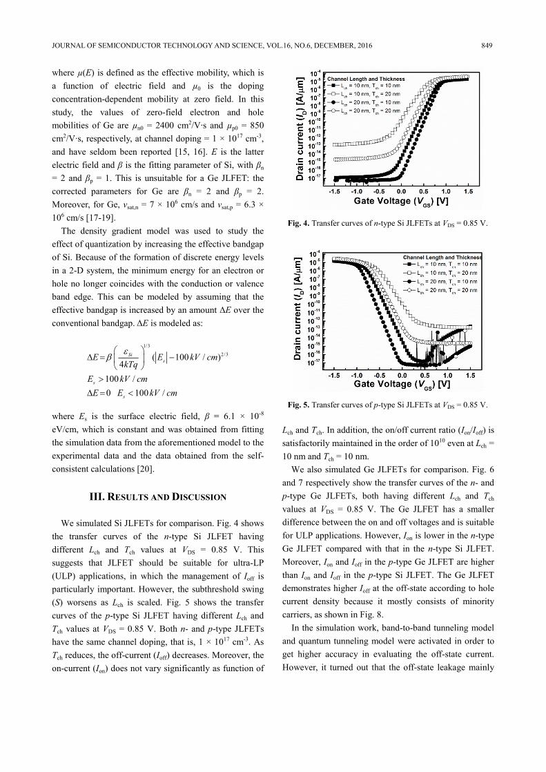
Fig. 3 shows the schematic of the simulated JLFET device. To prepare an SOI-like environment on bulk-Si
substrate, a 200-nm-thick insulator (SiO2) was assumed to be deposited on the Si substrate. Hafnium oxide (HfO2) was used as the gate oxide ( re = 22.0) with thickness tox = 3 nm to reflect the most recent technology roadmap, suggesting that the equivalent oxide thickness (EOT) be 0.54 nm for the near-year low-power (LP) application [10, 11]. The n-type channel concentration of 1 × 1017 cm-3 was selected because the difference between the work function of p+ poly-Si gate and that of n+ Si and Ge channel depletes the channel so that JLFET is operated in the normally-off mode [12]. Furthermore, n+ poly-Si gate is used for p-type channels [13, 14]. Accordingly, the channel materials were changed between Ge and Si for comparing current characteristics and other DC parameters as functions of drain voltage (VDS). We used the simulation tool provided by Silvaco, Inc.
For higher accuracy and credibility of 2-D simulation results, various models were used jointly. These include lateral electric field-dependent mobility model, bandgap-narrowing model, recombination accounting for high-level injection effects model, Shockley–Read–Hall two-carrier recombination model, band-to-band tunneling model, density gradient model, and quantum tunneling model for accurate gate leakage check. However, the lateral electric field-dependent mobility model is used for Si-based devices only. µ(E) is modeled as:
1
0
0
sat,n
1( )1
n
n n
n
EE
v
b
m mm
é ùê úê ú= ê úæ öê ú+ ç ÷ç ÷ê úè øë û
1
0
0
sat ,
1( )
1
p
p pp
p
EE
v
b
m mm
é ùê úê ú
= ê úæ öê ú+ ç ÷ç ÷ê úè øë û
Fig. 1. Drift velocity with respect to electric field of Ge [1, 2].
Fig. 2. Drift velocity with respect to electric field of Si [3].
Fig. 3. Schematic of the simulated JLFET device.
JOURNAL OF SEMICONDUCTOR TECHNOLOGY AND SCIENCE, VOL.16, NO.6, DECEMBER, 2016 849
where µ(E) is defined as the effective mobility, which is a function of electric field and µ0 is the doping concentration-dependent mobility at zero field. In this study, the values of zero-field electron and hole mobilities of Ge are µn0 = 2400 cm2/V·s and µp0 = 850 cm2/V·s, respectively, at channel doping = 1 × 1017 cm-3, and have seldom been reported [15, 16]. E is the latter electric field and β is the fitting parameter of Si, with βn = 2 and βp = 1. This is unsuitable for a Ge JLFET: the corrected parameters for Ge are βn = 2 and βp = 2. Moreover, for Ge, vsat,n = 7 × 106 cm/s and vsat,p = 6.3 × 106 cm/s [17-19].
The density gradient model was used to study the effect of quantization by increasing the effective bandgap of Si. Because of the formation of discrete energy levels in a 2-D system, the minimum energy for an electron or hole no longer coincides with the conduction or valence band edge. This can be modeled by assuming that the effective bandgap is increased by an amount ΔE over the conventional bandgap. ΔE is modeled as:
1/3
2/3( 100 / )4
100 /0 100 /
Sis
s
s
E E kV cmkTq
E kV cmE E kV cm
ebæ ö
D = -ç ÷è ø
>D = <
where Es is the surface electric field, β = 6.1 × 10⁻⁸ eV/cm, which is constant and was obtained from fitting the simulation data from the aforementioned model to the experimental data and the data obtained from the self-consistent calculations [20].
III. RESULTS AND DISCUSSION
We simulated Si JLFETs for comparison. Fig. 4 shows the transfer curves of the n-type Si JLFET having different Lch and Tch values at VDS = 0.85 V. This suggests that JLFET should be suitable for ultra-LP (ULP) applications, in which the management of Ioff is particularly important. However, the subthreshold swing (S) worsens as Lch is scaled. Fig. 5 shows the transfer curves of the p-type Si JLFET having different Lch and Tch values at VDS = 0.85 V. Both n- and p-type JLFETs have the same channel doping, that is, 1 × 1017 cm-3. As Tch reduces, the off-current (Ioff) decreases. Moreover, the on-current (Ion) does not vary significantly as function of
Lch and Tch. In addition, the on/off current ratio (Ion/Ioff) is satisfactorily maintained in the order of 1010 even at Lch = 10 nm and Tch = 10 nm.
We also simulated Ge JLFETs for comparison. Fig. 6 and 7 respectively show the transfer curves of the n- and p-type Ge JLFETs, both having different Lch and Tch values at VDS = 0.85 V. The Ge JLFET has a smaller difference between the on and off voltages and is suitable for ULP applications. However, Ion is lower in the n-type Ge JLFET compared with that in the n-type Si JLFET. Moreover, Ion and Ioff in the p-type Ge JLFET are higher than Ion and Ioff in the p-type Si JLFET. The Ge JLFET demonstrates higher Ioff at the off-state according to hole current density because it mostly consists of minority carriers, as shown in Fig. 8.
In the simulation work, band-to-band tunneling model and quantum tunneling model were activated in order to get higher accuracy in evaluating the off-state current. However, it turned out that the off-state leakage mainly
Fig. 4. Transfer curves of n-type Si JLFETs at VDS = 0.85 V.
Fig. 5. Transfer curves of p-type Si JLFETs at VDS = 0.85 V.
850 YOUNGMIN KIM et al : SI CMOS EXTENSION AND GE TECHNOLOGY PERSPECTIVES FORECAST THROUGH …
comes from the drift and diffusion of minority carriers by switching on and off the tunneling models. No significant difference is found in case of n-type JLFETs. On the other hand, hole tunneling is clearly observed in case of p-type Si JLFET when the model is turned on. The tunneling current in the Ge device is not clearly distinguished since the tunneling component is buried in the drift-diffusion current of minority carriers. Thus, it can be judged that Ge JLFET is not superior in terms of off-state current due to its smaller energy bandgap, higher intrinsic carrier concentration, and higher minority carrier concentration, which leads to the higher off-state current by drift-diffusion of minority carriers. This is not as threatening as the leakage current by band-to-band tunneling in the off-state of the conventional MOSFET devices having anisotype junctions but surely needs to be controlled by more precisely prepared set of processing conditions.
Fig. 9 compares Ion and Ioff of Si and Ge JLFETs as functions of VDS. The Ion and Ioff values were extracted not from fixed VGS locations but from moving VGS points, depending on device conditions for fair comparisons. This is because the gate work function is not tuned device-wisely for obtaining the same Vth; thus, Vth values from different JLFETs were not adjusted to a fixed value. Further, Ion and Ioff were not measured at a set of fixed VGS values, instead have been read at VGS = Vth + 0.5 V and VGS = Vth - 0.7 V, respectively. Vth was extracted by the constant-current method at the reference current ID = 10-6 A/μm. The n-type Si JLFET shows higher Ion for VDS values than the Ge device because of its higher vsat for electron (107 cm/s versus 6.3 × 106 cm/s). In contrast, the n-type Ge JLFET demonstrates higher Ion with VDS < 0.2
Fig. 6. Transfer curves of n-type Ge JLFETs at VDS = 0.85 V.
Fig. 7. Transfer curves of p-type Ge JLFETs at VDS = 0.85 V.
Fig. 8. Hole current density of n-type (a) Ge, (b) Si JLFETs in the off-states.
Fig. 9. On-state currents of p-type (upper) and n-type (lower) Ge and Si JLFETs as a function of VDS.
JOURNAL OF SEMICONDUCTOR TECHNOLOGY AND SCIENCE, VOL.16, NO.6, DECEMBER, 2016 851
V by using a higher µn. For p-type junctionless FET, Ge device is superior to
Si one in terms of Ion over the entire VDS below 0.85 V. On the other hand, for n-type junctionless FET, Si device shows higher current drivability over most of the considered VDS region than Ge one due to its higher saturation velocity of electron in spite of smaller electron mobility compared with Ge. However, Ion cross-over takes place at VDS = 0.2 V. The absolute value of Ion drastically decreases below VDS = 0.2 V, the Ge JLFET shows higher Ion than Si device. At this cross-over point, the higher electron mobility of Ge defeats the lower saturation velocity of electron in Ge, and the higher low-field electron velocity of Ge becomes the dominant factor in determining the Ion. The allowable current drivability needs to be further discussed in various aspects but it is revealed that Ge JLFET becomes more suitable for sub-0.5-V low-voltage operation than Si device.
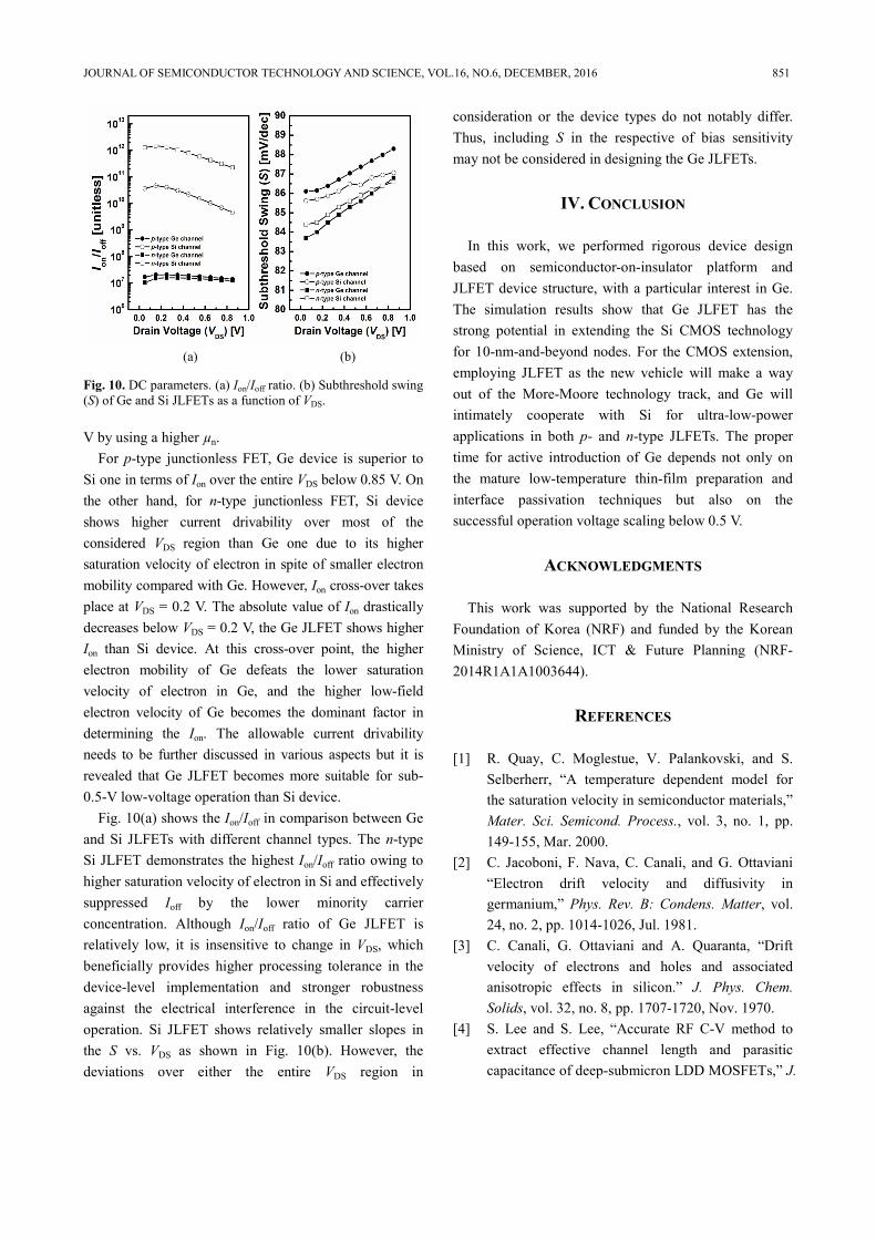
Fig. 10(a) shows the Ion/Ioff in comparison between Ge and Si JLFETs with different channel types. The n-type Si JLFET demonstrates the highest Ion/Ioff ratio owing to higher saturation velocity of electron in Si and effectively suppressed Ioff by the lower minority carrier concentration. Although Ion/Ioff ratio of Ge JLFET is relatively low, it is insensitive to change in VDS, which beneficially provides higher processing tolerance in the device-level implementation and stronger robustness against the electrical interference in the circuit-level operation. Si JLFET shows relatively smaller slopes in the S vs. VDS as shown in Fig. 10(b). However, the deviations over either the entire VDS region in
consideration or the device types do not notably differ. Thus, including S in the respective of bias sensitivity may not be considered in designing the Ge JLFETs.
IV. CONCLUSION
In this work, we performed rigorous device design based on semiconductor-on-insulator platform and JLFET device structure, with a particular interest in Ge. The simulation results show that Ge JLFET has the strong potential in extending the Si CMOS technology for 10-nm-and-beyond nodes. For the CMOS extension, employing JLFET as the new vehicle will make a way out of the More-Moore technology track, and Ge will intimately cooperate with Si for ultra-low-power applications in both p- and n-type JLFETs. The proper time for active introduction of Ge depends not only on the mature low-temperature thin-film preparation and interface passivation techniques but also on the successful operation voltage scaling below 0.5 V.
ACKNOWLEDGMENTS
This work was supported by the National Research Foundation of Korea (NRF) and funded by the Korean Ministry of Science, ICT & Future Planning (NRF-2014R1A1A1003644).
REFERENCES
[1] R. Quay, C. Moglestue, V. Palankovski, and S. Selberherr, “A temperature dependent model for the saturation velocity in semiconductor materials,” Mater. Sci. Semicond. Process., vol. 3, no. 1, pp. 149-155, Mar. 2000.
[2] C. Jacoboni, F. Nava, C. Canali, and G. Ottaviani “Electron drift velocity and diffusivity in germanium,” Phys. Rev. B: Condens. Matter, vol. 24, no. 2, pp. 1014-1026, Jul. 1981.
[3] C. Canali, G. Ottaviani and A. Quaranta, “Drift velocity of electrons and holes and associated anisotropic effects in silicon.” J. Phys. Chem. Solids, vol. 32, no. 8, pp. 1707-1720, Nov. 1970.
[4] S. Lee and S. Lee, “Accurate RF C-V method to extract effective channel length and parasitic capacitance of deep-submicron LDD MOSFETs,” J.
(a) (b)
Fig. 10. DC parameters. (a) Ion/Ioff ratio. (b) Subthreshold swing (S) of Ge and Si JLFETs as a function of VDS.
852 YOUNGMIN KIM et al : SI CMOS EXTENSION AND GE TECHNOLOGY PERSPECTIVES FORECAST THROUGH …
Semicond. Technol. Sci., vol. 15, no. 6, pp. 653-657, Dec. 2015.
[5] S. Kim, J. Seo, Y. Yoon, G. Yoo, Y. Kim, H. Eun, H. Kang, J. Kim, S. Cho, J. Lee, and I. Kang, “Design and Analysis of Sub-10 nm Junctionless Fin-Shaped Field-Effect Transistors,” J. Semicond. Technol. Sci., vol. 14, no. 5, pp. 508-517, Oct. 2014.
[6] F. Jazaeri, L. Barbut, A. Koukab, and J. Sallese, “Analytical model for ultra-thin body junctionless symmetric double gate MOSFETs in subthreshold regime,” Solid-State Electron., vol. 82, pp. 103-110, Apr. 2013.
[7] G. K. Celler and S. Cristoloveanu, “Frontiers of silicon-on-insulator,” J. Appl. Phys., vol. 93, no. 9, pp. 4955-4978, May 2013.
[8] J. Feng, Y. Liu, P. B. Griffin, and J. D. Plummer, “Integration of germanium-on-insulator and silicon MOSFETs on a silicon substrate,” IEEE Trans. Electron Devices, vol. 27, no. 11, pp. 911-913, Nov. 2006.
[9] C. Sun, R. Liang, L. Liu, J. Wang, and J. Xu, “Effect of channel doping profiles on performance of germanium-on-insulator based junctionless transistors.” Proc. 2015 IEEE International Sympo- sium on Next-Generation Electronics (ISNE), Taipei, Taiwan, May 4-6, 2015, pp. 1-3.
[10] International Technology Roadmap for Semicon- ductors (ITRS), 2013 Edition, Online available at http://www.itrs2.net.
[11] S. Lee, H. Kim, J. Lee, I. Yu, J. Lee and C. Hwang, “Effects of O3 and H2O as oxygen sources on the atomic layer deposition of HfO2 gate dielectrics at different deposition temperatures,” J. Mater. Chem. C, vol. 24, no. 2, pp. 2558-2568, Jan. 2014.
[12] J. P. Colinge, C. W. Lee, N. Dehdashti, R. Yan, I. Ferain, P. Razavi, A. Kranti, and R. Yu, Junctiobnless Transistors: Physics and Properties, Springer-Verlag, Berlin, Germany, 2011.
[13] C. W. Lee, F. Isabelle, A. Aryan, Y. Ran, D. Nima, R. Pedram, and J. P. Colinge, ”Performance estimation of junctionless multigate transistors,” Solid-State Electron., vol. 54, no.2, pp. 97-103, Feb. 2010.
[14] J. P. Colinge, C. W. Lee, A. Afzalian, N. Dehdashti, R. Yan, I. Ferain, P. Razavi, B. O’Neill, A. Blake, M. White, A. Kelleher, B. McCarthy, and R. Murphy, “SOI gated resistor: CMOS without junctions,” Proc. 2009 IEEE International SOI Conference, Foster City, USA, Oct. 5-8, 2009, pp. 1-2.
[15] S. M. Sze and J. C. Irvin, “Resistivity, mobility and impurity levels in GaAs, Ge, and Si at 300°K,” Solid State Electron., vol. 11, no. 6, pp. 599-602, Jan. 1968.
[16] P. P. Debye and E. M. Conwell, “Electrical properties of n-type germanium,” Phys. Rev. Appl, vol. 93, no. 4, pp. 693-706, Feb. 1954.
[17] D. M. Caughey and R. E. Thomas, “Carrier mobilities in silicon empirically related to doping and field,” Proc. IEEE, vol. 55, no. 12, pp. 2192-2193, Sep. 1967.
[18] G. Hellings, G. Eneman, R. Krom, B. D. Jaeger, J. Mitard, A. D. Keersgieter, T. Hoffmann, M. Meuris, and K. D. Meyer, “Electrical TCAD simulations of a Germanium pMOSFET technology,” IEEE Trans. Electron Devices, vol. 57, no. 10, pp. 2539-2546, Oct. 2010.
[19] L. Reggiani, C. Canali, F. Nava, and G. Ottaviani, “Hole drift velocity in germanium,” Phys. Rev. B: Condens. Matter, vol. 16, no. 6, pp. 2781-2791, Sep. 1977.
[20] S. A. Hareland, S. Jallepalli, G. Chindalore, W. K. Shih, A. F. Tasch, Jr., and C. M. Maziar, “A Simple Model for Quantum Mechanical Effects in Hole Inverson Layers in Silicon PMOS Device,” IEEE Transactions On Electron Devices,” vol. 44, no. 7, pp. 1172-1173, Jul. 1997.
Youngmin Kim received the B.S. degree from the Department of Electronics Engineering, Gachon University, Seongnam, Korea, in Feb. 2016, where he is currently pursuing the M.S. degree. His research interests include emerging memory
devices, nanoscale CMOS devices, and fabrication technology. He is a Student Member of the Institute of Electronics and Information Engineering (IEIE).
Junsoo Lee received the B.S. degree from the Department of Electronics Engineer, Gachon University, Seong- nam, Korea, in Feb. 2016, where he is currently pursuing the M.S. degree. His research interests include advanced CMOS devices such as tunneling
field-effect transistor (TFET), junctionless FET, and sharp-switching devices, and fabrication technology. He is a Student Member of IEIE.
JOURNAL OF SEMICONDUCTOR TECHNOLOGY AND SCIENCE, VOL.16, NO.6, DECEMBER, 2016 853
Seongjae Cho received the B.S. and the Ph.D. degrees in electrical engineering from Seoul National University, Seoul, Korea, in 2004 and 2010, respectively. He worked as an exchange researcher at the National Institute of Advanced
Science and Technology (AIST) in Tsukuba, Japan, in 2009. Also, he worked as a postdoctoral researcher at Seoul National University in 2010 and at Stanford University, CA, USA, from 2010 to 2013. Currently, he is an Assistant Professor at the Department of Electronics Engineering, Gachon University, Seongnam, Korea. His research interests include emerging memory technologies, nanoscale CMOS devices, optical devices, Si and group-IV-driven optical interconnect, and electrical-optical integrated circuits. He is a Life Member of IEIE and a Member of IEEE Electron Devices Society (EDS) and Photonics Society.