Embed Size (px)
Citation preview

ELECTRONICCASH REGISTER
MODEL ER-A320SRV Key : LKGIM7113RCZZPRINTER : CR-812A
(For "U" version)
CHAPTER 1. SPECIFICATIONS ....................................................................... 1
CHAPTER 2. OPTIONS ..................................................................................... 4
CHAPTER 3. SRV. RESET AND MASTER RESET.......................................... 5
CHAPTER 4. HARDWARE DESCRIPTION ...................................................... 5
CHAPTER 5. TEST FUNCTION ...................................................................... 10
CHAPTER 6. CIRCUIT DIAGRAM & PWB LAYOUT ...................................... 13
PARTS GUIDE
CONTENTS
Parts marked with " " are important for maintaining the safety of the set. Be sure to replace these parts with specifiedones for maintaining the safety and performance of the set.
SHARP CORPORATIONThis document has been published to be used for after sales service only.The contents are subject to change without notice.
SERVICE MANUAL

CHAPTER 1 . SPECIFICATIONS
1. Appearance/Rating
1) Appearance
2) Rating
Power source 120V AC m 10%, 60 Hz
Power consumption Stand-by: 9WOperating: 35W (Max.)
Operating temperature 32°F to 104°F (0°C to 40°C)
Operating humidity 10% to 90% (RH)
Physical dimensionsincluding the drawer
420 (W) x 423 (D) x 304 (H) mm(16.5 (W) x 16.7 (D) x 12.0 (H) in.)
Weight 13.0 kg (28.7 lbs.)
2. Keyboard
1) Standard keyboard layout
2) Key top name Standard key top
KEY TOP DESCRIPTION
RECEIPT Receipt paper feed key
JOURNAL Journal paper feed key
0~9, 00 Numeric keys
. Decimal point key
@/FOR Multiplication key
CL/C Clear key
PRINT Validation print key
Dept.1/+ Department 1/Plus key (Calc. mode)
Dept.2/– Department 2/Minus key (Calc. mode)
Dept.3/u Department 3/Multiplication key (Calc. mode)
Dept.4/v Department 4/Division key (Calc. mode)
Dept.5~10 Department 5~10 keys
PLU/SUB PLU/Subdepartment key
RCPT Receipt print key
- Discount key
AUTO Automatic sequencing key
% Percent key
NS No-sale key
Journal paper
Printer cover
Receipt paper
Drawer lock
Drawer
Customer display (Pop-up type)
Operator display
Mode switch
Keyboard
RCPT PRINT
PO %
CL
@FOR
RFND
VOID
987
654
321
0 00 •
CReceipt Journal
+
-
X
1
3
5 10
9
8
7
6
PLU/SUB NS TAX1SHIFT AUTO
CH CONV
MDSESBTL CHK
#/TM/SBTL
CA/AT
=
RA
CAL
RM
4
2

KEY TOP DESCRIPTION
RA/RM Received on account/Recall memory key (Calc. mode)
PO/CAL Paid out/Calculation mode key
RFND Refund key
VOID Void key
CH Charge key
CHK Check key
CONV Conversion key
MDSE SBTL Merchandise subtotal key
#/TM/SBTL Non-add code/Time display/Subtotal key
CA/AT/= Cash/Amount tendered/Equals key (Calc. mode)
TAX1 SHIFT TAX1 shift key
Optional key top
KEY TOP DESCRIPTION
Dept. 11~40 Department 11~40 keys
DEPT# Department number entry key
TAX2 SHIFT~TAX4SHIFT
Tax2~Tax4 shift keys
AUTO2 Automatic sequencing 2 key
CONV2~4 Conversion 2~4 keys
CA2 Cash total 2 key
CH2 Charge 2 key
- 2 Discount 2 key
%2 Percent 2 key
3. Display
1) Operator display
DISPLAY DEVICE LED
NUMBER OF LINE 1 line
NUMBER OF POSITIONS 10 positions
COLOR OF DISPLAY Green
CHARACTER SIZE 14.2mm (H) x 8.0mm (H)
2) Customer display (Pop-up type)
DISPLAY DEVICE LED
NUMBER OF LINE 1 line
NUMBER OF POSITIONS 7 positions
COLOR OF DISPLAY Green
CHARACTER SIZE 14.2mm (H) x 8.0mm (H)
3) Lamps
DESCRIPTION
AMOUNT 1~8
MINUS SIGN 2~10 : Floating
ERROR 10
PGM MODE 10
CA/ATCHCHK
10 : Lights up when a registrationis finalized by depressingCA/AT, CH or CHK key
SUBTOTAL/SHORT TENDER
10
CHANGE 10 : Lights up whenever thechange due amount appearsin the display.
DEPARTMENT 9~10 No zero-suppressed.
PLU 8~10 No zero-suppressed.
REPEAT 8 Endless count, starting from 2.
DECIMAL POINT 5~1 TAB (4~2)
RECEIPT OFF 9 —
VALIDATION 10 : Light up when the validationprinting is compulsory.
CONVERSION orCALC. MODE
10
DEPT REPEAT
PLU/SUB
RCPTOFF
: This appears when a transaction is finalized.
: This appears when the cash register computes the subtotal.
: This appears when the change due amount is displayed.
: This appears when for the calculator mode.
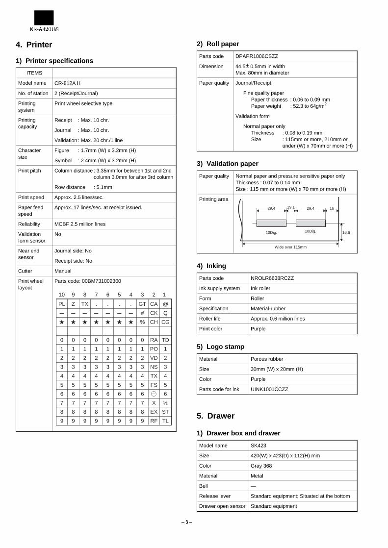
4. Printer
1) Printer specifications
ITEMS
Model name CR-812A
No. of station 2 (Receipt/Journal)
Printingsystem
Print wheel selective type
Printingcapacity
Receipt : Max. 10 chr.
Journal : Max. 10 chr.
Validation : Max. 20 chr./1 line
Charactersize
Figure : 1.7mm (W) x 3.2mm (H)
Symbol : 2.4mm (W) x 3.2mm (H)
Print pitch Column distance : 3.35mm for between 1st and 2nd column 3.0mm for after 3rd column
Row distance : 5.1mm
Print speed Approx. 2.5 lines/sec.
Paper feedspeed
Approx. 17 lines/sec. at receipt issued.
Reliability MCBF 2.5 million lines
Validationform sensor
No
Near endsensor
Journal side: No
Receipt side: No
Cutter Manual
Print wheellayout
Parts code: 00BM731002300
2) Roll paper
Parts code DPAPR1006CSZZ
Dimension 44.5m 0.5mm in widthMax. 80mm in diameter
Paper quality Journal/Receipt
Fine quality paperPaper thickness : 0.06 to 0.09 mmPaper weight : 52.3 to 64g/m2
Validation form
Normal paper onlyThickness : 0.08 to 0.19 mmSize : 115mm or more, 210mm or
under (W) x 70mm or more (H)
3) Validation paper
Paper quality Normal paper and pressure sensitive paper onlyThickness : 0.07 to 0.14 mmSize : 115 mm or more (W) x 70 mm or more (H)
Printing area
4) Inking
Parts code NROLR6638RCZZ
Ink supply system Ink roller
Form Roller
Specification Material-rubber
Roller life Approx. 0.6 million lines
Print color Purple
5) Logo stamp
Material Porous rubber
Size 30mm (W) x 20mm (H)
Color Purple
Parts code for ink UINK1001CCZZ
5. Drawer
1) Drawer box and drawer
Model name SK423
Size 420(W) x 423(D) x 112(H) mm
Color Gray 368
Material Metal
Bell —
Release lever Standard equipment; Situated at the bottom
Drawer open sensor Standard equipment
PL
-
0
1
2
3
4
5
6
7
8
9
½
@Z
-
0
1
2
3
4
5
6
7
8
9
TX
-
0
1
2
3
4
5
6
7
8
9
.
-
0
1
2
3
4
5
6
7
8
9
.
-
0
1
2
3
4
5
6
7
8
9
.
-
0
1
2
3
4
5
6
7
8
9
.
-
0
1
2
3
4
5
6
7
8
9
GT
0
1
2
3
4
5
6
7
8
9
CA
RA
PO
VD
NS
TX
FS
X
EX
RF
TD
1
2
3
4
5
6
ST
TL
Q
CG
CK
CH
#
%
10 19 8 7 6 5 4 3 2
19.1
16.6
29.4 29.4
10Dig.10Dig.
Wide over 115mm
16
2) Money case
Separation from the drawer Allowed
Separation of the coin compartments from themoney case
Disallowed
Bill separator —
Number of compartments 5B/5C
3) Lock
Location of the lock Front
Method of lockingand unlocking
Locking : lnsert the drawer lock key into thelock and turn it 90 degreescounterclockwise.
Unlocking : lnsert the drawer lock key into thelock and turn it 90 degreesclockwise.
Key No. SK1-1
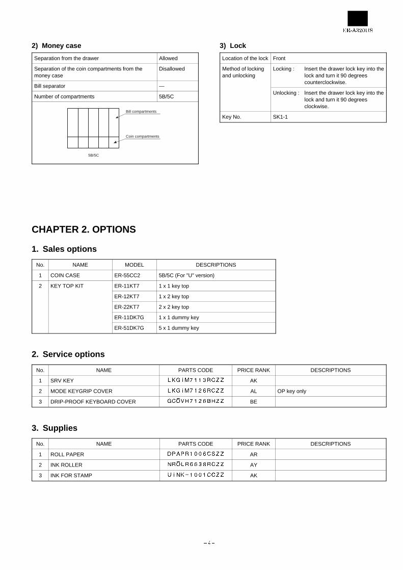
CHAPTER 2. OPTIONS
1. Sales options
No. NAME MODEL DESCRIPTIONS
1 COIN CASE ER-55CC2 5B/5C (For "U" version)
2 KEY TOP KIT ER-11KT7 1 x 1 key top
ER-12KT7 1 x 2 key top
ER-22KT7 2 x 2 key top
ER-11DK7G 1 x 1 dummy key
ER-51DK7G 5 x 1 dummy key
2. Service options
No. NAME PARTS CODE PRICE RANK DESCRIPTIONS
1 SRV KEY AK
2 MODE KEYGRIP COVER AL OP key only
3 DRIP-PROOF KEYBOARD COVER BE
3. Supplies
No. NAME PARTS CODE PRICE RANK DESCRIPTIONS
1 ROLL PAPER AR
2 INK ROLLER AY
3 INK FOR STAMP AK
5B/5C
Bill compartments
Coin compartments

CHAPTER 3. SRV RESET AND MASTER RESET
The SRV key is used for operating in the SRV mode.
1. SRV reset (Program Loop Reset)Used to return the machine back to its operational state after a lockuphas occurred.
Procedure· Method 1
1) Unplug the AC cord from the wall outlet.2) Set the mode switch to (SRV’) position.3) Plug in the AC cord to the wall outlet.4) Turn to (SRV) position from (SRV’) position.
· Method 2
1) Set the mode switch to PGM position.2) Unplug the AC cord from the wall outlet.3) While holding down JOURNAL FEED key and RECEIPT FEED
key, plug in the AC cord from the wall outlet.
Note: 1. The ER-A320 printer will cycle and print the following on thejournal
2. Master reset (All memory clear)Used to clear all memory contents and return machine back to initialsettings.(Returns keyboard back to the default keyboard layout.)
Procedure1) Unplug the AC cord from the wall outlet.
2) Set the MODE switch to the (SRV’) position.
3) Plug in the AC cord to the wall outlet.
4) While holding down JOURNAL FEED key, turn from (SRV’) posi-tion to the (SRV) position.
Note: 1. The ER-A320 display will flash the "." decimal point at theright most position and will beep 3 times.
2. The ER-A320 printer will cycle and print the following on thejournal
CHAPTER 4. HARDWARE DESCRIPTION
1. Block diagram
2
1
CPUµPD78045
S-RAM256 kbit
ADDRESSLATCH
PRINT WHEELMG DRIVER
STAMP, PAPERFEED DRIVER
MOTORDRIVER
PRINTER
CR-812A
SEGMENT DRIVER
DIGIT DRIVER
OP.DISPLAY
7SEG LED10DIG
POP-UPDISPLAY
7SEG LED7DIG
DRIVER
DRIVER DRAWER
BUZZER
KEYBOARD8X9 72KEY
MODESWITCH8SIGNAL
DC-DC CONVERTER
NI-MH BATTERY
VOLTAGEREGULATOR
TRANSFORMER
PRINTER POWER SOURCE : +18V
DISPLAY POWER SOURCE : +5.5V
ADDRESS BUS
HAMMER COMMON SIGNAL
LATCHSIGNAL
DIGIT SIGNAL
STROBESIGNAL
RETURNSIGNAL
ADDRESS BUS DATA BUS
DRIVE SIGNAL
DRIVE SIGNAL
DRIVE SIGNAL
TIMING SIGNAL
DRIVE SIGNAL
DRIVE SIGNAL
CHIP SELECTSIGNAL

2. CPU (UPD78045F) pin configuration
No.PIN
NAMESIGNALNAME
DESCRIPTION I/O
1 P94 DIG7 Display digit 7 O H
2 P93 DIG6 Dlsplay digit 6 O H
3 P92 DIG5 Display digit 5 O H
4 P91 DIG4 Display digit 4 O H
5 P90 DIG3 Display digit 3 O H
6 P81 DIG2 Display digit 2 O H
7 P80 DIG1 Display digit 1 O H
8 VDD VDD +5V
9 P27 AD7 RAM Address & Data bus 7Printer magnet 8
I/O H
10 P26 AD6 RAM Address & Data bus 6Printer magnet 7
I/O H
11 P25 AD5 RAM Address & Data bus 5Printer magnet 6
I/O H
12 P24 AD4 RAM Address & Data bus 4Printer magnet 5
I/O H
13 P23 AD3 RAM Address & Data bus 3Printer magnet 4
I/O H
14 P22 AD2 RAM Address & Data bus 2Printer magnet 3
I/O H
15 P21 AD1 RAM Address & Data bus 1Printer magnet 2
I/O H
16 P20 AD0 RAM Address & Data bus 0Printer magnet 1
I/O H
17 /RESET /RESET Reset signal I L
18 P74 NU NU O H
19 P73 NU NU O H
20 AVSS AVSS GND
21 P17 KR11 Key return signal 11 I H
22 P16 KR10 Key return signal 10 I H
23 P15 KR9 Key return signal 9 I H
24 P14 KR8 Key return signal 8 I H
25 P13 KR7 Key return signal 7 I H
26 P12 KR6 Key return signal 6 I H
27 P11 KR5 Key return signal 5 I H
28 P10 VB Battery voltage I
29 AVDD AVDD +5V
30 AVREF AVREF +5V (VCC)
31 XT1 P04 Sub clock: 32.768 kHz I
32 XT2 XT2 O
33 VSS VSS GND
34 X1 X1 Main clock: 4.19 MHz I
35 X2 X2 O
36 P37 MD Printer motor ON signal O H
37 P36 BUZ Buzzer ON signal O H/L
38 P35 RF Receipt paper feed signal O H
39 P34 JF Journal paper feed signal O H
40 P33 STAMP Stamp ON signal O H
41 P32 /ALE Address latch signal O
42 P31 /CE Chip select signal O L
No.PIN
NAMESIGNALNAME
DESCRIPTION I/O
43 P30 /WE Write signal O L
44 P03 RMS NU I
45 P02 JMS Drawer open sensor I
46 P01 a Printer timing signal I H
47 P00 PE Power enable signal I H
48 IC IC VSS
49 P72 P72 NU O H
50 P71 MG10 Printer magnet 10 O H
51 P70 MG9 Printer magnet 9 O H
52 VDD VDD +5V
53 P127 R-COM Printer receipt commonsignal
O H
54 P126 J-COM Printer journal commonsignal
O H
55 P125 VDD Mode signal (VDD) I H
56 P124 DR1 Standard drawer drive signal O H
57 P123 KR4 Key return signal 4 I H
58 P122 KR3 Key return signal 3 I H
59 P121 KR2 Key return signal 2 I H
60 P120 KR1 Key return signal 1 I H
61 P117 A14 RAM Address 14 O
62 P116 A13 RAM Address 13 O
63 P115 A12 RAM Address 12 O
64 P114 A11 RAM Address 11 O
65 P113 A10 RAM Address 10 O
66 P112 A9 RAM Address 9 O
67 P111 A8 RAM Address 8 O
68 P110 DR2 Option drawer drive signal O H
69 P107 DP/ST8 Display segment signal DPKey strobe signal 8
O H
70 P106 G/ST7 Display segment signal GKey strobe signal 7
O H
71 VLOAD VLOAD GND
72 P105 F/ST6 Display segment signal FKey strobe signal 6
O H
73 P104 E/ST5 Display segment signal EKey strobe signal 5
O H
74 P103 D/ST4 Display segment signal DKey strobe signal 4
O H
75 P102 C/ST3 Display segment signal CKey strobe signal 3
O H
76 P101 B/ST2 Display segment signal BKey strobe signal 2
O H
77 P100 A/ST1 Display segment signal AKey strobe signal 1
O H
78 P97 DIG10 Display digit signal 10 O H
79 P96 DIG9 Display digit signal 9 O H
80 P95 DIG8 Display digit signal 8 O H

3. RAM control
/WE: Write signalWhen the signal is low, writing is performed. When the sig-nal is high, reading is performed.
/CE: Chip select signal
A8-A14: Address bus
AD0-7: Address/Data bus
A0-1: Address bus signal
/ALE: Address latch signal
Address signals A0-A7 are used commonly with the data bus. Whenthe address latch signal /ALE is input to IC3, the address/data bussignal AD0-AD7 access the RAM as address signals A0-A7.
(READ)
As shown in the attached time chart, address signals are outputtedfrom P20-P27, P111-P117, and the lower address is latched with P32.The modes at P20-P27 are changed to the input mode. The chipenable signal (P31) is output for the RAM. Then the output data fromthe RAM are read from P20-P27.
(WRITE)
As shown in the attached time chart, address signals are output fromP20-P27, P111-P117, and the lower address is latched with P32. Thewrite enable signal (P30) is output. The write data to the RAM areoutput from P20-P27. Then the chip enable signal (P31) is output towrite the data.
5. Printer motor drive circuit
1) Printer motor drive and brake circuit
The printer motor is operated by switching operation of transistor Q17with the motor drive signal MD from the CPU.
IC2CPU
IC374HC373
IC14S-RAM
A8~A14
/ALEA0~A7
AD0~AD7
AD0~AD7
/WE
/CE
P111~P117
P20~P27
P32
P30
RAM /OE
P20~P27
P20~P27
RAM Data IN
RAM control
(WRITE cycle)
Upper address
Lower address Input data to RAM
15ns or above
15ns or above
30ns or above
0ns or aboveLower address latch signal
30ns or above
50ns or above
Fixed to LOW.
0ns or above
60ns or aboveREAD timing
Select
Input
Output
Hammer common
RAM /WE
RAM /CS
P20~P27
P111~P117
P20~P27
P32
P30
RAM /OE
P31
P20~P27
(READ cycle)
Upper address
Lower address RAM data output
15ns or above
15ns or above 70ns or above
0ns or aboveLower address latch signal
30ns or above
Fixed to HIGH.
Fixed to LOW
READ timing
SelectInput
Output
70ns or above
Hammer common
RAM control
RAM /WE
RAM /CS
P20~P27
IC2CPU
VP : +18VQ17
B1340
R78470
IC6BKID65003P
MD
R792.7K
R80
22K
C32220P
Q18B926
R812.7K
VM
M

2) Print solenoid drive circuit
Since the address bus is used to drive the print solenoid, an access tothe RAM cannot be performed during printing. The common voltage ofthe print solenoid is supplied by switching operations of transistorsQ20 and Q19 with the J-COM signal and the R-COM signal.
3) Paper feed solenoid and stamp solenoid drivecircuit
RF: Paper feed solenoid drive signal (Receipt side)
JF: Paper feed solenoid drive signal (Journal side)
STAMP: Stamp solenoid drive signal (Receipt side)
4) Timing signal circuit
The timing signal a is delivered to the CPU by the photo transistorattached to the printer.
5. Drawer drive circuit
The solenoid is driven by switching operation of transistor Q21 with thedrive signal DR1 from the CPU.
When an option drawer is used, the parts enclosed with the dotted linemust be attached to the PWB.
IC2CPU
AD0
AD2
AD4
AD6
AD7
VP : +18VQ19B926
R822.7KIC6D
KID65003PJ-COM
R83220/2W
VJ
D281N4002
AD1
AD3
AD5
MG10
MG9
IC7B
IC7C
IC7G
IC8B
IC8D
IC7E
IC7D
IC7F
IC8C
IC8A
JM2
JM1
JM3
JM4
JM5
JM6
JM7
JM8
JM9
JM10
VP : +24VQ20B926
R842.7KIC6C
KID65003PR-COM
R85220/2W
VR
D291N4002
AD0
AD2
AD4
AD6
AD7
AD1
AD3
AD5
MG10
MG9
IC8E
IC8F
IC9C
IC9E
IC9G
IC9A
IC8G
IC9B
IC9F
IC9D
RM2
RM1
RM3
RM4
RM5
RM6
RM7
RM8
RM9
RM10
R1361K
D30RB441Q
C40100µF/16V
+
R1371K
D31RB441Q
C41100µF/16V
+
IC2CPU
RF
JF
STAMP
1
1
76G
7A
6F
VM
IC2CPU
C371000P
50V
VCC:+5V
C2910U/16V
α
R1331K
IC2CPU
VP : +18V
R531K
R5415K
Q21C3784
DR1
VP : +18V
R891K
Q14C3784
DR2
JMS
R574.7K
R5515K
L2
STANDARD DRAWER
OPTION DRAWER

6. Keyboard circuit
The keyboard performs key scanning with the eight strobe signalsST1-ST8, and returns a signal on KR1-KR9 to the CPU.
The mode switch performs scanning with the eight strobe signals ST1-ST8, and returns the return signal KR10 to the CPU. When the modeswitch is at SRV position, the reset signal /RESET is outputted.
7. Display circuit
The 7-segment LED is used in the display. The operator display uses10 digit signals, and the pop-up display uses 7 digit signals.
8. Power supply circuit
9. Clock generator circuit
X2: 4.19MHz is inputted as the CPU main clock.
X1: 32.768KHz is inputted as the time renewal clock.
IC2CPU
ST8
ST6
ST4
ST2
ST1
ST7
ST5
ST3
KEY MATRIX
KR1
KR2
KR3
KR4
KR6
KR7
KR8
KR5
KR9
RA256K X 8
R10256K
D9
D11
D13
D15
D16
D10
D12
D14
MODE SWITCH
ST1~ST8
/RESET
KR10C11
M104
R4056K
D171SS133
DIG1'DIG9'DIG10' DIG2'
A,B,C,D,E,F,G,DP
DP' G' F' E' D' C' B' A'
A',B',C',D',E',F',G',DP' A',B',C',D',E',F',G',DP'
DIG1-DIG10
FND5 FND1FND4,3,2
IC2CPU
+6V
POP UPDISPLAY
DIG1'-7'
Operator Display
DP~A
REGULATORCIRCUIT
F1T1AL/250V
P-OFFCIRCUIT
REGULATOR
CIRCUIT
BATTERY
VP:+18V
+6v
VCC:+5VPE
VDD:+5V
: PRINTER, DRAWER
: DISPLAY
: CPU,RAMVB
POWERTRANSFOR
MER
CIRCUIT
IC2CPU
X132.768KHz
C1433P
C1622P
R51330K
R931M
X24.19MHz
X2
X1
XT2
P04

10. Buzzer circuit
This circuit sounds buzzer with the BUZ signal from the CPU.
11. Reset circuit
The reset signal is formed with VCC and VDD. The /RESET signal isalso outputted when the mode switch is at SRV position.
CHAPTER 5. TEST FUNCTION
1. Start of test functionThe following key operation is required in the SRV mode to start thetest.
XXXX ST
Test command
Master reset is required when the system is to be started for the firsttime.
2. List of test commands
No. Test contents Key operations
1 Mode switch test 1 ST
2 Keyboard test XXXX02 ST
3 Display and Buzzer test 3 ST
4 Standard Drawer test 4 ST
5 Option Drawer test 14 ST
6 Printer test 5 ST
7 RAM test 6 ST
NOTE-1: Test message is printed on the journal
NOTE-2: The contents of the totalizer and the preset values are noterased by the test.
3. Test function
1) Test No. 1: Mode switch testKey operation
1 ST
Then, turn the mode switches in the following order.
In the mode switch test, turn the switch rhythmically.
MODE: SRV PGM VOID OFF OP X/Z REGMGR X1/Z1 X2/Z2 SRV
DISPLAY: (1) (2) OFF (3) (4) (5) (6) (7) (0)
Description
As the mode switch position number is displayed, check the num-ber.
Termination
The test can be terminated when the mode switch is turned to theSRV side from other position.
Termination print at normal end
Termination print and error
IC2CPU
/RESET
VDD
VCC
D241SS133
C1822U/16V
+
+C1910U/50V
Q16C3198
R591K
MODE SWITCH
/RESET
C110.1µ
R581K
IC2CPU
/RESET
VDD
VCC
D241SS133
C1822U/16V
+
+C1910U/50V
Q16C3198
R591K
MODE SWITCH
/RESET
C11M104
R581K

2) Test No. 2: Keyboard testKey operation
X X X X 02 ST
Sum check data Test command
(1) Enter the test command in succession to the sum check dataof the model.
Model nameSum check data
(Standard keyboard data)
ER-A320 2518
NOTE: Sum check dataThe check sum is a decimal number obtained byconverting the hard code hexadecimal total of allkeys.The CA/AT key are the exception.
(2) Next, push every key on the keyboard except for the receiptand journal keys.When the CA/AT key is pressed, the termination printout isimmediately produced assuming that all keys have beenpressed.There is no order in which the keys have to be depressed.Display: 02 XX XX=position code.
[Keyboard position code of model vs. key to be pressed][All key position code]
[ER-A320 standard keyboard layout]
Description
Until the depression of the ST key, the sum of key position codesis compared with the sum check data, except for the CA/AT key.
Termination
The test terminates with the depression of the CA/AT key and the termination printout is produced.
Termination print at normal end
Termination print at error
3) Test No.3: Display and buzzer testKey operation
3 ST
Description
Continuous beeps and the display are tested.
The decimal point is shifted digit by digit from the lowest digit(every 200 msec).Then all segments are lighted (for about 1 sec).
Pressing any key will terminate the test.
Check items
Check that each position display is correct.Check that the display is even and uniform.Check that the buzzer sound is normal. (No interruption and vibra-tions of sounds.)
Test end
End print
4) Test No. 4: Drawer open testKey operation
4 ST : For standard drawer
Description
With this test, the drawer opens and its state is displayed in thefollowing manner:
Drawer open XX 0 XX=04
Drawer closed XX C
When the model that has no drawer sensor switch, displayed is"C".
Termination
With depression of any key
Termination print 04 (For standard drawer)
65 68 67 58 77 78
38
37
27
18
08
48
47
28
17
07
57
46
36
16
06
56
35
75
05
25
55
45
76
15
26
66
42
32
72
0212
62
52
22
R
70
10
00
J
41
21
11
61
31
20
01 14 04 03
24
44
64 63
34
74
53
33
73
13
54
43
23
67
56
35
75
05
25
70
10
00
41
21
11
31
20
01 04
63
34
74
13
54
43
23
03
53
33
73
68
55
45
76
15
26
78
38
37
27
08
77
48
4761
58
57
46
36
16
06
R J
1. 2. 3. 4. 5. 6. 7. 8. 9. 0.State of display
8. 8. 8. 8. 8. 8. 8. 8. 8. 8.State of display

5) Test No. 5: Continuous print testKey operation
5 ST
Description
The continuous printing as shown below is performed.
Termination
After pressing any key, one-cycle of printing is performed beforecompleting the operation.
Print format
6) Test No.6: RAM testKey operation
6 ST
Test content
The RAM of 256Kbit (standard provision) is checked.Read and write of each data are made to the addresses shown inthe table below to compare the data. If there is no error, the normalprint is made and the machine returns to the key wait state. If anerror occurs, the error print is made and the machine returns to thekey wait state.
[Test data]
Address 0000 0001 0002 0004 0008 0010 0020 0040
Data 00 01 02 04 08 10 20 40
Address 0080 0100 0200 0400 0800 1000 2000 4000
Data 80 EF FD FB F7 EF DF BF
Check item
Check the end print.
Test end
Normal end print
Error print
AAAA : Address No.
PL
-
0
1
2
3
4
5
6
7
8
9
½
@Z
-
0
1
2
3
4
5
6
7
8
9
TX
-
0
1
2
3
4
5
6
7
8
9
.
-
0
1
2
3
4
5
6
7
8
9
.
-
0
1
2
3
4
5
6
7
8
9
.
-
0
1
2
3
4
5
6
7
8
9
.
-
0
1
2
3
4
5
6
7
8
9
GT
0
1
2
3
4
5
6
7
8
9
CA
RA
PO
VD
NS
TX
FS
X
EX
RF
TD
1
2
3
4
5
6
ST
TL
Q
CG
CK
CH
#
%
0
1
2
3
4
5
6
7
EX
TL

87
65
43
21
ABCD
12
34
56
78
D C B A
1. P
OW
ER
VC
C
+6V
GN
D
VP
D6
1N40
02
4
1
2
3
BD
1
DI1
02
C4
330u
50v
UL
CS
A 2
.0A
/125
V
C2
6800
uF50
V
F1
Q1
2SC
4153
Q15
2SB
1243
HE
AT
SIN
K
R1
12K
ZD
1
MT
Z20
D
R2
3.9K
Q42
KT
C10
27
C1
M 0
.033
u
CN
1
PS
CN
CN
14/C
N14
-1
FM
CN
F2
UL
CS
A 4
.0A
/125
V
DIG
1~10
R12
112
K
+6V
R11
122
0
R12
2R
123
R12
4R
125
R11
2R
113
R11
4R
115
Q32
Q33
Q34
Q35
Q31
VC
C
PE
R4
2.7K
D3
1SS
133
56
12
34
IC1
KA
3406
3A
R5
100K
R3
56K
C5
3.3u
50V
C6
C 0
.1u
50V
C36
3300
P
R12
6R
127
R12
8R
129
R13
0
R11
6R
117
R11
8R
119
R12
0
ZD
2M
TZ
J18B
Q36
Q37
Q38
Q39
Q40
ST
1~S
T8
VB
C7
220P
Q2
KT
D14
14
R6
10
L1
220u
H
C8
1000
u16
V
ZD
5
MT
Z6.
2B
D7
1SS
133
C9
330u
16V
R7
3.6K
F
R8
1KF
CN
2
BT
CN
Q31
~Q
33: A
1271
R12
1~R
130:
12K
R11
1~R
120:
220
R10
11M
C34
0.1u
/50V
D4
PS
102R
R13
8
120
R9
100
BT
VD
D
GN
D
C10
330u
16V
CN
8
CN
9P
KE
Y72
ST
8
ST
1S
T2
ST
3S
T4
ST
5S
T6
ST
7
CN
5
CN
8P
R11
,13,
15,1
7,19
,21,
D15
1SS
133*
8
CN
7
23,2
5,27
,29
: 2.2
K
CN
15
PM
CN
PO
P U
P L
ED
CN
* 1
Q3~
Q12
:C31
98
Q34
~Q
40: B
926
D9
D10
D11
D12
D13
D14
D16
FN
D2
FN
D1
DIG
5'D
IG4'
DIG
3'D
IG2'
DIG
1'
R21
R23
R25
R27
R29
Q8
Q9
Q10
Q11
Q12
FN
D5
FN
D4
FN
D3
DIG
10'
DIG
9'D
IG8'
DIG
7'D
IG6'
R11
2.2K
R13
R15
R17
R19
Q4
Q5
Q6
Q7
Q3
SE
GA
~D
P
R38
2.2k
DP
R39
12k
1 1 6
F
5
1 0 7
G
5
1 2 5
E
5
MA
IN L
ED
PW
BE
'F
'G
'D
P'
R37 30
R36 30
R35 30
R34 30
C33
2200
P
Q13
C31
98
1 3 4
D
5
1 4 3
C
5
1 5 2
B
5
1 6 1
A
5
A'
B'
C'
D'
R33 30
R32 30
R31 30
R30 30
CA
122
00P
KR
1~K
R9
/RE
SE
TG
ND
ST
1~S
T8D
17
1SS
133
R40
56K
C11
C 0
.1u
50V
R13
2
12K
KR
10
RA
256
KX
8R
102
56K
IC5
KID
6500
3P
CH
AP
TE
R 6
. CIR
CU
IT D
IAG
RA
M &
PW
B L
AY
OU
T

87
65
43
21
ABCD
12
34
56
78
D C B A
2. C
PU
VM
VJ
R78
470
R79
2.7K
R80
22K
R81
2.7K Q
19
B92
6
R82 2.7K
D28
1N40
02
Q18
B92
6
C32
220P
15 2
6B12
56E
Q17
2SB
1340
VP
VP
VP
MD
R54
15K
CN
11
L2 B C
OR
E
R55
15K
JMS
CN
16
R89
1KD
R2
VP
Q21
C37
84
Q14
C37
84
C35
C 0
.1u
50V
KR
1~K
R11
A11
DIG
1~D
IG10
A 8A 9
A 1 0
R53
1K
RA
1
12K
*8
DR
1
D I G 8
A / S T 1
B / S T 2
DIG
7
C / S T 3
D / S T 4
E / S T 5
F / S T 6
G / S T 7
P 3 3
4 0
P94
1
P93
2
P92
3
P91
4
P90
5
P81
6
P80
7
VD
D 8
P27
9
P26
10
P25
11
P24
12
P23
13
P22
14
P21
15
P20
16
/RE
SE
T 1
7
P74
18
P73
19
AV
SS
20
P17
21
P16
22
P15
23
P14
24
P 1 3
2 5P 1 2
2 6P 1 1
2 7P 1 0
2 8A V D D
2 9A V R E F
3 0P 0 4
3 1X T 2
3 2V S S
3 3X 1
3 4X 2
3 5P 3 7
3 6P 3 6
3 7P 3 5
3 8P 3 4
3 9
P11
464
P11
563
P11
662
P11
761
P12
060
P12
159
P12
258
P12
357
P12
456
P12
555
P12
654
P12
753
VD
D52
P70
51
P71
50
P72
49
IC48
P00
47
P01
46
P02
45
P03
44
P30
43
P31
42
P32
41
P 9 5
8 0 P 9 6
7 9 P 9 7
7 8 P 1 0 0
7 7 P 1 0 1
7 6 P 1 0 2
7 5 P 1 0 3
7 4 P 1 0 4
7 3 P 1 0 5
7 2 V L O A D
7 1 P 1 0 6
7 0 P 1 0 7
6 9 P 1 1 0
6 8 P 1 1 1
6 7 P 1 1 2
6 6 P 1 1 3
6 5IC
2
UP
D78
045
D R 2
D P / S T 8R
87,8
8P
P:O
MP
:X
12k*
3
R13
4
D I G 9
D I G 1 0
VD
D
/RE
SE
TN
UN
U
DIG
6D
IG 5
DIG
4D
IG 3
DIG
2D
IG 1
AD
7A
D6
AD
5A
D4
AD
3A
D2
AD
1A
D0
KR
11K
R10
KR
9K
R8
aP
E
MG
10
MG
9
R-C
OM
J-C
OM
VC
C
RM
SJM
S
VD
D
NU
A12
A13
A14
KR
1K
R2
KR
3K
R4
/WE
/CE
/ALE
VC
C
DR
1
3
R76
R77
BZ
1
+
C13
10u
16V
C12
0.1u
12V
1
A
2B
VP
ST
AM
P
JF RF
/RE
SE
T
VD
D
J-C
OM
R-C
OM
R57
4.7K
(H)
3.3K
(L)
C18
22u
16V
D24
1SS
133
R59
1K
Q16
C31
98
R58
1K
U:X
11 6
6F10
76G
C42
22uF
/16V
C19
10uF
/10V
OS
D32
RB
441Q
VR
R83
220/
2W
Q20
B92
6
R84
2.7K
D29
1N40
02
R85
220/
2W
C40
100u
F/1
6V
C41
100u
F/1
6V
1 2 3 4 5 6 7 8 9 10 11 12 13 14 15 16 17 18 19 20 21 22 23 24 25 26 27 28 29 30
PR
CN
12
PR
CN
30P
13 4
6D
14 3
6C
16 1
7A
R13
6 1k
30 29 28 27 26 25 24 23 22 21 20 19 18 17 16 15 14 13 12 11 10 9 8 7 6 5 4 3 2 1
PR
CN
30P
PR
INT
ER
R13
7 1k
D30
RB
441Q
D31
RB
441Q
VJ
VR
VM
GN
D
15 2
7B
13 4
7D
11 6
7F
16 1
8A
14 3
8C
12 5
8E
10 7
8G
15 2
9B
13 4
9D
11 6
9F
R13
5
4.7K
C30
N.U
.
a
MG
9M
G 1
0
VD
D
AD
0A
D1
AD
2A
D3
AD
4A
D5
AD
6A
D7
AD
0A
D1
AD
2A
D3
AD
4A
D5
AD
6A
D7
A7
AD
7A
D6
A6
A5
AD
5A
D4
A4
/ALE
VC
C
C23
0.1u
12V
/OE
1
Q0
2
D0
3
D1
4
Q1
5
Q2
6
D2
7
D3
8
Q3
9
GN
D 1
0
VC
C20
Q7
19
D7
18
D6
17
Q6
16
Q5
15
D5
14
D4
13
Q4
12
/LE
11
IC3
74H
C37
3
C25
330P
R71
22KC24
1000
P
R13
31K
10 7
9G
12 5
9E
14 3
9C
16 1
9A
11 6
8F
13 4
8D
15 2
8B
10 7
7G
12 5
7E
14 3
7C
C37
1000
pF50
V
ST
AM
PJF R
F
/WE
MD
A0
AD
0A
D1
A1
A2
AD
2A
D3
A3
/ALE
X2
4.19
MH
zR93
1M
16 1
6A
VB
VD
D
K R 7
K R 6
K R 5
ST
1S
T2
B U Z
R50 33
0K
VC
C
R51
330K
X1
32.7
68K
Hz
C16
22P
C14
33P
D18
1SS
133*
4
KR
11
R13
1
12K
CN
9
1HC
KE
Y
D19
D20
A/S
T1~
DP
/ST
8 VP
ST
3S
T4
RM
S
R52
56K
IC6,
7,8,
9K
ID65
003P
U:X
V:O
C31
1000
P
R92
4.7K
TE
XT
1T
EX
T2
D21
/CE
A14
A12
A7
A6
A5
A4
A3
A2
A1
A0
AD
0A
D1
AD
2
VC
CCN
10
NE
CN
VC
C
U:X
V:X
TE
XT
3
VC
C
VD
D VD
D
A13
A8
A9
A11
A10
AD
7A
D6
AD
5A
D4
AD
3
/CE
C26
0.1u
12V
R68 22
K
C28
330P
C29
10u
16V
A14
1
A12
2
A7
3
A6
4
A5
5
A4
6
A3
7
A2
8
A1
9
A0
10
D0
11
D1
12
D2
13
GN
D14
VD
D28
/WE
27
A13
26
A8
25
A9
24
A11
23
/OE
22
A10
21
/CE
20
D7
19
D6
18
D5
17
D4
16
D3
15
IC4
S-R
AM
28P
C27
10u
16V
C39
10uF
/16V
|link
|pop
up.s
ch|p
ower
.sch

87
65
43
21
ABCD
12
34
56
78
D C B A
3. P
OP
-UP
DIS
PLA
Y
DIG
1'D
IG2'
DIG
3'D
IG4'
DIG
5'D
IG6'
DIG
7'
FN
D4
R10 27
R12 27
R14 27
FN
D3
FN
D2
FN
D1
R16 27
R18 27
R20 27
R22 27
R24 27
CN
1
PM
CN
PO
P U
P L
ED
CN
* 1
A'
B'
C'
D'
E'
F'
G'
DP
'

4. P
WB
LA
YO
T
M
AIN
PW
B L
AY
OU
T
PO
P-U
P P
WB
LA
YO
UT

CONTENTS
PARTS GUIDE
MODEL ER-A320SRV key : LKGiM7113RCZZPRINTER : CR-812AII
(For "U" & "A" Version)
1 Exteriors
2 Keyboard unit
3 Packing material & Accessories
4 Drawer box unit(SK-423type)
5 Main PWB unit
6 Pop up PWB unit
7 Articles for consumption
8 Service route options
■ Index
Because parts marked with "!" are indispensable for the machine safety maintenance and poeration, itmust be replaced with the parts specific to the product specification.
SHARP CORPORATIONThis document has been published to beused for after sales service only.The contents are subject to change withoutnotice.
ER-A320U/A
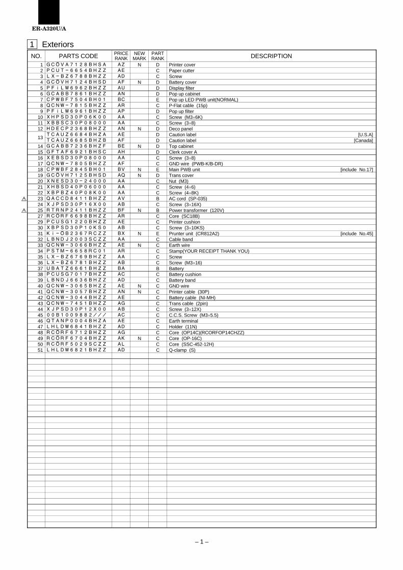
1 ExteriorsNO. PARTS CODE PRICE
RANKNEWMARK
PARTRANK DESCRIPTION
1 GCOVA7128BHSA AZ N D Printer cover 2 PCUT-6654BHZZ AE C Paper cutter 3 LX-BZ6788BHZZ AD C Screw 4 GCOVH7124BHSD AF N D Battery cover 5 PFILW6962BHZZ AU D Display filter 6 GCABB7861BHZZ AN D Pop up cabinet 7 CPWBF7504BH01 BC E Pop up LED PWB unit(NORMAL) 8 QCNW-7815BHZZ AR C P-Flat cable (15p)9 PFILW6961BHZZ AP D Pop up filter
10 XHPSD30P06K00 AA C Screw (M3´6K)11 XBBSC30P08000 AA C Screw (3´8)12 HDECP2368BHZZ AN N D Deco panel
13TCAUZ6684BHZA AE D Caution label [U.S.A]TCAUZ6685BHZB AF D Caution label [Canada]
14 GCABB7236BHZF BE N D Top cabinet 15 GFTAF6921BHSC AH D Clerk cover A 16 XEBSD30P08000 AA C Screw (3´8)17 QCNW-7805BHZZ AF C GND wire (PWB-K/B-DR)18 CPWBF2845BH01 BV N E Main PWB unit [include No.17]19 GCOVH7125BHSD AQ N D Trans cover 20 XNESD30-24000 AA C Nut (M3)21 XHBSD40P06000 AA C Screw (4´6)22 XBPBZ40P08K00 AA C Screw (4´8K)23! QACCD8411BHZZ AV B AC cord (SP-035)24 XJPSD30P16X00 AB C Screw (3´16X)25! RTRNP2411BHZZ BF N B Power transformer (120V)27 RCORF6698BHZZ AR C Core (SC18B)29 PCUSG1220BHZZ AE C Printer cushion 30 XBPSD30P10KS0 AB C Screw (3´10KS)31 KI-OB2367RCZZ BX N E Prunter unit (CR812A2) [include No.45]32 LBNDJ2003SCZZ AA C Cable band 33 QCNW-3066BHZZ AE N C Earth wire 34 PSTM-6658RC01 AR C Stamp(YOUR RECEIPT THANK YOU) 35 LX-BZ6769BHZZ AA C Screw 36 LX-BZ6781BHZZ AB C Screw (M3´16)37 UBATZ6661BHZZ BA B Battery 38 PCUSG7017BHZZ AC C Battery cushion 39 LBNDJ6636BHZZ AD C Battery band 40 QCNW-3065BHZZ AE N C GND wire 41 QCNW-3057BHZZ AN N C Printer cable (30P)42 QCNW-3044BHZZ AE C Battery cable (NI-MH)43 QCNW-7451BHZZ AG C Trans cable (2pin)44 XJPSD30P12X00 AB C Screw (3´12X)45 00B1009882/// AC C C.C.S. Screw (M3´5.5)46 QTANP0004BHZA AE C Earth terminal 47 LHLDW6841BHZZ AD C Holder (11N)48 RCORF6712BHZZ AG C Core (OP14C)(RCORFOP14CHZZ)49 RCORF6704BHZZ AK N C Core (OP-16C)50 RCORF5029SCZZ AL C Core (SSC-452-12H)51 LHLDW6821BHZZ AD C Q-clamp (S)
ER-A320U/A
– 1 –

1 Exteriors
RCP00301
1
2
3
4
5 67
8
9
11
10
12
13
14
15
16
18
362223
24
25
29
3031
33
34
35
32
16
16
17
42
16
16
16
1641
29
453035
30
29
43
44
27
46
47
3738
39
44
21
40
19
20
49
4832
51
50
ER-A320U/A
– 2 –

2 Keyboard unitNO. PARTS CODE PRICE
RANKNEWMARK
PARTRANK DESCRIPTION
1 LANGQ7604BHZZ AG C Mode sw angle 2 LKGIW0001BHZZ AS B Mode switch(Body) 3 QCNW-7804BHZZ AL C Mode cable 4 PHOG-1060CCZZ AA C Display cushion 5 XJPSD30P08000 AA C Screw (3´8)
6LKGIM7110BHZZ AE B MA key (MA)LKGIM7111BHZZ AE B OP key (OP)
7 JKNBZ6897BHZZ AG C Key cap (1´1)8 JKNBZ6896BHZA AG C Key top (1´1)9 JKNBZ6899BHZZ AH C Key cap (1´2)
10 JKNBZ6898BHZZ AH C Key top (1´2)
11
JKNBZ6905BHZZ AF C Key top (0)JKNBZ6908BHZZ AK C Key top (.)JKNBZ6911BHZZ AK C Key top (1)JKNBZ6912BHZZ AK C Key top (2)JKNBZ6913BHZZ AK C Key top (3)JKNBZ6914BHZZ AK C Key top (4)JKNBZ6915BHZZ AK C Key top (5)JKNBZ6916BHZZ AK C Key top (6)JKNBZ6917BHZZ AK C Key top (7)JKNBZ6918BHZZ AK C Key top (8)JKNBZ6919BHZZ AK C Key top (9)JKNBZ6920BHZZ AK C Key top (00)
12 JKNBZ6901BHZA AL C Key cap (2´2)13 JKNBZ6900BHZA AN C Key top (2´2)14 LFRM-6700BHZZ BB D Key frame 15 PGUMM6725BHZZ AZ C Key rubber 16 PSHEP6844BHZZ BC C Key sheet unit 17 LPLTM6705BHZZ AX C Key plate 18 XEBSD30P06000 AA C Screw (3´6)19 LHLDZ6837BHZZ AE C Holder L (YELLOW)20 LHLDZ6836BHZZ AE C Holder R (WHITE)
101 CLABH2516BHZZ AX N D Key label 501 DUNTK3986BHZZ BP N E Keyboard [include No.7~17,19,20,101]
3 Packing material & AccessoriesNO. PARTS CODE PRICE
RANKNEWMARK
PARTRANK DESCRIPTION
1 SPAKA8367BHZZ AT D Packing add L 2 PSHEP6681BHZZ AF C Packing sheet 3 SPAKA8366BHZZ AT D Packing add R 4 SPAKC3114BHZZ BB N D Packing case 5 SSAKH4231CCZZ AA D Vinyl bag (140´500mm)6 SSAKH3015CCZZ AA D Vinyl bag (260´360 30U)
7TINSE2400BHZZ AV N D Instruction book [U.S.A]TINSK2401BHZZ AZ N D Instruction book [Canada]
8 UINK-1001CCZZ AK S Ink for stamp (5cc)10 SSAKH3012CCZZ AA D Vinyl bag (80´120mm)11 LKGIM7331BHZZ AE B Lock key (1pc)
12LKGIM7110BHZZ AE B MA key (MA)LKGIM7111BHZZ AE B OP key (OP)
13TCADH6795BHZZ AC D Caution card (Red) [U.S.A]TCADH6788BHZA AC D Caution card (Black) [Canada]
14 UBNDA6630BHZZ AK C AC cord band 15 00BF703301010 AQ C Paper rolling shaft
ER-A320U/A
– 3 –

2 Keyboard unit
3 Packing material & Accessories
RCP00302
1
23
4
56 7
89
11
10
12
1314
15
16
17
1818
18
5
20
1920
19
20
19
18501
RCP00303
1
2
3
4
5
6
87
11
10
1213
15
14
ER-A320U/A
– 4 –

4 Drawer box unit(SK-423type)NO. PARTS CODE PRICE
RANKNEWMARK
PARTRANK DESCRIPTION
1CCABM7245BH03 BL N D Cabinet frame unit [U.S.A]CCABM7251BH04 BL N D Cabinet frame unit [Canada]
3 PGUMM6695BHZZ AE C Stopper gum 4 NROLP6650BHZZ AP C Roller 5 XUBSD30P08000 AA C Screw (3´8)6 LBRC-6666BHZZ AQ C Bracket (for 5B) [U.S.A]7 MSPRT6714BHZZ AE C Bill spring 8 MLEVF6695BHZZ AK C Bill lever 9 PSKR-6629BHZZ AL C Bill separator [Canada]
10 SSAKA5004CCZZ AA D Vinyl bag (100´300mm) [Canada]11 PSKR-6628BHZZ AG C Separator [Canada]12 GCAS-6682BHZZ AZ D Money case (5B/5C) [U.S.A]13 LX-BZ6776BHZZ AA C Screw 14 QSW-M6872BHZZ AR B Micro switch 15 CPLU-6647BH01 AY B Solenoid + Drawer cable 16 CFRM-6683BH01 AW E Lock frame unit 17 LX-BZ6775BHZZ AA C Screw (3´5)18 MSPRT6713BHZZ AD C Open lever spring 20 XRESJ50-06000 AA C E type ring (5mm)21 MCAMM6633BHZA AE C Lock cam 22 LFRM-6682BHZZ AN D Bell frame 23 XWSSD40-10000 AA C Washer 24 XNESD40-32000 AA C Nut (M4)25 PGUMM6696BHZZ AE C Gum leg 26 XHBSD30P12000 AA C Screw (3´12)27 MSPRC6712BHZZ AF C Push out spring 28 NROLP6650BHZZ AP C Roller 29 XNESD60-50000 AA C Nut (M6)30 XWSSD60-15000 AA C Washer (6mm)
31GDRW-6680BHZZ BE D Drawer case frame unit [U.S.A]GDRW-6678BHZZ BF D Drawer case frame unit [Canada]
32 GCOVA7146BHZZ AV D Front cover 33 LKGIW7330BHZZ AY B Lock key (body) 34 PRNGT6637BHZZ AA C Key ring 35 LKGIM7331BHZZ AE B Lock key (1pc)36 MSPRK6718BHZZ AF C Lock key spring
37LPLTM6674BH01 AX D Bottom plate [U.S.A]LPLTM6674BHZE AZ D Bottom plate [Canada]
38 SPAKA8255BHZZ AC D Paper pad 39 XHBSD40P12000 AA C Screw (4´12)40 MSPRB6711BHZZ AD C Earth spring 41 XHPSC30P08000 AA C Screw (3´8)42 DUNT-1306BHZA AX E Lock key unit 57 GCAS-6678BHZZ BC D Money case (4B/8C) [Canada]58 LBRC-6663BHZZ AQ C Bill bracket (for4B) [Canada]
501 CCAS-6682BH01 BF E Money case unit (5B/5C) [U.S.A]
502GDRW-6682BHZZ BH E Drawer case unit (for 5B/5C) [U.S.A]GDRW-6684BHZZ BH E Drawer case unit (for 4B/8C) [Canada]
503 CLOK-6676BH01 BH E Lock unit 504 CFRM-6682BH02 AQ E Bell frame unit (include No.22,26,27)505 CCAS-6678BH01 BF E Money case unit [Canada]
( U n i t )
901GBOXD7139BH01 BX N E Drawer box unit (SK-423 5B/5C) [U.S.A]GBOXD7144BH01 BY N E Drawer box unit (SK-423 4B/8C) [Canada]
ER-A320U/A
– 5 –

4 Drawer box unit(SK-423type)
RCP00304
3028
29
31
32
3334
35
25
3925
39
25
39
4041
28
2930
2120
37
36 42
502
38
38
24
2526
27
22
1314
1516
1718
23
9 10
57
85
505
5
5 558
7
11
501
55
56
12
5
7
8
5
1
for CANADA
for U.S.A.
504
503
3
15
ER-A320U/A
– 6 –

5 Main PWB unitNO. PARTS CODE PRICE
RANKNEWMARK
PARTRANK DESCRIPTION
1 LX-BZ6644RCZZ AA C Screw (3.5´8S)(LX-BZ6644BHZZ) [for HEAT SINK fixed]2 PRDAF6666BHZZ AN C Hheat sink [HEAT SINK]3 QCNCM1101BHZZ AC C Connector (5273-02A)(2P) [CN1]4 QCNCM7057BHZZ AB C Connector (5045-3)(3pin) [CN11]5 QCNCW2822BH3J AH N C Connector (PR)(MLX 52045-3045) [CN12]6 QCNCW6882BH1A AG C Connector (11P)(52011-1110)(ST TYPE) [CN7]7 QCNCW7081BHZZ AB C Connector (2P)(5267-02A)(Blue) [CN2]8 QCNCW7118BH0H AG C Connector (8P)(5229-08CPB) [CN5]9 QCNCW7118BH0I AG C Connector (K/B)(9P)(5229-09CPB) [CN8]
10 QCNCW7201BH1E AK C Connector (15P)(52806-1510) [CN15]11 QCNW-7805BHZZ AF C GND wire (PWB-K/B-DR)12 QCNW-7811BHZZ AM C F-LED cable (18P) [CN14,14-1]13 QCNW-7824BHZZ AE C GND wire 14! QFS-H0001QCZZ AG N A Fuse (UL/CSA 4.0A 125V 52SB) [F2]15! QFS-B0323QCZZ AC A Fuse (UL125V 2A) [F1]16 QFSHD2109AFZZ AC C Fuse holder (HD2109AF) [F1]17 RALMB6646BHZZ AQ B Buzzer [BZ1]18 RC-EZ106ARC1A AD C Capacitor (10WV 10mF) [C19]19 RC-KZ1054CCZZ AB C Capacitor (10WV 0.1mF) [C6,11,34,35]20 RC-Z1N104RCZZ AA C Capacitor (12WV 0.1mF)(RC-Z1N104BHZZ) [C12,23,26]21 RCILC6647RCZZ AE C Coil (220mH)(RCH-110)(RCILC6647BHZZ) [L1]22 RCRM-7001BHZZ AH B X-TAL (4.19MHz) [X2]23 RCRSP6676RCZZ AG B Crystal (DT38 32.768KHz) [X1]24 RMPTC8563QCJB AC B Block resistor (56KW´8 1/8W ±5%) [RA2]25 VCCCPU1HH220J AA C Capacitor (50WV 22PF)(VCCCPA1HH220J) [C16]26 VCCCPU1HH330J AB C Capacitor (50WV 33pF)(VCCCPA1HH330J) [C14]27 VCEAGA1CW106M AA C Capacitor (16WV 10mF) [C13,27,29,39]28 VCEAGA1CW107M AC C Capacitor (16WV 100mF) [C40,41]29 VCEAGA1CW226M AB C Capacitor (16WV 22mF) [C18,42]30 VCEAGA1CW337M AB C Capacitor (16WV 330mF) [C9,10]31 VCEAGA1HW335M AB C Capacitor (50WV 3.3mF) [C5]32 VCEAGD1CW108M AE C AL Capacitor (1000mF/16V) [C8]33 VCEAGD1HW337M AF C Capacitor (50WV 330mF) [C4]34 VCEAGU1HC688M AY N C Capacitor (50WV 6800mF) [C2]35 VCKYPU1HB102K AA C Capacitor (50WV 0.001mF)(VCKYPA1HB102K) [C24,31,37]36 VCKYPU1HB221K AB C Capacitor (50WV 220pF)(VCKYPA1HB221K) [C7,32]37 VCKYPU1HB331K AA C Capacitor (50WV 330pF)(VCKYPA1HB331K) [C25,28]38 VCKYPU1HB332K AA C Capacitor (50WV 3300pF)(VCKYPA1HB332K) [C36]39 VCQYNA1HM333K AA C Capacitor (50WV 0.033mF) [C1]40 VHD1N4002G/-1 AA B Diode (1N4002G) [D6,28,29]41 VHD1D4B42//-1 AD B Diode (1D4B42)(VHDDI102/BH-1) [BD1]42 VHDDSS133HV-1 AA B Diode (DSS133HV) [D3,7,9~17,24]43 VHDPS102R//-1 AD B Diode (PS102R) [D4]44 VHDRB441Q40-1 AD B Diode (RB441Q-40) [D30,31,32]45 VHEMTZ20D//-1 AA B Zener diode (MTZ20D) [ZD1]46 VHERD6.2EB/-1 AD B Zener diode (RD6.2EB)(VHEMTZ6.2B/-1) [ZD5]47 VHEMTZJ18B+-1 AC B Zener diode (MTZJ18B) [ZD2]48 VHID78045F097 AY N B CPU (D78045F097) [IC2]49 VHILH52B256N9 AW B IC (SRAM 256K 8´32K 100ns)(VHIG76C256F70) [IC4]50 VHIMC34063AM1 AG B IC (MC34063AM1)(VHIKA34063A-1) [IC1]51 VHIKID65003AP AE B IC (KD65003AP) [IC5~9]52 VHIMC74HC373N AK B IC (MC74HC373)(VHISN74HC373N) [IC3]53 VHPHDSP5621-1 AM B LED (2SEG)(HDSP5621) [FND1~5]
54VRD-RC2EY000J AA C Resistor (1/4W 0W ±5%) [R139,141]VRD-RC2EY000J AA C Resistor (1/4W 0W ±5%) [R140]
55 VRD-RC2EY100J AA C Resistor (1/4W 10W ±5%) [R6]56 VRD-RC2EY101J AA C Resistor (1/4W 100W ±5%) [R9]57 VRD-RC2EY102G AA C Resistor (1/4W 1KW ±2%)(VRD-RC2EY102F) [R8]58 VRD-RC2EY102J AA C Resistor (1/4W 1.0KW ±5%) [R53,58,59,76,77,133,136,137]59 VRD-RC2EY104J AA C Resistor (1/4W 100KW ±5%) [R5]60 VRD-RC2EY105J AA C Resistor (1/4W 1.0MW ±5%) [R93,101]61 VRD-RC2EY121J AA C Resistor (1/4W 120W ±5%) [R138]62 VRD-RC2EY123J AA C Resistor (1/4W 12KW ±5%) [R1,39,121~132]63 VRD-RC2EY153J AA C Resistor (1/4W 15KW ±5%) [R54,55]64 VRD-RC2EY221J AA C Resistor (1/4W 220W ±5%) [R111~120]65 VRD-RC2EY222J AA C Resistor (1/4W 2.2KW ±5%) [R11,13,15,17,19,21,23,25,27,29,38]66 VRD-RC2EY223J AA C Resistor (1/4W 22KW ±5%) [R68,71,80]67 VRD-RC2EY272J AA C Resistor (1/4W 2.7KW ±5%) [R4,79,81,82,84]68 VRD-RC2EY300J AA C Resistor (1/4W 30W ±5%) [R30~37]69 VRD-RC2EY334J AA C Resistor (1/4W 330KW ±5%) [R50,51]70 VRD-RC2EY362G AA C Resistor (1/4W 3.6KW ±2%)(VRD-RC2EY362F) [R7]71 VRD-RC2EY392J AA C Resistor (1/4W 3.9KW ±5%) [R2]72 VRD-RC2EY471J AA C Resistor (1/4W 470W ±5%) [R78]73 VRD-RC2EY472J AA C Resistor (1/4W 4.7KW ±5%) [R57,92,135]74 VRD-RC2EY563J AA C Resistor (1/4W 56KW ±5%) [R3,40,52,102]75 VRS-RE3DA221J AB C Resistor (2W 220W ±5%) [R83,85]76 VSKTA1271//-1 AE B Transistor (KTA1271)(VS2SA1271-/-1) [Q31,32,33]77 VS2SB1243++-1 AG N B Transistor (2SB1243) [Q15]78 VS2SB1340//-1 AL B Transistor (2SB1340) [Q17]79 VS2SB926-S/TC AD B Transistor (2SB926-S/TC)(KA1270)(VSKTA1270//-1) [Q18,19,20,34~40]
ER-A320U/A
– 7 –

5 Main PWB unitNO. PARTS CODE PRICE
RANKNEWMARK
PARTRANK DESCRIPTION
80 VSDSC001-//-1 AA B Transistor (2SC3198)(VS2SC3198-/-1) [Q3~13,16]81 VS2SC3784-/-1 AD B Transistor (2SC3784) [Q21]82 VS2SC4153-/-1 AG B Transistor (2SC4153) [Q1]83 VSKTC1027//-1 AG N B Transistor (KTC1027) [Q42]84 VSKTD1414//-1 AL B Transistor (KTD1414) [Q2]85 XBPSD30P06000 AA C Screw (3´6) [for TR fixed]
( U n i t )901 CPWBF2845BH01 BV N E Main PWB unit
6 Pop up PWB unitNO. PARTS CODE PRICE
RANKNEWMARK
PARTRANK DESCRIPTION
1 QCNCW7202BH1E AK C Connector (52807-1510) [CN1]2 VHPHDSP5621-1 AM B LED (2SEG)(HDSP5621) [FND1,2,3,4]3 VRD-RC2EY270J AA C Resistor (1/4W 27W ±5%) [R10,12,14,16,18,20,22,24]
901 CPWBF7504BH01 BC E Pop up PWB unit (NORMAL)
7 Articles for consumptionNO. PARTS CODE PRICE
RANKNEWMARK
PARTRANK DESCRIPTION
1 DPAPR1006CSZZ AR S Roll paper (5roll/pack)2 NROLR6638RCZZ AY S Ink roller (purple)3 UINK-1001CCZZ AK S Ink for stamp (5cc)
8 Service route optionsNO. PARTS CODE PRICE
RANKNEWMARK
PARTRANK DESCRIPTION
1 LKGIM7113RCZZ AK S Service key 2 LKGIM7126RCZZ AL S Mode key grip cover [OP key only]3 GCOVH7126BHZZ BE S Drip-proof keyboard cover
ER-A320U/A
– 8 –

■ Index
PARTS CODE NO. PRICERANK
NEWMARK
PARTRANK
[C]CCABM7245BH03 4- 1 BL N DCCABM7251BH04 4- 1 BL N DCCAS-6678BH01 4-505 BF ECCAS-6682BH01 4-501 BF ECFRM-6682BH02 4-504 AQ ECFRM-6683BH01 4- 16 AW ECLABH2516BHZZ 2-101 AX N DCLOK-6676BH01 4-503 BH ECPLU-6647BH01 4- 15 AY BCPWBF2845BH01 1- 18 BV N E " 5-901 BV N ECPWBF7504BH01 1- 7 BC E " 6-901 BC E [D]DPAPR1006CSZZ 7- 1 AR SDUNT-1306BHZA 4- 42 AX EDUNTK3986BHZZ 2-501 BP N E [G]GBOXD7139BH01 4-901 BX N EGBOXD7144BH01 4-901 BY N EGCABB7236BHZF 1- 14 BE N DGCABB7861BHZZ 1- 6 AN DGCAS-6678BHZZ 4- 57 BC DGCAS-6682BHZZ 4- 12 AZ DGCOVA7128BHSA 1- 1 AZ N DGCOVA7146BHZZ 4- 32 AV DGCOVH7124BHSD 1- 4 AF N DGCOVH7125BHSD 1- 19 AQ N DGCOVH7126BHZZ 8- 3 BE SGDRW-6678BHZZ 4- 31 BF DGDRW-6680BHZZ 4- 31 BE DGDRW-6682BHZZ 4-502 BH EGDRW-6684BHZZ 4-502 BH EGFTAF6921BHSC 1- 15 AH D [H]HDECP2368BHZZ 1- 12 AN N D [J]JKNBZ6896BHZA 2- 8 AG CJKNBZ6897BHZZ 2- 7 AG CJKNBZ6898BHZZ 2- 10 AH CJKNBZ6899BHZZ 2- 9 AH CJKNBZ6900BHZA 2- 13 AN CJKNBZ6901BHZA 2- 12 AL CJKNBZ6905BHZZ 2- 11 AF CJKNBZ6908BHZZ 2- 11 AK CJKNBZ6911BHZZ 2- 11 AK CJKNBZ6912BHZZ 2- 11 AK CJKNBZ6913BHZZ 2- 11 AK CJKNBZ6914BHZZ 2- 11 AK CJKNBZ6915BHZZ 2- 11 AK CJKNBZ6916BHZZ 2- 11 AK CJKNBZ6917BHZZ 2- 11 AK CJKNBZ6918BHZZ 2- 11 AK CJKNBZ6919BHZZ 2- 11 AK CJKNBZ6920BHZZ 2- 11 AK C [K]KI-OB2367RCZZ 1- 31 BX N E [L]LANGQ7604BHZZ 2- 1 AG CLBNDJ2003SCZZ 1- 32 AA CLBNDJ6636BHZZ 1- 39 AD CLBRC-6663BHZZ 4- 58 AQ CLBRC-6666BHZZ 4- 6 AQ CLFRM-6682BHZZ 4- 22 AN DLFRM-6700BHZZ 2- 14 BB DLHLDW6821BHZZ 1- 51 AD CLHLDW6841BHZZ 1- 47 AD CLHLDZ6836BHZZ 2- 20 AE CLHLDZ6837BHZZ 2- 19 AE CLKGIM7110BHZZ 2- 6 AE B " 3- 12 AE BLKGIM7111BHZZ 2- 6 AE B " 3- 12 AE BLKGIM7113RCZZ 8- 1 AK SLKGIM7126RCZZ 8- 2 AL SLKGIM7331BHZZ 3- 11 AE B " 4- 35 AE BLKGIW0001BHZZ 2- 2 AS B
PARTS CODE NO. PRICERANK
NEWMARK
PARTRANK
LKGIW7330BHZZ 4- 33 AY BLPLTM6674BH01 4- 37 AX DLPLTM6674BHZE 4- 37 AZ DLPLTM6705BHZZ 2- 17 AX CLX-BZ6644RCZZ 5- 1 AA CLX-BZ6769BHZZ 1- 35 AA CLX-BZ6775BHZZ 4- 17 AA CLX-BZ6776BHZZ 4- 13 AA CLX-BZ6781BHZZ 1- 36 AB CLX-BZ6788BHZZ 1- 3 AD C [M]MCAMM6633BHZA 4- 21 AE CMLEVF6695BHZZ 4- 8 AK CMSPRB6711BHZZ 4- 40 AD CMSPRC6712BHZZ 4- 27 AF CMSPRK6718BHZZ 4- 36 AF CMSPRT6713BHZZ 4- 18 AD CMSPRT6714BHZZ 4- 7 AE C [N]NROLP6650BHZZ 4- 4 AP C " 4- 28 AP CNROLR6638RCZZ 7- 2 AY S [P]PCUSG1220BHZZ 1- 29 AE CPCUSG7017BHZZ 1- 38 AC CPCUT-6654BHZZ 1- 2 AE CPFILW6961BHZZ 1- 9 AP DPFILW6962BHZZ 1- 5 AU DPGUMM6695BHZZ 4- 3 AE CPGUMM6696BHZZ 4- 25 AE CPGUMM6725BHZZ 2- 15 AZ CPHOG-1060CCZZ 2- 4 AA CPRDAF6666BHZZ 5- 2 AN CPRNGT6637BHZZ 4- 34 AA CPSHEP6681BHZZ 3- 2 AF CPSHEP6844BHZZ 2- 16 BC CPSKR-6628BHZZ 4- 11 AG CPSKR-6629BHZZ 4- 9 AL CPSTM-6658RC01 1- 34 AR C [Q]QACCD8411BHZZ 1- 23 AV BQCNCM1101BHZZ 5- 3 AC CQCNCM7057BHZZ 5- 4 AB CQCNCW2822BH3J 5- 5 AH N CQCNCW6882BH1A 5- 6 AG CQCNCW7081BHZZ 5- 7 AB CQCNCW7118BH0H 5- 8 AG CQCNCW7118BH0I 5- 9 AG CQCNCW7201BH1E 5- 10 AK CQCNCW7202BH1E 6- 1 AK CQCNW-3044BHZZ 1- 42 AE CQCNW-3057BHZZ 1- 41 AN N CQCNW-3065BHZZ 1- 40 AE N CQCNW-3066BHZZ 1- 33 AE N CQCNW-7451BHZZ 1- 43 AG CQCNW-7804BHZZ 2- 3 AL CQCNW-7805BHZZ 1- 17 AF C " 5- 11 AF CQCNW-7811BHZZ 5- 12 AM CQCNW-7815BHZZ 1- 8 AR CQCNW-7824BHZZ 5- 13 AE CQFS-B0323QCZZ 5- 15 AC AQFS-H0001QCZZ 5- 14 AG N AQFSHD2109AFZZ 5- 16 AC CQSW-M6872BHZZ 4- 14 AR BQTANP0004BHZA 1- 46 AE C [R]RALMB6646BHZZ 5- 17 AQ BRC-EZ106ARC1A 5- 18 AD CRC-KZ1054CCZZ 5- 19 AB CRC-Z1N104RCZZ 5- 20 AA CRCILC6647RCZZ 5- 21 AE CRCORF5029SCZZ 1- 50 AL CRCORF6698BHZZ 1- 27 AR CRCORF6704BHZZ 1- 49 AK N CRCORF6712BHZZ 1- 48 AG CRCRM-7001BHZZ 5- 22 AH BRCRSP6676RCZZ 5- 23 AG BRMPTC8563QCJB 5- 24 AC BRTRNP2411BHZZ 1- 25 BF N B
ER-A320U/A
– 9 –

PARTS CODE NO. PRICERANK
NEWMARK
PARTRANK
[S]SPAKA8255BHZZ 4- 38 AC DSPAKA8366BHZZ 3- 3 AT DSPAKA8367BHZZ 3- 1 AT DSPAKC3114BHZZ 3- 4 BB N DSSAKA5004CCZZ 4- 10 AA DSSAKH3012CCZZ 3- 10 AA DSSAKH3015CCZZ 3- 6 AA DSSAKH4231CCZZ 3- 5 AA D [T]TCADH6788BHZA 3- 13 AC DTCADH6795BHZZ 3- 13 AC DTCAUZ6684BHZA 1- 13 AE DTCAUZ6685BHZB 1- 13 AF DTINSE2400BHZZ 3- 7 AV N DTINSK2401BHZZ 3- 7 AZ N D [U]UBATZ6661BHZZ 1- 37 BA BUBNDA6630BHZZ 3- 14 AK CUINK-1001CCZZ 3- 8 AK S " 7- 3 AK S [V]VCCCPU1HH220J 5- 25 AA CVCCCPU1HH330J 5- 26 AB CVCEAGA1CW106M 5- 27 AA CVCEAGA1CW107M 5- 28 AC CVCEAGA1CW226M 5- 29 AB CVCEAGA1CW337M 5- 30 AB CVCEAGA1HW335M 5- 31 AB CVCEAGD1CW108M 5- 32 AE CVCEAGD1HW337M 5- 33 AF CVCEAGU1HC688M 5- 34 AY N CVCKYPU1HB102K 5- 35 AA CVCKYPU1HB221K 5- 36 AB CVCKYPU1HB331K 5- 37 AA CVCKYPU1HB332K 5- 38 AA CVCQYNA1HM333K 5- 39 AA CVHD1D4B42//-1 5- 41 AD BVHD1N4002G/-1 5- 40 AA BVHDDSS133HV-1 5- 42 AA BVHDPS102R//-1 5- 43 AD BVHDRB441Q40-1 5- 44 AD BVHEMTZ20D//-1 5- 45 AA BVHEMTZJ18B+-1 5- 47 AC BVHERD6.2EB/-1 5- 46 AD BVHID78045F097 5- 48 AY N BVHIKID65003AP 5- 51 AE BVHILH52B256N9 5- 49 AW BVHIMC34063AM1 5- 50 AG BVHIMC74HC373N 5- 52 AK BVHPHDSP5621-1 5- 53 AM B " 6- 2 AM BVRD-RC2EY000J 5- 54 AA CVRD-RC2EY100J 5- 55 AA CVRD-RC2EY101J 5- 56 AA CVRD-RC2EY102G 5- 57 AA CVRD-RC2EY102J 5- 58 AA CVRD-RC2EY104J 5- 59 AA CVRD-RC2EY105J 5- 60 AA CVRD-RC2EY121J 5- 61 AA CVRD-RC2EY123J 5- 62 AA CVRD-RC2EY153J 5- 63 AA CVRD-RC2EY221J 5- 64 AA CVRD-RC2EY222J 5- 65 AA CVRD-RC2EY223J 5- 66 AA CVRD-RC2EY270J 6- 3 AA CVRD-RC2EY272J 5- 67 AA CVRD-RC2EY300J 5- 68 AA CVRD-RC2EY334J 5- 69 AA CVRD-RC2EY362G 5- 70 AA CVRD-RC2EY392J 5- 71 AA CVRD-RC2EY471J 5- 72 AA CVRD-RC2EY472J 5- 73 AA CVRD-RC2EY563J 5- 74 AA CVRS-RE3DA221J 5- 75 AB CVS2SB1243++-1 5- 77 AG N BVS2SB1340//-1 5- 78 AL BVS2SB926-S/TC 5- 79 AD BVS2SC3784-/-1 5- 81 AD BVS2SC4153-/-1 5- 82 AG BVSDSC001-//-1 5- 80 AA B
PARTS CODE NO. PRICERANK
NEWMARK
PARTRANK
VSKTA1271//-1 5- 76 AE BVSKTC1027//-1 5- 83 AG N BVSKTD1414//-1 5- 84 AL B [X]XBBSC30P08000 1- 11 AA CXBPBZ40P08K00 1- 22 AA CXBPSD30P06000 5- 85 AA CXBPSD30P10KS0 1- 30 AB CXEBSD30P06000 2- 18 AA CXEBSD30P08000 1- 16 AA CXHBSD30P12000 4- 26 AA CXHBSD40P06000 1- 21 AA CXHBSD40P12000 4- 39 AA CXHPSC30P08000 4- 41 AA CXHPSD30P06K00 1- 10 AA CXJPSD30P08000 2- 5 AA CXJPSD30P12X00 1- 44 AB CXJPSD30P16X00 1- 24 AB CXNESD30-24000 1- 20 AA CXNESD40-32000 4- 24 AA CXNESD60-50000 4- 29 AA CXRESJ50-06000 4- 20 AA CXUBSD30P08000 4- 5 AA CXWSSD40-10000 4- 23 AA CXWSSD60-15000 4- 30 AA C [0]00B1009882/// 1- 45 AC C00BF703301010 3- 15 AQ C
ER-A320U/A
– 10 –

COPYRIGHT C 1999 BY SHARP CORPORATIONAll rights reserved.Printed in Japan.
No part of this publication may be reproduced,stored in a retrieval system, or transmitted,
in any form or by any means,electronic, mechanical, photocopying, recording, or otherwise,
without prior written permission of the publisher.
SHARP CORPORATIONInformation Systems GroupQuality & Reliability Control CenterYamatokoriyama, Nara 639-11, Japan
1999 September Printed in Japan S
ER-A320U/A

COPYRIGHT ã 1999 BY SHARP CORPORATION
All rights reserved.
Printed in Japan.No part of this publication may be reproduced,
stored in a retrieval system, or transmitted.
In any form or by any means,electronic, mechanical, photocopying, recording, or otherwise,
without prior written permission of the publisher.
SHARP CORPORATIONInformation Systems GroupQuality & Reliability Control CenterYamatokoriyama, Nara 639-1186, Japan
1999 September Printed in Japan